JP2019508256A - Method of reducing photoelectron yield and / or secondary electron yield on ceramic surfaces and corresponding devices and products - Google Patents
Method of reducing photoelectron yield and / or secondary electron yield on ceramic surfaces and corresponding devices and products Download PDFInfo
- Publication number
- JP2019508256A JP2019508256A JP2018546883A JP2018546883A JP2019508256A JP 2019508256 A JP2019508256 A JP 2019508256A JP 2018546883 A JP2018546883 A JP 2018546883A JP 2018546883 A JP2018546883 A JP 2018546883A JP 2019508256 A JP2019508256 A JP 2019508256A
- Authority
- JP
- Japan
- Prior art keywords
- range
- laser
- structures
- laser radiation
- periodic arrangement
- Prior art date
- Legal status (The legal status is an assumption and is not a legal conclusion. Google has not performed a legal analysis and makes no representation as to the accuracy of the status listed.)
- Pending
Links
Images


Classifications
-
- B—PERFORMING OPERATIONS; TRANSPORTING
- B23—MACHINE TOOLS; METAL-WORKING NOT OTHERWISE PROVIDED FOR
- B23K—SOLDERING OR UNSOLDERING; WELDING; CLADDING OR PLATING BY SOLDERING OR WELDING; CUTTING BY APPLYING HEAT LOCALLY, e.g. FLAME CUTTING; WORKING BY LASER BEAM
- B23K26/00—Working by laser beam, e.g. welding, cutting or boring
- B23K26/0006—Working by laser beam, e.g. welding, cutting or boring taking account of the properties of the material involved
-
- B—PERFORMING OPERATIONS; TRANSPORTING
- B23—MACHINE TOOLS; METAL-WORKING NOT OTHERWISE PROVIDED FOR
- B23K—SOLDERING OR UNSOLDERING; WELDING; CLADDING OR PLATING BY SOLDERING OR WELDING; CUTTING BY APPLYING HEAT LOCALLY, e.g. FLAME CUTTING; WORKING BY LASER BEAM
- B23K26/00—Working by laser beam, e.g. welding, cutting or boring
- B23K26/352—Working by laser beam, e.g. welding, cutting or boring for surface treatment
- B23K26/3568—Modifying rugosity
- B23K26/3584—Increasing rugosity, e.g. roughening
-
- B—PERFORMING OPERATIONS; TRANSPORTING
- B23—MACHINE TOOLS; METAL-WORKING NOT OTHERWISE PROVIDED FOR
- B23K—SOLDERING OR UNSOLDERING; WELDING; CLADDING OR PLATING BY SOLDERING OR WELDING; CUTTING BY APPLYING HEAT LOCALLY, e.g. FLAME CUTTING; WORKING BY LASER BEAM
- B23K26/00—Working by laser beam, e.g. welding, cutting or boring
- B23K26/02—Positioning or observing the workpiece, e.g. with respect to the point of impact; Aligning, aiming or focusing the laser beam
- B23K26/06—Shaping the laser beam, e.g. by masks or multi-focusing
- B23K26/062—Shaping the laser beam, e.g. by masks or multi-focusing by direct control of the laser beam
- B23K26/0626—Energy control of the laser beam
-
- B—PERFORMING OPERATIONS; TRANSPORTING
- B23—MACHINE TOOLS; METAL-WORKING NOT OTHERWISE PROVIDED FOR
- B23K—SOLDERING OR UNSOLDERING; WELDING; CLADDING OR PLATING BY SOLDERING OR WELDING; CUTTING BY APPLYING HEAT LOCALLY, e.g. FLAME CUTTING; WORKING BY LASER BEAM
- B23K26/00—Working by laser beam, e.g. welding, cutting or boring
- B23K26/02—Positioning or observing the workpiece, e.g. with respect to the point of impact; Aligning, aiming or focusing the laser beam
- B23K26/04—Automatically aligning, aiming or focusing the laser beam, e.g. using the back-scattered light
-
- B—PERFORMING OPERATIONS; TRANSPORTING
- B23—MACHINE TOOLS; METAL-WORKING NOT OTHERWISE PROVIDED FOR
- B23K—SOLDERING OR UNSOLDERING; WELDING; CLADDING OR PLATING BY SOLDERING OR WELDING; CUTTING BY APPLYING HEAT LOCALLY, e.g. FLAME CUTTING; WORKING BY LASER BEAM
- B23K26/00—Working by laser beam, e.g. welding, cutting or boring
- B23K26/02—Positioning or observing the workpiece, e.g. with respect to the point of impact; Aligning, aiming or focusing the laser beam
- B23K26/06—Shaping the laser beam, e.g. by masks or multi-focusing
- B23K26/062—Shaping the laser beam, e.g. by masks or multi-focusing by direct control of the laser beam
- B23K26/0622—Shaping the laser beam, e.g. by masks or multi-focusing by direct control of the laser beam by shaping pulses
- B23K26/0624—Shaping the laser beam, e.g. by masks or multi-focusing by direct control of the laser beam by shaping pulses using ultrashort pulses, i.e. pulses of 1ns or less
-
- B—PERFORMING OPERATIONS; TRANSPORTING
- B23—MACHINE TOOLS; METAL-WORKING NOT OTHERWISE PROVIDED FOR
- B23K—SOLDERING OR UNSOLDERING; WELDING; CLADDING OR PLATING BY SOLDERING OR WELDING; CUTTING BY APPLYING HEAT LOCALLY, e.g. FLAME CUTTING; WORKING BY LASER BEAM
- B23K26/00—Working by laser beam, e.g. welding, cutting or boring
- B23K26/08—Devices involving relative movement between laser beam and workpiece
- B23K26/082—Scanning systems, i.e. devices involving movement of the laser beam relative to the laser head
-
- B—PERFORMING OPERATIONS; TRANSPORTING
- B23—MACHINE TOOLS; METAL-WORKING NOT OTHERWISE PROVIDED FOR
- B23K—SOLDERING OR UNSOLDERING; WELDING; CLADDING OR PLATING BY SOLDERING OR WELDING; CUTTING BY APPLYING HEAT LOCALLY, e.g. FLAME CUTTING; WORKING BY LASER BEAM
- B23K26/00—Working by laser beam, e.g. welding, cutting or boring
- B23K26/352—Working by laser beam, e.g. welding, cutting or boring for surface treatment
-
- B—PERFORMING OPERATIONS; TRANSPORTING
- B23—MACHINE TOOLS; METAL-WORKING NOT OTHERWISE PROVIDED FOR
- B23K—SOLDERING OR UNSOLDERING; WELDING; CLADDING OR PLATING BY SOLDERING OR WELDING; CUTTING BY APPLYING HEAT LOCALLY, e.g. FLAME CUTTING; WORKING BY LASER BEAM
- B23K26/00—Working by laser beam, e.g. welding, cutting or boring
- B23K26/36—Removing material
- B23K26/40—Removing material taking account of the properties of the material involved
-
- H—ELECTRICITY
- H01—ELECTRIC ELEMENTS
- H01L—SEMICONDUCTOR DEVICES NOT COVERED BY CLASS H10
- H01L21/00—Processes or apparatus adapted for the manufacture or treatment of semiconductor or solid state devices or of parts thereof
- H01L21/70—Manufacture or treatment of devices consisting of a plurality of solid state components formed in or on a common substrate or of parts thereof; Manufacture of integrated circuit devices or of parts thereof
- H01L21/71—Manufacture of specific parts of devices defined in group H01L21/70
- H01L21/768—Applying interconnections to be used for carrying current between separate components within a device comprising conductors and dielectrics
- H01L21/76838—Applying interconnections to be used for carrying current between separate components within a device comprising conductors and dielectrics characterised by the formation and the after-treatment of the conductors
- H01L21/76886—Modifying permanently or temporarily the pattern or the conductivity of conductive members, e.g. formation of alloys, reduction of contact resistances
- H01L21/76892—Modifying permanently or temporarily the pattern or the conductivity of conductive members, e.g. formation of alloys, reduction of contact resistances modifying the pattern
- H01L21/76894—Modifying permanently or temporarily the pattern or the conductivity of conductive members, e.g. formation of alloys, reduction of contact resistances modifying the pattern using a laser, e.g. laser cutting, laser direct writing, laser repair
-
- H—ELECTRICITY
- H01—ELECTRIC ELEMENTS
- H01L—SEMICONDUCTOR DEVICES NOT COVERED BY CLASS H10
- H01L23/00—Details of semiconductor or other solid state devices
- H01L23/52—Arrangements for conducting electric current within the device in operation from one component to another, i.e. interconnections, e.g. wires, lead frames
- H01L23/522—Arrangements for conducting electric current within the device in operation from one component to another, i.e. interconnections, e.g. wires, lead frames including external interconnections consisting of a multilayer structure of conductive and insulating layers inseparably formed on the semiconductor body
- H01L23/525—Arrangements for conducting electric current within the device in operation from one component to another, i.e. interconnections, e.g. wires, lead frames including external interconnections consisting of a multilayer structure of conductive and insulating layers inseparably formed on the semiconductor body with adaptable interconnections
- H01L23/5256—Arrangements for conducting electric current within the device in operation from one component to another, i.e. interconnections, e.g. wires, lead frames including external interconnections consisting of a multilayer structure of conductive and insulating layers inseparably formed on the semiconductor body with adaptable interconnections comprising fuses, i.e. connections having their state changed from conductive to non-conductive
- H01L23/5258—Arrangements for conducting electric current within the device in operation from one component to another, i.e. interconnections, e.g. wires, lead frames including external interconnections consisting of a multilayer structure of conductive and insulating layers inseparably formed on the semiconductor body with adaptable interconnections comprising fuses, i.e. connections having their state changed from conductive to non-conductive the change of state resulting from the use of an external beam, e.g. laser beam or ion beam
-
- B—PERFORMING OPERATIONS; TRANSPORTING
- B23—MACHINE TOOLS; METAL-WORKING NOT OTHERWISE PROVIDED FOR
- B23K—SOLDERING OR UNSOLDERING; WELDING; CLADDING OR PLATING BY SOLDERING OR WELDING; CUTTING BY APPLYING HEAT LOCALLY, e.g. FLAME CUTTING; WORKING BY LASER BEAM
- B23K2101/00—Articles made by soldering, welding or cutting
- B23K2101/32—Wires
-
- B—PERFORMING OPERATIONS; TRANSPORTING
- B23—MACHINE TOOLS; METAL-WORKING NOT OTHERWISE PROVIDED FOR
- B23K—SOLDERING OR UNSOLDERING; WELDING; CLADDING OR PLATING BY SOLDERING OR WELDING; CUTTING BY APPLYING HEAT LOCALLY, e.g. FLAME CUTTING; WORKING BY LASER BEAM
- B23K2101/00—Articles made by soldering, welding or cutting
- B23K2101/36—Electric or electronic devices
-
- B—PERFORMING OPERATIONS; TRANSPORTING
- B23—MACHINE TOOLS; METAL-WORKING NOT OTHERWISE PROVIDED FOR
- B23K—SOLDERING OR UNSOLDERING; WELDING; CLADDING OR PLATING BY SOLDERING OR WELDING; CUTTING BY APPLYING HEAT LOCALLY, e.g. FLAME CUTTING; WORKING BY LASER BEAM
- B23K2103/00—Materials to be soldered, welded or cut
- B23K2103/02—Iron or ferrous alloys
- B23K2103/04—Steel or steel alloys
- B23K2103/05—Stainless steel
-
- B—PERFORMING OPERATIONS; TRANSPORTING
- B23—MACHINE TOOLS; METAL-WORKING NOT OTHERWISE PROVIDED FOR
- B23K—SOLDERING OR UNSOLDERING; WELDING; CLADDING OR PLATING BY SOLDERING OR WELDING; CUTTING BY APPLYING HEAT LOCALLY, e.g. FLAME CUTTING; WORKING BY LASER BEAM
- B23K2103/00—Materials to be soldered, welded or cut
- B23K2103/08—Non-ferrous metals or alloys
- B23K2103/10—Aluminium or alloys thereof
-
- B—PERFORMING OPERATIONS; TRANSPORTING
- B23—MACHINE TOOLS; METAL-WORKING NOT OTHERWISE PROVIDED FOR
- B23K—SOLDERING OR UNSOLDERING; WELDING; CLADDING OR PLATING BY SOLDERING OR WELDING; CUTTING BY APPLYING HEAT LOCALLY, e.g. FLAME CUTTING; WORKING BY LASER BEAM
- B23K2103/00—Materials to be soldered, welded or cut
- B23K2103/08—Non-ferrous metals or alloys
- B23K2103/12—Copper or alloys thereof
-
- B—PERFORMING OPERATIONS; TRANSPORTING
- B23—MACHINE TOOLS; METAL-WORKING NOT OTHERWISE PROVIDED FOR
- B23K—SOLDERING OR UNSOLDERING; WELDING; CLADDING OR PLATING BY SOLDERING OR WELDING; CUTTING BY APPLYING HEAT LOCALLY, e.g. FLAME CUTTING; WORKING BY LASER BEAM
- B23K2103/00—Materials to be soldered, welded or cut
- B23K2103/08—Non-ferrous metals or alloys
- B23K2103/14—Titanium or alloys thereof
-
- B—PERFORMING OPERATIONS; TRANSPORTING
- B23—MACHINE TOOLS; METAL-WORKING NOT OTHERWISE PROVIDED FOR
- B23K—SOLDERING OR UNSOLDERING; WELDING; CLADDING OR PLATING BY SOLDERING OR WELDING; CUTTING BY APPLYING HEAT LOCALLY, e.g. FLAME CUTTING; WORKING BY LASER BEAM
- B23K2103/00—Materials to be soldered, welded or cut
- B23K2103/50—Inorganic material, e.g. metals, not provided for in B23K2103/02 – B23K2103/26
- B23K2103/52—Ceramics
Abstract
セラミック表面の光電子収率(PEY)及び/又は二次電子収率(SEY)を低減する方法は、表面に構造の周期的な配置を作成するために、一連のレーザパルスを含むパルス状のレーザ放射を表面に照射することを含んでいる。A method of reducing the photoelectron yield (PEY) and / or the secondary electron yield (SEY) of a ceramic surface is a pulsed laser comprising a series of laser pulses to create a periodic arrangement of structures on the surface Irradiating the surface with radiation.
Description
本発明は、光電子収量(photoelectron emission:PEY)及び/又は二次電子収量(secondary electron emission:SEY)を低減するためにセラミック表面を処理する方法及び装置に関する。 The present invention relates to a method and apparatus for treating ceramic surfaces to reduce photoelectron emission (PEY) and / or secondary electron emission (SEY).
光電子放出(photoelectron emission:PEE)は、光子と表面との相互作用による電子の放出を指す。二次電子放出(secondary electron emission:SEE)は、一次電子と表面との相互作用による表面からの二次電子の放出を指す。光電子収量(PEY)を用いてPEEを特徴付けることができ、二次電子収量(SEY)を用いてSEEを特徴付けることができる。PEY及びSEYは、それぞれ単一の入射光子又は電子当たりの放出電子の平均数と見なすことができる。 Photoelectron emission (PEE) refers to the emission of electrons by the interaction of photons with a surface. Secondary electron emission (SEE) refers to the emission of secondary electrons from a surface due to the interaction of primary electrons with the surface. Photoelectron yield (PEY) can be used to characterize PEE and secondary electron yield (SEY) can be used to characterize SEE. PEY and SEY can be considered as the average number of emitted electrons per single incident photon or electron, respectively.
PEE及びSEE効果は、例えば粒子加速器において、ビームライン、導波管、例えば無線周波数導波管、検出器、宇宙船、及び真空チャンバのような、多種多様な装置において重大な困難を引き起こすことがある。PEE及びSEE効果は、特定のタイプの装置及び用途に依存して、望ましくない電子雲の蓄積、望ましくない圧力上昇、ビーム損失及び不安定性、ビーム寿命の低下、望ましくない熱負荷、電力損失、損傷、装置寿命の短縮、騒音の増加、感度の低下を様々にもたらすことがある。 PEE and SEE effects can cause serious difficulties in a wide variety of devices, such as beam lines, waveguides, eg radio frequency waveguides, detectors, spacecraft, and vacuum chambers, for example in particle accelerators is there. The PEE and SEE effects are undesirable electron cloud buildup, undesirable pressure build-up, beam loss and instability, beam lifetime degradation, undesirable thermal loading, power loss, damage depending on the specific type of device and application. This can lead to various reductions in equipment life, increased noise, and reduced sensitivity.
99.5%よりも純粋な酸化アルミニウム(アルミナ)、例えば加速器ビーム輸送(入射キッカーシステム(Injection Kicker System))のキッカーに使用される純度99.7%のアルミナのようなセラミック材料についてSEY又はPEYの低減は特に困難であるが、これは、例えばSEY値がいくつかの実際的な用途(例えば、2未満、又は1.6未満、場合によっては1.4未満)に望まれるものよりもかなり高い(例えば8以上)ことがあるからである。Al2O3は一般に酸化アルミニウム又はアルミナと呼ばれているが、当該技術分野ではアルミナ酸化物とも呼ばれている。 SEY or PEY for ceramic materials such as 99.7% pure aluminum oxide (alumina), for example 99.7% pure alumina used for kickers in accelerator beam transport (Injection Kicker System) Although the reduction of is particularly difficult, this is considerably more than what is desired for eg SEY values for some practical applications (eg less than 2 or less than 1.6, sometimes less than 1.4) It is because it may be high (for example, 8 or more). Al 2 O 3 is generally referred to as aluminum oxide or alumina, but is also referred to in the art as alumina oxide.
PEY及びSEYを低減するための改善された又は少なくとも代替の方法を提供することが望ましい。 It is desirable to provide an improved or at least alternative method to reduce PEY and SEY.
本発明の第1の態様では、セラミック表面の光電子収量(PEY)及び/又は2次電子収量(SEY)を低減する方法が提供され、この方法は、表面に構造の周期的な配置を作成するために表面にレーザ放射を照射することを含んでいる。 In a first aspect of the invention, there is provided a method of reducing photoelectron yield (PEY) and / or secondary electron yield (SEY) of a ceramic surface, the method creating a periodic arrangement of structures on the surface And irradiating the surface with laser radiation.
レーザ放射は、一連のレーザパルスを含むパルス状のレーザ放射を含むことができる。セラミック材料、例えばセラミック表面は、イオン結合及び/又は共有結合によって結合された金属及び非金属原子、例えばイオン結合及び共有結合の混合物を含んでもよい。 The laser radiation can include pulsed laser radiation comprising a series of laser pulses. Ceramic materials, such as ceramic surfaces, may include metallic and non-metallic atoms, such as mixtures of ionic and covalent bonds, bound by ionic and / or covalent bonds.
例えばパルスによるレーザ放射の出力密度は、TW/cm2の範囲にあってもよく、0.1TW/cm2から3TW/cm2の範囲にあってもよい。出力密度は、0.5TW/cm2から1.5TW/cm2の範囲にあってもよい。 For example the power density of the laser radiation by the pulse may be in the range of TW / cm 2, may be in the range of 0.1TW / cm 2 of 3TW / cm 2. The power density may be in the range of 0.5 TW / cm 2 to 1.5 TW / cm 2 .
あるいは、例えばパルスによるレーザ放射の出力密度は、GW/cm2の範囲にあってもよく、0.1GW/cm2から3GW/cm2の範囲にあってもよい。出力密度は、0.2GW/cm2から1GW/cm2の範囲にあってもよい。 Alternatively, the power density of the laser radiation for example by pulse may be in the range of GW / cm 2, may range from 0.1GW / cm 2 of 3GW / cm 2. Power density may range from 0.2 GW / cm 2 of 1 GW / cm 2.
TW/cm2の範囲又はGW/cm2の範囲の出力密度を有するレーザパルスを用いることにより、所望の電子仕事関数特性を有する表面を提供する構造の周期的な配置を得てもよい。例えば、二次電子収量(SEY)の所望の値又は値の範囲を有する表面を得てもよい。 By using a laser pulse having a power density in the range of TW / cm 2 or GW / cm 2 , a periodic arrangement of structures providing a surface with desired electronic work function properties may be obtained. For example, a surface having a desired value or range of values of secondary electron yield (SEY) may be obtained.
方法は、表面が、2.5未満であり、2.0未満でもよく、1.6以下でもよく、1.4以下でもよく、0.2から2.0の範囲でもよく、0.5から1.6の範囲でもよく、1.0から1.4の範囲でもよいSEYの値を有するように表面の特性を変えてもよい。 In the method, the surface is less than 2.5, may be less than 2.0, may be 1.6 or less, may be 1.4 or less, may be in the range of 0.2 to 2.0, and may be 0.5 to 0.5 The surface properties may be varied to have SEY values which may be in the range of 1.6 or even in the range of 1.0 to 1.4.
レーザパルスは、表面の材料の熱緩和時間より短い持続時間を有してもよい。レーザパルスは、実質的にレーザパルスの照射の全体を通じて、表面の材料の電子及び原子格子が実質的に異なる温度を有するような持続時間を有してもよい。レーザパルスは、表面の材料が実質的に溶融及び/又は流動することなく蒸発又は気化又は除去の少なくとも一つであるような持続時間を有してもよい。レーザパルスは、表面の一部の材料が、表面の残りの材料の実質的な溶融及び/又は流動なしに、蒸発し又は気化し又は除去された少なくとも一つであるような持続時間を有してもよい。 The laser pulse may have a duration shorter than the thermal relaxation time of the surface material. The laser pulse may have a duration such that the electrons and atomic lattices of the material of the surface have substantially different temperatures substantially throughout the irradiation of the laser pulse. The laser pulse may have a duration such that the material of the surface is at least one of evaporation or vaporization or removal without substantially melting and / or flowing. The laser pulse has a duration such that part of the material of the surface is at least one vaporized or vaporized or removed without substantial melting and / or flow of the remaining material of the surface May be
レーザパルスのパルス持続時間は、300フェムト秒(fs)から1ナノ秒(ns)の範囲にあってもよい。 The pulse duration of the laser pulse may be in the range of 300 femtoseconds (fs) to 1 nanosecond (ns).
レーザパルスのパルス持続時間は、1nsから100nsの範囲にあってもよい。 The pulse duration of the laser pulse may be in the range of 1 ns to 100 ns.
表面の構造の周期的な配置は、互いに実質的に平行な周期的な一連のピーク及びトラフを含んでもよく、頂部が実質的に平坦でもよく、及び/又は頂部が丸くてもよく、及び/又は頂部が実質的に尖っていなくても及び/又は尖った領域を有してもよい。ピークは、実質的に、トップハット形状及び/又は切頭ピラミッド形状、例えば、断面形状においてトップハット形状及び/又は切頭ピラミッド形状を有してもよい。したがって、例えば、電子仕事関数及び/又は所望の電子トラッピング特性の所望の値を得てもよい。ピークは、長手方向に延びていてもよく、尾根と呼ばれてもよい。 The periodic arrangement of the structure of the surface may comprise a periodic series of peaks and troughs substantially parallel to one another, the top may be substantially flat, and / or the top may be rounded, and / Or the top may be substantially non-pointed and / or have pointed areas. The peaks may have substantially a top hat shape and / or a truncated pyramid shape, for example, a top hat shape and / or a truncated pyramid shape in cross-sectional shape. Thus, for example, desired values of the electronic work function and / or the desired electron trapping properties may be obtained. The peaks may extend longitudinally and may be referred to as ridges.
ピークの少なくともいくつかについてのピークからトラフまでの距離及び/又はピークからトラフまでの距離の平均値又は中央値は、1μmから100μmの範囲にあってもよく、20μmから80μmの範囲にあってもよく、範囲内30μmから60μmにあってもよい。 The average or median peak-to-trough distance and / or peak-to-trough distance for at least some of the peaks may be in the range of 1 μm to 100 μm, even in the range of 20 μm to 80 μm. It may well be in the range 30 μm to 60 μm.
構造の周期的な配置は、クロスハッチ配置又は実質的にクロスハッチなしのピーク及びトラフ(例えば、尾根及び谷)の実質的に平行なラインの配置を含むことができる。構造の周期的な配置は、例えば、レーザ放射を提供するレーザ源の単一パスによって作成してもよい。 The periodic arrangement of structures can include a cross hatch arrangement or an arrangement of substantially parallel lines of peaks and troughs (e.g., ridges and valleys) substantially without the cross hatch. The periodic arrangement of structures may be created, for example, by a single pass of a laser source providing laser radiation.
セラミック表面は、少なくとも一つの下層上にあってもよく、レーザ放射は、下層を露光するように表面の材料を実質的に除去又は移動させないようなものであってもよい。 The ceramic surface may be on at least one underlayer, and the laser radiation may be such that it does not substantially remove or move the material of the surface to expose the underlayer.
独立して提供されてもよい本発明のさらなる態様では、表面にレーザ形成された構造の周期的な配置を含むセラミックレーザー処理表面が提供され、次の少なくとも一つであり、
構造の周期的な配置は互いに実質的に平行な周期的な一連のピークとトラフとを含み、 構造の周期的な配列はクロスハッチされた周期的な一連のピーク及びトラフを含み、さらに任意に、
ピークは、頂部が実質的に平坦であってもよく、及び/又は頂部が丸くてもよく、及び/又は頂部が実質的に尖っていなくても及び/又は尖った領域を有していてもよく、及び/又はピークは、実質的に、トップハット形状及び/又は切頭ピラミッド形状、例えば、断面形状においてトップハット形状及び/又は切頭ピラミッド形状を有してもよく、及び/又は、
ピークの少なくともいくつかについてのピークからトラフまでの距離及び/又はピークからトラフまでの距離の平均値又は中央値は、1μmから100μmの範囲にあってもよく、20μmから80μmの範囲にあってもよく、範囲内30μmから60μmにあってもよい。
In a further aspect of the invention, which may be provided independently, a ceramic laser treated surface is provided which comprises a periodic arrangement of laser formed structures on the surface, at least one of the following:
The periodic arrangement of structures comprises a periodic series of peaks and troughs substantially parallel to one another, and the periodic arrangement of structures comprises a cyclic series of peaks and troughs crosshatched, optionally further ,
The peaks may be substantially flat at the top and / or rounded at the top and / or even if the top is not substantially pointed and / or have pointed areas Well and / or peaks may have substantially a top hat shape and / or a truncated pyramid shape, eg, a top hat shape and / or a truncated pyramid shape in cross-sectional shape, and / or
The average or median peak-to-trough distance and / or peak-to-trough distance for at least some of the peaks may be in the range of 1 μm to 100 μm, even in the range of 20 μm to 80 μm. It may well be in the range 30 μm to 60 μm.
独立して提供されてもよい本発明のさらなる態様では、セラミック表面の光電子収量(PEY)及び/又は二次電子収量(SEY)を低減するための装置であって、
パルス状のレーザ放射を表面に照射するレーザ源と、
レーザ源を制御して一連のレーザパルスとしてレーザ放射を照射し、それにより表面に構造の周期的な配置を形成するように構成されたレーザコントローラと
を含むものが提供される。パルスの出力密度は、TW/cm2の範囲又はGW/cm2の範囲であってもよい。パルスの出力密度は、0.1TW/cm2から3TW/cm2の範囲にあってもよい。パルスの出力密度は、0.1GW/cm2から3GW/cm2の範囲にあってもよい。
In a further aspect of the invention, which may be provided independently, an apparatus for reducing the photoelectron yield (PEY) and / or the secondary electron yield (SEY) of the ceramic surface, comprising
A laser source for irradiating the surface with pulsed laser radiation;
A laser controller is provided that controls the laser source to emit laser radiation as a series of laser pulses, thereby forming a periodic arrangement of structures on the surface. The power density of the pulse may be in the range of TW / cm 2 or in the range of GW / cm 2 . The power density of the pulses may be in the range of 0.1 TW / cm 2 to 3 TW / cm 2 . The power density of the pulses may be in the range of 0.1 GW / cm 2 to 3 GW / cm 2 .
本発明のさらなる態様では、セラミック表面の光電子収量(PEY)及び/又は二次電子収量(SEY)を低減する方法であって、
セラミック表面に構造の周期的な配置の作成するように表面にレーザ放射を照射することを含み、
レーザ放射は一連のレーザパルスを含むパルス状のレーザ放射を含み、レーザパルスのパルス持続時間は、300fsから1nsの範囲、又は1nsから100nsの範囲内にある。
In a further aspect of the invention, a method of reducing the photoelectron yield (PEY) and / or the secondary electron yield (SEY) of a ceramic surface, comprising
Including irradiating the surface with laser radiation to create a periodic arrangement of structures on the ceramic surface;
The laser radiation comprises pulsed laser radiation comprising a series of laser pulses, the pulse duration of the laser pulses being in the range of 300 fs to 1 ns, or in the range of 1 ns to 100 ns.
表面は、ターゲットの表面であってもよい。 The surface may be the surface of a target.
パルス持続時間は、1psから100psの範囲内にあってもよい。パルス持続時間は、1psから50psの範囲にあってもよい。パルス持続時間は、5psから500psの範囲にあってもよい。 The pulse duration may be in the range of 1 ps to 100 ps. The pulse duration may be in the range of 1 ps to 50 ps. The pulse duration may be in the range of 5 ps to 500 ps.
レーザ放射は、表面に焦点スポット径が5μmから100μmの範囲又は1μmから100μmの範囲にあるパルス状のレーザビームを含んでもよい。 The laser radiation may comprise a pulsed laser beam on the surface with a focal spot diameter in the range of 5 μm to 100 μm or in the range of 1 μm to 100 μm.
パルス放射は、10kHzから1MHzの範囲のパルス繰返し率を有してもよく、10KHzから200kHzの範囲のパルス繰返し率を有してもよい。レーザ放射の平均出力は、3Wから8Wの範囲にあってもよく、又は1Wから10Wの範囲にあってもよい。レーザ放射の平均出力は、0.3Wから2Wの範囲にあってもよく、又は1Wから5Wの範囲にあってもよく、又は0.1Wから1Wの範囲にあってもよく、又は0.1Wから2Wの範囲にあってもよく、又は範囲は0.3Wから5Wにあってもよい。 The pulsed radiation may have a pulse repetition rate in the range of 10 kHz to 1 MHz, and may have a pulse repetition rate in the range of 10 KHz to 200 kHz. The average power of the laser radiation may be in the range of 3 W to 8 W, or in the range of 1 W to 10 W. The average power of the laser radiation may be in the range of 0.3 W to 2 W, or in the range of 1 W to 5 W, or in the range of 0.1 W to 1 W, or 0.1 W To 2 W, or the range may be from 0.3 W to 5 W.
表面にレーザ放射を照射することは、表面をパルス状のレーザビームで走査することを含んでもよく、走査の走査速度は、1mm/sから100mm/sの範囲にあってもよく、又は10mm/sから50mm/sの範囲にあってもよい。 Irradiating the surface with laser radiation may include scanning the surface with a pulsed laser beam, the scanning speed of the scan may be in the range of 1 mm / s to 100 mm / s, or 10 mm / s. It may be in the range of s to 50 mm / s.
表面のパルス状のレーザビームによる走査は、2から10回繰り返されてもよいし、1回行われてもよい。 The scanning of the surface with a pulsed laser beam may be repeated 2 to 10 times or may be performed once.
表面へのレーザ放射の入射角は、0度から30度の範囲にあってもよい。表面へのレーザ放射の入射角は、90度から60度の範囲にあってもよい。 The angle of incidence of the laser radiation on the surface may be in the range of 0 degrees to 30 degrees. The angle of incidence of the laser radiation on the surface may be in the range of 90 degrees to 60 degrees.
放射の波長は、100nmから2000nmの範囲にあってもよく、355nm又は532nm又は1064nmであってもよい。 The wavelength of radiation may be in the range of 100 nm to 2000 nm, and may be 355 nm or 532 nm or 1064 nm.
構造は、ピーク及びトラフを含んでもよい。構造の周期的な配置は、周期的な一連のピーク及びトラフを含んでもよい。ピークとトラフは、互いに実質的に平行であってもよい。 The structure may include peaks and troughs. The periodic arrangement of structures may include a periodic series of peaks and troughs. The peaks and troughs may be substantially parallel to one another.
構造の周期的な配置は、第1の方向に配置された第1の一連のピーク及びトラフと、第2の異なる方向に配置された第2の一連のピーク及びトラフとを含んでもよい。第1及び第2の方向は、実質的に直交していてもよい。第1の一連のピーク及びトラフ及び第2の一連のピーク及びトラフは、構造の周期的な配置がクロスハッチ配置を含むように交差してもよい。 The periodic arrangement of structures may include a first series of peaks and troughs arranged in a first direction and a second series of peaks and troughs arranged in a second different direction. The first and second directions may be substantially orthogonal. The first series of peaks and troughs and the second series of peaks and troughs may intersect such that the periodic arrangement of structures includes a crosshatch arrangement.
周期的な配置の周期は、0.5μmから100μmの範囲にあってもよい。周期的な構造の隣接するピーク(又はトラフ)の分離は、0.5μmから100μmの範囲にあってもよい。クロスハッチされた配置のハッチ距離は、0.5μmから100μmの範囲にあってもよく、10μmから100μmの範囲にあってもよい。 The period of the periodic arrangement may be in the range of 0.5 μm to 100 μm. The separation of adjacent peaks (or troughs) of the periodic structure may be in the range of 0.5 μm to 100 μm. The hatch distance of the cross-hatched arrangement may be in the range of 0.5 μm to 100 μm, and may be in the range of 10 μm to 100 μm.
レーザ放射は、表面へのレーザ放射の照射が、さらなる構造を生成することを含むようなものであってもよい。さらなる構造は、構造の周期的な配置の構造より小さくてもよい。 The laser radiation may be such that the irradiation of the surface with the laser radiation comprises generating a further structure. The further structure may be smaller than the structure of the periodic arrangement of structures.
その特徴は特に重要であるので、独立して提供され得る本発明の第2の態様では、セラミック表面の光電子収量(PEY)及び/又は二次電子収量(SEY)を低減する方法が提供され、
表面に構造の周期的な配置を作成するように表面にレーザ放射を照射することを含み、
レーザ放射は、一連のレーザパルスを含むパルス状のレーザ放射を含み、レーザ放射は構造上のさらなる構造及び構造の周期的な配列を生成するようなものである。
As the features are particularly important, in a second aspect of the invention, which can be provided independently, a method is provided to reduce the photoelectron yield (PEY) and / or the secondary electron yield (SEY) of the ceramic surface,
Including irradiating the surface with laser radiation to create a periodic arrangement of structures on the surface;
The laser radiation comprises pulsed laser radiation comprising a series of laser pulses, the laser radiation being such as to generate an additional structure and a periodic arrangement of structures on the structure.
さらなる構造は、さらなる周期的な構造を含んでもよい。さらなる構造はリップルを含んでもよい。さらなる構造は、ナノリップルを含んでもよい。さらなる構造は、さらなる周期的な構造であってもよい。さらなる構造は、例えばレーザ波長の範囲にある周期性を有するレーザ誘起表面周期構造(LIPPS)を含んでもよい。さらなる構造は、10nmから1μmの範囲にあり、100nmから1μmの範囲にあってもよい周期性を有してもよい。 Additional structures may include additional periodic structures. Additional structures may include ripples. Additional structures may include nanoripples. The further structure may be a further periodic structure. Additional structures may include, for example, laser induced surface periodic structures (LIPPS) with periodicity in the range of laser wavelengths. Additional structures may have a periodicity in the range of 10 nm to 1 μm and may be in the range of 100 nm to 1 μm.
さらなる構造は、構造の周期的アレイの少なくとも一部を覆ってもよい。さらなる構造は、構造の周期的な配置のトラフ及び/又はピークに形成されてもよい。 The additional structure may cover at least a portion of the periodic array of structures. Additional structures may be formed in the troughs and / or peaks of the periodic arrangement of structures.
セラミック表面及び/又はターゲットは、アルミナを含んでもよい。例えば、加速器ビーム輸送(入射キッカーシステム)のキッカーに使用される99.5%超の純粋なアルミナ酸化物である。 The ceramic surface and / or target may comprise alumina. For example,> 99.5% pure alumina oxide used for kickers in accelerator beam transport (incident kicker system).
セラミック表面及び/又はターゲットは、任意の適切な磁性、導電性又は誘電性セラミック材料を含んでもよい。 The ceramic surface and / or target may comprise any suitable magnetic, conductive or dielectric ceramic material.
表面及び/又はターゲットは、スピネル構造を有するセラミック材料、例えば式M(Fe2O4)を有するスピネル構造、Mが共有結合カチオンであるものを含んでもよい。 The surface and / or target may comprise a ceramic material having a spinel structure, such as a spinel structure having the formula M (Fe 2 O 4 ), where M is a covalently bonded cation.
Mは、マンガン(Mn)、ニッケル(Ni)、コバルト(Co2+)、亜鉛(Zn2+)、銅(Cu2+)、マグネシウム(Mg2+)のグループから選択された共有結合カチオンであってもよい。あるいは、Mは、一価カチオン、例えばリチウム(Li+)又はさらに空孔又は複数の空孔、例えば正電荷のそのような欠如が追加の三価の鉄カチオン(Fe3+)によって補償され得る場合を表してもよい。 M may be a covalently bonded cation selected from the group of manganese (Mn), nickel (Ni), cobalt (Co 2+ ), zinc (Zn 2+ ), copper (Cu 2+ ), magnesium (Mg 2+ ) . Alternatively, M may be compensated by monovalent cations such as lithium (Li + ) or even vacancies or vacancies, such as the absence of a positive charge, by an additional trivalent iron cation (Fe 3+ ) May be represented.
表面及び/又はターゲットは、フェライト材料、例えば六方晶フェライト材料、例えば構造M(Fe12O19)を有する材料を含んでもよい。Mは、バリウム(Ba)、ストロンチウム(Sr)、鉛(Pb)のグループから選択してもよい。 The surface and / or target may comprise a ferrite material, for example a hexagonal ferrite material, for example a material having the structure M (Fe 12 O 19 ). M may be selected from the group of barium (Ba), strontium (Sr), lead (Pb).
表面及び/又はターゲットは、ガーネットフェライト材料であって、例えばケイ酸塩ミネラルガーネットの構造を有し、例えば化学式M3(Fe5O12)を有し、Mはイットリウム又は希土類イオンであってもよいものを含んでもよい。 The surface and / or target is a garnet ferrite material, eg having the structure of silicate mineral garnet, eg having the formula M 3 (Fe 5 O 12 ), even though M is yttrium or a rare earth ion You may include good things.
表面及び/又はターゲットは、厚膜又は薄膜の抵抗器又は電極、又はそのような厚膜抵抗器又は薄膜抵抗器又は電極として又はその一部として使用するのに適することがある材料を含んでもよい。表面及び/又はターゲットは、金属酸化物材料、例えば酸化鉛(PbO)、二酸化ルテニウム(RuO2)、ルテニウム酸ビスマス(Bi2Ru2O7)のグループから選択された材料を含んでもよい。表面及び/又はターゲットは、重なり合うエネルギーバンドを有するセラミック材料を含んでもよい。 The surface and / or target may include thick film or thin film resistors or electrodes, or materials that may be suitable for use as or as part of such thick film or thin film resistors or electrodes. . The surface and / or target may comprise a material selected from the group of metal oxide materials such as lead oxide (PbO), ruthenium dioxide (RuO 2 ), bismuth ruthenate (Bi 2 Ru 2 O 7 ). The surface and / or target may comprise a ceramic material having overlapping energy bands.
表面及び/又はターゲットは、セラミック導体を含んでもよい。例えば、表面及び/又はターゲットは、酸化インジウム(In2O3)及び/又は酸化スズ(SnO2)又は酸化インジウムスズ(ITO)を含んでもよい。 The surface and / or target may comprise a ceramic conductor. For example, the surface and / or target may comprise indium oxide (In 2 O 3 ) and / or tin oxide (SnO 2 ) or indium tin oxide (ITO).
表面及び/又はターゲットは、加熱要素、又はそのような加熱要素として、又はその一部として使用するのに適することがある材料を含んでもよい。表面及び/又はターゲットは、炭化ケイ素(SiC)、二ケイ化モリブデン(MoSi2)、亜クロム酸ランタン(LaCr2O4)、ジルコニア(ZrO2)のグループから選択された材料を含んでもよい。 The surface and / or target may comprise a heating element, or a material that may be suitable for use as or as part of such heating element. The surface and / or target may comprise a material selected from the group of silicon carbide (SiC), molybdenum disilicide (MoSi 2 ), lanthanum chromite (LaCr 2 O 4 ), zirconia (ZrO 2 ).
表面及び/又はターゲットは、サーミスタ又はそのようなサーミスタとして又はその一部として適することがある材料を含んでもよい。表面及び/又はターゲットは、スピネル鉄材料、コバルトスピネル材料及びマンガンスピネル材料からなるグループから選択された材料を含んでもよい。 The surface and / or target may comprise a thermistor or material that may be suitable as or as part of such a thermistor. The surface and / or target may comprise a material selected from the group consisting of spinel iron material, cobalt spinel material and manganese spinel material.
表面及び/又はターゲットは、超伝導体材料、例えばイットリウムバリウム銅酸化物(YBa2Cu3O7)、ビスマス・ストロンチウム・カルシウム・銅酸化物材料(例えばBi2Sr2CuO6、Bi2Sr2CaCu2O8又はBi2Sr2Ca2Cu3O10)、ビスマス・ストロンチウム・カルシウム・銅酸化物材料(例えばTl2Ba2CuO6、Tl2Ba2CaCu2O8、Tl2Ba2Ca2Cu3O10、又はTlBa2Ca3Cu4O11)又は水銀・バリウム・カルシウム・銅酸化物材料(例えば、HgBa2CuO4、HgBa2CaCu2O6、又はHgBa2Ca2Cu3O8)であってもよい。 The surface and / or target may be a superconductor material such as yttrium barium copper oxide (YBa 2 Cu 3 O 7 ), bismuth strontium calcium oxide copper oxide material (eg Bi 2 Sr 2 CuO 6 , Bi 2 Sr 2 CaCu 2 O 8 or Bi 2 Sr 2 Ca 2 Cu 3 O 10 ), bismuth, strontium, calcium or copper oxide material (for example, Tl 2 Ba 2 CuO 6 , Tl 2 Ba 2 CaCu 2 O 8 , Tl 2 Ba 2 Ca 2 Cu 3 O 10 or TlBa 2 Ca 3 Cu 4 O 11 ) or mercury-barium-calcium-copper oxide material (for example, HgBa 2 CuO 4 , HgBa 2 CaCu 2 O 6 , or HgBa 2 Ca 2 Cu 3 O 8 ).
表面及び/又はターゲットは、ペロブスカイト材料を含んでもよい。表面及び/又はターゲットは、非化学量論的鉛、ストロンチウム又はカルシウム置換を含むチタン酸バリウム(BaTiO3)又はチタン酸バリウムを含んでもよい。 The surface and / or target may comprise a perovskite material. The surface and / or target may comprise barium titanate (BaTiO 3 ) or barium titanate with non-stoichiometric lead, strontium or calcium substitution.
表面は、積層構造の一部、例えば積層ターゲット、例えばアルミナ及び少なくとも一つの他の材料を含むものを形成してもよい。 The surface may form part of a laminated structure, such as a laminated target, such as one comprising alumina and at least one other material.
レーザ放射の平均又はピークフルエンス又は他の特性は、アブレーション閾値を上回り、及び/又は表面の熱閾値の範囲にあり、及び/又はアブレーション閾値の105%以内にあり、102%以内にあってもよく、101%以内にあってもよい。 The average or peak fluence or other characteristic of the laser radiation is above the ablation threshold and / or within the thermal threshold of the surface and / or within 105% of the ablation threshold and may be within 102% , May be within 101%.
パルスは、各パルスについて、表面にプラズマが形成されるようなものであってもよい。プラズマは、表面の下地材料と実質的に同じ密度を有してもよい。 The pulses may be such that a plasma is formed on the surface for each pulse. The plasma may have substantially the same density as the underlying material of the surface.
表面は、粒子加速器、入射キッカーシステム、ビームライン、導波管、例えば無線周波数の導波管、検出器、検出器装置、又は宇宙船の一部を形成してもよい。 The surface may form part of a particle accelerator, an incident kicker system, a beam line, a waveguide, for example a radio frequency waveguide, a detector, a detector arrangement or a spacecraft.
表面は、真空チャンバの表面の一部を含むか又は形成してもよい。 The surface may comprise or form part of the surface of the vacuum chamber.
表面は、装置の構成部品の表面を含んでもよい。装置は、粒子加速器、ビームキッカー磁石(構成部品は、例えばセラミックプレートコンデンサ又はセラミックライナパイプを含んでもよい。)、ビームライン、導波管、例えば無線周波数の導波管、検出器、検出器装置、宇宙船から選択されてもよい。方法は、表面に構造の周期的な配置を作成するために表面にレーザ放射を照射し、次いで装置に構成部品を設置することを含んでもよく、又は方法は、装置における位置で構成部品の表面にレーザ放射を照射することを含んでもよい。 The surface may comprise the surface of a component of the device. The device may be a particle accelerator, a beam kicker magnet (the components may comprise, for example, a ceramic plate capacitor or a ceramic liner pipe), a beamline, a waveguide, for example a radio frequency waveguide, a detector, a detector device , May be selected from the spacecraft. The method may comprise irradiating the surface with laser radiation to create a periodic arrangement of structures on the surface and then installing the component on the device, or the method comprises the surface of the component at a position on the device May be irradiated with laser radiation.
方法は、Nd:YVO4又はNd:YAG又はYb:KYW又はYb:KGWレーザを含む固体レーザであってもよいパルス固体バルクレーザ、又はYb、Tm又はNdドープパルス固体ファイバレーザであってもよいパルスファイバレーザを使用して放射を照射することを含んでもよい。 The method may be a pulsed solid bulk laser which may be a solid state laser including Nd: YVO 4 or Nd: YAG or Yb: KYW or Yb: KGW lasers, or a pulsed solid fiber laser which may be Yb, Tm or Nd doped solid fiber lasers Irradiating the radiation using a fiber laser may also be included.
方法は、レーザ放射の照射した後に表面の少なくとも一部に金属層を形成することを含んでもよい。 The method may include forming a metal layer on at least a portion of the surface after irradiating the laser radiation.
方法は、周期的な構造を金属層で実質的に覆うことを含んでもよい。金属層は、任意の適切なプロセス、例えばコーティングプロセスを用いて形成してもよい。 The method may include substantially covering the periodic structure with a metal layer. The metal layer may be formed using any suitable process, such as a coating process.
金属層は、金又は任意の他の適切な金属、例えば銀、銅又はアルミニウムを含んでもよい。金属層は元素金属、例えば元素の金、銀、銅又はアルミニウムを含んでもよく、又は金属合金又は金属化合物を含んでもよい。 The metal layer may comprise gold or any other suitable metal such as silver, copper or aluminum. The metal layer may comprise an elemental metal, such as elemental gold, silver, copper or aluminum, or it may comprise a metal alloy or metal compound.
金属層は、0.1nmから100nmの範囲にある厚さを有してもよく、1nmから50nmの範囲にあってもよく、1nmから20nmの範囲にあってもよい。金属層は、実質的に一定の厚さを有してもよい。金属層は、例えば金属層の形成前と実質的に同じ断面プロファイルを有する表面を維持するために、表面の形態を維持するような厚さを有してもよい。例えば、金属層は、金属層の形成前と同じように、表面にレーザ形成されたトラフ及びピークの実質的に同じ分布を維持するように、及び/又は表面特徴の間の間隙を完全に埋めないような厚さを有してもよく、表面特徴は例えばトラフ及び/又はピーク、又は他のレーザ形成がされてもよい。 The metal layer may have a thickness in the range of 0.1 nm to 100 nm, may be in the range of 1 nm to 50 nm, and may be in the range of 1 nm to 20 nm. The metal layer may have a substantially constant thickness. The metal layer may have a thickness that maintains the morphology of the surface, for example to maintain a surface having substantially the same cross-sectional profile as before the formation of the metal layer. For example, the metal layer may maintain substantially the same distribution of laser-formed troughs and peaks on the surface and / or completely fill the gaps between the surface features, as before the formation of the metal layer. It may have a thickness such that the surface features may for example be troughs and / or peaks or other laser formations.
この方法は、レーザ放射の照射の後に表面を脱脂、洗浄又は平滑化すること、及び/又はレーザ放射の照射の後に表面に対して表面炭素還元プロセスを行うことの少なくとも一つを含んでもよい。 The method may include at least one of degreasing, cleaning or smoothing the surface after the irradiation of the laser radiation, and / or performing a surface carbon reduction process on the surface after the irradiation of the laser radiation.
独立して提供されてもよい本発明のさらなる態様では、表面の光電子収量(PEY)及び/又は二次電子収量(SEY)を低減するための装置であって、
パルス状のレーザ放射を表面に照射するレーザ源と、
表面に構造の周期的な配置を作成するように、200フェムト秒(fs)から1000psの範囲のパルス持続時間を有する一連のレーザパルスとしてレーザ放射を照射するようにレーザ源を制御するように構成されたレーザコントローラと
を含んでいる。
In a further aspect of the invention, which may be provided independently, an apparatus for reducing photoelectron yield (PEY) and / or secondary electron yield (SEY) of a surface, comprising
A laser source for irradiating the surface with pulsed laser radiation;
Configured to control the laser source to emit laser radiation as a series of laser pulses having a pulse duration ranging from 200 femtoseconds (fs) to 1000 ps so as to create a periodic arrangement of structures on the surface And a laser controller.
独立して提供されてもよい本発明のさらなる態様では、セラミック表面の光電子収量(PEY)及び/又は二次電子収量(SEY)を低減するための装置であって、
パルス状のレーザ放射を表面に照射するレーザ源であって、他の態様による方法を実行するように動作するように構成されたレーザ源を含んでいる。
In a further aspect of the invention, which may be provided independently, an apparatus for reducing the photoelectron yield (PEY) and / or the secondary electron yield (SEY) of the ceramic surface, comprising
A laser source for emitting pulsed laser radiation to a surface, the laser source being configured to operate to perform a method according to another aspect.
独立して提供されてもよい本発明のさらなる態様では、他の態様による方法を用いて形成された表面の構造の周期的な配置を含むレーザ処理されたセラミック表面が提供される。 In a further aspect of the invention, which may be provided independently, there is provided a laser treated ceramic surface comprising a periodic arrangement of structures of the surface formed using the method according to the other aspect.
表面は、構造の周期的な配置の少なくとも一部、及び/又は表面を実質的に全て覆ってもよい金属層をさらに含んでもよい。したがって、セラミック表面の外側部分の少なくとも一部が金属を含んでもよく、全部が金属を含んでもよい。 The surface may further include a metal layer that may cover at least a portion of the periodic arrangement of structures and / or substantially all of the surface. Thus, at least a portion of the outer portion of the ceramic surface may include metal, or all may include metal.
独立して提供されてもよい本発明のさらなる態様において、セラミック表面のレーザ形成された構造の周期的な配置と、セラミック表面のさらなるレーザ形成された構造とを含むレーザ処理されたセラミック表面が提供される。 In a further aspect of the invention, which may be provided independently, there is provided a laser-treated ceramic surface comprising a periodic arrangement of laser-formed structures of the ceramic surface and an additional laser-formed structure of the ceramic surface. Be done.
さらなる構造は、さらなる周期的な構造を含んでもよい。さらなる構造はリップルを含んでもよい。さらなる構造は、ナノリップルを含んでもよい。さらなる構造は、さらなる周期的な構造であってもよい。さらなる構造は、レーザ誘起表面周期構造(LIPPS)を含んでもよい。さらなる構造は、10nmから1μmの範囲にある周期性を有してもよく、100nmから1μmの範囲にある周期性を有してもよい。 Additional structures may include additional periodic structures. Additional structures may include ripples. Additional structures may include nanoripples. The further structure may be a further periodic structure. Additional structures may include laser induced surface periodic structures (LIPPS). The additional structure may have a periodicity in the range of 10 nm to 1 μm and may have a periodicity in the range of 100 nm to 1 μm.
構造は、ピーク及びトラフを含んでもよい。構造の周期的な配置は、周期的な一連のピーク及びトラフを含んでもよい。ピークとトラフは、互いに実質的に平行であってもよい。 The structure may include peaks and troughs. The periodic arrangement of structures may include a periodic series of peaks and troughs. The peaks and troughs may be substantially parallel to one another.
構造の周期的な配置は、第1の方向に配置された第1の一連のピーク及びトラフと、第2の異なる方向に配置された第2の一連のピーク及びトラフとを含んでもよい。第1及び第2の方向は、実質的に直交していてもよい。第1の一連のピーク及びトラフ及び第2の一連のピーク及びトラフは、構造の周期的な配置がクロスハッチ配置を含むように交差してもよい。 The periodic arrangement of structures may include a first series of peaks and troughs arranged in a first direction and a second series of peaks and troughs arranged in a second different direction. The first and second directions may be substantially orthogonal. The first series of peaks and troughs and the second series of peaks and troughs may intersect such that the periodic arrangement of structures includes a crosshatch arrangement.
周期的な配置の周期は、0.5μmから100μmの範囲にあってもよい。周期的な構造の隣接するピーク(又はトラフ)の分離は、0.5μmから100μmの範囲にであってもよい。クロスハッチされた配置のハッチ距離は、0.5μmから100μmの範囲にあってもよい。 The period of the periodic arrangement may be in the range of 0.5 μm to 100 μm. The separation of adjacent peaks (or troughs) of the periodic structure may be in the range of 0.5 μm to 100 μm. The hatch distance of the cross-hatched arrangement may be in the range of 0.5 μm to 100 μm.
さらなる構造は、さらなる周期的な構造を含んでもよい。さらなる構造はリップルを含んでもよい。さらなる構造は、ナノリップルを含んでもよい。さらなる構造は、さらなる周期的な構造であってもよい。さらなる構造は、レーザ誘起表面周期構造(LIPPS)を含んでもよい。さらなる構造は、10nmから1μmの範囲にある周期性を有してもよく、100nmから1μmの範囲にある周期性を有してもよい。 Additional structures may include additional periodic structures. Additional structures may include ripples. Additional structures may include nanoripples. The further structure may be a further periodic structure. Additional structures may include laser induced surface periodic structures (LIPPS). The additional structure may have a periodicity in the range of 10 nm to 1 μm and may have a periodicity in the range of 100 nm to 1 μm.
さらなる構造は、構造の周期的アレイの少なくとも一部を覆ってもよい。さらなる構造は、構造の周期的な配置のトラフに形成されてもよい。 The additional structure may cover at least a portion of the periodic array of structures. Additional structures may be formed in the troughs of the periodic arrangement of structures.
表面は、アルミナを含んでもよい。表面は、例えばアルミナ又は他のセラミック及び少なくとも一つの他の材料を含む積層ターゲットのような積層構造の一部を形成してもよい。 The surface may comprise alumina. The surface may form part of a laminated structure, such as, for example, a laminated target comprising alumina or other ceramic and at least one other material.
独立して提供されてもよい本発明のさらなる態様では、光熱相互作用及び/又は光アブレーション相互作用によって表面を改質するために、レーザ放射を表面に照射することによってセラミック表面を改質する方法が提供される。 In a further aspect of the invention, which may be provided independently, a method of modifying a ceramic surface by irradiating the surface with laser radiation to modify the surface by photothermal and / or photoablation interactions. Is provided.
独立して提供されてもよい本発明の別の態様では、表面にレーザ放射を照射することによって得られる光熱相互作用及び/又は光アブレーション相互作用によって改質されたセラミック表面が提供される。 In another aspect of the invention, which may be provided independently, there is provided a ceramic surface modified by photothermal and / or photoablation interactions obtained by irradiating the surface with laser radiation.
独立して提供されてもよい本発明のさらなる態様では、他の態様のいずれかによるセラミック表面を有するか、又は他の態様のいずれかによって形成されたセラミック表面を有する構成部品を含む粒子加速器、入射キッカーシステム、ビームキッカー磁石、ビームライン、導波管、検出器、宇宙船、又は真空チャンバが提供される。 In a further aspect of the invention, which may be provided independently, a particle accelerator comprising a component having a ceramic surface according to any of the other aspects or having a ceramic surface formed according to any of the other aspects, An incident kicker system, beam kicker magnet, beam line, waveguide, detector, spacecraft or vacuum chamber is provided.
本発明のさらなる態様では、本明細書で説明され、及び/又は図示されるように、方法、表面、表面を含む構造、装置、構成部品、粒子加速器、入射キッカーシステム、ビームキッカー磁石、ビームライン、導波管、検出器、宇宙船、又は真空チャンバが提供される。 In further aspects of the invention, as described and / or illustrated herein, methods, surfaces, structures including surfaces, devices, components, particle accelerators, incident kicker systems, beam kicker magnets, beam lines A waveguide, detector, spacecraft or vacuum chamber is provided.
本発明の任意の一つ以上の態様における任意の特徴は、任意の適切な組み合わせで本発明の任意の他の一つ以上の態様に適用してもよい。 Optional features in any one or more aspects of the present invention may be applied to any other one or more aspects of the present invention in any suitable combination.
本発明の実施形態は、添付図面を参照して以下にさらに説明される。
図1は、光電子放出(PEE)及び/又は二次電子放出(SEE)効果を低減するために、例えば光電子収量(PEY)及び/又は二次電子収量(SEY)を低減するために、表面のレーザ処理に使用するシステムを示している。 FIG. 1 shows that, to reduce the photoemission (PEE) and / or secondary electron emission (SEE) effects, for example to reduce the photoelectron yield (PEY) and / or the secondary electron yield (SEY), Fig. 2 shows a system used for laser processing.
図1のシステム2は、レーザコントローラ6に接続されたレーザ4を含み、レーザコントローラ6は、所望の特性のパルス状のレーザ放射ビームを放射するように、レーザ4の動作を制御するために使用される。レーザ4は、レーザコントローラ6に制御されたレーザ4の動作によってターゲットの表面に周期構造が形成されるように、ターゲット8と位置合わせされる。
The
実施形態では、レーザは、パルスNd:YVO4又はNd:YAG又はYb:KYW又はYb:KGW固体バルクレーザ、又はパルスファイバレーザ、任意にYb、Tm又はNdでドープされたパルス固体ファイバレーザの一つであればよい。別の実施形態では、任意の他の適切なレーザを使用することができる。図1の実施形態では、パルス状のレーザ放射の波長は532nmであるが、他の任意の適切な波長、例えば1064nm又は355nmを使用することができる。 In an embodiment, the laser is one of pulsed Nd: YVO 4 or Nd: YAG or Yb: KYW or Yb: KGW solid bulk laser, or pulsed fiber laser, optionally pulsed solid fiber laser doped with Yb, Tm or Nd. It is good if it is one. In another embodiment, any other suitable laser can be used. In the embodiment of FIG. 1, the wavelength of the pulsed laser radiation is 532 nm, but any other suitable wavelength may be used, for example 1064 nm or 355 nm.
コントローラは、専用のコントローラ、又は適切にプログラムされたコンピュータを備えることができる。コントローラは、ソフトウェア、ハードウェア、又はハードウェアとソフトウェアの任意の適切な組み合わせで実装されてもよい。いくつかの実施形態では、コントローラは、より多くのASIC(特定用途向け集積回路)又はFPGA(フィールドプログラマブルゲートアレイ)又は他の適切な回路を含むことができる。 The controller may comprise a dedicated controller or a suitably programmed computer. The controller may be implemented in software, hardware, or any suitable combination of hardware and software. In some embodiments, the controller can include more ASICs (application specific integrated circuits) or FPGAs (field programmable gate arrays) or other suitable circuits.
図1の実施形態では、ターゲット8及びレーザ4は空気中に配置され、表面のレーザ処理は空気中で行われる。ターゲット8及びレーザ4は、関連するポンプ及び/又はガス供給源を有する密閉可能な及び/又はポンピング可能なチャンバ10内に配置することができ、表面のレーザ処理は、真空中又は所望の気体状態、例えば選択された反応性ガス又は不活性ガスの存在下で行ってもよい。チャンバ10は、いくつかの実施形態では省略される。
In the embodiment of FIG. 1, the
図1の実施形態では、ターゲットはアルミナを含むセラミックターゲットであり、例えば、例えば99.5%又は99.5%超の純度のアルミナである。他の実施形態では、他のセラミックターゲットを使用してもよい。例えば、ターゲットは、任意の適切な磁性、導電性又は誘電性セラミック材料を含んでもよい。 In the embodiment of FIG. 1, the target is a ceramic target comprising alumina, for example alumina having a purity of 99.5% or more than 99.5%. Other ceramic targets may be used in other embodiments. For example, the target may comprise any suitable magnetic, conductive or dielectric ceramic material.
例えば、ターゲットは、スピネル構造を有するセラミック材料、例えばMが共有結合カチオンである式M(Fe2O4)を有するスピネル構造を含んでもよい。Mは、マンガン(Mn2+)、ニッケル(Ni2+)、コバルト(Co2+)、亜鉛(Zn2+)、銅(Cu2+)、Mn2+)、マグネシウム(Mg2+)のグループから選択された共有結合カチオンであってもよい。あるいは、Mは、一価カチオン、例えばリチウム(Li+)又はさらに空孔又は複数の空孔、例えば正電荷のそのような欠如が追加の三価の鉄カチオン(Fe3+)によって補償され得る場合を表してもよい。 For example, the target may comprise a ceramic material having a spinel structure, eg, a spinel structure having the formula M (Fe 2 O 4 ), where M is a covalent cation. M is a covalent bond selected from the group of manganese (Mn 2 + ), nickel (Ni 2 + ), cobalt (Co 2 + ), zinc (Zn 2 + ), copper (Cu 2 + ), Mn 2 + ), and magnesium (Mg 2 + ) It may be a cation. Alternatively, M may be compensated by monovalent cations such as lithium (Li + ) or even vacancies or vacancies, such as the absence of a positive charge, by an additional trivalent iron cation (Fe 3+ ) May be represented.
あるいは、いくつかの実施形態では、セラミックターゲットは、フェライト材料、例えば六方晶フェライト材料、例えば構造M(Fe12O19)を有する材料を含んでもよい。Mは、バリウム(Ba)、ストロンチウム(Sr)、鉛(Pb)のグループから選択してもよい。 Alternatively, in some embodiments, the ceramic target may comprise a ferrite material, such as a hexagonal ferrite material, such as a material having the structure M (Fe 12 O 19 ). M may be selected from the group of barium (Ba), strontium (Sr), lead (Pb).
他の実施形態では、セラミックターゲットは、ガーネットフェライト材料であって、例えばケイ酸塩ミネラルガーネットの構造を有し、例えば化学式M3(Fe5O12)を有し、Mはイットリウム又は希土類イオンであってもよいものを含んでもよい。 In another embodiment, the ceramic target is a garnet ferrite material, for example having the structure of a silicate mineral garnet, for example having the formula M 3 (Fe 5 O 12 ), M being yttrium or a rare earth ion You may include what may exist.
いくつかの実施形態では、セラミックターゲットは、厚膜又は薄膜の抵抗器又は電極、又はそのような厚膜抵抗器又は薄膜抵抗器又は電極として又はその一部として使用するのに適することがある材料を含んでもよい。実施形態において、セラミックターゲットは、金属酸化物材料、例えば酸化鉛(PbO)、二酸化ルテニウム(RuO2)、ルテニウム酸ビスマス(Bi2Ru2O7)のグループから選択された材料を含んでもよい。セラミックターゲットは、重なり合うエネルギーバンドを有するセラミック材料を含んでもよい。 In some embodiments, the ceramic target may be a thick film or thin film resistor or electrode, or a material that may be suitable for use as or as part of such thick film or thin film resistor or electrode May be included. In embodiments, the ceramic target may comprise a metal oxide material, such as a material selected from the group of lead oxide (PbO), ruthenium dioxide (RuO 2 ), bismuth ruthenate (Bi 2 Ru 2 O 7 ). The ceramic target may comprise a ceramic material having overlapping energy bands.
他の実施形態では、ターゲットはセラミック導体を含んでもよい。例えば、ターゲットは、酸化インジウム(In2O3)及び/又は酸化スズ(SnO2)又は酸化インジウムスズ(ITO)を含んでもよい。 In other embodiments, the target may include a ceramic conductor. For example, the target may include indium oxide (In 2 O 3 ) and / or tin oxide (SnO 2 ) or indium tin oxide (ITO).
実施形態では、セラミックターゲットは、加熱要素、又はそのような加熱要素として、又はその一部として使用するのに適することがある材料を含んでもよい。実施形態において、ターゲットは、炭化ケイ素(SiC)、二ケイ化モリブデン(MoSi2)、亜クロム酸ランタン(LaCr2O4)、ジルコニア(ZrO2)のグループから選択された材料を含んでもよい。 In embodiments, the ceramic target may comprise a heating element, or a material that may be suitable for use as or as part of such heating element. In embodiments, the target may comprise a material selected from the group of silicon carbide (SiC), molybdenum disilicide (MoSi 2 ), lanthanum chromite (LaCr 2 O 4 ), zirconia (ZrO 2 ).
実施形態では、セラミックターゲットは、サーミスタ又はそのようなサーミスタとして又はその一部として適することがある材料を含んでもよい。実施形態において、ターゲットは、スピネル鉄材料、コバルトスピネル材料及びマンガンスピネル材料からなるグループから選択された材料を含んでもよい。 In embodiments, the ceramic target may comprise a thermistor or material that may be suitable as or part of such a thermistor. In embodiments, the target may comprise a material selected from the group consisting of spinel iron material, cobalt spinel material and manganese spinel material.
実施形態では、セラミックターゲットは、超伝導体材料、例えばイットリウムバリウム銅酸化物(YBa2Cu3O7)、ビスマス・ストロンチウム・カルシウム・銅酸化物材料(例えばBi2Sr2CuO6、Bi2Sr2CaCu2O8又はBi2Sr2Ca2Cu3O10)、ビスマス・ストロンチウム・カルシウム・銅酸化物材料(例えばTl2Ba2CuO6、Tl2Ba2CaCu2O8、Tl2Ba2Ca2Cu3O10、又はTlBa2Ca3Cu4O11)又は水銀・バリウム・カルシウム・銅酸化物材料(例えば、HgBa2CuO4、HgBa2CaCu2O6、又はHgBa2Ca2Cu3O8)であってもよい。 In embodiments, the ceramic target is a superconductor material, such as yttrium barium copper oxide (YBa 2 Cu 3 O 7 ), bismuth strontium calcium oxide copper oxide material (eg Bi 2 Sr 2 CuO 6 , Bi 2 Sr 2 CaCu 2 O 8 or Bi 2 Sr 2 Ca 2 Cu 3 O 10 ), bismuth, strontium, calcium or copper oxide material (for example, Tl 2 Ba 2 CuO 6 , Tl 2 Ba 2 CaCu 2 O 8 , Tl 2 Ba 2 Ca 2 Cu 3 O 10 or TlBa 2 Ca 3 Cu 4 O 11 ) or mercury-barium-calcium-copper oxide material (for example, HgBa 2 CuO 4 , HgBa 2 CaCu 2 O 6 , or HgBa 2 Ca 2 Cu 3 O 8 ) may be used.
実施形態では、ターゲットは、ペロブスカイト材料を含んでもよい。実施形態では、ターゲットは、非化学量論的鉛、ストロンチウム又はカルシウム置換を含むチタン酸バリウム(BaTiO3)又はチタン酸バリウムを含んでもよい。 In embodiments, the target may comprise a perovskite material. In embodiments, the target may include barium titanate (BaTiO 3 ) or barium titanate with non-stoichiometric lead, strontium or calcium substitution.
動作中には、所望の特性を有するパルス状のレーザ放射は、レーザコントローラ6によって制御されたレーザ4によって、表面に構造周期的な配置を作成するように、ターゲット8の表面を横切って走査される。例えば、平行な列に配置されたピーク及びトラフを形成するために、レーザビームは、ピークによって分離された平行なトラフを形成するように表面を横切る平行に離間された経路に沿って走査される。表面でレーザビームを適切に走査することによって、他の任意の適切な構造の構成を形成することができる。
In operation, pulsed laser radiation having desired characteristics is scanned across the surface of
レーザの動作パラメータ、及びそのようなパラメータをリンクする特定の式は、以下のように表すことができる。 The operating parameters of the laser, and the specific equations linking such parameters, can be expressed as:
波長(λ)[m]
レーザの繰返し率(γ)[Hz]
レーザのパルス長(τ)[s]
レーザの平均出力(Pavg)[W] 一期間tのエネルギーフローを表す。
1パルスあたりのエネルギー(Ep)[J]
レーザのフルエンス(F)[J/cm2]
ターゲット上のビームスポット径(r)[m]
ターゲット上のビームスポット面積(A=πr2)[m2]
ターゲットの表面がレーザビームによって走査された回数(N)無次元
ターゲットの表面がレーザビームによって走査された速度(V)[m/s]
ターゲットの表面の各スポット当たり照射されたパルスの数(n)[無次元]
パルス間の時間間隔 一周期(t)[s]
ピーク出力(Ppeak)[W]−単一パルス内のエネルギーフローを定義する。
出力密度又は強度(I)[W/cm2]
Wavelength (λ) [m]
Laser repetition rate (γ) [Hz]
Laser pulse length (τ) [s]
Average Power of Laser (Pavg) [W] Represents the energy flow of one period t.
Energy per pulse (Ep) [J]
Laser fluence (F) [J / cm 2 ]
Beam spot diameter on the target (r) [m]
Beam spot area (A = πr 2 ) [m 2 ] on the target
The number of times the surface of the target was scanned by the laser beam (N) The dimension at which the surface of the target was scanned by the laser beam (V) [m / s]
Number of pulses emitted per spot on the surface of the target (n) [dimensionless]
Time interval between pulses One cycle (t) [s]
Peak power ( Ppeak ) [W] -defines the energy flow within a single pulse.
Power density or intensity (I) [W / cm 2 ]

適切な動作パラメータは、所望の特性、例えばパルスの所望の出力密度のパルス状のレーザ放射を得るために、例えば上記の式及び表現に基づいて選択することができる。 Appropriate operating parameters can be selected, for example based on the above equations and expressions, in order to obtain the desired characteristics, eg pulsed laser radiation of the desired power density of the pulses.
表1は、アルミナの様々なサンプルの表面に所望の構造の周期的な配置を作成するように、図1の装置のレーザの動作パラメータを提供している。 Table 1 provides the operating parameters of the laser of the apparatus of FIG. 1 to create a periodic arrangement of the desired structure on the surface of various samples of alumina.
表面のレーザ処理は、PSCAのサンプルについてはアルゴン雰囲気中で、表1の他の全てのサンプルについては空気中で行った。 Laser treatment of the surface was performed in argon atmosphere for PSCA samples and in air for all other samples in Table 1.
表1のサンプルは3mmの厚さを有し、サンプルのレーザ処理領域は14mm×14mm(サンプルがPSCAの場合)又は15.2mm×15.2mm(他のサンプルの場合)であった。各サンプルは、99.7%以上の純度を有する酸化アルミニウム(アルミナ)であり、これは特定の粒子加速器用途に用いられる等級である。 The samples in Table 1 had a thickness of 3 mm, and the laser treated area of the samples was 14 mm × 14 mm (for the sample PSCA) or 15.2 mm × 15.2 mm (for the other samples). Each sample is aluminum oxide (alumina) with a purity of 99.7% or higher, which is the grade used for specific particle accelerator applications.
表1の各サンプルの二次電子収量(SEY)を、サンプル上の三つ又は四つの異なるスポットの異なる一次電子エネルギーについて測定した。帯電効果を避けるために、各測定点の間に低エネルギー電子(36eV)を表面に衝突させた。一つのデータ点を測定するための最大照射線量は約1×10⁻¹²Cであった。したがって、一つのスペクトルを測定するための総線量は約1×10⁻¹¹Cであった。 The secondary electron yield (SEY) of each sample in Table 1 was measured for different primary electron energies of three or four different spots on the sample. Low energy electrons (36 eV) were collided with the surface between each measurement point to avoid the charging effect. The maximum irradiation dose for measuring one data point was about 1 × 10 −12 C. Thus, the total dose to measure one spectrum was about 1 × 10 −11 C.
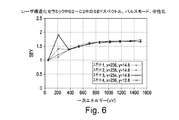
図2は、レーザ処理表面の3つの異なるスポットにおけるサンプルのPSCAの一次電子エネルギーの関数としてのSEYのプロットである。図3は、比較のために、レーザ処理されていないサンプルの裏側の3つの異なるスポットにおける、サンプルのPSCAについての一次電子エネルギーの関数としてのSEYのプロットである。 FIG. 2 is a plot of SEY as a function of PSCA primary electron energy of samples at three different spots of the laser treated surface. FIG. 3 is a plot of SEY as a function of primary electron energy for PSCA of the sample at three different spots on the back side of the unlased sample, for comparison.
PSCAのサンプルの表面のレーザ処理は、SEYの約8から9(未処理裏面の場合)からレーザ処理表面の約2.2への減少をもたらしたことが分かる。 It can be seen that laser treatment of the surface of the PSCA sample resulted in a reduction of about 8 to 9 (for the untreated backside) of SEY to about 2.2 of the laser treated surface.
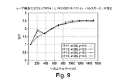
図4から図9は、サンプルのPS1C1R、PS2C1R、PS2C2R、PS2L1R、PS2L2R及びPS4L1Rそれぞれの一次電子エネルギーの関数としてのSEYのプロットである。 FIGS. 4-9 are plots of SEY as a function of primary electron energy for each of the samples PS1C1R, PS2C1R, PS2C2R, PS2L1R, PS2L2R, and PS4L1R.
表1の様々なサンプルの近似した最大SEY値を以下の表2にまとめる。 The approximated maximum SEY values of the various samples of Table 1 are summarized in Table 2 below.
表1のサンプルの走査型電子顕微鏡(SEM)画像を得て、サンプルの表面のレーザ処理によって形成された構造を示す。 A scanning electron microscope (SEM) image of the samples of Table 1 is obtained and shows the structure formed by laser treatment of the surface of the sample.
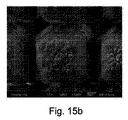
図10aは、サンプルのPSCAのレーザ処理表面のSEM画像である。 FIG. 10a is an SEM image of a laser treated surface of a sample PSCA.
図10bは、PS2L1Rのサンプル(左上の画像)、PS2L2Rのサンプル(左下の画像)、PS2C1Rのサンプル(右上の画像)及びPS2C2Rのサンプル(右下の画像)のレーザ処理表面のSEM画像を示している。 FIG. 10b shows SEM images of the laser treated surface of the PS2L1R sample (upper left image), the PS2L2R sample (lower left image), the PS2C1R sample (upper right image) and the PS2C2R sample (lower right image) There is.
図10cは、PS4L1Rのサンプル(左側画像)及びPS1C1Rのサンプル(右側画像)のレーザ処理表面のSEM画像を示している。 FIG. 10 c shows an SEM image of the laser treated surface of the PS4L1R sample (left image) and the PS1C1R sample (right image).
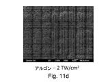
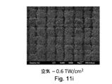
図11aから図11eは、レーザビームの出力密度がそれぞれ0.74TW/cm2、0.88TW/cm2、0.95TW/cm2、2TW/cm2、1.3TW/cm2についてのレーザ処理表面のSEM画像であり、サンプルをアルゴン雰囲気中でレーザ処理されている。図11fから図11jは、レーザビームの出力密度がそれぞれ0.3TW/cm2、0.4TW/cm2、2TW/cm2、0.6TW/cm2及び1TW/cm2についてのレーザ処理表面のSEM画像であり、サンプルは空気中でレーザ処理されている。他の動作パラメータは、表1のサンプルのPSCAと実質的に同じであった。
Figure 11e from Figure 11a, the output density of each 0.74TW / cm 2 of laser beams, 0.88TW / cm 2, 0.95TW / cm 2, 2TW /
(アルゴン雰囲気下で処理された)サンプルのPSCAの通常の拡大されていない図ではサンプルの表面は黒く見えるが、表1の他のサンプルの通常の拡大されていない図ではサンプルの表面は白色に見えるか、又はサンプルのPSCAの表面より少なくともかなり淡く見える。 The surface of the sample appears black in the normal unexpanded view of the sample PSCA (treated in an argon atmosphere), but the surface of the sample is white in the normal unexpanded view of the other samples in Table 1 It looks or appears at least considerably lighter than the surface of the sample PSCA.
酸化アルミニウムのサンプルの分光特性の測定も行った。図12は、レーザ加工の前に、CERNによってキッカー磁石に使用された(C Ceraと呼ばれる、約99.7%の純度を有する)酸化アルミニウムのサンプル及び(ホワイトCeraと呼ばれる)別のサンプルの酸化アルミニウムの全反射率、全透過率及び吸収率を示すグラフである。このスペクトルは、532nmにおけるいくらかの吸収率及び1064nmにおける非常に低い吸収率を示している。反射率は、人間の目に見えるサンプルの異なる色に従うサンプルについて異なる。両方のサンプルの厚さは3mmであった。これらの測定値から、532nm、又は利用可能な他のレーザ波長である515nmでのレーザ処理が適切であることが判明した。 The spectral properties of the aluminum oxide sample were also measured. FIG. 12 shows oxidation of a sample of aluminum oxide (with a purity of about 99.7%, referred to as C Cera) and another sample (referred to as white Cera) used for the kicker magnet by CERN prior to laser processing It is a graph which shows the total reflectance, the total transmittance, and the absorption factor of aluminum. This spectrum shows some absorption at 532 nm and very low absorption at 1064 nm. The reflectivity is different for samples that follow different colors of the human visible sample. The thickness of both samples was 3 mm. From these measurements, laser treatment at 532 nm, or 515 nm, which is another available laser wavelength, proved appropriate.
表1のサンプルのレーザ処理された表面について測定された最大SEY値は、1.6から2.2の間で変化することが、上に概説した結果から分かる。SEYが最も低いサンプルはPS2C1Rであり、最大値は1.6である。サンプルの反射率とSEYとの間には実質的なリンクはないようである。いくつかのサンプルは200eVの電子エネルギーで異常値を有し、これは表面の不均一性に起因するかもしれない。 It can be seen from the results outlined above that the maximum SEY values measured for the lasered surfaces of the samples of Table 1 vary between 1.6 and 2.2. The sample with the lowest SEY is PS2C1R, and the maximum value is 1.6. There appears to be no substantial link between the reflectance of the sample and the SEY. Some samples have outliers at an electron energy of 200 eV, which may be due to surface inhomogeneities.
サンプルがアルミナであるいくつかの他の実施形態では、サンプルの表面に所望の構造の周期的な配置を作成するように、以下のように動作パラメータを表3から選択してもよい。動作パラメータの値は、他の興味のあるセラミック材料の場合にも表3から選択してもよい。 In some other embodiments where the sample is alumina, the operating parameters may be selected from Table 3 as follows to create a periodic arrangement of the desired structure on the surface of the sample. The operating parameter values may also be selected from Table 3 for other ceramic materials of interest.
アルゴン中のレーザ処理について、0.1TW/cm2から3TW/cm2の出力密度の範囲で良好な結果が得られ、532nmの波長について0.5TW/cm2から1.5TW/cm2の出力密度の範囲で特に良好な結果が得られてもよい。しかしながら、高度に組織化された構造化は、空気又はアルゴンのいずれかでのレーザ加工に対して達成される。 The laser treatment in argon, 0.1TW / cm good results from 2 in a range of power density of 3 Tw / cm 2 is obtained, the output for the wavelength of 532nm from 0.5 TW / cm 2 of 1.5TW / cm 2 Particularly good results may be obtained in the density range. However, highly organized structuring is achieved for laser processing with either air or argon.
表1から表3及び図2から図12に関連して上述した結果は、TW/cm2の範囲のレーザビーム出力密度を用いて得られた。別の実施形態では、セラミック表面のレーザパターニングは、GW/cm2の範囲のレーザビーム出力密度を使用して得られる。 The results described above in connection with Tables 1 to 3 and FIGS. 2 to 12 were obtained using laser beam power densities in the range of TW / cm 2 . In another embodiment, laser patterning of the ceramic surface is obtained using laser beam power density in the range of GW / cm 2 .
表4は、図1の装置のレーザの動作パラメータを提供し、GW/cm2のレーザビーム出力密度を使用して、アルミナのサンプル(NSCAのサンプルと呼ぶ)の表面に所望の構造の周期的な配置を作成する。表面のレーザ処理は、NSCAのサンプルについてアルゴン雰囲気中で行った。 Table 4 provides the operating parameters of the laser of the apparatus of FIG. 1 and uses the laser beam power density of GW / cm 2 to periodically form the desired structure on the surface of an alumina sample (referred to as an NSCA sample) Create an arrangement. Laser treatment of the surface was performed on the NSCA sample in an argon atmosphere.
表4は、TW/cm2の範囲のレーザ出力密度で処理された特定のサンプルの動作パラメータを提供した表1と同じフォーマットである。 Table 4 is the same format as Table 1 which provided the operating parameters of a particular sample processed at a laser power density in the range of TW / cm 2 .
表1のNSCAのサンプルは3mmの厚さを有し、サンプルのレーザ加工領域は14mm×14mmであった。サンプルは、99.7%以上の純度を有する酸化アルミニウム(アルミナ)であり、これは特定の粒子加速器用途に用いられる等級である。 The NSCA sample of Table 1 had a thickness of 3 mm, and the laser processed area of the sample was 14 mm × 14 mm. The sample is aluminum oxide (alumina) with a purity of 99.7% or higher, which is the grade used for certain particle accelerator applications.
表4のNSCAのサンプルの二次電子収量(SEY)を、サンプルの3つの異なるスポットにおける異なる一次電子エネルギーについて測定した。帯電効果を避けるために、各測定点の間で低エネルギー電子(36eV)を表面に衝突させた。一つのデータ点を測定するための最大照射線量は約1×10⁻¹²Cであった。したがって、一つのスペクトルを測定するための総線量は約1×10⁻¹¹Cであった。 The secondary electron yield (SEY) of the NSCA samples of Table 4 was measured for different primary electron energies at three different spots of the sample. Low energy electrons (36 eV) were collided with the surface between each measurement point to avoid the charging effect. The maximum irradiation dose for measuring one data point was about 1 × 10 −12 C. Thus, the total dose to measure one spectrum was about 1 × 10 −11 C.
図13は、サンプルのNSCAについてレーザ処理された表面の3つの異なるスポットにおける一次電子エネルギーの関数としてのSEYのプロットである。 FIG. 13 is a plot of SEY as a function of primary electron energy at three different spots of the lasered surface of the sample for NSCA.
SEY測定の実施後、500eVの電子で1×10⁻²C/mm2の総線量までサンプルに衝突させることによって、より低いSEY値が得られるようにNSCAのサンプルをコンディショニングし、次に一晩にわたりサンプルを空気に暴露した。 After performing the SEY measurement, condition the NSCA sample to obtain a lower SEY value by colliding the sample with a total dose of 1 x 10 -2 C / mm 2 with 500 eV electrons, and then overnight The samples were exposed to air over time.
図14は、サンプルのNSCAについて500eVの電子を用いて空気に暴露した後でレーザ処理された表面の3つの異なるスポットにおける一次電子エネルギーの関数としてのSEYのプロットである。比較のために図13のSEY結果も図14に含まれている。 FIG. 14 is a plot of SEY as a function of primary electron energy at three different spots on a laser treated surface after exposure to air with 500 eV electrons for sample NSCA. The SEY results of FIG. 13 are also included in FIG. 14 for comparison.
コンディショニング及び空気曝露後に得られた図14のSEY結果は、最大SEYが増加を示すことが判明し、反応性の表面を示唆している。コンディショニング及び空気暴露後のSEYスペクトルの測定値は再現性が良くなかったが、その理由はセラミックのバルクに電荷を注入することであるかも知れない。 The SEY results of FIG. 14 obtained after conditioning and air exposure were found to show an increase in maximum SEY, suggesting a reactive surface. The SEY spectra measurements after conditioning and air exposure were not repeatable, which may be due to the injection of charge into the bulk of the ceramic.
NSCAのサンプルの表面の帯電を確認するために、コンディショニング及び空気曝露後にXPSスペクトルを得るためのX線光電子分光測定を行った。XPSスペクトルは、アルミニウム(15原子%)と酸素(79原子%)が主な元素であり、炭素汚染が低く(1原子%)、フッ素が一部(5原子%)存在することを示した。 X-ray photoelectron spectroscopy measurements to obtain XPS spectra after conditioning and air exposure were performed to confirm the surface charge of the NSCA sample. The XPS spectrum showed that aluminum (15 at%) and oxygen (79 at%) were the main elements, carbon contamination was low (1 at%) and fluorine was partially (5 at%).
図15a及び図15bは、サンプルのNSCAのレーザ処理された表面の異なる倍率レベルでのSEM画像である。 Figures 15a and 15b are SEM images at different magnification levels of the NSCA laser-treated surface of the sample.
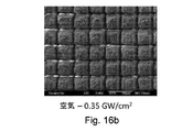
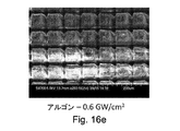
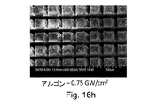
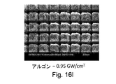
図16aから図16dは、レーザビームの出力密度がそれぞれ0.25GW/cm2、0.35GW/cm2、0.45GW/cm2、及び0.55GW/cm2であるレーザ処理表面のSEM画像であり、サンプルは空気中でレーザ処理された。図16eから図16nは、レーザビームの出力密度がそれぞれ0.6GW/cm2、0.65GW/cm2、0.7GW/cm2、0.75GW/cm2、0.8GW/cm2、0.85GW/cm2、0.9GW/cm2、0.95GW/cm2、1GW/cm2、及び1.5GW/cm2であり、サンプルをアルゴン雰囲気中でレーザ処理した。他の動作パラメータは、表4のサンプルのNSCAと実質的に同じであった。
Figure 16d from Figure 16a, 0.25GW / cm 2 power density of the laser beam, respectively, 0.35GW /
サンプルがアルミナであるいくつかの他の実施形態では、以下のように動作パラメータを表5から選択して、サンプルの表面に所望の構造の周期的な配置を作成してもよい。動作パラメータの値は、他の興味のあるセラミック材料の場合には表5から選択してもよい。 In some other embodiments where the sample is alumina, the operating parameters may be selected from Table 5 as follows to create a periodic arrangement of the desired structure on the surface of the sample. The values of the operating parameters may be selected from Table 5 for other ceramic materials of interest.
出力密度の範囲が0.1GW/cm2から3GW/cm2で良好な結果が達成され、出力密度の範囲が0.2GW/cm2から1GW/cm2で532nmの波長に対して特に良好な結果が得られた。しかし、高度に組織化された構造化は、空気又はアルゴンのいずれかでのレーザ加工に対して達成される。 Range of power density is achieved good results in 3GW / cm 2 from 0.1GW / cm 2, the range of the output density is particularly good for the wavelength of 532nm from 0.2 GW / cm 2 at 1 GW / cm 2 The results were obtained. However, highly organized structuring is achieved for laser processing with either air or argon.
実施形態の特徴は、TW/cm2又はGW/cm2の範囲の出力密度を有するレーザ放射を表面に照射することによって、セラミック表面に周期構造を形成することができることである。理論に縛られることを望むことはなく、保護の範囲を限定することなく、少なくともいくつかの実施形態に関連して起こり得るプロセスに関する以下のコメントが提供される。 A feature of the embodiments is that periodic structures can be formed on the ceramic surface by irradiating the surface with laser radiation having a power density in the range of TW / cm 2 or GW / cm 2 . Without wishing to be bound by theory, and without limiting the scope of protection, the following comments regarding processes that may occur in connection with at least some embodiments are provided.
レーザ工学は、実施形態による周期構造の形成を提供する最も包括的な方法論を提供する。精密レーザ工学は、金属内の自由電子、絶縁体内の振動、そして実際に半導体内の両方のタイプの励起を励起することが期待されている。レーザが材料を設計するメカニズムは次の事項を含んでいる。 Laser engineering provides the most comprehensive methodology that provides for the formation of periodic structures according to embodiments. Precision laser engineering is expected to excite free electrons in metals, vibrations in insulators, and indeed both types of excitation in semiconductors. The mechanism by which the laser designs the material includes the following.
(i)光熱相互作用(PTI) 短い滞留時間を提供するレーザビーム(例えば、ナノ秒のパルス幅を有するレーザ)を使用して一般的に達成される。
(ii)光アブレーション相互作用(PAI) 超短滞留時間を提供するレーザビーム(例えば、ピコ秒又はフェムト秒パルス幅を有するレーザ)を使用して想定される。
(I) Photothermal Interaction (PTI) This is generally accomplished using a laser beam (eg, a laser with a nanosecond pulse width) that provides a short residence time.
(Ii) Photoablation Interaction (PAI) A laser beam (eg, a laser with picosecond or femtosecond pulse width) providing ultrashort residence time is envisioned.
表4及び5及び図13から図16に関連して説明した実施形態に関するレーザ処理は、PTI領域ですることができる。表1から表3及び図2から図11に関連して説明した実施形態に関するレーザ処理は、PAI領域ですることができる。 Laser processing for the embodiments described in connection with Tables 4 and 5 and FIGS. 13-16 may be in the PTI region. The laser processing for the embodiments described in connection with Tables 1 to 3 and FIGS. 2 to 11 can be done in the PAI region.
PTI領域では、集束されたレーザビームは、空間的に閉じ込められた強い熱源として働く。ターゲット物質は急速に加熱され、最終的には気化する。保護範囲の制限を示唆することを望まないが、ターゲット物質は沸騰して蒸発したと呼ぶことができる。このアプローチの利点は、比較的多量のターゲット材料の迅速な除去を可能にすることである。しかしながら、周辺の熱影響部(HAZ)の損傷及び処理後のいくらかのリキャスト材料の存在は、精密レーザ材料工学のための熱閉じ込めの点で限界をもたらす。 In the PTI region, the focused laser beam acts as a spatially confined strong heat source. The target material is rapidly heated and eventually vaporized. While not wishing to suggest a limitation of the protective range, the target material can be said to boil and evaporate. An advantage of this approach is that it allows for the rapid removal of relatively large amounts of target material. However, damage to the peripheral heat affected zone (HAZ) and the presence of some recast material after processing present limitations in terms of thermal confinement for precision laser material engineering.
PAI領域では、レーザは材料内の光で多光子吸収を駆動する。これは、材料から電子を取り除き、材料はクーロン反発のために爆発する。PAIは、単純に加熱するのではなく、物質を保持する分子結合又は原子結合を直接破壊することを含むため、本質的に「熱い」プロセスではない。材料は非常に短い時間枠内で除去されるので、アブレーションされた材料は周囲の材料に熱が広がる前に大部分のエネルギーを持ち去る。これらの影響により、HAZが著しく縮小することがある。また、これはきれいなプロセスであり、リキャスト材料を最小限に抑えることができるため、手の込んだ後処理の必要性が排除される。PAI領域は、線形の光吸収が低く、したがって既存の技術では設計が困難な高バンドギャップ材料を含む、非常に広範囲の材料に適合する。PAIメカニズムは「波長中性」、すなわち、材料がレーザ波長で通常は透過性であっても、非線形吸収を低減することができると考えられる。 In the PAI region, the laser drives multiphoton absorption with light in the material. This removes the electrons from the material and the material explodes due to Coulomb repulsion. PAI is not an essentially "hot" process as it involves the direct destruction of molecular or atomic bonds that hold the material rather than simply heating. Since the material is removed in a very short time frame, the ablated material carries away most of the energy before the heat spreads to the surrounding material. These effects can cause the HAZ to shrink significantly. Also, this is a clean process and can minimize recast material, eliminating the need for elaborate post-processing. The PAI region is compatible with a very wide range of materials, including high band gap materials, which have low linear light absorption and are therefore difficult to design with existing technologies. It is believed that the PAI mechanism can reduce non-linear absorption, "wavelength neutral", ie, even though the material is normally transparent at the laser wavelength.
PAIメカニズムは、セラミック表面の電子仕事関数のカスタム設計を根本的に可能にするであろう。セラミックは、通常、金属イオンと非金属原子とで構成され、硬度、脆さ、耐熱性などの特性を与える、部分的にイオン性で部分的に共有結合による結合で結合されている。したがって、これらの材料における光物質相互作用メカニズムにおいて重要な役割を果たすことがあり、最終的にはレーザ精密構造化プロセスの問題とセラミック表面の表面電位の設計に寄与することがあるパラメータを正確に特定することは重要性であることがある。 The PAI mechanism will fundamentally allow custom design of the electronic work function of the ceramic surface. Ceramics are usually composed of metal ions and nonmetal atoms and are partially ionically and partially covalently bonded to give properties such as hardness, brittleness, heat resistance and the like. Therefore, it may play an important role in the light-matter interaction mechanism in these materials, and ultimately, the parameters of the laser microstructuring process and the parameters that may contribute to the design of the surface potential of the ceramic surface Identifying can be important.
PTI及びPAIメカニズムは、それぞれ図17a及び図17bに概略的に示されている。 The PTI and PAI mechanisms are shown schematically in FIGS. 17a and 17b respectively.
実施形態のさらなる特徴は、例えばピコ秒範囲以下のパルス持続時間を使用した、表面に照射されるパルス放射の特性が、形成される周期構造がより高いエネルギーのパルス放射及び/又は例えばナノ秒範囲の持続時間のパルスのようなより長い持続時間を用いて形成されたものより、より浅い深さであってもよく、及び/又はより緩やかに傾斜してもよいようなものであるということである。 A further feature of the embodiment is that the characteristic of the pulsed radiation with which the surface is irradiated, for example using a pulse duration below the picosecond range, is pulsed radiation with higher energy in the periodic structure formed and / or for example the nanosecond range So that it may be shallower and / or may be sloped more gently than those formed with longer durations, such as pulses of duration is there.
やはり、理論に縛られることを望むことはなく、保護の範囲を限定するものではないが、少なくともいくつかの実施形態に関連して起こることがあるプロセスに関する以下のさらなるコメントが提供される。 Again, without wishing to be bound by theory, and not limiting the scope of protection, the following additional comments on processes that may occur in connection with at least some embodiments are provided.
非常に高い強度(又は高照度)での照射では、濃い、強く吸収する物質の問題に直面し、最初の数十nmにおいて約1020W/cm3の速度でエネルギーが解放される。このエネルギーの一部は、一度無作為化され、材料のバルクに伝導され、一部は加熱された層の熱膨張によって指向性運動エネルギーに変換される。二つの領域は、この点で区別される。 Irradiation at very high intensity (or high intensity) encounters the problem of dark, strongly absorbing materials and releases energy at a rate of about 10 20 W / cm 3 in the first few tens of nm. A portion of this energy is randomized once and conducted to the bulk of the material and a portion is converted to directed kinetic energy by thermal expansion of the heated layer. The two regions are distinguished in this respect.
1.ナノ秒パルス状レーザ相互作用であり、材料の膨張及びアブレーションによって支配される。ここでは、加熱された層の熱圧力は、下にあるターゲット材料の著しい圧縮を引き起こすのに十分である。 1. Nanosecond pulsed laser interaction, dominated by expansion and ablation of the material. Here, the thermal pressure of the heated layer is sufficient to cause significant compression of the underlying target material.
2.ピコ秒パルス状レーザ相互作用(熱伝導が支配的であるが、これはパルス持続時間の間の流体力学的運動は無視できるためである(ここでのレーザパルスはナノ秒よりも1000倍以上短くてよい)。ピコ秒領域では、処理された層の流体力学的膨張が開始される前に、高密度材料の強い加熱が起こってもよい。この領域で生成されたプラズマは、固体ターゲットそれ自体と本質的に同じ密度を有してもよい。これによって、冷却すると、照射パラメータに応じて、ナノ構造で覆われた1マイクロメートルから50マイクロメートルの範囲の微細構造が形成される。 2. Picosecond pulsed laser interaction (heat conduction dominates, because the hydrodynamic motion during the pulse duration is negligible (the laser pulse here is more than 1000 times shorter than nanoseconds) In the picosecond region, strong heating of the high density material may occur before hydrodynamic expansion of the treated layer is initiated The plasma generated in this region is the solid target itself It may have essentially the same density as that, upon cooling, depending on the irradiation parameters, it will form microstructures in the range of 1 micrometer to 50 micrometers covered with nanostructures.
いくつかの実施形態によれば、ピコ秒持続時間パルス放射を用いると、場合によっては、表面を適切なパターンのレーザビームで走査することによって得られるより大きなスケールのピーク及びトラフに加えて、表面にナノリップル又は他の小規模構造の形成を引き起こすことができる。このようなナノリップル又は他の小規模構造は、より大きな周期的なピーク及びトラフ構造によって得られる減少に加えて、場合によってはPEY又はSEYをさらに減少させてもよい。また、いくつかの場合には、ナノ秒パルスではなくピコ秒に関連するナノリップル又は他の小規模構造及び/又は浅いピーク及びトラフが、例えば、表面の改善された又は誘導の低減のような代替の電気的特性を提供してもよく、及び/又は表面にナノ又はマイクロスケールで増加した領域を提供することができる。 According to some embodiments, with picosecond duration pulsed radiation, in some cases, in addition to the larger scale peaks and troughs obtained by scanning the surface with a laser beam of appropriate pattern, the surface Can cause the formation of nano ripples or other small scale structures. Such nanoripples or other small scale structures may optionally further reduce PEY or SEY, in addition to the reduction obtained by the larger periodic peak and trough structures. Also, in some cases, nanoripples or other small scale structures and / or shallow peaks and troughs associated with picoseconds rather than nanosecond pulses, such as, for example, improved or reduced surface induction Alternative electrical properties may be provided and / or the surface may be provided with increased area on the nano or micro scale.
やはり、理論に縛られることを望むことはなく、保護の範囲を限定することなく、さらなるコメントは以下の通りである。 Again, without wishing to be bound by theory, without limiting the scope of protection, further comments are as follows.
表面粗さが増すにつれて、最大SEYはより多くの谷を特徴とする(例えば、統計的に含む)表面について減少することがあり、より多くの丘が広がる(例えば、統計的に含む)表面で有意に増加することがある。この観察は、異なる形態学的特徴及び表面電子仕事関数(EWF)に起因して、丘及び谷構造がSEYのそれぞれ増加及び減少に増減に非常に有効であることを示している。 As surface roughness increases, maximum SEY may decrease for surfaces characterized by more valleys (eg, statistically included) and more hills spread (eg, statistically included) at the surface May increase significantly. This observation indicates that hill and valley structures are very effective at increasing and decreasing SEY respectively due to different morphological features and surface electronic work functions (EWF).
総SEYは、表面に入射した一次電子(PE)に対する放出された真の二次電子(SE)及び反射電子(BSE)の両方の比率を示してもよい。 The total SEY may indicate the ratio of both the emitted true secondary electrons (SE) and the reflected electrons (BSE) to the primary electrons (PE) incident on the surface.
例:空気にさらされたサンプルの表面は、吸着したガスや炭化水素によって容易に汚染され、SEYが増加することがある。 Example: The surface of a sample exposed to air can be easily contaminated by adsorbed gases and hydrocarbons, and SEY can increase.
汚染によって引き起こされた高いSEYは、電子増倍を生じさせ、最終的にはマイクロ波デバイスの性能を低下させ、大規模粒子加速器における破壊的電子クラウド不安定性を低下させるであろう。 The high SEY caused by the contamination will cause electron multiplication and ultimately reduce the performance of the microwave device and reduce destructive electron cloud instability in large scale particle accelerators.
SEYの増加は、電子仕事関数(EWF)の減少を示す。 An increase in SEY indicates a decrease in the electronic work function (EWF).
粗さが増すにつれて、SEYmaxは丘によって隔てられた表面について顕著な増加を有する。この現象は、丘構造がSE放出において積極的な役割を果たすであろうことを示唆している。また、SEYmaxは、主に谷で特徴付けられる表面によって急速に減少し、これはSEYmaxが減少する支配的な要因であろう。 As the roughness increases, SEYmax has a significant increase for surfaces separated by hills. This phenomenon suggests that the hill structure will play an active role in SE release. Also, SEYmax decreases rapidly with the surface characterized mainly by valleys, which may be the dominant factor that decreases SEYmax.
谷構造の場合、SEは側壁との衝突によって効果的に捕獲することができ、したがってSEYは減少する。それにもかかわらず、丘構造については、側壁の負の効果とは別に、SE放出にいくつかの正の効果がある。例えば、いくつかのPEは、丘を有する局所的な表面に斜めに当たり、通常の入射より多くのSEを誘導する。さらに、SEは丘の側壁に再突入することがあり、その結果としてさらにSEが発生する。ほとんどの再入射するSEは、表面ポテンシャル障壁を克服し、真空に逃げる低エネルギーで多くの真のSEを生成する高エネルギーのBSEであろう。 In the case of a valley structure, SE can be effectively captured by collisions with the sidewalls, thus SEY is reduced. Nevertheless, for hill structures, apart from the negative effects of the sidewalls, there are some positive effects on SE emission. For example, some PEs strike diagonally on a localized surface with hills, inducing more SE than normal incidence. Furthermore, the SE may re-enter the side wall of the hill, which results in further SE. Most re-incident SEs will be high-energy BSEs that overcome surface potential barriers and generate many true SEs at low energy to escape vacuum.
異なる表面形態によって誘導される電子仕事関数(EWF)の変化も、SEY変動の原因となることがある。仕事関数は、表面のピークで減少し、表面の粗さが増加するにつれて表面の谷で増加する。構造化作業における丘と谷は、表面のピークと谷とみなすことができる。丘構造によって導入されたより粗い表面は、しばしば電子仕事関数(EWF)がより低く、したがってSEYは自然に増加する。しかし、EWFは谷構造で表面を粗くすることによって強化され、最終的にSEYが減少する。 Changes in the electronic work function (EWF) induced by different surface morphologies may also contribute to SEY fluctuations. The work function decreases at surface peaks and increases at surface valleys as the surface roughness increases. The hills and valleys in the structuring operation can be regarded as surface peaks and valleys. The rougher surfaces introduced by the hill structure often have lower electronic work functions (EWFs) and thus SEY increases naturally. However, EWF is enhanced by roughening the surface in the valley structure, which ultimately reduces SEY.
周期構造を形成するレーザ処理後のセラミック表面上に金属層を形成することにより、SEYの有意な減少がもたらされることが分かった。図18は、厚さ10nmの金層で被覆する前と後の両方で、上述のサンプル名PS2C1R及びPS2C1Rを有するアルミナセラミックのサンプルの一次エネルギーの関数として測定されたSEYのプロットである。両方のサンプルについてSEYの有意な減少が見られることが分かる。 It has been found that forming the metal layer on the ceramic surface after laser treatment to form the periodic structure results in a significant reduction of SEY. FIG. 18 is a plot of SEY measured as a function of primary energy of a sample of alumina ceramic having sample names PS2C1R and PS2C1R, both before and after coating with a 10 nm thick gold layer. It can be seen that a significant decrease in SEY is seen for both samples.
図19及び20は、金層でコーティングした後のPS2C1R及びPS2C1Rアルミナサンプルの表面のSEM画像を示している。 Figures 19 and 20 show SEM images of the surface of PS2C1R and PS2C1R alumina samples after being coated with a gold layer.
別の実施形態では、任意の他の適切な厚さの任意の他の適切な金属をセラミック表面の金属層に使用することができる。 In another embodiment, any other suitable metal of any other suitable thickness can be used for the metal layer of the ceramic surface.
金又は他の金属の層は、任意の適切な堆積プロセス、例えば、スパッタリングプロセス、蒸発堆積プロセス又はレーザ堆積プロセスなどの任意の適切な化学的又は物理的蒸着プロセスを使用して形成することができる。一例として、コーティングを形成するためにエドワーズ(RTM)308コーティングユニットを用いてもよい。任意の他の適切な堆積装置を使用してもよい。 The layer of gold or other metal can be formed using any suitable deposition process, for example any suitable chemical or physical vapor deposition process such as sputtering process, evaporation deposition process or laser deposition process . As an example, an Edwards (RTM) 308 coating unit may be used to form the coating. Any other suitable deposition device may be used.
別の実施形態では、セラミック表面、又はセラミック表面に堆積された金属層には、レーザ放射の照射の後で脱脂、洗浄又は平滑化プロセス及び/又は表面炭素還元プロセスが施されることがあり、それによってSEYが低減することがある。NGL(RTM)脱脂製品を使用した洗浄を使用してもよい。代替実施形態では、任意の適切な脱脂、洗浄、平滑化又は表面炭素還元プロセスを使用してもよい。一部の実施形態では、脱脂剤は、サンプルの形態を実質的に変化させないが、炭素又は炭素含有化合物の層、混合物又は他の材料又は他の望ましくない及び/又は外来の化合物、混合物又は材料、例えば金属酸化物、グリース又は汚れを表面から除去してもよい。例えば、いくつかの実施形態では、表面形態を実質的に変化させることなく、例えば銅(I)及び銅(II)酸化物及び/又は他の物質のような表面物質を除去するために、99.7%の氷酢酸(任意の他の適切な濃度を使用することができる)を使用してもよい。 In another embodiment, the ceramic surface or metal layer deposited on the ceramic surface may be subjected to a degreasing, cleaning or smoothing process and / or a surface carbon reduction process after irradiation with laser radiation. This may reduce SEY. Cleaning using NGL (RTM) defatted products may be used. In alternative embodiments, any suitable degreasing, washing, smoothing or surface carbon reduction process may be used. In some embodiments, the degreasing agent does not substantially change the form of the sample, but a layer or mixture of carbon or carbon containing compounds or other material or other undesirable and / or extraneous compound, mixture or material For example, metal oxides, greases or dirt may be removed from the surface. For example, in some embodiments, to remove surface materials such as, for example, copper (I) and copper (II) oxides and / or other materials, without substantially changing the surface morphology. 7% glacial acetic acid (any other suitable concentration may be used) may be used.
以上、本発明を純粋に例示によって説明してきたが、本発明の範囲内で詳細の変更を行うことができることは理解されよう。説明の各特徴、及び(適切な場合には)図面は、独立して、又は他のそのような特徴と適切に組み合わせて提供されてもよい。
While the invention has been described purely by way of example, it will be understood that modifications of detail can be made within the scope of the invention. Each feature of the description, and (where appropriate) the drawings may be provided independently or in appropriate combination with other such features.
Claims (33)
パルス状のレーザ放射を表面に照射するレーザ源と、
セラミック表面に構造の周期的な配置を作成するように、レーザ放射を一連のレーザパルスとして照射するように前記レーザ源を制御するように構成されたレーザコントローラと
を含む装置。 An apparatus for reducing the photoelectron yield (PEY) and / or the secondary electron yield (SEY) of a ceramic surface, comprising:
A laser source for irradiating the surface with pulsed laser radiation;
A laser controller configured to control the laser source to emit laser radiation as a series of laser pulses to create a periodic arrangement of structures on a ceramic surface.
33. The laser treated ceramic surface of claim 32, further comprising a metal layer covering at least a portion of the periodic arrangement of the structures.
Applications Claiming Priority (3)
| Application Number | Priority Date | Filing Date | Title |
|---|---|---|---|
| GBGB1603991.9A GB201603991D0 (en) | 2016-03-08 | 2016-03-08 | Processing method and apparatus |
| GB1603991.9 | 2016-03-08 | ||
| PCT/GB2017/050621 WO2017153750A1 (en) | 2016-03-08 | 2017-03-08 | Method of reducing photoelectron yield and/or secondary electron yield of a ceramic surface; corresponding apparatus and product |
Publications (2)
| Publication Number | Publication Date |
|---|---|
| JP2019508256A true JP2019508256A (en) | 2019-03-28 |
| JP2019508256A5 JP2019508256A5 (en) | 2020-02-06 |
Family
ID=55859181
Family Applications (1)
| Application Number | Title | Priority Date | Filing Date |
|---|---|---|---|
| JP2018546883A Pending JP2019508256A (en) | 2016-03-08 | 2017-03-08 | Method of reducing photoelectron yield and / or secondary electron yield on ceramic surfaces and corresponding devices and products |
Country Status (11)
| Country | Link |
|---|---|
| US (1) | US10994369B2 (en) |
| EP (1) | EP3397421A1 (en) |
| JP (1) | JP2019508256A (en) |
| KR (1) | KR20190015180A (en) |
| CN (1) | CN109070266B (en) |
| AU (1) | AU2017231862A1 (en) |
| BR (1) | BR112018067765A2 (en) |
| CA (1) | CA3015159A1 (en) |
| GB (1) | GB201603991D0 (en) |
| RU (1) | RU2018135083A (en) |
| WO (1) | WO2017153750A1 (en) |
Families Citing this family (1)
| Publication number | Priority date | Publication date | Assignee | Title |
|---|---|---|---|---|
| CN111215399A (en) * | 2020-02-27 | 2020-06-02 | 长安大学 | Method for reducing secondary electron emission coefficient by inert ion cleaning and heat treatment |
Citations (10)
| Publication number | Priority date | Publication date | Assignee | Title |
|---|---|---|---|---|
| JPS4834667A (en) * | 1971-09-08 | 1973-05-21 | ||
| JPH05325780A (en) * | 1992-05-14 | 1993-12-10 | Nec Corp | Manufacture of collector electrode for microwave tube |
| JP2000311632A (en) * | 1998-10-07 | 2000-11-07 | Canon Inc | Electron beam device and spacer |
| JP2003303561A (en) * | 2002-04-10 | 2003-10-24 | Canon Inc | Spacer, method of manufacturing spacer, and electron beam device |
| JP2010050138A (en) * | 2008-08-19 | 2010-03-04 | Canon Machinery Inc | Method of forming minute cyclic structure |
| JP2013111595A (en) * | 2011-11-28 | 2013-06-10 | Shin Etsu Polymer Co Ltd | Method of processing metal mold and method of forming emblem |
| JP2013529548A (en) * | 2010-06-25 | 2013-07-22 | エレクトロ サイエンティフィック インダストリーズ インコーポレーテッド | Method and apparatus for reliably laser marking an object |
| US20140175067A1 (en) * | 2012-12-20 | 2014-06-26 | Electro Scientific Industries, Inc. | Methods of forming images by laser micromachining |
| JP2014133263A (en) * | 2007-01-23 | 2014-07-24 | Imra America Inc | Ultrashort laser micro-texture printing |
| JP2018524182A (en) * | 2015-06-24 | 2018-08-30 | ユニバーシティー オブ ダンディーUniversity Of Dundee | Method and apparatus for reducing photoelectron yield and / or secondary electron yield |
Family Cites Families (41)
| Publication number | Priority date | Publication date | Assignee | Title |
|---|---|---|---|---|
| JPH0640797A (en) | 1992-04-23 | 1994-02-15 | Sumitomo Electric Ind Ltd | Method for machining diamond |
| US6518540B1 (en) * | 1998-06-16 | 2003-02-11 | Data Storage Institute | Method and apparatus for providing ablation-free laser marking on hard disk media |
| US7838794B2 (en) * | 1999-12-28 | 2010-11-23 | Gsi Group Corporation | Laser-based method and system for removing one or more target link structures |
| US6407363B2 (en) | 2000-03-30 | 2002-06-18 | Electro Scientific Industries, Inc. | Laser system and method for single press micromachining of multilayer workpieces |
| JP4578710B2 (en) * | 2001-03-28 | 2010-11-10 | 独立行政法人科学技術振興機構 | Method of creating domain-inverted structure by femtosecond laser irradiation |
| GB0112234D0 (en) | 2001-05-18 | 2001-07-11 | Welding Inst | Surface modification |
| US9409254B2 (en) | 2005-09-30 | 2016-08-09 | Lawrence Livermore National Security, Llc | Ablation layers to prevent pitting in laser peening |
| US8846551B2 (en) * | 2005-12-21 | 2014-09-30 | University Of Virginia Patent Foundation | Systems and methods of laser texturing of material surfaces and their applications |
| US7628865B2 (en) | 2006-04-28 | 2009-12-08 | Asml Netherlands B.V. | Methods to clean a surface, a device manufacturing method, a cleaning assembly, cleaning apparatus, and lithographic apparatus |
| US20080299408A1 (en) | 2006-09-29 | 2008-12-04 | University Of Rochester | Femtosecond Laser Pulse Surface Structuring Methods and Materials Resulting Therefrom |
| US20080216926A1 (en) | 2006-09-29 | 2008-09-11 | Chunlei Guo | Ultra-short duration laser methods for the nanostructuring of materials |
| DE102007018402A1 (en) * | 2007-04-17 | 2008-10-23 | Panasonic Electric Works Europe Ag | Method for introducing a structure into a surface of a transparent workpiece |
| CA2690559A1 (en) * | 2007-06-12 | 2008-12-24 | Technolines, Llc | High speed and high power laser scribing methods and systems |
| CN102186672B (en) | 2008-10-22 | 2015-08-26 | 东洋制罐株式会社 | There is the laminate structures of fine periodic structure |
| US9993895B2 (en) | 2009-03-30 | 2018-06-12 | Boegli-Gravures Sa | Method and device for structuring the surface of a hard material coated solid body by means of a laser |
| US20110089039A1 (en) | 2009-10-16 | 2011-04-21 | Michael Nashner | Sub-Surface Marking of Product Housings |
| EP2336810A1 (en) | 2009-12-18 | 2011-06-22 | Boegli-Gravures S.A. | Method and device for generating colour patterns using a diffraction grating |
| US8379678B2 (en) | 2010-02-11 | 2013-02-19 | Electro Scientific Industries, Inc. | Method and apparatus for reliably laser marking articles |
| US8451873B2 (en) | 2010-02-11 | 2013-05-28 | Electro Scientific Industries, Inc. | Method and apparatus for reliably laser marking articles |
| US8743165B2 (en) | 2010-03-05 | 2014-06-03 | Micronic Laser Systems Ab | Methods and device for laser processing |
| WO2011123515A1 (en) | 2010-03-30 | 2011-10-06 | Sun Chemical Corporation | A reversible piezochromic system, methods of making a reversible piezochromic system, and methods of using a reversible piezochromic system |
| KR20130031377A (en) * | 2010-07-12 | 2013-03-28 | 필레이저 유에스에이 엘엘시 | Method of material processing by laser filamentation |
| GB201011720D0 (en) | 2010-07-13 | 2010-08-25 | Univ Southampton | Controlling the colours of metals: bas-relief and intaglio metamaterials |
| RU2447012C1 (en) | 2010-10-28 | 2012-04-10 | Российская Федерация, от имени которой выступает Министерство промышленности и торговли Российской Федерации (Минпромторг России) | Method of producing steel nanostructured surface by laser-induced plasma processing |
| US20130083500A1 (en) | 2011-09-30 | 2013-04-04 | Christopher D. Prest | Interferometric color marking |
| CH708023B1 (en) | 2012-03-12 | 2018-06-29 | Rolex Sa | A method of engraving a timepiece and a timepiece obtained by such a method. |
| CN103304276B (en) * | 2012-03-14 | 2015-11-25 | 比亚迪股份有限公司 | A kind of metallized method of ceramic base plate surface and a kind of great power LED base |
| PL222531B1 (en) | 2012-04-05 | 2016-08-31 | Wrocławskie Centrum Badań Eit + Spółka Z Ograniczoną | Method and system for color marking of metals |
| US20140083984A1 (en) | 2012-09-23 | 2014-03-27 | Timothy Gerke | Formation Of Laser Induced Periodic Surface Structures (LIPSS) With Picosecond Pulses |
| FR2996487B1 (en) * | 2012-10-08 | 2014-11-28 | Snecma | SURFACE MARKING METHOD OF A GAS TURBINE ENGINE PART BY A PREFINED GRAPHICAL REPRESENTATION |
| GB201221184D0 (en) | 2012-11-24 | 2013-01-09 | Spi Lasers Uk Ltd | Method for laser marking a metal surface with a desired colour |
| US9413137B2 (en) | 2013-03-15 | 2016-08-09 | Nlight, Inc. | Pulsed line beam device processing systems using laser diodes |
| JP6079505B2 (en) * | 2013-08-26 | 2017-02-15 | 三菱マテリアル株式会社 | Bonded body and power module substrate |
| CN103586578B (en) | 2013-11-14 | 2016-08-31 | 苏州图森激光有限公司 | A kind of material surface laser melanism or color method |
| FR3019074B1 (en) * | 2014-04-01 | 2016-04-15 | Snecma | METHOD FOR SURFACE MARKING A MECHANICAL PIECE BY PREDEFINED GRAPHICAL REPRESENTATION WITH HOLOGRAPHIC TYPE EFFECT |
| GB2527291B (en) | 2014-06-13 | 2021-01-13 | Res & Innovation Uk | Apparatus and methods relating to reduced photoelectron yield and/or secondary electron yield |
| ES2564054B1 (en) * | 2014-09-16 | 2016-12-27 | Consejo Superior De Investigaciones Científicas (Csic) | Anti-multipactor coating |
| EP3031785B1 (en) * | 2014-12-12 | 2018-10-17 | Schott AG | Method for producing a glass ceramic element having a structured coating |
| CN104741852B (en) * | 2015-03-19 | 2016-05-25 | 江苏大学 | A kind of deck of ship soldering test adjustable clamp |
| US20180238178A1 (en) * | 2015-03-27 | 2018-08-23 | Siemens Aktiengesellschaft | Hybrid ceramic matrix composite components for gas turbines |
| US11131014B2 (en) * | 2015-04-21 | 2021-09-28 | Tocalo Co., Ltd. | Method for roughening surface of substrate, method for treating surface of substrate, method for producing thermal spray-coated member, and thermal spray-coated member |
-
2016
- 2016-03-08 GB GBGB1603991.9A patent/GB201603991D0/en not_active Ceased
-
2017
- 2017-03-08 CN CN201780012612.4A patent/CN109070266B/en not_active Expired - Fee Related
- 2017-03-08 KR KR1020187026071A patent/KR20190015180A/en active Search and Examination
- 2017-03-08 WO PCT/GB2017/050621 patent/WO2017153750A1/en active Application Filing
- 2017-03-08 US US16/082,163 patent/US10994369B2/en active Active
- 2017-03-08 BR BR112018067765A patent/BR112018067765A2/en not_active Application Discontinuation
- 2017-03-08 JP JP2018546883A patent/JP2019508256A/en active Pending
- 2017-03-08 AU AU2017231862A patent/AU2017231862A1/en not_active Abandoned
- 2017-03-08 EP EP17716291.4A patent/EP3397421A1/en not_active Withdrawn
- 2017-03-08 RU RU2018135083A patent/RU2018135083A/en not_active Application Discontinuation
- 2017-03-08 CA CA3015159A patent/CA3015159A1/en not_active Abandoned
Patent Citations (10)
| Publication number | Priority date | Publication date | Assignee | Title |
|---|---|---|---|---|
| JPS4834667A (en) * | 1971-09-08 | 1973-05-21 | ||
| JPH05325780A (en) * | 1992-05-14 | 1993-12-10 | Nec Corp | Manufacture of collector electrode for microwave tube |
| JP2000311632A (en) * | 1998-10-07 | 2000-11-07 | Canon Inc | Electron beam device and spacer |
| JP2003303561A (en) * | 2002-04-10 | 2003-10-24 | Canon Inc | Spacer, method of manufacturing spacer, and electron beam device |
| JP2014133263A (en) * | 2007-01-23 | 2014-07-24 | Imra America Inc | Ultrashort laser micro-texture printing |
| JP2010050138A (en) * | 2008-08-19 | 2010-03-04 | Canon Machinery Inc | Method of forming minute cyclic structure |
| JP2013529548A (en) * | 2010-06-25 | 2013-07-22 | エレクトロ サイエンティフィック インダストリーズ インコーポレーテッド | Method and apparatus for reliably laser marking an object |
| JP2013111595A (en) * | 2011-11-28 | 2013-06-10 | Shin Etsu Polymer Co Ltd | Method of processing metal mold and method of forming emblem |
| US20140175067A1 (en) * | 2012-12-20 | 2014-06-26 | Electro Scientific Industries, Inc. | Methods of forming images by laser micromachining |
| JP2018524182A (en) * | 2015-06-24 | 2018-08-30 | ユニバーシティー オブ ダンディーUniversity Of Dundee | Method and apparatus for reducing photoelectron yield and / or secondary electron yield |
Also Published As
| Publication number | Publication date |
|---|---|
| CN109070266A (en) | 2018-12-21 |
| CN109070266B (en) | 2021-05-18 |
| GB201603991D0 (en) | 2016-04-20 |
| KR20190015180A (en) | 2019-02-13 |
| AU2017231862A1 (en) | 2018-08-23 |
| CA3015159A1 (en) | 2017-09-14 |
| RU2018135083A (en) | 2020-04-08 |
| BR112018067765A2 (en) | 2019-01-15 |
| US20190084081A1 (en) | 2019-03-21 |
| EP3397421A1 (en) | 2018-11-07 |
| RU2018135083A3 (en) | 2020-05-15 |
| WO2017153750A1 (en) | 2017-09-14 |
| US10994369B2 (en) | 2021-05-04 |
Similar Documents
| Publication | Publication Date | Title |
|---|---|---|
| CN108260349B (en) | Method and device for reducing the photoelectron yield and/or the secondary electron yield | |
| Valizadeh et al. | Reduction of secondary electron yield for E-cloud mitigation by laser ablation surface engineering | |
| JP2013526005A (en) | Method for processing metal contacts formed on a substrate | |
| RU2544892C1 (en) | Method of producing micro- and nanostructures of surface of materials | |
| Calatroni et al. | Optimization of the secondary electron yield of laser-structured copper surfaces at room and cryogenic temperature | |
| Lorusso et al. | Characterisation of Pb thin films prepared by the nanosecond pulsed laser deposition technique for photocathode application | |
| JP2019508256A (en) | Method of reducing photoelectron yield and / or secondary electron yield on ceramic surfaces and corresponding devices and products | |
| Bostanjoglo et al. | Pulsed photoelectron microscope for imaging laser-induced nanosecond processes | |
| Valizadeh et al. | Laser ablated surface engineering: from discovery to machine application | |
| Shaheen et al. | Scanning electron microscope studies on laser ablation of solids | |
| Yang et al. | Phase transformation at the surface of TiO 2 single crystal irradiated by femtosecond laser pulse | |
| Bussoli et al. | Study of laser induced ablation with focused ion beam/scanning electron microscope devices | |
| RU2347741C1 (en) | Method of producing nanocrystalline coats based on nanocrystals of lithium or sodium fluoride | |
| Hannah et al. | Metal photocathodes preparation for compact linear accelerator at Daresbury Laboratory | |
| Mohammed et al. | Spectroscopic analysis of silver plasma produced by Nd: YAG laser | |
| Jiménez‐Jarquín et al. | IR and UV laser‐induced morphological changes in silicon surface under oxygen atmosphere | |
| US20230143830A1 (en) | Method for selective phase removal in a nanocomposite | |
| Valizadeh et al. | submitter: Laser ablated surface engineering: from discovery to machine application | |
| Shinn | Free-Electron Lasers | |
| CN116282122A (en) | Strong optical absorption inducing material based on photoinduced blackbody effect and preparation method thereof | |
| Mukaida et al. | Reduction of particulates on laser deposited thin films | |
| Taylor et al. | Laser-induced nonthermal surface modification of aluminum |
Legal Events
| Date | Code | Title | Description |
|---|---|---|---|
| A521 | Request for written amendment filed |
Free format text: JAPANESE INTERMEDIATE CODE: A523 Effective date: 20191218 |
|
| A621 | Written request for application examination |
Free format text: JAPANESE INTERMEDIATE CODE: A621 Effective date: 20191218 |
|
| A131 | Notification of reasons for refusal |
Free format text: JAPANESE INTERMEDIATE CODE: A131 Effective date: 20210216 |
|
| A02 | Decision of refusal |
Free format text: JAPANESE INTERMEDIATE CODE: A02 Effective date: 20211012 |