JP2019200435A - Display device - Google Patents
Display device Download PDFInfo
- Publication number
- JP2019200435A JP2019200435A JP2019142854A JP2019142854A JP2019200435A JP 2019200435 A JP2019200435 A JP 2019200435A JP 2019142854 A JP2019142854 A JP 2019142854A JP 2019142854 A JP2019142854 A JP 2019142854A JP 2019200435 A JP2019200435 A JP 2019200435A
- Authority
- JP
- Japan
- Prior art keywords
- transistor
- wiring
- signal
- electrode
- flip
- Prior art date
- Legal status (The legal status is an assumption and is not a legal conclusion. Google has not performed a legal analysis and makes no representation as to the accuracy of the status listed.)
- Withdrawn
Links
Images


Abstract
Description
本発明はトランジスタを用いて構成された回路を有する表示装置に関する。特に液晶等の
電気光学素子若しくは発光素子等を表示媒体として用いる表示装置及びその駆動方法に関
する。
The present invention relates to a display device having a circuit formed using a transistor. In particular, the present invention relates to a display device using an electro-optic element such as liquid crystal or a light emitting element as a display medium, and a driving method thereof.
近年、表示装置は、液晶テレビなどの大型表示装置の増加から、活発に開発が進められて
いる。特に、絶縁基板上に非結晶半導体(以下、アモルファスシリコンともいう)によっ
て構成されたトランジスタを用いて、画素回路及びシフトレジスタ等を含む駆動回路(以
下、内部回路ともいう)を一体形成する技術は、低消費電力化、低コスト化に大きく貢献
するため、活発に開発が進められている。絶縁体上に形成された内部回路は、FPC等を
介してコントローラIC等(以下、外部回路ともいう)に接続され、その動作が制御され
る。
In recent years, display devices have been actively developed due to an increase in large display devices such as liquid crystal televisions. In particular, a technique for integrally forming a driver circuit (hereinafter also referred to as an internal circuit) including a pixel circuit and a shift register using a transistor formed of an amorphous semiconductor (hereinafter also referred to as amorphous silicon) on an insulating substrate is described. In order to greatly contribute to the reduction of power consumption and cost, development is being actively promoted. An internal circuit formed on the insulator is connected to a controller IC or the like (hereinafter also referred to as an external circuit) through an FPC or the like, and its operation is controlled.
上記示した内部回路の中でも、非結晶半導体によって構成されたトランジスタ(以下、ア
モルファスシリコントランジスタともいう)を用いたシフトレジスタが考案されている。
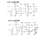
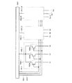
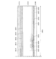
従来のシフトレジスタが有するフリップフロップの構成を図30(A)に示す(特許文献
1)。図30(A)のフリップフロップは、トランジスタ11、トランジスタ12、トラ
ンジスタ13、トランジスタ14、トランジスタ15及びトランジスタ17を有し、信号
線21、信号線22、配線23、信号線24、電源線25、電源線26に接続されている
。信号線21、信号線22、信号線24、電源線25、電源線26には、それぞれスター
ト信号、リセット信号、クロック信号、電源電位VDD、電源電位VSSが入力される。
図30(A)のフリップフロップの動作期間は、図30(B)のタイミングチャートに示
すように、セット期間、選択期間、リセット期間、非選択期間に分割され、動作期間のう
ちのほとんどが非選択期間となる。
Among the internal circuits shown above, a shift register using a transistor formed of an amorphous semiconductor (hereinafter also referred to as an amorphous silicon transistor) has been devised.
A structure of a flip-flop included in a conventional shift register is illustrated in FIG. The flip-flop in FIG. 30A includes a
The operation period of the flip-flop in FIG. 30A is divided into a set period, a selection period, a reset period, and a non-selection period as shown in the timing chart of FIG. Selection period.
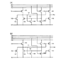
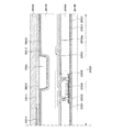
ここで、非選択期間においてトランジスタ12及びトランジスタ16がオンしている。よ
って、トランジスタ12及びトランジスタ16の半導体層にアモルファスシリコンを用い
ているので、劣化等によりしきい値電圧(Vth)に変動が生じる。より具体的には、し
きい値電圧が上昇する。つまり、従来のシフトレジスタは、トランジスタ12及びトラン
ジスタ16のしきい値電圧が上昇してオンできなくなるため、ノード41及び配線23に
VSSを供給することができずに誤動作を起こす。
Here, the
この問題を解決すべく、非特許文献1、非特許文献2及び非特許文献3において、トラン
ジスタ12のしきい値電圧のシフトを抑制できるシフトレジスタが考案されている。非特
許文献1、非特許文献2及び非特許文献3では、新たなトランジスタ(第1のトランジス
タとする)をトランジスタ12(第2のトランジスタとする)と並列に配置し、非選択期
間において、第1のトランジスタのゲート電極及び第2のトランジスタのゲート電極にそ
れぞれ反転した信号を入力することで、第1のトランジスタ及び第2のトランジスタのし
きい値電圧のシフトを抑制している。
In order to solve this problem, Non-Patent
さらに、非特許文献4では、トランジスタ12だけでなく、トランジスタ16のしきい値
電圧のシフトも抑制できるシフトレジスタが考案されている。非特許文献4では、新たな
トランジスタ(第1のトランジスタとする)をトランジスタ12(第2のトランジスタと
する)と並列に配置し、さらに別の新たなトランジスタ(第3のトランジスタとする)を
トランジスタ16(第4のトランジスタとする)と並列に配置する。そして、非選択期間
において、第1のトランジスタのゲート電極及び第2のトランジスタのゲート電極にそれ
ぞれ反転した信号を入力し、第3のトランジスタのゲート電極及び第4のトランジスタの
ゲート電極にそれぞれ反転した信号を入力することで、第1のトランジスタ、第2のトラ
ンジスタ、第3のトランジスタ及び第4のトランジスタのしきい値電圧のシフトを抑制し
ている。
Further,
さらに、非特許文献5では、トランジスタ12のゲート電極に交流パルスを印加すること
で、トランジスタ12のしきい値電圧のシフトを抑制している。
Further, in Non-Patent Document 5, the shift of the threshold voltage of the
なお、非特許文献6及び非特許文献7の表示装置は、アモルファスシリコントランジスタ
で構成されるシフトレジスタを走査線駆動回路として用いて、さらにR、G、Bのサブ画
素に1つの信号線からビデオ信号を入力することで、信号線の数を1/3に減らしている
。こうして、非特許文献6及び非特許文献7の表示装置は、表示パネルとドライバICと
の接続数を減らしている。
Note that the display devices of Non-Patent Document 6 and Non-Patent Document 7 use a shift register formed of an amorphous silicon transistor as a scanning line driver circuit, and further video from one signal line to R, G, and B subpixels. By inputting signals, the number of signal lines is reduced to 1/3. Thus, the display devices of Non-Patent Document 6 and Non-Patent Document 7 reduce the number of connections between the display panel and the driver IC.
従来の技術によれば、劣化しやすいトランジスタのゲートに交流パルスを印加することで
、当該トランジスタのしきい値電圧のシフトを抑制している。しかしながら、トランジス
タの半導体層としてアモルファスシリコンを用いた場合、当然、交流パルスを生成する回
路を構成するトランジスタも、しきい値電圧のシフトを生じてしまうことが問題となる。
According to the conventional technique, the shift of the threshold voltage of the transistor is suppressed by applying an AC pulse to the gate of the transistor that is easily deteriorated. However, when amorphous silicon is used as the semiconductor layer of the transistor, it is a problem that the transistor constituting the circuit that generates the AC pulse also causes a threshold voltage shift.
また、信号線の数を1/3に減らして表示パネルとドライバICとの接点の数を削減する
ことが提案されているが(非特許文献6及び非特許文献7)、実用的にはドライバICの
接点の数をより削減することが求められている。
Further, although it has been proposed to reduce the number of signal lines to 1/3 to reduce the number of contacts between the display panel and the driver IC (Non-Patent Document 6 and Non-Patent Document 7), the driver is practically used. There is a need to further reduce the number of IC contacts.
すなわち従来の技術で解決されないものとして、トランジスタのしきい値電圧の変動を抑
制する回路技術が課題として残されている。表示パネルに実装するドライバICの接点数
を削減する技術が課題として残されている。表示装置の低消費電力化が課題として残され
ている。表示装置の大型化又は高精細化が課題として残されている。
That is, as a problem that cannot be solved by the conventional technique, a circuit technique that suppresses the fluctuation of the threshold voltage of the transistor remains as a problem. A technique for reducing the number of contact points of a driver IC mounted on a display panel remains as a problem. Lowering the power consumption of display devices remains a problem. There remains a problem of enlargement or high definition of the display device.
本明細書で開示する発明は、このような課題の一又は複数を解決することにより産業上有
益な技術を提供することを目的としている。
An object of the invention disclosed in this specification is to provide an industrially useful technique by solving one or more of these problems.
本発明に係わる表示装置は、劣化しやすいトランジスタのゲート電極に、正電源、及び負
電源を交互に印加することによって、当該トランジスタのしきい値電圧のシフトを抑制で
きる。
The display device according to the present invention can suppress a shift in threshold voltage of a transistor by alternately applying a positive power source and a negative power source to a gate electrode of a transistor that is likely to deteriorate.
さらに、本発明に係わる表示装置は、劣化しやすいトランジスタのゲート電極に、スイッ
チを介して高電位(VDD)、またはスイッチを介して低電位(VSS)を、交互に供給
することで、当該トランジスタのしきい値電圧のシフトを抑制できる。
Furthermore, the display device according to the present invention alternately supplies a high potential (VDD) or a low potential (VSS) through a switch to a gate electrode of a transistor that is likely to deteriorate, whereby the transistor The threshold voltage shift can be suppressed.
具体的には、劣化しやすいトランジスタのゲート電極を、第1のスイッチングトランジス
タを介して高電位が供給される配線、及び第2のスイッチングトランジスタを介して低電
位が供給される配線に接続し、第1のスイッチングトランジスタのゲート電極にクロック
信号を入力し、第2のスイッチングトランジスタのゲート電極に反転クロック信号を入力
することで、劣化しやすいトランジスタのゲート電極に高電位、又は低電位を交互に供給
する。
Specifically, the gate electrode of the transistor that is easily deteriorated is connected to a wiring to which a high potential is supplied via the first switching transistor and a wiring to which a low potential is supplied via the second switching transistor, By inputting a clock signal to the gate electrode of the first switching transistor and inputting an inverted clock signal to the gate electrode of the second switching transistor, a high potential or a low potential is alternately applied to the gate electrode of the transistor that is likely to deteriorate. Supply.
なお、本書類(明細書、特許請求の範囲又は図面など)に示すスイッチは、様々な形態の
ものを用いることができる。例としては、電気的スイッチや機械的なスイッチなどがある
。つまり、電流の流れを制御できるものであればよく、特定のものに限定されない。例え
ば、スイッチとして、トランジスタ(例えば、バイポーラトランジスタ、MOSトランジ
スタなど)、ダイオード(例えば、PNダイオード、PINダイオード、ショットキーダ
イオード、MIM(MetalInsulatorMetal)ダイオード、MIS(M
etalInsulatorSemiconductor)ダイオード、ダイオード接続
のトランジスタなど)、サイリスタなどを用いることが出来る。または、これらを組み合
わせた論理回路をスイッチとして用いることが出来る。
Note that a variety of switches can be used as a switch described in this document (specification, claims, drawings, or the like). Examples include electrical switches and mechanical switches. That is, it is only necessary to be able to control the current flow, and is not limited to a specific one. For example, as a switch, a transistor (eg, bipolar transistor, MOS transistor, etc.), a diode (eg, PN diode, PIN diode, Schottky diode, MIM (Metal Insulator Metal) diode, MIS (M
etalInsulatorSemiconductor), a diode-connected transistor, etc.), a thyristor, or the like can be used. Alternatively, a logic circuit combining these can be used as a switch.
スイッチとしてトランジスタを用いる場合、そのトランジスタは、単なるスイッチとして
動作するため、トランジスタの極性(導電型)は特に限定されない。ただし、オフ電流を
抑えたい場合、オフ電流が少ない方の極性のトランジスタを用いることが望ましい。オフ
電流が少ないトランジスタとしては、LDD領域を有するトランジスタやマルチゲート構
造を有するトランジスタ等がある。または、スイッチとして動作させるトランジスタのソ
ース端子の電位が、低電位側電源(Vss、GND、0Vなど)に近い状態で動作する場
合はNチャネル型トランジスタを用いることが望ましい。反対に、ソース端子の電位が、
高電位側電源(Vddなど)に近い状態で動作する場合はPチャネル型トランジスタを用
いることが望ましい。なぜなら、Nチャネル型トランジスタではソース端子が低電位側電
源に近い状態で動作するとき、Pチャネル型トランジスタではソース端子が高電位側電源
に近い状態で動作するとき、ゲートソース間電圧の絶対値を大きくできるため、スイッチ
として、より確実に動作するからである。また、ソースフォロワ動作をしてしまうことが
少ないため、出力電圧の大きさが小さくなってしまうことが少ないからである。
In the case of using a transistor as a switch, the transistor operates as a mere switch, and thus the polarity (conductivity type) of the transistor is not particularly limited. However, when it is desired to suppress off-state current, it is desirable to use a transistor having a polarity with smaller off-state current. As a transistor with low off-state current, there are a transistor having an LDD region, a transistor having a multi-gate structure, and the like. Alternatively, an N-channel transistor is preferably used in the case where the transistor operates as a switch when the potential of the source terminal of the transistor is close to a low-potential power supply (Vss, GND, 0 V, or the like). On the other hand, the potential of the source terminal is
In the case of operating in a state close to a high potential side power source (Vdd or the like), it is desirable to use a P-channel transistor. This is because when the N-channel transistor operates with the source terminal close to the low-potential power supply, and the P-channel transistor operates with the source terminal close to the high-potential power supply, the absolute value of the gate-source voltage is This is because it can be made larger, so that it operates more reliably as a switch. Further, since the source follower operation is rarely performed, the output voltage is rarely reduced.
なお、Nチャネル型トランジスタとPチャネル型トランジスタの両方を用いて、CMOS
型のスイッチをスイッチとして用いてもよい。CMOS型のスイッチにすると、Pチャネ
ル型トランジスタまたはNチャネル型トランジスタのどちらか一方のトランジスタが導通
すれば電流が流れるため、スイッチとして機能しやすくなる。例えば、スイッチへの入力
信号の電圧が高い場合でも、低い場合でも、適切に電圧を出力させることが出来る。さら
に、スイッチをオン・オフさせるための信号の電圧振幅値を小さくすることが出来るので
、消費電力を小さくすることも出来る。
Note that both N-channel and P-channel transistors are used for CMOS.
A type of switch may be used as the switch. When a CMOS switch is used, a current flows when one of the P-channel transistor and the N-channel transistor is turned on, so that the switch can easily function as a switch. For example, the voltage can be appropriately output regardless of whether the voltage of the input signal to the switch is high or low. Further, since the voltage amplitude value of the signal for turning on / off the switch can be reduced, the power consumption can be reduced.
なお、スイッチとしてトランジスタを用いる場合、スイッチは、入力端子(ソース端子ま
たはドレイン端子の一方)と、出力端子(ソース端子またはドレイン端子の他方)と、導
通を制御する端子(ゲート端子)とを有している。一方、スイッチとしてダイオードを用
いる場合、スイッチは、導通を制御する端子を有していない場合がある。そのため、トラ
ンジスタよりもダイオードをスイッチとして用いた方が、端子を制御するための配線を少
なくすることが出来る。
Note that when a transistor is used as a switch, the switch has an input terminal (one of a source terminal or a drain terminal), an output terminal (the other of the source terminal or the drain terminal), and a terminal for controlling conduction (a gate terminal). doing. On the other hand, when a diode is used as the switch, the switch may not have a terminal for controlling conduction. Therefore, the use of a diode as a switch rather than a transistor can reduce the wiring for controlling the terminal.
なお、本明細書において、AとBとが接続されている、と明示的に記載する場合は、Aと
Bとが電気的に接続されている場合と、AとBとが機能的に接続されている場合と、Aと
Bとが直接接続されている場合とを含むものとする。ここで、A、Bは、対象物(例えば
、装置、素子、回路、配線、電極、端子、導電膜、層、など)であるとする。したがって
、本明細書が開示する構成において、所定の接続関係、例えば、図または文章に示された
接続関係に限定されず、図または文章に示された接続関係以外のものも含むものとする。
In this specification, when A and B are explicitly described as being connected, A and B are electrically connected and A and B are functionally connected. And the case where A and B are directly connected. Here, A and B are objects (for example, devices, elements, circuits, wirings, electrodes, terminals, conductive films, layers, etc.). Therefore, the configuration disclosed in this specification is not limited to a predetermined connection relationship, for example, the connection relationship illustrated in the drawing or text, and includes other than the connection relationship illustrated in the drawing or text.
例えば、AとBとが電気的に接続されている場合として、AとBとの電気的な接続を可能
とする素子(例えば、スイッチ、トランジスタ、容量素子、インダクタ、抵抗素子、ダイ
オードなど)が、AとBとの間に1個以上配置されていてもよい。あるいは、AとBとが
機能的に接続されている場合として、AとBとの機能的な接続を可能とする回路(例えば
、論理回路(インバータ、NAND回路、NOR回路など)、信号変換回路(DA変換回
路、AD変換回路、ガンマ補正回路など)、電位レベル変換回路(電源回路(昇圧回路、
降圧回路など)、信号の電位レベルを変えるレベルシフタ回路など)、電圧源、電流源、
切り替え回路、増幅回路(信号振幅または電流量などを大きく出来る回路、オペアンプ、
差動増幅回路、ソースフォロワ回路、バッファ回路など)、信号生成回路、記憶回路、制
御回路など)が、AとBとの間に1個以上配置されていてもよい。あるいは、AとBとが
直接接続されている場合として、AとBとの間に他の素子や他の回路を挟まずに、AとB
とが直接接続されていてもよい。
For example, when A and B are electrically connected, an element (for example, a switch, a transistor, a capacitor, an inductor, a resistance element, a diode, or the like) that enables electrical connection between A and B is provided. 1 or more may be arranged between A and B. Alternatively, when A and B are functionally connected, a circuit (for example, a logic circuit (an inverter, a NAND circuit, a NOR circuit, etc.), a signal conversion circuit that enables functional connection between A and B (DA conversion circuit, AD conversion circuit, gamma correction circuit, etc.), potential level conversion circuit (power supply circuit (boost circuit,
Step-down circuit), level shifter circuit that changes signal potential level), voltage source, current source,
Switching circuit, amplifier circuit (circuit that can increase signal amplitude or current amount, operational amplifier,
One or more differential amplifier circuits, source follower circuits, buffer circuits, etc.), signal generation circuits, memory circuits, control circuits, etc.) may be arranged between A and B. Alternatively, if A and B are directly connected, A and B without interposing another element or other circuit between A and B
And may be directly connected.
なお、AとBとが直接接続されている、と明示的に記載する場合は、AとBとが直接接続
されている場合(つまり、AとBとの間に他の素子や他の回路を間に介さずに接続されて
いる場合)と、AとBとが電気的に接続されている場合(つまり、AとBとの間に別の素
子や別の回路を挟んで接続されている場合)とを含むものとする。
Note that in the case where it is explicitly described that A and B are directly connected, when A and B are directly connected (that is, another element or other circuit between A and B). And A and B are electrically connected (that is, A and B are connected with another element or circuit sandwiched between them). ).
なお、AとBとが電気的に接続されている、と明示的に記載する場合は、AとBとが電気
的に接続されている場合(つまり、AとBとの間に別の素子や別の回路を挟んで接続され
ている場合)と、AとBとが機能的に接続されている場合(つまり、AとBとの間に別の
回路を挟んで機能的に接続されている場合)と、AとBとが直接接続されている場合(つ
まり、AとBとの間に別の素子や別の回路を挟まずに接続されている場合)とを含むもの
とする。つまり、電気的に接続されている、と明示的に記載する場合は、単に、接続され
ている、とのみ明示的に記載されている場合と同じであるとする。
Note that in the case where it is explicitly described that A and B are electrically connected, another element is connected between A and B (that is, another element between A and B). Or when A and B are functionally connected (that is, they are functionally connected with another circuit between A and B). And a case where A and B are directly connected (that is, a case where another element or another circuit is not connected between A and B). That is, when it is explicitly described that it is electrically connected, it is the same as when it is explicitly only described that it is connected.
なお、表示素子、表示素子を有する装置である表示装置、発光素子、発光素子を有する装
置である発光装置は、様々な形態を用いたり、様々な素子を有することが出来る。例えば
、表示素子、表示装置、発光素子または発光装置としては、EL素子(有機EL素子、無
機EL素子又は有機物及び無機物を含むEL素子)、電子放出素子、液晶素子、電子イン
ク、電気泳動素子、グレーティングライトバルブ(GLV)、プラズマディスプレイ(P
DP)、デジタルマイクロミラーデバイス(DMD)、圧電セラミックディスプレイ、カ
ーボンナノチューブ、など、電気磁気的作用により、コントラスト、輝度、反射率、透過
率などが変化する表示媒体を用いることができる。なお、EL素子を用いた表示装置とし
てはELディスプレイ、電子放出素子を用いた表示装置としてはフィールドエミッション
ディスプレイ(FED)やSED方式平面型ディスプレイ(SED:Surface−c
onductionElectron−emitterDisply)など、液晶素子を
用いた表示装置としては液晶ディスプレイ(透過型液晶ディスプレイ、半透過型液晶ディ
スプレイ、反射型液晶ディスプレイ、直視型液晶ディスプレイ、投射型液晶ディスプレイ
)、電子インクや電気泳動素子を用いた表示装置としては電子ペーパーがある。
Note that a display element, a display device that is a device including a display element, a light-emitting element, and a light-emitting device that is a device including a light-emitting element can have various modes or have various elements. For example, as a display element, a display device, a light-emitting element, or a light-emitting device, an EL element (an organic EL element, an inorganic EL element, or an EL element including an organic substance and an inorganic substance), an electron-emitting element, a liquid crystal element, electronic ink, an electrophoretic element, Grating light valve (GLV), plasma display (P
DP, a digital micromirror device (DMD), a piezoelectric ceramic display, a carbon nanotube, and other display media whose contrast, luminance, reflectance, transmittance, and the like change due to an electromagnetic action can be used. An EL display is used as a display device using an EL element, and a field emission display (FED) or a SED type flat display (SED: Surface-c) is used as a display device using an electron-emitting device.
Liquid crystal displays (transmission type liquid crystal display, transflective type liquid crystal display, reflective type liquid crystal display, direct view type liquid crystal display, projection type liquid crystal display), electronic ink, and electrophoresis as display devices using liquid crystal elements such as an inductance Electron-emitter Display There is electronic paper as a display device using an element.
なお、本書類(明細書、特許請求の範囲又は図面など)に記載されたトランジスタとして
、様々な形態のトランジスタを用いることが出来る。よって、用いるトランジスタの種類
に限定はない。例えば、非晶質シリコン、多結晶シリコン、微結晶(マイクロクリスタル
、セミアモルファスとも言う)シリコンなどに代表される非単結晶半導体膜を有する薄膜
トランジスタ(TFT)などを用いることが出来る。TFTを用いる場合、様々なメリッ
トがある。例えば、単結晶シリコンの場合よりも低い温度で製造できるため、製造コスト
の削減、又は製造装置の大型化を図ることができる。製造装置を大きくできるため、大型
基板上に製造できる。そのため、同時に多くの個数の表示装置を製造できるため、低コス
トで製造できる。さらに、製造温度が低いため、耐熱性の弱い基板を用いることができる
。そのため、透明基板上にトランジスタを製造できる。そして、透明な基板上のトランジ
スタを用いて表示素子での光の透過を制御することが出来る。あるいは、トランジスタの
膜厚が薄いため、トランジスタを構成する膜の一部は、光を透過させることが出来る。そ
のため、開口率が向上させることができる。
Note that various types of transistors can be used as the transistor described in this document (the specification, the claims, the drawings, or the like). Thus, there is no limitation on the type of transistor used. For example, a thin film transistor (TFT) including a non-single-crystal semiconductor film typified by amorphous silicon, polycrystalline silicon, microcrystalline (also referred to as semi-amorphous) silicon, or the like can be used. When using TFT, there are various advantages. For example, since manufacturing can be performed at a lower temperature than that of single crystal silicon, manufacturing cost can be reduced or a manufacturing apparatus can be increased in size. Since the manufacturing apparatus can be enlarged, it can be manufactured on a large substrate. Therefore, since a large number of display devices can be manufactured at the same time, it can be manufactured at low cost. Furthermore, since the manufacturing temperature is low, a substrate with low heat resistance can be used. Therefore, a transistor can be manufactured on a transparent substrate. Then, light transmission through the display element can be controlled using a transistor over a transparent substrate. Alternatively, since the thickness of the transistor is small, part of the film included in the transistor can transmit light. Therefore, the aperture ratio can be improved.
なお、多結晶シリコンを製造するときに、触媒(ニッケルなど)を用いることにより、結
晶性をさらに向上させ、電気特性のよいトランジスタを製造することが可能となる。その
結果、ゲートドライバ回路(走査線駆動回路)やソースドライバ回路(信号線駆動回路)
、信号処理回路(信号生成回路、ガンマ補正回路、DA変換回路など)を基板上に一体形
成することが出来る。
Note that by using a catalyst (such as nickel) when manufacturing polycrystalline silicon, it is possible to further improve crystallinity and to manufacture a transistor with favorable electrical characteristics. As a result, a gate driver circuit (scan line driver circuit) and a source driver circuit (signal line driver circuit)
The signal processing circuit (signal generation circuit, gamma correction circuit, DA conversion circuit, etc.) can be integrally formed on the substrate.
なお、微結晶シリコンを製造するときに、触媒(ニッケルなど)を用いることにより、結
晶性をさらに向上させ、電気特性のよいトランジスタを製造することが可能となる。この
とき、レーザーを用いず、熱処理を加えるだけで、結晶性を向上させることができる。そ
の結果、ゲートドライバ回路(走査線駆動回路)やソースドライバ回路の一部(アナログ
スイッチなど)を基板上に一体形成することが出来る。さらに、結晶化のためにレーザー
を用いない場合は、シリコンの結晶性のムラを抑えることができる。そのため、綺麗な画
像を表示することが出来る。
Note that when a microcrystalline silicon is manufactured, by using a catalyst (such as nickel), crystallinity can be further improved and a transistor with favorable electrical characteristics can be manufactured. At this time, crystallinity can be improved only by applying heat treatment without using a laser. As a result, a part of the gate driver circuit (scanning line driver circuit) and the source driver circuit (analog switch or the like) can be integrally formed on the substrate. In addition, when a laser is not used for crystallization, unevenness in crystallinity of silicon can be suppressed. Therefore, a beautiful image can be displayed.
ただし、触媒(ニッケルなど)を用いずに、多結晶シリコンや微結晶シリコンを製造する
ことは可能である。
However, it is possible to produce polycrystalline silicon or microcrystalline silicon without using a catalyst (such as nickel).
または、半導体基板やSOI基板などを用いてトランジスタを形成することが出来る。そ
の場合、MOS型トランジスタ、接合型トランジスタ、バイポーラトランジスタなどを本
明細書に記載されたトランジスタとして用いることが出来る。これらにより、特性やサイ
ズや形状などのバラツキが少なく、電流供給能力が高く、サイズの小さいトランジスタを
製造することができる。これらのトランジスタを用いると、回路の低消費電力化、又は回
路の高集積化を図ることができる。
Alternatively, a transistor can be formed using a semiconductor substrate, an SOI substrate, or the like. In that case, a MOS transistor, a junction transistor, a bipolar transistor, or the like can be used as the transistor described in this specification. Accordingly, a transistor with small variations in characteristics, size, shape, and the like, high current supply capability, and small size can be manufactured. When these transistors are used, low power consumption of the circuit or high integration of the circuit can be achieved.
または、ZnO、a−InGaZnO、SiGe、GaAs、IZO、ITO、SnOな
どの化合物半導体または酸化物半導体を有するトランジスタや、さらに、これらの化合物
半導体または酸化物半導体を薄膜化した薄膜トランジスタなどを用いることが出来る。こ
れらにより、製造温度を低くでき、例えば、室温でトランジスタを製造することが可能と
なる。その結果、耐熱性の低い基板、例えばプラスチック基板やフィルム基板に直接トラ
ンジスタを形成することが出来る。なお、これらの化合物半導体または酸化物半導体を、
トランジスタのチャネル部分に用いるだけでなく、それ以外の用途で用いることも出来る
。例えば、これらの化合物半導体または酸化物半導体を抵抗素子、画素電極、透明電極と
して用いることができる。さらに、それらをトランジスタと同時に成膜又は形成できるた
め、コストを低減できる。
Alternatively, a transistor having a compound semiconductor or an oxide semiconductor such as ZnO, a-InGaZnO, SiGe, GaAs, IZO, ITO, or SnO, or a thin film transistor in which these compound semiconductor or oxide semiconductor is thinned can be used. I can do it. Accordingly, the manufacturing temperature can be lowered, and for example, the transistor can be manufactured at room temperature. As a result, the transistor can be formed directly on a substrate having low heat resistance, such as a plastic substrate or a film substrate. These compound semiconductors or oxide semiconductors are
It can be used not only for the channel portion of the transistor but also for other purposes. For example, these compound semiconductors or oxide semiconductors can be used as resistance elements, pixel electrodes, and transparent electrodes. Furthermore, since these can be formed or formed simultaneously with the transistor, cost can be reduced.
または、インクジェットや印刷法を用いて形成したトランジスタなどを用いることが出来
る。これらにより、室温で製造、低真空度で製造、又は大型基板上に製造することができ
る。また、マスク(レチクル)を用いなくても製造することが可能となるため、トランジ
スタのレイアウトを容易に変更することが出来る。さらに、レジストを用いる必要がない
ので、材料費が安くなり、工程数を削減できる。さらに、必要な部分にのみ膜を付けるた
め、全面に成膜した後でエッチングする、という製法よりも、材料が無駄にならず、低コ
ストにできる。
Alternatively, a transistor formed using an inkjet method or a printing method can be used. By these, it can manufacture at room temperature, manufacture at a low vacuum degree, or can manufacture on a large sized substrate. Further, since the transistor can be manufactured without using a mask (reticle), the layout of the transistor can be easily changed. Furthermore, since it is not necessary to use a resist, the material cost is reduced and the number of processes can be reduced. Further, since a film is formed only on a necessary portion, the material is not wasted and cost can be reduced as compared with a manufacturing method in which etching is performed after film formation on the entire surface.
または、有機半導体やカーボンナノチューブを有するトランジスタ等を用いることができ
る。これらにより、曲げることが可能な基板上にトランジスタを形成することが出来る。
そのため、衝撃に強くできる。
Alternatively, a transistor including an organic semiconductor or a carbon nanotube can be used. Thus, a transistor can be formed over a substrate that can be bent.
Therefore, it can be strong against impact.
その他、様々なトランジスタを用いることができる。 In addition, various transistors can be used.
なお、トランジスタが形成されている基板の種類は、様々なものを用いることができ、特
定のものに限定されることはない。トランジスタが形成される基板としては、例えば、単
結晶基板、SOI基板、ガラス基板、石英基板、プラスチック基板、紙基板、セロファン
基板、石材基板、木材基板、布基板(天然繊維(絹、綿、麻)、合成繊維(ナイロン、ポ
リウレタン、ポリエステル)若しくは再生繊維(アセテート、キュプラ、レーヨン、再生
ポリエステル)などを含む)、皮革基板、ゴム基板、ステンレス・スチル基板、ステンレ
ス・スチル・ホイルを有する基板などを用いることが出来る。あるいは、人などの動物の
皮膚(皮表、真皮)又は皮下組織を基板として用いてもよい。または、ある基板でトラン
ジスタを形成し、その後、別の基板にトランジスタを転置し、別の基板上にトランジスタ
を配置してもよい。トランジスタが転置される基板としては、単結晶基板、SOI基板、
ガラス基板、石英基板、プラスチック基板、紙基板、セロファン基板、石材基板、、木材
基板、布基板(天然繊維(絹、綿、麻)、合成繊維(ナイロン、ポリウレタン、ポリエス
テル)若しくは再生繊維(アセテート、キュプラ、レーヨン、再生ポリエステル)などを
含む)、皮革基板、ゴム基板、ステンレス・スチル基板、ステンレス・スチル・ホイルを
有する基板などを用いることができる。あるいは、人などの動物の皮膚(皮表、真皮)又
は皮下組織を基板として用いてもよい。これらの基板を用いることにより、特性のよいト
ランジスタの形成、消費電力の小さいトランジスタの形成、壊れにくい装置の製造、耐熱
性の付与、又は軽量化を図ることができる。
Note that various types of substrates on which transistors are formed can be used and are not limited to specific types. As a substrate on which a transistor is formed, for example, a single crystal substrate, an SOI substrate, a glass substrate, a quartz substrate, a plastic substrate, a paper substrate, a cellophane substrate, a stone substrate, a wood substrate, a cloth substrate (natural fiber (silk, cotton, hemp) ), Synthetic fibers (including nylon, polyurethane, polyester) or recycled fibers (including acetate, cupra, rayon, recycled polyester), leather substrates, rubber substrates, stainless steel substrates, substrates with stainless steel foil, etc. Can be used. Alternatively, the skin (skin surface, dermis) or subcutaneous tissue of an animal such as a human may be used as the substrate. Alternatively, a transistor may be formed over a certain substrate, and then the transistor may be transferred to another substrate, and the transistor may be disposed over another substrate. As a substrate to which the transistor is transferred, a single crystal substrate, an SOI substrate,
Glass substrate, quartz substrate, plastic substrate, paper substrate, cellophane substrate, stone substrate, wood substrate, cloth substrate (natural fiber (silk, cotton, hemp), synthetic fiber (nylon, polyurethane, polyester) or recycled fiber (acetate, A plastic substrate, a rubber substrate, a stainless steel substrate, a stainless steel substrate, a foil substrate, and the like. Alternatively, the skin (skin surface, dermis) or subcutaneous tissue of an animal such as a human may be used as the substrate. By using these substrates, it is possible to form a transistor with good characteristics, a transistor with low power consumption, manufacture a device that is not easily broken, impart heat resistance, or reduce weight.
なお、トランジスタの構成は、様々な形態をとることができる。特定の構成に限定されな
い。例えば、ゲート電極が2個以上のマルチゲート構造を用いてもよい。マルチゲート構
造にすると、チャネル領域が直列に接続されるため、複数のトランジスタが直列に接続さ
れた構成となる。マルチゲート構造により、オフ電流の低減、トランジスタの耐圧向上に
よる信頼性の向上を図ることができる。あるいは、マルチゲート構造により、飽和領域で
動作する時に、ドレイン・ソース間電圧が変化しても、ドレイン・ソース間電流があまり
変化せず、電圧・電流特性の傾きがフラットな特性にすることができる。電圧・電流特性
の傾きがフラットである特性を利用すると、理想的な電流源回路や、非常に高い抵抗値を
もつ能動負荷を実現することが出来る。その結果、特性のよい差動回路やカレントミラー
回路を実現することが出来る。また、チャネルの上下にゲート電極が配置されている構造
でもよい。チャネルの上下にゲート電極が配置されている構造にすることにより、チャネ
ル領域が増えるため、電流値の増加、、又は空乏層ができやすくなることによるS値の低
減を図ることができる。チャネルの上下にゲート電極が配置されると、複数のトランジス
タが並列に接続されたような構成となる。
Note that the structure of the transistor can take a variety of forms. It is not limited to a specific configuration. For example, a multi-gate structure having two or more gate electrodes may be used. When the multi-gate structure is employed, the channel regions are connected in series, so that a plurality of transistors are connected in series. With the multi-gate structure, the off-state current can be reduced and the reliability can be improved by improving the withstand voltage of the transistor. Or, when operating in the saturation region, the drain-source current does not change much even when the drain-source voltage changes, and the slope of the voltage / current characteristic is flat due to the multi-gate structure. it can. By using the characteristic that the slope of the voltage / current characteristic is flat, an ideal current source circuit and an active load having a very high resistance value can be realized. As a result, a differential circuit or a current mirror circuit with good characteristics can be realized. Alternatively, a structure in which gate electrodes are arranged above and below the channel may be employed. With the structure in which the gate electrodes are arranged above and below the channel, the channel region increases, so that the current value can be increased or the S value can be reduced due to the easy formation of a depletion layer. When gate electrodes are provided above and below a channel, a structure in which a plurality of transistors are connected in parallel is obtained.
あるいは、チャネル領域の上にゲート電極が配置されている構造でもよいし、チャネル領
域の下にゲート電極が配置されている構造でもよい。あるいは、正スタガ構造または逆ス
タガ構造でもよいし、チャネル領域が複数の領域に分かれていてもよいし、チャネル領域
が並列に接続されていてもよいし、チャネル領域が直列に接続されていてもよい。また、
チャネル領域(もしくはその一部)にソース電極やドレイン電極が重なっていてもよい。
チャネル領域(もしくはその一部)にソース電極やドレイン電極が重なる構造にすること
により、チャネル領域の一部に電荷がたまって、動作が不安定になることを防ぐことがで
きる。また、LDD領域を設けても良い。LDD領域を設けることにより、オフ電流の低
減、又はトランジスタの耐圧向上による信頼性の向上を図ることができる。あるいは、L
DD領域を設けることにより、、飽和領域で動作する時に、ドレイン・ソース間電圧が変
化しても、ドレイン・ソース間電流があまり変化せず、電圧・電流特性の傾きがフラット
な特性にすることができる。
Alternatively, a structure in which a gate electrode is disposed over a channel region may be employed, or a structure in which a gate electrode is disposed under a channel region may be employed. Alternatively, a normal stagger structure or an inverted stagger structure may be used, the channel region may be divided into a plurality of regions, the channel regions may be connected in parallel, or the channel regions may be connected in series. Good. Also,
A source electrode or a drain electrode may overlap with the channel region (or a part thereof).
With the structure in which the source electrode or the drain electrode overlaps with the channel region (or part of it), it is possible to prevent electric charges from being accumulated in part of the channel region and unstable operation. Further, an LDD region may be provided. By providing the LDD region, the off-state current can be reduced or the reliability can be improved by improving the withstand voltage of the transistor. Or L
By providing the DD region, when operating in the saturation region, even if the drain-source voltage changes, the drain-source current does not change so much and the slope of the voltage / current characteristic is flat. Can do.
なお、本明細書におけるトランジスタは、様々なタイプを用いることができ、様々な基板
上に形成させることができる。したがって、所定の機能を実現させるために必要な回路の
全てが、同一の基板に形成されていてもよい。例えば、所定の機能を実現させるために必
要な回路の全てが、ガラス基板、プラスチック基板、単結晶基板、またはSOI基板上に
形成されていてもよく、さまざまな基板上に形成されていてもよい。所定の機能を実現さ
せるために必要な回路の全てが同じ基板上に形成されていることにより、部品点数を減ら
してコストを低減し、回路部品との接続点数を減らして信頼性を向上させたりすることが
できる。あるいは、所定の機能を実現させるために必要な回路の一部が、ある基板に形成
されており、所定の機能を実現させるために必要な回路の別の一部が、別の基板に形成さ
れていてもよい。つまり、所定の機能を実現させるために必要な回路の全てが同じ基板上
に形成されていなくてもよい。例えば、所定の機能を実現させるために必要な回路の一部
は、ガラス基板上にトランジスタを用いて形成され、所定の機能を実現させるために必要
な回路の別の一部は、単結晶基板上に形成され、単結晶基板上のトランジスタで構成され
たICチップをCOG(ChipOnGlass)でガラス基板に接続して、ガラス基板
上にそのICチップを配置してもよい。あるいは、そのICチップをTAB(TapeA
utomatedBonding)やプリント基板を用いてガラス基板と接続してもよい
。このように、回路の一部が同じ基板に形成されていることにより、部品点数を減らして
コストを低減し、回路部品との接続点数を減らして信頼性を向上させたりすることができ
る。また、駆動電圧が高い部分や駆動周波数が高い部分の回路は、消費電力が大きくなっ
てしまうので、そのような部分の回路は同じ基板に形成せず、そのかわりに、例えば、単
結晶基板上にその部分の回路を形成して、その回路で構成されたICチップを用いるよう
にすれば、消費電力の増加を防ぐことができる。
Note that various types of transistors can be used in this specification, and the transistor can be formed over various substrates. Therefore, all the circuits necessary for realizing the predetermined function may be formed on the same substrate. For example, all circuits necessary for realizing a predetermined function may be formed over a glass substrate, a plastic substrate, a single crystal substrate, or an SOI substrate, or may be formed over various substrates. . Since all the circuits necessary to realize a given function are formed on the same board, the number of parts can be reduced to reduce costs, and the number of connection points with circuit parts can be reduced to improve reliability. can do. Alternatively, a part of the circuit necessary for realizing the predetermined function is formed on a certain substrate, and another part of the circuit necessary for realizing the predetermined function is formed on another substrate. It may be. That is, not all the circuits necessary for realizing a predetermined function need be formed on the same substrate. For example, a part of a circuit necessary for realizing a predetermined function is formed using a transistor over a glass substrate, and another part of a circuit required for realizing a predetermined function is a single crystal substrate. The IC chip formed on the single crystal substrate and formed of a transistor may be connected to the glass substrate by COG (Chip On Glass), and the IC chip may be arranged on the glass substrate. Alternatively, the IC chip is TAB (Tape A
(automated Bonding) or a printed board may be used to connect to the glass substrate. As described above, since a part of the circuit is formed on the same substrate, the number of parts can be reduced to reduce the cost, and the number of connection points with the circuit parts can be reduced to improve the reliability. In addition, since the power consumption of a circuit having a high driving voltage or a high driving frequency is large, such a circuit is not formed on the same substrate. Instead, for example, on a single crystal substrate. If the circuit of that portion is formed and an IC chip constituted by the circuit is used, an increase in power consumption can be prevented.
なお、本明細書においては、一画素とは、明るさを制御できる要素一つ分を示すものとす
る。よって、一例としては、一画素とは、一つの色要素を示すものとし、その色要素一つ
で明るさを表現する。従って、そのときは、R(赤)G(緑)B(青)の色要素からなる
カラー表示装置の場合には、画像の最小単位は、Rの画素とGの画素とBの画素との三画
素から構成されるものとする。なお、色要素は、三色に限定されず、三色以上を用いても
良いし、RGB以外の色を用いても良い。例えば、白色を加えて、RGBW(Wは白)と
してもよい。また、RGBに、例えば、イエロー、シアン、マゼンタ、エメラルドグリー
ン、朱色などを一色以上追加してもよい。また、例えば、RGBの中の少なくとも一色に
類似した色を、RGBに追加してもよい。例えば、R、G、B1、B2としてもよい。B
1とB2とは、どちらも青色であるが、少し周波数が異なっている。同様に、R1、R2
、G、Bとしてもよい。このような色要素を用いることにより、より実物に近い表示を行
うことができたり、消費電力を低減することが出来る。また、別の例としては、1つの色
要素について、複数の領域を用いて明るさを制御する場合は、その領域一つ分を一画素と
してもよい。よって、一例として、面積階調を行う場合または副画素(サブ画素)を有し
ている場合、一つの色要素につき、明るさを制御する領域が複数あり、その全体で階調を
表現するわけであるが、明るさを制御する領域の一つ分を一画素としてもよい。よって、
その場合は、一つの色要素は、複数の画素で構成されることとなる。あるいは、明るさを
制御する領域が1つの色要素の中に複数あっても、それらをまとめて、1つの色要素を1
画素としてもよい。よって、その場合は、一つの色要素は、一つの画素で構成されること
となる。また、1つの色要素について、複数の領域を用いて明るさを制御する場合、画素
によって、表示に寄与する領域の大きさが異なっている場合がある。また、一つの色要素
につき複数ある、明るさを制御する領域において、各々に供給する信号を僅かに異ならせ
るようにして、視野角を広げるようにしてもよい。つまり、1つの色要素について、複数
個ある領域が各々有する画素電極の電位が、各々異なっていてもよい。その結果、液晶分
子に加わる電圧が各画素電極によって各々異なる。よって、視野角を広くすることが出来
る。
Note that in this specification, one pixel represents one element whose brightness can be controlled. Therefore, as an example, one pixel represents one color element, and brightness is expressed by one color element. Therefore, at that time, in the case of a color display device composed of R (red), G (green), and B (blue) color elements, the minimum unit of an image is an R pixel, a G pixel, and a B pixel. It is assumed to be composed of three pixels. Note that the color elements are not limited to three colors, and three or more colors may be used, or colors other than RGB may be used. For example, RGBW (W is white) may be added by adding white. Further, one or more colors such as yellow, cyan, magenta, emerald green, vermilion, and the like may be added to RGB. Further, for example, a color similar to at least one of RGB may be added to RGB. For example, R, G, B1, and B2 may be used. B
1 and B2 are both blue, but have slightly different frequencies. Similarly, R1, R2
, G, and B may be used. By using such color elements, it is possible to perform display closer to the real thing or to reduce power consumption. As another example, when brightness is controlled using a plurality of areas for one color element, one area may be used as one pixel. Therefore, as an example, when performing area gradation or having sub-pixels (sub-pixels), there are a plurality of brightness control areas for one color element, and the gradation is expressed as a whole. However, one pixel for controlling the brightness may be one pixel. Therefore,
In that case, one color element is composed of a plurality of pixels. Alternatively, even if there are a plurality of areas for controlling the brightness in one color element, they are combined into one color element.
It may be a pixel. Therefore, in that case, one color element is composed of one pixel. When brightness is controlled using a plurality of areas for one color element, the size of the area contributing to display may be different depending on the pixel. In addition, in a plurality of brightness control areas for each color element, the viewing angle may be widened by slightly different signals supplied to each. That is, for one color element, the potentials of the pixel electrodes in each of a plurality of regions may be different from each other. As a result, the voltage applied to the liquid crystal molecules is different for each pixel electrode. Therefore, the viewing angle can be widened.
なお、一画素(三色分)と明示的に記載する場合は、RとGとBの三画素分を一画素と考
える場合であるとする。一画素(一色分)と明示的に記載する場合は、一つの色要素につ
き、複数の領域がある場合、それらをまとめて一画素と考える場合であるとする。
In addition, when it is explicitly described as one pixel (for three colors), it is assumed that three pixels of R, G, and B are considered as one pixel. When it is explicitly described as one pixel (for one color), it is assumed that when there are a plurality of areas for one color element, they are considered as one pixel.
なお、本書類(明細書、特許請求の範囲又は図面など)において、画素は、マトリクス状
に配置(配列)されている場合がある。ここで、画素がマトリクスに配置(配列)されて
いるとは、縦方向もしくは横方向において、画素が直線上に並んで配置されている場合や
、ギザギザな線上に配置されている場合を含む。よって、例えば三色の色要素(例えばR
GB)でフルカラー表示を行う場合に、ストライプ配置されている場合や、三つの色要素
のドットがデルタ配置されている場合も含む。さらに、ベイヤー配置されている場合も含
む。なお、色要素は、三色に限定されず、それ以上でもよく、例えば、RGBW(Wは白
)や、RGBに、イエロー、シアン、マゼンタなどを一色以上追加したものなどがある。
また、色要素のドット毎にその表示領域の大きさが異なっていてもよい。これにより、低
消費電力化、又は表示素子の長寿命化を図ることができる。
Note that in this document (the specification, the claims, the drawings, or the like), the pixels may be arranged (arranged) in a matrix. Here, the pixel being arranged (arranged) in the matrix includes a case where the pixels are arranged in a straight line or a jagged line in the vertical direction or the horizontal direction. Thus, for example, three color elements (for example, R
When full-color display is performed in GB), this includes the case where stripes are arranged and the case where dots of three color elements are arranged in delta. Furthermore, the case where a Bayer is arranged is included. Note that the color elements are not limited to three colors, and may be more than that, for example, RGBW (W is white) or RGB in which one or more colors of yellow, cyan, magenta, etc. are added.
Further, the size of the display area may be different for each dot of the color element. Thereby, it is possible to reduce power consumption or extend the life of the display element.
なお、本書類(明細書、特許請求の範囲又は図面など)において、画素に能動素子を有す
るアクティブマトリクス方式、または、画素に能動素子を有しないパッシブマトリクス方
式を用いることが出来る。
Note that in this document (the specification, the claims, the drawings, and the like), an active matrix method in which an active element is included in a pixel or a passive matrix method in which an active element is not included in a pixel can be used.
アクティブマトリクス方式では、能動素子(アクティブ素子、非線形素子)として、トラ
ンジスタだけでなく、さまざまな能動素子(アクティブ素子、非線形素子)を用いること
が出来る。例えば、MIM(MetalInsulatorMetal)やTFD(Th
inFilmDiode)などを用いることも可能である。これらの素子は、製造工程が
少ないため、製造コストの低減、又は歩留まりの向上を図ることができる。さらに、素子
のサイズが小さいため、開口率を向上させることができ、低消費電力化や高輝度化をはか
ることが出来る。
In the active matrix system, not only transistors but also various active elements (active elements and nonlinear elements) can be used as active elements (active elements and nonlinear elements). For example, MIM (Metal Insulator Metal) or TFD (Th
inFilmDiode) or the like can also be used. Since these elements have few manufacturing processes, manufacturing cost can be reduced or yield can be improved. Further, since the element size is small, the aperture ratio can be improved, and power consumption and luminance can be increased.
なお、アクティブマトリクス方式以外のものとして、能動素子(アクティブ素子、非線形
素子)を用いないパッシブマトリクス型を用いることも可能である。能動素子(アクティ
ブ素子、非線形素子)を用いないため、製造工程が少なく、製造コストの低減、又は歩留
まりの向上を図ることができる。また、能動素子(アクティブ素子、非線形素子)を用い
ないため、開口率を向上させることができ、低消費電力化や高輝度化をはかることが出来
る。
Note that as a method other than the active matrix method, a passive matrix type that does not use an active element (an active element or a nonlinear element) can be used. Since no active element (active element or non-linear element) is used, the number of manufacturing steps is small, and the manufacturing cost can be reduced or the yield can be improved. In addition, since an active element (an active element or a non-linear element) is not used, the aperture ratio can be improved, and low power consumption and high luminance can be achieved.
なお、トランジスタとは、ゲートと、ドレインと、ソースとを含む少なくとも三つの端子
を有する素子であり、ドレイン領域とソース領域の間にチャネル領域を有しており、ドレ
イン領域とチャネル領域とソース領域とを介して電流を流すことが出来る。ここで、ソー
スとドレインとは、トランジスタの構造や動作条件等によって変わるため、いずれがソー
スまたはドレインであるかを限定することが困難である。そこで、本明細書においては、
ソース及びドレインとして機能する領域を、ソースもしくはドレインと呼ばない場合があ
る。その場合、一例としては、それぞれを第1端子、第2端子と表記する場合がある。あ
るいは、それぞれを第1の電極、第2の電極と表記する場合がある。あるいは、ソース領
域、ドレイン領域と表記する場合がある。
Note that a transistor is an element having at least three terminals including a gate, a drain, and a source. The transistor has a channel region between the drain region and the source region, and the drain region, the channel region, and the source region. A current can be passed through. Here, since the source and the drain vary depending on the structure and operating conditions of the transistor, it is difficult to limit which is the source or the drain. Therefore, in this specification,
A region functioning as a source and a drain may not be referred to as a source or a drain. In that case, as an example, there are cases where they are referred to as a first terminal and a second terminal, respectively. Alternatively, each may be referred to as a first electrode and a second electrode. Alternatively, they may be referred to as a source region and a drain region.
なお、トランジスタは、ベースとエミッタとコレクタとを含む少なくとも三つの端子を有
する素子であってもよい。この場合も同様に、エミッタとコレクタとを、第1端子、第2
端子と表記する場合がある。
Note that the transistor may be an element having at least three terminals including a base, an emitter, and a collector. Similarly, in this case, the emitter and collector are connected to the first terminal and the second terminal.
Sometimes referred to as a terminal.
なお、ゲートとは、ゲート電極とゲート配線(ゲート線、ゲート信号線、走査線、走査信
号線等とも言う)とを含んだ全体、もしくは、それらの一部のことを言う。ゲート電極と
は、チャネル領域を形成する半導体と、ゲート絶縁膜を介してオーバーラップしている部
分の導電膜のことを言う。なお、ゲート電極の一部は、LDD(LightlyDope
dDrain)領域またはソース領域とドレイン領域と、ゲート絶縁膜を介してオーバー
ラップしている場合もある。ゲート配線とは、各トランジスタのゲート電極の間を接続す
るための配線、各画素の有するゲート電極の間を接続するための配線、又はゲート電極と
別の配線とを接続するための配線のことを言う。
Note that a gate refers to the whole or part of a gate electrode and a gate wiring (also referred to as a gate line, a gate signal line, a scanning line, a scanning signal line, or the like). A gate electrode refers to a portion of a conductive film which overlaps with a semiconductor forming a channel region with a gate insulating film interposed therebetween. Note that a part of the gate electrode is an LDD (LightlyDope).
dDrain) region or the source region and the drain region may overlap with the gate insulating film. A gate wiring is a wiring for connecting between the gate electrodes of each transistor, a wiring for connecting between the gate electrodes of each pixel, or a wiring for connecting the gate electrode to another wiring. Say.
ただし、ゲート電極としても機能し、ゲート配線としても機能するような部分(領域、導
電膜、配線など)も存在する。そのような部分(領域、導電膜、配線など)は、ゲート電
極と呼んでも良いし、ゲート配線と呼んでも良い。つまり、ゲート電極とゲート配線とが
、明確に区別できないような領域も存在する。例えば、延伸して配置されているゲート配
線の一部とチャネル領域がオーバーラップしている場合、その部分(領域、導電膜、配線
など)はゲート配線として機能しているが、ゲート電極としても機能していることになる
。よって、そのような部分(領域、導電膜、配線など)は、ゲート電極と呼んでも良いし
、ゲート配線と呼んでも良い。
However, there are portions (regions, conductive films, wirings, etc.) that also function as gate electrodes and function as gate wirings. Such a portion (region, conductive film, wiring, or the like) may be called a gate electrode or a gate wiring. That is, there is a region where the gate electrode and the gate wiring cannot be clearly distinguished. For example, when a part of a gate wiring extended and the channel region overlaps, the portion (region, conductive film, wiring, etc.) functions as a gate wiring, but also as a gate electrode It is functioning. Thus, such a portion (region, conductive film, wiring, or the like) may be called a gate electrode or a gate wiring.
なお、ゲート電極と同じ材料で形成され、ゲート電極と同じ島(アイランド)を形成して
つながっている部分(領域、導電膜、配線など)も、ゲート電極と呼んでも良い。同様に
、ゲート配線と同じ材料で形成され、ゲート配線と同じ島(アイランド)を形成してつな
がっている部分(領域、導電膜、配線など)も、ゲート配線と呼んでも良い。このような
部分(領域、導電膜、配線など)は、厳密な意味では、チャネル領域とオーバーラップし
ていない場合、又は別のゲート電極と接続させる機能を有していない場合がある。しかし
、製造工程における条件などの関係で、ゲート電極またはゲート配線と同じ材料で形成さ
れ、ゲート電極またはゲート配線と同じ島(アイランド)を形成してつながっている部分
(領域、導電膜、配線など)がある。よって、そのような部分(領域、導電膜、配線など
)もゲート電極またはゲート配線と呼んでも良い。
Note that a portion (a region, a conductive film, a wiring, or the like) formed using the same material as the gate electrode and connected to form the same island (island) as the gate electrode may be called a gate electrode. Similarly, a portion (a region, a conductive film, a wiring, or the like) formed using the same material as the gate wiring and connected by forming the same island (island) as the gate wiring may be referred to as a gate wiring. In a strict sense, such a portion (region, conductive film, wiring, or the like) may not overlap with the channel region or may not have a function of being connected to another gate electrode. However, due to conditions in the manufacturing process, etc., a portion (region, conductive film, wiring, etc.) that is formed of the same material as the gate electrode or gate wiring and forms the same island (island) as the gate electrode or gate wiring. ) Therefore, such a portion (region, conductive film, wiring, or the like) may also be called a gate electrode or a gate wiring.
なお、例えば、マルチゲートのトランジスタにおいて、1つのゲート電極と、別のゲート
電極とは、ゲート電極と同じ材料で形成された導電膜で接続される場合が多い。そのよう
な部分(領域、導電膜、配線など)は、ゲート電極とゲート電極とを接続させるための部
分(領域、導電膜、配線など)であるため、ゲート配線と呼んでも良いが、マルチゲート
のトランジスタを1つのトランジスタと見なすことも出来るため、ゲート電極と呼んでも
良い。つまり、ゲート電極またはゲート配線と同じ材料で形成され、ゲート電極またはゲ
ート配線と同じ島(アイランド)を形成してつながっている部分(領域、導電膜、配線な
ど)は、ゲート電極やゲート配線と呼んでも良い。さらに、例えば、ゲート電極とゲート
配線とを接続させている部分の導電膜であって、ゲート電極またはゲート配線とは異なる
材料で形成された導電膜も、ゲート電極と呼んでも良いし、ゲート配線と呼んでも良い。
Note that, for example, in a multi-gate transistor, one gate electrode and another gate electrode are often connected to each other with a conductive film formed using the same material as the gate electrode. Such a portion (region, conductive film, wiring, or the like) is a portion (region, conductive film, wiring, or the like) for connecting the gate electrode and the gate electrode, and thus may be referred to as a gate wiring. These transistors can be regarded as a single transistor, and therefore may be referred to as a gate electrode. That is, a portion (a region, a conductive film, a wiring, or the like) that is formed using the same material as the gate electrode or the gate wiring and forms the same island (island) as the gate electrode or the gate wiring is connected to the gate electrode or the gate wiring. You can call it. Further, for example, a conductive film in a portion where the gate electrode and the gate wiring are connected and formed of a material different from the gate electrode or the gate wiring may be referred to as a gate electrode. You may call it.
なお、ゲート端子とは、ゲート電極の部分(領域、導電膜、配線など)または、ゲート電
極と電気的に接続されている部分(領域、導電膜、配線など)について、その一部分のこ
とを言う。
Note that a gate terminal means a part of a part of a gate electrode (a region, a conductive film, a wiring, or the like) or a part electrically connected to the gate electrode (a region, a conductive film, a wiring, or the like). .
なお、ゲート配線、ゲート線、ゲート信号線、走査線、走査信号線などと呼ぶ場合、配線
にトランジスタのゲートが接続されていない場合もある。この場合、ゲート配線、ゲート
線、ゲート信号線、走査線、走査信号線は、トランジスタのゲートと同じ層で形成された
配線、トランジスタのゲートと同じ材料で形成された配線またはトランジスタのゲートと
同時に成膜された配線を意味している場合がある。例としては、保持容量用配線、電源線
、基準電位供給配線などがある。
Note that in the case of calling a gate wiring, a gate line, a gate signal line, a scanning line, a scanning signal line, or the like, the gate of the transistor may not be connected to the wiring. In this case, the gate wiring, the gate line, the gate signal line, the scanning line, and the scanning signal line are formed at the same time as the wiring formed in the same layer as the gate of the transistor, the wiring formed of the same material as the gate of the transistor, or the gate of the transistor. It may mean a deposited wiring. Examples include a storage capacitor wiring, a power supply line, a reference potential supply wiring, and the like.
なお、ソースとは、ソース領域とソース電極とソース配線(ソース線、ソース信号線、デ
ータ線、データ信号線等とも言う)とを含んだ全体、もしくは、それらの一部のことを言
う。ソース領域とは、P型不純物(ボロンやガリウムなど)やN型不純物(リンやヒ素な
ど)が多く含まれる半導体領域のことを言う。従って、少しだけP型不純物やN型不純物
が含まれる領域、いわゆる、LDD(LightlyDopedDrain)領域は、ソ
ース領域には含まれない。ソース電極とは、ソース領域とは別の材料で形成され、ソース
領域と電気的に接続されて配置されている部分の導電層のことを言う。ただし、ソース電
極は、ソース領域も含んでソース電極と呼ぶこともある。ソース配線とは、各トランジス
タのソース電極の間を接続するための配線、各画素の有するソース電極の間を接続するた
めの配線、又はソース電極と別の配線とを接続するための配線のことを言う。
Note that a source refers to the whole or part of a source region, a source electrode, and a source wiring (also referred to as a source line, a source signal line, a data line, a data signal line, or the like). The source region refers to a semiconductor region containing a large amount of P-type impurities (such as boron and gallium) and N-type impurities (such as phosphorus and arsenic). Therefore, a region containing a little P-type impurity or N-type impurity, that is, a so-called LDD (Lightly Doped Drain) region is not included in the source region. A source electrode refers to a portion of a conductive layer which is formed using a material different from that of a source region and is electrically connected to the source region. However, the source electrode may be referred to as a source electrode including the source region. The source wiring is a wiring for connecting the source electrodes of the transistors, a wiring for connecting the source electrodes of each pixel, or a wiring for connecting the source electrode to another wiring. Say.
しかしながら、ソース電極としても機能し、ソース配線としても機能するような部分(領
域、導電膜、配線など)も存在する。そのような部分(領域、導電膜、配線など)は、ソ
ース電極と呼んでも良いし、ソース配線と呼んでも良い。つまり、ソース電極とソース配
線とが、明確に区別できないような領域も存在する。例えば、延伸して配置されているソ
ース配線の一部とソース領域とがオーバーラップしている場合、その部分(領域、導電膜
、配線など)はソース配線として機能しているが、ソース電極としても機能していること
になる。よって、そのような部分(領域、導電膜、配線など)は、ソース電極と呼んでも
良いし、ソース配線と呼んでも良い。
However, there are also portions (regions, conductive films, wirings, etc.) that function as source electrodes and also function as source wirings. Such a portion (region, conductive film, wiring, or the like) may be called a source electrode or a source wiring. That is, there is a region where the source electrode and the source wiring cannot be clearly distinguished. For example, in the case where a part of the source wiring that is arranged to extend and the source region overlap, the portion (region, conductive film, wiring, etc.) functions as the source wiring, but as the source electrode Will also work. Therefore, such a portion (region, conductive film, wiring, or the like) may be called a source electrode or a source wiring.
なお、ソース電極と同じ材料で形成され、ソース電極と同じ島(アイランド)を形成して
つながっている部分(領域、導電膜、配線など)や、ソース電極とソース電極とを接続す
る部分(領域、導電膜、配線など)も、ソース電極と呼んでも良い。さらに、ソース領域
とオーバーラップしている部分も、ソース電極と呼んでも良い。同様に、ソース配線と同
じ材料で形成され、ソース配線と同じ島(アイランド)を形成してつながっている領域も
、ソース配線と呼んでも良い。このような部分(領域、導電膜、配線など)は、厳密な意
味では、別のソース電極と接続させる機能を有していない場合がある。しかし、製造工程
における条件などの関係で、ソース電極またはソース配線と同じ材料で形成され、ソース
電極またはソース配線とつながっている部分(領域、導電膜、配線など)がある。よって
、そのような部分(領域、導電膜、配線など)もソース電極またはソース配線と呼んでも
良い。
Note that a portion (region, conductive film, wiring, or the like) that is formed using the same material as the source electrode and forms the same island (island) as the source electrode, or a portion (region) that connects the source electrode and the source electrode , Conductive film, wiring, etc.) may also be referred to as source electrodes. Further, a portion overlapping with the source region may be called a source electrode. Similarly, a region formed of the same material as the source wiring and connected by forming the same island (island) as the source wiring may be called a source wiring. Such a portion (region, conductive film, wiring, or the like) may not have a function of connecting to another source electrode in a strict sense. However, there is a portion (a region, a conductive film, a wiring, or the like) that is formed using the same material as the source electrode or the source wiring and connected to the source electrode or the source wiring because of conditions in the manufacturing process. Therefore, such a portion (region, conductive film, wiring, or the like) may also be called a source electrode or a source wiring.
なお、例えば、ソース電極とソース配線とを接続させている部分の導電膜であって、ソー
ス電極またはソース配線とは異なる材料で形成された導電膜も、ソース電極と呼んでも良
いし、ソース配線と呼んでも良い。
Note that, for example, a conductive film in a portion where the source electrode and the source wiring are connected and formed using a material different from that of the source electrode or the source wiring may be referred to as a source electrode or a source wiring. You may call it.
なお、ソース端子とは、ソース領域の領域や、ソース電極や、ソース電極と電気的に接続
されている部分(領域、導電膜、配線など)について、その一部分のことを言う。
Note that a source terminal refers to a part of a source region, a source electrode, or a portion (region, conductive film, wiring, or the like) electrically connected to the source electrode.
なお、ソース配線、ソース線、ソース信号線、データ線、データ信号線などと呼ぶ場合、
配線にトランジスタのソース(ドレイン)が接続されていない場合もある。この場合、ソ
ース配線、ソース線、ソース信号線、データ線、データ信号線は、トランジスタのソース
(ドレイン)と同じ層で形成された配線、トランジスタのソース(ドレイン)と同じ材料
で形成された配線またはトランジスタのソース(ドレイン)と同時に成膜された配線を意
味している場合がある。例としては、保持容量用配線、電源線、基準電位供給配線などが
ある。
In addition, when calling a source wiring, a source line, a source signal line, a data line, a data signal line, etc.
In some cases, the source (drain) of the transistor is not connected to the wiring. In this case, the source wiring, the source line, the source signal line, the data line, and the data signal line are a wiring formed of the same layer as the source (drain) of the transistor and a wiring formed of the same material as the source (drain) of the transistor. Alternatively, it may mean a wiring formed simultaneously with the source (drain) of the transistor. Examples include a storage capacitor wiring, a power supply line, a reference potential supply wiring, and the like.
なお、ドレインについては、ソースと同様である。 The drain is the same as the source.
なお、半導体装置とは半導体素子(トランジスタ、ダイオード、サイリスタなど)を含む
回路を有する装置のことをいう。さらに、半導体特性を利用することで機能しうる装置全
般を半導体装置と呼んでもよい。
Note that a semiconductor device refers to a device having a circuit including a semiconductor element (a transistor, a diode, a thyristor, or the like). Furthermore, a device that can function by utilizing semiconductor characteristics may be called a semiconductor device.
なお、表示素子とは、光学変調素子、液晶素子、発光素子、EL素子(有機EL素子、無
機EL素子又は有機物及び無機物を含むEL素子)、電子放出素子、電気泳動素子、放電
素子、光反射素子、光回折素子、デジタルマイクロミラーデバイス(DMD)、などのこ
とを言う。ただし、これに限定されない。
Note that a display element means an optical modulation element, a liquid crystal element, a light emitting element, an EL element (an organic EL element, an inorganic EL element or an EL element containing an organic substance and an inorganic substance), an electron-emitting element, an electrophoretic element, a discharge element, and a light reflection element. An element, a light diffraction element, a digital micromirror device (DMD), etc. are said. However, it is not limited to this.
なお、表示装置とは、表示素子を有する装置のことを言う。なお、表示装置とは、表示素
子を含む複数の画素またはそれらの画素を駆動させる周辺駆動回路が同一基板上に形成さ
れた表示パネル本体のことでもよい。なお、表示装置は、ワイヤボンディングやバンプな
どによって基板上に配置された周辺駆動回路、いわゆる、チップオングラス(COG)で
接続されたICチップ、または、TABなどで接続されたICチップを含んでいても良い
。なお、表示装置は、ICチップ、抵抗素子、容量素子、インダクタ、トランジスタなど
が取り付けられたフレキシブルプリントサーキット(FPC)を含んでもよい。なお、表
示装置は、フレキシブルプリントサーキット(FPC)などを介して接続され、ICチッ
プ、抵抗素子、容量素子、インダクタ、トランジスタなどが取り付けられたプリント配線
基盤(PWB)を含んでいても良い。なお、表示装置は、偏光板または位相差板などの光
学シートを含んでいても良い。なお、表示装置は、照明装置、筐体、音声入出力装置、光
センサなどを含んでいても良い。ここで、バックライトユニットのような照明装置は、導
光板、プリズムシート、拡散シート、反射シート、光源(LED、冷陰極管など)、冷却
装置(水冷式、空冷式)などを含んでいても良い。
Note that a display device refers to a device having a display element. Note that the display device may be a display panel body in which a plurality of pixels including display elements or a peripheral drive circuit for driving the pixels is formed over the same substrate. Note that the display device includes a peripheral drive circuit arranged on the substrate by wire bonding or bumps, an IC chip connected by so-called chip-on-glass (COG), or an IC chip connected by TAB or the like. May be. Note that the display device may include a flexible printed circuit (FPC) to which an IC chip, a resistor, a capacitor, an inductor, a transistor, and the like are attached. Note that the display device may include a printed wiring board (PWB) connected via a flexible printed circuit (FPC) or the like to which an IC chip, a resistor element, a capacitor element, an inductor, a transistor, or the like is attached. Note that the display device may include an optical sheet such as a polarizing plate or a retardation plate. Note that the display device may include a lighting device, a housing, a voice input / output device, an optical sensor, and the like. Here, the illumination device such as the backlight unit may include a light guide plate, a prism sheet, a diffusion sheet, a reflection sheet, a light source (LED, cold cathode tube, etc.), a cooling device (water cooling type, air cooling type) and the like. good.
なお、照明装置は、バックライトユニット、導光板、プリズムシート、拡散シート、反射
シート、光源(LED、冷陰極管、熱陰極管など)、冷却装置などを有している装置のこ
とをいう。
Note that the lighting device refers to a device including a backlight unit, a light guide plate, a prism sheet, a diffusion sheet, a reflective sheet, a light source (such as an LED, a cold cathode tube, a hot cathode tube), a cooling device, and the like.
なお、発光装置とは、発光素子などを有している装置のことをいう。 Note that a light-emitting device refers to a device having a light-emitting element or the like.
なお、反射装置とは、光反射素子、光回折素子、光反射電極などを有している装置のこと
をいう。
The reflection device refers to a device having a light reflection element, a light diffraction element, a light reflection electrode, and the like.
なお、液晶表示装置とは、液晶素子を有している表示装置をいう。液晶表示装置には、直
視型、投写型、透過型、反射型、半透過型などがある。
Note that a liquid crystal display device refers to a display device having a liquid crystal element. Liquid crystal display devices include direct view type, projection type, transmission type, reflection type, and transflective type.
なお、駆動装置とは、半導体素子、電気回路、電子回路を有する装置のことを言う。例え
ば、ソース信号線から画素内への信号の入力を制御するトランジスタ(選択用トランジス
タ、スイッチング用トランジスタなどと呼ぶことがある)、画素電極に電圧または電流を
供給するトランジスタ、発光素子に電圧または電流を供給するトランジスタなどは、駆動
装置の一例である。さらに、ゲート信号線に信号を供給する回路(ゲートドライバ、ゲー
ト線駆動回路などと呼ぶことがある)、ソース信号線に信号を供給する回路(ソースドラ
イバ、ソース線駆動回路などと呼ぶことがある)などは、駆動装置の一例である。
Note that a driving device refers to a device having a semiconductor element, an electric circuit, and an electronic circuit. For example, a transistor that controls input of a signal from a source signal line into a pixel (sometimes referred to as a selection transistor or a switching transistor), a transistor that supplies voltage or current to a pixel electrode, or a voltage or current to a light-emitting element A transistor that supplies the voltage is an example of a driving device. Further, a circuit for supplying a signal to the gate signal line (sometimes referred to as a gate driver or a gate line driver circuit) and a circuit for supplying a signal to the source signal line (sometimes referred to as a source driver or source line driver circuit). ) Is an example of a driving device.
なお、表示装置、半導体装置、照明装置、冷却装置、発光装置、反射装置、駆動装置など
は、互いに重複して有している場合がある。例えば、表示装置が、半導体装置および発光
装置を有している場合がある。あるいは、半導体装置が、表示装置および駆動装置を有し
ている場合がある。
Note that a display device, a semiconductor device, a lighting device, a cooling device, a light-emitting device, a reflecting device, a driving device, and the like may overlap with each other. For example, the display device may include a semiconductor device and a light-emitting device. Alternatively, the semiconductor device may include a display device and a driving device.
なお、本書類(明細書、特許請求の範囲又は図面など)において、Aの上にBが形成され
ている、あるいは、A上にBが形成されている、と明示的に記載する場合は、Aの上にB
が直接接して形成されていることに限定されない。直接接してはいない場合、つまり、A
とBと間に別の対象物が介在する場合も含むものとする。ここで、A、Bは、対象物(例
えば、装置、素子、回路、配線、電極、端子、導電膜、層、など)であるとする。
In addition, in this document (specifications, claims, drawings, etc.), if it is explicitly stated that B is formed on A or B is formed on A, B on A
Is not limited to being formed in direct contact. If not in direct contact, that is, A
And a case where another object is interposed between B and B. Here, A and B are objects (for example, devices, elements, circuits, wirings, electrodes, terminals, conductive films, layers, etc.).
従って例えば、層Aの上に(もしくは層A上に)、層Bが形成されている、と明示的に記
載されている場合は、層Aの上に直接接して層Bが形成されている場合と、層Aの上に直
接接して別の層(例えば層Cや層Dなど)が形成されていて、その上に直接接して層Bが
形成されている場合とを含むものとする。なお、別の層(例えば層Cや層Dなど)は、単
層でもよいし、複層でもよい。
Therefore, for example, when it is explicitly described that the layer B is formed on the layer A (or on the layer A), the layer B is formed in direct contact with the layer A. And the case where another layer (for example, layer C or layer D) is formed in direct contact with the layer A, and the layer B is formed in direct contact therewith. Note that another layer (for example, the layer C or the layer D) may be a single layer or a multilayer.
さらに、Aの上方にBが形成されている、と明示的に記載されている場合についても同様
であり、Aの上にBが直接接していることに限定されず、AとBとの間に別の対象物が介
在する場合も含むものとする。従って例えば、層Aの上方に、層Bが形成されている、と
いう場合は、層Aの上に直接接して層Bが形成されている場合と、層Aの上に直接接して
別の層(例えば層Cや層Dなど)が形成されていて、その上に直接接して層Bが形成され
ている場合とを含むものとする。なお、別の層(例えば層Cや層Dなど)は、単層でもよ
いし、複層でもよい。
Furthermore, the same applies to the case where B is explicitly described as being formed above A, and is not limited to the direct contact of B on A. This includes the case where another object is interposed in. Therefore, for example, when the layer B is formed above the layer A, the case where the layer B is formed in direct contact with the layer A and the case where another layer is formed in direct contact with the layer A. (For example, the layer C or the layer D) is formed, and the layer B is formed in direct contact therewith. Note that another layer (for example, the layer C or the layer D) may be a single layer or a multilayer.
なお、Aの上にBが直接接して形成されている、と明示的に記載する場合は、Aの上に直
接接してBが形成されている場合を含み、AとBと間に別の対象物が介在する場合は含ま
ないものとする。
In addition, when it is explicitly described that B is formed in direct contact with A, it includes a case in which B is formed in direct contact with A. It shall not be included when an object is present.
なお、Aの下にBが、あるいは、Aの下方にBが、の場合についても、同様である。 The same applies to the case where B is below A or B is below A.
本明細書によって、シフトレジスタが有する全てのトランジスタの特性劣化を抑制するこ
とができる。そのため、液晶表示装置をはじめとする当該シフトレジスタを適用した半導
体装置の誤動作を抑制することができる。
According to this specification, deterioration of characteristics of all transistors included in the shift register can be suppressed. Therefore, malfunction of a semiconductor device to which the shift register such as a liquid crystal display device is applied can be suppressed.
以下、本発明の実施の形態について図面を参照しながら説明する。但し、本発明は多くの
異なる態様で実施することが可能であり、本発明の趣旨及びその範囲から逸脱することな
くその形態及び詳細を様々に変更し得ることは当業者であれば容易に理解される。従って
本実施の形態の記載内容に限定して解釈されるものではない。
Hereinafter, embodiments of the present invention will be described with reference to the drawings. However, the present invention can be implemented in many different modes, and those skilled in the art can easily understand that the modes and details can be variously changed without departing from the spirit and scope of the present invention. Is done. Therefore, the present invention is not construed as being limited to the description of this embodiment mode.
(実施の形態1)
本実施の形態では、フリップフロップ、当該フリップフロップを有する駆動回路、及び当
該駆動回路を有する表示装置の構成並びに駆動方法について説明する。
(Embodiment 1)
In this embodiment, a structure and a driving method of a flip-flop, a driver circuit including the flip-flop, and a display device including the driver circuit are described.
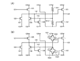
本実施の形態のフリップフロップの基本構成について、図1(A)を参照して説明する。
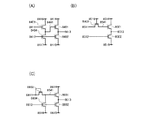
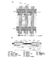
図1(A)に示すフリップフロップは、第1のトランジスタ101、第2のトランジスタ
102、第3のトランジスタ103、第4のトランジスタ104、第5のトランジスタ1
05、第6のトランジスタ106、第7のトランジスタ107及び第8のトランジスタ1
08を有する。本実施の形態において、第1のトランジスタ101〜第8のトランジスタ
108は、Nチャネル型トランジスタとし、ゲートとソース間電圧(Vgs)がしきい値
電圧(Vth)を上回ったとき導通状態になるものとする。
A basic structure of the flip-flop of this embodiment is described with reference to FIG.
The flip-flop illustrated in FIG. 1A includes a
05,
08. In this embodiment, the
なお、本実施の形態のフリップフロップは、第1のトランジスタ101〜第8のトランジ
スタ108が全てNチャネル型トランジスタで構成されていることを特徴とする。したが
って、本実施の形態のフリップフロップは、トランジスタの半導体層として、アモルファ
スシリコンを用いることができるため、製造工程の簡略化を図ることができ、製造コスト
の削減や歩留まりの向上を図ることができる。ただし、トランジスタの半導体層として、
ポリシリコンや多結晶シリコンを用いても製造工程の簡略化を図ることができる。
Note that the flip-flop of this embodiment is characterized in that the
Even if polysilicon or polycrystalline silicon is used, the manufacturing process can be simplified.
図1(A)のフリップフリップフロップの接続関係について説明する。第1のトランジス
タ101の第1の電極(ソース電極及びドレイン電極の一方)が第5の配線125に接続
され、第1のトランジスタ101の第2の電極(ソース電極及びドレイン電極の他方)が
第3の配線123に接続される。第2のトランジスタ102の第1の電極が第4の配線1
24に接続され、第2のトランジスタ102第2の電極が第3の配線123に接続され、
第2のトランジスタ102のゲート電極が第8の配線128に接続される。第3のトラン
ジスタ103の第1の電極が第6の配線126に接続され、第3のトランジスタ103の
第2の電極が第6のトランジスタ106のゲート電極に接続され、第3のトランジスタ1
03のゲート電極が第7の配線127に接続される。第4のトランジスタ104の第1の
電極が第10の配線130に接続され、第4のトランジスタ104の第2の電極が第6の
トランジスタ106のゲート電極に接続され、第4のトランジスタ104のゲート電極が
第8の配線128に接続される。第5のトランジスタ105の第1の電極が第9の配線1
29に接続され、第5のトランジスタ105の第2の電極が第1のトランジスタ101の
ゲート電極に接続され、第5のトランジスタ105のゲート電極が第1の配線121に接
続される。第6のトランジスタ106の第1の電極が第12の配線132に接続され、第
6のトランジスタ106の第2の電極が第1のトランジスタ101のゲート電極に接続さ
れる。第7のトランジスタ107の第1の電極が第13の配線133に接続され、第7の
トランジスタ107の第2の電極が第1のトランジスタ101のゲート電極に接続され、
第7のトランジスタ107のゲート電極が第2の配線122に接続される。第8のトラン
ジスタ108の第1の電極が第11の配線131に接続され、第8のトランジスタ108
の第2の電極が第6のトランジスタ106のゲート電極に接続され、第8のトランジスタ
108のゲート電極が第1のトランジスタ101のゲート電極に接続される。
A connection relation of the flip-flop of FIG. The first electrode (one of the source electrode and the drain electrode) of the
24, the second electrode of the
A gate electrode of the
The gate electrode 03 is connected to the
29, the second electrode of the
A gate electrode of the
The second electrode is connected to the gate electrode of the
なお、第1のトランジスタ101のゲート電極、第6のトランジスタ106の第2の電極
、第7のトランジスタ107の第2の電極及び第8のトランジスタ108のゲート電極の
接続箇所をノード141とする。さらに、第3のトランジスタ103の第2の電極、第4
のトランジスタ104の第2の電極、第6のトランジスタ106のゲート電極及び第8の
トランジスタ108の第2の電極の接続箇所をノード142とする。
Note that a connection position of the gate electrode of the
A connection portion of the second electrode of the
なお、第1の配線121、第2の配線122、第3の配線123、第5の配線125、第
7の配線127及び第8の配線128を、それぞれ第1の信号線、第2の信号線、第3の
信号線、第4の信号線、第5の信号線、第6の信号線と呼んでもよい。さらに、第4の配
線124、第6の配線126、第9の配線129、第10の配線130、第11の配線1
31、第12の配線132及び第13の配線133を、それぞれ第1の電源線、第2の電
源線、第3の電源線、第4の電源線、第5の電源線、第6の電源線、第7の電源線と呼ん
でもよい。
Note that the
31, the
次に、図1(A)に示したフリップフロップの動作について、図2のタイミングチャート
、図3及び図4を参照して説明する。さらに、図2のタイミングチャートをセット期間、
選択期間、リセット期間、第1の非選択期間、第2の非選択期間に分割して説明する。た
だし、セット期間、リセット期間、第1の非選択期間及び第2の非選択期間を合わせて非
選択期間と呼ぶこともある。
Next, operation of the flip-flop illustrated in FIG. 1A is described with reference to a timing chart of FIG. 2 and FIGS. 3 and 4. Furthermore, the timing chart of FIG.
The description will be divided into a selection period, a reset period, a first non-selection period, and a second non-selection period. However, the set period, the reset period, the first non-selection period, and the second non-selection period may be collectively referred to as a non-selection period.
なお、第6の配線126及び第9の配線129にはV1の電位が供給され、第4の配線1
24、第10の配線130、第11の配線131、第12の配線132及び第13の配線
133にはV2の電位が供給される。ここで、V1>V2である。
Note that the
24, the potential of V2 is supplied to the
なお、第1の配線121、第5の配線125、第8の配線128、第7の配線127及び
第2の配線122には、それぞれ図2に示す信号221、信号225、信号228、信号
227、信号222が入力される。そして、第3の配線123からは、図2に示す信号2
23が出力される。ここで、信号221、信号225、信号228、信号227、信号2
22及び信号223は、H信号の電位がV1(以下、Hレベルともいう)、L信号の電位
がV2(以下、Lレベルともいう)のデジタル信号である。さらに、信号221、信号2
25、信号228、信号227、信号222及び信号223を、それぞれスタート信号、
パワークロック信号(PCK)、第1の制御クロック信号(CCK1)、第2の制御クロ
ック信号(CCK2)、リセット信号、出力信号と呼んでもよい。
Note that the
23 is output. Here, signal 221, signal 225, signal 228, signal 227,
22 and the
25, signal 228, signal 227, signal 222 and signal 223, respectively, start signal,
You may call a power clock signal (PCK), a 1st control clock signal (CCK1), a 2nd control clock signal (CCK2), a reset signal, and an output signal.
ただし、第1の配線121、第2の配線122、第4の配線124〜第13の配線133
には、それぞれ様々な信号、電位及び電流が入力されてもよい。
However, the
Various signals, potentials, and currents may be input to each.
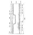
まず、図2(A)及び図3(A)に示すセット期間において、信号221がHレベルとな
り第5のトランジスタ105がオンし、信号222がLレベルなので第7のトランジスタ
107がオフし、信号228がHレベルとなり第2のトランジスタ102及び第4のトラ
ンジスタ104がオンし、信号227がLレベルとなり第3のトランジスタ103がオフ
する。このときのノード141の電位(電位241)は、第5のトランジスタ105の第
2の電極がソース電極となって、第9の配線129の電位から第5のトランジスタ105
のしきい値電圧を引いた値となるためV1−Vth105(Vth105:第5のトラン
ジスタ105のしきい値電圧)となる。よって、第1のトランジスタ101及び第8のト
ランジスタ108がオンし、第5のトランジスタ105がオフする。このときのノード1
42の電位(電位242)は、V2となって、第6のトランジスタ106がオフする。こ
のように、セット期間では、第3の配線123はL信号が入力される第5の配線125及
びV2が供給される第4の配線124と導通するため、第3の配線123の電位がV2と
なる。したがって、L信号が第3の配線123から出力される。さらに、ノード141は
、電位をV1−Vth105に維持したまま浮遊状態となる。
First, in the set period shown in FIGS. 2A and 3A, the
Therefore, V1-Vth105 (Vth105: threshold voltage of the fifth transistor 105) is obtained. Accordingly, the
The potential 42 (potential 242) becomes V2, and the
なお、本実施の形態のフリップフロップは、図5(A)に示すように、第5のトランジス
タ105の第1の電極が第1の配線121に接続されても、上記説明したセット期間と同
様な動作を行うことができる。図5(A)のフリップフロップは、第9の配線129が不
要となるため、歩留まりの向上を図ることができる。さらに、図5(A)のフリップフロ
ップは、レイアウト面積の縮小を図ることができる。
Note that as shown in FIG. 5A, the flip-flop of this embodiment mode is similar to the above-described set period even when the first electrode of the
なお、本実施の形態のフリップフロップは、図5(C)に示すように、トランジスタ50
1を新たに配置してもよい。トランジスタ501は第1の電極がV2が供給されている配
線511に接続され、第2の電極がノード141に接続され、ゲート電極が第1の配線1
21に接続される。図5(C)のフリップフロップは、トランジスタ501によって、ノ
ード142の電位が下がる時間を短くできるので、第6のトランジスタ106を早くオフ
できる。したがって、図5(C)のフリップフロップは、ノード141の電位がV1−V
th105となるまでの時間を短くできるため、高速動作が可能となり、より大型の表示
装置又はより高精細な表示装置に適用できる。
Note that the flip-flop of this embodiment includes a transistor 50 as illustrated in FIG.
1 may be newly arranged. The transistor 501 has a first electrode connected to the wiring 511 to which V2 is supplied, a second electrode connected to the
21. In the flip-flop in FIG. 5C, the time during which the potential of the
Since the time to reach th105 can be shortened, high-speed operation is possible, and it can be applied to a larger display device or a higher definition display device.
図2(B)及び図3(B)に示す選択期間では、信号221がLレベルとなり第5のトラ
ンジスタ105がオフし、信号222がLレベルのままなので第7のトランジスタ107
がオフのままであり、信号228がLレベルとなり第2のトランジスタ102及び第4の
トランジスタ104がオフし、信号227がHレベルとなり第3のトランジスタ103が
オンする。このときのノード141は電位をV1−Vth105に維持している。よって
、第1のトランジスタ101及び第8のトランジスタ108はオンのままである。このと
きのノード142の電位は、第11の配線131の電位(V2)と第6の配線126の電
位(V1)との電位差(V1−V2)が第3のトランジスタ103及び第8のトランジス
タ108によって分圧され、V2+β(β:任意の正の数)となる。さらに、β<Vth
106(第6のトランジスタ106のしきい値電圧)とする。よって第6のトランジスタ
106がオフのままである。ここで、第5の配線125にH信号が入力されるので、第3
の配線123の電位が上昇し始める。すると、ノード141の電位は、ブートストラップ
動作によってV1−Vth105から上昇し、V1+Vth101+α(Vth101:
第1のトランジスタ101のしきい値電圧、α:任意の正の数)となる。したがって、第
3の配線123の電位は、第5の配線125と等しい電位となるのでV1となる。このよ
うに、選択期間では、第3の配線123はH信号が入力されている第5の配線125と導
通するため、第3の配線123の電位がV1となる。したがって、H信号が第3の配線1
23から出力される。
In the selection period illustrated in FIGS. 2B and 3B, the
Remains off, the
106 (the threshold voltage of the sixth transistor 106). Accordingly, the
The potential of the
The threshold voltage of the
23.
なお、このブートストラップ動作は、第1のトランジスタ101のゲート電極と第2の電
極との間の寄生容量の容量結合によって行われる。ただし、図1(B)に示すように、第
1のトランジスタ101のゲート電極と第2の電極との間に容量素子151を配置するこ
とで、安定してブートストラップ動作を行うことができ、第1のトランジスタ101の寄
生容量を小さくできる。ここで、容量素子151は、絶縁層としてゲート絶縁膜を用いて
導電層としてゲート電極層及び配線層を用いてもよいし、絶縁層としてゲート絶縁膜を用
いて導電層としてゲート電極層及び不純物が添加された半導体層を用いてもよいし、絶縁
層として層間膜(絶縁膜)を用いて導電層として配線層及び透明電極層を用いてもよい。
ただし、容量素子151は、導電膜としてゲート電極層及び配線層を用いる場合、ゲート
電極層を第1のトランジスタ101のゲート電極と接続し、配線層を第1のトランジスタ
101の第2の電極と接続するとよい。より望ましくは、導電膜としてゲート電極層及び
配線層を用いる場合、ゲート電極層を第1のトランジスタ101のゲート電極と直接接続
し、配線層を第1のトランジスタ101の第2の電極と直接接続するとよい。なぜなら、
容量素子151の配置によるフリップフロップのレイアウト面積の増加が小さくなるから
である。
Note that this bootstrap operation is performed by capacitive coupling of parasitic capacitance between the gate electrode and the second electrode of the
However, in the
This is because the increase in the layout area of the flip-flop due to the arrangement of the
さらに、図1(C)に示すように、容量素子151としてトランジスタ152を用いても
よい。トランジスタ152は、ゲート電極がノード141に接続され、第1の電極及び第
2の電極が第3の配線123に接続されることで、大きな容量成分を持つ容量素子として
機能することができる。ただし、トランジスタ152は、第1の電極及び第2の電極のう
ちどちらか一方を浮遊としても容量素子として機能できる。
Further, a
なお、第1のトランジスタ101は、第3の配線123にH信号を供給しなければならな
い。したがって、信号223の立ち下がり時間及び立ち上がり時間を短くするために、第
1のトランジスタ101のW/Lの値は、第1のトランジスタ101〜第8のトランジス
タ108のそれぞれのW/Lの値の中で最大とすることが望ましい。
Note that the
さらに、第5のトランジスタ105は、セット期間において、ノード142(第1のトラ
ンジスタ101のゲート電極)の電位をV1−Vth105としなれければならないため
、第5のトランジスタ105のW/Lの値は第1のトランジスタ101のW/Lの値より
も1/2倍〜1/5倍、より望ましくは1/3倍〜1/4倍とする。
Further, in the
なお、ノード142の電位をV2+βとするために、第8のトランジスタ108のチャネ
ル幅Wとチャネル長Lとの比W/Lの値は、第3のトランジスタ103のW/Lの値より
も、少なくとも10倍以上にすることが好ましい。したがって、第8のトランジスタ10
8のトランジスタサイズ(W×L)が大きくなってしまう。ここで、第3のトランジスタ
103のチャネル長Lの値を第8のトランジスタ108のチャネル長Lの値よりも大きく
、より好ましくは2倍〜3倍とすることで、第8のトランジスタ108のトランジスタサ
イズを小さくできるため、レイアウト面積の縮小を図ることができる。
Note that in order to set the potential of the
8 transistor size (W × L) becomes large. Here, the value of the channel length L of the
図2(C)及び図3(C)に示すリセット期間では、信号221がLレベルのままなので
第5のトランジスタ105がオフのままであり、信号222がHレベルとなり第7のトラ
ンジスタ107がオンし、信号228がHレベルとなり第2のトランジスタ102及び第
4のトランジスタ104がオンし、信号227がLレベルとなり第3のトランジスタ10
3がオフする。このときのノード141の電位は、第13の配線133の電位(V2)が
第7のトランジスタ107を介して供給されるためV2となる。よって、第1のトランジ
スタ101及び第8のトランジスタ108がオフする。このときのノード142の電位は
、第4のトランジスタ104がオンするので、V2となる。よって、第6のトランジスタ
106がオフする。このように、リセット期間では、第3の配線123はV2が供給され
ている第4の配線124と導通するため、第3の配線123の電位がV2となる。したが
って、L信号が第3の配線123から出力される。
In the reset period illustrated in FIGS. 2C and 3C, since the
3 turns off. The potential of the
なお、第7のトランジスタ107がオンするタイミングを遅延させることで、信号223
の立ち下がり時間を短くできる。なぜなら、第5の配線125に入力されるL信号が、W
/Lの値が大きい第1のトランジスタ101を介して第3の配線123に供給できるから
である。
Note that the
The fall time can be shortened. This is because the L signal input to the
This is because the voltage can be supplied to the
あるいは、第7のトランジスタ107のW/Lの値を小さくして、ノード141の電位が
V2となるまでの立ち下がり時間を長くしても、信号223の立ち下がり時間を短くでき
る。この場合は、第7のトランジスタW/Lの値を第1のトランジスタ101のW/Lの
値よりも1/10〜1/40倍、より好ましくは1/20〜1/30倍とする。
Alternatively, even if the W / L value of the
なお、図5(B)に示すように、第7のトランジスタ107をなくても、上記説明したセ
ット期間と同様な動作を行うことができる。図5(B)のフリップフロップは、トランジ
スタ及び配線を少なくできるため、レイアウト面積の縮小を図ることができる。
Note that as shown in FIG. 5B, the operation similar to that in the set period described above can be performed without the
図2(D)及び図4(D)に示す第1の非選択期間において、信号221がLレベルのま
まなので第5のトランジスタ105がオフのままであり、信号222がLレベルとなり第
7のトランジスタ107がオフし、信号228がLレベルとなり第2のトランジスタ10
2及び第4のトランジスタ104がオフし、信号227がHレベルとなり第3のトランジ
スタ103がオンする。このときのノード142の電位は、第3のトランジスタ103の
第2の電極がソース電極となって、第7の配線127の電位(V1)から第3のトランジ
スタ103のしきい値電圧を引いた値となるためV1−Vth103(Vth103:第
3のトランジスタ103のしきい値電圧)となる。よって、第6のトランジスタ106が
オンする。このときのノード141の電位は第6のトランジスタ106がオンするので、
V2となる。よって、第1のトランジスタ101及び第8のトランジスタ108はオフの
ままである。このように、第1の非選択期間では、第3の配線123は浮遊状態となって
、電位をV2に維持する。
In the first non-selection period shown in FIGS. 2D and 4D, since the
The second and
V2. Accordingly, the
なお、本実施の形態のフリップフロップは、第2のトランジスタ102をオフすることに
よって、第2のトランジスタ102のしきい値電圧のシフトを抑制できる。
Note that the flip-flop of this embodiment can suppress a shift in threshold voltage of the
なお、信号227の電位をV1以下にして、第3のトランジスタ103のゲート電極の電
位を下げることで、第3のトランジスタ103のしきい値電圧のシフトを抑制できる。さ
らに、信号228の電位をV2以下にして、第4のトランジスタ104及び第2のトラン
ジスタ102に逆バイアスを印加することで、第4のトランジスタ104及び第2のトラ
ンジスタ102のしきい値電圧のシフトを抑制できる。
Note that the shift of the threshold voltage of the
なお、図9(A)に示すように、トランジスタ901を新たに配置することで、第3の配
線123にV2を供給できる。トランジスタ901は、第1の電極が第4の配線124に
接続され、トランジスタ901の第2の電極が第3の配線123に接続され、ゲート電極
がノード142に接続されるため、第6のトランジスタ106と同じタイミングでオン・
オフが制御される。したがって、図9(A)のフリップフロップは、第3の配線123が
浮遊状態にならないため、ノイズに強くできる。さらに、図9(B)に示すように、第2
のトランジスタ102の代わりに、トランジスタ901を配置することもできる。
Note that as illustrated in FIG. 9A, V2 can be supplied to the
Off is controlled. Therefore, the flip-flop in FIG. 9A can be resistant to noise because the
Instead of the
図2(E)及び図4(E)に示す第2の非選択期間において、信号221がLレベルのま
まなので第5のトランジスタ105がオフのままであり、信号222がLレベルのままな
ので第7のトランジスタ107がオフのままであり、信号228がHレベルとなり第2の
トランジスタ102及び第4のトランジスタ104がオンし、信号227がLレベルとな
り第3のトランジスタ103がオフする。このときノード142の電位が第4のトランジ
スタ104がオンするのでV2となる。よって、第6のトランジスタ106がオフする。
このときのノード141は浮遊状態となるため電位をV2に維持する。よって、第1のト
ランジスタ101及び第8のトランジスタ108はオフのままである。このように、第2
の非選択期間では、第3の配線123はV2が供給されている第4の配線124と導通す
るため、第3の配線123の電位がV2となる。したがって、L信号が第3の配線123
から出力される。
In the second non-selection period shown in FIGS. 2E and 4E, since the
Since the
In the non-selection period, since the
Is output from.
なお、本実施の形態のフリップフロップは、第6のトランジスタ106をオフすることに
よって、第6のトランジスタ106のしきい値電圧のシフトを抑制できる。
Note that the flip-flop in this embodiment can suppress a shift in threshold voltage of the
なお、本実施の形態のフリップフロップは、第2の非選択期間において、第3の配線12
3の電位がノイズによって変動しても、第3の配線123の電位をV2とすることができ
る。さらに、本実施の形態のフリップフロップは、ノード141の電位がノイズによって
変動しても、第1の非選択期間においてノード141の電位をV2とすることができる。
Note that the flip-flop of this embodiment includes the
Even if the potential of 3 fluctuates due to noise, the potential of the
なお、信号227の電位をV2以下にして、第3のトランジスタ103に逆バイアスを印
加することで、第3のトランジスタ103のしきい値電圧のシフトを抑制できる。さらに
、信号228の電位をV1以下にして、第4のトランジスタ104のゲート電極及び第2
のトランジスタ102の電極の電位を下げることで、第4のトランジスタ104及び第2
のトランジスタ102のしきい値電圧のシフトを抑制できる。
Note that the threshold voltage shift of the
By reducing the potential of the electrode of the
The shift of the threshold voltage of the
以上のことから、本実施の形態のフリップフロップは、第2のトランジスタ102及び第
6のトランジスタ106のしきい値シフトを抑制できるため、長寿命化を図ることができ
る。さらに、本実施の形態のフリップフロップは、全てのトランジスタのしきい値電圧の
シフトを抑制できるため、長寿命化を図ることができる。さらに、本実施の形態のフリッ
プフロップは、ノイズに強いため、信頼性の向上を図ることができる。
From the above, the flip-flop of this embodiment can suppress a threshold shift of the
ここで、第1のトランジスタ101乃至第8のトランジスタ108が有する機能を説明す
る。第1のトランジスタ101は、第5の配線125の電位を第3の配線123に供給す
るタイミングを選択し、ノード141の電位をブートストラップ動作によって上昇させる
機能を有し、ブートストラップ用トランジスタとして機能する。第2のトランジスタ10
2は、第4の配線124の電位を第3の配線123に供給するタイミングを選択する機能
を有し、スイッチングトランジスタとして機能する。第3のトランジスタ103は、第6
の配線126の電位をノード142に供給するタイミングを選択する機能を有し、スイッ
チングトランジスタとして機能する。第4のトランジスタ104は、第10の配線130
の電位をノード124に供給するタイミングを選択する機能を有し、スイッチングトラン
ジスタとして機能する。第5のトランジスタ105は、第9の配線129の電位をノード
141に供給するタイミングを選択する機能を有し、入力用トランジスタとして機能する
。第6のトランジスタ106は、第12の配線132の電位をノード141に供給するタ
イミングを選択する機能を有し、スイッチングトランジスタとして機能する。第7のトラ
ンジスタ107は、第13の配線133の電位をノード141に供給するタイミングを選
択する機能を有し、スイッチングトランジスタとして機能する。第8のトランジスタ10
8は、第11の配線131の電位をノード142に供給するタイミングを選択する機能を
有し、スイッチングトランジスタとして機能する。
Here, functions of the
2 has a function of selecting timing for supplying the potential of the
The
Has a function of selecting the timing of supplying the potential to the
8 has a function of selecting the timing at which the potential of the
ただし、第1のトランジスタ101乃至第8のトランジスタ108は上記説明した機能を
有していれば、トランジスタとは限定されない。例えば、スイッチングトランジスタとし
て機能する第2のトランジスタ102、第4のトランジスタ104、第3のトランジスタ
103、第4のトランジスタ104、第6のトランジスタ106、第7のトランジスタ1
07及び第8のトランジスタ108は、スイッチング機能を有する素子であれば、ダイオ
ード、CMOSアナログスイッチ又は様々な論理回路などを適用してもよい。さらに、入
力用トランジスタとして機能する第5のトランジスタ105は、ノード141の電位を上
昇させてオフするタイミングを選択する機能有していればよく、PN接合ダイオード又は
ダイオード接続したトランジスタなどを適用してもよい。
Note that the
As long as the 07 and the
なお、図1と同様の動作を行うものであれば、各トランジスタの配置及び数などは図1に
限定されない。図1のフリップフロップの動作を説明した図3及び図4から分かるように
、本実施の形態では、セット期間、選択期間、リセット期間、第1の非選択期間、第2の
非選択期間は、それぞれ図3(A)乃至(C)、図4(D)、図4(E)に示す実線のよ
うに導通がとれていればよい。よって、これを満たすようにトランジスタ等を配置し、動
作させうる構成であれば、トランジスタ、その他の素子(抵抗素子、容量素子など)、ダ
イオード、スイッチ、様々な論理回路などを新たに配置してもよい。
Note that the arrangement and the number of the transistors are not limited to those in FIG. 1 as long as the operation similar to that in FIG. 1 is performed. As can be seen from FIGS. 3 and 4 describing the operation of the flip-flop of FIG. 1, in this embodiment, the set period, the selection period, the reset period, the first non-selection period, and the second non-selection period are: It suffices that the continuity is taken as indicated by the solid lines in FIGS. 3A to 3C, 4D, and 4E. Therefore, transistors, other elements (resistive elements, capacitive elements, etc.), diodes, switches, various logic circuits, etc., are newly arranged if the transistor can be arranged and operated to satisfy this requirement. Also good.
例えば、ノード142の電位は、第3のトランジスタ103をオンするか、第4のトラン
ジスタ104をオンするかによって、決定される。しかし、図10(A)に示すように、
第7の配線127と第8の配線128との間に、抵抗素子1011及び抵抗素子1012
を接続しても、図1(A)と同様の動作が可能である。図10(A)のフリップフロップ
は、トランジスタ数及び配線数を減らすことができるため、レイアウト面積の縮小、歩留
まりの向上などを図ることができる。
For example, the potential of the
Between the
Even if they are connected, the same operation as in FIG. 1A is possible. The flip-flop in FIG. 10A can reduce the number of transistors and the number of wirings, so that the layout area can be reduced, the yield can be improved, and the like.
さらに、図10(B)に示すように、第7の配線127とノード142との間に抵抗素子
1011の代わりにダイオード接続のトランジスタ1021及びダイオード接続のトラン
ジスタ1022を配置し、第8の配線128とノード142との間に抵抗素子1012の
代わりにダイオード接続のトランジスタ1023及びダイオード接続のトランジスタ10
24を配置してもよい。第7の配線127には、トランジスタ1021の第1の電極、ト
ランジスタ1021のゲート電極及びトランジスタ1022の第1の電極が接続され、第
8の配線128にはトランジスタ1023の第1の電極、トランジスタ1024の第1の
電極及びトランジスタ1024のゲート電極が接続され、ノード142にはトランジスタ
1021の第2の電極、トランジスタ1022の第2の電極、トランジスタ1022のゲ
ート電極、トランジスタ1023の第2の電極、トランジスタ1023のゲート電極及び
トランジスタ1024の第2の電極が接続される。つまり、第7の配線127とノード1
42との間、及び第8の配線128とノード142との間に、それぞれ2つのダイオード
が逆向きに、かつ、並列に接続される。
Further, as shown in FIG. 10B, a diode-connected
24 may be arranged. The
42, and between the
なお、図1と同様の動作を行うものであれば、本実施の形態のフリップフロップの駆動タ
イミングは、図2のタイミングチャートに限定されない。
Note that as long as the same operation as that in FIG. 1 is performed, the driving timing of the flip-flop of this embodiment is not limited to the timing chart in FIG.
例えば、図6のタイミングチャートに示すように、第1の配線121、第2の配線122
、第5の配線125、第7の配線127、第8の配線128にH信号を入力する期間を短
くしてもよい。図6は、図2のタイミングチャートと比較して、信号がLレベルからHレ
ベルに切り替わるタイミングが期間Ta1だけ遅延し、信号がHレベルからLレベルに切
り替わるタイミングが期間Ta2だけ早くなっている。したがって、図6のタイミングチ
ャートを適用したフリップフロップは、各配線の瞬間電流が小さくなるため、省電力化、
誤動作の抑制、動作する条件の範囲の向上などを図ることができる。さらに、図6のタイ
ミングチャートを適用したフリップフロップは、リセット期間において、第3の配線12
3から出力される信号の立ち下がり時間を短くできる。なぜなら、ノード141の電位が
Lレベルとなるタイミングが期間Ta1+期間Ta2だけ遅延するので、第5の配線12
5に入力されているL信号が電流能力の大きい(チャネル幅が大きい)第1のトランジス
タ101を介して第3の配線123に供給されるからである。なお、図2のタイミングチ
ャートと共通するところは共通の符号を用いてその説明を省略する。
For example, as shown in the timing chart of FIG. 6, the
The period during which the H signal is input to the
It is possible to suppress malfunctions and improve the range of operating conditions. Further, the flip-flop to which the timing chart of FIG. 6 is applied has the
The fall time of the signal output from 3 can be shortened. This is because the timing at which the potential of the
This is because the L signal input to 5 is supplied to the
なお、期間Ta1、期間Ta2及び期間Tbの関係は、((Ta1+Tb)/(Ta1+
Ta2+Tb))×100<10[%]とすることが望ましい。より望ましくは、((T
a1+Tb)/(Ta1+Ta2+Tb))×100<5[%]とすることが望ましい。
さらに、期間Ta1≒期間Ta2とすることが望ましい。
Note that the relationship between the period Ta1, the period Ta2, and the period Tb is ((Ta1 + Tb) / (Ta1 +
Ta2 + Tb)) × 100 <10 [%] is desirable. More preferably, ((T
a1 + Tb) / (Ta1 + Ta2 + Tb)) × 100 <5 [%] is desirable.
Further, it is desirable that the period Ta1≈the period Ta2.
なお、図1と同様の動作を行うものであれば、第1の配線121〜第13の配線131は
自由に接続することができる。例えば、図7(A)に示すように、第2のトランジスタ1
02の第1の電極、第4のトランジスタ104の第1の電極、第6のトランジスタ106
の第1の電極、第7のトランジスタ107の第1の電極及び第8のトランジスタ108の
第1の電極が第7の配線707に接続されてもよい。さらに、第5のトランジスタ105
の第1の電極及び第3のトランジスタ103の第1の電極が第6の配線706に接続され
てもよい。さらに、第1のトランジスタ101の第1の電極及び第3のトランジスタ10
3のゲート電極が第4の配線704に接続されてもよい。ただし、図7(B)に示すよう
に、第1のトランジスタ101の第1の電極が第8の配線708に接続されてもよい。さ
らに、図8(A)に示すように、第3のトランジスタ103の第1の電極が第9の配線7
09に接続されてもよい。さらに、図8(B)に示すように、第4のトランジスタ104
の第1の電極が第10の配線710に接続されてもよい。なお、図1の構成と共通すると
ころは共通の符号を用いてその説明を省略する。
Note that the
02, first electrode of the
The first electrode of the
The first electrode of the
3 gate electrodes may be connected to the
09 may be connected. Further, as shown in FIG. 8B, the
The first electrode may be connected to the
図7(A)のフリップフロップは、配線数を削減できるため、歩留まりの向上、レイアウ
ト面積の縮小、信頼性の向上、又は動作する条件の範囲の向上を図ることができる。さら
に、図7(B)のフリップフロップは、第3のトランジスタ103に印加する電位を小さ
くし、逆バイアスを印加できるので第3のトランジスタ103のしきい値電圧のシフトを
さらに抑制できる。さらに、図8(A)のフリップフロップは、第9の配線709に供給
する電位を小さくできるため、第7のトランジスタ107のしきい値電圧のシフトをさら
に抑制できる。さらに、図8(B)のフリップフロップは、第3のトランジスタ103及
び第4のトランジスタ104に流れる電流が他のトランジスタの動作にしないようにでき
るため、動作する条件の範囲の向上を図ることができる。
In the flip-flop in FIG. 7A, the number of wirings can be reduced; thus, yield, reduction in layout area, improvement in reliability, or improvement in a range of operating conditions can be achieved. Further, since the flip-flop in FIG. 7B can reduce the potential applied to the
図7(A)に示したフリップフロップの上面図の一例を図29に示す。導電層2901は
、第1のトランジスタ101の第1の電極として機能する部分を含み、配線2951を介
して第4の配線704に接続される。導電層2902は、第1のトランジスタ101の第
2の電極としての機能を含み、配線2952を介して第3の配線703に接続される。導
電層2903は、第1のトランジスタ101のゲート電極、及び第8のトランジスタ10
8のゲート電極としての機能を含む。導電層2904は、第2のトランジスタ102の第
2の電極として機能する部分を含み、配線2952を介して第3の配線703に接続され
る。導電層2905は、第2のトランジスタ102の第1の電極、第4のトランジスタ1
04の第1の電極、及び第8のトランジスタ108の第1の電極としての機能を含み、第
7の配線707と接続される。導電層2906は第2のトランジスタ102のゲート電極
、及び第4のトランジスタ104のゲート電極としての機能を含み、配線2953を介し
て第5の配線705と接続される。導電層2907は、第3のトランジスタ103の第1
の電極としての機能を含み、配線2954を介して第6の配線706と接続される。導電
層2908は、第3のトランジスタ103の第2の電極、第4のトランジスタ104の第
2の電極、及び第8のトランジスタ108の第2の電極としての機能を含む。導電層29
09は、第3のトランジスタ103のゲート電極としての機能を含み、配線2955を介
して第4の配線704と接続される。導電層2910は、第5のトランジスタ105の第
1の電極としての機能を含み、配線2956を介して第6の配線706と接続される。導
電層2911は、第5のトランジスタ105の第2の電極、第7のトランジスタ107の
第2の電極としての機能を含み、配線2957を介して導電層2903と接続される。導
電層2912は、第5のトランジスタ105のゲート電極としての機能を含み、配線29
58を介して第1の配線701に接続される。導電層2913は、第6のトランジスタ1
06の第2の電極としての機能を含み、配線2595を介して導電層2903と接続され
る。導電層2914は、第6のトランジスタ106のゲート電極としての機能を含み、配
線2954を介して導電層2908と接続される。導電層2915は、第7のトランジス
タ107の第2の電極としての機能を含み、配線707と接続される。導電層2916は
、第7のトランジスタ107のゲート電極としての機能を含み、配線2960を介して第
2の配線702と接続される。
FIG. 29 illustrates an example of a top view of the flip-flop illustrated in FIG. The
8 function as a gate electrode. The
The first electrode of 04 and the first electrode of the
And is connected to a
09 includes a function as the gate electrode of the
It is connected to the
06 includes a function as the second electrode of 06 and is connected to the
なお、第1のトランジスタ101のゲート電極、第1の電極及び第2の電極として機能す
る部分は、それぞれを含む導電層と半導体層2981とが重なって形成される部分である
。第2のトランジスタ102のゲート電極、第1の電極及び第2の電極として機能する部
分は、それぞれを含む導電層と半導体層2982とが重なって形成される部分である。第
3のトランジスタ103のゲート電極、第1の電極及び第2の電極として機能する部分は
、それぞれを含む導電層と半導体層2983とが重なって形成される部分である。第4の
トランジスタ104のゲート電極、第1の電極及び第2の電極として機能する部分は、そ
れぞれを含む導電層と半導体層2984とが重なって形成される部分である。第5のトラ
ンジスタ105のゲート電極、第1の電極及び第2の電極として機能する部分は、それぞ
れを含む導電層と半導体層2985とが重なって形成される部分である。第6のトランジ
スタ106のゲート電極、第1の電極及び第2の電極として機能する部分は、それぞれを
含む導電層と半導体層2986とが重なって形成される部分である。第7のトランジスタ
107のゲート電極、第1の電極及び第2の電極として機能する部分は、それぞれを含む
導電層と半導体層2987とが重なって形成される部分である。第8のトランジスタ10
8のゲート電極、第1の電極及び第2の電極として機能する部分は、それぞれを含む導電
層と半導体層2988とが重なって形成される部分である。
Note that portions functioning as the gate electrode, the first electrode, and the second electrode of the
The portions functioning as the eight gate electrodes, the first electrode, and the second electrode are portions where a conductive layer including each of them overlaps with the
続いて、上述した本実施の形態のフリップフロップを有するシフトレジスタの構成及び駆
動方法について説明する。
Next, a structure and driving method of the shift register including the flip-flop of this embodiment described above will be described.
本実施の形態のシフトレジスタの構成について図11を参照して説明する。図11のシフ
トレジスタは、n個のフリップフロップ(フリップフロップ1101_1〜フリップフロ
ップ1101_n)を有する。
A structure of the shift register of this embodiment is described with reference to FIG. The shift register in FIG. 11 includes n flip-flops (flip-flops 1101_1 to 1101_n).
図11のシフトレジスタの接続関係について説明する。図11のシフトレジスタは、i段
目のフリップフロップ1101_i(フリップフロップ1101_1〜1101_nのう
ちいずれか一)は、図1(A)に示した第1の配線121が第7の配線1117_i−1
に接続され、図1(A)に示した第2の配線122が第7の配線1117_i+1に接続
され、図1(A)に示した第3の配線123が第7の配線1117_iに接続され、図1
(A)に示した第4の配線124、第10の配線130、第11の配線131、第12の
配線132及び第13の配線133が第5の配線1115に接続され、図1(A)に示し
た第5の配線125及び第7の配線127が奇数段目のフリップフロップでは第2の配線
1112に接続され、偶数段目のフリップフロップでは第3の配線1113に接続され、
図1(A)に示した第8の配線128が奇数段目のフリップフロップでは第3の配線11
13に接続され、偶数段目のフリップフロップでは第2の配線1112に接続され、図1
(A)に示した第6の配線126及び第9の配線129が第4の配線1114に接続され
る。ただし、1段目のフリップフリップ1101_1の図1(A)に示す第1の配線12
1は第1の配線1111に接続され、n段目のフリップフロップ1101_nの図1(A
)に示す第2の配線122は第6の配線1116に接続される。
Connection relations of the shift register in FIG. 11 are described. In the shift register in FIG. 11, the i-th flip-flop 1101_i (any one of the flip-flops 1101_1 to 1101_n) has the
1A, the
The
If the
13 is connected to the
The
1 is connected to the
) Is connected to the
なお、第1の配線1111、第2の配線1112、第3の配線1113、第6の配線11
16を、それぞれ第1の信号線、第2の信号線、第3の信号線、第4の信号線と呼んでも
よい。さらに、第4の配線1114、第5の配線1115を、それぞれ第1の電源線、第
2の電源線と呼んでもよい。
Note that the
16 may be referred to as a first signal line, a second signal line, a third signal line, and a fourth signal line, respectively. Further, the
次に、図11に示したシフトレジスタの動作について、図12のタイミングチャート及び
図13のタイミングチャートを参照して説明する。ここで、図12のタイミングチャート
は、走査期間と帰線期間とに分割されている。走査期間は、第7の配線1117_1から
の選択信号の出力が開始されて第7の配線1117_nからの選択信号の出力が終了する
までの期間である。帰線期間は、第7の配線1117_nからの選択信号の出力が終了し
て第7の配線1117_1からの選択信号の出力が開始されるまでの期間である。
Next, operation of the shift register illustrated in FIG. 11 is described with reference to a timing chart in FIG. 12 and a timing chart in FIG. Here, the timing chart of FIG. 12 is divided into a scanning period and a blanking period. The scan period is a period from when the selection signal is output from the seventh wiring 1117_1 to when the selection signal is output from the seventh wiring 1117_n. The blanking period is a period from when the selection signal is output from the seventh wiring 1117 — n to when the selection signal is output from the seventh wiring 1117_1.
なお、第4の配線1114にはV1の電位が供給され、第5の配線1115にはV2の電
位が供給される。
Note that the potential of V1 is supplied to the
なお、第1の配線1111、第2の配線1112、第3の配線1113、第6の配線11
16には、それぞれ図12に示す信号1211、信号1212、信号1213、信号12
16が入力される。ここで、信号1211、信号1212、信号1213、信号1216
は、H信号の電位がV1(以下、Hレベルともいう)、L信号の電位がV2(以下、Lレ
ベルともいう)のデジタル信号である。さらに、信号1211、信号1212、信号12
13、信号1216を、それぞれスタート信号、第1のクロック信号、第2のクロック信
号(反転クロック信号)、リセット信号と呼んでもよい。
Note that the
16,
16 is input. Here,
Is a digital signal in which the potential of the H signal is V1 (hereinafter also referred to as H level) and the potential of the L signal is V2 (hereinafter also referred to as L level). Furthermore, the
13 and
ただし、第1の配線1111〜第6の配線1116にはそれぞれ様々な信号、電位及び電
流が入力されてもよい。
Note that various signals, potentials, and currents may be input to the
なお、第7の配線1117_1〜第7の配線1117_nからは、それぞれH信号の電位
がV1(以下、Hレベルともいう)、L信号の電位がV2(以下、Lレベルともいう)の
デジタル信号が出力される。ただし、図14に示すように、第7の配線1117_1〜第
7の配線1117_nからそれぞれバッファ1401_1〜バッファ1401_nを介し
て信号が出力され、シフトレジスタの出力信号と各フリップフロップの転送信号とを分割
できるので、動作する条件の範囲を大きくすることができる。
Note that the seventh wiring 1117_1 to the seventh wiring 1117_n each receive a digital signal with an H signal potential of V1 (hereinafter also referred to as H level) and an L signal potential of V2 (hereinafter also referred to as L level). Is output. However, as shown in FIG. 14, signals are output from the seventh wiring 1117_1 to the seventh wiring 1117_n through the buffers 1401_1 to 1401_n, respectively, and the output signal of the shift register and the transfer signal of each flip-flop are divided. As a result, the range of operating conditions can be increased.
ここで、図14に示すシフトレジスタが有するバッファ1401_1〜バッファ1401
_nの一例について図15(A)及び図15(B)を参照して説明する。図15(A)に
示すバッファ8000は、配線8011と配線8012と間にインバータ8001a、イ
ンバータ8001b、インバータ8001cが接続されることで、配線8011に入力さ
れる信号の反転信号が配線8012から出力される。ただし、配線8011と配線801
2と間に接続されるインバータの数に限定はなく、例えば配線8011と配線8012と
間に偶数個のインバータが接続される場合は、配線8011に入力される信号と同じ極性
の信号が配線8012から出力される。さらに、図15(B)のバッファ8100に示す
ように、直列に接続されたインバータ8002a、インバータ8002b及びインバータ
8002cと、直列に配置されたインバータ8003a、インバータ8003b及びイン
バータ8003cとが並列に接続されてもよい。図15(B)のバッファ8100は、ト
ランジスタの特性のバラツキを平均化できるため、配線8012から出力される信号の遅
延及びなまりを低減できる。さらに、インバータ8002a及びインバータ8002aの
出力、並びにインバータ8002b及びインバータ8002bの出力は、接続されてもよ
い。
Here, the buffers 1401_1 to 1401 included in the shift register illustrated in FIG.
An example of _n will be described with reference to FIGS. In the
There is no limitation on the number of inverters connected to 2. For example, when an even number of inverters are connected between the
なお、図15(A)において、インバータ8001aが有するトランジスタのW<インバ
ータ8001bが有するトランジスタのW<インバータ8001cが有するトランジスタ
のWとすることが好ましい。なぜなら、インバータ8001aのWが小さいことで、フリ
ップフロップの駆動能力(具体的には図1のトランジスタ101のW/Lの値)を小さく
できるので、本発明のシフトレジスタは、レイアウト面積を小さくできる。同様に、図1
5(B)において、インバータ8002aが有するトランジスタのW<インバータ800
2bが有するトランジスタのW<インバータ8002cが有するトランジスタのWとする
ことが好ましい。同様に、図15(B)において、インバータ8003aが有するトラン
ジスタのW<インバータ8003bが有するトランジスタのW<インバータ8003cが
有するトランジスタのWとすることが好ましい。さらに、インバータ8002aが有する
トランジスタのW=インバータ8003aが有するトランジスタのW、インバータ800
2bが有するトランジスタのW=インバータ8003bが有するトランジスタのW、イン
バータ8002cが有するトランジスタのW=インバータ8003cが有するトランジス
タのWとすることが好ましい。
Note that in FIG. 15A, it is preferable that W of the transistor included in the
5B, the transistor W included in the
It is preferable that W of the transistor included in 2b <W of the transistor included in the
It is preferable that W of the transistor included in 2b = W of the transistor included in the
なお、図15(A)及び図15(B)に示すインバータとしては、入力された信号を反転
して出力できるものであれば特に限定されない。例えば、図15(C)に示すように、第
1のトランジスタ8201及び第2のトランジスタ8202によってインバータを構成し
てもよい。さらに、第1の配線には信号が入力され、第2の配線8212からは信号が出
力され、第3の配線8213にはV1が供給され、第4の配線8214にはV2が供給さ
れる。図15(C)のインバータは、第1の配線8211にH信号を入力すると、V1−
V2を第1のトランジスタ8201と第2のトランジスタ8202で分割した電位(第1
のトランジスタ8201のW/L<第2のトランジスタ8202のW/L)を、第2の配
線8212から出力する。さらに、図15(C)のインバータは、第1の配線8211に
L信号を入力すると、V1−Vth8201(Vth8201:第1のトランジスタ82
01のしきい値電圧)を第2の配線8212から出力する。さらに、第1のトランジスタ
8201は抵抗成分を有する素子であればPN接合ダイオードでもよいし、単に抵抗素子
としてもよい。
Note that there is no particular limitation on the inverter illustrated in FIGS. 15A and 15B as long as it can output an inverted signal. For example, as illustrated in FIG. 15C, an inverter may be formed using the
A potential obtained by dividing V2 by the
W / L of the
01 threshold voltage) is output from the
さらに、図15(D)に示すように、第1のトランジスタ8301、第2のトランジスタ
8302、第3のトランジスタ8303及び第4のトランジスタ8304によってインバ
ータを構成してもよい。さらに、第1の配線8311には信号が入力され、第2の配線8
312からは信号が出力され、第3の配線8313及び第5の配線8315にはV1が供
給され、第4の配線8314及び第6の配線8316にはV2が供給される。図15(D
)のインバータは、第1の配線8311にH信号を入力すると、V2を第2の配線831
2から出力する。このとき、ノード8341は電位をLレベルとするため第1のトランジ
スタ8301はオフする。さらに、図15(D)のインバータは、第1の配線8311に
L信号を入力すると、V1を第2の配線8312から出力する。このとき、ノード834
1の電位がV1−Vth8303(Vth8303:第3のトランジスタ8303のしき
い値電圧)となると、ノード8341が浮遊状態となり、ノード8341の電位がブート
ストラップ動作によってV1+Vth8301(Vth8301:第1のトランジスタ8
301のしきい値電圧)よりも高くなるので、第1のトランジスタ8301はオンする。
さらに、第1のトランジスタ8301はブートストラップ用トランジスタとして機能する
ため、第2の電極とゲート電極との間に容量素子が配置されてもよい。
Further, as illustrated in FIG. 15D, an inverter may be formed using the
A signal is output from 312,
When the H signal is input to the
2 is output. At this time, since the potential of the
When the potential of 1 becomes V1−Vth8303 (Vth8303: threshold voltage of the third transistor 8303), the
301, the
Further, since the
さらに、図16(A)に示すように、第1のトランジスタ8401、第2のトランジスタ
8402、第3のトランジスタ8403及び第4のトランジスタ8404によってインバ
ータを構成してもよい。図16(A)のインバータは、2入力型のインバータであり、ブ
ートストラップ動作が可能である。さらに、第1の配線8411には信号が入力され、第
2の配線8412には反転信号が入力され、第3の配線8413からは信号が出力され、
第4の配線8414及び第6の配線8416にはV1が供給され、第5の配線8415及
び第7の配線8417にはV2が供給される。図16(A)のインバータは、第1の配線
8411にL信号、第2の配線8412にH信号を入力すると、V2を第3の配線841
3から出力する。このとき、ノード8441の電位はV2となるため、第1のトランジス
タ8401はオフする。さらに、図16(A)のインバータは、第1の配線8411にH
信号、第2の配線8412にL信号を入力すると、V1を第3の配線8413から出力す
る。このとき、ノード8441の電位がV1−Vth8403(Vth8403:第3の
トランジスタ8403のしきい値電圧)となると、ノード8441が浮遊状態となり、ノ
ード8441の電位がブートストラップ動作によってV1+Vth8401(Vth84
01:第1のトランジスタ8401のしきい値電圧)よりも高くなるので、第1のトラン
ジスタ8401はオンする。さらに、第1のトランジスタ8401はブートストラップ用
トランジスタとして機能するため、第2の電極とゲート電極との間に容量素子が配置され
てもよい。さらに、第1の配線8411及び第2の配線8412のうち一方には、図1(
A)に示す第3の配線123を接続し、他方には図1(A)に示すノード142を接続す
るとよい。
Further, as illustrated in FIG. 16A, an inverter may be formed using the
V1 is supplied to the
3 is output. At this time, since the potential of the
When an L signal is input to the signal and the
01: threshold voltage of the first transistor 8401), the
A
さらに、図16(B)に示すように、第1のトランジスタ8501、第2のトランジスタ
8502及び第3のトランジスタ8503によって、インバータを構成してもよい。図1
6(B)のインバータは、2入力型のインバータであり、ブートストラップ動作が可能で
ある。さらに、第1の配線8511には信号が入力され、第2の配線8512には反転信
号が入力され、第3の配線8513からは信号が出力され、第4の配線8514及び第6
の配線8516にはV2が供給され、第5の配線8515にはV2が供給される。図16
(B)のインバータは、第1の配線8511にL信号、第2の配線8512にH信号を入
力すると、V2を第3の配線8513から出力する。このとき、ノード8541の電位は
V2となるため、第1のトランジスタ8501はオフする。さらに、図16(B)のイン
バータは、第1の配線8511にH信号、第2の配線8512にL信号を入力すると、V
1を第3の配線8513から出力する。このとき、ノード8541の電位がV1−Vth
8503(Vth8503:第3のトランジスタ8503のしきい値電圧)となると、ノ
ード8541が浮遊状態となり、ノード8541の電位がブートストラップ動作によって
V1+Vth8501(Vth8501:第1のトランジスタ8501のしきい値電圧)
よりも高くなるので、第1のトランジスタ8501はオンする。さらに、第1のトランジ
スタ8501はブートストラップ用トランジスタとして機能するため、第2の電極とゲー
ト電極との間に容量素子が配置されてもよい。さらに、第1の配線8511及び第2の配
線8512のうち一方には、図1(A)に示す第3の配線123を接続し、他方には図1
(A)に示すノード142を接続するとよい。
Further, as illustrated in FIG. 16B, an inverter may be formed using the
The inverter 6 (B) is a two-input inverter and can perform a bootstrap operation. Further, a signal is input to the
The
When an L signal is input to the
1 is output from the
When 8503 (Vth8503: threshold voltage of the third transistor 8503) is reached, the
Therefore, the
The
さらに、図16(C)に示すように、第1のトランジスタ8601、第2のトランジスタ
8602、第3のトランジスタ8603及び第4のトランジスタ8604によってインバ
ータを構成してもよい。図16(C)のインバータは、2入力型のインバータであり、ブ
ートストラップ動作が可能である。さらに、第1の配線8611には信号が入力され、第
2の配線8612には反転信号が入力され、第3の配線8613からは信号が出力され、
第4の配線8614にはV1が供給され、第5の配線8615及び第6の配線8616に
はV2が供給される。図16(A)のインバータは、第1の配線8611にL信号、第2
の配線8612にH信号を入力すると、V2を第3の配線8613から出力する。このと
き、ノード8641の電位はV2となるため、第1のトランジスタ8601はオフする。
さらに、図16(C)のインバータは、第1の配線8611にH信号、第2の配線861
2にL信号を入力すると、V1を第3の配線8613から出力する。このとき、ノード8
641の電位がV1−Vth8603(Vth8603:第3のトランジスタ8603の
しきい値電圧)となると、ノード8641が浮遊状態となり、ノード8641の電位がブ
ートストラップ動作によってV1+Vth8601(Vth8601:第1のトランジス
タ8601のしきい値電圧)よりも高くなるので、第1のトランジスタ8601はオンす
る。さらに、第1のトランジスタ8601はブートストラップ用トランジスタとして機能
するため、第2の電極とゲート電極との間に容量素子が配置されてもよい。さらに、第1
の配線8611及び第2の配線8612のうち一方には、図1(A)に示す第3の配線1
23を接続し、他方には図1(A)に示すノード142を接続するとよい。
Further, as illustrated in FIG. 16C, an inverter may be formed using the
V1 is supplied to the fourth wiring 8614 and V2 is supplied to the
When an H signal is input to the
Further, in the inverter in FIG. 16C, the
When an L signal is input to 2,
When the potential of 641 becomes V1−Vth8603 (Vth8603: threshold voltage of the third transistor 8603), the node 8641 is in a floating state, and the potential of the node 8641 is changed to V1 + Vth8601 (Vth8601: the
One of the
23 is connected, and a
なお、フリップフロップ1101_iのスタート信号として第7の配線1117_i−1
から出力される信号を用い、リセット信号として第7の配線1117_i+1から出力さ
れる信号を用いる。ここで、フリップフロップ1101_1のスタート信号は第1の配線
1111から入力され、フリップフロップ1101_nのリセット信号は第6の配線11
16から入力される。ただし、フリップフロップ1101_nのリセット信号として、第
7の配線1117_1から出力される信号を用いてもよいし、第7の配線1117_2か
ら出力される信号を用いてもよい。あるいは、ダミーのフリップフロップを新たに配置し
て、ダミーのフリップフロップの出力信号を用いてもよい。こうすることで、配線数及び
信号数を減らすことができる。
Note that the seventh wiring 1117 — i−1 is used as a start signal of the flip-flop 1101 — i.
The signal output from the seventh wiring 1117 — i + 1 is used as the reset signal. Here, the start signal of the flip-flop 1101_1 is input from the
16 is input. Note that as the reset signal of the flip-flop 1101_n, a signal output from the seventh wiring 1117_1 or a signal output from the seventh wiring 1117_2 may be used. Alternatively, a dummy flip-flop may be newly disposed and the output signal of the dummy flip-flop may be used. By doing so, the number of wirings and the number of signals can be reduced.
図13に示すように、例えば、フリップフロップ1101_iが選択期間となると、第7
の配線1117_iからH信号(選択信号)が出力される。このとき、フリップフロップ
1101_i+1はセット期間となる。その後、フリップフロップ1101_iがリセッ
ト期間となって、第7の配線1117_iからL信号が出力される。このとき、フリップ
フロップ1101_i+1は選択期間となる。その後、フリップフロップ1101_iが
第1の非選択期間となって、第7の配線1117_iが浮遊となり電位をV2に維持する
。このとき、フリップフロップ1101_i+1はリセット期間となる。その後、フリッ
プフロップ1101_iが第2の非選択期間となって、第7の配線1117_iからL信
号が出力される。このとき、フリップフロップ1101_i+1は第1の非選択期間期間
となる。
As shown in FIG. 13, for example, when the flip-flop 1101_i enters the selection period,
H signal (selection signal) is output from the wiring 1117_i. At this time, the flip-flop 1101_i + 1 is in the set period. After that, the flip-flop 1101_i enters a reset period, and an L signal is output from the seventh wiring 1117_i. At this time, the flip-flop 1101_i + 1 is in a selection period. After that, the flip-flop 1101_i enters the first non-selection period, the seventh wiring 1117_i becomes floating, and the potential is maintained at V2. At this time, the flip-flop 1101_i + 1 is in the reset period. After that, the flip-flop 1101_i enters the second non-selection period, and the L signal is output from the seventh wiring 1117_i. At this time, the flip-flop 1101_i + 1 is in the first non-selection period.
こうして、図11のシフトレジスタは、選択信号を第7の配線1117_1から順に第7
の配線1117_nまで出力できる。つまり、図11のシフトレジスタは、第7の配線1
117_1〜第7の配線717_nを走査できる。
In this manner, the shift register in FIG. 11 transmits the selection signal from the seventh wiring 1117_1 to the seventh wiring in order.
The wiring 1117_n can be output. That is, the shift register of FIG.
117_1 to the seventh wiring 717_n can be scanned.
さらに、本実施の形態のフリップフロップを適用したシフトレジスタは、トランジスタの
しきい値電圧のシフトを抑制できるので、長寿命化を図ることができる。さらに、本実施
の形態のフリップフロップを適用したシフトレジスタは、信頼性の向上を図ることができ
る。さらに、本実施の形態のフリップフロップを適用したシフトレジスタは、誤動作の抑
制を図ることができる。
Further, the shift register to which the flip-flop of this embodiment is applied can suppress a shift in threshold voltage of the transistor, so that the lifetime can be extended. Further, the shift register to which the flip-flop of this embodiment is applied can improve reliability. Further, the shift register to which the flip-flop of this embodiment is applied can suppress malfunction.
さらに、本実施の形態のフリップフロップを適用したシフトレジスタは、高速に動作でき
るので、より高精細な表示装置、又はより大型の表示装置に適用できる。さらに、本実施
の形態のフリップフロップを適用したシフトレジスタは、工程の簡略化を図ることができ
る。さらに、本実施の形態のフリップフロップを適用したシフトレジスタは、製造コスト
の削減を図ることができる。さらに、本実施の形態のフリップフロップを適用したシフト
レジスタは、歩留まりの向上を図ることができる。
Further, the shift register to which the flip-flop of this embodiment is applied can operate at high speed, and thus can be applied to a higher-definition display device or a larger display device. Further, the shift register to which the flip-flop of this embodiment is applied can simplify the process. Further, a shift register to which the flip-flop of this embodiment is applied can reduce manufacturing costs. Further, the shift register to which the flip-flop of this embodiment is applied can improve yield.
続いて、上述した本実施の形態のシフトレジスタを有する表示装置の構造及び駆動方法に
ついて説明する。ただし、本実施の形態の表示装置は、少なくとも本実施の形態のフリッ
プフロップを有していればよい。
Next, a structure and driving method of the display device including the shift register of this embodiment described above will be described. Note that the display device of this embodiment mode includes at least the flip-flop of this embodiment mode.
本実施の形態の表示装置の構成について図17を参照して説明する。図17の表示装置は
、信号線駆動回路1701、走査線駆動回路1702及び画素部1704を有し、画素部
1704には、信号線駆動回路1701から列方向に伸張して配置された複数の信号線S
1〜Sm、走査線駆動回路1702から行方向に伸張して配置された複数の走査線G1〜
Gn及び信号線S1〜Sm並びに走査線G1〜Gnに対応してマトリクス状に配置された
複数の画素1703を有する。そして、各画素1703は、信号線Sj(信号線S1〜S
mのうちいずれか一)、走査線Gi(走査線G1〜Gnのうちいずれか一)と接続される
。さらに、走査線駆動回路1702を駆動回路と呼んでもよい。
The structure of the display device of this embodiment will be described with reference to FIG. The display device in FIG. 17 includes a signal
1 to Sm, a plurality of scanning lines G1 to G1 arranged extending in the row direction from the scanning
A plurality of
any one of m) and the scanning line Gi (any one of the scanning lines G1 to Gn). Further, the scan
なお、走査線駆動回路1702として、本実施の形態のシフトレジスタを適用することが
できる。もちろん、信号線駆動回路1701にも本実施の形態のシフトレジスタを用いて
もよい。
Note that as the scan
なお、走査線G1〜Gnは、図11及び図14に示した第7の配線1117_1〜第7の
配線1117_nに接続される。
Note that the scan lines G1 to Gn are connected to the seventh wiring 1117_1 to the seventh wiring 1117_n illustrated in FIGS.
なお、信号線及び走査線は、単に配線と呼んでもよい。さらに、信号線駆動回路1701
及び走査線駆動回路1702は、それぞれを駆動回路と呼んでもよい。
Note that the signal line and the scanning line may be simply referred to as wiring. Further, the signal
The scan
なお、画素1703は、少なくとも1つのスイッチング素子、1つの容量素子及び画素電
極を有している。ただし、画素1703は、複数のスイッチング素子又は複数の容量素子
を有していてもよい。さらに、容量素子は必ずしも必要ではない。さらに、画素1703
は、さらに飽和領域で動作するトランジスタを有していてもよい。さらに、画素1703
は、液晶素子又はEL素子などの表示素子を有していてもよい。ここで、スイッチング素
子として、トランジスタ及びPN接合ダイオードを用いることができる。ただし、スイッ
チング素子としてトランジスタを用いる場合は、トランジスタが線形領域で動作すること
が望ましい。さらに、走査線駆動回路1702がNチャネル型のトランジスタのみで構成
される場合は、スイッチング素子としてNチャネル型トランジスタを用いることが望まし
い。さらに、走査線駆動回路1702がPチャネル型のトランジスタのみで構成される場
合は、スイッチング素子としてPチャネル型トランジスタを用いることが望ましい。
Note that the
May further include a transistor operating in a saturation region. Further, the
May have a display element such as a liquid crystal element or an EL element. Here, a transistor and a PN junction diode can be used as the switching element. However, when a transistor is used as the switching element, it is preferable that the transistor operates in a linear region. Further, in the case where the scan
なお、走査線駆動回路1702及び画素部1704は絶縁基板1705上に形成され、信
号線駆動回路1701は絶縁基板1705上に形成されない。信号線駆動回路1701は
、単結晶基板上、SOI基板上又は絶縁基板1705とは別の絶縁基板上に形成されてい
る。そして、信号線駆動回路1701は、FPCなどのプリント基板を介して、信号線S
1〜Smと接続される。ただし、信号線駆動回路1701は絶縁基板1705上に形成さ
れていてもよいし、信号線駆動回路1701の一部の機能を構成する回路が絶縁基板17
05上に形成されてもよい。
なお、配線、電極、導電層、導電膜、端子などは、アルミニウム(Al)、タンタル(T
a)、チタン(Ti)、モリブデン(Mo)、タングステン(W)、ネオジウム(Nd)
、クロム(Cr)、ニッケル(Ni)、白金(Pt)、金(Au)、銀(Ag)、銅(C
u)、マグネシウム(Mg)、スカンジウム(Sc)、コバルト(Co)、亜鉛(Zn)
、ニオブ(Nb)、シリコン(Si)、リン(P)、ボロン(B)、ヒ素(As)、ガリ
ウム(Ga)、インジウム(In)、錫(Sn)、酸素(O)で構成された群から選ばれ
た一つもしくは複数の元素、または、前記群から選ばれた一つもしくは複数の元素を成分
とする化合物、合金材料(例えば、インジウム錫酸化物(ITO)、インジウム亜鉛酸化
物(IZO)、酸化珪素を含むインジウム錫酸化物(ITSO)、酸化亜鉛(ZnO)、
酸化錫(SnO)、酸化錫カドミウム(CTO)、アルミネオジウム(Al−Nd)、マ
グネシウム銀(Mg−Ag)、モリブデンニオブ(Mo−Nb)など)で形成されること
が望ましい。または、配線、電極、導電層、導電膜、端子などは、これらの化合物を組み
合わせた物質などを有して形成されることが望ましい。もしくは、前記群から選ばれた一
つもしくは複数の元素とシリコンの化合物(シリサイド)(例えば、アルミシリコン、モ
リブデンシリコン、ニッケルシリサイドなど)、前記群から選ばれた一つもしくは複数の
元素と窒素の化合物(例えば、窒化チタン、窒化タンタル、窒化モリブデン等)を有して
形成されることが望ましい。
Note that the scan
1 to Sm. However, the signal
05 may be formed.
Note that wiring, electrodes, conductive layers, conductive films, terminals, etc. are made of aluminum (Al), tantalum (T
a), titanium (Ti), molybdenum (Mo), tungsten (W), neodymium (Nd)
, Chromium (Cr), nickel (Ni), platinum (Pt), gold (Au), silver (Ag), copper (C
u), magnesium (Mg), scandium (Sc), cobalt (Co), zinc (Zn)
, Niobium (Nb), Silicon (Si), Phosphorus (P), Boron (B), Arsenic (As), Gallium (Ga), Indium (In), Tin (Sn), Oxygen (O) Or one or more elements selected from the above, or a compound or alloy material (for example, indium tin oxide (ITO), indium zinc oxide (IZO) containing one or more elements selected from the above group as a component) ), Indium tin oxide containing silicon oxide (ITSO), zinc oxide (ZnO),
It is desirable to be formed of tin oxide (SnO), tin cadmium oxide (CTO), aluminum neodymium (Al—Nd), magnesium silver (Mg—Ag), molybdenum niobium (Mo—Nb), or the like. Alternatively, the wiring, the electrode, the conductive layer, the conductive film, the terminal, and the like are preferably formed using a substance in which these compounds are combined. Or one or more elements selected from the group and a silicon compound (silicide) (for example, aluminum silicon, molybdenum silicon, nickel silicide, etc.), one or more elements selected from the group and nitrogen It is desirable to form with a compound (eg, titanium nitride, tantalum nitride, molybdenum nitride, or the like).
なお、シリコン(Si)には、n型不純物(リンなど)またはp型不純物(ボロンなど)
を含んでいてもよい。シリコンが不純物を含むことにより、導電率が向上し、通常の導体
と同様な振る舞いをすることが可能となる。従って、配線、電極などとして利用しやすく
なる。
Note that silicon (Si) includes n-type impurities (such as phosphorus) or p-type impurities (such as boron).
May be included. When silicon contains impurities, the conductivity is improved and the same behavior as a normal conductor can be achieved. Therefore, it becomes easy to use as wiring, electrodes, and the like.
なお、シリコンは、単結晶、多結晶(ポリシリコン)、非晶質(アモルファスシリコン)
、微結晶(マイクロクリスタルシリコン)など、様々な結晶性を有するシリコンを用いる
ことが出来る。単結晶シリコンまたは多結晶シリコンを用いることにより、配線、電極、
導電層、導電膜、端子などの抵抗を小さくすることが出来る。非晶質シリコンまたは微結
晶シリコンを用いることにより、簡単な工程で配線などを形成することが出来る。
Silicon is monocrystalline, polycrystalline (polysilicon), or amorphous (amorphous silicon).
Silicon having various crystallinity such as microcrystal (microcrystal silicon) can be used. By using single crystal silicon or polycrystalline silicon, wiring, electrodes,
Resistance of a conductive layer, a conductive film, a terminal, or the like can be reduced. By using amorphous silicon or microcrystalline silicon, a wiring or the like can be formed by a simple process.
なお、アルミニウムまたは銀は、導電率が高いため、信号遅延を低減することができる。
さらに、エッチングしやすいので、パターニングしやすく、微細加工を行うことが出来る
。
Note that since aluminum or silver has high conductivity, signal delay can be reduced.
Further, since etching is easy, patterning is easy and fine processing can be performed.
なお、銅は、導電率が高いため、信号遅延を低減することが出来る。銅を用いる場合は、
密着性を向上させるため、積層構造にすることが望ましい。
Note that since copper has high conductivity, signal delay can be reduced. When using copper,
In order to improve adhesion, it is desirable to have a laminated structure.
なお、モリブデンまたはチタンは、酸化物半導体(ITO、IZOなど)またはシリコン
と接触しても、不良を起こさない、エッチングしやすい、耐熱性が高いなどの利点を有す
るため、望ましい。
Molybdenum or titanium is preferable because it has advantages such as no defects, easy etching, and high heat resistance even when in contact with an oxide semiconductor (ITO, IZO, or the like) or silicon.
なお、タングステンは、耐熱性が高いなどの利点を有するため、望ましい。 Tungsten is desirable because it has advantages such as high heat resistance.
なお、ネオジウムは、耐熱性が高いなどの利点を有するため、望ましい。特に、ネオジウ
ムとアルミニウムとの合金にすると、耐熱性が向上し、アルミニウムがヒロックをおこし
にくくなる。
Neodymium is desirable because it has advantages such as high heat resistance. In particular, when an alloy of neodymium and aluminum is used, the heat resistance is improved, and aluminum does not easily cause hillocks.
なお、シリコンは、トランジスタが有する半導体層と同時に形成できる、耐熱性が高いな
どの利点を有するため、望ましい。
Silicon is preferable because it can be formed at the same time as a semiconductor layer included in a transistor and has high heat resistance.
なお、ITO、IZO、ITSO、酸化亜鉛(ZnO)、シリコン(Si)、酸化錫(S
nO)、酸化錫カドミウム(CTO)は、透光性を有しているため、光を透過させる部分
に用いることができる。たとえば、画素電極や共通電極として用いることができる。
In addition, ITO, IZO, ITSO, zinc oxide (ZnO), silicon (Si), tin oxide (S
nO) and tin cadmium oxide (CTO) have a light-transmitting property, and thus can be used for a portion that transmits light. For example, it can be used as a pixel electrode or a common electrode.
なお、IZOは、エッチングしやすく、加工しやすいため、望ましい。IZOは、エッチ
ングしたときに、残渣が残ってしまう、ということも起こりにくい。したがって、画素電
極としてIZOを用いると、液晶素子や発光素子に不具合(ショート、配向乱れなど)を
もたらすことを低減出来る。
Note that IZO is desirable because it is easy to etch and process. It is difficult for IZO to leave a residue when it is etched. Therefore, when IZO is used as the pixel electrode, it is possible to reduce the occurrence of defects (short circuit, alignment disorder, etc.) in the liquid crystal element and the light emitting element.
なお、配線、電極、導電層、導電膜、端子などは、単層構造でもよいし、多層構造になっ
ていてもよい。単層構造にすることにより、配線、電極、導電層、導電膜、端子などの製
造工程を簡略化することができ、工程日数を少なくでき、コストを低減することが出来る
。あるいは、多層構造にすることにより、それぞれの材料のメリットを生かしつつ、デメ
リットを低減させ、性能の良い配線、電極などを形成することが出来る。たとえば、低抵
抗材料(アルミニウムなど)を多層構造の中に含むことにより、配線の低抵抗化を図るこ
とができる。また、低耐熱性の材料を、高耐熱性の材料で挟む積層構造にすることにより
、低耐熱性の材料の持つメリットを生かしつつ、配線、電極などの耐熱性を高くすること
が出来る。例えば、アルミニウムを含む層を、モリブデン、チタン、ネオジウムなどを含
む層で挟む積層構造にすると望ましい。
Note that a wiring, an electrode, a conductive layer, a conductive film, a terminal, or the like may have a single-layer structure or a multilayer structure. With a single-layer structure, a manufacturing process of wiring, electrodes, conductive layers, conductive films, terminals, and the like can be simplified, the number of process days can be reduced, and cost can be reduced. Alternatively, by using a multilayer structure, it is possible to reduce the demerits while making use of the merits of each material, and to form wirings, electrodes, and the like with good performance. For example, by including a low resistance material (such as aluminum) in the multilayer structure, the resistance of the wiring can be reduced. In addition, by using a laminated structure in which a low heat resistant material is sandwiched between high heat resistant materials, the heat resistance of a wiring, an electrode, or the like can be increased while taking advantage of the low heat resistant material. For example, a layered structure in which a layer containing aluminum is sandwiched between layers containing molybdenum, titanium, neodymium, or the like is preferable.
また、配線、電極など同士が直接接する場合、お互いに悪影響を及ぼすことがある。例え
ば、一方の配線、電極などが他方の配線、電極など材料の中に入っていって、性質を変え
てしまい、本来の目的を果たせなくなったり、高抵抗な部分の形成を行ったり、製造する
ときに、問題が生じて、正常に製造できなくなったりすることがある。そのような場合、
積層構造により反応しやすい材料を、反応しにくい材料で挟んだり、覆ったりするとよい
。例えば、ITOとアルミニウムとを接続させる場合は、ITOとアルミニウムとの間に
、チタン、モリブデン、ネオジウム合金を挟むことが望ましい。また、シリコンとアルミ
ニウムとを接続させる場合は、ITOとアルミニウムとの間に、チタン、モリブデン、ネ
オジウム合金を挟むことが望ましい。
In addition, when wires, electrodes, etc. are in direct contact with each other, they may adversely affect each other. For example, one wiring, electrode, etc. is contained in the other wiring, electrode, etc. material, changing its properties, making it impossible to achieve its original purpose, forming a high resistance part, and manufacturing Occasionally, problems may occur that prevent successful manufacture. In such a case,
It is preferable to sandwich or cover a material that easily reacts by a laminated structure with a material that does not easily react. For example, when ITO and aluminum are connected, it is desirable to sandwich titanium, molybdenum, or a neodymium alloy between ITO and aluminum. When silicon and aluminum are connected, it is desirable to sandwich titanium, molybdenum, or a neodymium alloy between ITO and aluminum.
なお、配線とは、導電体が配置されているものを言う。線状に伸びていても良いし、伸び
ずに短く配置されていてもよい。したがって、電極は、配線に含まれている。
In addition, wiring means what the conductor is arrange | positioned. It may extend linearly or may be arranged short without extending. Therefore, the electrode is included in the wiring.
なお、上記説明した配線や電極は、他の表示装置、シフトレジスタ及び画素にも適用する
ことができる。
Note that the wirings and electrodes described above can also be applied to other display devices, shift registers, and pixels.
なお、信号線駆動回路1701は、信号線S1〜Smにビデオ信号として電圧又は電流を
入力する。ただし、ビデオ信号はデジタル信号でもよいし、アナログ信号でもよい。さら
に、ビデオ信号は、1フレームごとに正極・負極が反転してもよいし(フレーム反転駆動
)、1行毎に正極・負極が反転してもよいし(ゲートライン反転駆動)、1列毎に正極・
負極が反転してもよいし(ソースライン反転駆動)、1行及び1列毎に正極・負極が反転
してもよい(ドットライン反転駆動)。さらに、ビデオ信号は、信号線S1〜Smに点順
次駆動で入力されてもよいし、線順次駆動で入力されてもよい。さらに、信号線駆動回路
1701は、ビデオ信号だけでなくプリチャージ電圧などの一定電圧を信号線S1〜Sm
に入力してもよい。プリチャージ電圧などの一定電圧は、1ゲート選択期間毎、1フレー
ム毎に入力することが望ましい。
Note that the signal
The negative electrode may be inverted (source line inversion driving), and the positive electrode and the negative electrode may be inverted for each row and column (dot line inversion driving). Further, the video signal may be input to the signal lines S1 to Sm by dot sequential driving or may be input by line sequential driving. Further, the signal
May be entered. It is desirable to input a constant voltage such as a precharge voltage for each gate selection period and for each frame.
なお、走査線駆動回路1702は、走査線G1〜Gnに信号を入力し、走査線G1〜Gn
を1行目から順に選択(以下、走査するともいう)する。そして、走査線駆動回路170
2は、選択された走査線に接続される複数の画素1703を選択する。ここで、1つの走
査線が選択されている期間を1ゲート選択期間と呼び、当該走査線が選択されていない期
間を非選択期間と呼ぶ。さらに、走査線駆動回路1702が走査線に出力する信号を走査
信号と呼ぶ。さらに、走査信号の最大値はビデオ信号の最大値又は信号線の最大電圧より
も大きく、走査信号の最小値はビデオ信号の最小値又は信号線の最小電圧よりも小さいこ
とを特徴とする。
Note that the scan
Are selected in order from the first line (hereinafter also referred to as scanning). Then, the scanning line driving circuit 170
2 selects a plurality of
なお、画素1703が選択されている場合には、信号線駆動回路1701から信号線を介
して画素1703にビデオ信号が入力される。さらに、画素1703が選択されない場合
には、画素1703は選択期間に入力されたビデオ信号(ビデオ信号に対応した電位)を
保持している。
Note that when the
なお、図示はしないが、信号線駆動回路1701及び走査線駆動回路1702には、複数
の電位及び複数の信号が供給されている。
Note that although not illustrated, the signal
次に、図17に示した表示装置の動作について、図18のタイミングチャートを参照して
説明する。さらに、図18において、1画面分の画像を表示する期間に相当する1フレー
ム期間を示す。ただし、1フレーム期間は特に限定はしないが、画像を見る人がちらつき
(フリッカー)を感じないように少なくとも1/60秒以下とすることが好ましい。
Next, operation of the display device illustrated in FIG. 17 will be described with reference to a timing chart of FIG. Further, FIG. 18 shows one frame period corresponding to a period for displaying an image for one screen. However, the period of one frame is not particularly limited, but is preferably set to at least 1/60 second or less so that a person viewing the image does not feel flicker.
なお、図18のタイミングチャートでは、1行目の走査線G1、i行目の走査線Gi、i
+1行目の走査線Gi+1及びn行目の走査線Gnがそれぞれ選択されるタイミングを示
している。
In the timing chart of FIG. 18, the first scanning line G1 and the i-th scanning line Gi, i
The timing at which the + 1st scanning line Gi + 1 and the nth scanning line Gn are selected is shown.
図18において、例えばi行目の走査線Giが選択され、走査線Giに接続される複数の
画素1703が選択される。そして、走査線Giに接続される複数の画素1703は、そ
れぞれビデオ信号を入力し、ビデオ信号に応じた電位を保持する。その後、i行目の走査
線Giが非選択になって、i+1行目の走査線Gi+1が選択され、走査線Gi+1に接
続される複数の画素1703が選択される。そして、走査線Gi+1に接続される複数の
画素1703は、それぞれビデオ信号を入力し、ビデオ信号に応じた電位を保持する。こ
のように、1フレーム期間において、走査線G1から走査線Gnまで順に選択され、各々
の走査線に接続される画素1703も順に選択される。そして、各々の走査線に接続され
る複数の画素1703は、それぞれビデオ信号を入力し、ビデオ信号に応じた電位を保持
する。
In FIG. 18, for example, the i-th scanning line Gi is selected, and a plurality of
さらに、本実施の形態のシフトレジスタを走査線駆動回路1702として用いた表示装置
は、高速動作が可能となるので、より高精細、又はより大型化を図ることができる。さら
に、本実施の形態の表示装置は、工程の簡略化を図ることができる。さらに、本実施の形
態の表示装置は、製造コストの削減を図ることができる。さらに、本実施の形態の表示装
置は、歩留まりの向上を図ることができる。
Further, a display device using the shift register of this embodiment as the scan
さらに、図17の表示装置は、高速動作が必要な信号線駆動回路1701と、走査線駆動
回路1702及び画素部1703とを別々の基板上に形成するため、走査線駆動回路17
02が有するトランジスタの半導体層及び画素1703が有するトランジスタの半導体層
として、アモルファスシリコンを用いることができる。したがって、図17の表示装置は
、製造工程の簡略化を図ることができる。さらに、図17の表示装置は、製造コストの削
減を図ることができる。さらに、図17の表示装置は、歩留まりの向上を図ることができ
る。さらに、図17の表示装置は、大型化を図ることができる。あるいは、図17の表示
装置は、トランジスタの半導体層として、ポリシリコンや多結晶シリコンを用いても製造
工程の簡略化を図ることができる。
Further, since the display device in FIG. 17 forms the signal
As the semiconductor layer of the transistor included in 02 and the semiconductor layer of the transistor included in the
なお、信号線駆動回路1701と、走査線駆動回路1702及び画素1703とを同一基
板上に形成する場合は、走査線駆動回路1702が有するトランジスタの半導体層及び画
素1703が有するトランジスタの半導体層としてポリシリコン又は多結晶シリコンを用
いるとよい。
Note that in the case where the signal
なお、図17のように、画素を選択し、画素に独立してビデオ信号を書き込むことができ
れば、各駆動回路の数や配置などは図17に限定されない。
Note that as shown in FIG. 17, the number and arrangement of the driver circuits are not limited to those in FIG. 17 as long as a pixel can be selected and a video signal can be written to the pixel independently.
例えば、図19に示すように、走査線G1〜走査線Gnが第1の走査線駆動回路1902
a及び第2の走査線駆動回路1902bによって走査されてもよい。第1の走査線駆動回
路1902a及び第2の駆動回路1902bは、図17に示した走査線駆動回路1702
と同様の構成であり、同じタイミングで走査線G1〜走査線Gnを走査する。さらに、第
1の走査線駆動回路1902a及び第2の駆動回路1902bを、それぞれ第1の駆動回
路、第2の駆動回路と呼んでもよい。
For example, as shown in FIG. 19, the scanning lines G1 to Gn are converted into the first scanning line driving circuit 1902.
Scanning may be performed by a and the second scanning
The scanning lines G1 to Gn are scanned at the same timing. Further, the first scan
図19の表示装置は、第1の走査線駆動回路1902a及び第2の走査線駆動回路190
2bのうち一方に不良が生じても、走査線駆動回路1902a及び第2の走査線駆動回路
1902bのうち他方が走査線G1〜走査線Gnを走査できるため、冗長性を持つことが
できる。さらに、図19の表示装置は、第1の走査線駆動回路1902aの負荷(走査線
の配線抵抗及び走査線の寄生容量)及び第2の走査線駆動回路1902bの負荷を図17
に比べ半分程度にできるため、走査線G1〜走査線Gnに入力される信号(第1の走査線
駆動回路1902a及び第2の駆動回路1902bの出力信号)の遅延及びなまりを低減
できる。さらに、図19の表示装置は、第1の走査線駆動回路1902aの負荷及び第2
の走査線駆動回路1902bの負荷が低減されるので、走査線G1〜走査線Gnを高速に
走査することができる。さらに、走査線G1〜走査線Gnを高速に走査することができる
ので、パネルの大型化又はパネルの高精細化を可能にできる。なお、図17の構成と共通
するところは共通の符号を用いてその説明を省略する。
The display device in FIG. 19 includes a first scan
Even if a defect occurs in one of 2b, the other of the scanning
Therefore, the delay and rounding of signals input to the scanning lines G1 to Gn (output signals of the first scanning
Since the load on the scanning
別の例として、図20は、画素にビデオ信号を高速に書き込むことができる表示装置であ
る。図20の表示装置は、奇数行目の画素1703には奇数列目の信号線からビデオ信号
を入力し、偶数行目の画素1703には偶数列目の信号線からビデオ信号を入力する。さ
らに、図20の表示装置は、走査線G1〜走査線Gnのうち奇数段目の走査線が第1の走
査線駆動回路2002aによって走査され、走査線G1〜走査線Gnのうち偶数段目の走
査線が第2の走査線駆動回路2002bによって走査される。さらに、第1の走査線駆動
回路2002bに入力されるスタート信号は、第1の走査線駆動回路2002a入力され
るスタート信号よりもクロック信号の1/4周期分遅延して入力される。
As another example, FIG. 20 illustrates a display device capable of writing video signals to pixels at high speed. In the display device of FIG. 20, a video signal is input to the odd-numbered
なお、図20の表示装置は、1フレーム期間において各信号線に1列毎に正極のビデオ信
号と負極のビデオ信号とを入力するだけで、ドット反転駆動をすることができる。さらに
、図20の表示装置は、1フレーム期間毎に、各信号線に入力するビデオ信号の極性を反
転することでフレーム反転駆動をすることができる。
Note that the display device in FIG. 20 can perform dot inversion driving only by inputting a positive video signal and a negative video signal for each column to each signal line in one frame period. Furthermore, the display device in FIG. 20 can perform frame inversion driving by inverting the polarity of a video signal input to each signal line for each frame period.
図20の表示装置の動作について、図21のタイミングチャートを参照して説明する。図
21のタイミングチャートでは、1行目の走査線G1、i−1行目の走査線Gi−1、i
行目の走査線Gi、i+1行目の走査線Gi+1及びn行目の走査線Gnがそれぞれ選択
されるタイミングを示している。さらに、図21のタイミングチャートでは、1つの選択
期間を選択期間aと選択期間bとに分割している。さらに、図21のタイミングチャート
では、図20の表示装置がドット反転駆動及びフレーム反転駆動を行う場合について説明
する。
The operation of the display device in FIG. 20 will be described with reference to the timing chart in FIG. In the timing chart of FIG. 21, the first scanning line G1, the i-1th scanning line Gi-1, i.
The timing of selecting the scanning line Gi of the row, the scanning line Gi + 1 of the i + 1th row, and the scanning line Gn of the nth row is shown. Furthermore, in the timing chart of FIG. 21, one selection period is divided into a selection period a and a selection period b. Further, in the timing chart of FIG. 21, a case where the display device of FIG. 20 performs dot inversion driving and frame inversion driving will be described.
図21において、例えばi行目の走査線Giの選択期間aは、i−1行目の走査線Gi−
1の選択期間bと重なっており、i行目の走査線Giの選択期間Tbは、i+1行目の走
査線Gi+1の選択期間aと重なっている。したがって、選択期間aにおいて、i−1行
・j+1列目の画素1703に入力されるビデオ信号と同様なものが、i行j列目の画素
1703に入力される。さらに、選択期間bにおいて、i行j列目の画素1703に入力
されるビデオ信号と同様なものが、i+1行・j+1列目の画素1703に入力される。
なお、選択期間bにおいて画素1703に入力されるビデオ信号が本来のビデオ信号であ
り、選択期間aにおいて画素1703に入力されるビデオ信号が画素1703のプリチャ
ージ用のビデオ信号である。したがって、画素1703それぞれは、選択期間aにおいて
i−1行・j+1列目の画素1703に入力されるビデオ信号によってプリチャージした
あとに、選択期間bにおいて本来(i行・j列目)のビデオ信号を入力する。
In FIG. 21, for example, the selection period a of the scanning line Gi of the i-th row is the i-th scanning line Gi−.
The selection period Tb of the i-th scanning line Gi overlaps the selection period a of the i + 1-th scanning
Note that a video signal input to the
以上のことから、図20の表示装置は、画素1703に高速にビデオ信号を書き込むこと
ができるため、大型化、又は高精細化を容易に実現することができる。さらに、図20の
表示装置は、1フレーム期間において信号線各々は同じ極性のビデオ信号が入力されるた
め、各信号線の充放電が少なく、低消費電力化を実現できる。さらに、図20の表示装置
は、ビデオ信号を入力するためのICの負荷が大幅に低減されるため、ICの発熱及びI
Cの消費電力などを低減することができる。さらに、図20の表示装置は、第1の走査線
駆動回路2002a及び第2の走査線駆動回路2002bの駆動周波数を約半分にできる
ため、省電力化を図ることができる。
From the above, the display device in FIG. 20 can write a video signal to the
C power consumption and the like can be reduced. Further, the display device in FIG. 20 can reduce the driving frequency of the first scan
なお、本実施の形態の表示装置は、画素1703の構成及び駆動方法によって、様々な駆
動方法を行うことができる。例えば、1フレーム期間において、走査線駆動回路は、走査
線を複数回走査してもよい。
Note that the display device of this embodiment can perform various driving methods depending on the structure and driving method of the
なお、図17、図19及び図20の表示装置は、画素1703の構成によって別の配線な
どを追加してもよい。例えば、一定の電位に保たれている電源線、容量線及び新たな走査
線などを追加してもよい。ただし、新たに走査線を追加する場合には、本実施の形態のシ
フトレジスタを適用した走査線駆動回路を新たに追加してもよい。別の例として、ダミー
の走査線、信号線、電源線又は容量線が画素部に配置されていてもよい。
17, 19, and 20, another wiring or the like may be added depending on the configuration of the
なお、本実施の形態において、様々な図を用いて述べてきたが、各々の図で述べた内容(
一部でもよい)は、別の図で述べた内容(一部でもよい)に対して、適用、組み合わせ、
又は置き換えなどを自由に行うことが出来る。さらに、これまでに述べた図において、各
々の部分に関して、別の部分を組み合わせることにより、さらに多くの図を構成させるこ
とが出来る。
In the present embodiment, various drawings have been used, but the contents described in each drawing (
May be applied to, combined with, the content described in another figure (may be part)
Alternatively, replacement can be performed freely. Further, in the drawings described so far, more parts can be formed by combining each part with another part.
同様に、本実施の形態の各々の図で述べた内容(一部でもよい)は、別の実施の形態の図
で述べた内容(一部でもよい)対して、適用、組み合わせ、又は置き換えなどを自由に行
うことが出来る。さらに、本実施の形態の図において、各々の部分に関して、別の実施の
形態の部分を組み合わせることにより、さらに多くの図を構成させることが出来る。
Similarly, the contents (may be a part) described in each drawing of this embodiment are applied, combined, or replaced with the contents (may be a part) described in the figure of another embodiment. Can be done freely. Further, in the drawings of this embodiment mode, more drawings can be formed by combining each portion with a portion of another embodiment.
なお、本実施の形態は、他の実施の形態で述べた内容(一部でもよい)を、具現化した場
合の一例、少し変形した場合の一例、一部を変更した場合の一例、改良した場合の一例、
詳細に述べた場合の一例、応用した場合の一例、関連がある部分についての一例などを示
している。したがって、他の実施の形態で述べた内容は、本実施の形態への適用、組み合
わせ、又は置き換えを自由に行うことができる。
Note that the present embodiment is an example in which the contents (may be part) described in other embodiments are embodied, an example in which the content is slightly modified, an example in which a part is changed, and an improvement. An example of the case,
An example in the case of detailed description, an example in the case of application, an example of a related part, and the like are shown. Therefore, the contents described in other embodiments can be freely applied to, combined with, or replaced with this embodiment.
(実施の形態2)
本実施の形態では、実施の形態1とは別のフリップフロップ、当該フリップフロップを有
する駆動回路、及び当該駆動回路を有する表示装置の構成並びに駆動方法について説明す
る。なお、実施の形態1と同様なものに関しては共通の符号を用いて示し、同一部分又は
同様な機能を有する部分の詳細な説明は省略する。
(Embodiment 2)
In this embodiment, a structure and a driving method of a flip-flop different from that in
本実施の形態のフリップフロップの構成は、実施の形態1と同様のフリップフロップの構
成を用いることができる。ただ、フリップフロップを駆動するタイミングが実施の形態1
とは異なる。よって、本実施の形態では、フリップフロップの構成の説明を省略する。
As the structure of the flip-flop in this embodiment, the same flip-flop structure as in
Is different. Therefore, in this embodiment mode, description of the structure of the flip-flop is omitted.
なお、本実施の形態の駆動タイミングを図1(A)に適用した場合について説明するが、
本実施の形態の駆動タイミングを図1(B)、図1(C)、図5(A)、図5(B)、図
5(C)、図7(A)、図7(B)、図8(A)、図8(B)、図9(A)、図9(B)
、図10(A)及び図10(B)のフリップフロップと自由に組み合わせて実施すること
もできる。さらに、本実施の形態の駆動タイミングは、実施の形態1に記載の駆動タイミ
ングと自由に組み合わせて実施するこもできる。
Note that the case where the driving timing of this embodiment is applied to FIG.
The drive timing of this embodiment is shown in FIGS. 1B, 1C, 5A, 5B, 5C, 7A, 7B, 8A, FIG. 8B, FIG. 9A, and FIG. 9B
The flip-flops shown in FIGS. 10A and 10B can be freely combined. Furthermore, the drive timing of this embodiment can be implemented by freely combining with the drive timing described in
本実施の形態のフリップフロップの動作について、図1(A)のフリップフロップ及び図
22のタイミングチャートを参照して説明する。さらに、図22のタイミングチャートを
セット期間、選択期間、リセット期間、第1の非選択期間、第2の非選択期間に分割して
説明する。ただし、セット期間は、第1のセット期間及び第2のセット期間に分割され、
選択期間は第1の選択期間及び第2の選択期間に分割される。
The operation of the flip-flop of this embodiment is described with reference to the flip-flop in FIG. 1A and the timing chart in FIG. Further, the timing chart of FIG. 22 will be described by being divided into a set period, a selection period, a reset period, a first non-selection period, and a second non-selection period. However, the set period is divided into a first set period and a second set period,
The selection period is divided into a first selection period and a second selection period.
なお、第1の配線121、第5の配線125、第8の配線128、第7の配線127及び
第2の配線122には、それぞれ図22に示す信号2221、信号2225、信号222
8、信号2227、信号2222が入力される。そして、第3の配線123からは、図2
2に示す信号2223が出力される。ここで、信号2221、信号2225、信号222
8、信号2227、信号2222及び信号2223は、H信号の電位がV1(以下、Hレ
ベルともいう)、L信号の電位がV2(以下、Lレベルともいう)のデジタル信号である
。さらに、信号2221、信号2225、信号2228、信号2227、信号2222及
び信号2223を、それぞれスタート信号、パワークロック信号(PCK)、第1の制御
クロック信号(CCK1)、第2の制御クロック信号(CCK2)、リセット信号、出力
信号と呼んでもよい。
Note that the
8, a
2 is output. Here,
8. The
なお、本実施の形態のフリップフロップは、基本的には実施の形態1で説明したフリップ
フロップと同様の動作を行う。ただし、本実施の形態のフリップフロップは、第1の配線
121にH信号が入力されるタイミングがクロック信号の1/4周期分遅延しているとこ
ろが、実施の形態1のフリップフロップと異なる。
Note that the flip-flop of this embodiment basically performs the same operation as the flip-flop described in
なお、本実施の形態のフリップフロップは、図22に示す第1のセット期間(A1)、第
2のセット期間(A2)、リセット期間(C)、第1の非選択期間(D)、第2の非選択
期間では、それぞれ図2に示した第2の非選択期間(E)、セット期間(A)、リセット
期間(C)、第1の非選択期間(D)、第2の非選択期間と同様の動作を行うので説明を
省略する。
Note that the flip-flop of this embodiment includes the first set period (A1), the second set period (A2), the reset period (C), the first non-selection period (D), and the first In the two non-selection periods, the second non-selection period (E), the set period (A), the reset period (C), the first non-selection period (D), and the second non-selection shown in FIG. Since the same operation as that of the period is performed, the description is omitted.
本実施の形態のフリップフロップは、図22(B1)に示す第1の選択期間において、第
1の配線121にH信号が入力されたまま、ブートストラップ動作によってノード141
の電位がV1+Vth101+αとなって、H信号が第3の配線123から出力される。
そして、本実施の形態のフリップフロップは、図22(B2)に示す第2の選択期間にお
いて、第1の配線121に入力される信号がLレベルとなるが、ノード141は電位をV
1+Vth101+αに維持し、H信号が第3の配線123から出力されたままである。
In the first selection period illustrated in FIG. 22B1, the flip-flop of this embodiment has the
Becomes
In the flip-flop of this embodiment, the signal input to the
1 + Vth101 + α is maintained, and the H signal is output from the
なお、図23に示すように、本実施の形態のフリップフロップは、第2の配線122にH
信号を入力するタイミングがクロック信号の1/4周期分遅延させることで、出力信号の
立ち下がり時間を大幅に短くすることができる。つまり、図22を適用した本実施の形態
のフリップフロップは、図22(C1)に示す第1のリセット期間において、第5の配線
125にL信号が入力され、ノード141の電位がおおむねV1+Vth101まで下が
る。したがって、第1のトランジスタ101はオンのままであり、L信号が第3の配線1
23から出力される。第3の123にはW/Lの値が大きい第1のトランジスタ101を
介してL信号が入力されるため、第3の配線123の電位がHレベルからLレベルになる
までの時間を大幅に短くできる。その後、図22を適用した本実施の形態のフリップフロ
ップは、図22(C2)に示す第2のリセット期間において、第7のトランジスタ107
がオンして、ノード141の電位がV2となる。このときのノード142の電位はV1−
Vth103となって第3のトランジスタ103がオンするため、L信号が第3の配線1
03から出力される。
Note that as illustrated in FIG. 23, the flip-flop in this embodiment includes the
By delaying the signal input timing by ¼ period of the clock signal, the fall time of the output signal can be significantly shortened. That is, in the flip-flop of this embodiment to which FIG. 22 is applied, the L signal is input to the
23. Since the L signal is input to the third 123 through the
Is turned on, and the potential of the
Since the
03 is output.
なお、本実施の形態のフリップフロップは、実施の形態1に示したフリップフロップと同
様に、トランジスタのしきい値電圧のシフトを抑制できるので、長寿命化を図ることがで
きる。さらに、本実施の形態のフリップフロップは、ノイズに強いため、信頼性の向上、
又は誤動作の抑制を図ることができる。
Note that the flip-flop of this embodiment can suppress a shift in threshold voltage of a transistor as in the flip-flop described in
Alternatively, malfunction can be suppressed.
さらに、本実施の形態のフリップフロップは、高速に動作できるので、より高精細な表示
装置、又はより大型の表示装置に適用できる。さらに、本実施の形態のフリップフロップ
は、工程の簡略化を図ることができる。さらに、本実施の形態のフリップフロップは、製
造コストの削減を図ることができる。さらに、本実施の形態のフリップフロップは、歩留
まりの向上を図ることができる。
Furthermore, since the flip-flop of this embodiment can operate at high speed, it can be applied to a higher-definition display device or a larger display device. Further, the flip-flop of this embodiment can simplify the process. Further, the flip-flop of this embodiment can reduce manufacturing costs. Further, the flip-flop of this embodiment can improve yield.
続いて、上述した本実施の形態のフリップフロップを有するシフトレジスタの構成及び駆
動方法について説明する。
Next, a structure and driving method of the shift register including the flip-flop of this embodiment described above will be described.
本実施の形態のシフトレジスタの構成について図24を参照して説明する。図24のシフ
トレジスタは、n個のフリップフロップ(フリップフロップ2401_1〜フリップフロ
ップ2401_n)を有する。
A structure of the shift register of this embodiment is described with reference to FIG. The shift register in FIG. 24 includes n flip-flops (flip-flops 2401_1 to 2401_n).
図24のシフトレジスタの接続関係について説明する。図24のシフトレジスタは、i段
目のフリップフロップ2401_i(フリップフロップ2401_1〜2401_nのう
ちいずれか一)は、図1(A)に示した第1の配線121が第10の配線2420_i−
1に接続され、図1(A)に示した第2の配線122が第10の配線2420_i+2に
接続され、図1(A)に示した第3の配線123が第10の配線2420_iに接続され
、図1(A)に示した第4の配線124、第10の配線130、第11の配線131、第
12の配線132及び第13の配線133が第7の配線2417に接続され、図1(A)
に示した第5の配線125及び第7の配線127が4N−3(Nは1以上の自然数)段目
のフリップフロップでは第2の配線2412に接続され、4N−2段目のフリップフロッ
プでは第3の配線2413に接続され、4N−1段目のフリップフロップでは第4の配線
2414に接続され、4N段目のフリップフロップでは第5の配線2415に接続され、
図1(A)に示した第8の配線128が4N−3段目のフリップフロップでは第4の配線
2414に接続され、4N−2段目のフリップフロップでは第5の配線2415に接続さ
れ、4N−1段目のフリップフロップでは第2の配線2412に接続され、4N段目のフ
リップフロップでは第3の配線2413に接続され、図1(A)に示す第6の配線126
及び第9の配線129が第6の配線2416に接続される。ただし、1段目のフリップフ
ロップ2401_1の図1(A)に示す第1の配線121が第1の配線2411に接続さ
れ、n−1段目のフリップフロップ2401_n−1の図1(A)に示す第2の配線12
2が第9の配線2419に接続され、n段目のフリップフロップ2401_nの図1(A
)に示す第2の配線122が第8の配線2418に接続される。
Connection relations of the shift register in FIG. 24 are described. In the shift register in FIG. 24, the i-th flip-flop 2401_i (any one of the flip-flops 2401_1 to 2401_n) has the
1, the
The
The
The
2 is connected to the
) Is connected to the
ただし、本実施の形態のフリップフロップに図23のタイミングチャートを適用した場合
は、i段目のフリップフロップ2401_iの図1(A)に示す第2の配線122は、第
10の配線2420_i+3と接続される。したがって、n−3段目のフリップフロップ
1801_n−3の図1(A)に示す第2の配線122には、新たに追加した配線と接続
される。
Note that in the case where the timing chart in FIG. 23 is applied to the flip-flop of this embodiment, the
なお、第1の配線2411、第2の配線2412、第3の配線2413、第4の配線19
14、第5の配線2415、第8の配線2424、第9の配線2419を、それぞれ第1
の信号線、第2の信号線、第3の信号線、第4の信号線、第5の信号線、第6の信号線、
第7の配線と呼んでもよい。さらに、第6の配線2416、第7の配線2417を、それ
ぞれ第1の電源線、第2の電源線と呼んでもよい。
Note that the
14, the
Signal line, second signal line, third signal line, fourth signal line, fifth signal line, sixth signal line,
You may call it the 7th wiring. Further, the
次に、図18に示したシフトレジスタの動作について、図25のタイミングチャート及び
図26のタイミングチャートを参照して説明する。ここで、図25のタイミングチャート
は、走査期間と帰線期間とに分割されている。
Next, operation of the shift register illustrated in FIG. 18 is described with reference to a timing chart in FIG. 25 and a timing chart in FIG. Here, the timing chart of FIG. 25 is divided into a scanning period and a blanking period.
なお、第4の配線2416にはV1の電位が供給され、第5の配線2417にはV2の電
位が供給される。
Note that the potential of
なお、第1の配線2411、第2の配線2412、第3の配線2413、第4の配線25
14、第5の配線2415、第8の配線2418、第9の配線2419には、それぞれ図
25に示す信号2511、信号2512、信号2513、信号2514、信号2515、
信号2518、信号2519が入力される。ここで、信号2511、信号2512、信号
2513、信号2514、信号2515、信号2518、信号2519は、H信号の電位
がV1(以下、Hレベルともいう)、L信号の電位がV2(以下、Lレベルともいう)の
デジタル信号である。さらに、信号2511、信号2512、信号2513、信号251
4、信号2515、信号2518、信号2519を、それぞれスタート信号、第1のクロ
ック信号、第2のクロック信号、第3のクロック信号、第4のクロック信号、第1のリセ
ット信号、第2のリセット信号と呼んでもよい。
Note that the
14, the
4, the
ただし、第1の配線2411〜第9の配線2419にはそれぞれ様々な信号、電位及び電
流が入力されてもよい。
Note that various signals, potentials, and currents may be input to the
なお、第10の配線2420_1〜第10の配線2420_nからは、それぞれH信号の
電位がV1(以下、Hレベルともいう)、L信号の電位がV2(以下、Lレベルともいう
)のデジタル信号が出力される。さらに、実施の形態1と同様に、第10の配線2420
_1〜第10の配線2420_nにそれぞれバッファ接続することで、動作する条件の範
囲を大きくすることができる。
Note that the tenth wiring 2420_1 to the tenth wiring 2420_n each receive a digital signal with an H signal potential of V1 (hereinafter also referred to as an H level) and an L signal potential of V2 (hereinafter also referred to as an L level). Is output. Further, as in the first embodiment, a tenth wiring 2420 is provided.
The range of operating conditions can be increased by buffer connection to each of the first to tenth wirings 2420_n.
なお、フリップフロップ2401_iのスタート信号として第10の配線2420_i−
1から出力される信号を用い、リセット信号として第10の配線2420_i+2から出
力される信号を用いる。ここで、フリップフロップ2401_1のスタート信号は第1の
配線2411から入力され、フリップフロップ2401_n−1の第2のリセット信号は
第9の配線2419から入力され、フリップフロップ2401_nの第1のリセット信号
は第8の配線2418から入力される。ただし、フリップフロップ2401_n−1の第
2のリセット信号として、第10の配線2420_1から出力される信号を用い、フリッ
プフロップ2401_nの第1のリセット信号として、第10の配線2420_2から出
力される信号を用いてもよい。あるいは、フリップフロップ2401_n−1の第2のリ
セット信号として、第10の配線2420_2から出力される信号を用い、フリップフロ
ップ2401_nの第1のリセット信号として、第10の配線2420_3から出力され
る信号を用いてもよい。あるいは、第1のダミーのフリップフロップ及び第2のダミーの
フリップフロップを新たに配置して、第1のダミーのフリップフロップの出力信号及び第
2のダミーのフリップフロップの出力信号を、それぞれ第1のリセット信号、第2のリセ
ット信号として用いてもよい。こうすることで、配線数及び信号数を減らすことができる
。
Note that the tenth wiring 2420_i− is used as a start signal of the flip-flop 2401_i.
1 is used, and a signal output from the tenth wiring 2420_i + 2 is used as a reset signal. Here, the start signal of the flip-flop 2401_1 is input from the
図26に示すように、例えば、フリップフロップ2401_iが第1の選択期間となると
、第10の配線2420_iからH信号(選択信号)が出力される。このとき、フリップ
フロップ2401_i+1は第2のセット期間となる。その後、フリップフロップ240
1_iが第2の選択期間となると、配線10の配線2420_iからH信号が出力された
ままである。このとき、フリップフロップ2401_i+1は第1の選択期間となる。そ
の後、フリップフロップ2401_iがリセット期間となると、第10の配線2420_
iからL信号が出力される。このとき、フリップフロップ2401_i+1は第2の選択
期間となる。その後、フリップフロップ2401_iが第1の非選択期間となると、第1
0の配線2420_iは浮遊状態となり電位をV2に維持する。このとき、フリップフロ
ップ2401_i+1はリセット期間となる。その後、フリップフロップ2401_iが
第2の非選択期間となると、第10の配線2420_iからL信号が出力される。このと
き、フリップフロップ2401_i+1は第2の非選択期間となる。
As illustrated in FIG. 26, for example, when the flip-flop 2401_i enters the first selection period, an H signal (selection signal) is output from the tenth wiring 2420_i. At this time, the flip-flop 2401_i + 1 is in the second set period. Thereafter, flip-flop 240
When 1_i is the second selection period, the H signal is still output from the wiring 2420_i of the
The L signal is output from i. At this time, the flip-flop 2401_i + 1 is in the second selection period. After that, when the flip-flop 2401_i enters the first non-selection period, the first
The 0 wiring 2420_i is in a floating state and maintains the potential at V2. At this time, the flip-flop 2401_i + 1 is in a reset period. After that, when the flip-flop 2401_i enters the second non-selection period, the L signal is output from the tenth wiring 2420_i. At this time, the flip-flop 2401_i + 1 is in the second non-selection period.
こうして、図24のシフトレジスタは、選択信号を第10の配線2420_1から順に第
10の配線2420_nまで出力できる。さらに、図24のシフトレジスタは、フリップ
フロップ2401_iの第2の選択期間と、フリップフリップ2402_i+1の第1の
選択期間とが同一の期間となるため、同じ期間に第10の配線2420_iと第10の配
線2420_i+1から選択信号を出力できる。
In this manner, the shift register in FIG. 24 can output selection signals from the tenth wiring 2420_1 to the tenth wiring 2420_n in order. 24 has the same period as the second selection period of the flip-flop 2401_i and the first selection period of the flip-flop 2402_i + 1, the tenth wiring 2420_i and the tenth period are the same in the same period. A selection signal can be output from the wiring 2420 — i + 1.
さらに、本実施の形態のフリップフロップを適用したシフトレジスタは、トランジスタの
しきい値電圧のシフトを抑制できるので、長寿命化を図ることができる。さらに、本実施
の形態のフリップフロップを適用したシフトレジスタは、ノイズに強いため、信頼性の向
上をを図ることができる。さらに、本実施の形態のフリップフロップを適用したシフトレ
ジスタは、誤動作の抑制を図ることができる。
Further, the shift register to which the flip-flop of this embodiment is applied can suppress a shift in threshold voltage of the transistor, so that the lifetime can be extended. Furthermore, since the shift register to which the flip-flop of this embodiment is applied is resistant to noise, reliability can be improved. Further, the shift register to which the flip-flop of this embodiment is applied can suppress malfunction.
さらに、本実施の形態のフリップフロップを適用したシフトレジスタは、高速に動作でき
るので、より高精細な表示装置、又はより大型の表示装置に適用できる。さらに、本実施
の形態のフリップフロップを工程の簡略化を図ることができる。さらに、本実施の形態の
フリップフロップを適用したシフトレジスタは、製造コストの削減を図ることができる。
さらに、本実施の形態のフリップフロップを適用したシフトレジスタは、歩留まりの向上
を図ることができる。
Further, the shift register to which the flip-flop of this embodiment is applied can operate at high speed, and thus can be applied to a higher-definition display device or a larger display device. Further, the process of the flip-flop of this embodiment can be simplified. Further, a shift register to which the flip-flop of this embodiment is applied can reduce manufacturing costs.
Further, the shift register to which the flip-flop of this embodiment is applied can improve yield.
続いて、上述した本実施の形態のシフトレジスタを有する表示装置の構成及び駆動方法に
ついて説明する。ただし、本実施の形態の表示装置は、少なくとも本実施の形態のフリッ
プフロップを有していればよい。
Next, a structure and driving method of the display device including the shift register of this embodiment described above will be described. Note that the display device of this embodiment mode includes at least the flip-flop of this embodiment mode.
本実施の形態の表示装置の構成について図27を参照して説明する。図27の表示装置は
、走査線G1〜走査線Gnが走査線駆動回路2702によって走査される。さらに、図2
7の表示装置は、奇数行目の画素1703には奇数行目の信号線からビデオ信号を入力し
、偶数行目の画素1703には偶数行目の信号線からビデオ信号を入力する。なお、図1
7の構成と共通するところは共通の符号を用いてその説明を省略する。
A structure of the display device of this embodiment is described with reference to FIG. In the display device of FIG. 27, the scanning lines G1 to Gn are scanned by the scanning
In the display device 7, a video signal is input to the odd-numbered
Parts common to the configuration of FIG.
なお、図27の表示装置は、走査線駆動回路2702に本実施の形態のシフトレジスタを
適用することによって、図20の表示装置と同様の動作を1つの走査線駆動回路によって
行うことができる。したがって、図27の表示装置は、画素にビデオ信号を高速に書き込
むことができる。さらに、図27の表示装置は、長寿命化を図ることができる。さらに、
図27の表示装置は、大型化を図ることができる。さらに、図27の表示装置は、高精細
化を図ることができる。さらに、図27の表示装置は、省電力化を図ることができる。さ
らに、図27の表示装置は、ICの発熱の抑制を図ることができる。さらに、図27の表
示装置は、ICの省電力化を図ることができる。
Note that the display device in FIG. 27 can perform the same operation as the display device in FIG. 20 with one scan line driver circuit by applying the shift register of this embodiment to the scan
The display device in FIG. 27 can be increased in size. Further, the display device in FIG. 27 can achieve higher definition. Further, the display device in FIG. 27 can save power. Further, the display device of FIG. 27 can suppress the heat generation of the IC. Further, the display device in FIG. 27 can save power in the IC.
なお、図28に示すように、走査線G1〜走査線Gnが第1の走査線駆動回路2802a
及び第2の走査線駆動回路2802bによって走査されてもよい。第1の走査線駆動回路
2802a及び第2の駆動回路2802bは、図27に示した走査線駆動回路2702と
同様の構成であり、同じタイミングで走査線G1〜走査線Gnを走査する。さらに、第1
の走査線駆動回路2802a及び第2の駆動回路2802bを、それぞれ第1の駆動回路
、第2の駆動回路と呼んでもよい。
Note that as shown in FIG. 28, the scanning lines G1 to Gn correspond to the first scanning
Further, scanning may be performed by the second scan
The scan
図28の表示装置は、第1の走査線駆動回路2802a及び第2の走査線駆動回路280
2bのうち一方に不良が生じても、走査線駆動回路2802a及び第2の走査線駆動回路
2802bのうち他方が走査線G1〜走査線Gnを走査できるため、冗長性を持つことが
できる。さらに、図28の表示装置は、第1の走査線駆動回路2802a及び第2の走査
線駆動回路2802bが走査線G1〜走査線Gnを走査するため、第1の走査線駆動回路
2802aの負荷(走査線の配線抵抗及び走査線の寄生容量)及び第2の走査線駆動回路
2802bの負荷を図27に比べ半分にすることができる。したがって、図28の表示装
置は、第1の走査線駆動回路2802aの負荷及び第2の走査線駆動回路2802bの負
荷が低減されるので、走査線G1〜走査線Gnに入力される信号(第1の走査線駆動回路
2802a及び第2の駆動回路2802bの出力信号)の遅延及びなまりを低減すること
ができる。さらに、図28の表示装置は、第1の走査線駆動回路2802aの負荷及び第
2の走査線駆動回路2802bの負荷が低減されるので、走査線G1〜走査線Gnを高速
に走査することができる。さらに、走査線G1〜走査線Gnを高速に走査することができ
るので、パネルの大型化又はパネルの高精細化を可能にできる。なお、図17の構成と共
通するところは共通の符号を用いてその説明を省略する。
The display device in FIG. 28 includes a first scan
Even if a defect occurs in one of 2b, the other of the scanning
なお、本実施の形態において、様々な図を用いて述べてきたが、各々の図で述べた内容(
一部でもよい)は、別の図で述べた内容(一部でもよい)に対して、適用、組み合わせ、
又は置き換えなどを自由に行うことが出来る。さらに、これまでに述べた図において、各
々の部分に関して、別の部分を組み合わせることにより、さらに多くの図を構成させるこ
とが出来る。
In the present embodiment, various drawings have been used, but the contents described in each drawing (
May be applied to, combined with, the content described in another figure (may be part)
Alternatively, replacement can be performed freely. Further, in the drawings described so far, more parts can be formed by combining each part with another part.
同様に、本実施の形態の各々の図で述べた内容(一部でもよい)は、別の実施の形態の図
で述べた内容(一部でもよい)対して、適用、組み合わせ、又は置き換えなどを自由に行
うことが出来る。さらに、本実施の形態の図において、各々の部分に関して、別の実施の
形態の部分を組み合わせることにより、さらに多くの図を構成させることが出来る。
Similarly, the contents (may be a part) described in each drawing of this embodiment are applied, combined, or replaced with the contents (may be a part) described in the figure of another embodiment. Can be done freely. Further, in the drawings of this embodiment mode, more drawings can be formed by combining each portion with a portion of another embodiment.
なお、本実施の形態は、他の実施の形態で述べた内容(一部でもよい)を、具現化した場
合の一例、少し変形した場合の一例、一部を変更した場合の一例、改良した場合の一例、
詳細に述べた場合の一例、応用した場合の一例、関連がある部分についての一例などを示
している。したがって、他の実施の形態で述べた内容は、本実施の形態への適用、組み合
わせ、又は置き換えを自由に行うことができる。
Note that the present embodiment is an example in which the contents (may be part) described in other embodiments are embodied, an example in which the content is slightly modified, an example in which a part is changed, and an improvement. An example of the case,
An example in the case of detailed description, an example in the case of application, an example of a related part, and the like are shown. Therefore, the contents described in other embodiments can be freely applied to, combined with, or replaced with this embodiment.
(実施の形態3)
本実施の形態では、実施の形態1及び実施の形態2とは別のフリップフロップ、当該フリ
ップフロップを有する駆動回路、及び当該駆動回路を有する表示装置の構成並びに駆動方
法について説明する。本実施の形態のフリップフロップは、フリップフロップの出力信号
と、フリップフロップの転送信号とを、別々のトランジスタによって別々の配線から出力
することを特徴とする。なお、実施の形態1及び実施の形態2と同様なものに関しては共
通の符号を用いて示し、同一部分又は同様な機能を有する部分の詳細な説明は省略する。
(Embodiment 3)
In this embodiment, a structure and a driving method of a flip-flop different from those in
本実施の形態のフリップフロップの基本構成について、図40を参照して説明する。図4
0に示すフリップフロップは、第1のトランジスタ101、第2のトランジスタ102、
第3のトランジスタ103、第4のトランジスタ104、第5のトランジスタ105、第
6のトランジスタ106、第7のトランジスタ107、第8のトランジスタ108、第9
のトランジスタ109及び第10のトランジスタ110を有する。本実施の形態において
、第9のトランジスタ109及び第10のトランジスタ110は、Nチャネル型トランジ
スタとし、ゲート・ソース間電圧(Vgs)がしきい値電圧(Vth)を上回ったとき導
通状態になるものとする。
A basic structure of the flip-flop of this embodiment is described with reference to FIG. FIG.
The flip-flop shown at 0 includes a
The
The
なお、図40のフリップフロップは、図1(A)のフリップフロップに第9のトランジス
タ109及び第10のトランジスタ110を追加したものと同様である。したがって、第
1のトランジスタ101、第2のトランジスタ102、第3のトランジスタ103、第4
のトランジスタ104、第5のトランジスタ105、第6のトランジスタ106、7のト
ランジスタ107及び第8のトランジスタ108は、図1と同様のものを用いることがで
きる。
Note that the flip-flop in FIG. 40 is similar to the flip-flop in FIG. 1A in which a
The
図40のフリップフリップフロップの接続関係について説明する。第1のトランジスタ1
01の第1の電極(ソース電極およびドレイン電極の一方)が第5の配線125に接続さ
れ、第1のトランジスタ101の第2の電極(ソース電極およびドレイン電極の他方)が
第3の配線123に接続される。第2のトランジスタ102の第1の電極が第4の配線1
24に接続され、第2のトランジスタ102の第2の電極が第3の配線123に接続され
、第2のトランジスタ102のゲート電極が第8の配線128に接続される。第3のトラ
ンジスタ103の第1の電極が第6の配線126に接続され、第3のトランジスタ103
の第2の電極が第6のトランジスタ106のゲート電極に接続され、第3のトランジスタ
103のゲート電極が第7の配線127に接続される。第4のトランジスタ104の第1
の電極が第10の配線130に接続され、第4のトランジスタ104の第2の電極が第6
のトランジスタ106のゲート電極に接続され、第4のトランジスタ104のゲート電極
が第8の配線128に接続される。第5のトランジスタ105の第1の電極が第9の配線
129に接続され、第5のトランジスタ105の第2の電極が第1のトランジスタ101
のゲート電極に接続され、第5のトランジスタ105のゲート電極が第1の配線121に
接続される。第6のトランジスタ106の第1の電極が第12の配線132に接続され、
第6のトランジスタ106の第2の電極が第1のトランジスタ101のゲート電極に接続
される。第7のトランジスタ107の第1の電極が第13の配線133に接続され、第7
のトランジスタ107の第2の電極が第1のトランジスタ101のゲート電極に接続され
、第7のトランジスタ107のゲート電極が第2の配線122に接続される。第8のトラ
ンジスタ108の第1の電極が第11の配線131に接続され、第8のトランジスタ10
8の第2の電極が第6のトランジスタ106のゲート電極に接続され、第8のトランジス
タ108のゲート電極が第1のトランジスタ101のゲート電極に接続される。第9のト
ランジスタ109の第1の電極が第15の配線135に接続され、第9のトランジスタ1
09の第2の電極が第14の配線134に接続され、第9のトランジスタ109のゲート
電極が第1のトランジスタ101のゲート電極に接続される。第10のトランジスタ11
0の第1の電極が第16の配線136に接続され、第10のトランジスタ110の第2の
電極が第14の配線134に接続され、第10のトランジスタ110のゲート電極が第8
の配線128に接続される。
Connection relations of the flip-flop of FIG. 40 will be described.
The first electrode (one of the source electrode and the drain electrode) of 01 is connected to the
24, the second electrode of the
The second electrode is connected to the gate electrode of the
Are connected to the
The gate electrode of the
The gate electrode of the
The second electrode of the
The second electrode of the
The eighth second electrode is connected to the gate electrode of the
The second electrode of 09 is connected to the
The first electrode of 0 is connected to the
The
なお、第1の配線121、第2の配線122、第3の配線123、第5の配線125、第
7の配線127、第8の配線128、第14の配線134及び第15の配線135を、そ
れぞれ第1の信号線、第2の信号、第3の信号線、第4の信号線、第5の信号線、第6の
信号線、第7の信号線、第8の信号線と呼んでもよい。さらに、第4の配線124、第6
の配線126、第9の配線129、第10の配線130、11の配線131、第12の配
線132、第13の配線133及び第16の配線136を、それぞれ第1の電源線、第2
の電源線、第3の電源線、第4の電源線、第5の電源線、第6の電源線、第7の電源線、
第8の電源線と呼んでもよい。
Note that the
Power line, third power line, fourth power line, fifth power line, sixth power line, seventh power line,
It may be called an eighth power line.
次に、図40に示したフリップフロップの動作について、図41のタイミングチャートを
参照して説明する。さらに、図41のタイミングチャートをセット期間、選択期間、リセ
ット期間、第1の非選択期間、第2の非選択期間に分割して説明する。ただし、セット期
間、リセット期間、第1の非選択期間及び第2の非選択期間を合わせて非選択期間と呼ぶ
こともある。
Next, the operation of the flip-flop shown in FIG. 40 will be described with reference to the timing chart of FIG. Further, the timing chart of FIG. 41 will be described by being divided into a set period, a selection period, a reset period, a first non-selection period, and a second non-selection period. However, the set period, the reset period, the first non-selection period, and the second non-selection period may be collectively referred to as a non-selection period.
なお、第6の配線126及び第9の配線129にはV1の電位が供給され、第4の配線1
24、第10の配線130、第11の配線131、第12の配線132、第13の配線1
33及び第16の配線136にはV2の電位が供給される。ここで、V1>V2である。
Note that the
24,
The potential of V2 is supplied to the 33rd and
なお、第1の配線121、第5の配線125、第8の配線128、第7の配線127及び
第2の配線122には、それぞれ図24に示す信号221、信号225、信号228、信
号227、信号222が入力される。さらに、第15の配線135には図24に示す信号
225が入力される。ここで、信号221、信号225、信号228、信号227、信号
222は、図2又は図6と同様なものを用いることができる。
Note that the
ただし、第1の配線121、第2の配線122、第4の配線124〜第13の配線133
、第15の配線135、第16の配線136には、それぞれ様々な信号、電位及び電流が
入力されてもよい。
However, the
Various signals, potentials, and currents may be input to the
なお、第3の配線123及び第14の配線134からは、それぞれ信号223、信号23
4が出力される。信号234はフリップフロップの出力信号であり、信号223はフリッ
プフロップの転送信号である。ただし、信号223をフリップフロップの出力信号、信号
234をフリップフロップの転送信号としてもよい。
Note that a
4 is output.
したがって、信号234をフリップフロップの出力信号、信号223をフリップフロップ
の転送信号として用いる場合は、第9のトランジスタ109のW/Lの値を第1のトラン
ジスタ101〜第10のトランジスタ110のW/Lの中で最大とするとよい。ただし、
信号223をフリップフロップの出力信号、信号234をフリップフロップの転送信号と
して用いる場合は、第1のトランジスタ101のW/Lの値を第1のトランジスタ101
〜第10のトランジスタ110のW/Lの中で最大とする。
Therefore, when the
In the case where the
To the maximum of W / L of the
本実施の形態では、すでに述べたように、フリップフロップの出力信号と、フリップフロ
ップの転送信号とを、別々のトランジスタによって別々の配線から出力することを特徴と
する。つまり、図40のフリップフロップは、第1のトランジスタ101及び第2のトラ
ンジスタ102によって第3の配線123から信号を出力し、第9のトランジスタ109
及び第10のトランジスタ110によって第14の配線134から信号を出力する。さら
に、第9のトランジスタ109及び第10のトランジスタ110は第1のトランジスタ1
01及び第2のトランジスタ102と同じように接続されるため、図41に示すように第
14の配線134から出力される信号(信号234)は第3の配線123から出力される
信号(信号223)とおおむね同じ波形である。
In this embodiment mode, as described above, the output signal of the flip-flop and the transfer signal of the flip-flop are output from different wirings by different transistors. That is, the flip-flop in FIG. 40 outputs a signal from the
The
Since the transistors are connected in the same manner as 01 and the
なお、第1のトランジスタ101は、次の段の第5のトランジスタ105のゲート電極に
電荷を供給できればよいので、第1のトランジスタ101のW/Lの値は、第5のトラン
ジスタ105のW/Lの値の2倍以下とすることが好ましく、より好ましくは第5のトラ
ンジスタ105のW/Lの値以下とする。
Note that the
なお、第9のトランジスタ109及び第10のトランジスタ110は、それぞれ第1のト
ランジスタ101、第2のトランジスタ102と同様の機能を有する。さらに、第9のト
ランジスタ109及び第10のトランジスタ110をバッファ部と呼んでもよい。
Note that the
以上のことから、図40のフリップフロップは、第14の配線134に大きな負荷が接続
され、信号234に遅延、なまりなどが生じても、誤動作を防止することができる。なぜ
なら、図40のフリップフロップは、フリップフロップの出力信号と、フリップフロップ
の転送信号とを、別々のトランジスタによって別々の配線から出力することによって、出
力信号の遅延、なまりなどの影響を受けないからである。
As described above, the flip-flop in FIG. 40 can prevent malfunction even when a large load is connected to the
さらに、本実施の形態のフリップフロップは、高速に動作できるので、より高精細な表示
装置、又はより大型の表示装置に適用できる。さらに、本実施の形態のフリップフロップ
は、工程の簡略化を図ることができる。さらに、本実施の形態のフリップフロップは、製
造コストの削減を図ることができる。さらに、本実施の形態のフリップフロップは、歩留
まりの向上を図ることができる。
Furthermore, since the flip-flop of this embodiment can operate at high speed, it can be applied to a higher-definition display device or a larger display device. Further, the flip-flop of this embodiment can simplify the process. Further, the flip-flop of this embodiment can reduce manufacturing costs. Further, the flip-flop of this embodiment can improve yield.
なお、本実施の形態のフリップフロップは、図1(B)、図1(C)、図5(A)、図5
(B)、図5(C)、図7(A)、図7(B)、図8(A)、図8(B)、図9(A)、
図9(B)、図10(A)及び図10(B)と自由に組み合わせて実施することができる
。さらに、本実施の形態のフリップフロップは、実施の形態1に記載の駆動タイミング及
び実施の形態2に記載の駆動タイミングと自由に組み合わせて実施することができる。
Note that in the flip-flop of this embodiment, FIGS. 1B, 1C, 5A, and 5 are used.
(B), FIG. 5 (C), FIG. 7 (A), FIG. 7 (B), FIG. 8 (A), FIG. 8 (B), FIG. 9 (A),
9B, 10A, and 10B can be freely combined. Further, the flip-flop of this embodiment can be implemented by being freely combined with the driving timing described in
続いて、上述した本実施の形態のフリップフロップを有するシフトレジスタの構成及び駆
動方法について説明する。
Next, a structure and driving method of the shift register including the flip-flop of this embodiment described above will be described.
本実施の形態のシフトレジスタの構成について図42を参照して説明する。図42のシフ
トレジスタは、n個のフリップフロップ(フリップフロップ4201_1〜フリップフロ
ップ4201_n)を有する。
The structure of the shift register of this embodiment is described with reference to FIG. The shift register in FIG. 42 includes n flip-flops (flip-flop 4201_1 to flip-flop 4201_n).
図42のシフトレジスタの接続関係について説明する。図42のシフトレジスタは、i段
目のフリップフロップ4201_i(フリップフロップ4201_1〜4201_nのう
ちいずれか一)は、図40に示した第1の配線121が第7の配線4217_i−1に接
続され、図40に示した第2の配線122が第7の配線4217_i+1に接続され、図
40に示した第3の配線123が第7の配線4217_iに接続され、図40に示した第
4の配線124、第10の配線130、第11の配線131、第12の配線132、第1
3の配線133及び第16の配線136が第5の配線4215に接続され、図40に示し
た第5の配線125、第7の配線127及び第15の配線135が奇数段目のフリップフ
ロップでは第2の配線4212に接続され、偶数段目のフリップフロップでは第3の配線
4213に接続され、図40に示した第8の配線128が奇数段目のフリップフロップで
は第3の配線4213に接続され、偶数段目のフリップフロップでは第2の配線4212
に接続され、図40に示した第6の配線126及び第9の配線129が第4の配線421
4に接続され、図40に示した第14の配線134が第8の配線4218_iに接続され
る。ただし、1段目のフリップフリップ4201_1の図40に示す第1の配線121は
第1の配線4211に接続され、n段目のフリップフロップ4201_nの図40に示す
第2の配線122は第6の配線4216に接続される。
Connection relations of the shift register in FIG. 42 are described. 42, the i-th flip-flop 4201_i (any one of the flip-flops 4201_1 to 4201_n) has the
The
The
4 and the
なお、第1の配線4211、第2の配線4212、第3の配線4213、第6の配線42
16を、それぞれ第1の信号線、第2の信号線、第3の信号線、第4の信号線と呼んでも
よい。さらに、第4の配線4214、第5の配線4215を、それぞれ第1の電源線、第
2の電源線と呼んでもよい。
Note that the
16 may be referred to as a first signal line, a second signal line, a third signal line, and a fourth signal line, respectively. Further, the
次に、図42に示したシフトレジスタの動作について、図43のタイミングチャートを参
照して説明する。
Next, operation of the shift register illustrated in FIG. 42 is described with reference to a timing chart in FIG.
なお、第1の配線4211、第2の配線4212、第3の配線4213、第4の配線42
14、第5の配線4215、第6の配線4216には、信号4311、信号4312、信
号4313、信号4314、信号4315、信号4216が入力される。信号4311、
信号4312、信号4313、信号4314、信号4315及び信号4216は、それぞ
れ信号211、信号212、信号213、信号214、信号215、信号216に相当す
る。
Note that the
14, the
A signal 4312, a signal 4313, a signal 4314, a signal 4315, and a
なお、第7の配線4217_1〜第7の配線4217_n、及び第8の配線4218_1
〜第8の配線4218_nからはそれぞれH信号の電位がV1(以下、Hレベルともいう
)、L信号の電位がV2(以下、Lレベルともいう)のデジタル信号が出力される。
Note that the seventh wiring 4217_1 to the seventh wiring 4217_n and the eighth wiring 4218_1 are included.
Through the eighth wiring 4218_n, digital signals with an H signal potential V1 (hereinafter also referred to as H level) and an L signal potential V2 (hereinafter also referred to as L level) are output.
図43に示すように、例えば、フリップフロップ4201_iが選択期間となると、第7
の配線4217_i及び第8の配線4218_iからH信号(選択信号)が出力される。
このとき、フリップフロップ4201_i+1はセット期間となる。その後、フリップフ
ロップ4201_iがリセット期間となって、第7の配線4217_i及び第8の配線4
218_iからL信号が出力される。このとき、フリップフロップ4201_i+1は選
択期間となる。その後、フリップフロップ4201_iが第1の非選択期間となって、第
7の配線4217_i及び第8の配線4218_iは浮遊状態となり電位をV2に維持す
る。このとき、フリップフロップ4201_i+1はリセット期間となる。その後、フリ
ップフロップ4201_iが第2の非選択期間となって、第7の配線4217_i及び第
8の配線4218_iからL信号が出力される。このとき、フリップフロップ4201_
i+1は第1の非選択期間となる。
As shown in FIG. 43, for example, when the flip-flop 4201_i enters the selection period, the seventh
The H signal (selection signal) is output from the wiring 4217_i and the eighth wiring 4218_i.
At this time, the flip-flop 4201_i + 1 is in the set period. After that, the flip-flop 4201_i enters a reset period, and the seventh wiring 4217_i and the
The L signal is output from 218_i. At this time, the flip-flop 4201_i + 1 is in a selection period. After that, the flip-flop 4201_i enters the first non-selection period, and the seventh wiring 4217_i and the eighth wiring 4218_i are in a floating state and maintain the potential at V2. At this time, the flip-flop 4201_i + 1 is in a reset period. After that, the flip-flop 4201_i enters the second non-selection period, and an L signal is output from the seventh wiring 4217_i and the eighth wiring 4218_i. At this time, the flip-flop 4201_
i + 1 is the first non-selection period.
こうして、図42のシフトレジスタは、転送信号を第7の配線4217_1から順に第7
の配線4217_nまで出力できる。さらに、図42のシフトレジスタは、選択信号を第
8の配線4218_1から順に第8の配線4218_nまで出力できる。つまり、図42
のシフトレジスタは、第8の配線4218_1〜第8の配線4218_nを走査すること
ができる。したがって、図42のシフトレジスタは、シフトレジスタとしての機能を十分
得ることができる。
In this manner, the shift register in FIG. 42 transmits transfer signals to the seventh wiring 4217_1 in order from the seventh wiring 4217_1.
The wiring 4217_n can be output. Further, the shift register in FIG. 42 can output selection signals from the eighth wiring 4218_1 to the eighth wiring 4218_n in order. That is, FIG.
The shift register can scan the eighth wiring 4218_1 to the eighth wiring 4218_n. Therefore, the shift register in FIG. 42 can sufficiently obtain a function as a shift register.
さらに、図42のシフトレジスタは、第8の配線4218_1〜第8の配線4218_n
に大きな負荷(抵抗及び容量など)が接続されも、負荷の影響を受けずに動作することが
できる。さらに、図42のシフトレジスタは、第8の配線4218_1〜第8の配線42
18_nのいずれかが電源線又は信号線とショートしても、正常動作を続けることができ
る。したがって、図42のシフトレジスタは、動作する条件の範囲の向上を図ることがで
きる。さらに、図42のシフトレジスタは、信頼性の向上を図ることができる。さらに、
図42のシフトレジスタは、歩留まりの向上を図ることができる。なぜなら、図42のシ
フトレジスタは、各フリップフロップの転送信号と、各フリップフロップの出力信号とを
分割しているからである。
Further, the shift register in FIG. 42 includes the eighth wiring 4218_1 to the eighth wiring 4218_n.
Even when a large load (such as a resistor and a capacitor) is connected to the power supply, it can operate without being affected by the load. Further, the shift register in FIG. 42 includes the eighth wiring 4218_1 to the
Even if any of 18_n is short-circuited with the power supply line or the signal line, the normal operation can be continued. Therefore, the shift register of FIG. 42 can improve the range of operating conditions. Further, the shift register in FIG. 42 can improve reliability. further,
The shift register in FIG. 42 can improve yield. This is because the shift register of FIG. 42 divides the transfer signal of each flip-flop and the output signal of each flip-flop.
さらに、本実施の形態のフリップフロップを適用したシフトレジスタは、トランジスタの
しきい値電圧のシフトを抑制できる。さらに、本実施の形態のフリップフロップを適用し
たシフトレジスタは、長寿命化を図ることができる。さらに、本実施の形態のフリップフ
ロップを適用したシフトレジスタは、信頼性の向上を図ることができる。さらに、本実施
の形態のフリップフロップを適用したシフトレジスタは、誤動作の抑制を図ることができ
る。さらに、本実施の形態のフリップフロップを適用したシフトレジスタは、より高精細
な表示装置、又はより大型の表示装置に適用できる。さらに、本実施の形態のフリップフ
ロップを適用したシフトレジスタは、工程の簡略化を図ることができる。さらに、本実施
の形態のフリップフロップを適用したシフトレジスタは、製造コストの削減を図ることが
できる。さらに、本実施の形態のフリップフロップを適用したシフトレジスタは、歩留ま
りの向上を図ることができる。
Further, the shift register to which the flip-flop of this embodiment is applied can suppress a shift in threshold voltage of the transistor. Further, the life of the shift register to which the flip-flop of this embodiment is applied can be extended. Further, the shift register to which the flip-flop of this embodiment is applied can improve reliability. Further, the shift register to which the flip-flop of this embodiment is applied can suppress malfunction. Further, the shift register to which the flip-flop of this embodiment is applied can be applied to a higher-definition display device or a larger display device. Further, the shift register to which the flip-flop of this embodiment is applied can simplify the process. Further, a shift register to which the flip-flop of this embodiment is applied can reduce manufacturing costs. Further, the shift register to which the flip-flop of this embodiment is applied can improve yield.
本実施の形態の表示装置として、図17、図19、図20、図27、図28の表示装置を
用いることができる。したがって、走査線駆動回路として本実施の形態のシフトレジスタ
用いた表示装置は、トランジスタのしきい値電圧のシフトを抑制できる。さらに、本実施
の形態の表示装置は、長寿命化を図ることができる。さらに、本実施の形態の表示装置は
、信頼性の向上を図ることができる。さらに、本実施の形態の表示装置は、誤動作の抑制
を図ることができる。さらに、本実施の形態の表示装置は、より高精細、又はより大型化
を図ることができる。さらに、本実施の形態の表示装置は、工程の簡略化を図ることがで
きる。さらに、本実施の形態の表示装置は、製造コストの削減を図ることができる。さら
に、本実施の形態の表示装置は、歩留まりの向上を図ることができる。さらに、本実施の
形態の表示装置は、ドライバICの省電力化を図ることができる。さらに、本実施の形態
の表示装置は、ドライバICの発熱の抑制を図ることができる。
As the display device in this embodiment, the display devices in FIGS. 17, 19, 20, 27, and 28 can be used. Therefore, the display device using the shift register of this embodiment as the scan line driver circuit can suppress a shift in the threshold voltage of the transistor. Furthermore, the display device of this embodiment can have a long lifetime. Furthermore, the display device of this embodiment can improve reliability. Furthermore, the display device in this embodiment can suppress malfunction. Furthermore, the display device in this embodiment can have higher definition or larger size. Further, the display device of this embodiment can simplify the process. Furthermore, the display device of this embodiment can reduce manufacturing costs. Further, the display device in this embodiment can improve yield. Furthermore, the display device of this embodiment can save power in the driver IC. Furthermore, the display device of this embodiment can suppress the heat generation of the driver IC.
なお、本実施の形態において、様々な図を用いて述べてきたが、各々の図で述べた内容(
一部でもよい)は、別の図で述べた内容(一部でもよい)に対して、適用、組み合わせ、
又は置き換えなどを自由に行うことが出来る。さらに、これまでに述べた図において、各
々の部分に関して、別の部分を組み合わせることにより、さらに多くの図を構成させるこ
とが出来る。
In the present embodiment, various drawings have been used, but the contents described in each drawing (
May be applied to, combined with, the content described in another figure (may be part)
Alternatively, replacement can be performed freely. Further, in the drawings described so far, more parts can be formed by combining each part with another part.
同様に、本実施の形態の各々の図で述べた内容(一部でもよい)は、別の実施の形態の図
で述べた内容(一部でもよい)対して、適用、組み合わせ、又は置き換えなどを自由に行
うことが出来る。さらに、本実施の形態の図において、各々の部分に関して、別の実施の
形態の部分を組み合わせることにより、さらに多くの図を構成させることが出来る。
Similarly, the contents (may be a part) described in each drawing of this embodiment are applied, combined, or replaced with the contents (may be a part) described in the figure of another embodiment. Can be done freely. Further, in the drawings of this embodiment mode, more drawings can be formed by combining each portion with a portion of another embodiment.
なお、本実施の形態は、他の実施の形態で述べた内容(一部でもよい)を、具現化した場
合の一例、少し変形した場合の一例、一部を変更した場合の一例、改良した場合の一例、
詳細に述べた場合の一例、応用した場合の一例、関連がある部分についての一例などを示
している。したがって、他の実施の形態で述べた内容は、本実施の形態への適用、組み合
わせ、又は置き換えを自由に行うことができる。
Note that the present embodiment is an example in which the contents (may be part) described in other embodiments are embodied, an example in which the content is slightly modified, an example in which a part is changed, and an improvement. An example of the case,
An example in the case of detailed description, an example in the case of application, an example of a related part, and the like are shown. Therefore, the contents described in other embodiments can be freely applied to, combined with, or replaced with this embodiment.
(実施の形態4)
本実施の形態では、本明細書のフリップフロップが有するトランジスタにPチャネル型ト
ランジスタを適用した場合について説明する。さらに、当該フリップフロップを有する駆
動回路、及び当該駆動回路を有する表示装置の構成並びに駆動方法について説明する。
(Embodiment 4)
In this embodiment, the case where a p-channel transistor is used as a transistor included in the flip-flop of this specification will be described. Further, a structure and a driving method of a driver circuit including the flip-flop and a display device including the driver circuit are described.
本実施の形態のフリップフロップは、図1(A)のフリップフロップが有するトランジス
タの極性をPチャネル型とした場合について説明する。ただし、図1(B)、図1(C)
、図5(A)、図5(B)、図5(C)、図7(A)、図7(B)、図8(A)、図8(
B)、図9(A)、図9(B)、図10(A)、図10(B)又は図40に示したフリッ
プフロップが有すトランジスタの極性をPチャネル型とすることもできる。さらに、本実
施の形態のフリップフロップは、実施の形態1乃至実施の形態3の記載と自由に組み合わ
せて実施することもできる。
In the flip-flop of this embodiment, the case where the polarity of the transistor included in the flip-flop in FIG. However, FIG. 1 (B), FIG. 1 (C)
5A, FIG. 5B, FIG. 5C, FIG. 7A, FIG. 7B, FIG. 8A, FIG.
The polarity of the transistor included in the flip-flop illustrated in B), FIG. 9A, FIG. 9B, FIG. 10A, FIG. 10B, or FIG. Further, the flip-flop of this embodiment can be implemented by being freely combined with the description in
本実施の形態のフリップフロップの基本構成について、図44を参照して説明する。図4
4に示すフリップフロップは、第1のトランジスタ4401、第2のトランジスタ440
2、第3のトランジスタ4403、第4のトランジスタ4404、第5のトランジスタ4
405、第6のトランジスタ4406、第7のトランジスタ4407及び第8のトランジ
スタ4408を有する。本実施の形態において、第1のトランジスタ4401、第2のト
ランジスタ4402、第3のトランジスタ4403、第4のトランジスタ4404、第5
のトランジスタ4405、第6のトランジスタ4406、第7のトランジスタ4407及
びトランジスタ4408は、Pチャネル型トランジスタとし、ゲート・ソース間電圧の絶
対値(|Vgs|)がしきい値電圧の絶対値(|Vth|)を上回ったとき(VgsがV
thを下回ったとき)導通状態になるものとする。
A basic structure of the flip-flop of this embodiment is described with reference to FIG. FIG.
4 includes a
2,
405, a
The
It shall be in the conducting state (below th).
なお、本実施の形態のフリップフロップは、第1のトランジスタ4401〜第8のトラン
ジスタ4408が全てPチャネル型トランジスタで構成されていることを特徴とする。し
たがって、本実施の形態のフリップフロップは、製造工程の簡略化を図ることができる。
さらに、本実施の形態のフリップフロップは、製造コストの削減を図ることができる。さ
らに、本実施の形態のフリップフロップは、歩留まりの向上を図ることができる。
Note that the flip-flop of this embodiment is characterized in that the
Further, the flip-flop of this embodiment can reduce manufacturing costs. Further, the flip-flop of this embodiment can improve yield.
図44のフリップフリップフロップの接続関係について説明する。第1のトランジスタ4
401の第1の電極(ソース電極およびドレイン電極の一方)が第5の配線4425に接
続され、第1のトランジスタ4401の第2の電極(ソース電極およびドレイン電極の他
方)が第3の配線4423に接続される。第2のトランジスタ4402の第1の電極が第
4の配線4424に接続され、第2のトランジスタ4402第2の電極が第3の配線44
23に接続され、第2のトランジスタ4402のゲート電極が第8の配線4428に接続
される。第3のトランジスタ4403の第1の電極が第6の配線4426に接続され、第
3のトランジスタ4403の第2の電極が第6のトランジスタ4406のゲート電極に接
続され、第3のトランジスタ4403のゲート電極が第7の配線4427に接続される。
第4のトランジスタ4404の第1の電極が第10の配線4430に接続され、第4のト
ランジスタ4404の第2の電極が第6のトランジスタ4406のゲート電極に接続され
、第4のトランジスタ4404のゲート電極が第8の配線4428に接続される。第5の
トランジスタ4405の第1の電極が第9の配線4429に接続され、第5のトランジス
タ4405の第2の電極が第1のトランジスタ4401のゲート電極に接続され、第5の
トランジスタ4405のゲート電極が第1の配線4421に接続される。第6のトランジ
スタ4406の第1の電極が第12の配線4432に接続され、第6のトランジスタ44
06の第2の電極が第1のトランジスタ4401のゲート電極に接続される。第7のトラ
ンジスタ4407の第1の電極が第13の配線4433に接続され、第7のトランジスタ
4407の第2の電極が第1のトランジスタ4401のゲート電極に接続され、第7のト
ランジスタ4407のゲート電極が第2の配線4422に接続される。第8のトランジス
タ4408の第1の電極が第11の配線4431に接続され、第8のトランジスタ440
8の第2の電極が第6のトランジスタ4406のゲート電極に接続され、第8のトランジ
スタ4408のゲート電極が第1のトランジスタ4401のゲート電極に接続される。
A connection relation of the flip-flop of FIG. 44 will be described.
The first electrode 401 (one of the source electrode and the drain electrode) 401 is connected to the
23, and the gate electrode of the
The first electrode of the
The second electrode of 06 is connected to the gate electrode of the
The second electrode of the eighth transistor is connected to the gate electrode of the
なお、第1のトランジスタ4401のゲート電極、第5のトランジスタ4405の第2の
電極、第6のトランジスタ4406の第2の電極、第7のトランジスタ4407の第2の
電極及び第8のトランジスタ4408のゲート電極の接続箇所をノード4441とする。
さらに、第3のトランジスタ4403の第2の電極、第4のトランジスタ4404の第2
の電極、第6のトランジスタ4406のゲート電極及び第8のトランジスタ4408の第
2の電極の接続箇所をノード4442とする。
Note that the gate electrode of the
Further, the second electrode of the
A connection portion of the first electrode, the gate electrode of the
なお、第1の配線4421、第2の配線4422、第3の配線4423、第5の配線44
25、第7の配線4427及び第8の配線4428を、それぞれ第1の信号線、第2の信
号、第3の信号線、第4の信号線、第5の信号線、第6の信号線と呼んでもよい。さらに
、第4の配線4424、第6の配線4426、第9の配線4429、第10の配線443
0、11の配線4431、第12の配線4432及び第13の配線4433を、それぞれ
第1の電源線、第2の電源線、第3の電源線、第4の電源線、第5の電源線、第6の電源
線、第7の電源線と呼んでもよい。
Note that the
25, the seventh wiring 4427, and the
The 0th and
次に、図44に示したフリップフロップの動作について、図45のタイミングチャートを
参照して説明する。さらに、図45のタイミングチャートをセット期間、選択期間、リセ
ット期間、第1の非選択期間、第2の非選択期間に分割して説明する。ただし、セット期
間、リセット期間、第1の非選択期間及び第2の非選択期間を合わせて非選択期間と呼ぶ
こともある。
Next, the operation of the flip-flop shown in FIG. 44 will be described with reference to the timing chart of FIG. Further, the timing chart of FIG. 45 will be described by being divided into a set period, a selection period, a reset period, a first non-selection period, and a second non-selection period. However, the set period, the reset period, the first non-selection period, and the second non-selection period may be collectively referred to as a non-selection period.
なお、図45のタイミングチャートは、図2のタイミングチャートのHレベル・Lレベル
を反転したものと同様である。
Note that the timing chart of FIG. 45 is the same as that obtained by inverting the H level and L level of the timing chart of FIG.
なお、第6の配線4426及び第9の配線4429にはV2の電位が供給され、第4の配
線4424、第10の配線4430、第11の配線4431、第12の配線4432及び
第13の配線4433にはV1の電位が供給される。ここで、V1>V2である。
Note that the potential of V2 is supplied to the sixth wiring 4426 and the
なお、第1の配線4421、第5の配線4425、第8の配線4428、第7の配線44
27及び第2の配線4422には、それぞれ図45に示す信号4521、信号4525、
信号4528、信号4527、信号4522が入力される。そして、第3の配線4423
からは、図45に示す信号4423が出力される。ここで、信号4421、信号4425
、信号4428、信号4427、信号4422及び信号4423は、H信号の電位がV1
(以下、Hレベルともいう)、L信号の電位がV2(以下、Lレベルともいう)のデジタ
ル信号である。さらに、信号4421、信号4425、信号4428、信号4427、信
号4422及び信号4423を、それぞれスタート信号、パワークロック信号(PCK)
、第1の制御クロック信号(CCK1)、第2の制御クロック信号(CCK2)、リセッ
ト信号、出力信号と呼んでもよい。
Note that the
27 and the
A
Outputs a
, The
(Hereinafter, also referred to as H level), a digital signal whose potential of the L signal is V2 (hereinafter also referred to as L level). Further, a
The first control clock signal (CCK1), the second control clock signal (CCK2), a reset signal, and an output signal may be called.
ただし、第1の配線4421、第2の配線4422、第4の配線4424〜第13の配線
4433には、それぞれ様々な信号、電位及び電流が入力されてもよい。
Note that various signals, potentials, and currents may be input to the
まず、図45(A)に示すセット期間において、信号4521がLレベルとなり第5のト
ランジスタ4405がオンし、信号4422がHレベルなので第7のトランジスタ440
7がオフし、信号4528がLレベルとなり第2のトランジスタ4402及び第4のトラ
ンジスタ4404がオンし、信号4527がHレベルとなり第3のトランジスタ4403
がオフする。このときのノード4441の電位(電位4541)は、第5のトランジスタ
4405の第2の電極がソース電極となって、第9の配線4429の電位と第5のトラン
ジスタ4405のしきい値電圧の絶対値との和となるためV2+|Vth4405|(V
th4405:第5のトランジスタ4405のしきい値電圧)となる。よって、第1のト
ランジスタ4401及び第8のトランジスタ4408がオンし、第5のトランジスタ44
05がオフする。このときのノード4442の電位(電位4542)は、V1となって、
第6のトランジスタ4406がオフする。このように、セット期間では、第3の配線44
23はH信号が入力されている第5の配線4425及び第4の配線4424と導通するた
め、第3の配線4423の電位がV1となる。したがって、H信号が第3の配線4423
から出力される。さらに、ノード4441は、電位をV2+|Vth4405|に維持し
たまま浮遊状態となる。
First, in the set period illustrated in FIG. 45A, since the
7 is turned off, the
Turns off. At this time, the potential of the node 4441 (the potential 4541) is the absolute value of the potential of the
th4405: threshold voltage of the fifth transistor 4405). Accordingly, the
05 turns off. At this time, the potential of the node 4442 (the potential 4542) is V1,
The
23 is electrically connected to the
Is output from. Further, the
図45(B)に示す選択期間では、信号4521がHレベルとなり第5のトランジスタ4
405がオフし、信号4522がHレベルのままなので第7のトランジスタ4407がオ
フのままであり、信号4528がHレベルとなり第2のトランジスタ4402及び第4の
トランジスタ4404がオフし、信号4527がLレベルとなり第3のトランジスタ45
03がオンする。このときのノード4441は電位をV1+|Vth4405|に維持し
ている。よって、第1のトランジスタ4401及び第8のトランジスタ4408はオンの
ままである。このときのノード4442の電位は、第11の配線4431の電位(V1)
と第6の配線4426の電位(V2)との電位差(V1−V2)が第3のトランジスタ4
403及び第8のトランジスタ4408によって分圧され、V1−θ(θ:任意の正の数
)となる。さらに、θ<|Vth4406|(第6のトランジスタ4406のしきい値電
圧)とする。よって、第6のトランジスタ4406がオフのままである。ここで、第5の
配線4425にL信号が入力されるので、第3の配線4423の電位が下がり始める。す
ると、ノード4441の電位は、ブートストラップ動作によってV2+|Vth4405
|から下がり、V2−|Vth4401|−γ(Vth4401:第1のトランジスタ4
401のしきい値電圧、γ:任意の正の数)となる。したがって、第3の配線4423の
電位は、第5の配線4425と等しい電位となるのでV2となる。このように、選択期間
では、第3の配線4423はL信号が入力されている第5の配線4425と導通するため
、第3の配線4423の電位がV2となる。したがって、L信号が第3の配線4423か
ら出力される。
In the selection period shown in FIG. 45B, the
405 is off and the signal 4522 remains at H level, so the
03 turns on. At this time, the potential of the
And the potential of the sixth wiring 4426 (V2) is a potential difference (V1-V2).
The voltage is divided by 403 and the
V2- | Vth4401 | -γ (Vth4401:
401 threshold voltage, γ: any positive number). Accordingly, the potential of the
図45(C)に示すリセット期間では、信号4521がHレベルのままなので第5のトラ
ンジスタ4405がオフのままであり、信号4522がLレベルとなり第7のトランジス
タ4407がオンし、信号4528がLレベルとなり第2のトランジスタ4402及び第
4のトランジスタ4404がオンし、信号4527がHレベルとなり第3のトランジスタ
4403がオフする。このときのノード4441の電位は、第13の配線4433の電位
(V1)が第7のトランジスタ4407を介して供給されるためV1となる。よって、第
1のトランジスタ4401及び第8のトランジスタ4408がオフする。このときのノー
ド4442の電位は、第4のトランジスタ4404がオンするのでV1となる。よって、
第6のトランジスタ4406がオフする。このように、リセット期間では、第3の配線4
423はV1が供給されている第4の配線4424と導通するため、第3の配線4423
の電位がV1となる。したがって、H信号が第3の配線4423から出力される。
In the reset period illustrated in FIG. 45C, since the
The
Since 423 is electrically connected to the
The potential becomes V1. Accordingly, the H signal is output from the
図45(D)に示す第1の非選択期間において、信号4521がHレベルのままなので第
5のトランジスタ4405がオフのままであり、信号4522がHレベルとなり第7のト
ランジスタ4407がオフし、信号4528がHレベルとなり第2のトランジスタ440
2及び第4のトランジスタ4404がオフし、信号4527がLレベルとなり第3のトラ
ンジスタ4403がオンする。このときのノード4442の電位は、第3のトランジスタ
4403の第2の電極がソース電極となって、第7の配線4427の電位(V2)と第3
のトランジスタ4403のしきい値電圧の絶対値との和となるためV2+|Vth440
3|(Vth4403:第3のトランジスタ4403のしきい値電圧)となる。よって、
第6のトランジスタ4406がオンする。このときのノード4441の電位は第6のトラ
ンジスタ4406がオンするのでV1となる。よって、第1のトランジスタ4401及び
第8のトランジスタ4408はオフのままである。このように、第1の非選択期間では、
第3の配線4423は浮遊状態となって、電位をV1に維持する。
In the first non-selection period illustrated in FIG. 45D, since the
The second and
V2 + | Vth440 because it is the sum of the absolute values of the threshold voltages of the
3 | (Vth4403: threshold voltage of the third transistor 4403). Therefore,
The
The
なお、本実施の形態のフリップフロップは、第2のトランジスタ4402をオフすること
によって、第2のトランジスタ4402のしきい値電圧のシフトを抑制できる。
Note that the flip-flop of this embodiment can suppress a threshold voltage shift of the
図45(E)に示す第2の非選択期間において、信号4521がHレベルのままなので第
5のトランジスタ4405がオフのままであり、信号4522がHレベルのままなので第
7のトランジスタ4407がオフのままであり、信号4528がLレベルとなり第2のト
ランジスタ4402及び第4のトランジスタ4404がオンし、信号4527がHレベル
となり第3のトランジスタ4403がオフする。このときノード4442の電位がV1と
なって第6のトランジスタ4406がオフする。このときのノード4441は浮遊状態と
なるため電位をV1に維持する。よって、第1のトランジスタ4401及び第8のトラン
ジスタ4408はオフのままである。このように、第2の非選択期間では、第3の配線4
423はV1が供給されている第4の配線4424と導通するため、第3の配線4423
の電位がV1となる。したがって、H信号が第3の配線4423から出力される。
In the second non-selection period shown in FIG. 45E, since the
Since 423 is electrically connected to the
The potential becomes V1. Accordingly, the H signal is output from the
なお、本実施の形態のフリップフロップは、第6のトランジスタ4406をオフすること
によって、第6のトランジスタ4406のしきい値電圧のシフトを抑制できる。
Note that the flip-flop of this embodiment can suppress a threshold voltage shift of the
以上のことから、本実施の形態のフリップフロップは、第2のトランジスタ4402及び
第6のトランジスタ4406のしきい値電圧のシフトを抑制できるため、長寿命化を図る
ことができる。さらに、本実施の形態のフリップフロップは、全てのトランジスタのしき
い値電圧のシフトを抑制できるため、長寿命化を図ることができる。さらに、本実施の形
態のフリップフロップは、信頼性を向上するこができる。さらに、本実施の形態のフリッ
プフロップは誤動作の抑制を図ることができる。
From the above, the flip-flop of this embodiment can suppress a shift in threshold voltage of the
なお、本実施の形態のシフトレジスタは、本実施の形態のフリップフロップを実施の形態
1乃至実施の形態3に記載のシフトレジスタと自由に組み合わせて実施することができる
。例えば、本実施の形態のシフトレジスタは、本実施の形態のフリップフロップを図11
、図14、図24及び図42のシフトレジスタと自由に組み合わせて実施することができ
る。ただし、本実施の形態のシフトレジスタは、実施の形態1乃至実施の形態3に記載の
シフトレジスタと比較して、Hレベル・Lレベルが反転している。
Note that the shift register of this embodiment can be implemented by freely combining the flip-flop of this embodiment with the shift register described in any of
14, 24, and 42 can be freely combined with the shift register. However, in the shift register of this embodiment, the H level and the L level are inverted as compared with the shift register described in any of
なお、本実施の形態の表示装置は、本実施の形態のシフトレジスタを実施の形態1乃至実
施の形態3に記載の表示装置と自由に組み合わせて実施することができる。例えば、本実
施の形態の表示装置は、図17、図19、図20、図27、図28の表示装置と自由に組
み合わせて実施することができる。ただし、本実施の形態の表示装置は、実施の形態1乃
至実施の形態3に記載の表示装置と比較して、Hレベル・Lレベルが反転している。
Note that the display device of this embodiment can be implemented by freely combining the shift register of this embodiment with the display device described in any of
なお、本実施の形態において、様々な図を用いて述べてきたが、各々の図で述べた内容(
一部でもよい)は、別の図で述べた内容(一部でもよい)に対して、適用、組み合わせ、
又は置き換えなどを自由に行うことが出来る。さらに、これまでに述べた図において、各
々の部分に関して、別の部分を組み合わせることにより、さらに多くの図を構成させるこ
とが出来る。
In the present embodiment, various drawings have been used, but the contents described in each drawing (
May be applied to, combined with, the content described in another figure (may be part)
Alternatively, replacement can be performed freely. Further, in the drawings described so far, more parts can be formed by combining each part with another part.
同様に、本実施の形態の各々の図で述べた内容(一部でもよい)は、別の実施の形態の図
で述べた内容(一部でもよい)対して、適用、組み合わせ、又は置き換えなどを自由に行
うことが出来る。さらに、本実施の形態の図において、各々の部分に関して、別の実施の
形態の部分を組み合わせることにより、さらに多くの図を構成させることが出来る。
Similarly, the contents (may be a part) described in each drawing of this embodiment are applied, combined, or replaced with the contents (may be a part) described in the figure of another embodiment. Can be done freely. Further, in the drawings of this embodiment mode, more drawings can be formed by combining each portion with a portion of another embodiment.
なお、本実施の形態は、他の実施の形態で述べた内容(一部でもよい)を、具現化した場
合の一例、少し変形した場合の一例、一部を変更した場合の一例、改良した場合の一例、
詳細に述べた場合の一例、応用した場合の一例、関連がある部分についての一例などを示
している。したがって、他の実施の形態で述べた内容は、本実施の形態への適用、組み合
わせ、又は置き換えを自由に行うことができる。
Note that the present embodiment is an example in which the contents (may be part) described in other embodiments are embodied, an example in which the content is slightly modified, an example in which a part is changed, and an improvement. An example of the case,
An example in the case of detailed description, an example in the case of application, an example of a related part, and the like are shown. Therefore, the contents described in other embodiments can be freely applied to, combined with, or replaced with this embodiment.
(実施の形態5)
本実施の形態では、実施の形態1乃至実施の形態4に示した表示装置が有する信号線駆動
回路について説明する。
(Embodiment 5)
In this embodiment, a signal line driver circuit included in the display device described in any of
図31の信号線駆動回路について説明する。図31に示す信号線駆動回路は、ドライバI
C5601、スイッチ群5602_1〜5602_M、第1の配線5611、第2の配線
5612、第3の配線5613及び配線5621_1〜5621_Mを有する。スイッチ
群5602_1〜5602_Mそれぞれは、第1のスイッチ5603a、第2のスイッチ
5603b及び第3のスイッチ5603cを有する。
The signal line driver circuit of FIG. 31 will be described. The signal line driver circuit shown in FIG.
C5601, switch groups 5602_1 to 5602_M, a
ドライバIC5601は第1の配線5611、第2の配線5612、第3の配線5613
及び配線5621_1〜5621_Mに接続される。そして、スイッチ群5602_1〜
5602_Mそれぞれは、第1の配線5611、第2の配線5612、第3の配線561
3及びスイッチ群5602_1〜5602_Mそれぞれに対応した配線5621_1〜5
621_Mのうちいずれかに接続される。そして、配線5621_1〜5621_Mそれ
ぞれは、第1のスイッチ5603a、第2のスイッチ5603b及び第3のスイッチ56
03cを介して、3つの信号線に接続される。例えば、J列目の配線5621_J(配線
5621_1〜配線5621_Mのうちいずれか一)は、スイッチ群5602_Jが有す
る第1のスイッチ5603a、第2のスイッチ5603b及び第3のスイッチ5603c
を介して、信号線Sj−1、信号線Sj、信号線Sj+1に接続される。
The
And the wirings 5621_1 to 5621_M. And switch group 5602_1-
Each of 5602_M includes a
3 and switches 5621_1 to 5602_1 to 5602_1 to 5602_M respectively.
Connected to one of 621_M. Each of the wirings 5621_1 to 5621_M includes a
It is connected to three signal lines via 03c. For example, the wiring 5621_J (any one of the wirings 5621_1 to 5621_M) in the J column includes a
To the signal line Sj-1, the signal line Sj, and the signal
なお、第1の配線5611、第2の配線5612、第3の配線5613には、それぞれ信
号が入力される。
Note that a signal is input to each of the
なお、ドライバIC5601は、単結晶基板若しくは多結晶半導体を用いたガラス基板上
に形成されていることが望ましい。さらに、スイッチ群5602は、実施の形態1乃至実
施の形態4に示した画素部と同一基板上に形成されていることが望ましい。したがって、
ドライバIC5601とスイッチ群5602とはFPCなどを介して接続するとよい。
Note that the
The
次に、図31に示した信号線駆動回路の動作について、図32のタイミングチャートを参
照して説明する。なお、図32のタイミングチャートは、i行目の走査線Giが選択され
ている場合のタイミングチャートを示している。さらに、i行目の走査線Giの選択期間
は、第1のサブ選択期間T1、第2のサブ選択期間T2及び第3のサブ選択期間T3に分
割されている。さらに、図31の信号線駆動回路は、他の行の走査線が選択されている場
合でも図32と同様の動作をする。
Next, operation of the signal line driver circuit illustrated in FIG. 31 is described with reference to a timing chart of FIG. Note that the timing chart of FIG. 32 shows the timing chart when the i-th scanning line Gi is selected. Further, the selection period of the i-th scanning line Gi is divided into a first sub-selection period T1, a second sub-selection period T2, and a third sub-selection period T3. Further, the signal line driver circuit in FIG. 31 operates in the same manner as in FIG. 32 even when a scan line in another row is selected.
なお、図32のタイミングチャートは、J列目の配線5621_Jが第1のスイッチ56
03a、第2のスイッチ5603b及び第3のスイッチ5603cを介して、信号線Sj
−1、信号線Sj、信号線Sj+1に接続される場合について示している。
Note that in the timing chart of FIG. 32, the wiring 5621_J in the J-th column is the first switch 56.
03a, the signal line Sj through the
-1, signal line Sj, and signal line Sj + 1 are connected.
なお、図32のタイミングチャートは、i行目の走査線Giが選択されるタイミング、第
1のスイッチ5603aのオン・オフのタイミング5703a、第2のスイッチ5603
bのオン・オフのタイミング5703b、第3のスイッチ5603cのオン・オフのタイ
ミング5703c及びJ列目の配線5621_Jに入力される信号5721_Jを示して
いる。
Note that in the timing chart of FIG. 32, the timing at which the i-th scanning line Gi is selected, the on / off timing 5703a of the
The ON /
なお、配線5621_1〜配線5621_Mには第1のサブ選択期間T1、第2のサブ選
択期間T2及び第3のサブ選択期間T3において、それぞれ別のビデオ信号が入力される
。例えば、第1のサブ選択期間T1において配線5621_Jに入力されるビデオ信号は
信号線Sj−1に入力され、第2のサブ選択期間T2において配線5621_Jに入力さ
れるビデオ信号は信号線Sjに入力され、第3のサブ選択期間T3において配線5621
_Jに入力されるビデオ信号は信号線Sj+1に入力される。さらに、選択期間T1、第
2のサブ選択期間T2及び第3のサブ選択期間T3において、配線5621_Jに入力さ
れるビデオ信号をそれぞれDataj−1、Dataj、Dataj+1とする。
Note that different video signals are input to the wirings 5621_1 to 5621_M in the first sub-selection period T1, the second sub-selection period T2, and the third sub-selection period T3. For example, a video signal input to the wiring 5621_J in the first sub-selection period T1 is input to the signal line Sj-1, and a video signal input to the wiring 5621_J in the second sub-selection period T2 is input to the signal line Sj. In the third sub-selection period T3, the
The video signal input to _J is input to the signal
図32に示すように、第1のサブ選択期間T1において第1のスイッチ5603aがオン
し、第2のスイッチ5603b及び第3のスイッチ5603cがオフする。このとき、配
線5621_Jに入力されるDataj−1が、第1のスイッチ5603aを介して信号
線Sj−1に入力される。第2のサブ選択期間T2では、第2のスイッチ5603bがオ
ンし、第1のスイッチ5603a及び第3のスイッチ5603cがオフする。このとき、
配線5621_Jに入力されるDatajが、第2のスイッチ5603bを介して信号線
Sjに入力される。第3のサブ選択期間T3では、第3のスイッチ5603cがオンし、
第1のスイッチ5603a及び第2のスイッチ5603bがオフする。このとき、配線5
621_Jに入力されるDataj+1が、第3のスイッチ5603cを介して信号線S
j+1に入力される。
As shown in FIG. 32, in the first sub-selection period T1, the
Dataj input to the wiring 5621_J is input to the signal line Sj through the
The
Dataj + 1 input to 621_J is connected to the signal line S via the
以上のことから、図31の信号線駆動回路は、1ゲート選択期間を3つに分割することで
、1ゲート選択期間中に1つの配線5621から3つの信号線にビデオ信号を入力するこ
とができる。したがって、図31の信号線駆動回路は、ドライバIC5601が形成され
る基盤と、画素部が形成されている基盤との接続数を信号線の数に比べて約1/3にする
ことができる。接続数が約1/3になることによって、図31の信号線駆動回路は、信頼
性、歩留まりなどを向上できる。
From the above, the signal line driver circuit in FIG. 31 can divide one gate selection period into three to input video signals from one
なお、本実施形態の信号線駆動回路を実施形態1乃至実施形態4に示した表示装置に適用
することによって、さらに画素部が形成されている基盤と外部基盤との接続数を減らすこ
とができる。したがって、本発明の表示装置は、信頼性の向上を図ることができる。さら
に、本発明の表示装置は、歩留まりを高くすることができる。
Note that the number of connections between the substrate on which the pixel portion is formed and the external substrate can be further reduced by applying the signal line driver circuit of this embodiment to the display device described in
次に、第1のスイッチ5603a、第2のスイッチ5603b及び第3のスイッチ560
3cにNチャネル型のトランジスタを適用した場合について図33を参照して説明する。
なお、図31と同様なものに関しては共通の符号を用いて示し、同一部分又は同様な機能
を有する部分の詳細な説明は省略する。
Next, the
A case where an N-channel transistor is applied to 3c will be described with reference to FIG.
Note that components similar to those in FIG. 31 are denoted by common reference numerals, and detailed description of the same portions or portions having similar functions is omitted.
第1のトランジスタ5903aが第1のスイッチ5603aに相当し、第2のトランジス
タ5903bが第2のスイッチ5603bに相当し、第3のトランジスタ5903cが第
3のスイッチ5603cに相当する。
The
例えば、スイッチ群5602_Jの場合、第1のトランジスタ5903aは、第1の電極
が配線5621_Jに接続され、第2の電極が信号線Sj−1に接続され、ゲート電極が
第1の配線5611に接続される。第2のトランジスタ5903bは、第1の電極が配線
5621_Jに接続され、第2の電極が信号線Sjに接続され、ゲート電極が第2の配線
5612に接続される。第3のトランジスタ5903cは、第1の電極が配線5621_
Jに接続され、第2の電極が信号線Sj+1に接続され、ゲート電極が第3の配線561
3に接続される。
For example, in the case of the switch group 5602_J, the
J, the second electrode is connected to the signal line Sj + 1, and the gate electrode is the third wiring 561.
3 is connected.
なお、第1のトランジスタ5903a、第2のトランジスタ5903b、第3のトランジ
スタ5903cは、それぞれスイッチングトランジスタとして機能する。さらに、第1の
トランジスタ5903a、第2のトランジスタ5903b、第3のトランジスタ5903
cは、それぞれゲート電極に入力される信号がHレベルのときにオンとなり、ゲート電極
に入力される信号がLレベルのときにオフとなる。
Note that the
c is turned on when the signal input to the gate electrode is at the H level, and is turned off when the signal input to the gate electrode is at the L level.
なお、第1のスイッチ5603a、第2のスイッチ5603b及び第3のスイッチ560
3cとしてNチャネル型のトランジスタを用いることによって、トランジスタの半導体層
として、アモルファスシリコンを用いることができるため、製造工程の簡略化を図ること
ができ、製造コストの削減や歩留まりの向上を図ることができるからである。さらに、大
型の表示パネルなどの半導体装置を作製することも可能となるからである。また、トラン
ジスタの半導体層として、ポリシリコンや多結晶シリコンを用いても製造工程の簡略化を
図ることができる。
Note that the
By using an N-channel transistor as 3c, amorphous silicon can be used as the semiconductor layer of the transistor. Therefore, the manufacturing process can be simplified, and the manufacturing cost can be reduced and the yield can be improved. Because it can. Further, a semiconductor device such as a large display panel can be manufactured. Further, the manufacturing process can be simplified even if polysilicon or polycrystalline silicon is used for the semiconductor layer of the transistor.
図33の信号線駆動回路では、第1のトランジスタ5903a、第2のトランジスタ59
03b、第3のトランジスタ5903cとしてNチャネル型のトランジスタを用いた場合
について説明したが、第1のトランジスタ5903a、第2のトランジスタ5903b、
第3のトランジスタ5903cとしてPチャネル型のトランジスタを用いてもよい。この
とき、トランジスタはゲート電極に入力される信号がLレベルのときにオンとなり、ゲー
ト電極に入力される信号がHレベルのときにオフとなる。
In the signal line driver circuit in FIG. 33, the
03b and the case where an N-channel transistor is used as the
A P-channel transistor may be used as the
なお、図31のように、1ゲート選択期間を複数のサブ選択期間に分割し、複数のサブ選
択期間それぞれにおいてある1つの配線から複数の信号線それぞれにビデオ信号を入力す
ることができれば、スイッチの配置や数、駆動方法などは限定されない。
Note that as shown in FIG. 31, if one gate selection period is divided into a plurality of sub-selection periods and a video signal can be input to each of a plurality of signal lines from one wiring in each of the plurality of sub-selection periods, There are no restrictions on the arrangement, number, or driving method.
例えば、3つ以上のサブ選択期間それぞれにおいて1つの配線から3つ以上の信号線それ
ぞれにビデオ信号を入力する場合は、スイッチ及びスイッチを制御するための配線を追加
すればよい。ただし、1ゲート選択期間を4つ以上のサブ選択期間に分割すると、1つの
サブ選択期間が短くなる。したがって、1ゲート選択期間は、2つ又は3つのサブ選択期
間に分割されることが望ましい。
For example, when video signals are input from one wiring to each of three or more signal lines in each of three or more sub-selection periods, a switch and a wiring for controlling the switch may be added. However, when one gate selection period is divided into four or more sub selection periods, one sub selection period is shortened. Therefore, it is desirable that one gate selection period is divided into two or three sub selection periods.
別の例として、図34のタイミングチャートに示すように、1つの選択期間をプリチャー
ジ期間Tp、第1のサブ選択期間T1、第2のサブ選択期間T2、第3の選択期間T3に
分割してもよい。さらに、図34のタイミングチャートは、i行目の走査線Giが選択さ
れるタイミング、第1のスイッチ5603aのオン・オフのタイミング5803a、第2
のスイッチ5603bのオン・オフのタイミング5803b、第3のスイッチ5603c
のオン・オフのタイミング5803c及びJ列目の配線5621_Jに入力される信号5
821_Jを示している。図34に示すように、プリチャージ期間Tpにおいて第1のス
イッチ5603a、第2のスイッチ5603b及び第3のスイッチ5603cがオンする
。このとき、配線5621_Jに入力されるプリチャージ電圧Vpが第1のスイッチ56
03a、第2のスイッチ5603b及び第3のスイッチ5603cを介してそれぞれ信号
線Sj−1、信号線Sj、信号線Sj+1に入力される。第1のサブ選択期間T1におい
て第1のスイッチ5603aがオンし、第2のスイッチ5603b及び第3のスイッチ5
603cがオフする。このとき、配線5621_Jに入力されるDataj−1が、第1
のスイッチ5603aを介して信号線Sj−1に入力される。第2のサブ選択期間T2で
は、第2のスイッチ5603bがオンし、第1のスイッチ5603a及び第3のスイッチ
5603cがオフする。このとき、配線5621_Jに入力されるDatajが、第2の
スイッチ5603bを介して信号線Sjに入力される。第3のサブ選択期間T3では、第
3のスイッチ5603cがオンし、第1のスイッチ5603a及び第2のスイッチ560
3bがオフする。このとき、配線5621_Jに入力されるDataj+1が、第3のス
イッチ5603cを介して信号線Sj+1に入力される。
As another example, as shown in the timing chart of FIG. 34, one selection period is divided into a precharge period Tp, a first sub selection period T1, a second sub selection period T2, and a third selection period T3. May be. Further, the timing chart of FIG. 34 shows the timing when the i-th scanning line Gi is selected, the ON / OFF timing 5803a of the
ON / OFF timing 5803c and signal 5 input to the wiring 5621_J in the J-th column
821_J is shown. As shown in FIG. 34, the
03a, the
603c turns off. At this time, Dataj-1 input to the wiring 5621_J is the first
The signal 5j is input to the signal line Sj-1. In the second sub-selection period T2, the
3b turns off. At this time, Dataj + 1 input to the wiring 5621_J is input to the signal line Sj + 1 through the
以上のことから、図34のタイミングチャートを適用した図31の信号線駆動回路は、サ
ブ選択期間の前にプリチャージ選択期間を設けることによって、信号線をプリチャージで
きるため、画素へのビデオ信号の書き込みを高速に行うことができる。なお、図32と同
様なものに関しては共通の符号を用いて示し、同一部分又は同様な機能を有する部分の詳
細な説明は省略する。
From the above, the signal line driver circuit in FIG. 31 to which the timing chart in FIG. 34 is applied can precharge the signal line by providing the precharge selection period before the sub selection period. Can be written at high speed. Note that components similar to those in FIG. 32 are denoted by common reference numerals, and detailed description of the same portions or portions having similar functions is omitted.
図35においても、図31のように、1ゲート選択期間を複数のサブ選択期間に分割し、
複数のサブ選択期間それぞれにおいてある1つの配線から複数の信号線それぞれにビデオ
信号を入力することができる。なお、図35は、信号線駆動回路のうちJ列目のスイッチ
群6022_Jのみを示している。スイッチ群6022_Jは、第1のトランジスタ60
01、第2のトランジスタ6002、第3のトランジスタ6003、第4のトランジスタ
6004、第5のトランジスタ6005、第6のトランジスタ6006を有している。第
1のトランジスタ6001、第2のトランジスタ6002、第3のトランジスタ6003
、第4のトランジスタ6004、第5のトランジスタ6005、第6のトランジスタ60
06はNチャネル型のトランジスタである。スイッチ群6022_Jは、第1の配線60
11、第2の配線6012、第3の配線6013、第4の配線6014、第5の配線60
15、第6の配線6016、配線5621_J、信号線Sj−1、信号線Sj、信号線S
j+1に接続される。
Also in FIG. 35, as shown in FIG. 31, one gate selection period is divided into a plurality of sub-selection periods,
A video signal can be input to each of a plurality of signal lines from one wiring in each of a plurality of sub-selection periods. Note that FIG. 35 illustrates only the
01, a
,
06 is an N-channel transistor. The switch group 6022_J includes the first wiring 60
11,
15,
connected to j + 1.
第1のトランジスタ6001の第1の電極は配線5621_Jに接続され、第2の電極は
信号線Sj−1に接続され、ゲート電極は第1の配線6011に接続される。第2のトラ
ンジスタ6002の第1の電極は配線5621_Jに接続され、第2の電極は信号線Sj
−1に接続され、ゲート電極は第2の配線6012に接続される。第3のトランジスタ6
003の第1の電極は配線5621_Jに接続され、第2の電極は信号線Sjに接続され
、ゲート電極は第3の配線6013に接続される。第4のトランジスタ6004の第1の
電極は配線5621_Jに接続され、第2の電極は信号線Sjに接続され、ゲート電極は
第4の配線6014に接続される。第5のトランジスタ6005の第1の電極は配線56
21_Jに接続され、第2の電極は信号線Sj+1に接続され、ゲート電極は第5の配線
6015に接続される。第6のトランジスタ6006の第1の電極は配線5621_Jに
接続され、第2の電極は信号線Sj+1に接続され、ゲート電極は第6の配線6016に
接続される。
The first electrode of the
−1 and the gate electrode is connected to the
The first electrode of 003 is connected to the wiring 5621_J, the second electrode is connected to the signal line Sj, and the gate electrode is connected to the
21_J, the second electrode is connected to the signal line Sj + 1, and the gate electrode is connected to the
なお、第1のトランジスタ6001、第2のトランジスタ6002、第3のトランジスタ
6003、第4のトランジスタ6004、第5のトランジスタ6005、第6のトランジ
スタ6006は、それぞれスイッチングトランジスタとして機能する。さらに、第1のト
ランジスタ6001、第2のトランジスタ6002、第3のトランジスタ6003、第4
のトランジスタ6004、第5のトランジスタ6005、第6のトランジスタ6006は
、それぞれゲート電極に入力される信号がHレベルのときにオンとなり、ゲート電極に入
力される信号がLレベルのときにオフとなる。
Note that the
The
なお、第1の配線6011及び第2の配線6012は、図33の第1の配線5911に相
当する。第3の配線6013及び第4の配線6014は、図33の第2の配線5912に
相当する。第5の配線6015及び第6の配線6016は、図33の第3の配線5913
に相当する。なお、第1のトランジスタ6001及び第2のトランジスタ6002は、図
33の第1のトランジスタ5903aに相当する。第3のトランジスタ6003及び第4
のトランジスタ6004は、図33の第2のトランジスタ5903bに相当する。第5の
トランジスタ6005及び第6のトランジスタ6006は、図33の第3のトランジスタ
5903cに相当する。
Note that the
It corresponds to. Note that the
The
図35では、図32に示した第1のサブ選択期間T1において第1のトランジスタ600
1又は第2のトランジスタ6002のどちらかがオンする。第2のサブ選択期間T2にお
いて第3のトランジスタ6003又は第4のトランジスタ6004のどちらかがオンする
。第3のサブ選択期間T3において第5のトランジスタ6005又は第6のトランジスタ
6006のどちらかがオンする。さらに、図34に示したプリチャージ期間Tpにおいて
第1のトランジスタ6001、第3のトランジスタ6003及び第5のトランジスタ60
05か、第2のトランジスタ6002、第4のトランジスタ6004及び第6のトランジ
スタ6006のどちらかがオンする。
35, the first transistor 600 in the first sub-selection period T1 shown in FIG.
Either the first or
05, or any one of the
したがって、図35では、各トランジスタのオン時間を短くすることができるため、各ト
ランジスタの特性劣化を抑制することができる。なぜなら、例えば図32に示した第1の
サブ選択期間T1においては、第1のトランジスタ6001又は第2のトランジスタ60
02のどちらかがオンしていればビデオ信号を信号線Sj−1に入力することができるか
らである。なお、例えば図32に示した第1のサブ選択期間T1において、第1のトラン
ジスタ6001及び第2のトランジスタ6002を同時にオンすることによって、高速に
ビデオ信号を信号線Sj−1に入力することもできる。
Therefore, in FIG. 35, since the on-time of each transistor can be shortened, deterioration of characteristics of each transistor can be suppressed. This is because, for example, in the first sub-selection period T1 shown in FIG. 32, the
This is because a video signal can be input to the signal line Sj-1 if either one of 02 is on. Note that, for example, in the first sub-selection period T1 illustrated in FIG. 32, the
なお、図35では、2つのトランジスタを配線5621と信号線との間に並列に接続する
場合について説明した。しかし、これに限定されず、3つ以上のトランジスタを配線56
21と信号線との間に並列に接続してもよい。こうすることで、さらに各トランジスタの
特性劣化を抑制することができる。
Note that FIG. 35 illustrates the case where two transistors are connected in parallel between the
You may connect in parallel between 21 and a signal line. By doing so, it is possible to further suppress the characteristic deterioration of each transistor.
なお、本実施の形態において、様々な図を用いて述べてきたが、各々の図で述べた内容ま
たは内容の一部を、別の図で述べた内容または内容の一部にも適用できる。あるいは、組
み合わせることが出来る。さらに、これまでに述べた図において、各々の部分に関して、
別の部分を組み合わせることにより、さらに多くの図を構成させることが出来る。
Note that although various drawings are used in this embodiment mode, the contents described in each drawing or part of the contents can be applied to the contents described in another figure or a part of the contents. Or they can be combined. Furthermore, in the figures described so far, for each part,
More figures can be constructed by combining different parts.
同様に、本実施の形態の各々の図で述べた内容または内容の一部を、別の実施の形態の図
で述べた内容または内容の一部にも適用できる。あるいは、組み合わせることが出来る。
。さらに、本実施の形態の図において、各々の部分に関して、別の実施の形態の部分を組
み合わせることにより、さらに多くの図を構成させることが出来る。
Similarly, the contents or part of the contents described in each drawing in this embodiment mode can be applied to the contents or a part of the contents described in the drawing in another embodiment mode. Or they can be combined.
. Further, in the drawings of this embodiment mode, more drawings can be formed by combining each portion with a portion of another embodiment.
なお、本実施の形態は、他の実施の形態で述べた内容を、具現化した場合の一例、少し変
形した場合の一例、一部を変更した場合の一例、改良した場合の一例、詳細に述べた場合
の一例、応用した場合の一例、関連がある部分についての一例などを示している。したが
って、他の実施の形態で述べた内容は、本実施の形態にも適用できる。あるいは、組み合
わせることが出来る。。
Note that this embodiment is an example in which the content described in the other embodiments is embodied, an example in which the content is slightly modified, an example in which a part is changed, an example in which the content is improved, and a detailed description An example of the case described, an example of application, an example of a related part, and the like are shown. Therefore, the contents described in other embodiments can be applied to this embodiment. Or they can be combined. .
(実施の形態6)
本実施の形態では、実施の形態1乃至実施の形態4に示した表示装置の静電破壊による不
良を防止するための構成について説明する。
(Embodiment 6)
In this embodiment, a structure for preventing a defect due to electrostatic breakdown of the display device described in any of
なお、静電破壊とは、人体又は物体に蓄積された、正又は負の電荷が半導体デバイスに触
れた時にデバイスの入出力端子を介して瞬時に放電されることで、デバイス内部に大電流
が流れて発生する破壊のことである。
Note that electrostatic breakdown means that when a positive or negative charge accumulated in a human body or object is instantaneously discharged through the input / output terminals of a device when a semiconductor device is touched, a large current is generated inside the device. It is the destruction that occurs by flowing.
図36(A)は、保護ダイオードによって走査線に発生する静電破壊を防止するための構
成を示す。図36(A)は、保護ダイオードを配線6111と走査線との間に配置した構
成である。なお、図示はしないが、i行目の走査線Giには複数の画素が接続される。な
お、保護ダイオードとしては、トランジスタ6101を用いる。なお、トランジスタ61
01はNチャネル型のトランジスタである。ただし、Pチャネル型のトランジスタを用い
てもよく、トランジスタ6101の極性は走査線駆動回路や画素が有するトランジスタの
極性と同様なものを用いればよい。
FIG. 36A shows a structure for preventing electrostatic breakdown generated in the scanning line by the protective diode. FIG. 36A illustrates a structure in which the protective diode is provided between the
01 is an N-channel transistor. Note that a p-channel transistor may be used, and the
なお、保護ダイオードは1つだけ配置されているが、複数個の保護ダイオードが直列に配
置されていてもよいし、並列に配置されていてもよいし、直並列に配置されていてもよい
。
Although only one protective diode is arranged, a plurality of protective diodes may be arranged in series, may be arranged in parallel, or may be arranged in series-parallel.
トランジスタ6101は第1の電極がi行目の走査線Giに接続され、第2の電極が配線
6111に接続され、ゲート電極がi行目の走査線Giに接続される。
The
図36(A)の動作について説明する。配線6111にはある電位が入力されており、そ
の電位は、i行目の走査線Giに入力される信号のLレベルよりも低い電位である。正又
は負の電荷がi行目の走査線Giに放電されていない場合、i行目の走査線Giの電位は
Hレベル若しくはLレベルであるため、トランジスタ6101はオフしている。一方、負
の電荷がi行目の走査線Giに放電された場合、i行目の走査線Giの電位は瞬間的に下
がる。このとき、i行目の走査線Giの電位が配線6111の電位からトランジスタ61
01のしきい値電圧を引いた値よりも低くなると、トランジスタ6101がオンして、電
流がトランジスタ6101を介して配線6111に流れる。したがって、図36(A)に
示した構成によって、大電流が画素に流れ込むことを防ぐことができるため、画素の静電
破壊を防止することができる。
The operation of FIG. 36A will be described. A certain potential is input to the
When lower than the value obtained by subtracting the threshold voltage of 01, the
なお、図36(B)は、正の電荷がi行目の走査線Giに放電された場合に静電破壊を防
止するための構成である。保護ダイオードとして機能するトランジスタ6102が走査線
と配線6112との間に配置されている。なお、保護ダイオードは1つだけ配置されてい
るが、複数個の保護ダイオードが直列に配置されていてもよいし、並列に配置されていて
もよいし、直並列に配置されていてもよい。なお、トランジスタ6102はNチャネル型
のトランジスタである。ただし、Pチャネル型のトランジスタを用いてもよく、トランジ
スタ6102の極性は走査線駆動回路や画素が有するトランジスタの極性と同様なものを
用いればよい。トランジスタ6102は第1の電極がi行目の走査線Giに接続され、第
2の電極が配線6112に接続され、ゲート電極が配線6112に接続される。なお、配
線6112には、i行目の走査線Giに入力される信号のHレベルよりも高い電位が入力
されている。したがって、トランジスタ6102は、電荷がi行目の走査線Giに放電さ
れていない場合ときには、オフしている。一方、正の電荷がi行目の走査線Giに放電さ
れた場合、i行目の走査線Giの電位は瞬間的に上昇する。このとき、i行目の走査線G
iの電位が配線6112の電位とトランジスタ6102のしきい値電圧との和よりも高く
なると、トランジスタ6102がオンして、電流がトランジスタ6102を介して配線6
112に流れる。したがって、図36(B)に示した構成によって、大電流が画素に流れ
込むことを防ぐことができるため、画素の静電破壊を防止することができる。
Note that FIG. 36B illustrates a structure for preventing electrostatic breakdown when positive charges are discharged to the i-th scanning line Gi. A
When the potential of i becomes higher than the sum of the potential of the
It flows to 112. Therefore, the structure illustrated in FIG. 36B can prevent a large current from flowing into the pixel, so that electrostatic breakdown of the pixel can be prevented.
なお、図36(C)に示すように、図36(A)と図36(B)とを組み合わせた構成に
することで、正の電荷がi行目の走査線Giに放電された場合でも、負の電荷がi行目の
走査線Giに放電された場合でも、画素の静電破壊を防止することができる。なお、図3
6(A)、(B)と同様なものに関しては共通の符号を用いて示し、同一部分又は同様な
機能を有する部分の詳細な説明は省略する。
Note that as shown in FIG. 36C, by combining FIGS. 36A and 36B, even when positive charges are discharged to the i-th scanning line Gi. Even when negative charges are discharged to the i-th scanning line Gi, electrostatic breakdown of the pixels can be prevented. Note that FIG.
6 (A) and (B) are denoted by common reference numerals, and detailed description of the same portion or a portion having a similar function is omitted.
図37(A)は、保護ダイオードとして機能するトランジスタ6201を走査線と保持容
量線との間に接続した場合の構成を示す。なお、保護ダイオードは1つだけ配置されいる
が、複数個の保護ダイオードが直列に配置されていてもよいし、並列に配置されていても
よいし、直並列に配置されていてもよい。なお、トランジスタ6201はNチャネル型の
トランジスタである。ただし、Pチャネル型のトランジスタを用いてもよく、トランジス
タ6201の極性は走査線駆動回路や画素が有するトランジスタの極性と同様なものを用
いればよい。なお、配線6211は、保持容量線として機能する。トランジスタ6201
の第1の電極はi行目の走査線Giに接続され、第2の電極は配線6211に接続され、
ゲート電極はi行目の走査線Giに接続される。なお、配線6211には、i行目の走査
線Giに入力される信号のLレベルよりも低い電位が入力されている。したがって、トラ
ンジスタ6201は、電荷がi行目の走査線Giに放電されていない場合ときには、オフ
している。一方、負の電荷がi行目の走査線Giに放電された場合、i行目の走査線Gi
の電位は瞬間的に下がる。このとき、i行目の走査線Giの電位が配線6211の電位か
らトランジスタ6201のしきい値電圧を引いた値よりも低くなると、トランジスタ62
01がオンして、電流がトランジスタ6201を介して配線6211に流れる。したがっ
て、図37(A)に示した構成によって、大電流が画素に流れ込むことを防ぐことができ
るため、画素の静電破壊を防止することができる。さらに、図37(A)に示した構成で
は、保持容量線を電荷を逃がす配線として利用しているので、新たに配線を追加する必要
がない。
FIG. 37A illustrates a structure in the case where a
The first electrode is connected to the i-th scanning line Gi, the second electrode is connected to the
The gate electrode is connected to the i-th scanning line Gi. Note that a potential lower than an L level of a signal input to the i-th scanning line Gi is input to the
The potential drops instantaneously. At this time, when the potential of the i-th scanning line Gi is lower than the potential of the
01 is turned on and current flows to the
なお、図37(B)は、正の電荷がi行目の走査線Giに放電された場合に静電破壊を防
止するための構成である。ここでは、配線6211には、i行目の走査線Giに入力され
る信号のHレベルよりも高い電位が入力されている。したがって、トランジスタ6201
は、電荷がi行目の走査線Giに放電されていない場合ときには、オフしている。一方、
正の電荷がi行目の走査線Giに放電された場合、i行目の走査線Giの電位は瞬間的に
上昇する。このとき、i行目の走査線Giの電位が配線6211の電位とトランジスタ6
201のしきい値電圧との和よりも高くなると、トランジスタ6201がオンして、電流
がトランジスタ6201を介して配線6211に流れる。したがって、図37(B)に示
した構成によって、大電流が画素に流れ込むことを防ぐことができるため、画素の静電破
壊を防止することができる。さらに、図37(B)に示した構成では、保持容量線を電荷
を逃がす配線として利用しているので、新たに配線を追加する必要がない。なお、図37
(B)と同様なものに関しては共通の符号を用いて示し、同一部分又は同様な機能を有す
る部分の詳細な説明は省略する。
Note that FIG. 37B shows a structure for preventing electrostatic breakdown when positive charges are discharged to the i-th scanning line Gi. Here, a potential higher than the H level of the signal input to the i-th scanning line Gi is input to the
Is turned off when the electric charge is not discharged to the i-th scanning line Gi. on the other hand,
When positive charges are discharged to the i-th scanning line Gi, the potential of the i-th scanning line Gi rises instantaneously. At this time, the potential of the i-th scanning line Gi is equal to the potential of the
When it becomes higher than the sum of the threshold voltage of 201, the
Components similar to those in (B) are denoted by common reference numerals, and detailed description of the same portions or portions having similar functions is omitted.
次に、保護ダイオードによって信号線に発生する静電破壊を防止するための構成を図38
(A)に示す。図38(A)は、保護ダイオードを配線6411と信号線との間に配置し
た場合の構成である。なお、図示はしないがj列目の信号線Sjには複数の画素が接続さ
れる。なお、保護ダイオードとしては、トランジスタ6401を用いる。なお、なお、ト
ランジスタ6401はNチャネル型のトランジスタである。ただし、Pチャネル型のトラ
ンジスタを用いてもよく、トランジスタ6401の極性は信号線駆動回路や画素が有する
トランジスタの極性と同様なものを用いればよい。
Next, FIG. 38 shows a configuration for preventing electrostatic breakdown generated in the signal line by the protective diode.
Shown in (A). FIG. 38A illustrates a structure in the case where a protective diode is provided between the
なお、保護ダイオードは1つだけ配置されているが、複数個の保護ダイオードが直列に配
置されていてもよいし、並列に配置されていてもよいし、直並列に配置されていてもよい
。
Although only one protective diode is arranged, a plurality of protective diodes may be arranged in series, may be arranged in parallel, or may be arranged in series-parallel.
トランジスタ6401は第1の電極がj行目の信号線Sjに接続され、第2の電極が配線
6411に接続され、ゲート電極がj行目の信号線Sjに接続される。
The
図38(A)の動作について説明する。配線6411にはある電位が入力されており、そ
の電位は、j行目の信号線Sjに入力されるビデオ信号の最小値も低い電位である。正又
は負の電荷がj行目の信号線Sjに放電されていない場合、j行目の信号線Sjの電位は
ビデオ信号と同電位であるため、トランジスタ6401はオフしている。一方、負の電荷
がj行目の信号線Sjに放電された場合、j行目の信号線Sjの電位は瞬間的に下がる。
このとき、j行目の信号線Sjの電位が配線6411の電位からトランジスタ6401の
しきい値電圧を引いた値よりも低くなると、トランジスタ6401がオンして、電流がト
ランジスタ6401を介して配線6411に流れる。したがって、図38(A)に示した
構成によって、大電流が画素に流れ込むことを防ぐことができるため、画素の静電破壊を
防止することができる。
The operation of FIG. 38A will be described. A certain potential is input to the
At this time, when the potential of the signal line Sj in the j-th row is lower than a value obtained by subtracting the threshold voltage of the
なお、図38(B)は、正の電荷がj行目の信号線Sjに放電された場合に静電破壊を防
止するための構成である。保護ダイオードとして機能するトランジスタ6402が走査線
と配線6412との間に配置されている。なお、保護ダイオードは1つだけ配置されてい
るが、複数個の保護ダイオードが直列に配置されていてもよいし、並列に配置されていて
もよいし、直並列に配置されていてもよい。なお、トランジスタ6402はNチャネル型
のトランジスタである。ただし、Pチャネル型のトランジスタを用いてもよく、トランジ
スタ6402の極性は走査線駆動回路や画素が有するトランジスタの極性と同様なものを
用いればよい。トランジスタ6402は第1の電極がj行目の信号線Sjに接続され、第
2の電極が配線6412に接続され、ゲート電極が配線6412に接続される。なお、配
線6412には、j行目の信号線Sjに入力されるビデオ信号の最大値よりも高い電位が
入力されている。したがって、トランジスタ6402は、電荷がj行目の信号線Sjに放
電されていない場合ときには、オフしている。一方、正の電荷がj行目の信号線Sjに放
電された場合、j行目の信号線Sjの電位は瞬間的に上昇する。このとき、j行目の信号
線Sjの電位が配線6412の電位とトランジスタ6402のしきい値電圧との和よりも
高くなると、トランジスタ6402がオンして、電流がトランジスタ6402を介して配
線6412に流れる。したがって、図38(B)に示した構成によって、大電流が画素に
流れ込むことを防ぐことができるため、画素の静電破壊を防止することができる。
Note that FIG. 38B illustrates a structure for preventing electrostatic breakdown when positive charges are discharged to the signal line Sj in the j-th row. A
なお、図38(C)に示すように、図38(A)と図38(B)とを組み合わせた構成に
することで、正の電荷がj行目の信号線Sjに放電された場合でも、負の電荷がj行目の
信号線Sjに放電された場合でも、画素の静電破壊を防止することができる。なお、図3
8(A)、(B)と同様なものに関しては共通の符号を用いて示し、同一部分又は同様な
機能を有する部分の詳細な説明は省略する。
Note that as shown in FIG. 38C, by combining FIGS. 38A and 38B, even when positive charges are discharged to the signal line Sj in the j-th row. Even when negative charges are discharged to the signal line Sj in the j-th row, the electrostatic breakdown of the pixel can be prevented. Note that FIG.
Components similar to those in FIGS. 8A and 8B are denoted by common reference numerals, and detailed description of the same portions or portions having similar functions is omitted.
本実施の形態では、走査線及び信号線に接続された画素の静電破壊を防止するための構成
を説明した。しかし、本実施の形態の構成は、走査線及び信号線に接続された画素の静電
破壊の防止だけに適用されるものではない。例えば、実施の形態1乃至実施の形態4に示
した走査線駆動回路及び信号線駆動回路に接続される信号又は電位が入力された配線に本
実施の形態を適用する場合は、走査線駆動回路及び信号線駆動回路の静電破壊を防止する
ことができる。
In this embodiment mode, a configuration for preventing electrostatic breakdown of a pixel connected to a scan line and a signal line has been described. However, the configuration of the present embodiment is not applied only to prevention of electrostatic breakdown of pixels connected to the scanning line and the signal line. For example, in the case where this embodiment is applied to the scan line driver circuit described in
なお、本実施の形態において、様々な図を用いて述べてきたが、各々の図で述べた内容ま
たは内容の一部を、別の図で述べた内容または内容の一部にも適用できる。あるいは、組
み合わせることが出来る。さらに、これまでに述べた図において、各々の部分に関して、
別の部分を組み合わせることにより、さらに多くの図を構成させることが出来る。
Note that although various drawings are used in this embodiment mode, the contents described in each drawing or part of the contents can be applied to the contents described in another figure or a part of the contents. Or they can be combined. Furthermore, in the figures described so far, for each part,
More figures can be constructed by combining different parts.
同様に、本実施の形態の各々の図で述べた内容または内容の一部を、別の実施の形態の図
で述べた内容または内容の一部にも適用できる。あるいは、組み合わせることが出来る。
さらに、本実施の形態の図において、各々の部分に関して、別の実施の形態の部分を組み
合わせることにより、さらに多くの図を構成させることが出来る。
Similarly, the contents or part of the contents described in each drawing in this embodiment mode can be applied to the contents or a part of the contents described in the drawing in another embodiment mode. Or they can be combined.
Further, in the drawings of this embodiment mode, more drawings can be formed by combining each portion with a portion of another embodiment.
なお、本実施の形態は、他の実施の形態で述べた内容を、具現化した場合の一例、少し変
形した場合の一例、一部を変更した場合の一例、改良した場合の一例、詳細に述べた場合
の一例、応用した場合の一例、関連がある部分についての一例などを示している。したが
って、他の実施の形態で述べた内容は、本実施の形態にも適用できる。あるいは、組み合
わせることが出来る。
Note that this embodiment is an example in which the content described in the other embodiments is embodied, an example in which the content is slightly modified, an example in which a part is changed, an example in which the content is improved, and a detailed description An example of the case described, an example of application, an example of a related part, and the like are shown. Therefore, the contents described in other embodiments can be applied to this embodiment. Or they can be combined.
(実施の形態7)
本実施の形態では、実施の形態1乃至実施の形態4に示した表示装置に適用できる表示装
置の新たな構成について説明する。
(Embodiment 7)
In this embodiment, a new structure of a display device which can be applied to the display devices described in
図39(A)は、ダイオード接続されたトランジスタをある走査線と別の走査線との間に
配置した場合の構成である。図39(A)では、i−1行目の走査線Gi−1とi行目の
走査線Giとの間にダイオード接続されたトランジスタ6301aを配置し、i行目の走
査線Giとi+1行目の走査線Gi+1との間にダイオード接続されたトランジスタ63
01bを配置した場合の構成を示している。なお、トランジスタ6301a及びトランジ
スタ6301bはNチャネル型のトランジスタである。ただし、Pチャネル型のトランジ
スタを用いてもよく、トランジスタ6301a及びトランジスタ6301bの極性は走査
線駆動回路や画素が有するトランジスタの極性と同様なものを用いればよい。
FIG. 39A illustrates a structure in which a diode-connected transistor is provided between one scan line and another scan line. In FIG. 39A, a diode-connected
The configuration when 01b is arranged is shown. Note that the
なお、図39(A)では、代表してi−1行目の走査線Gi−1、i行目の走査線Gi及
びi+1行目の走査線Gi+1を示しているが、他の走査線も同様にダイオード接続され
たトランジスタが配置されている。
In FIG. 39A, the i-1th scanning line Gi-1, the ith scanning line Gi, and the i + 1th scanning line Gi + 1 are representatively shown, but other scanning lines are also shown. Similarly, diode-connected transistors are arranged.
トランジスタ6301aの第1の電極はi行目の走査線Giに接続され、第2の電極はi
−1行目の走査線Gi−1に接続され、ゲート電極はGi−1行目の走査線Gi−1に接
続される。トランジスタ6301bの第1の電極はi+1行目の走査線Gi+1に接続さ
れ、第2の電極はi行目の走査線Giに接続され、ゲート電極はi行目の走査線Giに接
続される。
The first electrode of the
The gate electrode is connected to the (Gi-1) th scanning line Gi-1 and connected to the (-1th) th scanning line Gi-1. The first electrode of the
図39(A)の動作について説明する。実施の形態1乃至実施の形態4に示した走査線駆
動回路では、非選択期間において、i−1行目の走査線Gi−1、i行目の走査線Gi及
びi+1行目の走査線Gi+1はLレベルを維持していてる。したがって、トランジスタ
6301a及びトランジスタ6301bはオフしている。しかしながら、例えばノイズな
どによってi行目の走査線Giの電位が上昇した場合、i行目の走査線Giが画素を選択
しまい、画素に不正なビデオ信号が書き込まれてしまう。そこで、図39(A)のように
ダイオード接続したトランジスタを走査線間に配置しておくことで、画素に不正なビデオ
信号が書き込まれることを防止することができる。なぜなら、i行目の走査線Giの電位
がi−1行目の走査線Gi−1の電位とトランジスタ6301aのしきい値電圧との和以
上に上昇すると、トランジスタ6301aがオンして、i行目の走査線Giの電位が下が
る。したがって、i行目の走査線Giによって画素が選択されることはないからである。
The operation of FIG. 39A will be described. In the scanning line driver circuit described in any of
なお、図39(A)の構成は、特に走査線駆動回路と画素部とを同一基板上に一体形成し
た場合に有利である。なぜなら、Nチャネル型のトランジスタ、又はPチャネル型のトラ
ンジスタだけで構成されている走査線駆動回路では、走査線が浮遊状態になることがあり
、走査線にノイズが発生しやすいからである。
Note that the structure in FIG. 39A is particularly advantageous when the scan line driver circuit and the pixel portion are formed over the same substrate. This is because in a scan line driver circuit including only an N-channel transistor or a P-channel transistor, the scan line may be in a floating state, and noise is easily generated in the scan line.
なお、図39(B)は、走査線間に配置するダイオード接続されたトランジスタの向きを
逆にした場合の構成である。なお、トランジスタ6302a及びトランジスタ6302b
はNチャネル型のトランジスタである。ただし、Pチャネル型のトランジスタを用いても
よく、トランジスタ6302a及びトランジスタ6302bの極性は走査線駆動回路や画
素が有するトランジスタの極性と同様なものを用いればよい。図39(B)では、トラン
ジスタ6302aの第1の電極がi行目の走査線Giに接続され、第2の電極がi−1行
目の走査線Gi−1に接続され、ゲート電極がi行目の走査線Giに接続される。トラン
ジスタ6302bの第1の電極がi+1行目の走査線Gi+1に接続され、第2の電極が
i行目の走査線Giに接続され、ゲート電極がi+1行目の走査線Gi+1に接続される
。図39(B)は、図38(A)と同様に、i行目の走査線Giの電位がi−1行目の走
査線Gi+1の電位とトランジスタ6302bのしきい値電圧との和以上に上昇すると、
トランジスタ6302bがオンして、i行目の走査線Giの電位が下がる。したがって、
i行目の走査線Giによって画素が選択されることはなく、画素に不正なビデオ信号が書
き込まれることを防止することができる。
Note that FIG. 39B illustrates a structure in which the direction of a diode-connected transistor provided between scan lines is reversed. Note that the
Is an N-channel transistor. Note that a p-channel transistor may be used, and the
The
The pixel is not selected by the i-th scanning line Gi, and an illegal video signal can be prevented from being written to the pixel.
なお、図39(C)に示すように、図39(A)と図39(B)とを組み合わせた構成に
することで、i行目の走査線Giの電位が上昇しても、トランジスタ6301a及びトラ
ンジスタ6302bがオンするので、i行目の走査線Giの電位が下がる。なお、図39
(C)では、電流が2つのトランジスタを介して流れるので、より大きいノイズを除去す
ることが可能である。なお、図39(A)、(B)と同様なものに関しては共通の符号を
用いて示し、同一部分又は同様な機能を有する部分の詳細な説明は省略する。
Note that as shown in FIG. 39C, by combining FIGS. 39A and 39B, the
In (C), since the current flows through the two transistors, larger noise can be removed. Note that components similar to those in FIGS. 39A and 39B are denoted by common reference numerals, and detailed description of the same portions or portions having similar functions is omitted.
なお、図37(A)及び(B)に示すように、走査線と保持容量線との間にダイオード接
続したトランジスタを配置しても図39(A)、(B)、(C)と同様の効果を得ること
ができる。
As shown in FIGS. 37A and 37B, a diode-connected transistor is arranged between the scanning line and the storage capacitor line as in FIGS. 39A, 39B, and 39C. The effect of can be obtained.
なお、本実施の形態において、様々な図を用いて述べてきたが、各々の図で述べた内容ま
たは内容の一部を、別の図で述べた内容または内容の一部にも適用できる。あるいは、組
み合わせることが出来る。さらに、これまでに述べた図において、各々の部分に関して、
別の部分を組み合わせることにより、さらに多くの図を構成させることが出来る。
Note that although various drawings are used in this embodiment mode, the contents described in each drawing or part of the contents can be applied to the contents described in another figure or a part of the contents. Or they can be combined. Furthermore, in the figures described so far, for each part,
More figures can be constructed by combining different parts.
同様に、本実施の形態の各々の図で述べた内容または内容の一部を、別の実施の形態の図
で述べた内容または内容の一部にも適用できる。あるいは、組み合わせることが出来る。
さらに、本実施の形態の図において、各々の部分に関して、別の実施の形態の部分を組み
合わせることにより、さらに多くの図を構成させることが出来る。
Similarly, the contents or part of the contents described in each drawing in this embodiment mode can be applied to the contents or a part of the contents described in the drawing in another embodiment mode. Or they can be combined.
Further, in the drawings of this embodiment mode, more drawings can be formed by combining each portion with a portion of another embodiment.
なお、本実施の形態は、他の実施の形態で述べた内容を、具現化した場合の一例、少し変
形した場合の一例、一部を変更した場合の一例、改良した場合の一例、詳細に述べた場合
の一例、応用した場合の一例、関連がある部分についての一例などを示している。したが
って、他の実施の形態で述べた内容は、本実施の形態にも適用できる。あるいは、組み合
わせることが出来る。
Note that this embodiment is an example in which the content described in the other embodiments is embodied, an example in which the content is slightly modified, an example in which a part is changed, an example in which the content is improved, and a detailed description An example of the case described, an example of application, an example of a related part, and the like are shown. Therefore, the contents described in other embodiments can be applied to this embodiment. Or they can be combined.
(実施の形態8)
本実施形態においては、表示装置の画素構造について説明する。特に、液晶表示装置の画
素構造について説明する。
(Embodiment 8)
In this embodiment, a pixel structure of a display device will be described. In particular, a pixel structure of a liquid crystal display device will be described.
図46は、液晶表示装置の画素構造のうち、TN方式と呼ばれるものに、薄膜トランジス
タ(TFT)を組み合わせた場合の画素の断面図と上面図である。図46の(A)は、画
素の断面図であり、図46の(B)は、画素の上面図である。また、図46の(A)に示
す画素の断面図は、図46の(B)に示す画素の上面図における線分a−a’に対応して
いる。図46に示す画素構造の液晶表示装置に本実施の形態の表示装置を適用することに
よって、安価に液晶表示装置を製造することができる。
FIG. 46 is a cross-sectional view and a top view of a pixel in the case where a thin film transistor (TFT) is combined with a so-called TN mode of a pixel structure of a liquid crystal display device. 46A is a cross-sectional view of a pixel, and FIG. 46B is a top view of the pixel. A cross-sectional view of the pixel shown in FIG. 46A corresponds to a line segment aa ′ in the top view of the pixel shown in FIG. By applying the display device of this embodiment mode to the liquid crystal display device having the pixel structure shown in FIG. 46, the liquid crystal display device can be manufactured at low cost.
図46の(A)を参照して、TN方式の液晶表示装置の画素構造について説明する。液晶
表示装置は、液晶パネルと呼ばれる、画像を表示する基幹部分を有する。液晶パネルは、
加工を施した2枚の基板を、数μmのギャップを持たせて貼り合わせ、2枚の基板間に液
晶材料を注入することで作製される。図46の(A)において、2枚の基板は、第1の基
板10101および第2の基板10116である。第1の基板には、TFTおよび画素電
極を作製し、第2の基板には、遮光膜10114、カラーフィルタ10115、第4の導
電層10113、スペーサ10117、および第2の配向膜10112を作製してもよい
。
A pixel structure of a TN liquid crystal display device is described with reference to FIG. The liquid crystal display device has a basic part that displays an image, called a liquid crystal panel. LCD panel
Two processed substrates are bonded together with a gap of several μm, and a liquid crystal material is injected between the two substrates. In FIG. 46A, the two substrates are a first substrate 10101 and a second substrate 10116. A TFT and a pixel electrode are formed over the first substrate, and a
なお、本実施の形態の表示装置は、第1の基板10101にTFTを作製しなくとも実施
可能である。TFTを作製しない場合は、工程数が減少するため、製造コストを低減する
ことができる。さらに、構造が簡単であるので、歩留まりを向上させることができる。一
方、TFTを作製する場合は、より大型の表示装置を得ることができる。
Note that the display device of this embodiment can be implemented without forming a TFT over the first substrate 10101. When the TFT is not manufactured, the number of steps is reduced, so that the manufacturing cost can be reduced. Furthermore, since the structure is simple, the yield can be improved. On the other hand, when a TFT is manufactured, a larger display device can be obtained.
なお、図46に示すTFTは、非晶質半導体を用いたボトムゲート型のTFTである。非
結晶半導体を用いたTFTを適応した液晶パネルは、大面積の基板を用いて、安価に作製
できるという利点がある。しかし、本実施の形態の表示装置はこれに限定されるものでは
ない。使用できるTFTの構造は、ボトムゲート型のTFTではチャネルエッチ型、チャ
ネル保護型などがある。また、トップゲート型でもよい。さらに、非晶質半導体だけでは
なく、多結晶半導体も用いることができる。
Note that the TFT illustrated in FIG. 46 is a bottom-gate TFT using an amorphous semiconductor. A liquid crystal panel to which a TFT using an amorphous semiconductor is applied has an advantage that it can be manufactured at low cost using a large-area substrate. However, the display device of the present embodiment is not limited to this. TFT structures that can be used include a channel etch type, a channel protection type, and the like for bottom-gate TFTs. A top gate type may also be used. Furthermore, not only an amorphous semiconductor but also a polycrystalline semiconductor can be used.
なお、本実施の形態の表示装置は、第2の基板10116に遮光膜10114を作製しな
くとも実施可能である。遮光膜10114を作製しない場合は、工程数が減少するため、
製造コストを低減することができる。また、構造が簡単であるので、歩留まりを向上させ
ることができる。一方、遮光膜10114を作製する場合は、黒表示時に光漏れの少ない
表示装置を得ることができる。
Note that the display device of this embodiment can be implemented without forming the light-blocking
Manufacturing cost can be reduced. In addition, since the structure is simple, the yield can be improved. On the other hand, when the light-blocking
なお、本実施の形態の表示装置は、第2の基板10116にカラーフィルタ10115を
作製しなくとも実施可能である。カラーフィルタ10115を作製しない場合は、工程数
が減少するため、製造コストを低減することができる。また、構造が簡単であるので、歩
留まりを向上させることができる。ただし、カラーフィルタ10115を作製しない場合
でも、フィールドシーケンシャル駆動によってカラー表示ができる表示装置を得ることが
できる。一方、カラーフィルタ10115を作製する場合は、カラー表示ができる表示装
置を得ることができる。
Note that the display device of this embodiment can be implemented without forming the
なお、本実施の形態の表示装置は、第2の基板10116にスペーサ10117を作製せ
ず、球状のスペーサを散布することでも実施可能である。球状のスペーサを散布する場合
は、工程数が減少するため、製造コストを低減することができる。また、構造が簡単であ
るので、歩留まりを向上させることができる。一方、スペーサ10117を作製する場合
は、スペーサの位置がばらつかないため、2枚の基板間の距離を一様にすることができ、
表示ムラの少ない表示装置を得ることができる。
Note that the display device in this embodiment can be implemented by spraying spherical spacers without forming the
A display device with little display unevenness can be obtained.
次に、第1の基板10101に施す加工について説明する。第1の基板10101は透光
性を有する基板が好適であり、例えば石英基板、ガラス基板またはプラスチック基板でも
よい。なお、第1の基板10101は遮光性の基板でもよく、半導体基板又はSOI(S
ilicon on Insulator)基板でもよい。
Next, processing performed on the first substrate 10101 will be described. The first substrate 10101 is preferably a light-transmitting substrate, and may be a quartz substrate, a glass substrate, or a plastic substrate, for example. Note that the first substrate 10101 may be a light-blocking substrate, and may be a semiconductor substrate or SOI (S
An silicon on insulator) substrate may be used.
まず、第1の基板10101に第1の絶縁膜10102を成膜してもよい。第1の絶縁膜
10102は、酸化シリコン膜、窒化シリコン膜または酸化窒化シリコン膜(SiOxN
y)等の絶縁膜であってもよい。あるいは、第1の絶縁膜10102は、酸化シリコン膜
、窒化シリコン膜または酸化窒化シリコン膜(SiOxNy)等のうちの2つ以上の膜を
組み合わせた積層構造の絶縁膜を用いてもよい。第1の絶縁膜10102を成膜する場合
は、基板からの不純物が半導体層に影響を及ぼし、TFTの性質が変化してしまうのを防
ぐことができる。また、TFTの性質の変化を抑制できるので、信頼性の高い表示装置を
得ることができる。なお、第1の絶縁膜10102を成膜しない場合は、工程数が減少す
るため、製造コストを低減することができる。また、構造が簡単であるので、歩留まりを
向上させることができる。
First, the first insulating
An insulating film such as y) may be used. Alternatively, the first insulating
次に、第1の基板10101または第1の絶縁膜10102上に、第1の導電層1010
3を形成する。なお、第1の導電層10103は、形状を加工して形成してもよい。形状
を加工する工程は、次のようなものであることが好適である。まず、第1の導電層101
03を全面に成膜する。このとき、第1の導電層10103は、スパッタ装置、またはC
VD装置などの成膜装置を用いて成膜されてもよい。次に、全面に成膜した第1の導電層
上に、感光性のレジスト材料を全面に形成する。次に、フォトリソグラフィ法やレーザー
直描法などによって、形成したい形状に従ってレジスト材料を感光させる。次に、感光さ
せたレジスト材料、または感光させなかったレジスト材料のうち、どちらか一方を、エッ
チングによって除去することで、第1の導電層10103を形状加工するためのマスクを
得ることができる。その後、形成したマスクパターンに従って、第1の導電層10103
をエッチングにより除去することで、所望のパターンに第1の導電層10103を形状加
工することができる。なお、第1の導電層10103をエッチングする方法には、化学的
な方法(ウェットエッチング)と、物理的な方法(ドライエッチング)があるが、第1の
導電層10103の材料や、第1の導電層10103の下層にある材料の性質などを勘案
し、適宜選択する。なお、第1の導電層10103に使用する材料は、Mo、Ti、Al
、Nd、Crなどが好適である。あるいは、Mo、Ti、Al、Nd、Crなどのうちの
2つ以上を組み合わせた積層構造であってもよい。
Next, the first conductive layer 1010 is formed over the first substrate 10101 or the first insulating
3 is formed. Note that the first
03 is formed on the entire surface. At this time, the first
The film may be formed using a film forming apparatus such as a VD apparatus. Next, a photosensitive resist material is formed over the entire surface over the first conductive layer formed over the entire surface. Next, the resist material is exposed according to the shape to be formed by a photolithography method, a laser direct drawing method, or the like. Next, either one of the resist material that has been exposed or the resist material that has not been exposed is removed by etching, whereby a mask for processing the shape of the first
Is removed by etching, the first
Nd, Cr and the like are preferable. Or the laminated structure which combined 2 or more of Mo, Ti, Al, Nd, Cr etc. may be sufficient.
次に、第2の絶縁膜10104を形成する。このとき、第2の絶縁膜10104は、スパ
ッタ装置またはCVD装置などの成膜装置を用いて成膜されてもよい。なお、第2の絶縁
膜10104に使用する材料は、熱酸化膜、酸化シリコン膜、窒化シリコン膜または酸化
窒化シリコン膜などが好適である。あるいは、熱酸化膜、酸化シリコン膜、窒化シリコン
膜または酸化窒化シリコン膜などのうち2以上を組み合わせた積層構造であってもよい。
なお、第1の半導体層10105に接する部分の第2の絶縁膜10104は、酸化シリコ
ン膜であることが、特に好適である。なぜならば、酸化シリコン膜にすると半導体層10
105との界面におけるトラップ準位が少なくなるからである。なお、第1の導電層10
103をMoで形成するときは、第1の導電層10103と接する部分の第2の絶縁膜1
0104は窒化シリコン膜が好ましい。なぜならば、窒化シリコン膜はMoを酸化させな
いからである。
Next, a second insulating film 10104 is formed. At this time, the second insulating film 10104 may be formed using a film formation apparatus such as a sputtering apparatus or a CVD apparatus. Note that a material used for the second insulating film 10104 is preferably a thermal oxide film, a silicon oxide film, a silicon nitride film, a silicon oxynitride film, or the like. Alternatively, a stacked structure in which two or more of a thermal oxide film, a silicon oxide film, a silicon nitride film, a silicon oxynitride film, and the like are combined may be used.
Note that the second insulating film 10104 in contact with the
This is because the trap level at the interface with 105 is reduced. The first
When 103 is formed of Mo, the portion of the second
0104 is preferably a silicon nitride film. This is because the silicon nitride film does not oxidize Mo.
次に、第1の半導体層10105を形成する。その後、第2の半導体層10106を連続
して形成するのが好適である。なお、第1の半導体層10105および第2の半導体層1
0106は、形状を加工して形成してもよい。形状を加工する工程は、前述したフォトリ
ソグラフィ法等の方法であることが好適である。なお、第1の半導体層10105に使用
する材料は、シリコンまたはシリコンゲルマニウム(SiGe)などが好適である。また
、第2の半導体層10106に使用する材料は、リン等を含んだシリコン等が好適である
。
Next, a
0106 may be formed by processing the shape. The step of processing the shape is preferably a method such as the photolithography method described above. Note that a material used for the
次に、第2の導電層10107を形成する。このとき、第2の導電層10107の形成方
法としては、スパッタ法または印刷法を用いるのが好適である。なお、第2の導電層10
107に使用する材料は、透明性を有していても、反射性を有していてもよい。透明性を
有する場合は、例えば、酸化インジウムに酸化スズを混ぜたインジウムスズ酸化物(IT
O)膜、インジウムスズ酸化物(ITO)に酸化珪素を混ぜたインジウムスズ珪素酸化物
(ITSO)膜、酸化インジウムに酸化亜鉛を混ぜたインジウム亜鉛酸化物(IZO)膜
、酸化亜鉛膜または酸化スズ膜を用いることができる。なお、IZOとは、ITOに2〜
20wt%の酸化亜鉛(ZnO)を混合させたターゲットを用いてスパッタリングにより
形成される透明導電材料である。一方、反射性を有する場合は、Ti、Mo、Ta、Cr
、W、Alなどを用いることができる。また、Ti、Mo、Ta、Cr、WとAlを積層
させた2層構造、AlをTi、Mo、Ta、Cr、Wなどの金属で挟んだ3層積層構造と
してもよい。なお、第2の導電層10107は、形状を加工して形成されてもよい。形状
を加工する方法は、前述したフォトリソグラフィ法等の方法であることが好適である。な
お、エッチング方法は、ドライエッチングで行なうのが好適である。ドライエッチングは
ECR(Electron Cycrotron Resonance)やICP(In
ductive Coupled Plazma)などの高密度プラズマ源を用いたドラ
イエッチング装置によって行われてもよい。
Next, a second
The material used for 107 may be transparent or reflective. In the case of having transparency, for example, indium tin oxide in which tin oxide is mixed with indium oxide (IT
O) film, indium tin oxide (ITSO) film in which silicon oxide is mixed with indium tin oxide (ITO), indium zinc oxide (IZO) film in which zinc oxide is mixed in zinc oxide, zinc oxide film or tin oxide A membrane can be used. In addition, IZO is 2 to ITO.
It is a transparent conductive material formed by sputtering using a target mixed with 20 wt% zinc oxide (ZnO). On the other hand, when it has reflectivity, Ti, Mo, Ta, Cr
, W, Al, or the like can be used. Alternatively, a two-layer structure in which Ti, Mo, Ta, Cr, W and Al are stacked, or a three-layer structure in which Al is sandwiched between metals such as Ti, Mo, Ta, Cr, and W may be used. Note that the second
It may be carried out by a dry etching apparatus using a high-density plasma source such as a ductile coupled plasma).
次に、TFTのチャネル領域を形成する。このとき、第2の半導体層10106をエッチ
ングするためのマスクとしては、第2の導電層10107を用いてもよいし、第2の導電
層10107をエッチングするためのマスク(レジスト)を用いてもよい。こうすること
で、マスク枚数を減らすことができるので、製造コストを低減することができる。導電性
をもつ第2の半導体層10106のエッチングを行なうことで、除去された部分がTFT
のチャネル領域となる。なお、第1の半導体層10105と第2の半導体層10106を
連続で形成せずに、第1の半導体層10105の形成のあと、TFTのチャネル領域とな
る部分にストッパーとなる膜を成膜およびパターン加工し、その後、第2の半導体層10
106を形成してもよい。なお、第1の半導体層10105と第2の半導体層10106
は、第2の導電層10107を前述したフォトリソグラフィ法等の方法で形状を加工する
ときに、同じマスクを用いてエッチングされる。こうすることで、第2の導電層1010
7をマスクとして用いないで、TFTのチャネル領域を形成することができるので、レイ
アウトパターンの自由度が大きくなる利点がある。また、第2の半導体層10106のエ
ッチング時に第1の半導体層10105までエッチングしてしまわないため、エッチング
不良を起こすことなく、確実にTFTのチャネル領域が形成できる利点がある。
Next, a channel region of the TFT is formed. At this time, as a mask for etching the second semiconductor layer 10106, the second
Channel region. Note that without forming the
106 may be formed. Note that the
Are etched using the same mask when the shape of the second
Since the TFT channel region can be formed without using 7 as a mask, there is an advantage that the degree of freedom of the layout pattern is increased. In addition, since the
次に、第3の絶縁膜10108を形成する。第3の絶縁膜は、透明性を有していることが
好適である。なお、第3の絶縁膜10108に用いる材料は、無機材料(酸化シリコン、
窒化シリコン、酸化窒化シリコンなど)または、低誘電率の有機化合物材料(感光性又は
非感光性の有機樹脂材料)などが好適である。また、シロキサンを含む材料を用いてもよ
い。シロキサンは、シリコン(Si)と酸素(O)との結合で骨格構造が構成される材料
である。置換基として、少なくとも水素を含む有機基(例えばアルキル基、芳香族炭化水
素)が用いられる。あるいは、置換基としてフルオロ基を用いてもよい。あるいは、置換
基として、少なくとも水素を含む有機基と、フルオロ基とを用いてもよい。なお、第3の
絶縁膜10108には、をエッチングによって、選択的にコンタクトホールが形成される
。また、コンタクトホールは少なくとも第2の導電層10107上に形成される。なお、
第3の絶縁膜10108をエッチングすると同時に第2の絶縁膜10104もエッチング
することで、第2の導電層10107だけではなく、第1の導電層10103とのコンタ
クトホールを形成することができる。なお、第3の絶縁膜10108の表面は、できるだ
け平坦であることが好適である。なぜならば、液晶が接する面の凹凸により、液晶分子の
配向が影響を受けてしまうからである。
Next, a third
Silicon nitride, silicon oxynitride, or the like) or an organic compound material having a low dielectric constant (photosensitive or non-photosensitive organic resin material) is preferable. Further, a material containing siloxane may be used. Siloxane is a material in which a skeleton structure is formed by a bond of silicon (Si) and oxygen (O). As a substituent, an organic group containing at least hydrogen (for example, an alkyl group or an aromatic hydrocarbon) is used. Alternatively, a fluoro group may be used as a substituent. Alternatively, an organic group containing at least hydrogen and a fluoro group may be used as a substituent. Note that a contact hole is selectively formed in the third
By etching the second insulating film 10104 at the same time as etching the third
次に、第3の導電層10109を形成する。このとき、第3の導電層10109の形成方
法としては、スパッタ法または印刷法を用いるのが好適である。なお、第3の導電層10
109に使用する材料は、第2の導電層10107と同じく、透明性を有していても、反
射性を有していてもよい。なお、第3の導電層10109として使用できる材料は、第2
の導電層10107と同様でもよい。また、第3の導電層10109は、形状を加工して
形成してもよい。形状を加工する方法は、第2の導電層10107と同様でもよい。
Next, a third
The material used for 109 may have transparency or reflectivity as in the second
The
次に、第1の配向膜10110を形成する。配向膜10110には、ポリイミドなどの高
分子膜を用いることができる。なお、第1の配向膜10110を形成後、液晶分子の配向
を制御するために、ラビングを行なってもよい。ラビングは、布で配向膜をこすることに
よって、配向膜にスジをつける工程である。ラビングを行なうことによって、配向膜に配
向性を持たせることができる。
Next, a
以上のように作製した第1の基板10101と、遮光膜10114、カラーフィルタ10
115、第4の導電層10113、スペーサ10117および第2の配向膜10112を
作製した第2の基板10116とは、シール材によって数μmのギャップを持たせて貼り
合わせられる。そして、2枚の基板間に液晶材料を注入することで、液晶パネルが作製で
きる。なお、図46に示すようなTN方式の液晶パネルにおいては、第4の導電層101
13は、第2の基板10116の全面に作製されていてもよい。
The first substrate 10101 manufactured as described above, the light-shielding
115, the fourth
13 may be formed on the entire surface of the second substrate 10116.
次に、図46に示す、TN方式の液晶パネルの画素構造の特徴について説明する。図46
の(A)に示した液晶分子10118は、長軸と短軸を持った細長い分子である。液晶分
子10118の向きを示すため、図46の(A)においては、その長さによって表現して
いる。すなわち、長く表現された液晶分子10118は、その長軸の向きが紙面に平行で
あり、短く表現された液晶分子10118ほど、その長軸の向きが紙面の法線方向に近く
なっているとする。つまり、図46の(A)に示した液晶分子10118は、第1の基板
10101に近いものと、第2の基板10116に近いものとでは、その長軸の向きが9
0度異なっており、これらの中間に位置する液晶分子10118の長軸の向きは、これら
を滑らかにつなぐような向きとなる。すなわち、図46の(A)に示した液晶分子101
18は、第1の基板10101と第2の基板10116の間で、90度ねじれているよう
な配向状態となっている。
Next, features of the pixel structure of the TN liquid crystal panel shown in FIG. 46 will be described. Figure 46
The liquid crystal molecules 10118 shown in (A) are elongated molecules having a major axis and a minor axis. In order to show the direction of the liquid crystal molecules 10118, the length is expressed in FIG. In other words, the liquid crystal molecule 10118 expressed in a long direction has a long axis direction parallel to the paper surface, and the liquid crystal molecule 10118 expressed in a short direction has a long axis direction closer to the normal direction of the paper surface. . In other words, the liquid crystal molecules 10118 shown in FIG. 46A have a major axis orientation of 9 for those close to the first substrate 10101 and those close to the second substrate 10116.
The direction of the major axis of the liquid crystal molecules 10118 located in the middle is 0 degrees, and the orientation is such that they are smoothly connected. That is, the
The alignment state 18 is twisted 90 degrees between the first substrate 10101 and the second substrate 10116.
次に、図46の(B)を参照して、TN方式の液晶表示装置に本実施の形態の表示装置を
適用した場合の、画素のレイアウトの一例について説明する。本実施の形態の表示装置を
適用したTN方式の液晶表示装置の画素は、走査線10121と、映像信号線10122
と、容量線10123と、TFT10124と、画素電極10125と、画素容量101
26と、を備えていてもよい。
Next, an example of a pixel layout in the case where the display device of this embodiment is applied to a TN liquid crystal display device will be described with reference to FIG. A pixel of a TN liquid crystal display device to which the display device of this embodiment is applied includes a
A
26 may be provided.
走査線10121は、TFT10124のゲート電極と電気的に接続されるため、第1の
導電層10103で構成されているのが好適である。
The
映像信号線10122は、TFT10124のソース電極またはドレイン電極と電気的に
接続されるため、第2の導電層10107で構成されているのが好適である。また、走査
線10121と映像信号線10122はマトリックス状に配置されるため、少なくとも、
異なる層の導電層で形成されるのが好適である。
The
It is preferable that the conductive layers are formed of different layers.
容量線10123は、画素電極10125と平行に配置されることで、画素容量1012
6を形成するための配線であり、第1の導電層10103で構成されているのが好適であ
る。なお、図46の(B)に示すように、容量線10123は、映像信号線10122に
沿って、映像信号線10122を囲むように延設されていてもよい。こうすることで、映
像信号線10122の電位変化に伴って、電位を保持するべき電極の電位が変化してしま
う現象、いわゆるクロストークを低減することができる。なお、映像信号線10122と
の交差容量を低減させるため、図46の(B)に示すように、第1の半導体層10105
を容量線10123と映像信号線10122の交差領域に設けてもよい。
The
6 is preferably formed of the first
May be provided in an intersection region between the
TFT10124は、映像信号線10122と画素電極10125を導通させるスイッチ
として動作する。なお、図46の(B)に示すように、TFT10124のソース領域ま
たはドレイン領域のどちらか一方を、ソース領域またはドレイン領域の他方を囲むように
配置してもよい。こうすることで、小さい面積で大きなチャネル幅を得ることができ、ス
イッチング能力を大きくすることができる。なお、図46の(B)に示すように、TFT
10124のゲート電極は、第1の半導体層10105を囲むように配置してもよい。
The
The
画素電極10125は、TFT10124のソース電極またはドレイン電極の一方に電気
的に接続される。画素電極10125は、映像信号線10122によって伝達された信号
電圧を液晶素子に与えるための電極である。また、容量線10123を配置することで、
画素容量10126を形成してもよい。こうすることで、画素電極10125は、映像信
号線10122によって伝達された信号電圧を保持しやすくなる。なお、画素電極101
25は、図46の(B)に示すように、矩形であってもよい。こうすることで、画素の開
口率を大きくすることができるので、液晶表示装置の効率が向上する。また、画素電極1
0125を、透明性をもつ材料で作製した場合は、透過型の液晶表示装置を得ることがで
きる。透過型の液晶表示装置は、色の再現性が高く、高い画質を持った映像を表示するこ
とができる。また、画素電極10125を、反射性をもつ材料で作製した場合は、反射型
の液晶表示装置を得ることができる。反射型の液晶表示装置は、屋外などの明るい環境下
における視認性が高く、また、バックライトが不要なので、消費電力を非常に小さくする
ことができる。なお、画素電極10125を、透明性をもつ材料および反射性をもつ材料
の両方を用いて作成した場合は、両者の利点を併せ持つ、半透過型の液晶表示装置を得る
ことができる。なお、画素電極10125を、反射性をもつ材料で作製した場合は、画素
電極10125の表面に凹凸を持たせてもよい。あるいは、第3の絶縁膜10108の表
面に凹凸を持たせることで、画素電極10125を凹凸にすることもできる。こうするこ
とで、反射光が乱反射するので、反射光の強度分布の角度依存性が小さくなる利点がある
。つまり、どの角度で見ても、一定の明るさを持った反射型の液晶表示装置を得ることが
できる。
The
A
25 may be a rectangle as shown in FIG. By doing so, the aperture ratio of the pixel can be increased, so that the efficiency of the liquid crystal display device is improved. Also, the
When 0125 is manufactured using a material having transparency, a transmissive liquid crystal display device can be obtained. A transmissive liquid crystal display device has high color reproducibility and can display an image with high image quality. In the case where the
次に、図47を参照して、VA(Vertical Alignment)モードの液晶
表示装置に、本実施の形態の表示装置を適用した場合を説明する。図47は、VAモード
の液晶表示装置の画素構造のうち、配向制御用突起を用いることで、液晶分子が様々な向
きを持つように制御し、視野角を大きくした、いわゆるMVA(Multi−domai
n Vertical Alignment)方式に、本実施の形態の表示装置を適用し
た場合の、画素の断面図と上面図である。図47の(A)は、画素の断面図であり、図4
7の(B)は、画素の上面図である。また、図47の(A)に示す画素の断面図は、図4
7の(B)に示す画素の上面図における線分a−a’に対応している。図47に示す画素
構造の液晶表示装置に本実施の形態の表示装置を適用することによって、視野角が大きく
、応答速度が速く、コントラストの大きい液晶表示装置を得ることができる。
Next, with reference to FIG. 47, a case where the display device of the present embodiment is applied to a VA (Vertical Alignment) mode liquid crystal display device will be described. FIG. 47 shows a so-called MVA (Multi-domain) in which liquid crystal molecules are controlled to have various orientations by using alignment control protrusions in a pixel structure of a VA mode liquid crystal display device, thereby increasing the viewing angle.
2A and 2B are a cross-sectional view and a top view of a pixel in the case where the display device of this embodiment is applied to an (Vertical Alignment) method. FIG. 47A is a cross-sectional view of a pixel, and FIG.
7B is a top view of the pixel. A cross-sectional view of the pixel shown in FIG.
7 corresponds to the line segment aa ′ in the top view of the pixel shown in FIG. By applying the display device of this embodiment to the liquid crystal display device having the pixel structure shown in FIG. 47, a liquid crystal display device with a wide viewing angle, a high response speed, and a high contrast can be obtained.
図47の(A)を参照して、MVA方式の液晶表示装置の画素構造について説明する。液
晶表示装置は、液晶パネルと呼ばれる、画像を表示する基幹部分を有する。液晶パネルは
、加工を施した2枚の基板を、数μmのギャップを持たせて貼り合わせ、2枚の基板間に
液晶材料を注入することで作製される。図47の(A)において、2枚の基板は、第1の
基板10201および第2の基板10216である。第1の基板には、TFTおよび画素
電極を作製し、第2の基板には、遮光膜10214、カラーフィルタ10215、第4の
導電層10213、スペーサ10217、第2の配向膜10212、および配向制御用突
起10219を作製してもよい。
A pixel structure of an MVA liquid crystal display device is described with reference to FIG. The liquid crystal display device has a basic part that displays an image, called a liquid crystal panel. A liquid crystal panel is manufactured by bonding two processed substrates together with a gap of several μm and injecting a liquid crystal material between the two substrates. In FIG. 47A, the two substrates are a first substrate 10201 and a second substrate 10216. A TFT and a pixel electrode are formed on the first substrate, and the light shielding film 10214, the color filter 10215, the fourth
なお、本実施の形態の表示装置は、第1の基板10201にTFTを作製しなくとも実施
可能である。TFTを作製しない場合は、工程数が減少するため、製造コストを低減する
ことができる。さらに、構造が簡単であるので、歩留まりを向上させることができる。一
方、TFTを作製する場合は、より大型の表示装置を得ることができる。
Note that the display device of this embodiment can be implemented without forming a TFT over the first substrate 10201. When the TFT is not manufactured, the number of steps is reduced, so that the manufacturing cost can be reduced. Furthermore, since the structure is simple, the yield can be improved. On the other hand, when a TFT is manufactured, a larger display device can be obtained.
なお、図47に示すTFTは、非晶質半導体を用いたボトムゲート型のTFTである。非
結晶半導体を用いたTFTを適応した液晶パネルは、大面積の基板を用いて、安価に作製
できるという利点がある。しかし、本実施の形態の表示装置はこれに限定されるものでは
ない。使用できるTFTの構造は、ボトムゲート型のTFTではチャネルエッチ型、チャ
ネル保護型などがある。また、トップゲート型でもよい。さらに、非晶質半導体だけでは
なく、多結晶半導体も用いることができる。
Note that the TFT illustrated in FIG. 47 is a bottom-gate TFT using an amorphous semiconductor. A liquid crystal panel to which a TFT using an amorphous semiconductor is applied has an advantage that it can be manufactured at low cost using a large-area substrate. However, the display device of the present embodiment is not limited to this. TFT structures that can be used include a channel etch type, a channel protection type, and the like for bottom-gate TFTs. A top gate type may also be used. Furthermore, not only an amorphous semiconductor but also a polycrystalline semiconductor can be used.
なお、本実施の形態の表示装置は、第2の基板10216に遮光膜10214を作製しな
くとも実施可能である。遮光膜10214を作製しない場合は、工程数が減少するため、
製造コストを低減することができる。また、構造が簡単であるので、歩留まりを向上させ
ることができる。一方、遮光膜10214を作製する場合は、黒表示時に光漏れの少ない
表示装置を得ることができる。
Note that the display device of this embodiment can be implemented without forming the light-blocking film 10214 over the second substrate 10216. In the case where the light-shielding film 10214 is not manufactured, the number of steps is reduced.
Manufacturing cost can be reduced. In addition, since the structure is simple, the yield can be improved. On the other hand, when the light-blocking film 10214 is formed, a display device with little light leakage at the time of black display can be obtained.
なお、本実施の形態の表示装置は、第2の基板10216にカラーフィルタ10215を
作製しなくとも実施可能である。カラーフィルタ10215を作製しない場合は、工程数
が減少するため、製造コストを低減することができる。また、構造が簡単であるので、歩
留まりを向上させることができる。ただし、カラーフィルタ10215を作製しない場合
でも、フィールドシーケンシャル駆動によってカラー表示ができる表示装置を得ることが
できる。一方、カラーフィルタ10215を作製する場合は、カラー表示ができる表示装
置を得ることができる。
Note that the display device of this embodiment can be implemented without forming the color filter 10215 over the second substrate 10216. In the case where the color filter 10215 is not manufactured, the number of steps is reduced, so that the manufacturing cost can be reduced. In addition, since the structure is simple, the yield can be improved. However, even when the color filter 10215 is not manufactured, a display device capable of color display by field sequential driving can be obtained. On the other hand, when the color filter 10215 is manufactured, a display device capable of color display can be obtained.
なお、本実施の形態の表示装置は、第2の基板10216にスペーサ10217を作製せ
ず、球状のスペーサを散布することでも実施可能である。球状のスペーサを散布する場合
は、工程数が減少するため、製造コストを低減することができる。また、構造が簡単であ
るので、歩留まりを向上させることができる。一方、スペーサ10217を作製する場合
は、スペーサの位置がばらつかないため、2枚の基板間の距離を一様にすることができ、
表示ムラの少ない表示装置を得ることができる。
Note that the display device in this embodiment can also be implemented by spraying spherical spacers without forming the
A display device with little display unevenness can be obtained.
次に、第1の基板10201に施す加工については、図46で説明した方法を用いてもよ
いため、省略する。ここで、第1の基板10201、第1の絶縁膜10202、第1の導
電層10203、第2の絶縁膜10204、第1の半導体層10205、第2の半導体層
10206、第2の導電層10207、第3の絶縁膜10208、第3の導電層1020
9、第1の配向膜10210が、それぞれ、図46における第1の基板10101、第1
の絶縁膜10102、第1の導電層10103、第2の絶縁膜10104、第1の半導体
層10105、第2の半導体層10106、第2の導電層10107、第3の絶縁膜10
108、第3の導電層10109、第1の配向膜10110、と対応する。なお、図示は
しないが、第1の基板側にも、配向制御用突起を設けてもよい。こうすることで、より確
実に液晶分子の配向を制御することができる。また、第1の配向膜10210および第2
の配向膜10212は、垂直配向膜でもよい。こうすることで、液晶分子10218を垂
直に配向することができる。
Next, processing performed on the first substrate 10201 may be omitted because the method described in FIG. 46 may be used. Here, the first substrate 10201, the first insulating
9 and the
Insulating
108, the third
The
以上のように作製した第1の基板10201と、遮光膜10214、カラーフィルタ10
215、第4の導電層10213、スペーサ10217、および第2の配向膜10212
を作製した第2の基板10216を、シール材によって数μmのギャップを持たせて貼り
合わせ、2枚の基板間に液晶材料を注入することで、液晶パネルが作製できる。なお、図
47に示すようなMVA方式の液晶パネルにおいては、第4の導電層10213は、第2
の基板10216の全面に作製されていてもよい。また、第4の導電層10213に接し
て、配向制御用突起10219を作製してもよい。なお、配向制御用突起10219の形
状に限定はないが、滑らかな曲面を持った形状であるのが好適である。こうすることで、
近接する液晶分子10218の配向が極近いものとなるため、配向不良が低減する。また
、第2の配向膜10212が、配向制御用突起10219によって段切れを起こしてしま
うことによる、配向膜の不良も低減することができる。
The first substrate 10201 manufactured as described above, the light shielding film 10214, and the
215, a fourth
A liquid crystal panel can be manufactured by bonding the second substrate 10216 manufactured by attaching a gap of several μm with a sealing material and injecting a liquid crystal material between the two substrates. Note that in the MVA mode liquid crystal panel illustrated in FIG. 47, the fourth
The entire substrate 10216 may be formed. Alternatively, the
Since the alignment of the adjacent liquid crystal molecules 10218 is very close, alignment defects are reduced. In addition, defects in the alignment film due to the
次に、図47に示す、MVA方式の液晶パネルの画素構造の特徴について説明する。図4
7の(A)に示した液晶分子10218は、長軸と短軸を持った細長い分子である。液晶
分子10218の向きを示すため、図47の(A)においては、その長さによって表現し
ている。すなわち、長く表現された液晶分子10218は、その長軸の向きが紙面に平行
であり、短く表現された液晶分子10218ほど、その長軸の向きが紙面の法線方向に近
くなっているとする。つまり、図47の(A)に示した液晶分子10218は、その長軸
の向きが配向膜の法線方向を向くように配向している。よって、配向制御用突起1021
9のある部分の液晶分子10218は、配向制御用突起10219を中心として放射状に
配向する。この状態となることによって、視野角の大きい液晶表示装置を得ることができ
る。
Next, features of the pixel structure of the MVA liquid crystal panel illustrated in FIG. 47 will be described. FIG.
A liquid crystal molecule 10218 shown in (A) of FIG. 7 is an elongated molecule having a major axis and a minor axis. In order to show the direction of the liquid crystal molecules 10218, the length is expressed in FIG. That is, the longer expressed liquid crystal molecules 10218 are parallel to the paper surface, and the shorter expressed liquid crystal molecules 10218 are closer to the normal direction of the paper surface. . That is, the liquid crystal molecules 10218 shown in FIG. 47A are aligned so that the major axis is oriented in the normal direction of the alignment film. Therefore, the
The liquid crystal molecules 10218 in the portion with 9 are aligned radially around the
次に、図47の(B)を参照して、MVA方式の液晶表示装置に本実施の形態の表示装置
を適用した場合の、画素のレイアウトの一例について説明する。本実施の形態の表示装置
を適用したMVA方式の液晶表示装置の画素は、走査線10221と、映像信号線102
22と、容量線10223と、TFT10224と、画素電極10225と、画素容量1
0226と、配向制御用突起10219と、を備えていてもよい。
Next, an example of a pixel layout in the case where the display device of this embodiment is applied to an MVA liquid crystal display device will be described with reference to FIG. A pixel of an MVA liquid crystal display device to which the display device of this embodiment is applied includes a
22, the
0226 and an
走査線10221は、TFT10224のゲート電極と電気的に接続されるため、第1の
導電層10203で構成されているのが好適である。
The
映像信号線10222は、TFT10224のソース電極またはドレイン電極と電気的に
接続されるため、第2の導電層10207で構成されているのが好適である。また、走査
線10221と映像信号線10222はマトリックス状に配置されるため、少なくとも、
異なる層の導電層で形成されるのが好適である。
The
It is preferable that the conductive layers are formed of different layers.
容量線10223は、画素電極10225と平行に配置されることで、画素容量1022
6を形成するための配線であり、第1の導電層10203で構成されているのが好適であ
る。なお、図47の(B)に示すように、容量線10223は、映像信号線10222に
沿って、映像信号線10222を囲むように延設されていてもよい。こうすることで、映
像信号線10222の電位変化に伴って、電位を保持するべき電極の電位が変化してしま
う現象、いわゆるクロストークを低減することができる。なお、映像信号線10222と
の交差容量を低減させるため、図47の(B)に示すように、第1の半導体層10205
を容量線10223と映像信号線10222の交差領域に設けてもよい。
The
6 is preferably formed of the first
May be provided in an intersection region between the
TFT10224は、映像信号線10222と画素電極10225を導通させるスイッチ
として動作する。なお、図47の(B)に示すように、TFT10224のソース領域ま
たはドレイン領域のどちらか一方を、ソース領域またはドレイン領域の他方を囲むように
配置してもよい。こうすることで、小さい面積で大きなチャネル幅を得ることができ、ス
イッチング能力を大きくすることができる。なお、図47の(B)に示すように、TFT
10224のゲート電極は、第1の半導体層10205を囲むように配置してもよい。
The
The
画素電極10225は、TFT10224のソース電極またはドレイン電極の一方に電気
的に接続される。画素電極10225は、映像信号線10222によって伝達された信号
電圧を液晶素子に与えるための電極である。また、容量線10223を配置することで、
画素容量10226を形成してもよい。こうすることで、画素電極10225は、映像信
号線10222によって伝達された信号電圧を保持しやすくなる。なお、画素電極102
25は、図47の(B)に示すように、矩形であってもよい。こうすることで、画素の開
口率を大きくすることができるので、液晶表示装置の効率が向上する。また、画素電極1
0225を、透明性をもつ材料で作製した場合は、透過型の液晶表示装置を得ることがで
きる。透過型の液晶表示装置は、色の再現性が高く、高い画質を持った映像を表示するこ
とができる。また、画素電極10225を、反射性をもつ材料で作製した場合は、反射型
の液晶表示装置を得ることができる。反射型の液晶表示装置は、屋外などの明るい環境下
における視認性が高く、また、バックライトが不要なので、消費電力を非常に小さくする
ことができる。なお、画素電極10225を、透明性をもつ材料および反射性をもつ材料
の両方を用いて作成した場合は、両者の利点を併せ持つ、半透過型の液晶表示装置を得る
ことができる。なお、画素電極10225を、反射性をもつ材料で作製した場合は、画素
電極10225の表面に凹凸を持たせてもよい。あるいは、第3の絶縁膜10208の表
面に凹凸を持たせることで、画素電極10225を凹凸にすることもできる。こうするこ
とで、反射光が乱反射するので、反射光の強度分布の角度依存性が小さくなる利点がある
。つまり、どの角度で見ても、一定の明るさを持った反射型の液晶表示装置を得ることが
できる。
The pixel electrode 10225 is electrically connected to one of a source electrode and a drain electrode of the
A
25 may be a rectangle as shown in FIG. By doing so, the aperture ratio of the pixel can be increased, so that the efficiency of the liquid crystal display device is improved. Also, the
When 0225 is formed using a material having transparency, a transmissive liquid crystal display device can be obtained. A transmissive liquid crystal display device has high color reproducibility and can display an image with high image quality. In the case where the pixel electrode 10225 is formed using a reflective material, a reflective liquid crystal display device can be obtained. The reflective liquid crystal display device has high visibility in a bright environment such as outdoors and does not require a backlight, so that power consumption can be extremely reduced. Note that in the case where the pixel electrode 10225 is formed using both a transparent material and a reflective material, a transflective liquid crystal display device having both advantages can be obtained. Note that in the case where the pixel electrode 10225 is formed using a reflective material, the surface of the pixel electrode 10225 may have unevenness. Alternatively, when the surface of the third
次に、図48を参照して、VA(Vertical Alignment)モードの液晶
表示装置に、本実施の形態の表示装置を適用した場合の、別の例を説明する。図48は、
VAモードの液晶表示装置の画素構造のうち、第4の導電層10313にパターン加工を
施すことで、液晶分子が様々な向きを持つように制御し、視野角を大きくした、いわゆる
PVA(Paterned Vertical Alignment)方式に、本実施の
形態の表示装置を適用した場合の、画素の断面図と上面図である。図48の(A)は、画
素の断面図であり、図48の(B)は、画素の上面図である。また、図48の(A)に示
す画素の断面図は、図48の(B)に示す画素の上面図における線分a−a’に対応して
いる。図48に示す画素構造の液晶表示装置に本実施の形態の表示装置を適用することに
よって、視野角が大きく、応答速度が速く、コントラストの大きい液晶表示装置を得るこ
とができる。
Next, another example in the case where the display device of this embodiment is applied to a VA (Vertical Alignment) mode liquid crystal display device will be described with reference to FIG. FIG.
Of the pixel structure of the VA mode liquid crystal display device, the fourth
図48の(A)を参照して、PVA方式の液晶表示装置の画素構造について説明する。液
晶表示装置は、液晶パネルと呼ばれる、画像を表示する基幹部分を有する。液晶パネルは
、加工を施した2枚の基板を、数μmのギャップを持たせて貼り合わせ、2枚の基板間に
液晶材料を注入することで作製される。図48の(A)において、2枚の基板は、第1の
基板10301、および第2の基板10316である。第1の基板には、TFTおよび画
素電極を作製し、また、第2の基板には、遮光膜10314、カラーフィルタ10315
、第4の導電層10313、スペーサ10317、および第2の配向膜10312を作製
してもよい。
A pixel structure of a PVA liquid crystal display device will be described with reference to FIG. The liquid crystal display device has a basic part that displays an image, called a liquid crystal panel. A liquid crystal panel is manufactured by bonding two processed substrates together with a gap of several μm and injecting a liquid crystal material between the two substrates. In FIG. 48A, the two substrates are a first substrate 10301 and a
The fourth
なお、本実施の形態の表示装置は、第1の基板10301にTFTを作製しなくとも実施
可能である。TFTを作製しない場合は、工程数が減少するため、製造コストを低減する
ことができる。さらに、構造が簡単であるので、歩留まりを向上させることができる。一
方、TFTを作製する場合は、より大型の表示装置を得ることができる。
Note that the display device of this embodiment can be implemented without forming a TFT over the first substrate 10301. When the TFT is not manufactured, the number of steps is reduced, so that the manufacturing cost can be reduced. Furthermore, since the structure is simple, the yield can be improved. On the other hand, when a TFT is manufactured, a larger display device can be obtained.
なお、図48に示すTFTは、非晶質半導体を用いたボトムゲート型のTFTである。非
結晶半導体を用いたTFTを適応した液晶パネルは、大面積の基板を用いて、安価に作製
できるという利点がある。しかし、本実施の形態の表示装置はこれに限定されるものでは
ない。使用できるTFTの構造は、ボトムゲート型のTFTではチャネルエッチ型、チャ
ネル保護型などがある。また、トップゲート型でもよい。さらに、非晶質半導体だけでは
なく、多結晶半導体も用いることができる。
Note that the TFT illustrated in FIG. 48 is a bottom-gate TFT using an amorphous semiconductor. A liquid crystal panel to which a TFT using an amorphous semiconductor is applied has an advantage that it can be manufactured at low cost using a large-area substrate. However, the display device of the present embodiment is not limited to this. TFT structures that can be used include a channel etch type, a channel protection type, and the like for bottom-gate TFTs. A top gate type may also be used. Furthermore, not only an amorphous semiconductor but also a polycrystalline semiconductor can be used.
なお、本実施の形態の表示装置は、第2の基板10316に遮光膜10314を作製しな
くとも実施可能である。遮光膜10314を作製しない場合は、工程数が減少するため、
製造コストを低減することができる。また、構造が簡単であるので、歩留まりを向上させ
ることができる。一方、遮光膜10314を作製する場合は、黒表示時に光漏れの少ない
表示装置を得ることができる。
Note that the display device of this embodiment can be implemented without forming the light-blocking film 10314 over the
Manufacturing cost can be reduced. In addition, since the structure is simple, the yield can be improved. On the other hand, in the case of manufacturing the light-blocking film 10314, a display device with little light leakage during black display can be obtained.
なお、本実施の形態の表示装置は、第2の基板10316にカラーフィルタ10315を
作製しなくとも実施可能である。カラーフィルタ10315を作製せしない場合は、工程
数が減少するため、製造コストを低減することができる。また、構造が簡単であるので、
歩留まりを向上させることができる。ただし、カラーフィルタ10315を作製しない場
合でも、フィールドシーケンシャル駆動によってカラー表示ができる表示装置を得ること
ができる。一方、カラーフィルタ10315を作製する場合は、カラー表示ができる表示
装置を得ることができる。
Note that the display device of this embodiment can be implemented without forming the color filter 10315 over the
Yield can be improved. Note that a display device capable of color display by field sequential driving can be obtained even when the color filter 10315 is not manufactured. On the other hand, when the color filter 10315 is manufactured, a display device capable of color display can be obtained.
なお、本実施の形態の表示装置は、第2の基板10316にスペーサ10317を作製せ
ず、球状のスペーサを散布することでも実施可能である。球状のスペーサを散布する場合
は、工程数が減少するため、製造コストを低減することができる。また、構造が簡単であ
るので、歩留まりを向上させることができる。一方、スペーサ10317を作製する場合
は、スペーサの位置がばらつかないため、2枚の基板間の距離を一様にすることができ、
表示ムラの少ない表示装置を得ることができる。
Note that the display device of this embodiment can also be implemented by spraying spherical spacers without forming the
A display device with little display unevenness can be obtained.
次に、第1の基板10301に施す加工については、図46で説明した方法を用いてもよ
いため、省略する。ここで、第1の基板10301、第1の絶縁膜10302、第1の導
電層10303、第2の絶縁膜10304、第1の半導体層10305、第2の半導体層
10306、第2の導電層10307、第3の絶縁膜10308、第3の導電層1030
9、第1の配向膜10310が、それぞれ、図46における第1の基板10101、第1
の絶縁膜10102、第1の導電層10103、第2の絶縁膜10104、第1の半導体
層10105、第2の半導体層10106、第2の導電層10107、第3の絶縁膜10
108、第3の導電層10109、第1の配向膜10110、と対応する。なお、第1の
基板10301側の第3の導電層10309に、電極切り欠き部を設けてもよい。こうす
ることで、より確実に液晶分子の配向を制御することができる。また、第1の配向膜10
310および第2の配向膜10312は、垂直配向膜でもよい。こうすることで、液晶分
子10318を垂直に配向することができる。
Next, the processing performed on the first substrate 10301 may be omitted because the method described in FIG. 46 may be used. Here, the first substrate 10301, the first insulating
9 and the
Insulating
108, the third
310 and the
以上のように作製した第1の基板10301と、遮光膜10314、カラーフィルタ10
315、第4の導電層10313、スペーサ10317、および第2の配向膜10312
を作製した第2の基板10316を、シール材によって数μmのギャップを持たせて貼り
合わせ、2枚の基板間に液晶材料を注入することで、液晶パネルが作製できる。なお、図
48に示すようなPVA方式の液晶パネルにおいては、第4の導電層10313は、パタ
ーン加工を施して、電極切り欠き部10319を作製してもよい。なお、電極切り欠き部
10319の形状に限定はないが、異なる向きを持った複数の矩形を組み合わせた形状で
あるのが好適である。こうすることで、配向の異なる複数の領域が形成できるので、視野
角の大きな液晶表示装置を得ることができる。また、電極切り欠き部10319と第4の
導電層10313の境界における第4の導電層10313の形状は、滑らかな曲線である
ことが好適である。こうすることで、近接する液晶分子10318の配向が極近いものと
なるため、配向不良が低減する。また、第2の配向膜10312が、電極切り欠き部10
319によって段切れを起こしてしまうことによる、配向膜の不良も低減することができ
る。
The first substrate 10301 manufactured as described above, the light shielding film 10314, and the
315, a fourth
A liquid crystal panel can be manufactured by bonding the
Defects in the alignment film due to the disconnection caused by 319 can also be reduced.
次に、図48に示す、PVA方式の液晶パネルの画素構造の特徴について説明する。図4
8の(A)に示した液晶分子10318は、長軸と短軸を持った細長い分子である。液晶
分子10318の向きを示すため、図48の(A)においては、その長さによって表現し
ている。すなわち、長く表現された液晶分子10318は、その長軸の向きが紙面に平行
であり、短く表現された液晶分子10318ほど、その長軸の向きが紙面の法線方向に近
くなっているとする。つまり、図48の(A)に示した液晶分子10318は、その長軸
の向きが配向膜の法線方向を向くように配向している。よって、電極切り欠き部1031
9のある部分の液晶分子10318は、電極切り欠き部10319と第4の導電層103
13の境界を中心として放射状に配向する。この状態となることによって、視野角の大き
い液晶表示装置を得ることができる。
Next, characteristics of the pixel structure of the PVA liquid crystal panel shown in FIG. 48 will be described. FIG.
A
The
It is oriented radially around 13 boundaries. In this state, a liquid crystal display device with a large viewing angle can be obtained.
次に、図48の(B)を参照して、PVA方式の液晶表示装置に本実施の形態の表示装置
を適用した場合の、画素のレイアウトの一例について説明する。本実施の形態の表示装置
を適用したPVA方式の液晶表示装置の画素は、走査線10321と、映像信号線103
22と、容量線10323と、TFT10324と、画素電極10325と、画素容量1
0326と、電極切り欠き部10319と、を備えていてもよい。
Next, an example of a pixel layout in the case where the display device of this embodiment is applied to a PVA liquid crystal display device will be described with reference to FIG. A pixel of a PVA liquid crystal display device to which the display device of this embodiment is applied includes a
22, the
0326 and an
走査線10321は、TFT10324のゲート電極と電気的に接続されるため、第1の
導電層10303で構成されているのが好適である。
Since the
映像信号線10322は、TFT10324のソース電極またはドレイン電極と電気的に
接続されるため、第2の導電層10307で構成されているのが好適である。また、走査
線10321と映像信号線10322はマトリックス状に配置されるため、少なくとも、
異なる層の導電層で形成されるのが好適である。
Since the
It is preferable that the conductive layers are formed of different layers.
容量線10323は、画素電極10325と平行に配置されることで、画素容量1032
6を形成するための配線であり、第1の導電層10303で構成されているのが好適であ
る。なお、図48の(B)に示すように、容量線10323は、映像信号線10322に
沿って、映像信号線10322を囲むように延設されていてもよい。こうすることで、映
像信号線10322の電位変化に伴って、電位を保持するべき電極の電位が変化してしま
う現象、いわゆるクロストークを低減することができる。なお、映像信号線10322と
の交差容量を低減させるため、図48の(B)に示すように、第1の半導体層10305
を容量線10323と映像信号線10322の交差領域に設けてもよい。
The
6 is preferably formed of the first
May be provided in an intersection region between the
TFT10324は、映像信号線10322と画素電極10325を導通させるスイッチ
として動作する。なお、図48の(B)に示すように、TFT10324のソース領域ま
たはドレイン領域のどちらか一方を、ソース領域またはドレイン領域の他方を囲むように
配置してもよい。こうすることで、小さい面積で大きなチャネル幅を得ることができ、ス
イッチング能力を大きくすることができる。なお、図48の(B)に示すように、TFT
10324のゲート電極は、第1の半導体層10305を囲むように配置してもよい。
The
The
画素電極10325は、TFT10324のソース電極またはドレイン電極の一方に電気
的に接続される。画素電極10325は、映像信号線10322によって伝達された信号
電圧を液晶素子に与えるための電極である。また、容量線10323を配置することで、
画素容量10326を形成してもよい。こうすることで、画素電極10325は、映像信
号線10322によって伝達された信号電圧を保持しやすくなる。なお、画素電極103
25は、図48の(B)に示すように、第4の導電層10313に設けた電極切り欠き部
10319の形状に合わせて、電極切り欠き部10319のない部分に、画素電極103
25を切り欠いた部分を形成するのが好適である。こうすることで、液晶分子10318
の配向が異なる複数の領域を形成することができるので、視野角の大きな液晶表示装置を
得ることができる。また、画素電極10325を、透明性をもつ材料で作製した場合は、
透過型の液晶表示装置を得ることができる。透過型の液晶表示装置は、色の再現性が高く
、高い画質を持った映像を表示することができる。また、画素電極10325を、反射性
をもつ材料で作製した場合は、反射型の液晶表示装置を得ることができる。反射型の液晶
表示装置は、屋外などの明るい環境下における視認性が高く、また、バックライトが不要
なので、消費電力を非常に小さくすることができる。なお、画素電極10325を、透明
性をもつ材料および反射性をもつ材料の両方を用いて作成した場合は、両者の利点を併せ
持つ、半透過型の液晶表示装置を得ることができる。なお、画素電極10325を、反射
性をもつ材料で作製した場合は、画素電極10325の表面に凹凸を持たせてもよい。あ
るいは、第3の絶縁膜10308の表面に凹凸を持たせることで、画素電極10325を
凹凸にすることもできる。こうすることで、反射光が乱反射するので、反射光の強度分布
の角度依存性が小さくなる利点がある。つまり、どの角度で見ても、一定の明るさを持っ
た反射型の液晶表示装置を得ることができる。
The
A
48B, as shown in FIG. 48B, in accordance with the shape of the
It is preferable to form a portion where 25 is cut out. In this way,
Since a plurality of regions having different orientations can be formed, a liquid crystal display device having a large viewing angle can be obtained. In the case where the
A transmissive liquid crystal display device can be obtained. A transmissive liquid crystal display device has high color reproducibility and can display an image with high image quality. In the case where the
次に、図49を参照して、横電界方式の液晶表示装置に、本実施の形態の表示装置を適用
した場合を説明する。図49は、液晶分子の配向が基板に対して常に水平であるようにス
イッチングを行なうために、横方向に電界をかける方式の液晶表示装置の画素構造のうち
、画素電極10425と共通電極10423に櫛歯状のパターン加工を施すことで、横方
向に電界をかける方式、いわゆるIPS(In−Plane−Switching)方式
に、本実施の形態の表示装置を適用した場合の、画素の断面図と上面図である。図49の
(A)は、画素の断面図であり、図49の(B)は、画素の上面図である。また、図49
の(A)に示す画素の断面図は、図49の(B)に示す画素の上面図における線分a−a
’に対応している。図49に示す画素構造の液晶表示装置に本実施の形態の表示装置を適
用することによって、原理的に視野角が大きく、応答速度の階調依存性の小さい液晶表示
装置を得ることができる。
Next, a case where the display device of this embodiment is applied to a horizontal electric field type liquid crystal display device will be described with reference to FIG. FIG. 49 shows the pixel electrode 10425 and the
A cross-sectional view of the pixel shown in (A) of FIG. 49 is a line aa in the top view of the pixel shown in FIG.
It corresponds to '. By applying the display device of this embodiment to the liquid crystal display device having the pixel structure shown in FIG. 49, a liquid crystal display device having a large viewing angle in principle and a small dependence of response speed on gray scale can be obtained.
図49の(A)を参照して、IPS方式の液晶表示装置の画素構造について説明する。液
晶表示装置は、液晶パネルと呼ばれる、画像を表示する基幹部分を有する。液晶パネルは
、加工を施した2枚の基板を、数μmのギャップを持たせて貼り合わせ、2枚の基板間に
液晶材料を注入することで作製される。図49の(A)において、2枚の基板は、第1の
基板10401、および第2の基板10416である。第1の基板には、TFTおよび画
素電極を作製し、また、第2の基板には、遮光膜10414、カラーフィルタ10415
、スペーサ10417、および第2の配向膜10412を作製してもよい。
A pixel structure of an IPS liquid crystal display device is described with reference to FIG. The liquid crystal display device has a basic part that displays an image, called a liquid crystal panel. A liquid crystal panel is manufactured by bonding two processed substrates together with a gap of several μm and injecting a liquid crystal material between the two substrates. In FIG. 49A, the two substrates are a first substrate 10401 and a second substrate 10416. A TFT and a pixel electrode are formed on the first substrate, and a light shielding film 10414 and a color filter 10415 are formed on the second substrate.
Alternatively, the
なお、本実施の形態の表示装置は、第1の基板10401にTFTを作製しなくとも実施
可能である。TFTを作製しない場合は、工程数が減少するため、製造コストを低減する
ことができる。さらに、構造が簡単であるので、歩留まりを向上させることができる。一
方、TFTを作製する場合は、より大型の表示装置を得ることができる。
Note that the display device of this embodiment can be implemented without forming a TFT over the first substrate 10401. When the TFT is not manufactured, the number of steps is reduced, so that the manufacturing cost can be reduced. Furthermore, since the structure is simple, the yield can be improved. On the other hand, when a TFT is manufactured, a larger display device can be obtained.
なお、図49に示すTFTは、非晶質半導体を用いたボトムゲート型のTFTである。非
結晶半導体を用いたTFTを適応した液晶パネルは、大面積の基板を用いて、安価に作製
できるという利点がある。しかし、本実施の形態の表示装置はこれに限定されるものでは
ない。使用できるTFTの構造は、ボトムゲート型のTFTではチャネルエッチ型、チャ
ネル保護型などがある。また、トップゲート型でもよい。さらに、非晶質半導体だけでは
なく、多結晶半導体も用いることができる。
Note that the TFT illustrated in FIG. 49 is a bottom-gate TFT using an amorphous semiconductor. A liquid crystal panel to which a TFT using an amorphous semiconductor is applied has an advantage that it can be manufactured at low cost using a large-area substrate. However, the display device of the present embodiment is not limited to this. TFT structures that can be used include a channel etch type, a channel protection type, and the like for bottom-gate TFTs. A top gate type may also be used. Furthermore, not only an amorphous semiconductor but also a polycrystalline semiconductor can be used.
なお、本実施の形態の表示装置は、第2の基板10416に遮光膜10414を作製しな
くとも実施可能である。遮光膜10414を作製しない場合は、工程数が減少するため、
製造コストを低減することができる。また、構造が簡単であるので、歩留まりを向上させ
ることができる。一方、遮光膜10414を作製する場合は、黒表示時に光漏れの少ない
表示装置を得ることができる。
Note that the display device of this embodiment can be implemented without forming the light-blocking film 10414 over the second substrate 10416. In the case where the light-blocking film 10414 is not manufactured, the number of steps is reduced.
Manufacturing cost can be reduced. In addition, since the structure is simple, the yield can be improved. On the other hand, in the case of manufacturing the light-blocking film 10414, a display device with little light leakage during black display can be obtained.
なお、本実施の形態の表示装置は、第2の基板10416にカラーフィルタ10415を
作製しなくとも実施可能である。カラーフィルタ10415を作製しない場合は、工程数
が減少するため、製造コストを低減することができる。ただし、カラーフィルタ1041
5を作製しない場合でも、フィールドシーケンシャル駆動によってカラー表示ができる表
示装置を得ることができる。また、構造が簡単であるので、歩留まりを向上させることが
できる。一方、カラーフィルタ10415を作製する場合は、カラー表示ができる表示装
置を得ることができる。
Note that the display device of this embodiment can be implemented without forming the color filter 10415 over the second substrate 10416. In the case where the color filter 10415 is not manufactured, the number of steps is reduced, so that manufacturing cost can be reduced. However, the color filter 1041
Even when 5 is not manufactured, a display device capable of color display by field sequential driving can be obtained. In addition, since the structure is simple, the yield can be improved. On the other hand, when the color filter 10415 is manufactured, a display device capable of color display can be obtained.
なお、本実施の形態の表示装置は、第2の基板10416にスペーサ10417を作製せ
ず、球状のスペーサを散布することでも実施可能である。球状のスペーサを散布する場合
は、工程数が減少するため、製造コストを低減することができる。また、構造が簡単であ
るので、歩留まりを向上させることができる。一方、スペーサ10417を作製する場合
は、スペーサの位置がばらつかないため、2枚の基板間の距離を一様にすることができ、
表示ムラの少ない表示装置を得ることができる。
Note that the display device of this embodiment can also be implemented by spraying spherical spacers without forming the
A display device with little display unevenness can be obtained.
次に、第1の基板10401に施す加工については、図46で説明した方法を用いてもよ
いため、省略する。ここで、第1の基板10401、第1の絶縁膜10402、第1の導
電層10403、第2の絶縁膜10404、第1の半導体層10405、第2の半導体層
10406、第2の導電層10407、第3の絶縁膜10408、第3の導電層1040
9、第1の配向膜10410が、それぞれ、図46における第1の基板10101、第1
の絶縁膜10102、第1の導電層10103、第2の絶縁膜10104、第1の半導体
層10105、第2の半導体層10106、第2の導電層10107、第3の絶縁膜10
108、第3の導電層10109、第1の配向膜10110、と対応する。なお、第1の
基板10401側の第3の導電層10409にパターン加工を施し、互いにかみ合った2
つの櫛歯状の形状に形成してもよい。また、一方の櫛歯状の電極は、TFT10424の
ソース電極またはドレイン電極の一方と電気的に接続され、他方の櫛歯状の電極は、共通
電極10423と電気的に接続されていてもよい。こうすることで、液晶分子10418
に効果的に横方向の電界をかけることができる。
Next, processing performed on the first substrate 10401 may be omitted because the method described in FIG. 46 may be used. Here, the first substrate 10401, the first insulating
9 and the
Insulating
108, the third
You may form in the shape of two comb teeth. One comb-like electrode may be electrically connected to one of a source electrode or a drain electrode of the
Can effectively apply a lateral electric field.
以上のように作製した第1の基板10401と、遮光膜10414、カラーフィルタ10
415、スペーサ10417、および第2の配向膜10412を作製した第2の基板10
416を、シール材によって数μmのギャップを持たせて貼り合わせ、2枚の基板間に液
晶材料を注入することで、液晶パネルが作製できる。なお、図示しないが、第2の基板1
0416側に、導電層を形成してもよい。第2の基板10416側に導電層を形成するこ
とで、外部からの電磁波ノイズの影響を受けにくくすることができる。
The first substrate 10401 manufactured as described above, the light-shielding film 10414, and the
415, the
A liquid crystal panel can be manufactured by bonding 416 with a sealant with a gap of several μm and injecting a liquid crystal material between two substrates. Although not shown, the
A conductive layer may be formed on the 0416 side. By forming the conductive layer on the second substrate 10416 side, it is possible to reduce the influence of electromagnetic wave noise from the outside.
次に、図49に示す、IPS方式の液晶パネルの画素構造の特徴について説明する。図4
9の(A)に示した液晶分子10418は、長軸と短軸を持った細長い分子である。液晶
分子10418の向きを示すため、図49の(A)においては、その長さによって表現し
ている。すなわち、長く表現された液晶分子10418は、その長軸の向きが紙面に平行
であり、短く表現された液晶分子10418ほど、その長軸の向きが紙面の法線方向に近
くなっているとする。つまり、図49の(A)に示した液晶分子10418は、その長軸
の向きが常に基板と水平の方向を向くように配向している。図49の(A)においては、
電界のない状態における配向を表しているが、液晶分子10418に電界がかかったとき
は、その長軸の向きが常に基板と水平の方向を保ったまま、水平面内で回転する。この状
態となることによって、視野角の大きい液晶表示装置を得ることができる。
Next, features of the pixel structure of the IPS liquid crystal panel shown in FIG. 49 will be described. FIG.
A liquid crystal molecule 10418 shown in 9A is an elongated molecule having a major axis and a minor axis. In order to show the direction of the liquid crystal molecules 10418, the length is expressed in FIG. In other words, the liquid crystal molecule 10418 expressed in a long direction has a long axis direction parallel to the paper surface, and the liquid crystal molecule 10418 expressed in a short direction has a long axis direction closer to the normal direction of the paper surface. . That is, the liquid crystal molecules 10418 shown in FIG. 49A are aligned so that the major axis is always in the horizontal direction to the substrate. In FIG. 49A,
Although the orientation is shown in the absence of an electric field, when an electric field is applied to the liquid crystal molecules 10418, the orientation of the major axis always rotates in a horizontal plane while maintaining the horizontal direction. In this state, a liquid crystal display device with a large viewing angle can be obtained.
次に、図49の(B)を参照して、IPS方式の液晶表示装置に本実施の形態の表示装置
を適用した場合の、画素のレイアウトの一例について説明する。本実施の形態の表示装置
を適用したIPS方式の液晶表示装置の画素は、走査線10421と、映像信号線104
22と、共通電極10423と、TFT10424と、画素電極10425と、を備えて
いてもよい。
Next, an example of a pixel layout in the case where the display device of this embodiment is applied to an IPS liquid crystal display device will be described with reference to FIG. A pixel of an IPS liquid crystal display device to which the display device of this embodiment is applied includes a
22, a
走査線10421は、TFT10424のゲート電極と電気的に接続されるため、第1の
導電層10403で構成されているのが好適である。
Since the
映像信号線10422は、TFT10424のソース電極またはドレイン電極と電気的に
接続されるため、第2の導電層10407で構成されているのが好適である。また、走査
線10421と映像信号線10422はマトリックス状に配置されるため、少なくとも、
異なる層の導電層で形成されるのが好適である。なお、図49の(B)に示すように、映
像信号線10422は、画素電極10425および共通電極10423の形状に合わせる
ように、画素内で屈曲して形成されていてもよい。こうすることで、画素の開口率を大き
くすることができるため、液晶表示装置の効率を向上させることができる。
Since the
It is preferable that the conductive layers are formed of different layers. Note that as illustrated in FIG. 49B, the
共通電極10423は、画素電極10425と平行に配置されることで、横方向の電界を
発生させるための電極であり、第1の導電層10403および第3の導電層10409で
構成されているのが好適である。なお、図49の(B)に示すように、共通電極1042
3は、映像信号線10422に沿って、映像信号線10422を囲むように延設されてい
てもよい。こうすることで、映像信号線10422の電位変化に伴って、電位を保持する
べき電極の電位が変化してしまう現象、いわゆるクロストークを低減することができる。
なお、映像信号線10422との交差容量を低減させるため、図49の(B)に示すよう
に、第1の半導体層10405を共通電極10423と映像信号線10422の交差領域
に設けてもよい。
The
3 may extend along the
Note that in order to reduce cross capacitance with the
TFT10424は、映像信号線10422と画素電極10425を導通させるスイッチ
として動作する。なお、図49の(B)に示すように、TFT10424のソース領域ま
たはドレイン領域のどちらか一方を、ソース領域またはドレイン領域の他方を囲むように
配置してもよい。こうすることで、小さい面積で大きなチャネル幅を得ることができ、ス
イッチング能力を大きくすることができる。なお、図49の(B)に示すように、TFT
10424のゲート電極は、第1の半導体層10405を囲むように配置してもよい。
The
The gate electrode of 10424 may be disposed so as to surround the
画素電極10425は、TFT10424のソース電極またはドレイン電極の一方に電気
的に接続される。画素電極10425は、映像信号線10422によって伝達された信号
電圧を液晶素子に与えるための電極である。また、共通電極10423を配置することで
、画素容量を形成してもよい。こうすることで、画素電極10325は、映像信号線10
422によって伝達された信号電圧を保持しやすくなる。なお、画素電極10425およ
び櫛歯状の共通電極10423は、図49の(B)に示すように、屈曲した櫛歯状の形状
として形成するのが好適である。こうすることで、液晶分子10418の配向が異なる複
数の領域を形成することができるので、視野角の大きな液晶表示装置を得ることができる
。また、画素電極10425および櫛歯状の共通電極10423を、透明性をもつ材料で
作製した場合は、透過型の液晶表示装置を得ることができる。透過型の液晶表示装置は、
色の再現性が高く、高い画質を持った映像を表示することができる。さらに、透過型の液
晶表示装置は、画素が高開口率となって、光効率を向上することができる。ただし、画素
電極10425および櫛歯状の共通電極10423を透明性をもたず、かつ、反射性をも
たいない材料で作製した場合でも、透過型の液晶表示装置を得ることができる。当該透過
型の液晶表示装置は、横電界が存在する部分の液晶分子10418のみを光が透過するた
め、色の再現性が高く、高い画質を持った映像を表示することができる。また、画素電極
10425および櫛歯状の共通電極10423を、反射性をもつ材料で作製した場合は、
半透過型の液晶表示装置を得ることができる。半透過型の液晶表示装置は、屋外などの明
るい環境下における視認性が高く、消費電力を非常に小さくすることができる。さらに、
半透過型の液晶表示装置は、色の再現性が高く、高い画質を持った映像を表示することが
できる。ただし、画素電極10425および櫛歯状の共通電極10423を、透明性をも
つ材料および反射性をもつ材料の両方を用いて作成した場合でもは半透過型の液晶表示装
置を得ることができる。なお、画素電極10425および櫛歯状の共通電極10423を
、反射性をもつ材料で作製した場合は、画素電極10425および櫛歯状の共通電極10
423の表面に凹凸を持たせてもよい。あるいは、第3の絶縁膜10408の表面に凹凸
を持たせることで、画素電極10425および櫛歯状の共通電極10423を凹凸にする
こともできる。こうすることで、反射光が乱反射するので、反射光の強度分布の角度依存
性が小さくなる利点がある。つまり、どの角度で見ても、一定の明るさを持った反射型の
液晶表示装置を得ることができる。
The pixel electrode 10425 is electrically connected to one of a source electrode and a drain electrode of the
It becomes easy to hold the signal voltage transmitted by 422. Note that the pixel electrode 10425 and the comb-like
High color reproducibility and high image quality can be displayed. Further, in the transmissive liquid crystal display device, the pixel has a high aperture ratio, and light efficiency can be improved. Note that a transmissive liquid crystal display device can be obtained even when the pixel electrode 10425 and the comb-like
A transflective liquid crystal display device can be obtained. The transflective liquid crystal display device has high visibility in a bright environment such as outdoors, and can greatly reduce power consumption. further,
A transflective liquid crystal display device has high color reproducibility and can display images with high image quality. Note that a transflective liquid crystal display device can be obtained even when the pixel electrode 10425 and the comb-like
The surface of 423 may be uneven. Alternatively, the surface of the third insulating film 10408 can be uneven so that the pixel electrode 10425 and the comb-shaped
なお、櫛歯状の画素電極10425と、櫛歯状の共通電極10423は、ともに第3の導
電層10409で形成されるとしたが、本実施の形態の表示装置が適用できる画素構成は
、これに限定されず、適宜選択することができる。たとえば、櫛歯状の画素電極1042
5と、櫛歯状の共通電極10423を、ともに第2の導電層10407で形成してもよい
し、ともに第1の導電層10403で形成してもよいし、どちらか一方を第3の導電層1
0409で形成し、他方を第2の導電層10407で形成してもよいし、どちらか一方を
第3の導電層10409で形成し、他方を第1の導電層10407で形成してもよいし、
どちらか一方を第2の導電層10409で形成し、他方を第1の導電層10407で形成
してもよい。
Note that the comb-like pixel electrode 10425 and the comb-like
5 and the comb-like
The second
Either one may be formed using the second
次に、図50を参照して、別の横電界方式の液晶表示装置に、本実施の形態の表示装置を
適用した場合を説明する。図50は、液晶分子の配向が基板に対して常に水平であるよう
にスイッチングを行なうために、横方向に電界をかける方式の液晶表示装置の別の画素構
造を示す図である。より詳細には、画素電極10525と共通電極10523のうち、ど
ちらか一方に櫛歯状のパターン加工を施し、他方は櫛歯状の形状に重なる領域に一様に電
極を形成することで、横方向に電界をかける方式、いわゆるFFS(Fringe Fi
eld Switching)方式に、本実施の形態の表示装置を適用した場合の、画素
の断面図と上面図である。図50の(A)は、画素の断面図であり、図50の(B)は、
画素の上面図である。また、図50の(A)に示す画素の断面図は、図50の(B)に示
す画素の上面図における線分a−a’に対応している。図50に示す画素構造の液晶表示
装置に本実施の形態の表示装置を適用することによって、原理的に視野角が大きく、応答
速度の階調依存性の小さい液晶表示装置を得ることができる。
Next, a case where the display device of this embodiment is applied to another horizontal electric field type liquid crystal display device will be described with reference to FIG. FIG. 50 is a diagram showing another pixel structure of a liquid crystal display device of a system in which an electric field is applied in the lateral direction in order to perform switching so that the alignment of liquid crystal molecules is always horizontal with respect to the substrate. More specifically, one of the
11A and 11B are a cross-sectional view and a top view of a pixel in the case where the display device of this embodiment is applied to an (eld switching) method. FIG. 50A is a cross-sectional view of a pixel, and FIG.
It is a top view of a pixel. Further, the cross-sectional view of the pixel shown in FIG. 50A corresponds to a line segment aa ′ in the top view of the pixel shown in FIG. By applying the display device of this embodiment to the liquid crystal display device having the pixel structure shown in FIG. 50, a liquid crystal display device having a large viewing angle in principle and a small dependence of response speed on gray scale can be obtained.
図50の(A)を参照して、FFS方式の液晶表示装置の画素構造について説明する。液
晶表示装置は、液晶パネルと呼ばれる、画像を表示する基幹部分を有する。液晶パネルは
、加工を施した2枚の基板を、数μmのギャップを持たせて貼り合わせ、2枚の基板間に
液晶材料を注入することで作製される。図50の(A)において、2枚の基板は、第1の
基板10501および第2の基板10516である。第1の基板には、TFTおよび画素
電極を作製し、第2の基板には、遮光膜10514、カラーフィルタ10515、スペー
サ10517、および第2の配向膜10512を作製してもよい。
A pixel structure of an FFS liquid crystal display device is described with reference to FIG. The liquid crystal display device has a basic part that displays an image, called a liquid crystal panel. A liquid crystal panel is manufactured by bonding two processed substrates together with a gap of several μm and injecting a liquid crystal material between the two substrates. In FIG. 50A, the two substrates are a first substrate 10501 and a second substrate 10516. A TFT and a pixel electrode may be formed over the first substrate, and a light-shielding film 10514, a color filter 10515, a
なお、本実施の形態の表示装置は、第1の基板10501にTFTを作製しなくとも実施
可能である。TFTを作製しない場合は、工程数が減少するため、製造コストを低減する
ことができる。また、構造が簡単であるので、歩留まりを向上させることができる。一方
、TFTを作製する場合は、より大型の表示装置を得ることができる。
Note that the display device of this embodiment can be implemented without forming a TFT over the first substrate 10501. When the TFT is not manufactured, the number of steps is reduced, so that the manufacturing cost can be reduced. In addition, since the structure is simple, the yield can be improved. On the other hand, when a TFT is manufactured, a larger display device can be obtained.
なお、図50に示すTFTは、非晶質半導体を用いたボトムゲート型のTFTである。非
結晶半導体を用いたTFTを適応した液晶パネルは、大面積の基板を用いて、安価に作製
できるという利点がある。しかし、本実施の形態の表示装置はこれに限定されるものでは
ない。使用できるTFTの構造は、ボトムゲート型のTFTではチャネルエッチ型、チャ
ネル保護型などがある。また、トップゲート型でもよい。さらに、非晶質半導体だけでは
なく、多結晶半導体も用いることができる。
Note that the TFT illustrated in FIG. 50 is a bottom-gate TFT using an amorphous semiconductor. A liquid crystal panel to which a TFT using an amorphous semiconductor is applied has an advantage that it can be manufactured at low cost using a large-area substrate. However, the display device of the present embodiment is not limited to this. TFT structures that can be used include a channel etch type, a channel protection type, and the like for bottom-gate TFTs. A top gate type may also be used. Furthermore, not only an amorphous semiconductor but also a polycrystalline semiconductor can be used.
なお、本実施の形態の表示装置は、第2の基板10516に遮光膜10514を作製しな
くとも実施可能である。遮光膜10514を作製しない場合は、工程数が減少するため、
製造コストを低減することができる。また、構造が簡単であるので、歩留まりを向上させ
ることができる。一方、遮光膜10514を作製する場合は、黒表示時に光漏れの少ない
表示装置を得ることができる。
Note that the display device of this embodiment can be implemented without forming the light-blocking film 10514 over the second substrate 10516. In the case where the light-shielding film 10514 is not manufactured, the number of steps is reduced.
Manufacturing cost can be reduced. In addition, since the structure is simple, the yield can be improved. On the other hand, when the light-shielding film 10514 is manufactured, a display device with little light leakage at the time of black display can be obtained.
なお、本実施の形態の表示装置は、第2の基板10516にカラーフィルタ10515を
作製しなくとも実施可能である。カラーフィルタ10515を作製しない場合は、工程数
が減少するため、製造コストを低減することができる。また、構造が簡単であるので、歩
留まりを向上させることができる。ただし、カラーフィルタ10515を作製しない場合
でも、フィールドシーケンシャル駆動によってカラー表示ができる表示装置を得ることが
できる。一方、カラーフィルタ10515を作製する場合は、カラー表示ができる表示装
置を得ることができる。
Note that the display device of this embodiment can be implemented without forming the color filter 10515 over the second substrate 10516. In the case where the color filter 10515 is not manufactured, the number of steps is reduced, so that the manufacturing cost can be reduced. In addition, since the structure is simple, the yield can be improved. Note that a display device capable of color display by field sequential driving can be obtained even when the color filter 10515 is not manufactured. On the other hand, when the color filter 10515 is manufactured, a display device capable of color display can be obtained.
なお、本実施の形態の表示装置は、第2の基板10516にスペーサ10517を作製せ
ず、球状のスペーサを散布することでも実施可能である。球状のスペーサを散布する場合
は、工程数が減少するため、製造コストを低減することができる。また、構造が簡単であ
るので、歩留まりを向上させることができる。一方、スペーサ10517を作製本実施の
形態の表示装置する場合は、スペーサの位置がばらつかないため、2枚の基板間の距離を
一様にすることができ、表示ムラの少ない表示装置を得ることができる。
Note that the display device in this embodiment can be implemented by spraying spherical spacers without forming the
次に、第1の基板10501に施す加工については、図46で説明した方法を用いてもよ
いため、省略する。ここで、第1の基板10501、第1の絶縁膜10502、第1の導
電層10503、第2の絶縁膜10504、第1の半導体層10505、第2の半導体層
10506、第2の導電層10507、第3の絶縁膜10508、第3の導電層1050
9、第1の配向膜10510が、それぞれ、図46における第1の基板10101、第1
の絶縁膜10102、第1の導電層10103、第2の絶縁膜10104、第1の半導体
層10105、第2の半導体層10106、第2の導電層10107、第3の絶縁膜10
108、第3の導電層10109、第1の配向膜10110、と対応する。
Next, processing performed on the first substrate 10501 may be performed by using the method described with reference to FIG. Here, the first substrate 10501, the first insulating
9 and the
Insulating
108, the third
ただし、図46と異なる点は、第1の基板10501側に、第4の絶縁膜10519およ
び第4の導電層10513を形成してもよいという点である。より詳細には、第3の導電
層10509にパターン加工を施したあと、第4の絶縁膜10519を成膜し、パターン
加工を施してコンタクトホールを形成した後、第4の導電層10513を成膜し、同様に
パターン加工を施した後、第1の配向膜10510を形成してもよい。なお、第4の絶縁
膜10519および第4の導電層10513に使用できる材料および加工方法は、第3の
絶縁膜10508および第3の導電層10509に用いるものと同様のものを用いること
ができる。また、一方の櫛歯状の電極は、TFT10524のソース電極またはドレイン
電極の一方と電気的に接続され、他方の一様な電極は、共通電極10523と電気的に接
続されていてもよい。こうすることで、液晶分子10518に効果的に横方向の電界をか
けることができる。
46 differs from FIG. 46 in that a fourth
以上のように作製した第1の基板10501と、遮光膜10514、カラーフィルタ10
515、スペーサ10517、および第2の配向膜10512を作製した第2の基板10
516を、シール材によって数μmのギャップを持たせて貼り合わせ、2枚の基板間に液
晶材料を注入することで、液晶パネルが作製できる。なお、図示しないが、第2の基板1
0516側に、導電層を形成してもよい。第2の基板10516側に導電層を形成するこ
とで、外部からの電磁波ノイズの影響を受けにくくすることができる。
The first substrate 10501 manufactured as described above, the light-shielding film 10514, and the
515,
A liquid crystal panel can be manufactured by bonding 516 with a sealant with a gap of several μm and injecting a liquid crystal material between two substrates. Although not shown, the
A conductive layer may be formed on the 0516 side. By forming the conductive layer on the second substrate 10516 side, the influence of electromagnetic wave noise from the outside can be reduced.
次に、図50に示す、FFS方式の液晶パネルの画素構造の特徴について説明する。図5
0の(A)に示した液晶分子10518は、長軸と短軸を持った細長い分子である。液晶
分子10518の向きを示すため、図50の(A)においては、その長さによって表現し
ている。すなわち、長く表現された液晶分子10518は、その長軸の向きが紙面に平行
であり、短く表現された液晶分子10518ほど、その長軸の向きが紙面の法線方向に近
くなっているとする。つまり、図50の(A)に示した液晶分子10518は、その長軸
の向きが常に基板と水平の方向を向くように配向している。図50の(A)においては、
電界のない状態における配向を表しているが、液晶分子10518に電界がかかったとき
は、その長軸の向きが常に基板と水平の方向を保ったまま、水平面内で回転する。この状
態となることによって、視野角の大きい液晶表示装置を得ることができる。
Next, features of the pixel structure of the FFS mode liquid crystal panel illustrated in FIG. 50 will be described. FIG.
A
Although the orientation is shown in the absence of an electric field, when an electric field is applied to the
次に、図50の(B)を参照して、FFS方式の液晶表示装置に本実施の形態の表示装置
を適用した場合の、画素のレイアウトの一例について説明する。本実施の形態の表示装置
を適用したFFS方式の液晶表示装置の画素は、走査線10521と、映像信号線105
22と、共通電極10523と、TFT10524と、画素電極10525と、を備えて
いてもよい。
Next, an example of a pixel layout in the case where the display device of this embodiment is applied to an FFS liquid crystal display device will be described with reference to FIG. A pixel of an FFS liquid crystal display device to which the display device of this embodiment is applied includes a
22, a
走査線10521は、TFT10524のゲート電極と電気的に接続されるため、第1の
導電層10503で構成されているのが好適である。
Since the
映像信号線10522は、TFT10524のソース電極またはドレイン電極と電気的に
接続されるため、第2の導電層10507で構成されているのが好適である。また、走査
線10521と映像信号線10522はマトリックス状に配置されるため、少なくとも、
異なる層の導電層で形成されるのが好適である。なお、図50の(B)に示すように、映
像信号線10522は、画素電極10525の形状に合わせるように、画素内で屈曲して
形成されていてもよい。こうすることで、画素の開口率を大きくすることができるため、
液晶表示装置の効率を向上させることができる。
Since the
It is preferable that the conductive layers are formed of different layers. Note that as shown in FIG. 50B, the
The efficiency of the liquid crystal display device can be improved.
共通電極10523は、第1の導電層10503および第3の導電層10509で構成さ
れているのが好適である。なお、映像信号線10522との交差容量を低減させるため、
図50の(B)に示すように、第1の半導体層10505を共通電極10523と映像信
号線10522の交差領域に設けてもよい。
The
As shown in FIG. 50B, the
TFT10524は、映像信号線10522と画素電極10525を導通させるスイッチ
として動作する。なお、図50の(B)に示すように、TFT10524のソース領域ま
たはドレイン領域のどちらか一方を、ソース領域またはドレイン領域の他方を囲むように
配置してもよい。こうすることで、小さい面積で大きなチャネル幅を得ることができ、ス
イッチング能力を大きくすることができる。なお、図50の(B)に示すように、TFT
10524のゲート電極は、第1の半導体層10505を囲むように配置してもよい。
The
The
画素電極10525は、TFT10524のソース電極またはドレイン電極の一方に電気
的に接続される。画素電極10525は、映像信号線10522によって伝達された信号
電圧を液晶素子に与えるための電極である。また、共通電極10523を配置することで
、画素容量を形成してもよい。こうすることで、画素電極10525は、映像信号線10
522によって伝達された信号電圧を保持しやすくなる。なお、画素電極10525は、
図50の(B)に示すように、屈曲した櫛歯状の形状として形成するのが好適である。こ
うすることで、液晶分子10518の配向が異なる複数の領域を形成することができるの
で、視野角の大きな液晶表示装置を得ることができる。また、櫛歯状の画素電極1052
5および共通電極10523を、透明性をもつ材料で作製した場合は、透過型の液晶表示
装置を得ることができる。ただし、櫛歯状の画素電極10525を反射性をもたない材料
で作製し、かつ、共通電極10523を透明性をもつ材料で作製した場合でも、透過型の
液晶表示装置を得ることができる。透過型の液晶表示装置は、色の再現性が高く、高い画
質を持った映像を表示することができる。また、櫛歯状の画素電極10525および共通
電極10523を、反射性をもつ材料で作製した場合は、反射型の液晶表示装置を得るこ
とができる。ただし、すくなくとも共通電極10523を反射性をもつ材料で作製すれば
、反射型の液晶表示装置を得ることができる。反射型の液晶表示装置は、屋外などの明る
い環境下における視認性が高く、また、バックライトが不要なので、消費電力を非常に小
さくすることができる。なお、櫛歯状の画素電極10525および共通電極10523を
、透明性をもつ材料および反射性をもつ材料の両方を用いて作成した場合は、両者の利点
を併せ持つ、半透過型の液晶表示装置を得ることができる。ただし、櫛歯状の画素電極1
0525を反射性をもつ材料で作製し、画素電極10525を透過性を持つ材料で作製し
た場合でも、半透過型の液晶表示装置を得ることができる。なお、画素電極10525お
よび櫛歯状の共通電極10523を、反射性をもつ材料で作製した場合は、櫛歯状の画素
電極10525および共通電極10523の表面に凹凸を持たせてもよい。あるいは、第
3の絶縁膜10508の表面に凹凸を持たせることで、櫛歯状の画素電極10525およ
び共通電極10523を凹凸にすることもできる。こうすることで、反射光が乱反射する
ので、反射光の強度分布の角度依存性が小さくなる利点がある。つまり、どの角度で見て
も、一定の明るさを持った反射型の液晶表示装置を得ることができる。
The
It becomes easier to hold the signal voltage transmitted by 522. Note that the
As shown in FIG. 50B, it is preferable to form a bent comb-like shape. Thus, a plurality of regions with different alignment of the
5 and the
Even when 0525 is formed using a reflective material and the
なお、櫛歯状の画素電極10525は、第4の導電層10513で形成され、一様な共通
電極10523は、第3の導電層10509で形成されるとしたが、本実施の形態の表示
装置が適用できる画素構成は、これに限定されず、ある条件を満たしていれば、適宜選択
することができる。より詳細には、第1の基板10501から見て、櫛歯状の電極が、一
様な電極より液晶に近いほうに位置していればよい。なぜならば、横方向の電界は、櫛歯
状の電極から見た場合、常に、一様な電極とは逆方向に発生するからである。つまり、液
晶に横電界をかけるためには、櫛歯状の電極は、一様な電極よりも液晶よりに位置してい
なければならないからである。
Note that although the comb-
この条件を満たすには、たとえば、櫛歯状の電極を第4の導電層10513で形成し、一
様な電極を第3の導電層10509で形成してもよいし、櫛歯状の電極を第4の導電層1
0513で形成し、一様な電極を第2の導電層10507で形成してもよいし、櫛歯状の
電極を第4の導電層10513で形成し、一様な電極を第1の導電層10503で形成し
てもよいし、櫛歯状の電極を第3の導電層10509で形成し、一様な電極を第2の導電
層10507で形成してもよいし、櫛歯状の電極を第3の導電層10509で形成し、一
様な電極を第1の導電層10503で形成してもよいし、櫛歯状の電極を第2の導電層1
0507で形成し、一様な電極を第1の導電層10503で形成してもよい。なお、櫛歯
状の電極は、TFT10524のソース領域またはドレイン領域の一方と電気的に接続さ
れ、一様な電極は、共通電極10523と電気的に接続されるとしたが、この接続は、逆
でもよい。その場合は、一様な電極が画素ごとに独立して形成されていてもよい。
In order to satisfy this condition, for example, a comb-like electrode may be formed of the fourth conductive layer 10513, a uniform electrode may be formed of the third
The uniform electrode may be formed of the second
A uniform electrode may be formed using the first
続いて、本実施形態の液晶表示装置に適応しうる各種液晶モードについて、説明する。 Next, various liquid crystal modes applicable to the liquid crystal display device of this embodiment will be described.
まず図51(A1)(A2)にはTNモードの液晶表示装置の模式図を示す。 First, FIGS. 51A1 and 51A2 are schematic views of a TN mode liquid crystal display device.
上記実施の形態と同様に、互いに対向するように配置された第1の基板10601及び第
2の基板10602に、液晶層10600が挟持されている。そして、第1の基板106
01側には、第1の偏光子を含む層10603が積層され、第2の基板10602側には
、第2の偏光子を含む層10604が配置されている。なお、第1の偏光子を含む層10
603と、第2の偏光子を含む層10604とは、クロスニコルになるように配置されて
いる。
As in the above embodiment mode, the
A
603 and the
なお、図示しないが、バックライト等は、第2の偏光子を含む層の外側に配置される。第
1の基板10601、及び第2の基板10602上には、それぞれ第1の電極10605
、第2の電極10606が設けられている。そして、バックライトと反対側、つまり視認
側の電極である第1の電極10605は、少なくとも透光性を有するように形成する。
Although not shown, the backlight or the like is disposed outside the layer including the second polarizer. A
A
図51(A1)(A2)のような構成を有する液晶表示装置において、ノーマリホワイト
モードの場合、第1の電極10605及び第2の電極10606に電圧が印加(縦電界方
式と呼ぶ)されると、図51(A1)に示すように黒色表示が行われる。このとき液晶分
子は縦に並んだ状態となる。すると、バックライトからの光は、基板を通過することがで
きず黒色表示となる。
In the liquid crystal display device having the structure as shown in FIGS. 51A1 and 51A, in the normally white mode, voltage is applied to the
そして、図51(A2)に示すように、第1の電極10605及び第2の電極10606
の間に電圧が印加されていないときは白色表示となる。このとき、液晶分子は横に並び、
平面内で回転している状態となる。その結果、バックライトからの光は、クロスニコルに
なるように配置された一対の偏光子を含む層(第1の偏光子を含む層10603、及び第
2の偏光子を含む層10604)を通過することができ、所定の映像表示が行われる。
Then, as shown in FIG. 51A2, the
When no voltage is applied during this period, the display is white. At this time, the liquid crystal molecules are aligned horizontally,
It will be in the state rotated in the plane. As a result, light from the backlight passes through a layer including a pair of polarizers (a layer including a
図51(A1)(A2)のような構成を有する液晶表示装置は、カラーフィルタを設ける
ことによって、フルカラー表示を行うことができる。カラーフィルタは、第1の基板10
601側、又は第2の基板10602側のいずれかに設けることができる。ただし、図5
1(A1)(A2)のような構成を有する液晶表示装置は、カラーフィルタを設けなくて
もバックライトからの光が経時的に変化すれば、フィールドシーケンシャル駆動によって
フルカラー表示を行うことができる。
A liquid crystal display device having a structure illustrated in FIGS. 51A1 and 51A2 can perform full-color display by being provided with a color filter. The color filter is formed on the
It can be provided on either the 601 side or the
A liquid crystal display device having a configuration such as 1 (A1) or (A2) can perform full-color display by field sequential driving if light from a backlight changes with time without providing a color filter.
TNモードに使用される液晶材料は、公知のものを使用すればよい。 A known liquid crystal material may be used for the TN mode.
図51(B1)にはVAモードの液晶表示装置の模式図を示す。VAモードは、無電界の
時に液晶分子が基板に垂直となるように配向されているモードである。
FIG. 51B1 is a schematic view of a VA mode liquid crystal display device. The VA mode is a mode in which liquid crystal molecules are aligned so as to be perpendicular to the substrate when there is no electric field.
図51(A1)(A2)と同様に、第1の基板10601、及び第2の基板10602上
には、それぞれ第1の電極10605、第2の電極10606が設けられている。そして
、バックライトと反対側、つまり視認側の電極である第1の電極10605は、少なくと
も透光性を有するように形成する。そして、第1の基板10601側には、第1の偏光子
を含む層10603が積層され、第2の基板10602側には、第2の偏光子を含む層1
0604が配置されている。なお、第1の偏光子を含む層10603と、第2の偏光子を
含む層10604とは、クロスニコルになるように配置されている。
Similarly to FIGS. 51A1 and 51A2, a
0604 is arranged. Note that the
図51(A1)(A2)のような構成を有する液晶表示装置において、第1の電極106
05、及び第2の電極10606に電圧が印加される(縦電界方式)と、図51(B1)
に示すように白色表示が行われるオン状態となる。このとき液晶分子は横に並んだ状態と
なる。すると、バックライトからの光は、クロスニコルになるように配置された一対の偏
光子を含む層(第1の偏光子を含む層10603、及び第2の偏光子を含む層10604
)を通過することができ、所定の映像表示が行われる。このとき、カラーフィルタを設け
ることにより、フルカラー表示を行うことができる。カラーフィルタは、第1の基板10
601側、又は第2の基板10602側のいずれかに設けることができる。
In the liquid crystal display device having the structure illustrated in FIGS. 51A1 and 51A1, the
05 and when a voltage is applied to the second electrode 10606 (vertical electric field method), FIG. 51 (B1)
As shown in FIG. 2, the white display is performed. At this time, the liquid crystal molecules are arranged side by side. Then, light from the backlight is a layer including a pair of polarizers (
), And a predetermined video display is performed. At this time, a full color display can be performed by providing a color filter. The color filter is formed on the
It can be provided on either the 601 side or the
そして、図51(B2)に示すように、第1の電極10605及び第2の電極10606
の間に電圧が印加されていないときは黒色表示、つまりオフ状態とする。このとき、液晶
分子は縦に並んだ状態となる。その結果、バックライトからの光は基板を通過することが
できず、黒色表示となる。
Then, as illustrated in FIG. 51B2, the
When no voltage is applied during this period, the display is black, that is, an off state. At this time, the liquid crystal molecules are aligned vertically. As a result, the light from the backlight cannot pass through the substrate, resulting in a black display.
オフ状態では、液晶分子が基板に対して垂直に立ち上がって、黒表示となり、オン状態で
は液晶分子が基板に対して水平に倒れて白表示となる。オフ状態では液晶分子が立ち上が
っているため、偏光されたバックライトからの光は、液晶分子の複屈折の影響を受けるこ
となくセル内を通過し、対向基板側の偏光子を含む層で遮断することができる。
In the off state, the liquid crystal molecules rise perpendicularly to the substrate and display black, and in the on state, the liquid crystal molecules tilt horizontally with respect to the substrate and display white. Since the liquid crystal molecules are standing up in the off state, the light from the polarized backlight passes through the cell without being affected by the birefringence of the liquid crystal molecules and is blocked by the layer containing the polarizer on the counter substrate side. be able to.
ここで、液晶の配向が分割されたMVAモードに、本実施の形態の表示装置の積層された
偏光子を含む層を適用する例を図51(C1)(C2)に示す。MVAモードは、それぞ
れの部分の視野角依存性を互いに補償する方法である。図51(C1)に示すように、M
VAモードでは、第1の電極10605、及び第2の電極10606上に配向制御用に断
面が三角の突起物10607、及び10608が設けられている。第1の電極10605
、及び第2の電極10606に電圧が印加される(縦電界方式)と、図51(C1)に示
すように白色表示が行われるオン状態となる。このとき液晶分子は突起物10607、及
び10608に対して倒れて並んだ状態となる。すると、バックライトからの光は、クロ
スニコルになるように配置された一対の偏光子を含む層(第1の偏光子を含む層1060
3、及び第2の偏光子を含む層10604)を通過することができ、所定の映像表示が行
われる。なお、図51(C1)(C2)のような構成を有する液晶表示装置は、カラーフ
ィルタを設けることによって、フルカラー表示を行うことができる。カラーフィルタは、
第1の基板10601側、又は第2の基板10602側のいずれかに設けることができる
。もちろん、図51(C1)(C2)のような構成を有する液晶表示装置は、カラーフィ
ルタを設けなくても、フィールドシーケンシャル駆動によってフルカラー表示を行うこと
ができる。
Here, FIGS. 51C1 and 51C2 illustrate examples in which the layer including the stacked polarizers of the display device of this embodiment is applied to the MVA mode in which the alignment of the liquid crystal is divided. The MVA mode is a method for mutually compensating the viewing angle dependency of each part. As shown in FIG. 51 (C1), M
In the VA mode,
When a voltage is applied to the second electrode 10606 (vertical electric field method), a white display is performed as shown in FIG. 51C1. At this time, the liquid crystal molecules are tilted with respect to the
3 and the second polarizer-containing layer 10604), and a predetermined video display is performed. Note that a liquid crystal display device having a structure illustrated in FIGS. 51C1 and 51C2 can perform full-color display by being provided with a color filter. The color filter
It can be provided on either the
そして、図51(C2)に示すように、第1の電極10605、及び第2の電極1060
6の間に電圧が印加されていないときは黒色表示、つまりオフ状態とする。このとき、液
晶分子は縦に並んだ状態となる。その結果、バックライトからの光は基板を通過すること
ができず、黒色表示となる。
Then, as illustrated in FIG. 51C2, the
When no voltage is applied during 6, the display is black, that is, an off state. At this time, the liquid crystal molecules are aligned vertically. As a result, the light from the backlight cannot pass through the substrate, resulting in a black display.
MVAモードの他の例を上面図、及び断面図を図54に示す。図54(A)のように、第
2の電極10606a、10606b、10606cは、くの字型のように屈曲したパタ
ーンに形成されていてもよい。また、液晶層10600に近接して、絶縁層10901お
よび10902が形成されている。なお、絶縁層10901および10902は、配向膜
であってもよい。図54(B)で示すように第1の電極10605に近接して、突起物1
0607が第2の電極10606a、10606b、10606cと対応して形成されて
いてもよい。突起物10607を第2の電極10606a、10606b、10606c
と対応して形成することによって、第2の電極10606a、10606b、10606
cの開口部が、突起物のように機能し、液晶分子を効果的に配向させることができる。な
お、第1の電極10605と突起物10607が形成される順番は、図54(B)と逆で
あってもよい。
FIG. 54 shows a top view and a cross-sectional view of another example of the MVA mode. As shown in FIG. 54A, the
0607 may be formed corresponding to the
To form the
The opening of c functions like a protrusion and can effectively align liquid crystal molecules. Note that the order in which the
図52(A1)(A2)にはOCBモードの液晶表示装置の模式図を示す。OCBモード
は、液晶層内で液晶分子の配列が光学的に補償状態を形成しており、これはベンド配向と
呼ばれる。
52A1 and 52A2 are schematic views of an OCB mode liquid crystal display device. In the OCB mode, the alignment of liquid crystal molecules forms an optically compensated state in the liquid crystal layer, which is called bend alignment.
図51と同様に、第1の基板10601、及び第2の基板10602上には、それぞれ第
1の電極10605、第2の電極10606が設けられている。また、図示しないが、バ
ックライト等は第2の偏光子を含む層10604の外側に配置される。そして、バックラ
イトと反対側、つまり視認側の電極である第1の電極10605は、少なくとも透光性を
有するように形成する。そして、第1の基板10601側には、第1の偏光子を含む層1
0603が積層され、第2の基板10602側には、第2の偏光子を含む層10604が
配置されている。なお、第1の偏光子を含む層10603と、第2の偏光子を含む層10
604とは、クロスニコルになるように配置されている。
As in FIG. 51, a
0603 is stacked, and a
604 is arranged to be crossed Nicols.
図52(A1)(A2)のような構成を有する液晶表示装置において、第1の電極106
05、及び第2の電極10606に一定のオン電圧が印加される(縦電界方式)と、図5
2(A1)に示すように黒色表示が行われる。このとき液晶分子は縦に並んだ状態となる
。すると、バックライトからの光は、基板を通過することができず、黒色表示となる。
In the liquid crystal display device having the structure shown in FIGS. 52A1 and 52A1, the
05 and when a constant on-voltage is applied to the second electrode 10606 (vertical electric field method), FIG.
2 (A1), black display is performed. At this time, the liquid crystal molecules are aligned vertically. Then, the light from the backlight cannot pass through the substrate, and a black display is obtained.
そして、図52(A2)に示すように、第1の電極10605、及び第2の電極1060
6の間に一定のオフ電圧が印加されるときは白色表示となる。このとき、液晶分子はベン
ド配向の状態となる。その結果、バックライトからの光は、クロスニコルになるように配
置された一対の偏光子を含む層(第1の偏光子を含む層10603、及び第2の偏光子を
含む層10604)を通過することができ、所定の映像表示が行われる。なお、図52(
A1)(A2)のような構成を有する液晶表示装置は、カラーフィルタを設けることによ
って、フルカラー表示を行うことができる。カラーフィルタは、第1の基板10601側
、又は第2の基板10602側のいずれかに設けることができる。もちろん、図52(A
1)(A2)のような構成を有する液晶表示装置は、カラーフィルタを設けなくても、フ
ィールドシーケンシャル駆動によってフルカラー表示を行うことができる。
Then, as shown in FIG. 52A2, the
When a constant off voltage is applied during 6, the white display is obtained. At this time, the liquid crystal molecules are in a bend alignment state. As a result, light from the backlight passes through a layer including a pair of polarizers (a layer including a
A liquid crystal display device having a configuration such as A1) and (A2) can perform full-color display by providing a color filter. The color filter can be provided on either the
1) The liquid crystal display device having the configuration as in (A2) can perform full color display by field sequential driving without providing a color filter.
図52(A1)(A2)のようなOCBモードでは、液晶層内で液晶分子の配列が光学的
に補償できるため視野角依存が少なく、さらに、一対の積層された偏光子を含む層により
コントラスト比を高めることができる。
In the OCB mode as shown in FIGS. 52A1 and 52A, the alignment of the liquid crystal molecules can be optically compensated in the liquid crystal layer, so that the viewing angle dependency is small, and the contrast is increased by the layer including a pair of stacked polarizers. The ratio can be increased.
図52(B1)(B2)には、FLCモード及びAFLCモードの液晶の模式図を示す。 52B1 and 52B are schematic views of liquid crystals in the FLC mode and the AFLC mode.
図51と同様に、第1の基板10601、及び第2の基板10602上には、それぞれ第
1の電極10605、第2の電極10606が設けられている。そして、バックライトと
反対側、つまり視認側の電極である第1の電極10605は、少なくとも透光性を有する
ように形成する。そして第1の基板10601側には、第1の偏光子を含む層10603
が積層され、第2の基板10602側には、第2の偏光子を含む層10604が配置され
ている。なお、第1の偏光子を含む層10603と、第2の偏光子を含む層10604と
は、クロスニコルになるように配置されている。
As in FIG. 51, a
Are stacked, and a
図52(B1)(B2)のような構成を有する液晶表示装置において、第1の電極106
05及び第2の電極10606に電圧が印加(縦電界方式と呼ぶ)されると、図52(B
1)に示すように、白色表示となる。このときの液晶分子はラビング方向からずれた方向
で横に並んでいる状態となる。よって、バックライトからの光は、クロスニコルになるよ
うに配置された一対の偏光子を含む層(第1の偏光子を含む層10603、及び第2の偏
光子を含む層10604)を通過することができ、所定の映像表示が行われる。
In the liquid crystal display device having the structure shown in FIGS. 52B1 and 52B1, the
When a voltage is applied to 05 and the second electrode 10606 (referred to as a vertical electric field method), FIG.
As shown in 1), the display is white. At this time, the liquid crystal molecules are arranged side by side in a direction shifted from the rubbing direction. Therefore, light from the backlight passes through a layer including a pair of polarizers (a
そして、図52(B2)に示すように、第1の電極10605、及び第2の電極1060
6の間に電圧が印加されていないときは、黒色表示が行われる。このときの液晶分子はラ
ビング方向に沿って横に並んだ状態となる。すると、バックライトからの光は、基板を通
過することができず黒色表示となる。
Then, as illustrated in FIG. 52B2, the
When no voltage is applied during 6, black display is performed. At this time, the liquid crystal molecules are arranged side by side along the rubbing direction. As a result, the light from the backlight cannot pass through the substrate, resulting in a black display.
なお、図52(B1)(B2)のような構成を有する液晶表示装置は、カラーフィルタを
設けることによって、フルカラー表示を行うことができる。カラーフィルタは、第1の基
板10601側、又は第2の基板10602側のいずれかに設けることができる。もちろ
ん、図52(B1)(B2)のような構成を有する液晶表示装置は、カラーフィルタを設
けなくても、フィールドシーケンシャル駆動によってフルカラー表示を行うことができる
。
Note that a liquid crystal display device having a structure illustrated in FIGS. 52B1 and 52B2 can perform full-color display by being provided with a color filter. The color filter can be provided on either the
FLCモード及びAFLCモードに使用される液晶材料は、公知のものを使用すればよい
。
As the liquid crystal material used in the FLC mode and the AFLC mode, a known material may be used.
図53(A1)(A2)にはIPSモードの液晶表示装置の模式図を示す。IPSモード
は、液晶分子を基板に対して常に平面内で回転させるモードであり、電極は一方の基板側
のみに設けた横電界方式をとる。
53A1 and 53A2 are schematic views of an IPS mode liquid crystal display device. The IPS mode is a mode in which liquid crystal molecules are always rotated in a plane with respect to a substrate, and an electrode adopts a horizontal electric field method provided only on one substrate side.
IPSモードは一方の基板に設けられた対となる電極により液晶を制御することを特徴と
する。そのため、第2の基板10602上に対となる電極10801、10802が設け
られている。対となる電極10801、10802は、それぞれ遮光性を有していてもよ
い。そして、第1の基板10601側には、第1の偏光子を含む層10603が積層され
、第2の基板10602側には、第2の偏光子を含む層10604が配置されている。な
お、第1の偏光子を含む層10603と、第2の偏光子を含む層10604とは、クロス
ニコルになるように配置されていてもよい。
The IPS mode is characterized in that the liquid crystal is controlled by a pair of electrodes provided on one substrate. Therefore, a pair of
図53(A1)(A2)のような構成を有する液晶表示装置において、対となる電極10
801、10802に電圧が印加されると、図53(A1)に示すように液晶分子はラビ
ング方向からずれた電気力線に沿って配向し白色表示が行われるオン状態となる。すると
、バックライトからの光は、クロスニコルになるように配置された一対の偏光子を含む層
(第1の偏光子を含む層10603、及び第2の偏光子を含む層10604)を通過する
ことができ、所定の映像表示が行われる。
In the liquid crystal display device having the configuration as shown in FIGS. 53A1 and 53A2, the pair of
When a voltage is applied to 801 and 10802, as shown in FIG. 53A1, the liquid crystal molecules are aligned along the lines of electric force deviated from the rubbing direction and turned on so that white display is performed. Then, light from the backlight passes through a layer including a pair of polarizers (a
なお、図53(A1)(A2)のような構成を有する液晶表示装置は、カラーフィルタを
設けることにより、フルカラー表示を行うことができる。カラーフィルタは、第1の基板
10601側、又は第2の基板10602側のいずれかに設けることができる。もちろん
、図53(A1)(A2)のような構成を有する液晶表示装置は、カラーフィルタを設け
なくても、フィールドシーケンシャル駆動によってフルカラー表示を行うことができる。
Note that a liquid crystal display device having a structure illustrated in FIGS. 53A1 and 53A2 can perform full-color display by being provided with a color filter. The color filter can be provided on either the
そして、図53(A2)に示すように、一対の電極10604、10602の間に電圧が
印加されていないとき黒表示、つまりオフ状態とする。このとき、液晶分子は、ラビング
方向に沿って横に並んだ状態となる。その結果、バックライトからの光は基板を通過する
ことができず、黒色表示となる。
Then, as shown in FIG. 53A2, when no voltage is applied between the pair of
IPSモードで用いることできる対となる電極10801、10802の例を図55に示
す。図55(A)乃至(D)においては、電極10801は電極10801a、電極10
801b、電極10801cおよび電極10801dと対応する。また、電極10802
は電極10802a、電極10802b、電極10802cおよび電極10802dと対
応する。図55(A)では電極10801a、及び電極10802aはうねりを有する波
状形状であり、図55(B)では電極10801b、及び電極10802bは同心円状の
開口部を有する形状であり、図55(C)では電極10801c、及び電極10802c
は櫛場状であり一部重なっている形状であり、図55(D)では電極10801d、及び
電極10802dは櫛場状であり電極同士がかみ合うような形状である。
An example of a pair of
Corresponds to 801b,
Corresponds to the
Is a comb-like shape and is partially overlapped. In FIG. 55D, the electrode 10801d and the electrode 10802d are comb-like and have a shape in which the electrodes are engaged with each other.
IPSモードのほかにFFSモードも用いることができる。IPSモードは、対となる電
極が同一の絶縁膜上に形成されているのに対し、FFSモードは、図53(B1)、(B
2)に示すように、対となる電極10803、10804が、それぞれ異なる層の絶縁膜
上に形成されていてもよい。
In addition to the IPS mode, an FFS mode can also be used. In the IPS mode, the pair of electrodes are formed on the same insulating film, whereas in the FFS mode, the electrodes in FIGS.
As shown in 2), the pair of
図53(B1)、(B2)に示すような構成を有する液晶表示装置において、対となる電
極10803、10804に電圧が印加されると、図53(B1)に示すように白色表示
が行われるオン状態となる。すると、バックライトからの光は、クロスニコルになるよう
に配置された一対の偏光子を含む層(第1の偏光子を含む層10603、及び第2の偏光
子を含む層10604)を通過することができ、所定の映像表示が行われる。
When a voltage is applied to the pair of
なお、図53(B1)、(B2)のような構成を有する液晶表示装置は、カラーフィルタ
を設けることにより、フルカラー表示を行うことができる。カラーフィルタは、第1の基
板10601側、又は第2の基板10602側のいずれかに設けることができる。もちろ
ん、図53(B1)、(B2)のような構成を有する液晶表示装置は、カラーフィルタを
設けなくても、フィールドシーケンシャル駆動によってフルカラー表示を行うことができ
る。
Note that a liquid crystal display device having a structure illustrated in FIGS. 53B1 and 53B2 can perform full-color display by being provided with a color filter. The color filter can be provided on either the
そして、図53(B2)に示すように、対となる電極10803、10804の間に電圧
が印加されていないとき黒表示、つまりオフ状態とする。このとき、液晶分子は、横に並
び、且つ平面内で回転した状態となる。その結果、バックライトからの光は基板を通過す
ることができず、黒色表示となる。
Then, as shown in FIG. 53B2, when no voltage is applied between the pair of
FFSモードで用いることできる対となる電極10803、10804の例を図56に示
す。図56(A)乃至(D)においては、電極10803は電極10803a、電極10
803b、電極10803cおよび電極10803dと対応する。また、電極10804
は電極10804a、電極10804b、電極10804cおよび電極10804dと対
応する。図56(A)では電極10803aは屈曲したくの字形状であり、電極1080
4aは画素領域内ではパターン形成されていなくてもよい。図56(B)では電極108
03bは同心円状の形状であり、電極10804bは画素領域内ではパターン形成されて
いなくてもよい。図56(C)では電極10803cは櫛場状で電極同士がかみ合うよう
な形状であり、電極10804cは画素領域内ではパターン形成されていなくてもよい。
図56(D)では電極10803dは櫛場状の形状であり、電極10804dは画素領域
内ではパターン形成されていなくてもよい。
An example of a pair of
803b corresponds to the
Corresponds to the
4a may not be patterned in the pixel region. In FIG. 56B, the
03b has a concentric shape, and the
In FIG. 56D, the
なお、電極10803(10803a、10803b、10803c、10803d)お
よび電極10804(10804a、10804b、10804c、10804d)は、
透光性を有していてもよい。透光性を有することで、開口率の大きい透過型の表示装置を
得ることができる。
Note that the electrode 10803 (10803a, 10803b, 10803c, 10803d) and the electrode 10804 (10804a, 10804b, 10804c, 10804d)
It may have translucency. With the light-transmitting property, a transmissive display device with a high aperture ratio can be obtained.
なお、電極10803(10803a、10803b、10803c、10803d)お
よび電極10804(10804a、10804b、10804c、10804d)は、
遮光性または反射性を有していてもよい。遮光性または反射性を有することで、バックラ
イトが不要で消費電力の小さい反射型の表示装置を得ることができる。
Note that the electrode 10803 (10803a, 10803b, 10803c, 10803d) and the electrode 10804 (10804a, 10804b, 10804c, 10804d)
You may have light-shielding property or reflectivity. With the light-shielding property or the reflective property, a reflective display device with low power consumption and no backlight can be obtained.
なお、電極10803(10803a、10803b、10803c、10803d)お
よび電極10804(10804a、10804b、10804c、10804d)は、
透光性を有する領域と、遮光性または反射性を有する領域と、双方の領域を有していても
よい。双方の領域を有することで、屋内のような暗い環境下では表示品質の高い透過型の
表示を行い、屋外のような明るい環境下ではバックライトが不要で消費電力の小さい反射
型の表示を行う、半透過型の表示装置を得ることができる。
Note that the electrode 10803 (10803a, 10803b, 10803c, 10803d) and the electrode 10804 (10804a, 10804b, 10804c, 10804d)
You may have both the area | region which has translucency, the area | region which has light-shielding property or reflectivity, and both. By having both areas, a transmissive display with high display quality is displayed in a dark environment such as indoors, and a reflective display with low power consumption is unnecessary in a bright environment such as outdoors. Thus, a transflective display device can be obtained.
IPSモード及びFFSモードに使用される液晶材料は、公知のものを使用すればよい。 A known material may be used as the liquid crystal material used in the IPS mode and the FFS mode.
なお、本実施の形態の液晶表示装置に適応しうる液晶モードとして、上述した液晶モード
の他に、ASM(Axially Symmetric aligned Micro−
cell)モード、PDLC(Polymer Dispersed Liquid C
rystal)モードなどがある。
Note that as a liquid crystal mode applicable to the liquid crystal display device of this embodiment mode, in addition to the above-described liquid crystal mode, ASM (Axial Symmetrical Aligned Micro-
cell) mode, PDLC (Polymer Dispersed Liquid C)
mode).
なお、本実施の形態において、様々な図を用いて述べてきたが、各々の図で述べた内容(
一部でもよい)は、別の図で述べた内容(一部でもよい)に対して、適用、組み合わせ、
又は置き換えなどを自由に行うことが出来る。さらに、これまでに述べた図において、各
々の部分に関して、別の部分を組み合わせることにより、さらに多くの図を構成させるこ
とが出来る。
In the present embodiment, various drawings have been used, but the contents described in each drawing (
May be applied to, combined with, the content described in another figure (may be part)
Alternatively, replacement can be performed freely. Further, in the drawings described so far, more parts can be formed by combining each part with another part.
同様に、本実施の形態の各々の図で述べた内容(一部でもよい)は、別の実施の形態の図
で述べた内容(一部でもよい)対して、適用、組み合わせ、又は置き換えなどを自由に行
うことが出来る。さらに、本実施の形態の図において、各々の部分に関して、別の実施の
形態の部分を組み合わせることにより、さらに多くの図を構成させることが出来る。
Similarly, the contents (may be a part) described in each drawing of this embodiment are applied, combined, or replaced with the contents (may be a part) described in the figure of another embodiment. Can be done freely. Further, in the drawings of this embodiment mode, more drawings can be formed by combining each portion with a portion of another embodiment.
なお、本実施の形態は、他の実施の形態で述べた内容(一部でもよい)を、具現化した場
合の一例、少し変形した場合の一例、一部を変更した場合の一例、改良した場合の一例、
詳細に述べた場合の一例、応用した場合の一例、関連がある部分についての一例などを示
している。したがって、他の実施の形態で述べた内容は、本実施の形態への適用、組み合
わせ、又は置き換えを自由に行うことができる。
Note that the present embodiment is an example in which the contents (may be part) described in other embodiments are embodied, an example in which the content is slightly modified, an example in which a part is changed, and an improvement. An example of the case,
An example in the case of detailed description, an example in the case of application, an example of a related part, and the like are shown. Therefore, the contents described in other embodiments can be freely applied to, combined with, or replaced with this embodiment.
(実施の形態9)
本実施形態においては、表示装置の表示パネル構成、および周辺構成について説明する。
特に、液晶表示装置の表示パネル(液晶パネルとも記す)構成、および周辺構成について
説明する。
(Embodiment 9)
In the present embodiment, a display panel configuration and a peripheral configuration of the display device will be described.
In particular, a display panel (also referred to as a liquid crystal panel) configuration and a peripheral configuration of a liquid crystal display device will be described.
まず、液晶パネルの簡単な構成について、図57(A)を参照して説明する。また、図5
7(A)は、液晶パネルの上面図である。
First, a simple structure of the liquid crystal panel will be described with reference to FIG. Also, FIG.
FIG. 7A is a top view of the liquid crystal panel.
図57(A)に示す液晶パネルは、基板20100上に、画素部20101、走査線側入
力端子20103及び信号線側入力端子20104が形成されている。走査線側入力端子
20103から走査線が行方向に延在して基板20100上に形成され、信号線入力端子
20104から信号線が列方向に延在して基板20100上に形成されている。また、画
素部20101には、画素20102が走査線と、信号線とが交差するところで、マトリ
クス上に配置されている。また、画素20102には、スイッチング素子と画素電極層と
が配置されている。
In the liquid crystal panel illustrated in FIG. 57A, a
図57(A)の液晶パネルに示すように、走査線側入力端子20103は、基板2010
0の行方向の両側に形成されている。信号線入力端子20103は、基板20100の列
方向のうち一方に形成されている。また、一方の走査線側入力端子20103から延在す
る走査線と、他方の走査線側入力端子20103から延在する走査線とは、交互に形成さ
れている。
As shown in the liquid crystal panel of FIG. 57A, the scan line
0 is formed on both sides in the row direction. The signal
また、画素部20101の画素20102それぞれでは、スイッチング素子の第1端子が
信号線に接続され、第2端子が画素電極層に接続されることによって、個々の画素201
02を外部から入力する信号によって独立して制御することができる。なお、スイッチン
グ素子のオン・オフは走査線に供給されている信号によって制御されている。
In each
02 can be independently controlled by a signal input from the outside. Note that on / off of the switching element is controlled by a signal supplied to the scanning line.
なお、走査線側入力端子20103を基板20100の行方向のうち両方に配置すること
で、画素20102を高密度に配置することができる。また、信号線側入力端子2010
3を基板20100の列方向のうち一方に配置することで、液晶パネルの狭額縁化、又は
画素20101の領域の拡大を図ることができる。
Note that the
By arranging 3 in one of the column directions of the
なお、基板20100には、すでに述べたように、単結晶基板、SOI基板、ガラス基板
、石英基板、プラスチック基板、紙基板、セロファン基板、石材基板、ステンレス・スチ
ル基板、ステンレス・スチル・ホイルを有する基板などを用いることができる。
Note that as described above, the
なお、スイッチング素子には、すでに述べたように、トランジスタ、ダイオード(例えば
、PNダイオード、PINダイオード、ショットキーダイオード、ダイオード接続のトラ
ンジスタなど)、サイリスタ、それらを組み合わせた論理回路などを用いることができる
。
Note that as described above, a transistor, a diode (for example, a PN diode, a PIN diode, a Schottky diode, a diode-connected transistor, etc.), a thyristor, or a logic circuit that combines them can be used as the switching element. .
なお、スイッチング素子として、TFTを用いた場合、TFTのゲートが走査線に接続さ
れ、第1端子が信号線に接続され、第2端子が画素電極層に接続されることにより、個々
の画素20102を外部から入力する信号によって独立して制御することができる。
Note that in the case where a TFT is used as the switching element, the gate of the TFT is connected to the scanning line, the first terminal is connected to the signal line, and the second terminal is connected to the pixel electrode layer. Can be controlled independently by an externally input signal.
なお、走査線側入力端子20103を基板20100の行方向のうち一方に配置してもよ
い。走査線側入力端子20103を基板20100の行方向のうち一方に配置することで
、液晶パネルの狭額縁化、画素20101の領域の拡大を図ることができる。
Note that the scan line
なお、一方の走査線側入力端子20103から延在する走査線と、他方の走査線側入力端
子20103から延在する走査線とは、共通にしてもよい。
Note that the scanning line extending from one scanning line
なお、信号線側入力端子20103を基板20100の列方向のうち両方に配置してもよ
い。信号線側入力端子20103を基板20100の列方向のうち両方に配置することで
、画素20102を高密度に配置できる。
Note that the signal line
なお、画素20102には、さらに容量素子を形成してもよい。画素20102に容量素
子を設ける場合、基板20100上に、容量線を形成してもよい。基板20100上に容
量線を形成する場合、容量素子の第1電極が容量線に接続され、第2端子が画素電極層に
接続されるようにする。また、基板20100上に容量線を形成しない場合、容量素子の
第1電極がこの容量素子が配置されている画素20102とは別の走査線に接続され、第
2端子が画素電極層に接続されているようにする。
Note that a capacitor may be further formed in the
ここで、図57(A)に示した液晶パネルは、走査線及び信号線に供給する信号を外付け
の駆動回路によって制御する構成を示しているが、図58(A)に示すように、COG(
Chip on Glass)方式によりドライバIC20201を基板20100上に
実装してもよい。また、別の構成として、図58(B)に示すように、TAB(Tape
Automated Bonding)方式によりドライバIC20201をFPC(
Flexible Printed Circuit)20200上に実装してもよい。
また、図58において、ドライバIC20201は、FPC20200と接続されている
。
Here, the liquid crystal panel illustrated in FIG. 57A has a structure in which signals supplied to the scan lines and the signal lines are controlled by an external driver circuit. As illustrated in FIG. COG (
The
The
(Flexible Printed Circuit) 20200 may be implemented.
In FIG. 58, the
なお、ドライバIC20201は単結晶半導体基板上に形成されたものでもよいし、ガラ
ス基板上にTFTで回路を形成したものでもよい。
Note that the
なお、図57(A)に示した液晶パネルは、図57(B)に示すように、走査線駆動回路
20105を基板20100上に形成してもよい。また、図57(C)に示すように、走
査線駆動回路20105及び信号線駆動回路20106を基板20100上に形成しても
よい。
Note that in the liquid crystal panel illustrated in FIG. 57A, the scan
なお、走査線駆動回路20105及び走査線駆動回路20106は、多数のNチャネル型
及び多数のPチャネル型のトランジスタから構成されている。ただし、多数のNチャネル
型のトランジスタのみで構成されていてもよいし、多数のPチャネル型のトランジスタの
みで構成されていてもよい。
Note that the scan
続いて、画素20102の詳細について、図59及び図60の回路図を参照して説明する
。
Next, details of the
図59(A)の画素20102は、トランジスタ20301、液晶素子20302及び容
量素子20303を有している。トランジスタ20301のゲートが配線20305に接
続され、第1端子が配線20304に接続されている。液晶素子20302の第1電極が
対向電極20307に接続され、第2電極がトランジスタ20301の第2端子に接続さ
れている。容量素子20303の第1電極が配線20306に接続され、第2電極がトラ
ンジスタ20301の第2端子に接続されている。
A
なお、配線20304は信号線であり、配線20305は走査線であり、配線20306
は容量線である。また、トランジスタ20301は、スイッチングトランジスタであり、
Pチャネル型トランジスタでもNチャネル型トランジスタでもよい。また、液晶素子20
307は、動作モードとしてTN(Twisted Nematic)モード、IPS(
In−Plane−Switching)モード、FFS(Fringe Field
Switching)モード、MVA(Multi−domain Vertical
Alignment)モード、PVA(Patterned Vertical Ali
gnment)、ASM(Axially Symmetric aligned Mi
cro−cell)モード、OCB(Optical Compensated Bir
efringence)モード、FLC(Ferroelectric Liquid
Crystal)モード、AFLC(AntiFerroelectric Liqui
d Crystal)などを用いることができる。
Note that the
Is a capacitance line. The
A P-channel transistor or an N-channel transistor may be used. Further, the
307 is a TN (Twisted Nematic) mode as an operation mode, IPS (
In-Plane-Switching mode, FFS (Fringe Field)
Switching mode, MVA (Multi-domain Vertical)
Alignment mode, PVA (Patterned Vertical Ali)
gmnent), ASM (Axial Symmetric Aligned Mi)
cro-cell) mode, OCB (Optical Compensated Bir)
efficiency mode, FLC (Ferroelectric Liquid)
Crystal) mode, AFLC (Antiferroelectric Liquid)
d Crystal) or the like can be used.
配線20304及び配線20305には、それぞれビデオ信号、走査信号が入力されてい
る。ビデオ信号はアナログの電圧信号であり、走査信号はHレベル又はLレベルのデジタ
ルの電圧信号である。ただし、ビデオ信号は電流信号でもよいし、デジタル信号でもよい
。また、走査信号のHレベル及びLレベルは、トランジスタ20301のオン・オフを制
御できる電位であればよい。
A video signal and a scanning signal are input to the
容量線20306には、一定の電源電圧が供給されている。ただし、パルス状の信号が供
給されていてもよい。
A constant power supply voltage is supplied to the
図59(A)の画素20102の動作について説明する。まず、配線20305がHレベ
ルになると、トランジスタ20301がオンし、ビデオ信号が配線20304からオンし
たトランジスタ20301を介して液晶素子20302の第2電極及び容量素子2030
3の第2電極に供給される。そして、容量素子20303は配線203076の電位とビ
デオ信号の電位との電位差を保持する。
An operation of the
3 to the second electrode. The
次に、配線20305がLレベルになると、トランジスタ20301がオフし、配線20
304と、液晶素子20302の第2電極及び容量素子20303の第2電極とは、電気
的に遮断される。しかし、容量素子20303が配線203076の電位とビデオ信号の
電位との電位差を保持しているため、容量素子20302の第2電極の電位はビデオ信号
と同様な電位を維持することができる。
Next, when the
304 is electrically disconnected from the second electrode of the
こうして、図59(A)の画素20102は、液晶素子20302の第2電極の電位をビ
デオ信号と同電位に維持でき、液晶素子20302をビデオ信号に応じた透過率に維持で
きる。
In this manner, the
なお、図示はしないが、液晶素子20302がビデオ信号を保持できるたけの容量成分を
有していれば、容量素子20303は必ずしも必要ではない。
Note that although not illustrated, the
なお、図59(B)のように、液晶素子20302の第1電極は、配線20306と接続
されていてもよい。例えば、液晶素子20302の液晶モードがFFSモードのときなど
に、液晶素子20302は図59(B)の構成を用いる。
Note that the first electrode of the
なお、図60のように、容量素子20303の第1電極は前行の配線20305aに接続
されていてもよい。なお、配線20305aをn行目(nは正の整数)の走査線としたと
き、配線20305bはn+1行目の走査線である。同様に、トランジスタ20301a
、画素20102a、容量素子20303aをn行目の素子としたとき、トランジスタ2
0301b、画素20102b、容量素子20303bはn+1行目の素子である。この
ように、容量素子20303bの第1電極が前列の配線20305aに接続されることで
、配線を少なくすることができる。よって、図60の画素20102aおよび20102
bは、開口率を大きくすることができる。
Note that as illustrated in FIG. 60, the first electrode of the
When the
0301b, the
b can increase the aperture ratio.
次に、図57及び図58を参照して説明した液晶パネルの構成よりも、詳細な液晶パネル
の構成について、図61を参照して説明する。具体的には、TFT基板と、対向基板と、
対向基板とTFT基板との間に挟持された液晶層とを有する液晶パネルの構成について説
明する。また、図61(A)は、液晶パネルの上面図である。図61(B)は、図61(
A)の線C−Dにおける断面図である。なお、図61(B)は、基板20100上に、半
導体膜として結晶性半導体膜(ポリシリコン膜)を用いた場合のトップゲート型のトラン
ジスタを形成した場合の断面図である。
Next, a more detailed configuration of the liquid crystal panel than the configuration of the liquid crystal panel described with reference to FIGS. 57 and 58 will be described with reference to FIG. Specifically, a TFT substrate, a counter substrate,
A structure of a liquid crystal panel having a liquid crystal layer sandwiched between a counter substrate and a TFT substrate will be described. FIG. 61A is a top view of the liquid crystal panel. FIG. 61 (B) is similar to FIG.
It is sectional drawing in line CD of A). Note that FIG. 61B is a cross-sectional view in the case where a top-gate transistor in the case where a crystalline semiconductor film (polysilicon film) is used as a semiconductor film over a
図61(A)に示す液晶パネルは、基板20100上に、画素部20101、走査線駆動
回路20105a、走査線駆動回路20105b及び信号線駆動回路20106が形成さ
れている。画素部20101、走査線駆動回路20105a、走査線駆動回路20105
b及び信号線駆動回路20106は、シール材20516によって、基板20100と対
向基板20515との間に封止されている。また、TAB方式によって、FPC2051
8及びICチップ20530が基板20100上に配置されている。
In a liquid crystal panel illustrated in FIG. 61A, a
b and the signal
8 and the
図61(A)の線C−Dにおける断面構造について、図61(B)を参照して説明する。
基板20100上に、画素部20101と、その周辺駆動回路部(走査線回路20105
a及び走査線回路20105b及び信号線駆動回路20106)が形成されているが、こ
こでは、駆動回路領域20525(走査線駆動回路20105a及び走査線駆動回路20
105b)と、画素領域20526(画素部20101)とが示されている。
A cross-sectional structure taken along line CD in FIG. 61A is described with reference to FIG.
A
a, a
105b) and a pixel region 20526 (pixel portion 20101) are shown.
まず、基板20100上に、下地膜として、絶縁膜20501が成膜されている。絶縁膜
20501としては、酸化シリコン膜、窒化シリコン膜または酸化窒化シリコン膜(Si
OxNy)等の絶縁膜の単層、或いはこれらの膜の少なくとも2つの膜を有する積層構造
を用いてもよい。
First, an insulating
A single layer of an insulating film such as OxNy) or a stacked structure including at least two of these films may be used.
なお、半導体と接する部分では、酸化シリコン膜を用いる方がよい。その結果、下地膜に
おける電子のトラップやトランジスタ特性のヒステリシスを抑えることが出来る。また、
下地膜として、窒素を多く含む膜を少なくとも1つ配置することが望ましい。それにより
、ガラスからの不純物を低減することが出来る。
Note that a silicon oxide film is preferably used in a portion in contact with the semiconductor. As a result, electron trapping in the base film and hysteresis of transistor characteristics can be suppressed. Also,
It is desirable to dispose at least one film containing a large amount of nitrogen as the base film. Thereby, impurities from the glass can be reduced.
次に、絶縁膜20501上に、フォトリソグラフィ法、インクジェット法又は印刷法など
により、半導体膜20502が形成されている。
Next, a
次に、絶縁膜20501上及び半導体膜20502上に、ゲート絶縁膜として、絶縁膜2
0503が形成されている。
Next, the insulating film 2501 is formed over the insulating
0503 is formed.
なお、絶縁膜20503としては、熱酸化膜、酸化シリコン膜、窒化シリコン膜または酸
化窒化シリコン膜などの単層または積層構造を用いることができる。半導体膜20503
と接する絶縁膜20503は酸化珪素膜が好ましい。それは、酸化珪素膜にすると半導体
膜20503との界面におけるトラップ準位が少なくなるからである。また、ゲート電極
をMoで形成するときは、ゲート電極と接するゲート絶縁膜は窒化シリコン膜が好ましい
。それは、窒化シリコン膜はMoを酸化させないからである。ここでは絶縁膜20503
として、プラズマCVD法により厚さ115nmの酸化窒化シリコン膜(組成比Si=3
2%、O=59%、N=7%、H=2%)を形成する。
Note that as the insulating
The insulating
A silicon oxynitride film having a thickness of 115 nm (composition ratio Si = 3) by plasma CVD
2%, O = 59%, N = 7%, H = 2%).
次に、絶縁膜20503上に、ゲート電極として、フォトリソグラフィ法、インクジェッ
ト法又は印刷法などにより、導電膜20504が形成されている。
Next, a
なお、導電膜20504としては、Ti、Mo、Ta、Cr、W、Al、Nd、Cu、A
g、Au、Pt、Nb、Si、Zn、Fe、Ba、Geなどや、これら元素の合金等があ
る。もしくは、これら元素またはこれら元素の合金の積層により構成してもよい。ここで
はMoによりゲート電極を形成する。Moは、エッチングしやすく、熱に強いので好適で
ある。
Note that the
g, Au, Pt, Nb, Si, Zn, Fe, Ba, Ge, etc., and alloys of these elements. Or you may comprise by lamination | stacking of these elements or the alloy of these elements. Here, the gate electrode is formed of Mo. Mo is suitable because it is easy to etch and is resistant to heat.
なお、半導体膜20502には、導電膜20504又はレジストをマスクとして半導体膜
20502に不純物元素がドーピングされており、チャネル形成領域と、ソース領域及び
ドレイン領域となる不純物領域とが形成されている。
Note that the
なお、不純物領域は、不純物濃度を制御して高濃度領域と低濃度領域とを形成されていて
もよい。
The impurity region may be formed as a high concentration region and a low concentration region by controlling the impurity concentration.
なお、トランジスタ20521の導電膜20504は、デュアルゲート構造としている。
トランジスタ20531は、デュアルゲート構造にすることで、トランジスタ20531
のオフ電流を小さくすることができる。なお、デュアルゲート構造とは、2つのゲート電
極を有している構造である。ただし、トランジスタのチャネル領域上に、複数のゲート電
極を有していてもよい。
Note that the
The
The off current can be reduced. Note that the dual gate structure is a structure having two gate electrodes. Note that a plurality of gate electrodes may be provided over the channel region of the transistor.
次に、絶縁膜20503上及び導電膜20504上に、層間膜として、絶縁膜20505
が形成されている。
Next, the insulating
Is formed.
なお、絶縁膜20505としては、有機材料又は無機材料、若しくはそれらの積層構造を
用いることができる。例えば酸化珪素、窒化珪素、酸化窒化珪素、窒化酸化珪素、窒化ア
ルミニウム、酸化窒化アルミニウム、窒素含有量が酸素含有量よりも多い窒化酸化アルミ
ニウムまたは酸化アルミニウム、ダイアモンドライクカーボン(DLC)、ポリシラザン
、窒素含有炭素(CN)、PSG(リンガラス)、BPSG(リンボロンガラス)、アル
ミナ、その他の無機絶縁性材料を含む物質から選ばれた材料で形成することができる。ま
た、有機絶縁性材料を用いてもよく、有機材料としては、感光性、非感光性どちらでも良
く、ポリイミド、アクリル、ポリアミド、ポリイミドアミド、レジスト又はベンゾシクロ
ブテン、シロキサン樹脂などを用いることができる。なお、シロキサン樹脂とは、Si−
O−Si結合を含む樹脂に相当する。シロキサンは、シリコン(Si)と酸素(O)との
結合で骨格構造が構成される。置換基として、少なくとも水素を含む有機基(例えばアル
キル基、芳香族炭化水素)が用いられる。置換基として、フルオロ基を用いてもよい。ま
たは置換基として、少なくとも水素を含む有機基と、フルオロ基とを用いてもよい。
Note that as the insulating
It corresponds to a resin containing an O—Si bond. Siloxane has a skeleton structure formed of a bond of silicon (Si) and oxygen (O). As a substituent, an organic group containing at least hydrogen (for example, an alkyl group or an aromatic hydrocarbon) is used. A fluoro group may be used as a substituent. Alternatively, an organic group containing at least hydrogen and a fluoro group may be used as a substituent.
なお、絶縁膜20503及び絶縁膜20505には、コンタクトホールが選択的に形成さ
れている。例えば、コンタクトホールは、各トランジスタの不純物領域の上面に形成され
ている。
Note that a contact hole is selectively formed in the insulating
次に、絶縁膜20505上に、ドレイン電極、ソース電極及び配線として、フォトリソグ
ラフィ法、インクジェット法又は印刷法などにより、導電膜20506が形成されている
。
Next, a
なお、導電膜20506としては、材料としてはTi、Mo、Ta、Cr、W、Al、N
d、Cu、Ag、Au、Pt、Nb、Si、Zn、Fe、Ba、Geなどや、これら元素
の合金等がある。もしくは、これら元素またはこれら元素の合金の積層構造を用いること
ができる。
Note that the
d, Cu, Ag, Au, Pt, Nb, Si, Zn, Fe, Ba, Ge, and alloys of these elements. Alternatively, a stacked structure of these elements or an alloy of these elements can be used.
なお、絶縁膜20503及び絶縁膜20504のコンタクトホールが形成されている部分
では、導電膜20506とトランジスタの半導体膜20502の不純物領域とが接続され
ている。
Note that the
次に、絶縁膜20505及び絶縁膜20505上に形成された導電膜20506上に、平
坦化膜として、絶縁膜20507が形成されている。
Next, an insulating
なお、絶縁膜20507としては、平坦性や被覆性がよいことが望ましいため、有機材料
を用いて形成されることが多い。なお、絶縁膜20507としては多層構造になっていて
もよく、無機材料(酸化シリコン、窒化シリコン、酸化窒化シリコン)の上に有機材料が
形成されていてもよい。
Note that the insulating
なお、絶縁膜20507には、コンタクトホールが選択的に形成されている。例えば、コ
ンタクトホールは、トランジスタ20521のドレイン電極の上面に形成されている。
Note that a contact hole is selectively formed in the insulating
次に、絶縁膜20507上に、画素電極として、フォトリソグラフィ法、インクジェット
法又は印刷法などにより、導電膜20508が形成されている。
Next, a
なお、導電膜20508としては、光を透過する透明電極及び光を反射する反射電極を用
いることができる。
Note that as the
透明電極の場合は、例えば、酸化インジウムに酸化スズを混ぜたインジウムスズ酸化物(
ITO)膜、インジウムスズ酸化物(ITO)に酸化珪素を混ぜたインジウムスズ珪素酸
化物(ITSO)膜、酸化インジウムに酸化亜鉛を混ぜたインジウム亜鉛酸化物(IZO
)膜、酸化亜鉛膜、または酸化スズ膜などを用いることができる。なお、IZOとは、I
TOに2〜20wt%の酸化亜鉛(ZnO)を混合させたターゲットを用いてスパッタリ
ングにより形成される透明導電材料であるが、これに限定されない。
In the case of a transparent electrode, for example, indium tin oxide in which tin oxide is mixed with indium oxide (
ITO) film, indium tin oxide (ITSO) film in which indium tin oxide (ITO) is mixed with silicon oxide, indium zinc oxide (IZO) in which indium oxide is mixed with zinc oxide
) A film, a zinc oxide film, a tin oxide film, or the like can be used. IZO means I
The transparent conductive material is formed by sputtering using a target in which 2 to 20 wt% zinc oxide (ZnO) is mixed with TO, but is not limited thereto.
反射電極の場合は、例えば、Ti、Mo、Ta、Cr、W、Al、Nd、Cu、Ag、A
u、Pt、Nb、Si、Zn、Fe、Ba、Geなどやそれらの合金などを用いることが
できる。また、Ti、Mo、Ta、Cr、WとAlを積層させた2層構造、AlをTi、
Mo、Ta、Cr、Wなどの金属で挟んだ3層積層構造としてもよい。
In the case of a reflective electrode, for example, Ti, Mo, Ta, Cr, W, Al, Nd, Cu, Ag, A
u, Pt, Nb, Si, Zn, Fe, Ba, Ge, or an alloy thereof can be used. Also, a two-layer structure in which Ti, Mo, Ta, Cr, W and Al are laminated, Al is Ti,
A three-layer structure sandwiched between metals such as Mo, Ta, Cr, and W may also be used.
次に、絶縁膜20507上及び絶縁膜20507上に形成された導電膜20508上に、
配向膜として、絶縁膜20509が形成されている。
Next, over the
An insulating
次に、画素部20101の周辺部、若しくは画素部20101の周辺部とその周辺駆動回
路部の周辺部に、インクジェット法などにより、シール材20516が形成される。
Next, a
次に、絶縁膜20514、絶縁膜20513、導電膜20512及び絶縁膜20511な
どが形成された基板20515と、基板20100とがスペーサ20531を介して貼り
合わされており、その隙間に、液晶層20510が配置されている。
Next, a
なお、基板20115は、対向基板として機能してもよい。また、絶縁膜20514は、
ブラックマトリックス(遮光膜)として機能してもよい。また、絶縁膜20513は、カ
ラーフィルターとして機能してもよい。また、スペーサ20531は、数μmの粒子を散
布して設ける方法でもよいし、基板全面に樹脂膜を形成した後に、樹脂膜をエッチング加
工して形成する方法でもよい。また、導電膜20512は、対向電極として機能してもよ
い。導電膜20512としては、導電膜20508と同様なものを用いることができる。
また、絶縁膜20511は、配向膜として機能してもよい。
Note that the substrate 20115 may function as a counter substrate. The insulating
It may function as a black matrix (light shielding film). The insulating
The insulating
なお、絶縁膜20513及び絶縁膜20514と導電膜20512との間には、平坦化膜
として絶縁膜20532を形成してもよい。ただし、図61では、絶縁膜20532を図
示していない。
Note that the insulating
なお、液晶層20510としては公知の液晶を自由に用いることができる。例えば、液晶
20510として強誘電性の液晶を用いてもよいし、反強誘電性の液晶を用いてもよい。
また、液晶の駆動方式は、TN(Twisted Nematic)モード、IPS(I
n−Plane−Switching)モード、FFS(Fringe Field S
witching)モード、MVA(Multi−domain Vertical A
lignment)モード、PVA(Patterned Vertical Alig
nment)、ASM(Axially Symmetric aligned Mic
ro−cell)モード、OCB(Optical Compensated Bire
fringence)モード、FLC(Ferroelectric Liquid C
rystal)モード、AFLC(AntiFerroelectric Liquid
Crystal)等を自由に用いることができる。
Note that a known liquid crystal can be used freely as the
The driving method of the liquid crystal is TN (Twisted Nematic) mode, IPS (I
n-Plane-Switching) mode, FFS (Fringe Field S)
switching) mode, MVA (Multi-domain Vertical A)
license) mode, PVA (Patterned Vertical Align)
nment), ASM (Axial Symmetrical Aligned Mic)
ro-cell) mode, OCB (Optical Compensated Wire)
fringe) mode, FLC (Ferroelectric Liquid C)
crystal) mode, AFLC (Antiferroelectric Liquid)
Crystal) etc. can be used freely.
次に、画素部20101と、その周辺駆動回路部と電気的に接続されている導電膜205
31上に、異方性導電体層20517を介して、FPC20200が配置されている。ま
た、FPC20200上に、異方性導電体層20517を介して、ICチップが配置され
ている。つまり、FPC20200、導電膜20531及びICチップ20530は、電
気的に接続されている。
Next, the conductive film 205 which is electrically connected to the
An
なお、導電膜20531は、FPC20200から入力される信号及び電位を、画素や周
辺回路に伝達する機能を有している。導電膜20531としては、導電膜20506と同
様なものを用いてもよいし、導電膜20504と同様なものを用いてもよいし、半導体膜
20502の不純物領域と同様なものを用いてもよいし、これらを少なくとも2層以上組
み合わせたものを用いてもよい。
Note that the
なお、ICチップ20530は、機能回路(メモリやバッファ)を形成することで、基板
面積を有効利用することができる。
Note that the
図61(A)、(B)の液晶パネルは、走査線駆動回路20105a、走査線駆動回路2
0105b及び信号線駆動回路20106を基板20100上に形成した場合の構成につ
いて説明したが、図62(A)の液晶パネルに示すように、信号線駆動回路20106に
相当する駆動回路をドライバIC20601に形成して、COG方式などで液晶パネルに
実装した構成としてもよい。信号線駆動回路20106をドライバIC20601に形成
することで、省電力化を図ることができる。また、ドライバIC20601はシリコンウ
エハ等の半導体チップとすることで、図62(A)の液晶パネルはより高速、且つ低消費
電力化を図ることができる。
61A and 61B includes a scan
Although the structure in the case where the 0105b and the signal
同様に、図62(B)の液晶パネルに示すように、走査線駆動回路20105a、走査線
駆動回路20105b及び信号線駆動回路20106に相当する駆動回路を、それぞれド
ライバIC20602a、ドライバIC20602b及びドライバIC20601に形成
して、COG方式などで液晶パネルに実装した構成としてもよい。また、走査線駆動回路
20105a、走査線駆動回路20105b及び信号線駆動回路20106に相当する駆
動回路を、それぞれドライバIC20602a、ドライバIC20602b及びドライバ
IC20601に形成することで、低コスト化が図れる。
Similarly, as illustrated in the liquid crystal panel in FIG. 62B, driver circuits corresponding to the scan
なお、トランジスタ20521はデュアルゲート構造としたが、図63の画素部2052
6に示すように、トランジスタ20521はシングルゲート構造としてもよい。ただし、
図63は、画素部20526のみを示している。
Note that although the
As shown in FIG. 6, the
FIG. 63 shows only the
次に、基板20100上にボトムゲート型トランジスタを形成した場合の断面図について
、図64を参照して説明する。ただし、図64は、画素領域20526のみを示している
。
Next, a cross-sectional view in the case where a bottom-gate transistor is formed over the
まず、基板20100上に、下地膜として、絶縁膜20501が成膜されている。次に、
絶縁膜20501上に、ゲート電極として、フォトリソグラフィ法、インクジェット法又
は印刷法などにより、導電膜20504が形成されている。なお、トランジスタ2052
1の導電膜20504は、デュアルゲート構造としている。なぜなら、すでに述べたよう
に、トランジスタ20521はデュアルゲート構造にすることで、トランジスタ2052
1のオフ電流を小さくできる。次に、絶縁膜20501上及び導電膜20504上に、ゲ
ート絶縁膜として、絶縁膜20503が形成されている。次に、絶縁膜20503上に、
フォトリソグラフィ法、インクジェット法又は印刷法などにより、半導体膜20502が
形成されている。なお、半導体膜20502には、レジストをマスクとして半導体膜20
502に不純物元素がドーピングされており、チャネル形成領域と、ソース領域及びドレ
イン領域となる不純物領域とが形成されている。なお、不純物領域は、不純物濃度を制御
して高濃度領域と低濃度領域とを形成されていてもよい。次に、絶縁膜20503上及び
半導体層20502上に、層間膜として、絶縁膜20505が形成されている。なお、絶
縁膜20505には、コンタクトホールが選択的に形成されている。例えば、コンタクト
ホールは、各トランジスタの不純物領域の上面に形成されている。次に、絶縁膜2050
5上に、ドレイン電極、ソース電極及び配線として、フォトリソグラフィ法、インクジェ
ット法又は印刷法などにより、導電膜20506が形成されている。なお、絶縁膜205
05のコンタクトホールが形成されている部分では、導電膜20506とトランジスタの
半導体膜20502の不純物領域とが接続されている。次に、絶縁膜20505上及びた
導電膜20506上に、平坦化膜として、絶縁膜20507が形成されている。なお、絶
縁膜20507には、コンタクトホールが選択的に形成されている。例えば、コンタクト
ホールは、トランジスタ20521のドレイン電極の上面に形成されている。次に、絶縁
膜20507上に、画素電極として、フォトリソグラフィ法、インクジェット法又は印刷
法などにより、導電膜20508が形成されている。次に、絶縁膜20507上及び導電
膜20508上に、配向膜として、絶縁膜20509が形成されている。次に、絶縁膜2
0514、絶縁膜20513、導電膜20512及び絶縁膜20511などが形成された
基板20515と、基板20100との隙間に、液晶層20510が配置されている。
First, an insulating
A
One
1 off-current can be reduced. Next, an insulating
A
An impurity element is doped in 502, and a channel formation region and impurity regions to be a source region and a drain region are formed. The impurity region may be formed as a high concentration region and a low concentration region by controlling the impurity concentration. Next, an insulating
On 5, a
In the portion where the contact hole 05 is formed, the
A
なお、図64では、トランジスタ20521をデュアルゲート構造とした。ただし、図6
5の画素部20526に示すように、トランジスタ20521はシングルゲート構造とし
てもよい。
In FIG. 64, the
As shown in the
次に、基板20100上に、ダブルゲート型のトランジスタを形成した場合の断面図につ
いて、図66を参照して説明する。ただし、図66は、画素領域20526のみを示して
いる。
Next, a cross-sectional view in the case where a double-gate transistor is formed over the
なお、ダブルゲート型のトランジスタとは、半導体膜の上下にゲート電極が、それぞれ配
置されている構造のことをいう。また、ダブルゲート型のトランジスタは、トップゲート
型トランジスタ及びボトムゲート型トランジスタに比べて、同様のサイズ及び同様の印加
電圧であれば流れる電流が2倍になる。つまり、ダブルゲート型のトランジスタは、小さ
いトランジスタサイズでより多くの電流を流すことができる。
Note that a double-gate transistor refers to a structure in which gate electrodes are provided above and below a semiconductor film, respectively. In addition, a double-gate transistor has twice the current flowing if it has the same size and the same applied voltage as the top-gate transistor and the bottom-gate transistor. In other words, the double gate transistor can flow more current with a small transistor size.
まず、基板20100上に、下地膜として、絶縁膜20501が成膜されている。次に、
絶縁膜20501上に、第1のゲート電極として、フォトリソグラフィ法、インクジェッ
ト法又は印刷法などにより、導電膜20504aが形成されている。なお、導電膜205
04aは、導電膜20504と同様な材料及び構造のものを用いることができる。次に、
絶縁膜20501上及び導電膜20504a上に、第1のゲート絶縁膜として、絶縁膜2
0503aが形成されている。なお、絶縁膜20503aは、絶縁膜20503と同様な
材料及び構造のものを用いることができる。次に、絶縁膜20503a上に、フォトリソ
グラフィ法、インクジェット法又は印刷法などにより、半導体膜20502が形成されて
いる。次に、絶縁膜20503a上及び半導体膜20502上に、第2のゲート絶縁膜と
して、絶縁膜20503bが形成されている。なお、導電膜20503bは、導電膜20
503と同様な材料及び構造のものを用いることができる。次に、絶縁膜20504b上
に、第2のゲート電極として、フォトリソグラフィ法、インクジェット法又は印刷法など
により、導電膜20504bが形成されている。なお、導電膜20504bは、導電膜2
0504と同様な材料及び構造のものを用いることができる。なお、半導体膜20502
には、導電膜20504b又はレジストをマスクとして半導体膜20502に不純物元素
がドーピングされており、チャネル形成領域と、ソース領域及びドレイン領域となる不純
物領域とが形成されている。なお、不純物領域は、不純物濃度を制御して高濃度領域と低
濃度領域とを形成されていてもよい。なお、半導体膜20502には、絶縁膜20503
b及び導電膜20504bが形成される前に、レジストをマスクとして半導体膜2050
2に不純物元素がドーピングされ、チャネル形成領域と、ソース領域及びドレイン領域と
なる不純物領域とが形成されていてもよい。次に、絶縁膜20503b上及び導電膜20
504b上に、層間膜として、絶縁膜20505が形成されている。なお、絶縁膜205
03b及び絶縁膜20505には、コンタクトホールが選択的に形成されている。例えば
、コンタクトホールは、各トランジスタの不純物領域の上面に形成されている。次に、絶
縁膜20505上に、ドレイン電極、ソース電極及び配線として、フォトリソグラフィ法
、インクジェット法又は印刷法などにより、導電膜20506が形成されている。なお、
絶縁膜20503及び絶縁膜20504のコンタクトホールが形成されている部分では、
導電膜20506とトランジスタの半導体膜20502の不純物領域とが接続されている
。次に、絶縁膜20505上及び導電膜20506上に、平坦化膜として、絶縁膜205
07が形成されている。なお、絶縁膜20507には、コンタクトホールが選択的に形成
されている。例えば、コンタクトホールは、トランジスタ20521のドレイン電極の上
面に形成されている。次に、絶縁膜20507上に、画素電極として、フォトリソグラフ
ィ法、インクジェット法又は印刷法などにより、導電膜20508が形成されている。次
に、絶縁膜20507上及び導電膜20508上に、配向膜として、絶縁膜20509が
形成されている。次に、絶縁膜20514、絶縁膜20513、導電膜20512及び絶
縁膜20511などが形成された基板20515と、基板20100との隙間に、液晶層
20510が配置されている。
First, an insulating
A
04a can be formed using a material and a structure similar to those of the
As the first gate insulating film, the insulating
0503a is formed. Note that the insulating
A material and a structure similar to those of 503 can be used. Next, a
A material and a structure similar to those of 0504 can be used. Note that the
The
b and the
2 may be doped with an impurity element to form a channel formation region and impurity regions to be a source region and a drain region. Next, the insulating
An insulating
03b and the insulating
In the portion where the contact holes of the insulating
The
07 is formed. Note that a contact hole is selectively formed in the insulating
なお、図61及び図63〜図66では、絶縁膜20505上及び絶縁膜20505上に形
成された導電膜20506上に、平坦膜として、絶縁膜20507が形成されている場合
の断面図について説明した。ただし、絶縁膜20507は、図67に示すように、必ずし
も必要ではない。
Note that FIGS. 61 and 63 to 66 illustrate cross-sectional views in the case where the insulating
なお、図67に示す断面図は、トップゲート型のトランジスタの場合について示している
が、ボトムゲート型のトランジスタ及びダブルゲート型のトランジスタの場合についても
同様である。
Note that the cross-sectional view in FIG. 67 illustrates the case of a top-gate transistor, but the same applies to the case of a bottom-gate transistor and a double-gate transistor.
次に、基板20100上に、半導体膜として非結晶半導体膜(アモルファスシリコン膜)
を用いたトランジスタを形成した場合の断面図について、図68を参照して説明する。図
68に示す断面図は、逆スタガ型のチャネルエッチ構造のトランジスタの断面図である。
Next, an amorphous semiconductor film (amorphous silicon film) is formed over the
A cross-sectional view in the case of forming a transistor using n is described with reference to FIGS. The cross-sectional view in FIG. 68 is a cross-sectional view of an inverted staggered channel-etched transistor.
まず、基板20100上に、下地膜として、絶縁膜20501が成膜されている。次に、
絶縁膜20501上に、ゲート電極として、フォトリソグラフィ法、インクジェット法又
は印刷法などにより、導電膜20504が形成されている。次に、絶縁膜20501及び
導電膜20504上に、ゲート絶縁膜として、絶縁膜20503が形成されている。次に
、絶縁膜20503上に、フォトリソグラフィ法、インクジェット法又は印刷法などによ
り、半導体膜20502が形成されている。なお、半導体膜20502は第1の半導体膜
及び第2の半導体膜を有しており、第1の半導体膜の上に第2の半導体膜が形成されてい
る。また、第1の半導体膜及び第2の半導体膜は連続して成膜され、同時にフォトリソグ
ラフィ法によってパターニングされてもよい。また、第2の半導体膜は不純物元素を含ん
でいる。次に、絶縁膜20503上及び半導体膜20502上に、フォトリソグラフィ法
、インクジェット法又は印刷法などにより、導電膜20506が形成されている。なお、
半導体膜20502は、導電膜20506をマスクとしてエッチングをすることによって
、チャネル形成領域と、ソース領域及びドレイン領域となる不純物領域とが形成されてい
る。つまり、チャネル領域では、不純物元素を含む第2の半導体膜が除去される。ただし
、半導体膜20502は、導電膜20506をエッチングするためのレジストをマスクに
して、エッチングされてもよい。次に、絶縁膜20503上、半導体膜20502上及び
導電膜20506上に、平坦化膜として、絶縁膜20507が形成されている。なお、絶
縁膜20507には、コンタクトホールが選択的に形成されている。例えば、コンタクト
ホールは、トランジスタ20521のドレイン電極の上面に形成されている。次に、絶縁
膜20507上に、画素電極として、フォトリソグラフィ法、インクジェット法又は印刷
法などにより、導電膜20508が形成されている。次に、絶縁膜20507上及び導電
膜20508上に、配向膜として、絶縁膜20509が形成されている。次に、絶縁膜2
0514、絶縁膜20513、導電膜20512及び絶縁膜20511などが形成された
基板20515と、基板20100との隙間に、液晶層20510が配置されている。
First, an insulating
A
The
A
なお、チャネルエッチ構造のトランジスタについて説明したが、図69に示すように、半
導体膜20502上に絶縁膜21301を設けてもよい。絶縁膜21301は、第1の半
導体膜と第2の半導体膜との間に形成される。また、半導体膜20502は、導電膜20
506を形成するときに、同時にエッチングされる。
Note that although a channel-etched transistor is described, an insulating
When forming 506, it is etched simultaneously.
なお、図68のトランジスタ20521をチャネルエッチ構造と呼び、図69のトランジ
スタ20521をチャネル保護構造と呼ぶ。
Note that the
次に、基板20100上に、半導体膜として非結晶半導体膜を用いたトップゲート型のト
ランジスタを形成した場合の断面図について、図70を参照して説明する。
Next, a cross-sectional view in the case where a top-gate transistor using an amorphous semiconductor film as a semiconductor film is formed over the
まず、基板20100上に、下地膜として、絶縁膜20501が成膜されている。次に、
絶縁膜20501上に、フォトリソグラフィ法、インクジェット法又は印刷法などにより
、導電膜20506が形成されている。次に、導電膜20506上に、フォトリソグラフ
ィ法、インクジェット法又は印刷法などにより、半導体膜20502aが形成されている
。なお、半導体膜20502aは、半導体膜20502と同様な材料及び構造のものを用
いることができる。また、半導体膜20502aは、不純物元素を含んでいる。次に、絶
縁膜20501上及び半導体膜20502a上に、フォトリソグラフィ法、インクジェッ
ト法又は印刷法などにより、半導体膜20502bが形成されている。なお、半導体膜2
0502bは、半導体膜20502と同様な材料及び構造のものを用いることができる。
次に、絶縁膜20501上、半導体膜20502b上及び導電膜20506上に、ゲート
絶縁膜として、絶縁膜20503が形成されている。次に、絶縁膜20503上に、ゲー
ト電極として、フォトリソグラフィ法、インクジェット法又は印刷法などにより、導電膜
20504が形成されている。次に、絶縁膜20503上及び絶縁膜20503上に形成
された導電膜20504上に、平坦化膜として、絶縁膜20507が形成されている。な
お、絶縁膜20507には、コンタクトホールが選択的に形成されている。例えば、コン
タクトホールは、トランジスタ20521のドレイン電極の上面に形成されている。次に
、絶縁膜20507上に、画素電極として、フォトリソグラフィ法、インクジェット法又
は印刷法などにより、導電膜20508が形成されている。次に、絶縁膜20507上及
び導電膜20508上に、配向膜として、絶縁膜20509が形成されている。次に、絶
縁膜20514、絶縁膜20513、導電膜20512及び絶縁膜20511などが形成
された基板20515と、基板20100との隙間に、液晶層20510が配置されてい
る。
First, an insulating
A
For the 0502b, a material and a structure similar to those of the
Next, an insulating
なお、図69及び図70では、絶縁膜20505上及び絶縁膜20505上に形成された
導電膜20506上に、平坦膜として、絶縁膜20507が形成されている場合の断面図
について説明した。ただし、絶縁膜20507は、図71に示すように、必ずしも必要で
はない。
69 and 70, the cross-sectional views in the case where the insulating
なお、図71に示す断面図は、逆スタガ型のチャネルエッチ構造のトランジスタの場合に
ついて示しているが、逆スタガ型のチャネル保護構造のトランジスタの場合についても同
様である。また、図71では、逆スタガ型のトランジスタの場合について示しているが、
トップゲート型トランジスタとしてもよい。トップゲート型トランジスタのトランジスタ
の場合の断面図を図72及び図73に示す。
Note that the cross-sectional view in FIG. 71 illustrates the case of an inverted staggered channel etch transistor, but the same applies to an inverted staggered channel protection transistor. FIG. 71 shows the case of an inverted staggered transistor.
A top-gate transistor may be used. 72 and 73 are cross-sectional views in the case of a top-gate transistor.
なお、図72に示す断面図の場合、絶縁膜20501上及び導電膜20506上に、画素
電極として、フォトリソグラフィ法、インクジェット法又は印刷法などにより、導電膜2
0508が形成されている。また、導電膜20508は、導電膜20506を形成してか
ら絶縁膜20503を形成するまでに、形成される。
In the case of the cross-sectional view in FIG. 72, the
0508 is formed. The
なお、図73に示す断面図の場合、絶縁膜20501上に、画素電極として、フォトリソ
グラフィ法、インクジェット法又は印刷法などにより、導電膜20508が形成されてい
る。また、導電膜20508は、絶縁膜20501の形成後、形成される。
Note that in the cross-sectional view in FIG. 73, a
次に、半透過型の液晶パネルの断面図について、図74を参照して説明する。 Next, a cross-sectional view of the transflective liquid crystal panel will be described with reference to FIG.
なお、図74の断面図は、トランジスタが半導体膜として多結晶半導体を用いた場合の液
晶パネルの断面図である。ただし、トランジスタはボトムゲート型でもよいし、ダブルゲ
ート型でもよい。また、トランジスタのゲート電極は、シングルゲート構造でもよいし、
デュアルゲート構造でもよい。
Note that the cross-sectional view of FIG. 74 is a cross-sectional view of a liquid crystal panel in which a transistor uses a polycrystalline semiconductor as a semiconductor film. However, the transistor may be a bottom gate type or a double gate type. In addition, the gate electrode of the transistor may have a single gate structure,
A dual gate structure may be used.
なお、図74は、導電膜20506が形成されるまでは、図63と同様である。したがっ
て、導電膜20506が形成された後の工程及び構造について説明する。
Note that FIG. 74 is similar to FIG. 63 until the
まず、絶縁膜20505及び絶縁膜20505上に形成された導電膜20506上に、液
晶層20510の厚さ(いわいるセルギャップ)を薄くするための膜として、フォトリソ
グラフィ法、インクジェット法又は印刷法などにより、絶縁膜21801が形成されてい
る。なお、絶縁膜21801としては、平坦性や被覆性がよいことが望ましいため、有機
材料を用いて形成されることが多い。なお、無機材料(酸化シリコン、窒化シリコン、酸
化窒化シリコン)の上に、有機材料が形成され、多層構造になっていてもよい。なお、絶
縁膜21801には、コンタクトホールが選択的に形成されている。例えば、コンタクト
ホールは、トランジスタ20521のドレイン電極の上面に形成されている。次に、絶縁
膜20505上及び絶縁膜20507上に、第1の画素電極として、フォトリソグラフィ
法、インクジェット法又は印刷法などにより、導電膜20508aが形成されている。な
お、導電膜20508aとしては、導電膜20508と同様な光を透過する透明電極を用
いることができる。次に、導電膜20508a上に、第2の画素電極として、フォトリソ
グラフィ法、インクジェット法又は印刷法などにより、導電膜20508bが形成されて
いる。なお、導電膜20508bとしては、導電膜20508と同様な光を反射する反射
電極を用いることができる。なお、導電膜20508bが形成される領域を反射領域とい
う。また、導電膜20508aが形成されている領域のうち、導電膜20508a上に導
電膜20508bが形成されていない領域を透過領域という。次に、絶縁膜21801上
、導電膜20508a及び導電膜20508b上に、配向膜として、絶縁膜20509が
形成されている。次に、絶縁膜20514、絶縁膜20513、導電膜20512及び絶
縁膜20511などが形成された基板20515と、基板20100との隙間に、液晶層
20510が配置されている。
First, over the insulating
なお、図74では、導電膜20508aが形成された後に導電膜20508bが形成され
ているが、図75に示すように、導電膜20508bが形成された後に導電膜20508
aが形成されていてもよい。
In FIG. 74, the
a may be formed.
なお、図74及び図75では、液晶層20510(セルギャップ)を調整するための絶縁
膜が導電膜20508aの下及び導電膜20508bの下に、形成されている。しかし、
図76のように絶縁膜22001が基板20515側に形成されていてもよい。絶縁膜2
2001は、絶縁膜21801と同様に、液晶層20510(セルギャップ)を調整する
ための絶縁膜である。
74 and 75, an insulating film for adjusting the liquid crystal layer 20510 (cell gap) is formed under the
As shown in FIG. 76, an insulating
Reference numeral 2001 denotes an insulating film for adjusting the liquid crystal layer 20510 (cell gap) similarly to the insulating
なお、図76では、平坦化膜として絶縁膜20507が形成されている場合について説明
したが、図77に示すように、絶縁膜20507が形成されていなくてもよい。図77の
場合は、反射画素電極として導電膜20506を用いることができる。もちろん、反射画
素電極として、別の導電膜が形成されていてもよい。
Note that FIG. 76 illustrates the case where the insulating
なお、絶縁膜22001は、導電膜20512と絶縁膜20511との間に形成されてい
てもよいし、絶縁膜20511と液晶層20510との間に形成されていてもよい。
Note that the insulating
次に、半透過型の液晶パネルにおいて、トランジスタの半導体膜として多結晶半導体を用
いられている場合の液晶パネルの断面図を図78に示す。
Next, FIG. 78 shows a cross-sectional view of a liquid crystal panel in the case where a polycrystalline semiconductor is used as a semiconductor film of a transistor in a transflective liquid crystal panel.
なお、図78の断面図は、逆スタガ型のチャネルエッチ構造を用いたトランジスタを有す
る液晶パネルの断面図である。ただし、トランジスタは、トップゲート型でもよいし、逆
スタガ型のチャネル保護構造を用いてもよい。
Note that the cross-sectional view of FIG. 78 is a cross-sectional view of a liquid crystal panel including a transistor using an inverted staggered channel etch structure. However, the transistor may be a top gate type or an inverted stagger type channel protection structure.
なお、図78は、導電膜20506が形成されるまでは、図78と同様である。したがっ
て、導電膜20506が形成された後の工程及び構造について説明する。
Note that FIG. 78 is similar to FIG. 78 until the
まず、半導体膜20502上、絶縁膜20503及び導電膜20506上に、液晶層20
510の厚さ(いわいるセルギャップ)を薄くするための層として、フォトリソグラフィ
法、インクジェット法又は印刷法などにより、絶縁膜22201が形成されている。なお
、絶縁膜22201としては、平坦性や被覆性がよいことが望ましいため、有機材料を用
いて形成されることが多い。なお、無機材料(酸化シリコン、窒化シリコン、酸化窒化シ
リコン)の上に、有機材料が形成され、多層構造になっていてもよい。なお、絶縁膜22
201には、コンタクトホールが選択的に形成されている。例えば、コンタクトホールは
、トランジスタ20521のドレイン電極の上面に形成されている。次に、絶縁膜205
03上及び絶縁膜22201上に、第1の画素電極として、フォトリソグラフィ法、イン
クジェット法又は印刷法などにより、導電膜20508aが形成されている。次に、導電
膜20508a上に、第2の画素電極として、フォトリソグラフィ法、インクジェット法
又は印刷法などにより、導電膜20508bが形成されている。なお、導電膜20508
bが形成される領域を反射領域という。また、導電膜20508aが形成されている領域
のうち、導電膜20508a上に導電膜20508bが形成されていない領域を透過領域
という。次に、絶縁膜22201上、導電膜20508a及び導電膜20508b上に、
配向膜として、絶縁膜20509が形成されている。次に、絶縁膜20514、絶縁膜2
0513、導電膜20512及び絶縁膜20511などが形成された基板20515と、
基板20100との隙間に、液晶層20510が配置されている。
First, over the
As a layer for reducing the thickness 510 (so-called cell gap), an insulating
A contact hole is selectively formed in 201. For example, the contact hole is formed on the upper surface of the drain electrode of the
A
A region where b is formed is referred to as a reflective region. In addition, among regions where the
An insulating
0513, a
A
なお、図78では、導電膜20508aが形成された後に導電膜20508bが形成され
ているが、図79に示すように、導電膜20508bが形成された後に導電膜20508
aが形成されていてもよい。
78, the
a may be formed.
なお、図78及び図79では、液晶層20510(セルギャップ)を調整するための絶縁
膜が導電膜20508aの下及び導電膜20508bの下に、形成されている。しかし、
図80のように絶縁膜22001が基板20515側に形成されていてもよい。絶縁膜2
2001は、絶縁膜22201と同様に、液晶層20510(セルギャップ)を調整する
ための絶縁膜である。
78 and 79, an insulating film for adjusting the liquid crystal layer 20510 (cell gap) is formed under the
As shown in FIG. 80, an insulating
Reference numeral 2001 denotes an insulating film for adjusting the liquid crystal layer 20510 (cell gap) similarly to the insulating
なお、図79及び図80では、平坦化膜として絶縁膜20507が形成されている場合に
ついて説明したが、図81に示すように、絶縁膜20507が形成されていなくてもよい
。図81の場合は、反射画素電極として導電膜20506を用いることができる。もちろ
ん、反射画素電極として、別の導電膜が形成されていてもよい。
Note that FIGS. 79 and 80 illustrate the case where the insulating
なお、図61及び図63〜図81では、液晶層20510に電圧を印加する一対の電極(
導電膜20508及び導電膜20512)を異なる基板上に形成した例を示した。しかし
、導電膜20512が基板20100上に設けられていてもよい。こうして、液晶の駆動
方式として、IPS(In−Plane−Switching)モードを用いることがで
きる。また、液晶層20510によっては、2つの配向膜(絶縁膜20509及び絶縁膜
20511)の一方又は両方が無い構造としてもよい。
61 and FIGS. 63 to 81, a pair of electrodes for applying a voltage to the liquid crystal layer 20510 (
An example is shown in which the
なお、図61及び図63〜図81において、反射画素電極として、導電膜20508(導
電膜20508b)が形成されているが、導電膜20508の形状は凹凸となっているこ
とが望ましい。なぜなら、反射画素電極は、外光を反射させて、表示を行うためのもので
ある。反射電極に入ってきた外光を効率的に活用し、表示輝度を高めるために、反射電極
で乱反射させることができるからである。なお、導電膜20508の下の膜(絶縁膜20
505、絶縁膜20507、絶縁膜21801又は絶縁膜22201など)の形状を凹凸
にすることで、導電膜20508の形状が凹凸になる。
In FIGS. 61 and 63 to 81, the conductive film 20508 (
505, the insulating
続いて、図61〜図81で説明した液晶パネルを有する液晶表示装置について、図82を
参照して説明する。
Subsequently, a liquid crystal display device having the liquid crystal panel described in FIGS. 61 to 81 will be described with reference to FIG.
まず、図82に示した液晶表示装置には、バックライトユニット22601、液晶パネル
22607、第1の偏光子を含む層22608、第2の偏光子を含む層22609が設け
られている。
First, the liquid crystal display device illustrated in FIG. 82 is provided with a
なお、液晶パネル22607は、本実施形態で説明したものと同様なものとすることがで
きる。また、本実施形態の液晶パネルは、各画素にスイッチング素子が設けられたアクテ
ィブ型の構造について説明してきたが、図82の液晶パネルはパッシブ型の構造でもよい
。
Note that the
バックライトユニット22601の構造について説明する。バックライトユニット226
01は、拡散板22602、導光板22603、反射板22604、ランプリフレクタ2
2605、光源22606を有するように構成されている。光源22606としては冷陰
極管、熱陰極管、発光ダイオード、無機EL又は有機ELなどが用いられ、光源2260
6は必要に応じて発光する機能を有する。ランプリフレクタ22605は、光源2260
6からの蛍光を効率よく導光板22603に導く機能を有する。導光板22603は、蛍
光を全反射させて、全面に光を導く機能を有する。拡散板22602は、明度のムラを低
減する機能を有する。反射板22604は、導光板22603から下方向(液晶パネル2
2607と反対方向)に漏れた光を反射して再利用する機能を有する。
The structure of the
01 is a
2605 and a
6 has a function of emitting light as necessary. The
6 has a function of efficiently guiding the fluorescence from the
It has a function of reflecting and reusing light leaked in the direction opposite to 2607).
なお、拡散板22602と第2の偏光子を含む層22609との間に、プリズムシートを
配置することで、本実施形態の液晶表示装置は液晶パネルの画面の明るさを向上させるこ
とができる。
In addition, the liquid crystal display device of this embodiment can improve the brightness of the screen of a liquid crystal panel by arrange | positioning a prism sheet between the
バックライトユニット22601には、光源22606の輝度を調整するための制御回路
が接続されている。制御回路からの信号供給によって、光源22606の輝度を調整する
ことができる。
A control circuit for adjusting the luminance of the
液晶パネル22607とバックライトユニット22601との間には第2の偏光子を含む
層22609が設けれ、バックライトユニット22601とは反対方向の液晶パネル22
607にも第1の偏光子を含む層22608が設けられている。
A
A
なお、第1の偏光子を含む層22608と第2の偏光子を含む層22609とは、液晶パ
ネル22607の液晶素子がTNモードで駆動する場合、クロスニコルになるように配置
される。また、第1の偏光子を含む層22608と第2の偏光子を含む層22609とは
、液晶パネル22607の液晶素子がVAモードで駆動する場合、クロスニコルになるよ
うに配置される。また、第1の偏光子を含む層22608と第2の偏光子を含む層226
09とは、液晶パネル22607の液晶素子がIPSモード及びFFSモードで駆動する
場合、クロスニコルになるように配置されていてもよいし、パラレルニコルになるように
配置されていてもよい。
Note that the
When the liquid crystal element of the
第1の偏光子を含む層22608及び第2の偏光子を含む層22609の両方又は一方と
、液晶パネル22607との間に位相差板を有していてもよい。
A retardation plate may be provided between both or one of the
なお、図85に示すように、第2の偏光子を含む層22609とバックライトユニット2
2601との間に、スリット(格子)22610を配置することで、本実施形態の液晶表
示装置は3次元表示を行うことができる。
As shown in FIG. 85, the
By disposing a slit (grating) 22610 between 2601 and the liquid crystal display device of this embodiment, three-dimensional display can be performed.
バックライトユニット側に配置された開口部を有するスリット22610は、光源より入
射された光をストライプ状にして透過し、表示装置へ入射させる。このスリット2261
0によって、視認側にいる視認者の両目に視差を作ることができ、視認者は右目では右目
用の画素だけを、左目では左目用の画素だけを同時に見ることになる。よって、視認者は
、3次元表示を見ることができる。つまり、スリット22610によって特定の視野角を
与えられた光が右目用画像及び左目用画像のそれぞれに対応する画素を通過することで、
右目用画像と左目用画像とが異なる視野角に分離され、3次元表示が行われる。
A slit 22610 having an opening disposed on the backlight unit side transmits light incident from the light source in a stripe shape and allows the light to enter the display device. This slit 2261
With 0, parallax can be created in both eyes of the viewer on the viewer side, and the viewer sees only the pixels for the right eye in the right eye and only the pixels for the left eye in the left eye. Therefore, the viewer can see the three-dimensional display. That is, the light given a specific viewing angle by the slit 22610 passes through pixels corresponding to the right-eye image and the left-eye image,
The right-eye image and the left-eye image are separated into different viewing angles, and three-dimensional display is performed.
図85の液晶表示装置を用いて、テレビジョン装置、携帯電話などの電子機器を作製すれ
ば、3次元表示を行うことができる高機能でかつ高画質の電子機器を提供することができ
る。
If an electronic device such as a television device or a mobile phone is manufactured using the liquid crystal display device in FIG. 85, an electronic device with high functionality and high image quality capable of three-dimensional display can be provided.
続いて、バックライトの詳細な構成について、図84を参照して説明する。バックライト
は光源を有するバックライトユニットとして液晶表示装置に設けられ、バックライトユニ
ットは効率よく光を散乱させるため、光源は反射板により囲まれている。
Next, a detailed configuration of the backlight will be described with reference to FIG. The backlight is provided in a liquid crystal display device as a backlight unit having a light source, and the light source is surrounded by a reflector so that the backlight unit efficiently scatters light.
図84(A)に示すように、バックライトユニット22852は、光源として冷陰極管2
2801を用いることができる。また、冷陰極管22801からの光を効率よく反射させ
るため、ランプリフレクタ22832を設けることができる。冷陰極管22801は、大
型表示装置に用いることが多い。これは冷陰極管からの輝度の強度のためである。そのた
め、冷陰極管を有するバックライトユニットは、パーソナルコンピュータのディスプレイ
に用いることができる。
As shown in FIG. 84 (A), the
2801 can be used. In addition, a
図84(B)に示すように、バックライトユニット22852は、光源として発光ダイオ
ード(LED)22802を用いることができる。例えば、白色に発する発光ダイオード
(W)22802を所定の間隔に配置する。また、発光ダイオード(W)22802から
の光を効率よく反射させるため、ランプリフレクタ22832を設けることができる。
As shown in FIG. 84B, the
また図84(C)に示すように、バックライトユニット22852は、光源として各色R
GBの発光ダイオード(LED)22803、22804、22805を用いることがで
きる。各色RGBの発光ダイオード(LED)22803、22804、22805を用
いることにより、白色を発する発光ダイオード(W)22802のみと比較して、色再現
性を高くすることができる。また、発光ダイオードからの光を効率よく反射させるため、
ランプリフレクタ22832を設けることができる。
As shown in FIG. 84 (C), the
GB light emitting diodes (LEDs) 22803, 22804, 22805 can be used. By using the light emitting diodes (LEDs) 22803, 22804, and 22805 for each color RGB, color reproducibility can be enhanced as compared with only the light emitting diode (W) 22802 that emits white. In addition, in order to efficiently reflect the light from the light emitting diode,
A
またさらに図84(D)に示すように、光源として各色RGBの発光ダイオード(LED
)22803、22804、22805を用いる場合、それらの数や配置を同じとする必
要はない。例えば、発光強度の低い色(例えば緑)を複数配置してもよい。
Furthermore, as shown in FIG. 84D, each color RGB light emitting diode (LED) is used as a light source.
) When using 22803, 22804, and 22805, it is not necessary to make them the same number and arrangement. For example, a plurality of colors with low emission intensity (for example, green) may be arranged.
さらに白色を発する発光ダイオード22802と、各色RGBの発光ダイオード(LED
)22803、22804、22805とを組み合わせて用いてもよい。
Furthermore, a
) 22803, 22804, 22805 may be used in combination.
なお、RGBの発光ダイオードを有する場合、フィールドシーケンシャルモードを適用す
ると、時間に応じてRGBの発光ダイオードを順次点灯させることによりカラー表示を行
うことができる。
Note that in the case of having RGB light emitting diodes, when the field sequential mode is applied, color display can be performed by sequentially turning on the RGB light emitting diodes according to time.
発光ダイオードを用いると、輝度が高いため、大型表示装置に適する。また、RGB各色
の色純度が良いため冷陰極管と比べて色再現性に優れており、配置面積を小さくすること
ができるため、小型表示装置に適応すると、狭額縁化を図ることができる。
When a light-emitting diode is used, it has high luminance and is suitable for a large display device. Further, since the color purity of each of the RGB colors is good, the color reproducibility is superior to that of the cold cathode tube, and the arrangement area can be reduced. Therefore, when the display is adapted to a small display device, the frame can be narrowed.
また、光源を必ずしも図84に示すバックライトユニットとして配置する必要はない。例
えば、大型表示装置に発光ダイオードを有するバックライトを搭載する場合、発光ダイオ
ードは該基板の背面に配置することができる。このとき発光ダイオードは、所定の間隔を
維持し、各色の発光ダイオードを順に配置させることができる。発光ダイオードの配置に
より、色再現性を高めることができる。
Further, the light source is not necessarily arranged as the backlight unit shown in FIG. For example, when a backlight having a light emitting diode is mounted on a large display device, the light emitting diode can be disposed on the back surface of the substrate. At this time, the light emitting diodes can maintain predetermined intervals, and the light emitting diodes of the respective colors can be arranged in order. The color reproducibility can be improved by the arrangement of the light emitting diodes.
続いて、偏光子を含む層(偏光板又は偏光フィルムともいう)の一例について、図86を
参照して説明する。
Next, an example of a layer including a polarizer (also referred to as a polarizing plate or a polarizing film) is described with reference to FIG.
図86の偏光子を含む層23000は、保護フィルム23001、基板フィルム2300
2、PVA偏光フィルム23003、基板フィルム23004、粘着剤層23005及び
離型フィルム23006を有するように構成されている。
86 includes a
2, PVA
PVA偏光フィルム23003は、ある振動方向だけの光(直線偏光)を作り出す機能を
有する。具体的には、PVA偏光フィルム23003は、電子の密度が縦と横で大きく異
なる分子(偏光子)を含んでいる。PVA偏光フィルム23003は、この電子の密度が
縦と横で大きく異なる分子の方向を揃えることで、直線偏光を作り出すことができる。
The PVA
一例として、PVA偏光フィルム23003は、ポリビニールアルコール(Poly V
inyl Alcohol)の高分子フィルムに、ヨウ素化合物をドープし、PVAフィ
ルムをある方向に引っ張ることで、一定方向にヨウ素分子の並んだフィルムを得ることが
できる。そして、ヨウ素分子の長軸と平行な光は、ヨウ素分子に吸収される。また、高耐
久用途及び高耐熱用途として、ヨウ素の代わりに2色性の染料が用いてもよい。なお、染
料は、車載用LCDやプロジェクタ用LCDなどの耐久性、耐熱性が求められる液晶表示
装置に用いられることが望ましい。
As an example, the PVA
Inyl Alcohol) is doped with an iodine compound, and the PVA film is pulled in a certain direction, whereby a film in which iodine molecules are arranged in a certain direction can be obtained. And the light parallel to the long axis of an iodine molecule is absorbed by the iodine molecule. In addition, a dichroic dye may be used in place of iodine for high durability use and high heat resistance use. The dye is preferably used in liquid crystal display devices that require durability and heat resistance, such as in-vehicle LCDs and projector LCDs.
PVA偏光フィルム23003は、両側を基材となるフィルム(基板フィルム23002
及び基板フィルム3604)で挟むことで、信頼性を増すことができる。また、PVA偏
光フィルム23003は、高透明性、高耐久性のトリアセチルロース(TAC)フィルム
によって挟まれていてもよい。なお、基板フィルム及びTACフィルムは、PVA偏光フ
ィルム23003が有する偏光子の保護層として機能する。
The PVA
And the substrate film 3604), the reliability can be increased. The PVA
一方の基板フィルム(基板フィルム23004)には、液晶パネルのガラス基板に貼るた
めの粘着剤層23005が貼られている。なお、粘着剤層23005は、粘着剤を片側の
基板フィルム(基板フィルム23004)に塗布することで形成される。また、粘着剤層
23005には、離形フィルム23005(セパレートフィルム)が備えられている。
One substrate film (substrate film 23004) has an
他方の基板フィルム(基板フィルム23002)には、保護フィルムが備えられている。 The other substrate film (substrate film 23002) is provided with a protective film.
なお、偏光フィルム23000表面に、ハードコート散乱層(アンチグレア層)が備えら
れていてもよい。ハードコート散乱層は、AG処理によって表面に微細な凹凸が形成され
ており、外光を散乱させる防眩機能を有するため、液晶パネルへの外光の映り込みや表面
反射を防ぐことができる。
A hard coat scattering layer (anti-glare layer) may be provided on the surface of the
また、偏光フィルム23000表面に、複数の屈折率の異なる光学薄膜層を多層化(アン
チリフレクション処理、若しくはAR処理ともいう)してもよい。多層化された複数の屈
折率のことなる光学薄膜層は、光の干渉効果によって表面の反射率を低減することができ
る。
Further, a plurality of optical thin film layers having different refractive indexes may be formed on the surface of the polarizing film 23000 (also referred to as anti-reflection treatment or AR treatment). The multilayered optical thin film layer having a plurality of refractive indexes can reduce the reflectance of the surface due to the light interference effect.
続いて、液晶表示装置が有する各回路の動作について、図83を参照して説明する。 Next, the operation of each circuit included in the liquid crystal display device will be described with reference to FIG.
図83には、表示装置の画素部22705及び駆動回路部22708のシステムブロック
図を示す。
FIG. 83 shows a system block diagram of the pixel portion 22705 and the driver circuit portion 22708 of the display device.
画素部22705は、複数の画素を有し、各画素となる信号線22712と、走査線22
710との交差領域には、スイッチング素子が設けられている。スイッチング素子により
液晶分子の傾きを制御するための電圧の印加を制御することができる。このように各交差
領域にスイッチング素子が設けられた構造をアクティブ型と呼ぶ。本実施の形態の表示装
置の画素部は、このようなアクティブ型に限定されず、パッシブ型の構成を有してもよい
。パッシブ型は、各画素にスイッチング素子がないため、工程が簡便である。
The pixel portion 22705 includes a plurality of pixels, a signal line 22712 serving as each pixel, and the
A switching element is provided in a region intersecting with 710. Application of a voltage for controlling the tilt of liquid crystal molecules can be controlled by the switching element. A structure in which switching elements are provided in each intersection region in this way is called an active type. The pixel portion of the display device in this embodiment is not limited to such an active type and may have a passive structure. Since the passive type has no switching element in each pixel, the process is simple.
駆動回路部22708は、制御回路22702、信号線駆動回路22703、走査線駆動
回路22704を有する。映像信号22701が入力される制御回路22702は、画素
部22705の表示内容に応じて、階調制御を行う機能を有する。そのため、制御回路2
2702は、生成された信号を信号線駆動回路22703及び走査線駆動回路22704
に入力する。そして、走査線駆動回路22704に基づき、走査線22710を介してス
イッチング素子が選択されると、選択された交差領域の画素電極に電圧が印加される。こ
の電圧の値は、信号線駆動回路22703から信号線を介して入力される信号に基づき決
定される。
The driver circuit portion 22708 includes a
To enter. When a switching element is selected via the scanning line 22710 based on the scanning
さらに、制御回路22702では、照明手段22706へ供給する電力を制御する信号が
生成され、該信号は、照明手段22706の電源22707に入力される。照明手段には
、上記実施の形態で示したバックライトユニットを用いることができる。なお照明手段は
バックライト以外にフロントライトもある。フロントライトとは、画素部の前面側に取り
つけ、全体を照らす発光体および導光体で構成された板状のライトユニットである。この
ような照明手段により、低消費電力で、均等に画素部を照らすことができる。
Further, the
図83(B)に示すように走査線駆動回路22704は、シフトレジスタ22741、レ
ベルシフタ22742、バッファ22743として機能する回路を有する。シフトレジス
タ22741にはゲートスタートパルス(GSP)、ゲートクロック信号(GCK)等の
信号が入力される。なお、本実施の形態の表示装置の走査線駆動回路は、図83(B)に
示す構成に限定されない。
As illustrated in FIG. 83B, the scan
また図83(C)に示すように信号線駆動回路22703は、シフトレジスタ22731
、第1のラッチ22732、第2のラッチ22733、レベルシフタ22734、バッフ
ァ22735として機能する回路を有する。バッファ22735として機能する回路とは
、弱い信号を増幅させる機能を有する回路であり、オペアンプ等を有する。レベルシフタ
22734には、スタートパルス(SSP)等の信号が、第1のラッチ22732にはビ
デオ信号等のデータ(DATA)が入力される。第2のラッチ22733にはラッチ(L
AT)信号を一時保持することができ、一斉に画素部22705へ入力させる。これを線
順次駆動と呼ぶ。そのため、線順次駆動ではなく、点順次駆動を行う画素であれば、第2
のラッチは不要とすることができる。このように、本実施の形態の表示装置の信号線駆動
回路は図83(C)に示す構成に限定されない。
As shown in FIG. 83C, the signal
, A first latch 22732, a second latch 22733, a level shifter 22734, and a circuit functioning as a buffer 22735. A circuit functioning as the buffer 22735 is a circuit having a function of amplifying a weak signal and includes an operational amplifier and the like. A signal such as a start pulse (SSP) is input to the level shifter 22734, and data (DATA) such as a video signal is input to the first latch 22732. The second latch 22733 has a latch (L
(AT) signal can be temporarily held and input to the pixel portion 22705 all at once. This is called line sequential driving. Therefore, if the pixel performs dot sequential driving instead of line sequential driving, the second
This latch can be dispensed with. As described above, the signal line driver circuit of the display device in this embodiment is not limited to the structure illustrated in FIG.
このような信号線駆動回路22703、走査線駆動回路22704、画素部22705は
、同一基板状に設けられた半導体素子によって形成することができる。半導体素子は、ガ
ラス基板に設けられた薄膜トランジスタを用いて形成することができる。この場合、半導
体素子には結晶性半導体膜を適用するとよい。結晶性半導体膜は、電気特性、特に移動度
が高いため、駆動回路部が有する回路を構成することができる。また、信号線駆動回路2
2703や走査線駆動回路22704は、IC(Integrated Circuit
)チップを用いて、基板上に実装することもできる。この場合、画素部の半導体素子には
非晶質半導体膜を適用することができる。
Such a signal
2703 and the scanning
It can also be mounted on a substrate using a chip. In this case, an amorphous semiconductor film can be applied to the semiconductor element in the pixel portion.
ここで、本実施形態の液晶表示モジュールを図87(A)及び図87(B)を用いて説明
する。
Here, the liquid crystal display module of this embodiment will be described with reference to FIGS. 87 (A) and 87 (B).
図87(A)は液晶表示モジュールの一例であり、TFT基板23100と対向基板23
101がシール材23102により固着され、その間にTFT等を含む画素部23103
と液晶層23104が設けられ表示領域を形成している。着色層23105はカラー表示
を行う場合に必要であり、RGB方式の場合は、赤、緑、青の各色に対応した着色層が各
画素に対応して設けられている。TFT基板23100と対向基板23101の外側には
第1の偏光子を含む層23106、第2の偏光子を含む層23107、拡散板23113
が配設されている。光源は冷陰極管23110と反射板23111により構成され、回路
基板23112は、フレキシブル配線基板23109によりTFT基板23100と接続
され、コントロール回路や電源回路などの外部回路が組みこまれている。
FIG. 87A illustrates an example of a liquid crystal display module, which includes a
101 is fixed by a
A
Is arranged. The light source includes a
TFT基板23100と光源であるバックライトの間には第2の偏光子を含む層2310
7が積層して設けられ、対向基板23101にも第1の偏光子を含む層23106が積層
して設けられている。一方、第2の偏光子を含む層23107の吸収軸と、視認側に設け
られた第1の偏光子を含む層23106の吸収軸とは、クロスニコルになるように配置さ
れる。
A layer 2310 including a second polarizer is provided between the
7 is stacked, and the
積層された第2の偏光子を含む層23107や積層された第1の偏光子を含む層2310
6は、TFT基板23100、対向基板23101に接着されている。また積層された偏
光子を含む層と、基板との間に位相差板を有した状態で積層してもよい。また、必要に応
じて、視認側である第1の偏光子を含む層23106には反射防止処理を施してもよい。
A
6 is bonded to the
液晶表示モジュールには、TN(Twisted Nematic)モード、IPS(I
n−Plane−Switching)モード、FFS(Fringe Field S
witching)モード、MVA(Multi−domain Vertical A
lignment)モード、PVA(Patterned Vertical Alig
nment)、ASM(Axially Symmetric aligned Mic
ro−cell)モード、OCB(Optical Compensated Bire
fringence)モード、FLC(Ferroelectric Liquid C
rystal)モード、AFLC(AntiFerroelectric Liquid
Crystal)、PDLC(Polymer Dispersed Liquid
Crystal)モードなどを用いることができる。
The liquid crystal display module has TN (Twisted Nematic) mode, IPS (I
n-Plane-Switching) mode, FFS (Fringe Field S)
switching) mode, MVA (Multi-domain Vertical A)
license) mode, PVA (Patterned Vertical Align)
nment), ASM (Axial Symmetrical Aligned Mic)
ro-cell) mode, OCB (Optical Compensated Wire)
fringe) mode, FLC (Ferroelectric Liquid C)
crystal) mode, AFLC (Antiferroelectric Liquid)
Crystal), PDLC (Polymer Dispersed Liquid)
Crystal) mode or the like can be used.
図87(B)は図87(A)の液晶表示モジュールにOCBモードを適用した一例であり
、FS−LCD(Field sequential−LCD)となっている。FS−L
CDは、1フレーム期間に赤色発光と緑色発光と青色発光をそれぞれ行うものであり、時
間分割を用いて画像を合成しカラー表示を行うことが可能である。また、各発光を発光ダ
イオードまたは冷陰極管等で行うので、カラーフィルターが不要である。よって、3原色
のカラーフィルターを並べ、各色の表示領域を限定する必要がなく、どの領域でも3色全
ての表示を行うことができる。一方、1フレーム期間に3色の発光を行うため、液晶の高
速な応答が求められる。本実施の形態の表示装置に、FS方式を用いたFLCモード及び
OCBモードを適用し、高性能で高画質な表示装置、また液晶テレビジョン装置を完成さ
せることができる。
87B is an example in which the OCB mode is applied to the liquid crystal display module of FIG. 87A, and is an FS-LCD (Field sequential-LCD). FS-L
The CD emits red light, green light, and blue light in one frame period, and can display images by combining images using time division. Further, since each light emission is performed by a light emitting diode or a cold cathode tube, a color filter is unnecessary. Therefore, it is not necessary to arrange the color filters of the three primary colors and limit the display area of each color, and it is possible to display all three colors in any area. On the other hand, since the three colors emit light in one frame period, a high-speed response of the liquid crystal is required. By applying the FLC mode and the OCB mode using the FS method to the display device of this embodiment mode, a high-performance and high-quality display device or a liquid crystal television device can be completed.
OCBモードの液晶層は、いわゆるπセル構造を有している。πセル構造とは、液晶分子
のプレチルト角がアクティブマトリクス基板と対向基板との基板間の中心面に対して面対
称の関係で配向された構造である。πセル構造の配向状態は、基板間に電圧が印加されて
いない時はスプレイ配向となり、電圧を印加するとベンド配向に移行する。このベンド配
向が白表示となる。さらに電圧を印加するとベンド配向の液晶分子が両基板と垂直に配向
し、光が透過しない状態となる。なお、OCBモードにすると、従来のTNモードより約
10倍速い高速応答性を実現できる。
The liquid crystal layer in the OCB mode has a so-called π cell structure. The π cell structure is a structure in which the pretilt angles of liquid crystal molecules are aligned in a plane-symmetric relationship with respect to the center plane between the active matrix substrate and the counter substrate. The alignment state of the π cell structure is splay alignment when no voltage is applied between the substrates, and shifts to bend alignment when a voltage is applied. This bend orientation is white. When a voltage is further applied, the bend-aligned liquid crystal molecules are aligned perpendicularly to both substrates, and light is not transmitted. In the OCB mode, high-speed response that is about 10 times faster than the conventional TN mode can be realized.
また、FS方式に対応するモードとして、高速動作が可能な強誘電性液晶(FLC:Fe
rroelectric Liquid Crystal)を用いたHV(Half V
)−FLC、SS(Surface Stabilized)−FLCなども用いること
ができる。
In addition, as a mode corresponding to the FS system, a ferroelectric liquid crystal (FLC: Fe
HV (Half V) using roelectric Liquid Crystal
) -FLC, SS (Surface Stabilized) -FLC, etc. can also be used.
また、液晶表示モジュールのセルギャップを狭くすることで、液晶表示モジュールの光学
応答速度を高速化することができる。また、液晶材料の粘度を下げることでも高速化でき
る。高速化は、TNモードの液晶表示モジュールの画素領域の画素ピッチが30μm以下
の場合に、より効果的である。また、液晶層にかける印加電圧を本来の電圧よりも一瞬だ
け高く(または低く)するオーバードライブを用いることで、高速化を行なってもよい。
Further, by narrowing the cell gap of the liquid crystal display module, the optical response speed of the liquid crystal display module can be increased. The speed can also be increased by reducing the viscosity of the liquid crystal material. The increase in speed is more effective when the pixel pitch of the pixel area of the TN mode liquid crystal display module is 30 μm or less. In addition, the speed may be increased by using an overdrive that increases (or lowers) the voltage applied to the liquid crystal layer for a moment from the original voltage.
図87(B)の液晶表示モジュールは透過型の液晶表示モジュールを示しており、光源と
して赤色光源23190a、緑色光源23190b、青色光源23190cが設けられて
いる。光源は赤色光源23190a、緑色光源23190b、青色光源23190cのそ
れぞれオンオフを制御するために、制御部23199が設置されている。制御部2319
9によって、各色の発光は制御され、液晶に光は入射し、時間分割を用いて画像を合成し
、カラー表示が行われる。
The liquid crystal display module in FIG. 87B is a transmissive liquid crystal display module, and is provided with a
9 controls the light emission of each color, the light is incident on the liquid crystal, the image is synthesized using time division, and color display is performed.
なお、本実施の形態において、様々な図を用いて述べてきたが、各々の図で述べた内容(
一部でもよい)は、別の図で述べた内容(一部でもよい)に対して、適用、組み合わせ、
又は置き換えなどを自由に行うことが出来る。さらに、これまでに述べた図において、各
々の部分に関して、別の部分を組み合わせることにより、さらに多くの図を構成させるこ
とが出来る。
In the present embodiment, various drawings have been used, but the contents described in each drawing (
May be applied to, combined with, the content described in another figure (may be part)
Alternatively, replacement can be performed freely. Further, in the drawings described so far, more parts can be formed by combining each part with another part.
同様に、本実施の形態の各々の図で述べた内容(一部でもよい)は、別の実施の形態の図
で述べた内容(一部でもよい)対して、適用、組み合わせ、又は置き換えなどを自由に行
うことが出来る。さらに、本実施の形態の図において、各々の部分に関して、別の実施の
形態の部分を組み合わせることにより、さらに多くの図を構成させることが出来る。
Similarly, the contents (may be a part) described in each drawing of this embodiment are applied, combined, or replaced with the contents (may be a part) described in the figure of another embodiment. Can be done freely. Further, in the drawings of this embodiment mode, more drawings can be formed by combining each portion with a portion of another embodiment.
なお、本実施の形態は、他の実施の形態で述べた内容(一部でもよい)を、具現化した場
合の一例、少し変形した場合の一例、一部を変更した場合の一例、改良した場合の一例、
詳細に述べた場合の一例、応用した場合の一例、関連がある部分についての一例などを示
している。したがって、他の実施の形態で述べた内容は、本実施の形態への適用、組み合
わせ、又は置き換えを自由に行うことができる。
Note that the present embodiment is an example in which the contents (may be part) described in other embodiments are embodied, an example in which the content is slightly modified, an example in which a part is changed, and an improvement. An example of the case,
An example in the case of detailed description, an example in the case of application, an example of a related part, and the like are shown. Therefore, the contents described in other embodiments can be freely applied to, combined with, or replaced with this embodiment.
(実施の形態10)
本実施形態においては、表示装置の駆動方法について説明する。特に、液晶表示装置の駆
動方法について説明する。
(Embodiment 10)
In this embodiment, a method for driving a display device will be described. In particular, a method for driving a liquid crystal display device will be described.
まず、オーバードライブ駆動について、図88を参照して説明する。図88の(A)は、
表示素子の、入力電圧に対する出力輝度の時間変化を表したものである。破線で表した入
力電圧30121に対する表示素子の出力輝度の時間変化は、同じく破線で表した出力輝
度30123のようになる。すなわち、目的の出力輝度Lowを得るための電圧はViで
あるが、入力電圧としてViをそのまま入力した場合は、目的の出力輝度Lowに達する
までに、素子の応答速度に対応した時間を要してしまう。
First, overdrive driving will be described with reference to FIG. (A) in FIG.
It shows the time change of the output luminance with respect to the input voltage of the display element. The time change of the output luminance of the display element with respect to the
オーバードライブ駆動は、この応答速度を速めるための技術である。具体的には、まず、
Viよりも大きい電圧であるVoを素子に一定時間与えることで出力輝度の応答速度を高
めて、目的の出力輝度Lowに近づけた後に、入力電圧をViに戻す、という方法である
。このときの入力電圧は入力電圧30122、出力輝度は出力輝度30124に表したよ
うになる。出力輝度30124のグラフは、目的の輝度Lowに至るまでの時間が、出力
輝度30123のグラフよりも短くなっている。
Overdrive drive is a technique for increasing the response speed. Specifically, first,
This is a method in which Vo, which is a voltage higher than Vi, is applied to the element for a certain period of time to increase the response speed of the output luminance and return it to Vi after approaching the target output luminance Low. At this time, the input voltage is represented as an input voltage 30122, and the output luminance is represented as an output luminance 30124. In the graph of the output luminance 30124, the time to reach the target luminance Low is shorter than that of the graph of the output luminance 30123.
なお、図88の(A)においては、入力電圧に対し出力輝度が正の変化をする場合につい
て述べたが、入力電圧に対し出力輝度が負の変化をする場合も、本実施の形態は含んでい
る。
In FIG. 88A, the case where the output luminance changes positively with respect to the input voltage has been described. However, the present embodiment includes the case where the output luminance changes negatively with respect to the input voltage. It is out.
このような駆動を実現するための回路について、図88の(B)および図88の(C)を
参照して説明する。まず、図88の(B)を参照して、入力映像信号30131がアナロ
グ値(離散値でもよい)をとる信号であり、出力映像信号30132もアナログ値をとる
信号である場合について説明する。図88の(B)に示すオーバードライブ回路は、符号
化回路30101、フレームメモリ30102、補正回路30103、DA変換回路30
104、を備える。
A circuit for realizing such driving will be described with reference to FIGS. 88B and 88C. First, the case where the
104.
入力映像信号30131は、まず、符号化回路30101に入力され、符号化される。つ
まり、アナログ信号から、適切なビット数のデジタル信号に変換される。その後、変換さ
れたデジタル信号は、フレームメモリ30102と、補正回路30103と、にそれぞれ
入力される。補正回路30103には、フレームメモリ30102に保持されていた前フ
レームの映像信号も、同時に入力される。そして、補正回路30103において、当該フ
レームの映像信号と、前フレームの映像信号から、あらかじめ用意された数値テーブルに
したがって、補正された映像信号を出力する。このとき、補正回路30103に出力切替
信号30133を入力し、補正された映像信号と、当該フレームの映像信号を切替えて出
力できるようにしてもよい。次に、補正された映像信号または当該フレームの映像信号は
、DA変換回路30104に入力される。そして、補正された映像信号または当該フレー
ムの映像信号にしたがった値のアナログ信号である出力映像信号30132が出力される
。このようにして、オーバードライブ駆動が実現できる。
The
次に、図88の(C)を参照して、入力映像信号30131がデジタル値をとる信号であ
り、出力映像信号30132もデジタル値をとる信号である場合について説明する。図8
8の(C)に示すオーバードライブ回路は、フレームメモリ30112、補正回路301
13、を備える。
Next, a case where the
8C, the overdrive circuit includes a
13.
入力映像信号30131は、デジタル信号であり、まず、フレームメモリ30112と、
補正回路30113と、にそれぞれ入力される。補正回路30113には、フレームメモ
リ30112に保持されていた前フレームの映像信号も、同時に入力される。そして、補
正回路30113において、当該フレームの映像信号と、前フレームの映像信号から、あ
らかじめ用意された数値テーブルにしたがって、補正された映像信号を出力する。このと
き、補正回路30113に出力切替信号30133を入力し、補正された映像信号と、当
該フレームの映像信号を切替えて出力できるようにしてもよい。このようにして、オーバ
ードライブ駆動が実現できる。
The
Input to the
なお、本実施の形態におけるオーバードライブ回路は、入力映像信号30131がアナロ
グ信号であり、出力映像信号30132がデジタル信号である場合も含む。このときは、
図88の(B)に示した回路から、DA変換回路30104を省略すればよい。また、本
実施の形態におけるオーバードライブ回路は、入力映像信号30131がデジタル信号で
あり、出力映像信号30132がアナログ信号である場合も含む。このときは、図88の
(B)に示した回路から、符号化回路30101を省略すればよい。
Note that the overdrive circuit in this embodiment includes a case where the
The
次に、コモン線の電位を操作する駆動について、図89を参照して説明する。図89の(
A)は、液晶素子のような容量的な性質を持つ表示素子を用いた表示装置において、走査
線1本に対し、コモン線が1本配置されているときの、複数の画素回路を表した図である
。図89の(A)に示す画素回路は、トランジスタ30201、補助容量30202、表
示素子30203、映像信号線30204、走査線30205、コモン線30206、を
備えている。
Next, driving for manipulating the potential of the common line will be described with reference to FIG. In (
A) shows a plurality of pixel circuits when one common line is arranged for one scanning line in a display device using a capacitive display element such as a liquid crystal element. FIG. The pixel circuit illustrated in FIG. 89A includes a
トランジスタ30201のゲート電極は、走査線30205に電気的に接続され、トラン
ジスタ30201のソース電極またはドレイン電極の一方は、映像信号線30204に電
気的に接続され、トランジスタ30201のソース電極またはドレイン電極の他方は、補
助容量30202の一方の電極、および表示素子30203の一方の電極に電気的に接続
されている。
また、補助容量30202の他方の電極は、コモン線30206に電気的に接続されてい
る。
The gate electrode of the
The other electrode of the
まず、走査線30205によって選択された画素は、トランジスタ30201がオンとな
るため、それぞれ、映像信号線30204を介して、表示素子30203および補助容量
30202に映像信号に対応した電圧がかかる。このとき、その映像信号が、コモン線3
0206に接続された全ての画素に対して最低階調を表示させるものだった場合、または
、コモン線30206に接続された全ての画素に対して最高階調を表示させるものだった
場合は、画素にそれぞれ映像信号線30204を介して映像信号を書き込む必要はない。
映像信号線30204を介して映像信号を書き込む代わりに、コモン線30206の電位
を動かすことで、表示素子30203にかかる電圧を変えることができる。
First, since the
If the lowest gradation is displayed for all the pixels connected to 0206, or if the highest gradation is displayed for all the pixels connected to the
Instead of writing a video signal through the
次に、図89の(B)は、液晶素子のような容量的な性質を持つ表示素子を用いた表示装
置において、走査線1本に対し、コモン線が2本配置されているときの、複数の画素回路
を表した図である。図89の(B)に示す画素回路は、トランジスタ30211、補助容
量30212、表示素子30213、映像信号線30214、走査線30215、第1の
コモン線30216、第2のコモン線30217、を備えている。
Next, FIG. 89B shows a display device using a display element having a capacitive property such as a liquid crystal element when two common lines are arranged for one scanning line. It is a figure showing a plurality of pixel circuits. The pixel circuit illustrated in FIG. 89B includes a
トランジスタ30211のゲート電極は、走査線30215に電気的に接続され、トラン
ジスタ30211のソース電極またはドレイン電極の一方は、映像信号線30214に電
気的に接続され、トランジスタ30211のソース電極またはドレイン電極の他方は、補
助容量30212の一方の電極、および表示素子30213の一方の電極に電気的に接続
されている。
また、補助容量30212の他方の電極は、第1のコモン線30216に電気的に接続さ
れている。
また、当該画素と隣接する画素においては、補助容量30212の他方の電極は、第2の
コモン線30217に電気的に接続されている。
The gate electrode of the
In addition, the other electrode of the
In the pixel adjacent to the pixel, the other electrode of the
図89の(B)に示す画素回路は、コモン線1本に対し電気的に接続されている画素が少
ないため、映像信号線30214を介して映像信号を書き込む代わりに、第1のコモン線
30216または第2のコモン線30217の電位を動かすことで、表示素子30213
にかかる電圧を変えることができる頻度が、顕著に大きくなる。また、ソース反転駆動ま
たはドット反転駆動が可能になる。ソース反転駆動またはドット反転駆動により、素子の
信頼性を向上させつつ、フリッカを抑えることができる。
The pixel circuit illustrated in FIG. 89B has few pixels electrically connected to one common line; therefore, instead of writing a video signal through the
The frequency at which the voltage applied to can be changed is significantly increased. Further, source inversion driving or dot inversion driving is possible. By source inversion driving or dot inversion driving, flicker can be suppressed while improving the reliability of the element.
次に、走査型バックライトについて、図90を参照して説明する。図90の(A)は、冷
陰極管を並置した走査型バックライトを示す図である。図90の(A)に示す走査型バッ
クライトは、拡散板30301と、N個の冷陰極管30302―1から30302―Nと
、を備える。N個の冷陰極管30302―1から30302―Nを、拡散板30301の
後ろに並置することで、N個の冷陰極管30302―1から30302―Nは、その輝度
を変化させて走査することができる。
Next, the scanning backlight will be described with reference to FIG. FIG. 90A is a diagram showing a scanning backlight in which cold cathode fluorescent lamps are juxtaposed. The scanning backlight shown in FIG. 90A includes a
走査するときの各冷陰極管の輝度の変化を、図90の(C)を用いて説明する。まず、冷
陰極管30302―1の輝度を、一定時間変化させる。そして、その後に、冷陰極管30
302―1の隣に配置された冷陰極管30302―2の輝度を、同じ時間だけ変化させる
。このように、冷陰極管30302―1から30302―Nまで、輝度を順に変化させる
。なお、図90の(C)においては、一定時間変化させる輝度は、元の輝度より小さいも
のとしたが、元の輝度より大きくてもよい。また、冷陰極管30302―1から3030
2―Nまで走査するとしたが、逆方向に冷陰極管30302―Nから30302―1まで
走査してもよい。
A change in luminance of each cold cathode tube during scanning will be described with reference to FIG. First, the luminance of the cold cathode fluorescent lamp 30302-1 is changed for a certain time. Then, after that, the cold cathode tube 30
The luminance of the cold cathode fluorescent lamp 30302-2 arranged next to 302-1 is changed for the same time. In this way, the luminance is changed in order from the cold cathode fluorescent lamps 30302-1 to 30302-N. In FIG. 90C, the luminance to be changed for a certain time is smaller than the original luminance, but may be larger than the original luminance. Also, cold cathode fluorescent lamps 30302-1 to 3030
Although scanning up to 2-N is performed, scanning from cold cathode fluorescent lamps 30302-N to 30302-1 may be performed in the reverse direction.
図90のように駆動することで、バックライトの平均輝度を小さくすることができる。し
たがって、液晶表示装置の消費電力の大部分を占める、バックライトの消費電力を低減す
ることができる。
By driving as shown in FIG. 90, the average luminance of the backlight can be reduced. Therefore, the power consumption of the backlight, which accounts for most of the power consumption of the liquid crystal display device, can be reduced.
なお、走査型バックライトの光源として、LEDを用いてもよい。その場合の走査型バッ
クライトは、図90の(B)のようになる。図90の(B)に示す走査型バックライトは
、拡散板30311と、LEDを並置した光源30312―1から30312―Nと、を
備える。走査型バックライトの光源として、LEDを用いた場合、バックライトを薄く、
軽くできる利点がある。また、色再現範囲を広げることができるという利点がある。さら
に、LEDを並置した光源30312―1から30312―Nのそれぞれに並置したLE
Dも、同様に走査することができるので、点走査型のバックライトとすることもできる。
点走査型とすれば、動画像の画質をさらに向上させることができる。
An LED may be used as the light source of the scanning backlight. The scanning backlight in that case is as shown in FIG. The scanning backlight shown in FIG. 90B includes a
There is an advantage that can be lightened. Further, there is an advantage that the color reproduction range can be expanded. Further, LEs juxtaposed on each of the light sources 30312-1 to 30312 -N juxtaposed with LEDs.
Since D can also be scanned in the same manner, it can also be a dot scanning backlight.
If the point scanning type is adopted, the image quality of the moving image can be further improved.
なお、バックライトの光源としてLEDを用いた場合も、図90の(C)に示すように輝
度を変化させて駆動することができる。
Note that even when an LED is used as the light source of the backlight, it can be driven with the luminance changed as shown in FIG.
次に、高周波駆動について、図91を参照して説明する。図91の(A)は、1フレーム
期間30400に1つの画像および1つの中間画像を表示するときの図である。3040
1は当該フレームの画像、30402は当該フレームの中間画像、30403は次フレー
ムの画像、30404は次フレームの中間画像である。
Next, high frequency driving will be described with reference to FIG. 91A is a diagram when one image and one intermediate image are displayed in one
1 is an image of the frame, 30402 is an intermediate image of the frame, 30403 is an image of the next frame, and 30404 is an intermediate image of the next frame.
なお、当該フレームの中間画像30402は、当該フレームおよび次フレームの映像信号
を元に作成された画像であってもよい。また、当該フレームの中間画像30402は、当
該フレームの画像30401から作成された画像であってもよい。また、当該フレームの
中間画像30402は、黒画像であってもよい。こうすることで、ホールド型表示装置の
動画像の画質を向上できる。また、1フレーム期間30400に1つの画像および1つの
中間画像を表示する場合は、映像信号のフレームレートと整合性が取り易く、画像処理回
路が複雑にならないという利点がある。
Note that the
図91の(B)は、1フレーム期間30400が2つ連続する期間(2フレーム期間)に
1つの画像および2つの中間画像を表示するときの図である。30411は当該フレーム
の画像、30412は当該フレームの中間画像、30413は次フレームの中間画像、3
0414は次々フレームの画像である。
FIG. 91B is a diagram when one image and two intermediate images are displayed in a period in which two one-
0414 is an image of the next frame.
なお、当該フレームの中間画像30412および次フレームの中間画像30413は、当
該フレーム、次フレーム、次々フレームの映像信号を元に作成された画像であってもよい
。また、当該フレームの中間画像30412および次フレームの中間画像30413は、
黒画像であってもよい。2フレーム期間に1つの画像および2つの中間画像を表示する場
合は、周辺駆動回路の動作周波数をそれほど高速化することなく、効果的に動画像の画質
を向上できるという利点がある。
Note that the
A black image may be used. When one image and two intermediate images are displayed in two frame periods, there is an advantage that the image quality of the moving image can be effectively improved without significantly increasing the operating frequency of the peripheral drive circuit.
なお、本実施の形態において、様々な図を用いて述べてきたが、各々の図で述べた内容(
一部でもよい)は、別の図で述べた内容(一部でもよい)に対して、適用、組み合わせ、
又は置き換えなどを自由に行うことが出来る。さらに、これまでに述べた図において、各
々の部分に関して、別の部分を組み合わせることにより、さらに多くの図を構成させるこ
とが出来る。
In the present embodiment, various drawings have been used, but the contents described in each drawing (
May be applied to, combined with, the content described in another figure (may be part)
Alternatively, replacement can be performed freely. Further, in the drawings described so far, more parts can be formed by combining each part with another part.
同様に、本実施の形態の各々の図で述べた内容(一部でもよい)は、別の実施の形態の図
で述べた内容(一部でもよい)対して、適用、組み合わせ、又は置き換えなどを自由に行
うことが出来る。さらに、本実施の形態の図において、各々の部分に関して、別の実施の
形態の部分を組み合わせることにより、さらに多くの図を構成させることが出来る。
Similarly, the contents (may be a part) described in each drawing of this embodiment are applied, combined, or replaced with the contents (may be a part) described in the figure of another embodiment. Can be done freely. Further, in the drawings of this embodiment mode, more drawings can be formed by combining each portion with a portion of another embodiment.
なお、本実施の形態は、他の実施の形態で述べた内容(一部でもよい)を、具現化した場
合の一例、少し変形した場合の一例、一部を変更した場合の一例、改良した場合の一例、
詳細に述べた場合の一例、応用した場合の一例、関連がある部分についての一例などを示
している。したがって、他の実施の形態で述べた内容は、本実施の形態への適用、組み合
わせ、又は置き換えを自由に行うことができる。
Note that the present embodiment is an example in which the contents (may be part) described in other embodiments are embodied, an example in which the content is slightly modified, an example in which a part is changed, and an improvement. An example of the case,
An example in the case of detailed description, an example in the case of application, an example of a related part, and the like are shown. Therefore, the contents described in other embodiments can be freely applied to, combined with, or replaced with this embodiment.
(実施の形態11)
本実施形態においては、表示装置の画素構造について説明する。特に、有機EL素子を用
いた表示装置の画素構造について説明する。
(Embodiment 11)
In this embodiment, a pixel structure of a display device will be described. In particular, a pixel structure of a display device using an organic EL element will be described.
図92(A)に、1つの画素に2つのTFTを有する画素の素子のレイアウト例を示す。
また、図92(A)において、X−X’で示される部分の断面図を図92(B)に示す。
FIG. 92A shows a layout example of an element of a pixel having two TFTs in one pixel.
FIG. 92B shows a cross-sectional view of a portion indicated by XX ′ in FIG.
図92(A)に示すように、本実施の形態における画素は、第1のTFT60105、
第1の配線60106、第2の配線60107、第2のTFT60108、第3の配線6
0111、対向電極60112、コンデンサ60113、画素電極60115、隔壁60
116、有機導電体膜60117、有機薄膜60118、基板60119を有していても
よい。なお、第1のTFT60105はスイッチング用TFTとして、第1の配線601
06はゲート信号線として、第2の配線60107はソース信号線として、第2のTFT
60108は駆動用TFTとして、第3の配線60111は電流供給線として、それぞれ
用いられるのが好適である。
As shown in FIG. 92A, the pixel in this embodiment includes a
0111, counter electrode 60112,
116, an
06 is a gate signal line, and the
60108 is preferably used as a driving TFT, and the
図92(A)に示すように、第1のTFT60105のゲート電極は、第1の配線60
106と電気的に接続され、第1のTFT60105のソース電極またはドレイン電極の
一方は、第2の配線60107と電気的に接続され、第1のTFT60105のソース電
極またはドレイン電極の他方は、第2のTFT60108のゲート電極およびコンデンサ
60113の一方の電極と電気的に接続されているのが好適である。なお、第1のTFT
60105のゲート電極は、図92(A)に示すように、複数のゲート電極によって構成
されていても良い。こうすることで、第1のTFT60105のオフ状態におけるリーク
電流を低減することができる。
As shown in FIG. 92A, the gate electrode of the
106, one of the source electrode and the drain electrode of the
The
また、第2のTFT60108のソース電極またはドレイン電極の一方は、第3の配線6
0111と電気的に接続され、第2のTFT60108のソース電極またはドレイン電極
の他方は、画素電極60115と電気的に接続されているのが好適である。こうすること
で、画素電極60115に流れる電流を、第2のTFT60108によって制御すること
ができる。
One of the source electrode and the drain electrode of the
It is preferable that the other of the source electrode and the drain electrode of the
画素電極60115上には、有機導電体膜60117が設けられ、さらに有機薄膜(有機
化合物層)60118が設けられていてもよい。有機薄膜(有機化合物層)60118上
には、対向電極60112が設けられていてもよい。なお、対向電極60112は、全て
の画素で共通に接続されるように、ベタ付けの形で形成されていてもよく、シャドーマス
クなどを用いてパターン形成されていてもよい。
An
有機薄膜(有機化合物層)60118から発せられた光は、画素電極60115もしく
は対向電極60112のうちいずれかを透過して発せられる。このとき、図92(B)に
おいて、画素電極側、すなわちTFT等が形成されている側に光が発せられる場合を下面
射出、対向電極側に光が発せられる場合を上面射出と呼ぶ。
Light emitted from the organic thin film (organic compound layer) 60118 is transmitted through either the
下面射出の場合、画素電極60115は透明導電膜によって形成されるのが好適である
。逆に、上面射出の場合、対向電極60112は透明導電膜によって形成されるのが好適
である。
In the case of bottom emission, the
また、カラー表示の発光装置においては、R・G・Bそれぞれの発光色を持つEL素子
を塗り分けても良いし、単色のEL素子をベタ付けの形で塗り、カラーフィルタによって
R・G・Bの発光を得るようにしても良い。
In a light emitting device for color display, EL elements having emission colors of R, G, and B may be separately applied, or a monochrome EL element is applied in a solid form, and R, G, and B are applied by a color filter. B light emission may be obtained.
なお、図92に示した構成はあくまで一例であり、画素レイアウト、断面構成、EL素
子の電極の積層順等に関して、図92に示した構成以外にも、様々な構成をとることがで
きる。また、発光層は、図示した有機薄膜で構成される素子の他に、LEDのような結晶
性の素子、無機薄膜で構成される素子など、様々な素子を用いることができる。
Note that the configuration illustrated in FIG. 92 is merely an example, and various configurations other than the configuration illustrated in FIG. 92 can be taken with respect to the pixel layout, the cross-sectional configuration, the stacking order of the electrodes of the EL element, and the like. For the light emitting layer, various elements such as a crystalline element such as an LED and an element composed of an inorganic thin film can be used in addition to the element composed of the illustrated organic thin film.
次に、図93(A)を参照して、1つの画素に3つのTFTを有する画素の素子のレイア
ウト例について説明する。また、図93(A)において、X−X’で示される部分の断面
図を図93(B)に示す。
Next, a layout example of a pixel element having three TFTs in one pixel will be described with reference to FIG. FIG. 93B shows a cross-sectional view of a portion indicated by XX ′ in FIG.
図93(A)に示すように、本実施の形態における画素は、基板60200、第1の配
線60201、第2の配線60202、第3の配線60203、第4の配線60204、
第1のTFT60205、第2のTFT60206、第3のTFT60207、画素電極
60208、隔壁60211、有機導電体膜60212、有機薄膜60213、対向電極
60214、を有していてもよい。なお、第1の配線60201はソース信号線として、
第2の配線60202は書込用ゲート信号線として、第3の配線60203は消去用ゲー
ト信号線として、第4の配線60204は電流供給線として、第1のTFT60205は
スイッチング用TFTとして、第2のTFT60206は消去用TFTとして、第3のT
FT60207は駆動用TFTとして、それぞれ用いられるのが好適である。
93A, the pixel in this embodiment includes a
A
The
The
図93(A)に示すように、第1のTFT60205のゲート電極は、第2の配線60
202と電気的に接続され、第1のTFT60205のソース電極またはドレイン電極の
一方は、第1の配線60201と電気的に接続され、第1のTFT60205のソース電
極またはドレイン電極の他方は、第3のTFT60207のゲート電極と電気的に接続さ
れているのが好適である。なお、第1のTFT60205のゲート電極は、図93(A)
に示すように、複数のゲート電極によって構成されていても良い。こうすることで、第1
のTFT60205のオフ状態におけるリーク電流を低減することができる。
As shown in FIG. 93A, the gate electrode of the
202, one of the source electrode and the drain electrode of the
As shown in FIG. 4, it may be constituted by a plurality of gate electrodes. In this way, the first
The leakage current in the off state of the
また、第2のTFT60206のゲート電極は、第3の配線60203と電気的に接続
され、第2のTFT60206のソース電極またはドレイン電極の一方は、第4の配線6
0204と電気的に接続され、第2のTFT60206のソース電極またはドレイン電極
の他方は、第3のTFT60207のゲート電極と電気的に接続されているのが好適であ
る。なお、第2のTFT60206のゲート電極は、図93(A)に示すように、複数の
ゲート電極によって構成されていても良い。こうすることで、第2のTFT60206の
オフ状態におけるリーク電流を低減することができる。
In addition, the gate electrode of the
It is preferable that the other of the source electrode and the drain electrode of the
また、第3のTFT60207のソース電極またはドレイン電極の一方は、第4の配線6
0204と電気的に接続され、第3のTFT60207のソース電極またはドレイン電極
の他方は、画素電極60208と電気的に接続されているのが好適である。こうすること
で、画素電極60208に流れる電流を、第3のTFT60207によって制御すること
ができる。
One of the source electrode and the drain electrode of the
[0204] The other of the source electrode and the drain electrode of the
画素電極60208上には、有機導電体膜60212が設けられ、さらに有機薄膜(有機
化合物層)60213が設けられていてもよい。有機薄膜(有機化合物層)60213上
には、対向電極60214が設けられていてもよい。なお、対向電極60214は、全て
の画素で共通に接続されるように、ベタ付けの形で形成されていてもよく、シャドーマス
クなどを用いてパターン形成されていてもよい。
An
有機薄膜(有機化合物層)60213から発せられた光は、画素電極60208もしく
は対向電極60214のうちいずれかを透過して発せられる。このとき、図93(B)に
おいて、画素電極側、すなわちTFT等が形成されている側に光が発せられる場合を下面
射出、対向電極側に光が発せられる場合を上面射出と呼ぶ。
Light emitted from the organic thin film (organic compound layer) 60213 is emitted through either the
下面射出の場合、画素電極60208は透明導電膜によって形成されるのが好適である
。逆に、上面射出の場合、対向電極60214は透明導電膜によって形成されるのが好適
である。
In the case of bottom emission, the
また、カラー表示の発光装置においては、R・G・Bそれぞれの発光色を持つEL素子
を塗り分けても良いし、単色のEL素子をベタ付けの形で塗り、カラーフィルタによって
R・G・Bの発光を得るようにしても良い。
In a light emitting device for color display, EL elements having emission colors of R, G, and B may be separately applied, or a monochrome EL element is applied in a solid form, and R, G, and B are applied by a color filter. B light emission may be obtained.
なお、図93に示した構成はあくまで一例であり、画素レイアウト、断面構成、EL素
子の電極の積層順等に関して、図93に示した構成以外にも、様々な構成をとることがで
きる。また、発光層は、図示した有機薄膜で構成される素子の他に、LEDのような結晶
性の素子、無機薄膜で構成される素子など、様々な素子を用いることができる。
Note that the configuration illustrated in FIG. 93 is merely an example, and various configurations other than the configuration illustrated in FIG. 93 can be employed with respect to the pixel layout, the cross-sectional configuration, the stacking order of the electrodes of the EL element, and the like. For the light emitting layer, various elements such as a crystalline element such as an LED and an element composed of an inorganic thin film can be used in addition to the element composed of the illustrated organic thin film.
次に、図94(A)を参照して、1つの画素に4つのTFTを有する画素の素子のレイア
ウト例について説明する。また、図94(A)において、X−X’で示される部分の断面
図を図94(B)に示す。
Next, a layout example of a pixel element having four TFTs in one pixel will be described with reference to FIG. In addition, FIG. 94B shows a cross-sectional view of a portion indicated by XX ′ in FIG.
図94(A)に示すように、本実施の形態における画素は、基板60300、第1の配
線60301、第2の配線60302、第3の配線60303、第4の配線60304、
第1のTFT60305、第2のTFT60306、第3のTFT60307、第4のT
FT60308、画素電極60309、第5の配線60311、第6の配線60312、
隔壁60321、有機導電体膜60322、有機薄膜60323、対向電極60324、
を有していてもよい。なお、第1の配線60301はソース信号線として、第2の配線6
0302は書込用ゲート信号線として、第3の配線60303は消去用ゲート信号線とし
て、第4の配線60304は逆方向バイアス用信号線として、第1のTFT60305は
スイッチング用TFTとして、第2のTFT60306は消去用TFTとして、第3のT
FT60307は駆動用TFTとして、第4のTFT60308は逆方向バイアス用TF
Tとして、第5の配線60311は電流供給線として、第6の配線60312は逆方向バ
イアス用電源線として、それぞれ用いられるのが好適である。
As shown in FIG. 94A, a pixel in this embodiment includes a
A
You may have. Note that the
0302 is a writing gate signal line, the
The
As T, the
図94(A)に示すように、第1のTFT60305のゲート電極は、第2の配線60
302と電気的に接続され、第1のTFT60305のソース電極またはドレイン電極の
一方は、第1の配線60301と電気的に接続され、第1のTFT60305のソース電
極またはドレイン電極の他方は、第3のTFT60307のゲート電極と電気的に接続さ
れているのが好適である。なお、第1のTFT60305のゲート電極は、図94(A)
に示すように、複数のゲート電極によって構成されていても良い。こうすることで、第1
のTFT60305のオフ状態におけるリーク電流を低減することができる。
As shown in FIG. 94A, the gate electrode of the
302, one of a source electrode and a drain electrode of the
As shown in FIG. 4, it may be constituted by a plurality of gate electrodes. In this way, the first
The leakage current in the off state of the
また、第2のTFT60306のゲート電極は、第3の配線60303と電気的に接続
され、第2のTFT60306のソース電極またはドレイン電極の一方は、第5の配線6
0311と電気的に接続され、第2のTFT60306のソース電極またはドレイン電極
の他方は、第3のTFT60307のゲート電極と電気的に接続されているのが好適であ
る。なお、第2のTFT60306のゲート電極は、図94(A)に示すように、複数の
ゲート電極によって構成されていても良い。こうすることで、第2のTFT60306の
オフ状態におけるリーク電流を低減することができる。
The gate electrode of the second TFT 60306 is electrically connected to the
It is preferable that the other of the source electrode and the drain electrode of the second TFT 60306 is electrically connected to the gate electrode of the
また、第3のTFT60307のソース電極またはドレイン電極の一方は、第5の配線6
0311と電気的に接続され、第3のTFT60307のソース電極またはドレイン電極
の他方は、画素電極60309と電気的に接続されているのが好適である。こうすること
で、画素電極60309に流れる電流を、第3のTFT60307によって制御すること
ができる。
One of the source electrode and the drain electrode of the
The other of the source electrode and the drain electrode of the
また、第4のTFT60308のゲート電極は、第4の配線60304と電気的に接続さ
れ、第4のTFT60308のソース電極またはドレイン電極の一方は、第6の配線60
312と電気的に接続され、第4のTFT60308のソース電極またはドレイン電極の
他方は、画素電極60309と電気的に接続されているのが好適である。こうすることで
、画素電極60309の電位を、第4のTFT60308によって制御することができる
ので、有機導電体膜60322および有機薄膜60323に、逆方向のバイアスを印加す
ることができる。有機導電体膜60322および有機薄膜60323などで構成される発
光素子に逆方向のバイアスを印加することによって、発光素子の信頼性を大きく向上させ
ることができる。
The gate electrode of the
The other of the source electrode and the drain electrode of the
たとえば、直流電圧(3.65V)で駆動した場合の輝度半減時間が400時間程度であ
る発光素子を、交流電圧(順方向バイアス:3.7V、逆方向バイアス:1.7V、デュ
ーティ50%、交流周波数60Hz)で駆動すると、輝度半減時間は700時間以上とな
ることがわかっている。
For example, a light-emitting element whose luminance half-life is about 400 hours when driven by a DC voltage (3.65 V) is an AC voltage (forward bias: 3.7 V, reverse bias: 1.7 V, duty 50%, It is known that when driven at an AC frequency of 60 Hz, the luminance half-life is 700 hours or more.
次に、画素電極60309上には、有機導電体膜60322が設けられ、さらに有機薄膜
(有機化合物層)60323が設けられていてもよい。有機薄膜(有機化合物層)603
23上には、対向電極60324が設けられていてもよい。なお、対向電極60324は
、全ての画素で共通に接続されるように、ベタ付けの形で形成されていてもよく、シャド
ーマスクなどを用いてパターン形成されていてもよい。
Next, an
23, a
有機薄膜(有機化合物層)60323から発せられた光は、画素電極60309もしく
は対向電極60324のうちいずれかを透過して発せられる。このとき、図94(B)に
おいて、画素電極側、すなわちTFT等が形成されている側に光が発せられる場合を下面
射出、対向電極側に光が発せられる場合を上面射出と呼ぶ。
Light emitted from the organic thin film (organic compound layer) 60323 is emitted through either the
下面射出の場合、画素電極60309は透明導電膜によって形成されるのが好適である
。逆に、上面射出の場合、対向電極60324は透明導電膜によって形成されるのが好適
である。
In the case of bottom emission, the
また、カラー表示の発光装置においては、R・G・Bそれぞれの発光色を持つEL素子
を塗り分けても良いし、単色のEL素子をベタ付けの形で塗り、カラーフィルタによって
R・G・Bの発光を得るようにしても良い。
In a light emitting device for color display, EL elements having emission colors of R, G, and B may be separately applied, or a monochrome EL element is applied in a solid form, and R, G, and B are applied by a color filter. B light emission may be obtained.
なお、図94に示した構成はあくまで一例であり、画素レイアウト、断面構成、EL素
子の電極の積層順等に関して、図94に示した構成以外にも、様々な構成をとることがで
きる。また、発光層は、図示した有機薄膜で構成される素子の他に、LEDのような結晶
性の素子、無機薄膜で構成される素子など、様々な素子を用いることができる。
The configuration illustrated in FIG. 94 is merely an example, and various configurations other than the configuration illustrated in FIG. 94 can be taken with respect to the pixel layout, the cross-sectional configuration, the stacking order of the electrodes of the EL element, and the like. For the light emitting layer, various elements such as a crystalline element such as an LED and an element composed of an inorganic thin film can be used in addition to the element composed of the illustrated organic thin film.
次に、本発明に適用できるEL素子の構造について説明する。 Next, the structure of an EL element applicable to the present invention will be described.
本発明に適用できるEL素子は、正孔注入材料からなる正孔注入層、正孔輸送材料から
なる正孔輸送層、発光材料からなる発光層、電子輸送材料からなる電子輸送層、電子注入
材料からなる電子注入層等が、明確に区別されるような積層構造ではなく、正孔注入材料
、正孔輸送材料、発光材料、電子輸送材料、電子注入材料等の材料のうち、複数の材料が
混合された層(混合層)を有する構成(以下、混合接合型のEL素子と表記する)でもよ
い。
The EL device applicable to the present invention includes a hole injection layer made of a hole injection material, a hole transport layer made of a hole transport material, a light emitting layer made of a light emitting material, an electron transport layer made of an electron transport material, and an electron injection material The electron injection layer is not a layered structure that is clearly distinguished, but a plurality of materials among hole injection material, hole transport material, light emitting material, electron transport material, electron injection material, etc. A structure having a mixed layer (mixed layer) (hereinafter referred to as a mixed junction type EL element) may be used.
混合接合型のEL素子の構造を示す模式図を、図95に示す。図95において、604
01はEL素子の陽極である。60402はEL素子の陰極である。陽極60401と陰
極60402の間に挟まれた層が、EL層に相当する。
A schematic diagram showing the structure of a mixed junction type EL element is shown in FIG. In FIG. 95, 604
01 is the anode of the EL element.
図95(A)において、EL層は、正孔輸送材料からなる正孔輸送領域60403と、
電子輸送材料からなる電子輸送領域60404とを含み、前記正孔輸送領域60403は
前記電子輸送領域60404よりも陽極側に位置し、且つ、前記正孔輸送領域60403
と、前記電子輸送領域60404の間に、前記正孔輸送材料及び前記電子輸送材料の両方
を含む混合領域60405が設けられた構成とすることができる。
In FIG. 95A, the EL layer includes a hole-
An
In addition, a
なお、このとき、陽極60401から陰極60402の方向に、前記混合領域6040
5内の前記正孔輸送材料の濃度は減少し、前記混合領域60405内の電子輸送材料の濃
度は増加することを特徴としても良い。
At this time, the mixed region 6040 is directed in the direction from the
5 may be characterized in that the concentration of the hole transport material in 5 decreases and the concentration of the electron transport material in the
なお、上記構成において、正孔輸送材料のみからなる正孔輸送領域60403が存在せ
ず、正孔輸送材料及び電子輸送材料の両方を含む混合領域60405内部で各機能材料の
濃度の割合が変化する(濃度勾配を有する)構成であってもよい。また、正孔輸送材料の
みからなる正孔輸送領域60403及び電子輸送材料のみからなる電子輸送領域6040
4が存在せず、正孔輸送材料及び電子輸送材料の両方を含む混合領域60405内部で各
機能材料の濃度の割合が変化する(濃度勾配を有する)構成であってもよい。また、前記
濃度の割合は、陽極や陰極からの距離に依存して変化する構成であってもよい。更に、前
記濃度の割合の変化は連続的であってもよい。濃度勾配の設定の仕方は、自由に設定する
ことが可能である。
Note that in the above structure, the
4 may exist, and the ratio of the concentration of each functional material may change (has a concentration gradient) inside the
前記混合領域60405内に、発光材料が添加された領域60406を有する。発光材
料によって、EL素子の発光色を制御することができる。また、発光材料によって、キャ
リアをトラップすることができる。発光材料としては、キノリン骨格を含む金属錯体、ベ
ンゾオキサドール骨格を含む金属錯体、ベンゾチアゾ−ル骨格を含む金属錯体等の他、各
種蛍光色素を用いることができる。これらの発光材料を添加することによって、EL素子
の発光色を制御することができる。
A
陽極60401としては、効率よく正孔を注入するため、仕事関数の大きな電極材料を
用いることが好ましい。例えば、錫ドープ酸化インジウム(ITO)や、亜鉛ドープ酸化
インジウム(IZO)、ZnO、SnO2、In2O3等の透明電極を用いることができ
る。また、透光性を有する必要が無いならば、陽極60401は、不透明の金属材料でも
よい。
As the
また、正孔輸送材料としては、芳香族アミン系の化合物等を用いることができる。 As the hole transport material, an aromatic amine compound or the like can be used.
また、電子輸送材料としては、キノリン誘導体、8−キノリノールまたはその誘導体を
配位子とする金属錯体(特に、トリス(8−キノリノライト)アルミニウム(Alq3)
)等を用いることができる。
Further, as an electron transporting material, a metal complex having a quinoline derivative, 8-quinolinol or a derivative thereof as a ligand (particularly, tris (8-quinolinolite) aluminum (Alq 3 ).
) Etc. can be used.
陰極60402としては、効率よく電子を注入するため、仕事関数の小さな電極材料を
用いることが好ましい。アルミニウム、インジウム、マグネシウム、銀、カルシウム、バ
リウム、リチウム等の金属を単体で用いることができる。また、これらの金属の合金であ
っても良いし、これらの金属と他の金属との合金であっても良い。
As the
図95(A)とは異なる構成のEL素子の模式図を図95(B)に示す。なお、図95
(A)と同じ部分は同じ符号を用いて示し、説明は省略する。
FIG. 95B is a schematic diagram of an EL element having a structure different from that in FIG. Note that FIG.
The same parts as those shown in FIG.
図95(B)では、発光材料が添加された領域を有さない。しかし、電子輸送領域60
404に添加する材料として、電子輸送性及び発光性の両方を有する材料(電子輸送発光
材料)、例えば、トリス(8−キノリノライト)アルミニウム(Alq3)を用いる構成
とし、発光を行うことができる。
In FIG. 95B, there is no region to which the light-emitting material is added. However, the electron transport region 60
As a material added to 404, a material having both electron transporting properties and light emitting properties (electron transporting light emitting material), for example, tris (8-quinolinolite) aluminum (Alq 3 ) can be used for light emission.
または、正孔輸送領域60403に添加する材料として、正孔輸送性及び発光性の両方
を有する材料(正孔輸送発光材料)を用いてもよい。
Alternatively, as a material added to the hole-
図95(A)及び図95(B)とは異なる構成のEL素子の模式図を図95(C)に示
す。なお、図95(A)及び図95(B)と同じ部分は同じ符号を用いて示し、説明は省
略する。
FIG. 95C is a schematic diagram of an EL element having a structure different from those in FIGS. 95A and 95B. Note that the same portions as those in FIGS. 95A and 95B are denoted by the same reference numerals, and description thereof is omitted.
図95(C)において、正孔輸送材料に比べて最高被占分子軌道と最低被占分子軌道と
のエネルギー差が大きい正孔ブロッキング性材料が、混合領域60405内に添加された
領域60407を有する。正孔ブロッキング性材料が添加された領域60407を、混合
領域60405内の発光材料が添加された領域60406より陰極60402側に配置す
ることによって、キャリアの再結合率を上げ、発光効率を上げることができる。上記、正
孔ブロッキング性材料が添加された領域60407を設ける構成は、特に、三重光励起子
のよる発光(燐光)を利用するEL素子において有効である。
In FIG. 95C, a hole blocking material having a large energy difference between the highest occupied molecular orbital and the lowest occupied molecular orbital compared to the hole transporting material has a region 60407 added in the
図95(A)、図95(B)及び図95(C)とは異なる構成のEL素子の模式図を図
95(D)に示す。なお、図95(A)、図95(B)及び図95(C)と同じ部分は同
じ符号を用いて示し、説明は省略する。
FIG. 95D is a schematic diagram of an EL element having a structure different from those in FIGS. 95A, 95B, and 95C. Note that the same portions as those in FIGS. 95A, 95B, and 95C are denoted by the same reference numerals, and description thereof is omitted.
図95(D)において、電子輸送材料に比べて最高被占分子軌道と最低被占分子軌道と
のエネルギー差が大きい電子ブロッキング性材料が、混合領域60405内に添加された
領域60408を有する。電子ブロッキング性材料が添加された領域60408を、混合
領域60405内の発光材料が添加された領域60406より陽極60401側に配置す
ることによって、キャリアの再結合率を上げ、発光効率を上げることができる。上記、電
子ブロッキング性材料が添加された領域60408を設ける構成は、特に、三重光励起子
のよる発光(燐光)を利用するEL素子において有効である。
In FIG. 95D, an electron blocking material having a larger energy difference between the highest occupied molecular orbital and the lowest occupied molecular orbital than the electron transporting material has a
図95(E)は、図95(A)、図95(B)、図95(C)および図95(D)とは
異なる混合接合型のEL素子の構成を示す模式図である。図95(E)では、EL素子の
電極に接するEL層の部分に、金属材料を添加した領域60409を有する構成の例を示
す。図95(E)において、図95(A)〜図95(D)と同じ部分は同じ符号を用いて
示し説明は省略する。図95(E)に示す構成は、たとえば、陰極60401としてMg
Ag(Mg―Ag合金)を用い、電子輸送材料が添加された領域60404の、陰極60
402に接する領域にAl(アルミニウム)合金を添加した領域60409を有する構成
であってもよい。上記構成によって、陰極の酸化を防止し、且つ、陰極からの電子の注入
効率を高めることができる。こうして、混合接合型のEL素子では、その寿命を長くする
ことができる。また、駆動電圧も低くすることができる。
FIG. 95E is a schematic diagram illustrating a structure of a mixed-junction EL element different from those in FIGS. 95A, 95B, 95C, and 95D. FIG. 95E illustrates an example of a structure including a
A cathode 60 in a
A structure having a
上記混合接合型のEL素子を作製する手法としては、共蒸着法等を用いることができる
。
As a method of manufacturing the mixed junction type EL element, a co-evaporation method or the like can be used.
図95(A)〜図95(E)に示したような混合接合型のEL素子では、明確な層の界
面が存在せず、電荷の蓄積を低減することができる。こうして、その寿命を長くすること
ができる。また、駆動電圧も低くすることができる。
In the mixed junction EL element as shown in FIGS. 95A to 95E, there is no clear layer interface, and charge accumulation can be reduced. In this way, the lifetime can be extended. Further, the drive voltage can be lowered.
なお、図95(A)〜図95(E)に示した構成は、自由に組み合わせて実施すること
が可能である。
Note that the structures shown in FIGS. 95A to 95E can be implemented in any combination.
なお、混合接合型のEL素子の構成は、これに限定されない。公知の構成を自由に用い
ることができる。
Note that the structure of the mixed junction EL element is not limited thereto. A known configuration can be used freely.
なお、EL素子のEL層を構成する有機材料としては、低分子材料でも高分子材料でもよ
い。また、これらの材料を両方用いてもよい。有機化合物材料として低分子材料を用いる
場合は、蒸着法によって成膜することができる。一方、EL層として高分子材料を用いる
場合では、高分子材料を溶媒に溶かし、スピン塗布法やインクジェット方式で成膜するこ
とができる。
Note that the organic material constituting the EL layer of the EL element may be a low molecular material or a high molecular material. Moreover, you may use both of these materials. When a low molecular material is used as the organic compound material, the film can be formed by an evaporation method. On the other hand, in the case where a polymer material is used for the EL layer, the polymer material can be dissolved in a solvent and formed into a film by a spin coating method or an inkjet method.
また、EL層は、中分子材料によって構成されていても良い。本明細書中において、中
分子系有機発光材料とは、昇華性を有さず、かつ、重合度が20程度以下の有機発光材料
を示すものとする。EL層として中分子材料を用いる場合では、インクジェット方式等で
成膜することができる。
The EL layer may be made of a medium molecular material. In the present specification, the medium molecular organic light-emitting material refers to an organic light-emitting material having no sublimation property and having a degree of polymerization of about 20 or less. In the case where a medium molecular material is used for the EL layer, it can be formed by an inkjet method or the like.
なお、低分子材料と、高分子材料と、中分子材料とを組み合わせて用いても良い。 Note that a low molecular material, a high molecular material, and a medium molecular material may be used in combination.
また、EL素子は、一重項励起子からの発光(蛍光)を利用するものでも、三重項励起
子からの発光(燐光)を利用するものでも、どちらでも良い。
The EL element may be either one that uses light emission (fluorescence) from singlet excitons or one that uses light emission (phosphorescence) from triplet excitons.
次に、本発明に適用できる表示装置を製造するための蒸着装置について、図面を参照し
て説明する。
Next, a vapor deposition apparatus for manufacturing a display device applicable to the present invention will be described with reference to the drawings.
本発明に適用できる表示装置は、EL層を形成して製造されてもよい。EL層は、エレ
クトロルミネセンスを発現する材料を少なくとも一部に含んで形成される。EL層は機能
の異なる複数の層で構成されても良い。その場合、EL層は、正孔注入輸送層、発光層、
電子注入輸送層などとも呼ばれる機能の異なる層が組み合わさって構成されていてもよい
。
A display device applicable to the present invention may be manufactured by forming an EL layer. The EL layer is formed including at least part of a material that exhibits electroluminescence. The EL layer may be composed of a plurality of layers having different functions. In that case, the EL layer comprises a hole injection transport layer, a light emitting layer,
Layers having different functions called an electron injecting and transporting layer may be combined.
トランジスタが形成された素子基板に、EL層を形成するための蒸着装置の構成を図9
6に示す。この蒸着装置は、搬送室60560、60561に複数の処理室を連結してい
る。処理室には、基板を供給するロード室60562、基板を回収するアンロード室60
563、その他、加熱処理室60568、プラズマ処理室60572、EL材料を蒸着す
る成膜処理室60569〜60575、EL素子の一方の電極として、アルミニウム若し
くはアルミニウムを主成分とする導電膜を形成する成膜処理室60576を含んでいる。
また、搬送室と各処理室の間にはゲートバルブ60577a〜60577mが設けられて
いて、各処理室の圧力は独立して制御可能とされており、処理室間の相互汚染を防いでい
る。
FIG. 9 shows a configuration of a vapor deposition apparatus for forming an EL layer on an element substrate over which a transistor is formed.
It is shown in FIG. In this vapor deposition apparatus, a plurality of processing chambers are connected to
563, a
In addition,
ロード室60562から搬送室60560に導入された基板は、回転自在に設けられた
アーム方式の搬送手段60566により、所定の処理室へ搬入される。また、基板は搬送
手段60566により、ある処理室から他の処理室へ搬送される。搬送室60560と搬
送室60561とは成膜処理室60570で連結され、ここで搬送手段60566と搬送
手段60567により基板の受け渡しが行う。
The substrate introduced into the
搬送室60560及び搬送室60561に連結する各処理室は減圧状態に保持されてい
る。従って、この蒸着装置では、基板は大気に触れることなく連続してEL層の成膜処理
が行われる。EL層の成膜処理が終わった表示パネルは、水蒸気などにより劣化する場合
があるので、この蒸着装置では、品質を保持するために大気に触れさせる前に封止処理を
行うための封止処理室60565が搬送室60561に連結されている。封止処理室60
565は大気圧若しくはそれに近い減圧下におかれているので、搬送室60561と封止
処理室60565の間にも中間処理室60564が備えられている。中間処理室6056
4は基板の受け渡しと、室間の圧力を緩衝するために設けられている。
Each processing chamber connected to the
Since 565 is placed under atmospheric pressure or a reduced pressure close thereto, an
4 is provided for transferring the substrate and buffering the pressure between the chambers.
ロード室、アンロード室、搬送室及び成膜処理室には室内を減圧に保持するための排気
手段が備えられている。排気手段としては、ドライポンプ、ターボ分子ポンプ、拡散ポン
プなど各種の真空ポンプを用いることができる。
The load chamber, the unload chamber, the transfer chamber, and the film forming chamber are provided with exhaust means for maintaining the chamber at a reduced pressure. As the exhaust means, various vacuum pumps such as a dry pump, a turbo molecular pump, and a diffusion pump can be used.
図96の蒸着装置において、搬送室60560及び搬送室60561に連結される処理
室の数やその構成は、EL素子の積層構造に応じて適宜組み合わせることができる。以下
に、その組み合わせの一例を示す。
In the vapor deposition apparatus in FIG. 96, the number of treatment chambers connected to the
加熱処理室60568は、最初に下部電極や絶縁隔壁等が形成された基板を加熱して脱
ガス処理を行う。プラズマ処理室60572は、下地電極表面を希ガスや酸素プラズマ処
理を行う。このプラズマ処理は、表面を清浄化、表面状態の安定化、表面の物理的若しく
は化学的状態(例えば、仕事関数など)を安定化させるために行う。
In the
成膜処理室60569は、EL素子の一方の電極と接触する電極バッファ層を形成する
処理室である。電極バッファ層はキャリア注入性(正孔注入若しくは電子注入)があり、
EL素子の短絡や暗点欠陥の発生を抑制する層である。代表的には、電極バッファ層は、
有機無機混合材料であって、抵抗率が5×10⁴〜1×10⁶Ωcmであり、30〜30
0nmの厚さに形成される。また、成膜室60571は正孔輸送層を成膜する処理室であ
る。
The film
It is a layer that suppresses the occurrence of short circuits and dark spot defects in EL elements. Typically, the electrode buffer layer is
An organic-inorganic mixed material having a resistivity of 5 × 10 4 to 1 × 10 6 Ωcm and 30 to 30
It is formed to a thickness of 0 nm. A
EL素子における発光層は、単色発光をする場合と白色発光をする場合とで、その構成
が異なる。蒸着装置において成膜処理室もそれに応じて配置することが好ましい。例えば
、表示パネルに発光色が異なる三種類のEL素子を形成する場合には、各発光色に対応し
た発光層を成膜する必要がある。この場合、成膜処理室60570を第1の発光層の成膜
用として、成膜処理室60573を第2の発光層の成膜用として、成膜処理室60574
を第3の発光層の成膜用として用いることができる。発光層ごとに成膜処理室を分けるこ
とで、異なる発光材料による相互汚染を防止することが出来、成膜処理のスループットを
向上させることが出来る。
The structure of the light emitting layer in the EL element differs depending on whether the light emission is monochromatic or white. In the vapor deposition apparatus, it is preferable to arrange the film forming treatment chamber accordingly. For example, when three types of EL elements having different emission colors are formed on the display panel, it is necessary to form a light emitting layer corresponding to each emission color. In this case, the
Can be used for forming the third light-emitting layer. By separating the film formation chamber for each light emitting layer, mutual contamination by different light emitting materials can be prevented, and the throughput of the film formation process can be improved.
また、成膜処理室60570、成膜処理室60573、成膜処理室60574のそれそ
れで、発光色が異なる三種類のEL材料を順次蒸着しても良い。この場合、シャドーマス
クを使い、蒸着する領域に応じて当該マスクをずらして蒸着を行うことになる。
Alternatively, three types of EL materials having different emission colors may be sequentially deposited in the
白色発光するEL素子を形成する場合には、異なる発光色の発光層を縦積みにして形成
する。その場合にも、素子基板が成膜処理室を順次移動して、発光層ごとに成膜すること
ができる。また、同じ成膜処理室で異なる発光層を連続して成膜することもできる。
In the case of forming an EL element that emits white light, light emitting layers having different light emission colors are stacked vertically. Also in that case, the element substrate can be sequentially moved through the film formation chamber to form a film for each light emitting layer. In addition, different light emitting layers can be successively formed in the same film formation chamber.
成膜処理室60576では、EL層の上に電極を成膜する。電極の形成は、電子ビーム
蒸着法やスパッタリング法を適用することもできるが、好ましくは抵抗加熱蒸着法を用い
ることが好ましい。
In the
電極の形成まで終了した素子基板は、中間処理室60564を経て封止処理室6056
5に搬入される。封止処理室60565は、ヘリウム、アルゴン、ネオン、若しくは窒素
などの不活性な気体が充填されており、その雰囲気下で素子基板のEL層が形成された側
に封止板を貼り付けて封止する。封止された状態において、素子基板と封止板との間には
、不活性気体が充填されていても良いし、樹脂材料を充填しておいても良い。封止処理室
60565には、シール材を描画するディスペンサーや、素子基板に対向して封止板を固
定する固定ステージやアームなどの機械的要素、樹脂材料を充填するディスペンサー若し
くはスピンコーターなどが備えられている。
After the formation of the electrodes, the element substrate passes through the
5 is carried in. The sealing
図97は、成膜処理室の内部構成を示す。成膜処理室は減圧下に保たれていて、図97
では天板60691と底板60692で挟まれる内側が室内であり、減圧状態に保たれる
室内を示している。
FIG. 97 shows the internal configuration of the film forming chamber. The film formation chamber is kept under reduced pressure, and FIG.
The inside between the
処理室内には、一つ又は複数個の蒸発源が備えられている。組成の異なる複数の層を成
膜する場合や、異なる材料を共蒸着する場合は、複数個の蒸発源を設けることが好ましい
からである。図97では、蒸発源60681a、60681b、60681cが蒸発源ホ
ルダ60680に装着されている。蒸発源ホルダ60680は多関節アーム60683に
よって保持されている。多関節アーム60683は関節の伸縮によって、蒸発源ホルダ6
0680の位置をその可動範囲内で自在に移動可能としている。また、蒸発源ホルダ60
680に距離センサー60682を設け、蒸発源60681a〜60681cと基板60
689との間隔をモニターして、蒸着時における最適な間隔を制御しても良い。その場合
には、多関節アームに上下方向(Z方向)にも変位する多関節アームとしても良い。
One or a plurality of evaporation sources are provided in the processing chamber. This is because it is preferable to provide a plurality of evaporation sources when a plurality of layers having different compositions are formed or when different materials are co-evaporated. In FIG. 97, the
The position 0680 is freely movable within the movable range. Further, the evaporation source holder 60
680 is provided with a
It is also possible to control the optimum interval during vapor deposition by monitoring the interval with 689. In that case, it is good also as an articulated arm which displaces to an articulated arm also in the up-down direction (Z direction).
基板ステージ60686と基板チャック60687は一対となって基板60689を固
定する。基板ステージ60686はヒータを内蔵させて基板60689を加熱できるよう
に構成しても良い。基板60689は、基板チャック60687の禁緩により、基板ステ
ージ60686に固定されまた搬出入される。蒸着に際しては、必要に応じて蒸着するパ
ターンに対応して開口部を備えたシャドーマスク60690を用いることもできる。その
場合、シャドーマスク60690は、基板60689と蒸発源60681a〜60681
cの間に配置されるようにする。シャドーマスク60690はマスクチャック60688
により、基板60689と密着若しくは一定の間隔を持って固定される。シャドーマスク
60690のアライメントが必要な場合には、処理室内にカメラを配置し、マスクチャッ
ク60688にX−Y−θ方向に微動する位置決め手段を備えることで、その位置合わせ
を行う。
The
It arrange | positions between c.
Accordingly, the
蒸発源60681には、蒸着材料を蒸発源に連続して供給する蒸着材料供給手段が付加
されている。蒸着材料供給手段は、蒸発源60681と離れた位置に配置される蒸着材料
供給源60685a、60685b、60685cと、その両者の間を繋ぐ材料供給管6
0684を有している。典型的には、材料供給源60685a、60685b、6068
5cは蒸発源60681に対応して設けられている。図97の場合は、材料供給源606
85aと606蒸発源81aが対応している。材料供給源60685bと蒸発源6068
1b、材料供給源60685cと蒸発源60681cについても同様である。
The evaporation source 60681 is provided with a deposition material supply means for continuously supplying the deposition material to the evaporation source. The vapor deposition material supply means includes vapor deposition
0684. Typically,
5c is provided corresponding to the evaporation source 60681. In the case of FIG. 97, the material supply source 606
85a and 606 evaporation source 81a correspond.
The same applies to 1b, the
蒸着材料の供給方式には、気流搬送方式、エアロゾル方式などが適用できる。気流搬送
方式は、蒸着材料の微粉末を気流に乗せて搬送するもので、不活性ガスなどを用いて蒸発
源60681に搬送する。エアロゾル方式は、蒸着材料を溶剤中に溶解または分散させた
原料液を搬送し、噴霧器によりエアロゾル化し、エアロゾル中の溶媒を気化させながら行
う蒸着である。いずれの場合にも、蒸発源60681には加熱手段が設けられ、搬送され
た蒸着材料を蒸発させて基板60689に成膜する。図97の場合、材料供給管6068
4は柔軟に曲げることができ、減圧状態下においても変形しない程度の剛性を持った細管
で構成されている。
As an evaporation material supply method, an air current conveyance method, an aerosol method, or the like can be applied. In the air current conveyance method, fine powder of vapor deposition material is carried on an air current and is conveyed to the evaporation source 60681 using an inert gas or the like. The aerosol method is vapor deposition performed by conveying a raw material solution in which a vapor deposition material is dissolved or dispersed in a solvent, aerosolizing it with a sprayer, and vaporizing the solvent in the aerosol. In any case, the evaporation source 60681 is provided with a heating unit, and the conveyed vapor deposition material is evaporated to form a film on the
4 is composed of a thin tube that can be bent flexibly and has a rigidity that does not deform even under reduced pressure.
気流搬送方式やエアロゾル方式を適用する場合には、成膜処理室内を大気圧若しくはそ
れ以下であって、好ましくは133Pa〜13300Paの減圧下で成膜を行えば良い。
成膜処理室内にはヘリウム、アルゴン、ネオン、クリプトン、キセノン、若しくは窒素な
どの不活性気体を充填し、または当該気体を供給しながら(同時に排気しながら)、圧力
の調節を行うことができる。また、酸化膜を形成する成膜処理室では、酸素、亜酸化窒素
などの気体を導入して酸化雰囲気としておいても良い。また、有機材料を蒸着する成膜処
理室内には水素などの気体を導入して還元雰囲気にしておいても良い。
In the case of applying an air current conveyance method or an aerosol method, the film formation may be performed under a reduced pressure of 133 Pa to 13300 Pa in the film formation treatment chamber at atmospheric pressure or lower.
The film formation chamber can be filled with an inert gas such as helium, argon, neon, krypton, xenon, or nitrogen, or the pressure can be adjusted while supplying the gas (while exhausting the gas). Further, in the film formation treatment chamber in which an oxide film is formed, a gas such as oxygen or nitrous oxide may be introduced to form an oxidizing atmosphere. Alternatively, a reducing atmosphere may be formed by introducing a gas such as hydrogen into a film formation chamber in which an organic material is deposited.
その他の蒸着材料の供給方法として、材料供給管60684の中にスクリューを設け蒸
着材料を蒸発源に向けて連続的に押し出す構成としても良い。
As another vapor deposition material supply method, a screw may be provided in the
この蒸着装置によれば、大画面の表示パネルであっても、均一性良く、連続して成膜す
ることができる。また、蒸発源に蒸着材料が無くなる度に、その都度蒸着材料を補給する
必要がないので、スループットを向上することができる。
According to this vapor deposition apparatus, even a large-screen display panel can be continuously formed with good uniformity. Further, it is not necessary to replenish the vapor deposition material each time the vapor deposition material runs out of the evaporation source, so that the throughput can be improved.
なお、本実施の形態において、様々な図を用いて述べてきたが、各々の図で述べた内容(
一部でもよい)は、別の図で述べた内容(一部でもよい)に対して、適用、組み合わせ、
又は置き換えなどを自由に行うことが出来る。さらに、これまでに述べた図において、各
々の部分に関して、別の部分を組み合わせることにより、さらに多くの図を構成させるこ
とが出来る。
In the present embodiment, various drawings have been used, but the contents described in each drawing (
May be applied to, combined with, the content described in another figure (may be part)
Alternatively, replacement can be performed freely. Further, in the drawings described so far, more parts can be formed by combining each part with another part.
同様に、本実施の形態の各々の図で述べた内容(一部でもよい)は、別の実施の形態の図
で述べた内容(一部でもよい)対して、適用、組み合わせ、又は置き換えなどを自由に行
うことが出来る。さらに、本実施の形態の図において、各々の部分に関して、別の実施の
形態の部分を組み合わせることにより、さらに多くの図を構成させることが出来る。
Similarly, the contents (may be a part) described in each drawing of this embodiment are applied, combined, or replaced with the contents (may be a part) described in the figure of another embodiment. Can be done freely. Further, in the drawings of this embodiment mode, more drawings can be formed by combining each portion with a portion of another embodiment.
なお、本実施の形態は、他の実施の形態で述べた内容(一部でもよい)を、具現化した場
合の一例、少し変形した場合の一例、一部を変更した場合の一例、改良した場合の一例、
詳細に述べた場合の一例、応用した場合の一例、関連がある部分についての一例などを示
している。したがって、他の実施の形態で述べた内容は、本実施の形態への適用、組み合
わせ、又は置き換えを自由に行うことができる。
Note that the present embodiment is an example in which the contents (may be part) described in other embodiments are embodied, an example in which the content is slightly modified, an example in which a part is changed, and an improvement. An example of the case,
An example in the case of detailed description, an example in the case of application, an example of a related part, and the like are shown. Therefore, the contents described in other embodiments can be freely applied to, combined with, or replaced with this embodiment.
(実施の形態12)
本実施形態においては、表示装置の画素回路及び駆動方法について説明する。
(Embodiment 12)
In this embodiment, a pixel circuit and a driving method of a display device will be described.
まず、本発明に適応可能なデジタル時間階調駆動について説明する。まず、画素への信号
書き込み期間(アドレス期間)と発光期間(サステイン期間)とが分離されている場合の
駆動方法について、図98(A)を参照して説明する。ここでは、一例として4ビットの
デジタル時間階調の場合について説明する。
First, digital time gray scale driving applicable to the present invention will be described. First, a driving method in the case where the signal writing period (address period) to the pixel and the light emission period (sustain period) are separated will be described with reference to FIG. Here, as an example, a case of 4-bit digital time gradation will be described.
なお、1表示領域分の画像を完全に表示するための期間を1フレーム期間という。1フレ
ーム期間は複数のサブフレーム期間を有し、1サブフレーム期間はアドレス期間とサステ
イン期間とを有する。アドレス期間Ta1〜Ta4は、全行分の画素への信号書き込みに
かかかる時間を示し、期間Tb1〜Tb4は一行分の画素(又は一画素分)への信号書き
込みにかかる時間を示している。また、サスティン期間Ts1〜Ts4は、画素へ書き込
まれたビデオ信号にしたがって点灯又は非点灯状態を維持する時間を示し、その長さの比
をTs1:Ts2:Ts3:Ts4=23:22:21:20=8:4:2:1としてい
る。どのサスティン期間で発光するかによって階調を表現している。
Note that a period for completely displaying an image for one display area is referred to as one frame period. One frame period has a plurality of subframe periods, and one subframe period has an address period and a sustain period. The address periods Ta1 to Ta4 indicate the time required for signal writing to pixels for all rows, and the periods Tb1 to Tb4 indicate the time required for signal writing to pixels for one row (or for one pixel). Further, the sustain periods Ts1 to Ts4 indicate the time during which the lighting or non-lighting state is maintained according to the video signal written to the pixels, and the ratio of the lengths is Ts1: Ts2: Ts3: Ts4 = 23: 22: 21: 20 = 8: 4: 2: 1. The gradation is expressed by the sustain period during which light is emitted.
動作について説明する。まず、アドレス期間Ta1において、1行目から順に走査線に画
素選択信号が入力され、画素が選択される。そして、画素が選択されているときに、信号
線から画素へビデオ信号が入力される。そして、画素にビデオ信号が書き込まれると、画
素は再び信号が入力されるまでその信号を保持する。この書き込まれたビデオ信号によっ
てサスティン期間Ts1における各画素の点灯、非点灯が制御される。同様に、アドレス
期間Ta2、Ta3、Ta4において画素へビデオ信号が入力され、そのビデオ信号によ
ってサスティン期間Ts2、Ts3、Ts4における各画素の点灯、非点灯が制御される
。そして、それぞれのサブフレーム期間において、アドレス期間中は点灯せず、アドレス
期間が終了した後、サスティン期間が始まり、点灯させるための信号が書き込まれている
画素が点灯する。
The operation will be described. First, in the address period Ta1, pixel selection signals are input to the scanning lines in order from the first row, and pixels are selected. When a pixel is selected, a video signal is input from the signal line to the pixel. When a video signal is written to the pixel, the pixel holds the signal until the signal is input again. Lighting and non-lighting of each pixel in the sustain period Ts1 are controlled by the written video signal. Similarly, video signals are input to the pixels in the address periods Ta2, Ta3, and Ta4, and lighting and non-lighting of each pixel in the sustain periods Ts2, Ts3, and Ts4 are controlled by the video signals. In each subframe period, the pixel is not lit during the address period, and after the address period ends, the sustain period starts, and the pixel in which a signal for lighting is written is lit.
ここで、図98(B)を参照して、i行目の画素行に着目して説明する。まず、アドレス
期間Ta1において、1行目から順に走査線に画素選択信号が入力され、アドレス期間T
a1のうち期間Tb1(i)においてi行目の画素が選択される。そして、i行目の画素
が選択されているときに、信号線からi行目の画素へビデオ信号が入力される。そして、
i行目の画素にビデオ信号が書き込まれると、i行目の画素は再び信号が入力されるまで
その信号を保持する。この書き込まれたビデオ信号によってサステイン期間Ts1におけ
るi行目の画素の点灯、非点灯が制御される。同様に、アドレス期間Ta2、Ta3、T
a4においてi行目の画素へビデオ信号が入力され、そのビデオ信号によってサスティン
期間Ts2、Ts3、Ts4におけるi行目の画素の点灯、非点灯が制御される。そして
、それぞれのサブフレーム期間において、アドレス期間中は点灯せず、アドレス期間が終
了した後、サスティン期間が始まり、点灯させるための信号が書き込まれている画素が点
灯する。
Here, the i-th pixel row will be described with reference to FIG. First, in the address period Ta1, pixel selection signals are sequentially input to the scanning lines from the first row, and the address period T
The pixel in the i-th row is selected in the period Tb1 (i) among a1. Then, when the i-th row pixel is selected, a video signal is input from the signal line to the i-th row pixel. And
When a video signal is written to the i-th row pixel, the i-th row pixel holds the signal until the signal is input again. Lighting and non-lighting of the i-th row pixel in the sustain period Ts1 are controlled by the written video signal. Similarly, address periods Ta2, Ta3, T
In a4, a video signal is input to the pixel in the i-th row, and lighting and non-lighting of the pixel in the i-th row in the sustain periods Ts2, Ts3, and Ts4 are controlled by the video signal. In each subframe period, the pixel is not lit during the address period, and after the address period ends, the sustain period starts, and the pixel in which a signal for lighting is written is lit.
なお、ここでは4ビット階調を表現する場合について説明したが、ビット数及び階調数は
これに限定されない。また、点灯の順番はTs1、Ts2、Ts3、Ts4である必要は
なく、ランダムでもよいし、複数に分割して発光をさせてもよい。また、Ts1、Ts2
、Ts3、Ts4の点灯時間は、2のべき乗にする必要はなく、同じ長さの点灯時間にし
てもよいし、2のべき乗からすこしだけずらしてもよい。
Although the case where a 4-bit gradation is expressed has been described here, the number of bits and the number of gradations are not limited thereto. Moreover, the order of lighting does not need to be Ts1, Ts2, Ts3, and Ts4, and may be random or may be divided into a plurality of portions to emit light. Ts1, Ts2
, Ts3 and Ts4 do not need to be a power of 2, but may be the same length of lighting time or may be slightly shifted from a power of 2.
続いて、画素への信号書き込み期間(アドレス期間)と発光期間(サスティン期間)とが
分離されていない場合の駆動方法について説明する。つまり、ビデオ信号の書き込み動作
が完了した行の画素は、次に画素へ信号の書き込み(又は消去)が行われるまで、信号を
保持する。書き込み動作から次にこの画素へ信号の書き込みが行われるまでの期間をデー
タ保持時間という。そして、このデータ保持時間中は画素に書き込まれたビデオ信号に従
って、画素が点灯又は非点灯となる。同じ動作が、最終行まで行われ、アドレス期間が終
了する。そして、データ保持時間が終了した行から順に次のサブフレーム期間の信号書き
込み動作へ移る。
Next, a driving method in the case where the signal writing period (address period) to the pixel and the light emission period (sustain period) are not separated will be described. That is, the pixel in the row where the video signal writing operation is completed holds the signal until the signal is written (or erased) to the pixel next time. A period from writing operation to next signal writing to this pixel is referred to as data holding time. During this data retention time, the pixel is turned on or off according to the video signal written to the pixel. The same operation is performed up to the last line, and the address period ends. Then, the signal writing operation in the next subframe period is started in order from the row where the data holding time has ended.
このように、信号書き込み動作が完了しデータ保持時間となると、直ちに画素へ書き込ま
れたビデオ信号に従って画素が点灯又は非点灯となる駆動方法の場合には、データ保持時
間をアドレス期間より短くしようとしても、同時に2行に信号を入力できないため、アド
レス期間を重ならないようにしなければならないので、データ保持時間を短くすることが
できない。よって、その結果、高階調表示を行うことが困難になる。
As described above, when the signal writing operation is completed and the data holding time is reached, in the driving method in which the pixel is turned on or off in accordance with the video signal written to the pixel immediately, the data holding time is attempted to be shorter than the address period. However, since signals cannot be input to two rows at the same time, it is necessary to prevent the address periods from overlapping, and therefore the data holding time cannot be shortened. As a result, it becomes difficult to perform high gradation display.
よって、消去期間を設けることによって、アドレス期間より短いデータ保持時間を設定す
る。消去期間を設けアドレス期間より短いデータ保持時間を設定する場合の駆動方法につ
いて図99(A)を用いて説明する。
Therefore, a data holding time shorter than the address period is set by providing an erasing period. A driving method in the case where an erasing period is provided and a data holding time shorter than the address period is set will be described with reference to FIG.
まず、アドレス期間Ta1において、1行目から順に走査線に画素走査信号が入力され、
画素が選択される。そして、画素が選択されているときに、信号線から画素へビデオ信号
が入力される。そして、画素にビデオ信号が書き込まれると、画素は再び信号が入力され
るまでその信号を保持する。この書き込まれたビデオ信号によってサスティン期間Ts1
における各画素の点灯、非点灯が制御される。ビデオ信号の書き込み動作が完了した行に
おいては、直ちに書き込まれたビデオ信号にしたがって、画素が点灯又は非点灯の状態と
なる。同じ動作が、最終行まで行われ、アドレス期間Ta1が終了する。そして、データ
保持時間が終了した行から順に次のサブフレーム期間の信号書き込み動作へ移る。同様に
、アドレス期間Ta2、Ta3、Ta4において画素へビデオ信号が入力され、そのビデ
オ信号によってサスティン期間Ts2、Ts3、Ts4における各画素の点灯、非点灯が
制御される。そして、サスティン期間TS4はその終期を消去動作の開始によって設定さ
れる。なぜなら、各行の消去時間Teに画素に書き込まれた信号の消去が行われると、次
の画素への信号の書き込みが行われるまでは、アドレス期間に画素に書き込まれたビデオ
信号に関わらず、強制的に非点灯となるからである。つまり、消去時間Teが始まった行
の画素からデータ保持時間が終了する。
First, in the address period Ta1, pixel scanning signals are input to the scanning lines in order from the first row,
A pixel is selected. When a pixel is selected, a video signal is input from the signal line to the pixel. When a video signal is written to the pixel, the pixel holds the signal until the signal is input again. The sustain period Ts1 is determined by the written video signal.
The lighting and non-lighting of each pixel in are controlled. In the row where the video signal writing operation is completed, the pixels are turned on or off in accordance with the video signal written immediately. The same operation is performed up to the last row, and the address period Ta1 ends. Then, the signal writing operation in the next subframe period is started in order from the row where the data holding time has ended. Similarly, video signals are input to the pixels in the address periods Ta2, Ta3, and Ta4, and lighting and non-lighting of each pixel in the sustain periods Ts2, Ts3, and Ts4 are controlled by the video signals. The end of the sustain period TS4 is set by the start of the erase operation. This is because if the signal written to the pixel is erased at the erase time Te of each row, the signal is forced regardless of the video signal written to the pixel in the address period until the signal is written to the next pixel. This is because the light is not turned on. That is, the data holding time ends from the pixel in the row where the erasing time Te has started.
ここで、図99(B)を参照して、i行目の画素行に着目して説明する。i行目の画素行
において、アドレス期間Ta1において、1行目から順に走査線に画素走査信号が入力さ
れ、画素が選択される。そして、期間Tb1(i)においてi行目の画素が選択されてい
るときに、i行目の画素にビデオ信号が入力される。そして、i行目の画素にビデオ信号
が書き込まれると、i行目の画素は再び信号が入力されるまでその信号を保持する。この
書き込まれたビデオ信号によって、サスティン期間Ts1(i)におけるi行目の画素の
点灯、非点灯が制御される。つまり、i行目にビデオ信号の書き込み動作が完了したら、
直ちに書き込まれたビデオ信号にしたがって、i行目の画素が点灯又は非点灯の状態とな
る。同様に、アドレス期間Ta2、Ta3、Ta4においてi行目の画素へビデオ信号が
入力され、そのビデオ信号によってサスティン期間Ts2、Ts3、Ts4におけるi行
目の画素の点灯、非点灯が制御される。そして、サスティン期間Ts4(i)はその終期
を消去動作の開始によって設定される。なぜなら、i行目の消去時間Ts(i)にi行目
の画素に書き込まれたビデオ信号に関わらず、強制的に非点灯となるからである。つまり
、消去時間Te(i)が始まるとi行目の画素のデータ保持時間が終了する。
Here, with reference to FIG. 99B, description will be given focusing on the i-th pixel row. In the i-th pixel row, in the address period Ta1, pixel scanning signals are sequentially input to the scanning lines from the first row, and pixels are selected. Then, when the i-th row pixel is selected in the period Tb1 (i), a video signal is input to the i-th row pixel. When a video signal is written to the i-th row pixel, the i-th row pixel holds the signal until the signal is input again. By the written video signal, lighting and non-lighting of the pixel in the i-th row in the sustain period Ts1 (i) are controlled. That is, when the video signal writing operation is completed in the i-th row,
In accordance with the video signal immediately written, the pixels in the i-th row are turned on or off. Similarly, a video signal is input to the i-th pixel in the address periods Ta2, Ta3, and Ta4, and lighting and non-lighting of the i-th pixel in the sustain periods Ts2, Ts3, and Ts4 are controlled by the video signal. The end of the sustain period Ts4 (i) is set by starting the erase operation. This is because the light is forcibly turned off regardless of the video signal written to the pixel in the i-th row during the erasing time Ts (i) in the i-th row. That is, when the erasing time Te (i) starts, the data holding time of the pixel in the i-th row ends.
よって、アドレス期間とサスティン期間とを分離せずに、アドレス期間より短い高階調且
つデューティー比(1フレーム期間中の点灯期間の割合)の高い表示装置を提供すること
ができる。また、瞬間輝度を低くすることが可能であるため表示素子の信頼性の向上を図
ることが可能である。
Therefore, a display device with a high gradation and a high duty ratio (ratio of lighting period in one frame period) shorter than the address period can be provided without separating the address period and the sustain period. In addition, since the instantaneous luminance can be reduced, the reliability of the display element can be improved.
なお、ここでは4ビット階調を表現する場合について説明したが、ビット数及び階調数は
これに限定されない。また、点灯の順番はTs1、Ts2、Ts3、Ts4である必要は
なく、ランダムでもよいし、複数に分割して発光をしてもよい。また、Ts1、Ts2、
Ts3、Ts4の点灯時間は、2のべき乗にする必要はなく、同じ長さの点灯時間にして
もよいし、2のべき乗からすこしだけずらしてもよい。
Although the case where a 4-bit gradation is expressed has been described here, the number of bits and the number of gradations are not limited thereto. Further, the lighting order need not be Ts1, Ts2, Ts3, and Ts4, and may be random or may be divided into a plurality of light emission. Ts1, Ts2,
The lighting times of Ts3 and Ts4 do not need to be a power of 2, but may be the same lighting time, or may be slightly shifted from the power of 2.
ここで、図98(A)及び図99(A)で説明したデジタル時間階調駆動を可能な画素構
成について図100(A)、(B)、(C)、(D)及び(E)を参照して説明する。な
お、図100(A)、(B)、(C)、(D)及び(E)に示す表示素子としては、EL
素子(有機EL素子、無機EL素子又は有機物及び無機物を含むEL素子)、電子放出素
子、液晶素子、電子インク、グレーティングライトバルブ(GLV)、デジタルマイクロ
ミラーデバイス(DMD)、カーボンナノチューブ、など、電気磁気的作用によりコント
ラストが変化する表示媒体を適応することができる。また、図100(A)、(B)、(
C)、(D)及び(E)に示す画素は、表示素子としてEL素子などのような自発光型の
素子が適している。なお、図100(A)、(B)、(C)、(D)及び(E)は1画素
のみを図示しているが、表示装置の画素部には行方向と列方向にマトリクス状に複数の画
素が配置されている。
Here, FIGS. 100A, 100B, 100C, 100D, and 100E are used for the pixel structure capable of digital time gray scale driving described in FIGS. 98A and 99A. The description will be given with reference. Note that display elements shown in FIGS. 100A, 100B, 100C, 100D, and 100E are EL elements.
Elements (organic EL elements, inorganic EL elements or EL elements including organic and inorganic substances), electron emitting elements, liquid crystal elements, electronic ink, grating light valves (GLV), digital micromirror devices (DMD), carbon nanotubes, etc. A display medium whose contrast is changed by a magnetic action can be applied. Also, FIGS. 100 (A), (B), (
For the pixels shown in C), (D), and (E), a self-luminous element such as an EL element is suitable as a display element. Note that FIGS. 100A, 100B, 100C, 100D, and 100E illustrate only one pixel, but the pixel portion of the display device is arranged in a matrix in the row direction and the column direction. A plurality of pixels are arranged.
図100(A)に示す画素は、スイッチング用トランジスタ80301a、駆動用トラン
ジスタ80302a、容量素子80304aを有している。スイッチング用トランジスタ
80301aは、ゲート端子が走査線80312aに接続され、第1端子(ソース端子又
はドレイン端子)が信号線80311aに接続され、第2端子(ソース端子又はドレイン
端子)が駆動用トランジスタ80302aのゲート端子と接続されている。また、スイッ
チング用トランジスタ80301aの第2端子は容量素子80304aを介して電源線8
0313aに接続されている。さらに、駆動用トランジスタ80302aは第1端子が電
源線80313aに接続され、第2端子が表示素子80320aの第1の電極に接続され
ている。表示素子80320aの第2の電極80321aには低電源電位が設定されてい
る。なお、低電源電位とは、電源線80313aに設定される高電源電位を基準にして低
電源電位<高電源電位を満たす電位であり、低電源電位としては例えばGND、0Vなど
が設定されていても良い。この高電源電位と低電源電位との電位差を表示素子80320
aに印加して、表示素子80320aに電流を流して表示素子80320aを発光させる
ため、高電源電位と低電源電位との電位差が表示素子80320aの順方向しきい値電圧
以上となるようにそれぞれの電位を設定する。なお、容量素子80304aは駆動用トラ
ンジスタ80302aのゲート容量を代用して省略することも可能である。駆動用トラン
ジスタ80302aのゲート容量については、ソース領域やドレイン領域やLDD領域な
どとゲート電極とが重なってオーバーラップしているような領域で容量が形成されていて
もよいし、チャネル領域とゲート電極との間で容量が形成されていてもよい。
A pixel illustrated in FIG. 100A includes a switching transistor 80301a, a driving
0313a. Further, the driving
In order to cause the
走査線80312aで画素が選択されているとき、つまりスイッチング用トランジスタ8
0301aがオンになっているときに信号線80311aから画素にビデオ信号が入力さ
れる。そして、ビデオ信号に相当する電圧分の電荷が容量素子80304aに蓄積され、
容量素子80304aはその電圧を保持する。この電圧は駆動用トランジスタ80302
aのゲート端子と第1端子間の電圧であり、駆動用トランジスタ80302aのゲートソ
ース間電圧Vgsに相当する。
When a pixel is selected by the scanning line 8031a, that is, the switching transistor 8
When 0301a is on, a video signal is input from the
The
a is a voltage between the gate terminal and the first terminal of a, and corresponds to the gate-source voltage Vgs of the driving
一般に、トランジスタの動作領域は、線形領域と飽和領域とに分けることが出来る。その
境目は、ドレインソース間電圧をVds、ゲートソース間電圧をVgs、しきい値電圧を
Vthとすると、(Vgs−Vth)=Vdsの時になる。(Vgs−Vth)>Vds
の場合は、線形領域であり、Vds、Vgsの大きさによって電流値が決まる。一方、(
Vgs−Vth)<Vdsの場合は飽和領域になり、理想的には、Vdsが変化しても、
電流値はほとんど変わらない。つまり、Vgsの大きさだけによって電流値が決まる。
In general, the operation region of a transistor can be divided into a linear region and a saturation region. The boundary is when (Vgs−Vth) = Vds where the drain-source voltage is Vds, the gate-source voltage is Vgs, and the threshold voltage is Vth. (Vgs−Vth)> Vds
Is a linear region, and the current value is determined by the magnitudes of Vds and Vgs. on the other hand,(
When Vgs−Vth) <Vds, the saturation region is reached. Ideally, even if Vds changes,
The current value hardly changes. That is, the current value is determined only by the magnitude of Vgs.
ここで、電圧入力電圧駆動方式の場合には、駆動用トランジスタ80302aのゲート端
子には、駆動用トランジスタ80302aが十分にオンするか、オフするかの二つの状態
となるようなビデオ信号を入力する。つまり、駆動用トランジスタ80302aは線形領
域で動作させる。
Here, in the case of the voltage input voltage driving method, a video signal is input to the gate terminal of the driving
よって、駆動用トランジスタ80302aがオンするビデオ信号であるときには、理想的
には電源線80313aに設定されている電源電位Vddをそのまま表示素子80320
aの第1の電極に設定する。
Therefore, when the driving
Set to the first electrode of a.
つまり、理想的には表示素子80320aに印加する電圧を一定にし、表示素子8032
0aから得られる輝度を一定にする。そして、1フレーム期間内に複数のサブフレーム期
間を設け、サブフレーム期間毎に画素へのビデオ信号の書き込みを行い、サブフレーム期
間毎に画素の点灯又は非点灯を制御し、その点灯しているサブフレーム期間の合計によっ
て、階調を表現する。
That is, ideally, the voltage applied to the
The luminance obtained from 0a is made constant. A plurality of subframe periods are provided within one frame period, video signals are written to the pixels for each subframe period, and lighting or non-lighting of the pixels is controlled for each subframe period. The gradation is expressed by the sum of the subframe periods.
次に、図100(B)の画素構成について説明する。図100(B)に示す画素は、スイ
ッチングトランジスタ80301a、駆動用トランジスタ80302a、整流素子803
06a、容量素子80304a、表示素子80320bを有している。スイッチング用ト
ランジスタ80301bは、ゲート端子が第1の走査線80312bに接続され、第1端
子(ソース端子又はドレイン端子)が信号線80311bに接続され、第2端子(ソース
端子又はドレイン端子)が駆動用トランジスタ80302bのゲート端子と接続されてい
る。さらに、駆動用トランジスタ80302のゲート端子は整流素子80306aを介し
て第2の走査線80313bに接続されている。また、スイッチング用トランジスタ80
301bの第2端子は容量素子80304bを介して電源線80313bに接続されてい
る。さらに、駆動用トランジスタ80302bは第1端子が電源線80313bに接続さ
れ、第2端子が表示素子80320bの第1の電極に接続されている。表示素子8032
0bの第2の電極80321bには低電源電位が設定されている。なお、低電源電位とは
、電源線80313bに設定される高電源電位を基準にして低電源電位<高電源電位を満
たす電位であり、低電源電位としては例えばGND、0Vなどが設定されていても良い。
この高電源電位と低電源電位との電位差を表示素子80320bに印加して、表示素子8
0320bに電流を流して表示素子80320bを発光させるため、高電源電位と低電源
電位との電位差が表示素子80320bの順方向しきい値電圧以上となるようにそれぞれ
の電位を設定する。なお、容量素子80304bは駆動用トランジスタ80302bのゲ
ート容量を代用して省略することも可能である。駆動用トランジスタ80302bのゲー
ト容量については、ソース領域やドレイン領域やLDD領域などとゲート電極とが重なっ
てオーバーラップしているような領域で容量が形成されていてもよいし、チャネル領域と
ゲート電極との間で容量が形成されていてもよい。
Next, the pixel structure in FIG. 100B is described. A pixel illustrated in FIG. 100B includes a switching transistor 80301a, a driving
06a, a
A second terminal 301b is connected to a
A low power supply potential is set for the
The potential difference between the high power supply potential and the low power supply potential is applied to the
In order to cause the
本画素構成は、図100(A)の画素に、整流素子80306aと第2の走査線8031
3bを追加したものである。よって、スイッチング用トランジスタ80301b、駆動用
トランジスタ80302b、容量素子80304b、信号線80311b、第1の走査線
80312b、電源線80313bは、それぞれスイッチング用トランジスタ80301
a、駆動用トランジスタ80302a、容量素子80304a、信号線80311a、走
査線80312a、電源線80313aに相当し、書き込みの動作や発光の動作は同様で
あるためここではその説明を省略する。
This pixel configuration includes a rectifier element 80306a and a second scan line 8031 in addition to the pixel in FIG.
3b is added. Therefore, the switching
a, a driving
消去動作について説明する。消去動作時には、第2の走査線80313bにHレベルの信
号を入力する。すると、整流素子80306aに電流が流れ、容量素子80304bによ
って保持されていた駆動用トランジスタ80302bのゲート電位をある電位に設定する
ことができる。つまり、駆動用トランジスタ80302bのゲート端子の電位を、ある電
位に設定し、画素へ書き込まれたビデオ信号に関わらず、駆動用トランジスタ80302
bを強制的にオフさせることができる。
The erase operation will be described. At the time of erasing operation, an H level signal is input to the
b can be forcibly turned off.
なお、第2の走査線80313bに入力するLレベルの信号は、画素に非点灯となるビデ
オ信号が書き込まれているときに整流素子80306aに電流が流れないような電位とす
る。また、第2の走査線80313bに入力するHレベルの信号は、画素に書き込まれた
ビデオ信号に関わらず、駆動用トランジスタ80302bがオフするような電位をゲート
端子に設定することができるような電位とする。
Note that the L-level signal input to the
なお、整流素子80306aには、ダイオード接続したトランジスタを用いることが可能
である。さらに、ダイオード接続したトランジスタの他にも、PN接合やPIN接合のダ
イオードやショットキー型のダイオードやカーボンナノチューブで形成されたダイオード
などを用いてもよい。ダイオード接続したNチャネル型トランジスタを適用した場合を図
100(C)に示す。ダイオード接続トランジスタ80303cの第1端子(ソース端子
又はドレイン端子)を駆動用トランジスタ80302cのゲート端子と接続する。また、
ダイオード接続トランジスタ80303cの第2端子(ソース端子又はドレイン端子)を
ゲート端子と接続するとともに、第2の走査線80313cに接続する。すると、第2の
走査線80313cがLレベルのときにはダイオード接続トランジスタ80303cはゲ
ート端子とソース端子が接続されているため電流が流れないが、第2の走査線80313
cにHレベルの信号を入力したときにダイオード接続トランジスタ80303cの第2端
子はドレイン端子となるためダイオード接続トランジスタ80303cに電流が流れる。
よって、ダイオード接続トランジスタ80303cは整流作用を奏する。
Note that a diode-connected transistor can be used for the rectifying element 80306a. In addition to a diode-connected transistor, a PN junction or PIN junction diode, a Schottky diode, a diode formed of carbon nanotubes, or the like may be used. FIG. 100C illustrates the case where a diode-connected N-channel transistor is used. The first terminal (source terminal or drain terminal) of the diode-connected
A second terminal (a source terminal or a drain terminal) of the diode-connected
When a signal at H level is input to c, the second terminal of the diode-connected
Therefore, the diode-connected
なお、スイッチング用トランジスタ80301c、駆動用トランジスタ80302c、容
量素子80304c、信号線80311c、第1の走査線80312c、電源線8031
3cは、それぞれ図100(A)のスイッチング用トランジスタ80301a、駆動用ト
ランジスタ80302a、容量素子80304a、信号線80311a、走査線8031
2a、電源線80313aに相当する。また、第2の走査線80312cは、図100(
B)の第2の走査線80312dに相当する。
Note that the switching
Reference numeral 3c denotes a switching transistor 80301a, a driving
2a corresponds to the
This corresponds to the second scanning line 8031d of B).
また、ダイオード接続したPチャネル型トランジスタを適用した場合は図100(D)に
示す。ダイオード接続トランジスタ80303dの第1端子(ソース端子又はドレイン端
子)を第2の走査線80313dに接続する。また、ダイオード接続トランジスタ803
03dの第2端子(ソース端子又はドレイン端子)をゲート端子と接続するとともに、駆
動用トランジスタ80302dのゲート端子と接続する。すると、第2の走査線8031
3dがLレベルのときにはダイオード接続トランジスタ80303dはゲート端子とソー
ス端子が接続されているため電流が流れないが、第2の走査線80313dにHレベルの
信号を入力したときにダイオード接続トランジスタ80303dの第2端子はドレイン端
子となるためダイオード接続トランジスタ80303dに電流が流れる。よって、ダイオ
ード接続トランジスタ80303dは整流作用を奏する。
FIG. 100D illustrates the case where a diode-connected P-channel transistor is used. A first terminal (source terminal or drain terminal) of the diode-connected
The second terminal (source terminal or drain terminal) of 03d is connected to the gate terminal and to the gate terminal of the driving
When 3d is at the L level, no current flows through the diode-connected
なお、スイッチング用トランジスタ80301d、駆動用トランジスタ80302d、容
量素子80304d、信号線80311d、第1の走査線80312d、電源線8031
3dは、それぞれ図100(A)のスイッチング用トランジスタ80301a、駆動用ト
ランジスタ80302a、容量素子80304a、信号線80311a、走査線8031
2a、電源線80313aに相当する。また、第2の走査線80312dは、図100(
B)の第2の走査線80312dに相当する。
Note that the switching
3d are a switching transistor 80301a, a driving
2a corresponds to the
This corresponds to the second scanning line 8031d of B).
また、画素へ書き込まれた信号を消去させるために消去用トランジスタを設けてもよい。
図100(E)に示す画素は、図100(A)の画素に消去用トランジスタ80303e
と第2の走査線80312eを追加したものである。よって、スイッチング用トランジス
タ80301e、駆動用トランジスタ80302e、容量素子80304e、信号線80
311e、第1の走査線80312e、電源線80313eは、それぞれ図100(A)
のスイッチング用トランジスタ80301a、駆動用トランジスタ80302a、容量素
子80304a、信号線80311a、走査線80312a、電源線80313aに相当
し、書き込みの動作や発光の動作は同様であるためここではその説明を省略する。
Further, an erasing transistor may be provided in order to erase a signal written to the pixel.
A pixel illustrated in FIG. 100E is different from the pixel illustrated in FIG.
And a
311e, the first scan line 8031e, and the
The switching transistor 80301a, the driving
消去動作について説明する。消去動作時には、第2の走査線80312eにHレベルの信
号を入力する。すると、消去用トランジスタ80303eがオンし、駆動用トランジスタ
80302eのゲート端子と第1端子を同電位にすることができる。つまり、駆動用トラ
ンジスタ80302eのゲートとソース間電圧を0Vにすることができる。なお、第2の
走査線80312eのHレベルの電位は、電源線80313eの電位よりも消去用トラン
ジスタ80303eのしきい値電圧Vth以上高いことが望ましい。こうして、駆動用ト
ランジスタ80302eを強制的にオフさせることができる。
The erase operation will be described. In the erasing operation, an H level signal is input to the second scan line 8031e. Then, the erasing
続いて、本発明に適応可能なしきい値電圧補正型の画素回路及び駆動方法の一例について
、図101(A)を参照して説明する。
Next, an example of a threshold voltage correction pixel circuit and a driving method which can be applied to the present invention will be described with reference to FIG.
図101(A)に示す画素は、駆動用トランジスタ80400、第1のスイッチ8040
1、第2のスイッチ80402、第3のスイッチ80403、第1の容量素子80404
、第2の容量素子80405及び表示素子80420を有している。駆動用トランジスタ
80400は、ゲート端子が第1の容量素子80404と第1のスイッチ80401とを
順に介して信号線80411と接続され、第1端子が電源線80412と接続され、第2
端子が第3のスイッチ80403を介して表示素子80420の第1の電極に接続されて
いる。さらに、駆動用トランジスタ80400のゲート端子が第2の容量素子80405
を介して電源線80412と接続されている。また、駆動用トランジスタ80400のゲ
ート端子が第2のスイッチ80402を介して駆動用トランジスタ80400の第2端子
と接続されている。また、表示素子80420の第2の電極80421には低電源電位が
設定されている。なお、低電源電位とは、電源線80412に設定される高電源電位を基
準にして低電源電位<高電源電位を満たす電位であり、低電源電位としては例えばGND
、0Vなどが設定されていても良い。この高電源電位と低電源電位との電位差を表示素子
80420に印加して、表示素子80420に電流を流して表示素子80420を発光さ
せるため、高電源電位と低電源電位との電位差が表示素子80420の順方向しきい値電
圧以上となるようにそれぞれの電位を設定する。なお、第2の容量素子80405は駆動
用トランジスタ80400のゲート容量を代用して省略することも可能である。駆動用ト
ランジスタ80400のゲート容量については、ソース領域やドレイン領域やLDD領域
などとゲート電極とが重なってオーバーラップしているような領域で容量が形成されてい
てもよいし、チャネル領域とゲート電極との間で容量が形成されていてもよい。なお、第
1のスイッチ80401、第2のスイッチ80402、第3のスイッチ80403は、そ
れぞれ第1の走査線80413、第2の走査線80414、第3の走査線80414によ
ってオン・オフが制御される。
A pixel illustrated in FIG. 101A includes a driving
1, a
, A
A terminal is connected to the first electrode of the
Is connected to a
, 0V, etc. may be set. The potential difference between the high power supply potential and the low power supply potential is applied to the
図101(A)に示す画素の駆動方法は、初期化期間、データ書き込み期間、しきい値取
得期間、発光期間に分割することができる。
A driving method of the pixel illustrated in FIG. 101A can be divided into an initialization period, a data writing period, a threshold value acquisition period, and a light emission period.
初期化期間では、第2のスイッチ80402及び第3のスイッチ80403がオンして、
駆動用トランジスタ80400のゲート端子の電位が少なくとも電源線80412の電位
よりも低くなる。なお、このとき、第1のスイッチ80401は、オンしていてもオフし
ていてもよい。なお、初期化期間は必ずしも必要ではない。
In the initialization period, the
The potential of the gate terminal of the driving
しきい値取得期間では、第1の走査線80413によって画素が選択される。つまり、第
1のスイッチ80401がオンし、信号線80411からある一定電圧が入力される。こ
のとき、第2のスイッチ80402がオンしており、駆動用トランジスタ80400がダ
イオード接続される。また、第3のスイッチ80403はオフしている。したがって、駆
動用トランジスタ80400のゲート端子の電位は、電源線80412の電位から駆動用
トランジスタ80400のしきい値電圧を引いた値となる。第1の容量素子80404に
は駆動用トランジスタ80400のしきい値電圧が保持される。また、第2の容量素子8
0405には、駆動用トランジスタ80400のゲート端子の電位と信号線80411か
ら入力されている一定電圧との電位差が保持される。
In the threshold acquisition period, a pixel is selected by the
In 0405, a potential difference between the potential of the gate terminal of the driving
データ書き込み期間では、信号線80411からビデオ信号(電圧)が入力される。この
とき、第1のスイッチ80401がオンのままであり、第2のスイッチ80402がオフ
し、第2のスイッチ80402がオフのままである。また、駆動用トランジスタ8040
0のゲート端子は浮遊状態となっている。よって、駆動用トランジスタ80400のゲー
ト端子の電位は、しきい値取得期間において信号線80411入力される一定電圧と、デ
ータ書き込み期間において信号線80411入力されるビデオ信号と、の電位差に応じて
変化する。例えば、第1の容量素子80404の容量値<<第2の容量素子80405の
容量値であれば、データ書き込み期間における駆動用トランジスタ80400のゲート端
子の電位は、しきい値取得期間において信号線80411入力される一定電圧とデータ書
き込み期間において信号線80411入力されるビデオ信号との電位差を、電源線804
12の電位から駆動用トランジスタ80400のしきい値電圧を引いた値に足した値とお
おむね等しくなる。つまり、駆動用トランジスタ80400のゲート端子の電位は、駆動
トランジスタ80400のしきい値電圧を補正した電位となる。
In the data writing period, a video signal (voltage) is input from the
The gate terminal of 0 is in a floating state. Therefore, the potential of the gate terminal of the driving
This value is approximately equal to the value obtained by subtracting the threshold voltage of the driving
発光期間では、駆動用トランジスタ80400のゲート端子の電位と電源線80412と
の電位差(Vgs)に応じた電流が表示素子80420に流れる。このとき、第1のスイ
ッチ80401がオフし、第2のスイッチ80402がオフのままであり、第3のスイッ
チ80403がオンする。なお、表示素子80420に流れる電流は、駆動用トランジス
タ80400のしきい値電圧によらず一定である。
In the light-emitting period, current corresponding to the potential difference (Vgs) between the gate terminal of the driving
なお、図101(A)に示す画素構成は、図101(A)に限定されない。例えば、図1
01(A)に示す画素に新たにスイッチ、抵抗素子、容量素子、トランジスタ又は論理回
路などを追加してもよい。また、例えば、第2のスイッチ80402をPチャネル型トラ
ンジスタ又はNチャネル型トランジスタで構成し、第3のスイッチ80403を第2のス
イッチ80402とは別の極性のトランジスタで構成し、第2のスイッチ80402及び
第3のスイッチ80403を同じ走査線で制御してもよい。
Note that the pixel structure illustrated in FIG. 101A is not limited to FIG. For example, FIG.
A switch, a resistor, a capacitor, a transistor, a logic circuit, or the like may be newly added to the pixel shown in 01 (A). For example, the
続いて、本発明に適応可能な電流入力型の画素回路及び駆動方法の一例について、図10
1(B)を参照して説明する。
Subsequently, an example of a current input pixel circuit and a driving method applicable to the present invention will be described with reference to FIG.
Description will be made with reference to 1 (B).
図101(B)に示す画素は、駆動用トランジスタ80430、第1のスイッチ8043
1、第2のスイッチ80432、第3のスイッチ80433、容量素子80434及び表
示素子80450を有している。駆動用トランジスタ80430は、ゲート端子が第2の
スイッチ80432と第1のスイッチ80431とを順に介して信号線80441に接続
され、第1端子が電源線80442と接続され、第2端子が第3のスイッチ80433を
介して表示素子80450の第1の電極に接続されている。さらに、駆動用トランジスタ
80430のゲート端子が容量素子80434を介して電源線80442と接続されてい
る。また、駆動用トランジスタ80430のゲート端子が第2のスイッチ80432を介
して駆動用トランジスタ80430の第2端子と接続されている。また、表示素子804
50の第2の電極80451には低電源電位が設定されている。なお、低電源電位とは、
電源線80442に設定される高電源電位を基準にして低電源電位<高電源電位を満たす
電位であり、低電源電位としては例えばGND、0Vなどが設定されていても良い。この
高電源電位と低電源電位との電位差を表示素子80450に印加して、表示素子8045
0に電流を流して表示素子80450を発光させるため、高電源電位と低電源電位との電
位差が表示素子80450の順方向しきい値電圧以上となるようにそれぞれの電位を設定
する。なお、容量素子80434は駆動用トランジスタ80430のゲート容量を代用し
て省略することも可能である。駆動用トランジスタ80430のゲート容量については、
ソース領域やドレイン領域やLDD領域などとゲート電極とが重なってオーバーラップし
ているような領域で容量が形成されていてもよいし、チャネル領域とゲート電極との間で
容量が形成されていてもよい。なお、第1のスイッチ80431、第2のスイッチ804
32、第3のスイッチ80433は、それぞれ第1の走査線80443、第2の走査線8
0444、第3の走査線80454によってオン・オフが制御される。
A pixel illustrated in FIG. 101B includes a driving
1, a
A low power supply potential is set for the 50
The low power supply potential <the potential satisfying the high power supply potential with respect to the high power supply potential set for the
In order to cause the
The capacitance may be formed in a region where the gate electrode overlaps with the source region, the drain region, the LDD region, or the like, or the capacitance is formed between the channel region and the gate electrode. Also good. Note that the
32 and the
On / off is controlled by 0444 and the third scanning line 80454.
図101(B)に示す画素の駆動方法は、データ書き込み期間、発光期間に分割すること
ができる。
The driving method of the pixel illustrated in FIG. 101B can be divided into a data writing period and a light emission period.
データ書き込み期間では、第1の走査線80443によって画素が選択される。つまり、
第1のスイッチ80431がオンし、信号線80431からビデオ信号として電流が入力
される。このとき、第2のスイッチ80432がオンし、第3のスイッチ80433がオ
フする。したがって、駆動用トランジスタ80430のゲート端子の電位は、ビデオ信号
に応じた電位となる。つまり、容量素子80434には、駆動用トランジスタ80430
がビデオ信号と同じ電流を流すような駆動用トランジスタ80430のゲート・ソース間
電圧が保持される。
In the data writing period, a pixel is selected by the
The
The gate-source voltage of the driving
次に、発光期間では、第1のスイッチ80431及び第2のスイッチ80432がオフし
、第3のスイッチ80433がオンする。したがって、表示素子80450にはビデオ信
号と同じ値の電流が流れる。
Next, in the light emission period, the
なお、図101(B)に示す画素構成は、図101(B)に限定されない。例えば、図1
01(B)に示す画素に新たにスイッチ、抵抗素子、容量素子、トランジスタ又は論理回
路などを追加してもよい。また、例えば、第1のスイッチ80431をPチャネル型トラ
ンジスタ又はNチャネル型トランジスタで構成し、第2のスイッチ80432を第1のス
イッチ80431と同じ極性のトランジスタで構成し、第1のスイッチ80431及び第
2のスイッチ80432を同じ走査線で制御してもよい。また、第2のスイッチ8043
2は駆動用トランジスタ80430のゲート端子と信号線80431との間に配置されて
いてもよい。
Note that the pixel structure illustrated in FIG. 101B is not limited to FIG. For example, FIG.
A switch, a resistor, a capacitor, a transistor, a logic circuit, or the like may be newly added to the pixel shown in 01 (B). In addition, for example, the
2 may be disposed between the gate terminal of the driving
なお、本実施の形態において、様々な図を用いて述べてきたが、各々の図で述べた内容(
一部でもよい)は、別の図で述べた内容(一部でもよい)に対して、適用、組み合わせ、
又は置き換えなどを自由に行うことが出来る。さらに、これまでに述べた図において、各
々の部分に関して、別の部分を組み合わせることにより、さらに多くの図を構成させるこ
とが出来る。
In the present embodiment, various drawings have been used, but the contents described in each drawing (
May be applied to, combined with, the content described in another figure (may be part)
Alternatively, replacement can be performed freely. Further, in the drawings described so far, more parts can be formed by combining each part with another part.
同様に、本実施の形態の各々の図で述べた内容(一部でもよい)は、別の実施の形態の図
で述べた内容(一部でもよい)対して、適用、組み合わせ、又は置き換えなどを自由に行
うことが出来る。さらに、本実施の形態の図において、各々の部分に関して、別の実施の
形態の部分を組み合わせることにより、さらに多くの図を構成させることが出来る。
Similarly, the contents (may be a part) described in each drawing of this embodiment are applied, combined, or replaced with the contents (may be a part) described in the figure of another embodiment. Can be done freely. Further, in the drawings of this embodiment mode, more drawings can be formed by combining each portion with a portion of another embodiment.
なお、本実施の形態は、他の実施の形態で述べた内容(一部でもよい)を、具現化した場
合の一例、少し変形した場合の一例、一部を変更した場合の一例、改良した場合の一例、
詳細に述べた場合の一例、応用した場合の一例、関連がある部分についての一例などを示
している。したがって、他の実施の形態で述べた内容は、本実施の形態への適用、組み合
わせ、又は置き換えを自由に行うことができる。
Note that the present embodiment is an example in which the contents (may be part) described in other embodiments are embodied, an example in which the content is slightly modified, an example in which a part is changed, and an improvement. An example of the case,
An example in the case of detailed description, an example in the case of application, an example of a related part, and the like are shown. Therefore, the contents described in other embodiments can be freely applied to, combined with, or replaced with this embodiment.
(実施の形態13)
本実施形態においては、本発明を適用できる半導体装置が薄膜トランジスタ(TFT)を
素子として有する場合の半導体装置の作製方法について、図面を参照して説明する。
(Embodiment 13)
In this embodiment mode, a method for manufacturing a semiconductor device in the case where the semiconductor device to which the present invention can be applied has a thin film transistor (TFT) as an element will be described with reference to drawings.
図102は、本発明を適用できる半導体装置が有することのできるTFTの構造および製
造プロセスの例を示す図である。図102(A)は、本発明を適用できる半導体装置が有
することのできるTFTの構造の例を示す図である。また、図102(B)乃至(G)は
、本発明を適用できる半導体装置が有することのできるTFTの製造プロセスの例を示す
図である。
FIG. 102 is a diagram showing an example of a structure and manufacturing process of a TFT that can be included in a semiconductor device to which the present invention can be applied. FIG. 102A illustrates an example of a structure of a TFT that can be included in a semiconductor device to which the present invention can be applied. 102B to 102G are diagrams illustrating an example of a manufacturing process of a TFT which can be included in a semiconductor device to which the present invention can be applied.
なお、本発明を適用できる半導体装置が有することのできるTFTの構造および製造プロ
セスは、図102に示すものに限定されず、様々な構造および製造プロセスを用いること
ができる。
Note that the structure and manufacturing process of a TFT which can be included in a semiconductor device to which the present invention can be applied are not limited to those shown in FIG. 102, and various structures and manufacturing processes can be used.
まず、図102(A)を参照し、本発明を適用できる半導体装置が有することのできるT
FTの構造の例について説明する。図102(A)は複数の異なる構造を有するTFTの
断面図である。ここで、図102(A)においては、複数の異なる構造を有するTFTを
並置して示しているが、これは、発明を適用できる半導体装置が有することのできるTF
Tの構造を説明するための表現であり、発明を適用できる半導体装置が有することのでき
るTFTが、実際に図102(A)のように並置されている必要はなく、必要に応じてつ
くり分けることができる。
First, with reference to FIG. 102A, a semiconductor device to which the present invention can be applied has T.
An example of the structure of the FT will be described. FIG. 102A is a cross-sectional view of a TFT having a plurality of different structures. Here, in FIG. 102A, a plurality of TFTs having different structures are shown side by side; this is a TF that a semiconductor device to which the invention can be applied can have.
It is an expression for explaining the structure of T, and it is not necessary that the TFTs that can be included in the semiconductor device to which the invention can be applied are actually juxtaposed as shown in FIG. be able to.
次に、本発明を適用できる半導体装置が有することのできるTFTを構成する各層の特徴
について説明する。
Next, characteristics of each layer constituting a TFT that can be included in a semiconductor device to which the present invention can be applied will be described.
基板110111は、バリウムホウケイ酸ガラス、アルミノホウケイ酸ガラスなどのガラ
ス基板、石英基板、セラミック基板またはステンレスを含む金属基板等を用いることがで
きる。他にも、ポリエチレンテレフタレート(PET)、ポリエチレンナフタレート(P
EN)、ポリエーテルサルフォン(PES)に代表されるプラスチック又はアクリル等の
可撓性を有する合成樹脂からなる基板を用いることも可能である。可撓性を有する基板を
用いることによって、折り曲げが可能である半導体装置を作製することが可能となる。ま
た、可撓性を有す基板であれば、基板の面積及び基板の形状に大きな制限はないため、基
板110111として、例えば、1辺が1メートル以上であって、矩形状のものを用いれ
ば、生産性を格段に向上させることができる。このような利点は、円形のシリコン基板を
用いる場合と比較すると、大きな優位点である。
As the
EN), a substrate made of a synthetic resin having flexibility such as plastic or acrylic represented by polyethersulfone (PES) can be used. By using a flexible substrate, a semiconductor device that can be bent can be manufactured. In addition, since there is no great limitation on the area of the substrate and the shape of the substrate as long as the substrate has flexibility, for example, if the
絶縁膜110112は、下地膜として機能する。基板110111からNaなどのアルカ
リ金属又はアルカリ土類金属が、半導体素子の特性に悪影響を及ぼすのを防ぐために設け
る。絶縁膜110112としては、酸化珪素(SiOx)、窒化珪素(SiNx)、酸化
窒化珪素(SiOxNy)(x>y)、窒化酸化珪素(SiNxOy)(x>y)等の酸
素又は窒素を有する絶縁膜の単層構造若しくはこれらの積層構造で設けることができる。
例えば、絶縁膜110112を2層構造で設ける場合、1層目の絶縁膜として窒化酸化珪
素膜を設け、2層目の絶縁膜として酸化窒化珪素膜を設けるとよい。また、絶縁膜110
112を3層構造で設ける場合、1層目の絶縁膜として酸化窒化珪素膜を設け、2層目の
絶縁膜として窒化酸化珪素膜を設け、3層目の絶縁膜として酸化窒化珪素膜を設けるとよ
い。
The insulating
For example, in the case where the insulating
When 112 is provided in a three-layer structure, a silicon oxynitride film is provided as a first insulating film, a silicon nitride oxide film is provided as a second insulating film, and a silicon oxynitride film is provided as a third insulating film Good.
半導体膜110113、110114、110115は、非晶質(アモルファス)半導体
またはセミアモルファス半導体(SAS)で形成することができる。あるいは、多結晶半
導体膜を用いても良い。SASは、非晶質と結晶構造(単結晶、多結晶を含む)の中間的
な構造を有し、自由エネルギー的に安定な第3の状態を有する半導体であって、短距離秩
序を持ち格子歪みを有する結晶質な領域を含んでいる。少なくとも膜中の一部の領域には
、0.5〜20nmの結晶領域を観測することができ、珪素を主成分とする場合にはラマ
ンスペクトルが520cm−1よりも低波数側にシフトしている。X線回折では珪素結晶
格子に由来するとされる(111)、(220)の回折ピークが観測される。未結合手(
ダングリングボンド)の終端として水素またはハロゲンを少なくとも1原子%またはそれ
以上含ませている。SASは、珪化を含む気体をグロー放電分解(プラズマCVD)して
形成する。珪化を含む気体としては、SiH4、その他にもSi2H6、SiH2Cl2
、SiHCl3、SiCl4、SiF4などを用いることが可能である。あるいは、Ge
F4を混合させても良い。この珪化を含む気体をH2、または、H2とHe、Ar、Kr
、Neから選ばれた一種または複数種の希ガス元素で希釈してもよい。希釈率は2〜10
00倍の範囲。圧力は概略0.1Pa〜133Paの範囲、電源周波数は1MHz〜12
0MHz、好ましくは13MHz〜60MHz。基板加熱温度は300℃以下でよい。膜
中の不純物元素として、酸素、窒素、炭素などの大気成分の不純物は1×1020cm−
1以下とすることが望ましく、特に、酸素濃度は5×10¹⁹/cm3以下、好ましくは
1×10¹⁹/cm3以下とする。ここでは、公知の手段(スパッタ法、LPCVD法、
プラズマCVD法等)を用いてシリコン(Si)を主成分とする材料(例えばSixGe
1−x等)で非晶質半導体膜を形成し、当該非晶質半導体膜をレーザ結晶化法、RTA又
はファーネスアニール炉を用いる熱結晶化法、結晶化を助長する金属元素を用いる熱結晶
化法などの公知の結晶化法により結晶化させる。
The
At least 1 atomic% or more of hydrogen or halogen is contained as an end of the dangling bond. The SAS is formed by glow discharge decomposition (plasma CVD) of a gas containing silicidation. Examples of the gas containing silicidation include SiH 4 , Si 2 H 6 , and SiH 2 Cl 2.
SiHCl 3 , SiCl 4 , SiF 4, or the like can be used. Or Ge
F 4 may be mixed. The gas containing silicidation is H 2 or H 2 and He, Ar, Kr.
, Ne may be diluted with one or more kinds of rare gas elements selected from Ne. Dilution rate is 2-10
00 times the range. The pressure ranges from approximately 0.1 Pa to 133 Pa, and the power supply frequency ranges from 1 MHz to 12
0 MHz, preferably 13-60 MHz. The substrate heating temperature may be 300 ° C. or less. As an impurity element in the film, impurities of atmospheric components such as oxygen, nitrogen, and carbon are 1 × 10 20 cm −.
The oxygen concentration is desirably 1 or less, and in particular, the oxygen concentration is 5 × 10 19 / cm 3 or less, preferably 1 × 10 19 / cm 3 or less. Here, known means (sputtering, LPCVD,
A material containing silicon (Si) as a main component (for example, SixGe) using a plasma CVD method or the like.
1-x etc.), an amorphous semiconductor film is formed, and the amorphous semiconductor film is laser crystallization, thermal crystallization using RTA or a furnace annealing furnace, thermal crystallization using a metal element that promotes crystallization Crystallization is performed by a known crystallization method such as a crystallization method.
絶縁膜110116は、酸化珪素(SiOx)、窒化珪素(SiNx)、酸化窒化珪素(
SiOxNy)(x>y)、窒化酸化珪素(SiNxOy)(x>y)等の酸素または窒
素を有する絶縁膜の単層構造、若しくはこれらの積層構造で設けることができる。
The insulating
A single-layer structure of an insulating film containing oxygen or nitrogen, such as SiOxNy) (x> y) or silicon nitride oxide (SiNxOy) (x> y), or a stacked structure thereof can be used.
ゲート電極110117は、単層の導電膜、または二層、三層の導電膜の積層構造とする
ことができる。ゲート電極110117の材料としては、公知の導電膜を用いることがで
きる。たとえば、タンタル(Ta)、チタン(Ti)、モリブデン(Mo)、タングステ
ン(W)、クロム(Cr)、シリコン(Si)などの元素の単体膜、または、前記元素の
窒化膜(代表的には窒化タンタル膜、窒化タングステン膜、窒化チタン膜)、または、前
記元素を組み合わせた合金膜(代表的にはMo−W合金、Mo−Ta合金)、または、前
記元素のシリサイド膜(代表的にはタングステンシリサイド膜、チタンシリサイド膜)な
どを用いることができる。なお、上述した単体膜、窒化膜、合金膜、シリサイド膜などは
、単層で用いてもよいし、積層して用いてもよい。
The
絶縁膜110118は、公知の手段(スパッタ法やプラズマCVD法等)によって、酸化
珪素(SiOx)、窒化珪素(SiNx)、酸化窒化珪素(SiOxNy)(x>y)、
窒化酸化珪素(SiNxOy)(x>y)等の酸素または窒素を有する絶縁膜やDLC(
ダイヤモンドライクカーボン)等の炭素を含む膜の単層構造、若しくはこれらの積層構造
で設けることができる。
The insulating
An insulating film containing oxygen or nitrogen such as silicon nitride oxide (SiNxOy) (x> y) or DLC (
It can be provided in a single layer structure of a film containing carbon such as diamond-like carbon) or a laminated structure thereof.
絶縁膜110119は、シロキサン樹脂、または、酸化珪素(SiOx)、窒化珪素(S
iNx)、酸化窒化珪素(SiOxNy)(x>y)、窒化酸化珪素(SiNxOy)(
x>y)等の酸素または窒素を有する絶縁膜やDLC(ダイヤモンドライクカーボン)等
の炭素を含む膜、または、エポキシ、ポリイミド、ポリアミド、ポリビニルフェノール、
ベンゾシクロブテン、アクリル等の有機材料、からなる単層若しくは積層構造で設けるこ
とができる。なお、シロキサン樹脂とは、Si−O−Si結合を含む樹脂に相当する。シ
ロキサンは、シリコン(Si)と酸素(O)との結合で骨格構造が構成される。置換基と
して、少なくとも水素を含む有機基(例えばアルキル基、芳香族炭化水素)が用いられる
。置換基として、フルオロ基を用いることもできる。あるいは、置換基として、少なくと
も水素を含む有機基と、フルオロ基とを用いてもよい。なお、本発明に適応できる半導体
装置において、絶縁膜110118を設けずにゲート電極110117を覆うように直接
絶縁膜110119を設けることも可能である。
The insulating
iNx), silicon oxynitride (SiOxNy) (x> y), silicon nitride oxide (SiNxOy) (
x> y) such as an insulating film having oxygen or nitrogen such as DLC (diamond-like carbon), or a film containing carbon such as epoxy, polyimide, polyamide, polyvinylphenol,
It can be provided in a single layer or a laminated structure made of an organic material such as benzocyclobutene and acrylic. Note that a siloxane resin corresponds to a resin including a Si—O—Si bond. Siloxane has a skeleton structure formed of a bond of silicon (Si) and oxygen (O). As a substituent, an organic group containing at least hydrogen (for example, an alkyl group or an aromatic hydrocarbon) is used. A fluoro group can also be used as a substituent. Alternatively, an organic group containing at least hydrogen and a fluoro group may be used as a substituent. Note that in the semiconductor device applicable to the present invention, the insulating
導電膜110123は、Al、Ni、C、W、Mo、Ti、Pt、Cu、Ta、Au、M
nなどの元素の単体膜、または、前記元素の窒化膜、または、前記元素を組み合わせた合
金膜、または、前記元素のシリサイド膜などを用いることができる。例えば、前記元素を
複数含む合金として、C及びTiを含有したAl合金、Niを含有したAl合金、C及び
Niを含有したAl合金、C及びMnを含有したAl合金等を用いることができる。また
、積層構造で設ける場合、AlをMoまたはTiなどで挟み込んだ構造とすることができ
る。こうすることで、Alの熱や化学反応に対する耐性を向上することができる。
The
A simple film of an element such as n, a nitride film of the element, an alloy film combining the elements, a silicide film of the element, or the like can be used. For example, as an alloy containing a plurality of the elements, an Al alloy containing C and Ti, an Al alloy containing Ni, an Al alloy containing C and Ni, an Al alloy containing C and Mn, and the like can be used. Further, in the case of providing a stacked structure, a structure in which Al is sandwiched between Mo or Ti can be employed. By carrying out like this, the tolerance with respect to the heat | fever and chemical reaction of Al can be improved.
次に、図102(A)に示した、複数の異なる構造を有するTFTの断面図を参照して、
各々の構造の特徴について説明する。
Next, referring to a cross-sectional view of a plurality of TFTs having different structures shown in FIG.
The characteristics of each structure will be described.
110101は、シングルドレインTFTであり、簡便な方法で製造できるため、製造コ
ストが低く、歩留まりを高く製造できる利点がある。ここで、半導体膜110113、1
10115は、それぞれ不純物の濃度が異なり、半導体膜110113はチャネル領域、
半導体膜110115はソース領域およびドレイン領域として用いる。このように、不純
物の量を制御することで、半導体膜の抵抗率を制御できる。また、半導体膜と導電膜11
0123との電気的な接続状態を、オーミック接続に近づけることができる。なお、不純
物の量の異なる半導体膜を作り分ける方法としては、ゲート電極110117をマスクと
して半導体膜に不純物をドーピングする方法を用いることができる。
10115 has different impurity concentrations, and the
The
The electrical connection state with 0123 can be brought close to ohmic connection. Note that as a method of separately forming semiconductor films having different amounts of impurities, a method of doping impurities into the semiconductor film using the
110102は、ゲート電極110117に一定以上のテーパー角を有するTFTであり
、簡便な方法で製造できるため、製造コストが低く、歩留まりを高く製造できる利点があ
る。ここで、半導体膜110113、110114、110115は、それぞれ不純物濃
度が異なり、半導体膜110113はチャネル領域、半導体膜110114は低濃度ドレ
イン(Lightly Doped Drain:LDD)領域、半導体膜110115
はソース領域およびドレイン領域として用いる。このように、不純物の量を制御すること
で、半導体膜の抵抗率を制御できる。また、半導体膜と導電膜110123との電気的な
接続状態を、オーミック接続に近づけることができる。また、LDD領域を有するため、
TFT内部に高電界がかかりにくく、ホットキャリアによる素子の劣化を抑制することが
できる。なお、不純物の量の異なる半導体膜を作り分ける方法としては、ゲート電極11
0117をマスクとして半導体膜に不純物をドーピングする方法を用いることができる。
110102においては、ゲート電極110117が一定以上のテーパー角を有している
ため、ゲート電極110117を通過して半導体膜にドーピングされる不純物の濃度に勾
配を持たせることができ、簡便にLDD領域を形成することができる。
Is used as a source region and a drain region. Thus, the resistivity of the semiconductor film can be controlled by controlling the amount of impurities. Further, the electrical connection state between the semiconductor film and the
It is difficult for a high electric field to be applied to the inside of the TFT, and deterioration of the element due to hot carriers can be suppressed. As a method of separately forming semiconductor films having different amounts of impurities, the
A method of doping impurities into the semiconductor film can be used with 0117 as a mask.
In 110102, since the
110103は、ゲート電極110117が少なくとも2層で構成され、下層のゲート電
極が上層のゲート電極よりも長い形状を有するTFTである。ゲート電極110117の
形状が2層で構成され、下層のゲート電極が上層のゲート電極よりも長い形状であること
によって、フォトマスクを追加することなく、LDD領域を形成することができる。なお
、110103のように、LDD領域がゲート電極110117と重なっている構造を、
特にGOLD構造(Gate Overlapped LDD)と呼ぶ。なお、ゲート電
極110117の形状を2層で構成され、下層のゲート電極が上層のゲート電極よりも長
い形状とする方法としては、次のような方法を用いてもよい。
In particular, it is called a GOLD structure (Gate Overlapped LDD). Note that the following method may be used as a method of forming the
まず、ゲート電極110117をパターニングする際に、ドライエッチングにより、下層
のゲート電極及び上層のゲート電極をエッチングして側面に傾斜(テーパー)のある形状
にする。続いて、異方性エッチングにより上層のゲート電極の傾斜を垂直に近くなるよう
に加工する。これにより、断面形状が下層のゲート電極が上層のゲート電極よりも長い形
状のゲート電極が形成される。その後、2回、不純物元素をドーピングすることによって
、チャネル領域として用いる半導体膜110113、LDD領域として用いる半導体膜1
10114、ソース電極およびドレイン電極として用いる半導体膜110115が形成さ
れる。
First, when the
10114, a
なお、ゲート電極110117と重なっているLDD領域をLov領域、ゲート電極11
0117と重なっていないLDD領域をLoff領域と呼ぶことにする。ここで、Lof
f領域はオフ電流値を抑える効果は高いが、ドレイン近傍の電界を緩和してホットキャリ
アによるオン電流値の劣化を防ぐ効果は低い。一方、Lov領域はドレイン近傍の電界を
緩和し、オン電流値の劣化の防止には有効であるが、オフ電流値を抑える効果は低い。よ
って、種々の回路毎に、求められる特性に応じた構造のTFTを作製することが好ましい
。たとえば、本発明に適応できる半導体装置を表示装置として用いる場合、画素TFTは
、オフ電流値を抑えるために、Loff領域を有するTFTを用いることが好適である。
一方、周辺回路におけるTFTは、ドレイン近傍の電界を緩和し、オン電流値の劣化を防
止するために、Lov領域を有するTFTを用いることが好適である。
Note that an LDD region overlapping the
An LDD region that does not overlap with 0117 will be referred to as a Loff region. Where Lof
The f region has a high effect of suppressing the off-current value, but has a low effect of relaxing the electric field near the drain and preventing the deterioration of the on-current value due to hot carriers. On the other hand, the Lov region relaxes the electric field near the drain and is effective in preventing deterioration of the on-current value, but has a low effect of suppressing the off-current value. Therefore, it is preferable to manufacture a TFT having a structure corresponding to required characteristics for each of various circuits. For example, when a semiconductor device applicable to the present invention is used as a display device, it is preferable to use a TFT having a Loff region as the pixel TFT in order to suppress an off-current value.
On the other hand, as the TFT in the peripheral circuit, it is preferable to use a TFT having a Lov region in order to relax the electric field in the vicinity of the drain and prevent deterioration of the on-current value.
110104は、ゲート電極110117の側面に接して、サイドウォール110121
を有するTFTである。サイドウォール110121を有することによって、サイドウォ
ール110121と重なる領域をLDD領域とすることができる。
110104 is in contact with the side surface of the
It is TFT which has. By including the
110105は、半導体膜にマスクを用いてドーピングすることにより、LDD(Lof
f)領域を形成したTFTである。こうすることにより、確実にLDD領域を形成するこ
とができ、TFTのオフ電流値を低減することができる。
110105 performs LDD (Lof) by doping a semiconductor film using a mask.
f) A TFT in which a region is formed. By so doing, the LDD region can be formed reliably, and the off-current value of the TFT can be reduced.
110106は、半導体膜にマスクを用いてドーピングすることにより、LDD(Lov
)領域を形成したTFTである。こうすることにより、確実にLDD領域を形成すること
ができ、TFTのドレイン近傍の電界を緩和し、オン電流値の劣化を低減することができ
る。
110106 performs LDD (Lov) by doping a semiconductor film using a mask.
) TFT in which a region is formed. By doing so, the LDD region can be formed reliably, the electric field in the vicinity of the drain of the TFT can be relaxed, and the deterioration of the on-current value can be reduced.
次に、図102(B)乃至(G)を参照して、本発明を適用できる半導体装置が有するこ
とのできるTFTの製造プロセスの例を説明する。
なお、本発明を適用できる半導体装置が有することのできるTFTの構造および製造プロ
セスは、図102に示すものに限定されず、様々な構造および製造プロセスを用いること
ができる。
Next, an example of a manufacturing process of a TFT that can be included in a semiconductor device to which the present invention can be applied will be described with reference to FIGS.
Note that the structure and manufacturing process of a TFT which can be included in a semiconductor device to which the present invention can be applied are not limited to those shown in FIG. 102, and various structures and manufacturing processes can be used.
本実施の形態においては、基板110111の表面に、絶縁膜110112の表面に、半
導体膜110113の表面に、110114の表面に、110115の表面に、絶縁膜1
10116の表面に、絶縁膜110118の表面に、または絶縁膜110119の表面に
、プラズマ処理を用いて酸化または窒化を行うことにより、半導体膜または絶縁膜を酸化
または窒化することができる。このように、プラズマ処理を用いて半導体膜または絶縁膜
を酸化または窒化することによって、当該半導体膜または当該絶縁膜の表面を改質し、C
VD法やスパッタ法により形成した絶縁膜と比較してより緻密な絶縁膜を形成することが
できるため、ピンホール等の欠陥を抑制し半導体装置の特性等を向上させることが可能と
なる。
In this embodiment mode, the insulating
By oxidizing or nitriding the surface of 10116, the surface of the insulating
Since a denser insulating film can be formed as compared with an insulating film formed by a VD method or a sputtering method, defects such as pinholes can be suppressed and characteristics of the semiconductor device can be improved.
まず、基板110111の表面をフッ酸(HF)、アルカリまたは純水を用いて洗浄する
。基板110111は、バリウムホウケイ酸ガラス、アルミノホウケイ酸ガラスなどのガ
ラス基板、石英基板、セラミック基板またはステンレスを含む金属基板等を用いることが
できる。他にも、ポリエチレンテレフタレート(PET)、ポリエチレンナフタレート(
PEN)、ポリエーテルサルフォン(PES)に代表されるプラスチックや、アクリル等
の可撓性を有する合成樹脂からなる基板を用いることも可能である。なお、ここでは基板
110111としてガラス基板を用いる場合を示す。
First, the surface of the
It is also possible to use a substrate made of a plastic such as PEN) or polyethersulfone (PES) or a flexible synthetic resin such as acrylic. Note that here, a case where a glass substrate is used as the
ここで、基板110111の表面にプラズマ処理を行うことで、基板110111の表面
を酸化または窒化することによって、基板110111の表面に酸化膜または窒化膜を形
成してもよい(図102(B))。表面にプラズマ処理を行うことで形成された酸化膜ま
たは窒化膜などの絶縁膜を、以下では、プラズマ処理絶縁膜とも記す。図102(B)に
おいては、絶縁膜131がプラズマ処理絶縁膜である。一般的に、ガラス又はプラスチッ
ク等の基板上に薄膜トランジスタ等の半導体素子を設ける場合、ガラス又はプラスチック
等に含まれるNaなどの、アルカリ金属又はアルカリ土類金属等の不純物元素が半導体素
子に混入して汚染することによって、半導体素子の特性に影響を及ぼす恐れがある。しか
し、ガラス又はプラスチック等からなる基板の表面を窒化することにより、基板に含まれ
るNaなどの、アルカリ金属又はアルカリ土類金属等の不純物元素が半導体素子に混入す
るのを防止することができる。
Here, an oxide film or a nitride film may be formed on the surface of the
なお、プラズマ処理により表面を酸化する場合には、酸素雰囲気下(例えば、酸素(O2
)と希ガス(He、Ne、Ar、Kr、Xeの少なくとも一つを含む)雰囲気下、または
、酸素と水素(H2)と希ガス雰囲気下、または、一酸化二窒素と希ガス雰囲気下)でプ
ラズマ処理を行う。一方、プラズマ処理により半導体膜を窒化する場合には、窒素雰囲気
下(例えば、窒素(N2)と希ガス(He、Ne、Ar、Kr、Xeの少なくとも一つを
含む)雰囲気下、または、窒素と水素と希ガス雰囲気下、または、NH3と希ガス雰囲気
下)でプラズマ処理を行う。希ガスとしては、例えばArを用いることができる。あるい
は、ArとKrを混合したガスを用いてもよい。そのため、プラズマ処理絶縁膜は、プラ
ズマ処理に用いた希ガス(He、Ne、Ar、Kr、Xeの少なくとも一つを含む)を含
んでいる。たとえば、Arを用いた場合にはプラズマ処理絶縁膜にArが含まれている。
Note that when the surface is oxidized by plasma treatment, an oxygen atmosphere (eg, oxygen (O 2
) And a rare gas (including at least one of He, Ne, Ar, Kr, and Xe) atmosphere, oxygen and hydrogen (H 2 ) and a rare gas atmosphere, or dinitrogen monoxide and a rare gas atmosphere. ) Plasma treatment. On the other hand, in the case of nitriding a semiconductor film by plasma treatment, in a nitrogen atmosphere (for example, an atmosphere containing nitrogen (N 2 ) and a rare gas (including at least one of He, Ne, Ar, Kr, and Xe), or Plasma treatment is performed in an atmosphere of nitrogen, hydrogen, and a rare gas, or NH 3 and a rare gas. As the rare gas, for example, Ar can be used. Alternatively, a gas in which Ar and Kr are mixed may be used. Therefore, the plasma processing insulating film includes a rare gas (including at least one of He, Ne, Ar, Kr, and Xe) used for the plasma processing. For example, when Ar is used, Ar is contained in the plasma processing insulating film.
また、プラズマ処理は、上記ガスの雰囲気中において、電子密度が1×1011cm−3
以上1×1013cm−3以下であり、プラズマの電子温度が0.5ev以上1.5eV
以下で行うことが好適である。プラズマの電子密度が高密度であり、被処理物付近での電
子温度が低いため、被処理物に対するプラズマによる損傷を防止することができる。また
、プラズマの電子密度が1×1011cm−3以上と高密度であるため、プラズマ処理を
用いて、被照射物を酸化または窒化することよって形成される酸化物または窒化膜は、C
VD法やスパッタ法等により形成された膜と比較して膜厚等が均一性に優れ、且つ緻密な
膜を形成することができる。あるいは、プラズマの電子温度が1eV以下と低いため、従
来のプラズマ処理や熱酸化法と比較して低温度で酸化または窒化処理を行うことができる
。たとえば、ガラス基板の歪点温度よりも100度以上低い温度でプラズマ処理を行って
も十分に酸化または窒化処理を行うことができる。なお、プラズマを形成するための周波
数としては、マイクロ波(2.45GHz)等の高周波を用いることができる。なお、以
下に特に断らない場合は、プラズマ処理として上記条件を用いて行うものとする。
In the plasma treatment, the electron density is 1 × 10 11 cm −3 in the gas atmosphere.
1 × 10 13 cm −3 or less and the plasma electron temperature is 0.5 ev or more and 1.5 eV.
It is preferred to do the following. Since the electron density of the plasma is high and the electron temperature in the vicinity of the object to be processed is low, damage to the object to be processed by the plasma can be prevented. In addition, since the electron density of plasma is as high as 1 × 10 11 cm −3 or more, an oxide or a nitride film formed by oxidizing or nitriding an irradiation object using plasma treatment is C
Compared with a film formed by a VD method, a sputtering method, or the like, a film having excellent uniformity in film thickness and the like can be formed. Alternatively, since the electron temperature of plasma is as low as 1 eV or less, oxidation or nitridation can be performed at a lower temperature than conventional plasma treatment or thermal oxidation. For example, even if the plasma treatment is performed at a temperature that is 100 degrees or more lower than the strain point temperature of the glass substrate, the oxidation or nitridation treatment can be sufficiently performed. Note that a high frequency such as a microwave (2.45 GHz) can be used as a frequency for forming plasma. Note that the plasma treatment is performed using the above conditions unless otherwise specified.
なお、図102(B)においては、基板110111の表面をプラズマ処理することによ
ってプラズマ処理絶縁膜を形成する場合を示しているが、本実施の形態は、基板1101
11の表面にプラズマ処理絶縁膜を形成しない場合も含む。
Note that FIG. 102B illustrates the case where a plasma treatment insulating film is formed by performing plasma treatment on the surface of the
11 also includes a case where a plasma treatment insulating film is not formed on the surface of 11.
なお、図102(C)乃至(G)においては、被処理物の表面をプラズマ処理することに
よって形成されるプラズマ処理絶縁膜を図示しないが、本実施の形態においては、基板1
10111、絶縁膜110112、半導体膜110113、110114、110115
、絶縁膜110116、絶縁膜110118、または絶縁膜110119の表面に、プラ
ズマ処理を行なうことによって形成されるプラズマ処理絶縁膜が存在する場合も含む。
Note that in FIGS. 102C to 102G, a plasma treatment insulating film formed by performing plasma treatment on the surface of an object to be processed is not illustrated, but in this embodiment mode, a
10111, insulating
Including the case where a plasma treatment insulating film formed by performing plasma treatment exists on the surface of the insulating
次に、基板110111上に公知の手段(スパッタ法、LPCVD法、プラズマCVD法
等)を用いて絶縁膜110112を形成する(図102(C))。絶縁膜110112と
しては、酸化珪素(SiOx)または酸化窒化珪素(SiOxNy)(x>y)を用いる
ことができる。
Next, an insulating
ここで、絶縁膜110112の表面にプラズマ処理を行い、絶縁膜110112を酸化ま
たは窒化することによって、絶縁膜110112の表面にプラズマ処理絶縁膜を形成して
もよい。絶縁膜110112の表面を酸化することによって、絶縁膜110112の表面
を改質しピンホール等の欠陥の少ない緻密な膜を得ることができる。また、絶縁膜110
112の表面を酸化することによって、N原子の含有率が低いプラズマ処理絶縁膜を形成
することができるため、プラズマ処理絶縁膜に半導体膜を設けた場合にプラズマ処理絶縁
膜と半導体膜界面特性が向上する。また、プラズマ処理絶縁膜は、プラズマ処理に用いた
希ガス(He、Ne、Ar、Kr、Xeの少なくとも一つを含む)を含んでいる。なお、
プラズマ処理は上述した条件下で同様に行うことができる。
Here, the plasma treatment insulating film may be formed on the surface of the insulating
By oxidizing the surface of 112, a plasma processing insulating film having a low N atom content can be formed. Therefore, when a semiconductor film is provided on the plasma processing insulating film, the interface characteristics between the plasma processing insulating film and the semiconductor film are improves. The plasma processing insulating film contains a rare gas (including at least one of He, Ne, Ar, Kr, and Xe) used for the plasma processing. In addition,
The plasma treatment can be similarly performed under the above-described conditions.
次に、絶縁膜110112上に島状の半導体膜110113、110114を形成する(
図102(D))。島状の半導体膜110113、110114は、絶縁膜110112
上に公知の手段(スパッタ法、LPCVD法、プラズマCVD法等)を用いてシリコン(
Si)を主成分とする材料(例えばSixGe1−x等)等を用いて非晶質半導体膜を形
成し、当該非晶質半導体膜を結晶化させ、半導体膜を選択的にエッチングすることにより
設けることができる。なお、非晶質半導体膜の結晶化は、レーザ結晶化法、RTA又はフ
ァーネスアニール炉を用いる熱結晶化法、結晶化を助長する金属元素を用いる熱結晶化法
またはこれら方法を組み合わせた方法等の公知の結晶化法により行うことができる。なお
、ここでは、島状の半導体膜の端部を直角に近い形状(θ=85〜100°)で設ける。
あるいは、低濃度ドレイン領域となる半導体膜110114は、マスクを用いて不純物を
ドーピングすることによって形成されてもよい。
Next, island-shaped
FIG. 102 (D)). The island-shaped
On top of the silicon (using sputtering method, LPCVD method, plasma CVD method, etc.)
An amorphous semiconductor film is formed using a material containing Si) as a main component (for example, Si x Ge 1-x or the like), the amorphous semiconductor film is crystallized, and the semiconductor film is selectively etched. Can be provided. The crystallization of the amorphous semiconductor film may be performed by laser crystallization, thermal crystallization using an RTA or furnace annealing furnace, thermal crystallization using a metal element that promotes crystallization, or a combination of these methods. It can carry out by the well-known crystallization method. Note that here, the end portion of the island-shaped semiconductor film is provided in a shape close to a right angle (θ = 85 to 100 °).
Alternatively, the
ここで、半導体膜110113、110114の表面にプラズマ処理を行い、半導体膜1
10113、110114の表面を酸化または窒化することによって、半導体膜1101
13、110114の表面にプラズマ処理絶縁膜を形成してもよい。例えば、半導体膜1
10113、110114としてSiを用いた場合、プラズマ処理絶縁膜として、酸化珪
素(SiOx)または窒化珪素(SiNx)が形成される。あるいは、プラズマ処理によ
り半導体膜110113、110114を酸化させた後に、再度プラズマ処理を行うこと
によって窒化させてもよい。この場合、半導体膜110113、110114に接して酸
化珪素(SiOx)が形成され、当該酸化珪素の表面に窒化酸化珪素(SiNxOy)(
x>y)が形成される。なお、プラズマ処理により半導体膜を酸化する場合には、酸素雰
囲気下(例えば、酸素(O2)と希ガス(He、Ne、Ar、Kr、Xeの少なくとも一
つを含む)雰囲気下、または、酸素と水素(H2)と希ガス雰囲気下または一酸化二窒素
と希ガス雰囲気下)、でプラズマ処理を行う。一方、プラズマ処理により半導体膜を窒化
する場合には、窒素雰囲気下(例えば、窒素(N2)と希ガス(He、Ne、Ar、Kr
、Xeの少なくとも一つを含む)雰囲気下、または、窒素と水素と希ガス雰囲気下または
NH3と希ガス雰囲気下)、でプラズマ処理を行う。希ガスとしては、例えばArを用い
ることができる。また、ArとKrを混合したガスを用いてもよい。そのため、プラズマ
処理絶縁膜は、プラズマ処理に用いた希ガス(He、Ne、Ar、Kr、Xeの少なくと
も一つを含む)を含んでいる。たとえば、Arを用いた場合にはプラズマ処理絶縁膜にA
rが含まれている。
Here, the surface of the
By oxidizing or nitriding the surfaces of 10113 and 110114, the semiconductor film 1101 is obtained.
A plasma treatment insulating film may be formed on the surfaces of the 13,110114. For example, the
When Si is used for 10113 and 110114, silicon oxide (SiOx) or silicon nitride (SiNx) is formed as the plasma processing insulating film. Alternatively, the
x> y) is formed. Note that in the case where the semiconductor film is oxidized by plasma treatment, in an oxygen atmosphere (for example, an atmosphere of oxygen (O 2 ) and a rare gas (including at least one of He, Ne, Ar, Kr, and Xe), or Plasma treatment is performed with oxygen and hydrogen (H 2 ) in a rare gas atmosphere or dinitrogen monoxide and a rare gas atmosphere. On the other hand, when a semiconductor film is nitrided by plasma treatment, nitrogen (N 2 ) and a rare gas (He, Ne, Ar, Kr, for example)
, Xe), an atmosphere, nitrogen, hydrogen, rare gas atmosphere or NH 3 and rare gas atmosphere). As the rare gas, for example, Ar can be used. A gas in which Ar and Kr are mixed may be used. Therefore, the plasma processing insulating film includes a rare gas (including at least one of He, Ne, Ar, Kr, and Xe) used for the plasma processing. For example, when Ar is used, A is used for the plasma processing insulating film.
r is included.
次に、絶縁膜110116を形成する(図102(E))。絶縁膜110116は、公知
の手段(スパッタ法、LPCVD法、プラズマCVD法等)を用いて、酸化珪素(SiO
x)、窒化珪素(SiNx)、酸化窒化珪素(SiOxNy)(x>y)、窒化酸化珪素
(SiNxOy)(x>y)等の酸素または窒素を有する絶縁膜の単層構造、またはこれ
らの積層構造で設けることができる。なお、半導体膜110113、110114の表面
をプラズマ処理することにより、半導体膜110113、110114の表面にプラズマ
処理絶縁膜を形成した場合には、プラズマ処理絶縁膜を絶縁膜110116として用いる
ことも可能である。
Next, an insulating
x), a single layer structure of an insulating film containing oxygen or nitrogen, such as silicon nitride (SiNx), silicon oxynitride (SiOxNy) (x> y), silicon nitride oxide (SiNxOy) (x> y), or a laminate thereof It can be provided in a structure. Note that in the case where a plasma treatment insulating film is formed on the surfaces of the
ここで、絶縁膜110116の表面にプラズマ処理を行い、絶縁膜110116の表面を
酸化または窒化することによって、絶縁膜110116の表面にプラズマ処理絶縁膜を形
成してもよい。なお、プラズマ処理絶縁膜は、プラズマ処理に用いた希ガス(He、Ne
、Ar、Kr、Xeの少なくとも一つを含む)を含んでいる。また、プラズマ処理は上述
した条件下で同様に行うことができる。
Here, the plasma treatment insulating film may be formed on the surface of the insulating
, Ar, Kr, and Xe). Further, the plasma treatment can be similarly performed under the above-described conditions.
あるいは、一旦酸素雰囲気下でプラズマ処理を行うことにより絶縁膜110116を酸化
させた後に、再度窒素雰囲気下でプラズマ処理を行うことにより窒化させてもよい。この
ように、絶縁膜110116にプラズマ処理を行い、絶縁膜110116の表面を酸化ま
たは窒化することによって、絶縁膜110116の表面を改質し緻密な膜を形成すること
ができる。プラズマ処理を行うことによって得られた絶縁膜は、CVD法やスパッタ法で
形成された絶縁膜と比較して緻密でピンホール等の欠陥も少ないため、薄膜トランジスタ
の特性を向上させることができる。
Alternatively, the insulating
次に、ゲート電極110117を形成する(図102(F))。ゲート電極110117
は、公知の手段(スパッタ法、LPCVD法、プラズマCVD法等)を用いて形成するこ
とができる。
Next, the
Can be formed using known means (sputtering, LPCVD, plasma CVD, etc.).
110101においては、ゲート電極110117を形成した後に不純物ドーピングを行
なうことで、ソース領域およびドレイン領域として用いる半導体膜110115を形成す
ることができる。
In 110101, by performing impurity doping after forming the
110102においては、ゲート電極110117を形成した後に不純物ドーピングを行
なうことで、LDD領域として用いる110114と、半導体膜ソース領域およびドレイ
ン領域として用いる半導体膜110115を形成することができる。
In 110102, by performing impurity doping after the
110103においては、ゲート電極110117を形成した後に不純物ドーピングを行
なうことで、LDD領域として用いる110114と、半導体膜ソース領域およびドレイ
ン領域として用いる半導体膜110115を形成することができる。
In 110103, impurity doping is performed after the
110104においては、ゲート電極110117の側面にサイドウォール110121
を形成した後、不純物ドーピングを行なうことで、LDD領域として用いる110114
と、半導体膜ソース領域およびドレイン領域として用いる半導体膜110115を形成す
ることができる。
110104,
110114 is used as an LDD region by impurity doping.
Thus, a
なお、サイドウォール110121は、酸化珪素(SiOx)または窒化珪素(SiNx
)を用いることができる。サイドウォール110121をゲート電極110117の側面
に形成する方法としては、たとえば、ゲート電極110117を形成した後に、酸化珪素
(SiOx)または窒化珪素(SiNx)を公知の方法で成膜した後に、異方性エッチン
グによって酸化珪素(SiOx)または窒化珪素(SiNx)膜をエッチングする方法を
用いることができる。こうすることで、ゲート電極110117の側面にのみ酸化珪素(
SiOx)または窒化珪素(SiNx)膜を残すことができるので、ゲート電極1101
17の側面にサイドウォール110121を形成することができる。
Note that the
) Can be used. As a method of forming the
Since the SiOx) or silicon nitride (SiNx) film can be left, the gate electrode 1101
110105においては、ゲート電極110117を覆うようにマスク110122を形
成した後、不純物ドーピングを行なうことで、LDD(Loff)領域として用いる11
0114と、半導体膜ソース領域およびドレイン領域として用いる半導体膜110115
を形成することができる。
In 110105, a
0114 and a
Can be formed.
110106においては、ゲート電極110117を形成した後に不純物ドーピングを行
なうことで、LDD(Lov)領域として用いる110114と、半導体膜ソース領域お
よびドレイン領域として用いる半導体膜110115を形成することができる。
In 110106, by performing impurity doping after forming the
次に、絶縁膜110118を形成する(図102(G))。絶縁膜110118は、公知
の手段(スパッタ法やプラズマCVD法等)により、酸化珪素(SiOx)、窒化珪素(
SiNx)、酸化窒化珪素(SiOxNy)(x>y)、窒化酸化珪素(SiNxOy)
(x>y)等の酸素または窒素を有する絶縁膜やDLC(ダイヤモンドライクカーボン)
等の炭素を含む膜の単層構造、またはこれらの積層構造で設けることができる。
Next, an insulating
SiNx), silicon oxynitride (SiOxNy) (x> y), silicon nitride oxide (SiNxOy)
(X> y) or other insulating film containing oxygen or nitrogen or DLC (diamond-like carbon)
A single layer structure of a film containing carbon, such as a laminated structure of these films can be provided.
ここで、絶縁膜110118の表面にプラズマ処理を行い、絶縁膜110118の表面を
酸化または窒化することによって、絶縁膜110118の表面にプラズマ処理絶縁膜を形
成してもよい。なお、プラズマ処理絶縁膜は、プラズマ処理に用いた希ガス(He、Ne
、Ar、Kr、Xeの少なくとも一つを含む)を含んでいる。また、プラズマ処理は上述
した条件下で同様に行うことができる。
Here, a plasma treatment insulating film may be formed on the surface of the insulating
, Ar, Kr, and Xe). Further, the plasma treatment can be similarly performed under the above-described conditions.
次に、絶縁膜110119を形成する。絶縁膜110119は、公知の手段(スパッタ法
やプラズマCVD法等)により、酸化珪素(SiOx)、窒化珪素(SiNx)、酸化窒
化珪素(SiOxNy)(x>y)、窒化酸化珪素(SiNxOy)(x>y)等の酸素
または窒素を有する絶縁膜やDLC(ダイヤモンドライクカーボン)等の炭素を含む膜を
用いることができる他に、エポキシ、ポリイミド、ポリアミド、ポリビニルフェノール、
ベンゾシクロブテン、アクリル等の有機材料やシロキサン樹脂の単層構造、またはこれら
の積層構造で設けることができる。なお、シロキサン樹脂とは、Si−O−Si結合を含
む樹脂に相当する。シロキサンは、シリコン(Si)と酸素(O)との結合で骨格構造が
構成される。置換基として、少なくとも水素を含む有機基(例えばアルキル基、芳香族炭
化水素)が用いられる。置換基として、フルオロ基を用いることもできる。あるいは、置
換基として、少なくとも水素を含む有機基と、フルオロ基とを用いてもよい。また、プラ
ズマ処理絶縁膜には、プラズマ処理に用いた希ガス(He、Ne、Ar、Kr、Xeの少
なくとも一つを含む)が含まれており、例えばArを用いた場合にはプラズマ処理絶縁膜
中にArが含まれている。
Next, an insulating
A single layer structure of an organic material such as benzocyclobutene or acrylic, or a siloxane resin, or a stacked structure thereof can be used. Note that a siloxane resin corresponds to a resin including a Si—O—Si bond. Siloxane has a skeleton structure formed of a bond of silicon (Si) and oxygen (O). As a substituent, an organic group containing at least hydrogen (for example, an alkyl group or an aromatic hydrocarbon) is used. A fluoro group can also be used as a substituent. Alternatively, an organic group containing at least hydrogen and a fluoro group may be used as a substituent. The plasma processing insulating film contains a rare gas (including at least one of He, Ne, Ar, Kr, and Xe) used for the plasma processing. For example, when Ar is used, the plasma processing insulating film is used. Ar is contained in the film.
絶縁膜110119としてポリイミド、ポリアミド、ポリビニルフェノール、ベンゾシク
ロブテン、アクリル等の有機材料やシロキサン樹脂等を用いた場合、絶縁膜110119
の表面をプラズマ処理により酸化または窒化することにより、当該絶縁膜の表面を改質す
ることができる。表面を改質することによって、絶縁膜110119の強度が向上し開口
部形成時等におけるクラックの発生やエッチング時の膜減り等の物理的ダメージを低減す
ることが可能となる。また、絶縁膜110119の表面が改質されることによって、絶縁
膜110119上に導電膜110123を形成する場合に導電膜との密着性が向上する。
例えば、絶縁膜110119としてシロキサン樹脂を用いてプラズマ処理を用いて窒化を
行った場合、シロキサン樹脂の表面が窒化されることにより窒素または希ガスを含むプラ
ズマ処理絶縁膜が形成され、物理的強度が向上する。
In the case where an organic material such as polyimide, polyamide, polyvinylphenol, benzocyclobutene, or acrylic, or a siloxane resin is used as the insulating
The surface of the insulating film can be modified by oxidizing or nitriding the surface by plasma treatment. By modifying the surface, the strength of the insulating
For example, in the case where siloxane resin is used as the insulating
次に、半導体膜110115と電気的に接続された導電膜110123を形成するため、
絶縁膜110119、絶縁膜110118、絶縁膜110116にコンタクトホールを形
成する。なお、コンタクトホールの形状はテーパー状であってもよい。こうすることで、
導電膜110123のカバレッジを向上させることができる。
Next, in order to form the
Contact holes are formed in the insulating
The coverage of the
なお、本実施の形態において、様々な図を用いて述べてきたが、各々の図で述べた内容(
一部でもよい)は、別の図で述べた内容(一部でもよい)に対して、適用、組み合わせ、
又は置き換えなどを自由に行うことが出来る。さらに、これまでに述べた図において、各
々の部分に関して、別の部分を組み合わせることにより、さらに多くの図を構成させるこ
とが出来る。
In the present embodiment, various drawings have been used, but the contents described in each drawing (
May be applied to, combined with, the content described in another figure (may be part)
Alternatively, replacement can be performed freely. Further, in the drawings described so far, more parts can be formed by combining each part with another part.
同様に、本実施の形態の各々の図で述べた内容(一部でもよい)は、別の実施の形態の図
で述べた内容(一部でもよい)対して、適用、組み合わせ、又は置き換えなどを自由に行
うことが出来る。さらに、本実施の形態の図において、各々の部分に関して、別の実施の
形態の部分を組み合わせることにより、さらに多くの図を構成させることが出来る。
Similarly, the contents (may be a part) described in each drawing of this embodiment are applied, combined, or replaced with the contents (may be a part) described in the figure of another embodiment. Can be done freely. Further, in the drawings of this embodiment mode, more drawings can be formed by combining each portion with a portion of another embodiment.
なお、本実施の形態は、他の実施の形態で述べた内容(一部でもよい)を、具現化した場
合の一例、少し変形した場合の一例、一部を変更した場合の一例、改良した場合の一例、
詳細に述べた場合の一例、応用した場合の一例、関連がある部分についての一例などを示
している。したがって、他の実施の形態で述べた内容は、本実施の形態への適用、組み合
わせ、又は置き換えを自由に行うことができる。
Note that the present embodiment is an example in which the contents (may be part) described in other embodiments are embodied, an example in which the content is slightly modified, an example in which a part is changed, and an improvement. An example of the case,
An example in the case of detailed description, an example in the case of application, an example of a related part, and the like are shown. Therefore, the contents described in other embodiments can be freely applied to, combined with, or replaced with this embodiment.
(実施の形態14)
本実施形態においては、表示装置に適用できる発光素子の詳細な構成について説明する。
(Embodiment 14)
In the present embodiment, a detailed configuration of a light-emitting element that can be applied to a display device will be described.
エレクトロルミネセンスを利用する発光素子は、発光材料が有機化合物であるか、無機化
合物であるかによって区別され、一般的に、前者は有機EL素子、後者は無機EL素子と
呼ばれている。
A light-emitting element utilizing electroluminescence is distinguished depending on whether the light-emitting material is an organic compound or an inorganic compound. Generally, the former is called an organic EL element and the latter is called an inorganic EL element.
無機EL素子は、その素子構成により、分散型無機EL素子と薄膜型無機EL素子とに分
類される。前者は、発光材料の粒子をバインダ中に分散させた電界発光層を有し、後者は
、発光材料の薄膜からなる電界発光層を有している点に違いはあるが、高電界で加速され
た電子を必要とする点では共通である。なお、得られる発光のメカニズムとしては、ドナ
ー準位とアクセプター準位を利用するドナー−アクセプター再結合型発光と、金属イオン
の内殻電子遷移を利用する局在型発光とがある。一般的に、分散型無機ELではドナー−
アクセプター再結合型発光、薄膜型無機EL素子では局在型発光である場合が多い。
Inorganic EL elements are classified into a dispersion-type inorganic EL element and a thin-film inorganic EL element depending on the element structure. The former has an electroluminescent layer in which particles of a luminescent material are dispersed in a binder, and the latter has an electroluminescent layer made of a thin film of luminescent material, but is accelerated by a high electric field. It is common in that it requires more electrons. Note that the obtained light emission mechanism includes donor-acceptor recombination light emission using a donor level and an acceptor level, and localized light emission using inner-shell electron transition of a metal ion. Generally, in the dispersion type inorganic EL, a donor-
In many cases, acceptor recombination light emission and thin-film inorganic EL elements emit localized light.
本発明に適用できる発光材料は、母体材料と発光中心となる不純物元素とで構成される。
含有させる不純物元素を変化させることで、様々な色の発光を得ることができる。発光材
料の作製方法としては、固相法や液相法(共沈法)などの様々な方法を用いることができ
る。あるいは、噴霧熱分解法、複分解法、プレカーサーの熱分解反応による方法、逆ミセ
ル法やこれらの方法と高温焼成を組み合わせた方法、凍結乾燥法などの液相法なども用い
ることができる。
A light-emitting material that can be applied to the present invention includes a base material and an impurity element serving as a light emission center.
By changing the impurity element to be contained, light emission of various colors can be obtained. As a method for manufacturing the light-emitting material, various methods such as a solid phase method and a liquid phase method (coprecipitation method) can be used. Alternatively, a spray pyrolysis method, a metathesis method, a precursor thermal decomposition method, a reverse micelle method, a method combining these methods with high-temperature firing, a liquid phase method such as a freeze-drying method, or the like can also be used.
固相法は、母体材料と、不純物元素又は不純物元素を含む化合物を秤量し、乳鉢で混合、
電気炉で加熱、焼成を行い反応させ、母体材料に不純物元素を含有させる方法である。焼
成温度は、700〜1500℃が好ましい。温度が低すぎる場合は固相反応が進まず、温
度が高すぎる場合は母体材料が分解してしまうからである。なお、粉末状態で焼成を行っ
てもよいが、ペレット状態で焼成を行うことが好ましい。比較的高温での焼成を必要とす
るが、簡単な方法であるため、生産性がよく大量生産に適している。
In the solid phase method, a base material and an impurity element or a compound containing an impurity element are weighed and mixed in a mortar.
This is a method in which an impurity element is contained in the base material by reacting by heating and baking in an electric furnace. The firing temperature is preferably 700 to 1500 ° C. This is because the solid phase reaction does not proceed when the temperature is too low, and the base material is decomposed when the temperature is too high. In addition, although baking may be performed in a powder state, it is preferable to perform baking in a pellet state. Although firing at a relatively high temperature is required, it is a simple method, so it has high productivity and is suitable for mass production.
液相法(共沈法)は、母体材料又は母体材料を含む化合物と、不純物元素又は不純物元素
を含む化合物を溶液中で反応させ、乾燥させた後、焼成を行う方法である。発光材料の粒
子が均一に分布し、粒径が小さく低い焼成温度でも反応が進むことができる。
The liquid phase method (coprecipitation method) is a method in which a base material or a compound containing the base material and an impurity element or a compound containing the impurity element are reacted in a solution, dried, and then fired. The particles of the luminescent material are uniformly distributed, and the reaction can proceed even at a low firing temperature with a small particle size.
発光材料に用いる母体材料としては、硫化物、酸化物、窒化物を用いることができる。
硫化物としては、例えば、硫化亜鉛(ZnS)、硫化カドミウム(CdS)、硫化カルシ
ウム(CaS)、硫化イットリウム(Y2S3)、硫化ガリウム(Ga2S3)、硫化ス
トロンチウム(SrS)、硫化バリウム(BaS)等を用いることができる。また、酸化
物としては、例えば、酸化亜鉛(ZnO)、酸化イットリウム(Y2O3)等を用いるこ
とができる。また、窒化物としては、例えば、窒化アルミニウム(AlN)、窒化ガリウ
ム(GaN)、窒化インジウム(InN)等を用いることができる。さらに、セレン化亜
鉛(ZnSe)、テルル化亜鉛(ZnTe)等も用いることができ、硫化カルシウム−ガ
リウム(CaGa2S4)、硫化ストロンチウム−ガリウム(SrGa2S4)、硫化バ
リウム−ガリウム(BaGa2S4)、等の3元系の混晶であってもよい。
As a base material used for the light-emitting material, sulfide, oxide, or nitride can be used.
Examples of the sulfide include zinc sulfide (ZnS), cadmium sulfide (CdS), calcium sulfide (CaS), yttrium sulfide (Y 2 S 3 ), gallium sulfide (Ga 2 S 3 ), strontium sulfide (SrS), sulfide. Barium (BaS) or the like can be used. As the oxide, for example, zinc oxide (ZnO), yttrium oxide (Y 2 O 3 ), or the like can be used. As the nitride, for example, aluminum nitride (AlN), gallium nitride (GaN), indium nitride (InN), or the like can be used. Furthermore, zinc selenide (ZnSe), zinc telluride (ZnTe), and the like can also be used. Calcium sulfide-gallium sulfide (CaGa 2 S 4 ), strontium sulfide-gallium sulfide (SrGa 2 S 4 ), barium sulfide-gallium (BaGa). It may be a ternary mixed crystal such as 2 S 4 ).
局在型発光の発光中心として、マンガン(Mn)、銅(Cu)、サマリウム(Sm)、テ
ルビウム(Tb)、エルビウム(Er)、ツリウム(Tm)、ユーロピウム(Eu)、セ
リウム(Ce)、プラセオジウム(Pr)などを用いることができる。なお、電荷補償と
して、フッ素(F)、塩素(Cl)などのハロゲン元素が添加されていてもよい。
As emission centers of localized emission, manganese (Mn), copper (Cu), samarium (Sm), terbium (Tb), erbium (Er), thulium (Tm), europium (Eu), cerium (Ce), praseodymium (Pr) or the like can be used. Note that a halogen element such as fluorine (F) or chlorine (Cl) may be added as charge compensation.
一方、ドナー−アクセプター再結合型発光の発光中心として、ドナー準位を形成する第1
の不純物元素及びアクセプター準位を形成する第2の不純物元素を含む発光材料を用いる
ことができる。第1の不純物元素は、例えば、フッ素(F)、塩素(Cl)、アルミニウ
ム(Al)等を用いることができる。第2の不純物元素としては、例えば、銅(Cu)、
銀(Ag)等を用いることができる。
On the other hand, as a light emission center of donor-acceptor recombination light emission, a first donor level is formed.
And a light-emitting material including a second impurity element which forms an acceptor level. As the first impurity element, for example, fluorine (F), chlorine (Cl), aluminum (Al), or the like can be used. As the second impurity element, for example, copper (Cu),
Silver (Ag) or the like can be used.
ドナー−アクセプター再結合型発光の発光材料を固相法を用いて合成する場合、母体材料
と、第1の不純物元素又は第1の不純物元素を含む化合物と、第2の不純物元素又は第2
の不純物元素を含む化合物をそれぞれ秤量し、乳鉢で混合した後、電気炉で加熱、焼成を
行う。母体材料としては、上述した母体材料を用いることができ、第1の不純物元素又は
第1の不純物元素を含む化合物としては、例えば、フッ素(F)、塩素(Cl)、硫化ア
ルミニウム(Al2S3)等を用いることができ、第2の不純物元素又は第2の不純物元
素を含む化合物としては、例えば、銅(Cu)、銀(Ag)、硫化銅(Cu2S)、硫化
銀(Ag2S)等を用いることができる。焼成温度は、700〜1500℃が好ましい。
温度が低すぎる場合は固相反応が進まず、温度が高すぎる場合は母体材料が分解してしま
うからである。なお、粉末状態で焼成を行ってもよいが、ペレット状態で焼成を行うこと
が好ましい。
In the case where a light-emitting material for donor-acceptor recombination light emission is synthesized using a solid-phase method, a base material, a first impurity element or a compound containing the first impurity element, a second impurity element, or a second impurity element
Each of the compounds containing the impurity element is weighed and mixed in a mortar, and then heated and fired in an electric furnace. As the base material, the above-described base material can be used, and examples of the first impurity element or the compound containing the first impurity element include fluorine (F), chlorine (Cl), and aluminum sulfide (Al 2 S). 3 ) or the like, and examples of the second impurity element or the compound containing the second impurity element include copper (Cu), silver (Ag), copper sulfide (Cu 2 S), and silver sulfide (Ag). 2 S) or the like can be used. The firing temperature is preferably 700 to 1500 ° C.
This is because the solid phase reaction does not proceed when the temperature is too low, and the base material is decomposed when the temperature is too high. In addition, although baking may be performed in a powder state, it is preferable to perform baking in a pellet state.
また、固相反応を利用する場合の不純物元素として、第1の不純物元素と第2の不純物元
素で構成される化合物を組み合わせて用いてもよい。この場合、不純物元素が拡散されや
すく、固相反応が進みやすくなるため、均一な発光材料を得ることができる。さらに、余
分な不純物元素が入らないため、純度の高い発光材料が得ることができる。第1の不純物
元素と第2の不純物元素で構成される化合物としては、例えば、塩化銅(CuCl)、塩
化銀(AgCl)等を用いることができる。
In addition, as an impurity element in the case of using a solid phase reaction, a compound including a first impurity element and a second impurity element may be used in combination. In this case, since the impurity element is easily diffused and the solid-phase reaction easily proceeds, a uniform light emitting material can be obtained. Further, since no extra impurity element is contained, a light-emitting material with high purity can be obtained. As the compound including the first impurity element and the second impurity element, for example, copper chloride (CuCl), silver chloride (AgCl), or the like can be used.
なお、これらの不純物元素の濃度は、母体材料に対して0.01〜10atom%であれ
ばよく、好ましくは0.05〜5atom%の範囲である。
Note that the concentration of these impurity elements may be 0.01 to 10 atom% with respect to the base material, and is preferably in the range of 0.05 to 5 atom%.
薄膜型無機ELの場合、電界発光層は、上記発光材料を含む層であり、抵抗加熱蒸着法、
電子ビーム蒸着(EB蒸着)法等の真空蒸着法、スパッタリング法等の物理気相成長法(
PVD)、有機金属CVD法、ハイドライド輸送減圧CVD法等の化学気相成長法(CV
D)、原子エピタキシ法(ALE)等を用いて形成することができる。
In the case of a thin film type inorganic EL, the electroluminescent layer is a layer containing the light emitting material,
Vacuum vapor deposition methods such as electron beam evaporation (EB vapor deposition), physical vapor deposition methods such as sputtering (
Chemical vapor deposition (CV) such as PVD), metal organic chemical vapor deposition, hydride transport low pressure CVD
D), an atomic epitaxy method (ALE), or the like.
図103(A)乃至(C)に発光素子として用いることのできる薄膜型無機EL素子の一
例を示す。図103(A)乃至(C)において、発光素子は、第1の電極層120100
、電界発光層120102、第2の電極層120103を含む。
FIGS. 103A to 103C illustrate an example of a thin-film inorganic EL element that can be used as a light-emitting element. 103A to 103C, the light-emitting element includes the
, An
図103(B)及び図103(C)に示す発光素子は、図103(A)の発光素子におい
て、電極層と電界発光層間に絶縁層を設ける構造である。図103(B)に示す発光素子
は、第1の電極層120100と電界発光層120102との間に絶縁層120104を
有し、図103(C)に示す発光素子は、第1の電極層120100と電界発光層120
102との間に絶縁層120105、第2の電極層120103と電界発光層12010
2との間に絶縁層120106とを有している。このように絶縁層は電界発光層を挟持す
る一対の電極層のうち一方の間にのみ設けてもよいし、両方の間に設けてもよい。また、
絶縁層は単層でもよいし複数層を有する積層でもよい。
A light-emitting element illustrated in FIGS. 103B and 103C has a structure in which an insulating layer is provided between the electrode layer and the electroluminescent layer in the light-emitting element in FIG. 103A. A light-emitting element illustrated in FIG. 103B includes an insulating
102, an insulating
2 and an insulating
The insulating layer may be a single layer or a stacked layer including a plurality of layers.
なお、図103(B)では第1の電極層120100に接するように絶縁層120104
が設けられているが、絶縁層と電界発光層の順番を逆にして、第2の電極層120103
に接するように絶縁層120104を設けてもよい。
Note that in FIG. 103B, the insulating
The
An insulating
分散型無機ELの場合、粒子状の発光材料をバインダ中に分散させ膜状の電界発光層を形
成する。粒子状に加工する。発光材料の作製方法によって、十分に所望の大きさの粒子が
得られない場合は、乳鉢等で粉砕などによって粒子状に加工すればよい。バインダとは、
粒状の発光材料を分散した状態で固定し、電界発光層としての形状に保持するための物質
である。発光材料は、バインダによって電界発光層中に均一に分散し固定される。
In the case of a dispersion-type inorganic EL, a particulate luminescent material is dispersed in a binder to form a film-like electroluminescent layer. Process into particles. When particles having a desired size cannot be obtained sufficiently by the method for manufacturing a light emitting material, the particles may be processed into particles by pulverization or the like in a mortar or the like. What is a binder?
It is a substance for fixing a granular luminescent material in a dispersed state and maintaining the shape as an electroluminescent layer. The light emitting material is uniformly dispersed and fixed in the electroluminescent layer by the binder.
分散型無機ELの場合、電界発光層の形成方法は、選択的に電界発光層を形成できる液滴
吐出法や、印刷法(スクリーン印刷やオフセット印刷など)、スピンコート法などの塗布
法、ディッピング法、ディスペンサー法などを用いることもできる。膜厚は特に限定され
ることはないが、好ましくは、10〜1000nmの範囲である。また、発光材料及びバ
インダを含む電界発光層において、発光材料の割合は50wt%以上80wt%以下とす
るよい。
In the case of a dispersion-type inorganic EL, the electroluminescent layer can be formed by a droplet discharge method capable of selectively forming an electroluminescent layer, a printing method (screen printing, offset printing, etc.), a coating method such as a spin coating method, dipping, etc. The method, the dispenser method, etc. can also be used. The film thickness is not particularly limited, but is preferably in the range of 10 to 1000 nm. In the electroluminescent layer including the light emitting material and the binder, the ratio of the light emitting material may be 50 wt% or more and 80 wt% or less.
図104(A)乃至(C)に発光素子として用いることのできる分散型無機EL素子の一
例を示す。図104(A)における発光素子は、第1の電極層120200、電界発光層
120202、第2の電極層120203の積層構造を有し、電界発光層120202中
にバインダによって保持された発光材料120201を含む。
104A to 104C illustrate an example of a dispersion-type inorganic EL element that can be used as a light-emitting element. A light-emitting element in FIG. 104A has a stacked structure of a
本実施の形態に用いることのできるバインダは、絶縁材料を用いることができる。絶縁材
料としては、有機材料および無機材料を用いることができる。あるいは、有機材料及び無
機材料の混合材料を用いてもよい。有機絶縁材料としては、シアノエチルセルロース系樹
脂のように、比較的誘電率の高いポリマーや、ポリエチレン、ポリプロピレン、ポリスチ
レン系樹脂、シリコーン樹脂、エポキシ樹脂、フッ化ビニリデンなどの樹脂を用いること
ができる。あるいは、芳香族ポリアミド、ポリベンゾイミダゾール(polybenzi
midazole)などの耐熱性高分子、又はシロキサン樹脂を用いてもよい。なお、シ
ロキサン樹脂とは、Si−O−Si結合を含む樹脂に相当する。シロキサンは、シリコン
(Si)と酸素(O)との結合で骨格構造が構成される。置換基として、少なくとも水素
を含む有機基(例えばアルキル基、芳香族炭化水素)が用いられる。置換基として、フル
オロ基を用いてもよい。または置換基として、少なくとも水素を含む有機基と、フルオロ
基とを用いてもよい。あるいは、ポリビニルアルコール、ポリビニルブチラールなどのビ
ニル樹脂、フェノール樹脂、ノボラック樹脂、アクリル樹脂、メラミン樹脂、ウレタン樹
脂、オキサゾール樹脂(ポリベンゾオキサゾール)等の樹脂材料を用いてもよい。これら
の樹脂に、チタン酸バリウム(BaTiO3)やチタン酸ストロンチウム(SrTiO3
)などの高誘電率の微粒子を適度に混合して誘電率を調整することもできる。
As a binder that can be used in this embodiment mode, an insulating material can be used. As the insulating material, an organic material and an inorganic material can be used. Alternatively, a mixed material of an organic material and an inorganic material may be used. As the organic insulating material, a polymer having a relatively high dielectric constant such as a cyanoethyl cellulose resin, or a resin such as polyethylene, polypropylene, polystyrene resin, silicone resin, epoxy resin, or vinylidene fluoride can be used. Alternatively, aromatic polyamide, polybenzimidazole (polybenzzi)
A heat-resistant polymer such as midazole) or a siloxane resin may be used. Note that a siloxane resin corresponds to a resin including a Si—O—Si bond. Siloxane has a skeleton structure formed of a bond of silicon (Si) and oxygen (O). As a substituent, an organic group containing at least hydrogen (for example, an alkyl group or an aromatic hydrocarbon) is used. A fluoro group may be used as a substituent. Alternatively, an organic group containing at least hydrogen and a fluoro group may be used as a substituent. Alternatively, a resin material such as a vinyl resin such as polyvinyl alcohol or polyvinyl butyral, a phenol resin, a novolac resin, an acrylic resin, a melamine resin, a urethane resin, or an oxazole resin (polybenzoxazole) may be used. These resins include barium titanate (BaTiO 3 ) and strontium titanate (SrTiO 3).
The dielectric constant can be adjusted by appropriately mixing fine particles having a high dielectric constant such as).
バインダに含まれる無機絶縁材料としては、酸化珪素(SiOx)、窒化珪素(SiNx
)、酸素及び窒素を含む珪素、窒化アルミニウム(AlN)、酸素及び窒素を含むアルミ
ニウム、酸素及び窒素を含む酸化アルミニウム(Al2O3)、酸化チタン(TiO2)
、BaTiO3、SrTiO3、チタン酸鉛(PbTiO3)、ニオブ酸カリウム(KN
bO3)、ニオブ酸鉛(PbNbO3)、酸化タンタル(Ta2O5)、タンタル酸バリ
ウム(BaTa2O6)、タンタル酸リチウム(LiTaO3)、酸化イットリウム(Y
2O3)、酸化ジルコニウム(ZrO2)、ZnSその他の無機絶縁性材料を含む物質か
ら選ばれた材料で形成することができる。有機材料に、誘電率の高い無機材料を含ませる
(添加等によって)ことによって、発光材料及びバインダよりなる電界発光層の誘電率を
より制御することができ、より誘電率を大きくすることができる。
Examples of the inorganic insulating material contained in the binder include silicon oxide (SiOx) and silicon nitride (SiNx).
), Silicon containing oxygen and nitrogen, aluminum nitride (AlN), aluminum containing oxygen and nitrogen, aluminum oxide containing oxygen and nitrogen (Al 2 O 3 ), titanium oxide (TiO 2 )
, BaTiO 3 , SrTiO 3 , lead titanate (PbTiO 3 ), potassium niobate (KN)
bO 3 ), lead niobate (PbNbO 3 ), tantalum oxide (Ta 2 O 5 ), barium tantalate (BaTa 2 O 6 ), lithium tantalate (LiTaO 3 ), yttrium oxide (Y
2 O 3 ), zirconium oxide (ZrO 2 ), ZnS, and other materials including inorganic insulating materials. By including an inorganic material having a high dielectric constant in the organic material (by addition or the like), the dielectric constant of the electroluminescent layer made of the light emitting material and the binder can be further controlled, and the dielectric constant can be further increased. .
作製工程において、発光材料はバインダを含む溶液中に分散される。本実施の形態に用い
ることのできるバインダを含む溶液の溶媒としては、バインダ材料が溶解し、電界発光層
を形成する方法(各種ウエットプロセス)及び所望の膜厚に適した粘度の溶液を作製でき
るような溶媒を適宜選択すればよい。たとえば、溶媒として有機溶媒等を用いることがで
きる。バインダとしてシロキサン樹脂を用いる場合は、プロピレングリコールモノメチル
エーテル、プロピレングリコールモノメチルエーテルアセテート(PGMEAともいう)
、3−メトシキ−3メチル−1−ブタノール(MMBともいう)などを溶媒として用いる
ことができる。
In the manufacturing process, the light-emitting material is dispersed in a solution containing a binder. As a solvent of a solution containing a binder that can be used in this embodiment mode, a method of forming an electroluminescent layer by dissolving a binder material (various wet processes) and a solution having a viscosity suitable for a desired film thickness can be manufactured. Such a solvent may be appropriately selected. For example, an organic solvent or the like can be used as the solvent. When a siloxane resin is used as the binder, propylene glycol monomethyl ether, propylene glycol monomethyl ether acetate (also referred to as PGMEA)
, 3-methoxy-3-methyl-1-butanol (also referred to as MMB) or the like can be used as a solvent.
図104(B)及び図104(C)に示す発光素子は、図104(A)の発光素子におい
て、電極層と電界発光層間に絶縁層を設ける構造である。図104(B)に示す発光素子
は、第1の電極層120200と電界発光層120202との間に絶縁層120204を
有し、図104(C)に示す発光素子は、第1の電極層120200と電界発光層120
202との間に絶縁層120205、第2の電極層120203と電界発光層12020
2との間に絶縁層120206とを有している。このように絶縁層は電界発光層を挟持す
る一対の電極層のうち一方の間にのみ設けてもよいし、両方の間に設けてもよい。また絶
縁層は単層でもよいし複数層を有する積層でもよい。
104B and 104C each have a structure in which an insulating layer is provided between the electrode layer and the electroluminescent layer in the light-emitting element in FIG. 104A. 104B includes an insulating
202 between the insulating
2 and an insulating
また、図104(B)では第1の電極層120200に接するように絶縁層120204
が設けられているが、絶縁層と電界発光層の順番を逆にして、第2の電極層120203
に接するように絶縁層120204を設けてもよい。
In FIG. 104B, the insulating
The
An insulating
図103における絶縁層120104、図104における絶縁層120204のような絶
縁層に用いることのできる材料は、絶縁耐性が高く、緻密な膜質であることが好ましい。
さらには、誘電率が高いことが好ましい。例えば、酸化シリコン(SiO2)、酸化イッ
トリウム(Y2O3)、酸化チタン(TiO2)、酸化アルミニウム(Al2O3)、酸
化ハフニウム(HfO2)、酸化タンタル(Ta2O5)、チタン酸バリウム(BaTi
O3)、チタン酸ストロンチウム(SrTiO3)、チタン酸鉛(PbTiO3)、窒化
シリコン(Si3N4)、酸化ジルコニウム(ZrO2)等やこれらの混合膜又は2種以
上の積層膜を用いることができる。これらの絶縁膜は、スパッタリング、蒸着、CVD等
により成膜することができる。また、絶縁層はこれら絶縁材料の粒子をバインダ中に分散
して成膜してもよい。バインダ材料は、電界発光層に含まれるバインダと同様な材料、方
法を用いて形成すればよい。膜厚は特に限定されることはないが、好ましくは10〜10
00nmの範囲である。
A material that can be used for the insulating layers such as the insulating
Furthermore, it is preferable that the dielectric constant is high. For example, silicon oxide (SiO 2 ), yttrium oxide (Y 2 O 3 ), titanium oxide (TiO 2 ), aluminum oxide (Al 2 O 3 ), hafnium oxide (HfO 2 ), tantalum oxide (Ta 2 O 5 ), Barium titanate (BaTi
O 3 ), strontium titanate (SrTiO 3 ), lead titanate (PbTiO 3 ), silicon nitride (Si 3 N 4 ), zirconium oxide (ZrO 2 ), etc., a mixed film thereof, or a laminated film of two or more kinds is used. be able to. These insulating films can be formed by sputtering, vapor deposition, CVD, or the like. The insulating layer may be formed by dispersing particles of these insulating materials in a binder. The binder material may be formed using the same material and method as the binder contained in the electroluminescent layer. The film thickness is not particularly limited, but preferably 10 to 10
The range is 00 nm.
本実施の形態で示す発光素子は、電界発光層を挟持する一対の電極層間に電圧を印加する
ことで発光が得られるが、直流駆動又は交流駆動のいずれにおいても動作することができ
る。
The light-emitting element described in this embodiment can emit light by applying a voltage between a pair of electrode layers sandwiching an electroluminescent layer, but can operate in either direct current drive or alternating current drive.
なお、本実施の形態において、様々な図を用いて述べてきたが、各々の図で述べた内容(
一部でもよい)は、別の図で述べた内容(一部でもよい)に対して、適用、組み合わせ、
又は置き換えなどを自由に行うことが出来る。さらに、これまでに述べた図において、各
々の部分に関して、別の部分を組み合わせることにより、さらに多くの図を構成させるこ
とが出来る。
In the present embodiment, various drawings have been used, but the contents described in each drawing (
May be applied to, combined with, the content described in another figure (may be part)
Alternatively, replacement can be performed freely. Further, in the drawings described so far, more parts can be formed by combining each part with another part.
同様に、本実施の形態の各々の図で述べた内容(一部でもよい)は、別の実施の形態の図
で述べた内容(一部でもよい)対して、適用、組み合わせ、又は置き換えなどを自由に行
うことが出来る。さらに、本実施の形態の図において、各々の部分に関して、別の実施の
形態の部分を組み合わせることにより、さらに多くの図を構成させることが出来る。
Similarly, the contents (may be a part) described in each drawing of this embodiment are applied, combined, or replaced with the contents (may be a part) described in the figure of another embodiment. Can be done freely. Further, in the drawings of this embodiment mode, more drawings can be formed by combining each portion with a portion of another embodiment.
なお、本実施の形態は、他の実施の形態で述べた内容(一部でもよい)を、具現化した場
合の一例、少し変形した場合の一例、一部を変更した場合の一例、改良した場合の一例、
詳細に述べた場合の一例、応用した場合の一例、関連がある部分についての一例などを示
している。したがって、他の実施の形態で述べた内容は、本実施の形態への適用、組み合
わせ、又は置き換えを自由に行うことができる。
Note that the present embodiment is an example in which the contents (may be part) described in other embodiments are embodied, an example in which the content is slightly modified, an example in which a part is changed, and an improvement. An example of the case,
An example in the case of detailed description, an example in the case of application, an example of a related part, and the like are shown. Therefore, the contents described in other embodiments can be freely applied to, combined with, or replaced with this embodiment.
(実施の形態15)
本実施形態においては、表示装置の一例、特に光学的な取り扱いを行なう場合について説
明する。
(Embodiment 15)
In this embodiment, an example of a display device, particularly a case where optical handling is performed will be described.
図105(A)及び(B)に示す背面投影型表示装置130100は、プロジェクタユニ
ット130111、ミラー130112、スクリーンパネル130101を備えている。
その他に、スピーカ130102、操作スイッチ類130104を備えていてもよい。こ
のプロジェクタユニット130111は、背面投影型表示装置130100の筐体130
110の下部に配設され、映像信号に基づいて映像を映し出す投射光をミラー13011
2に向けて投射する。背面投影型表示装置130100はスクリーンパネル130101
の背面から投影される映像を表示する構成となっている。
A rear
In addition, a
The projection light which is arrange | positioned under 110 and projects an image | video based on a video signal is mirror 13011.
Project toward 2 The rear
It is the structure which displays the image | video projected from the back.
一方、図106は、前面投影型表示装置130200を示している。前面投影表示装置
130200は、プロジェクタユニット130111と投射光学系130201を備えて
いる。この前面投影光学系130200は前面に配設するスクリーン等に映像を投影する
構成となっている。
On the other hand, FIG. 106 shows a front
図105に示す背面投影型表示装置130100、図106に示す前面投影型表示装置
130200に適用されるプロジェクタユニット130111の構成を以下に説明する。
The configuration of the
図107は、プロジェクタユニット130111の一構成例を示している。このプロジ
ェクタユニット130111は、光源ユニット130301及び変調ユニット13030
4を備えている。光源ユニット130301は、レンズ類を含んで構成される光源光学系
130303と、光源ランプ130302を備えている。光源ランプ130302は迷光
が拡散しないように筐体内に収納されている。光源ランプ130302としては、大光量
の光を放射可能な、例えば、高圧水銀ランプやキセノンランプなどが用いられる。光源光
学系130303は、光学レンズ、偏光機能を有するフィルム、位相差を調節するための
フィルム、IRフィルム等を適宜設けて構成される。そして、光源ユニット130301
は、放射光が変調ユニット130304に入射するように配設されている。変調ユニット
130304は、複数の表示パネル130308、カラーフィルター、ダイクロイックミ
ラー130305、全反射ミラー130306、プリズム130309、投射光学系13
0310を備えている。光源ユニット130301から放射された光は、ダイクロイック
ミラー130305で複数の光路に分離される。
FIG. 107 shows a configuration example of the
4 is provided. The
Are arranged such that the emitted light is incident on the
0310. Light emitted from the
各光路には、所定の波長若しくは波長帯の光を透過するカラーフィルターと、表示パネ
ル130308が備えられている。透過型である表示パネル130308は映像信号に基
づいて透過光を変調する。表示パネル130308を透過した各色の光は、プリズム13
0309に入射し投射光学系130310を通して、スクリーン上に映像を表示する。な
お、フレネルレンズがミラー及びスクリーンの間に配設されていてもよい。そして、プロ
ジェクタユニット130111によって投射されミラーで反射される投影光は、フレネル
レンズによって概略平行光に変換され、スクリーンに投影される。
Each optical path is provided with a color filter that transmits light of a predetermined wavelength or wavelength band, and a
0309 is entered, and an image is displayed on the screen through the projection optical system 130310. A Fresnel lens may be disposed between the mirror and the screen. The projection light projected by the
図108で示すプロジェクタユニット130111は、反射型の表示パネル13040
7、130408、130409を備えた構成を示している。
A
7, 130408, and 130409 are shown.
図108で示すプロジェクタユニット130111は、光源ユニット130301と変
調ユニット130400を備えている。光源ユニット130301は、図107と同様の
構成であってもよい。光源ユニット130301からの光は、ダイクロイックミラー13
0401、130402、全反射ミラー130403により、複数の光路に分けられて、
偏光ビームスプリッタ130404、130405、130406に入射する。偏光ビー
ムスプリッタ130404、130405、130406は、各色に対応する反射型表示
パネル130407、130408、130409に対応して設けられている。反射型表
示パネル130407、130408、130409は、映像信号に基づいて反射光を変
調する。反射型表示パネル130407、130408、130409で反射された各色
の光は、プリズム130309に入射することで合成されて、投射光学系130411を
通して投射される。
A
Divided into a plurality of optical paths by 0401, 130402, total reflection mirror 130403,
The light enters the
光源ユニット130301から放射された光は、ダイクロイックミラー130401で
赤の波長領域の光のみを透過し、緑および青の波長領域の光を反射する。さらに、ダイク
ロイックミラー130402では、緑の波長領域の光のみが反射される。ダイクロイック
ミラー130401を透過した赤の波長領域の光は、全反射ミラー130403で反射さ
れ、偏光ビームスプリッタ130404へ入射する、また、青の波長領域の光は偏光ビー
ムスプリッタ130405へ入射し、緑の波長領域の光は偏光ビームスプリッタ1304
06に入射する。偏光ビームスプリッタ130404、130405、130406は、
入射光をP偏光とS偏光とに分離する機能を有し、且つP偏光のみを透過させる機能を有
している。反射型表示パネル130407、130408、130409は、映像信号に
基づいて、入射した光を偏光する。
Light emitted from the
Incident at 06.
It has a function of separating incident light into P-polarized light and S-polarized light, and has a function of transmitting only P-polarized light. The
各色に対応する反射型表示パネル130407、130408、130409には各色
に対応するS偏光のみが入射する。なお、反射型表示パネル130407、130408
、130409は液晶パネルであってもよい。このとき、液晶パネルは電界制御複屈折モ
ード(ECB)で動作する。また、液晶分子は基板に対してある角度をもって垂直配向し
ている。よって、反射型表示パネル130407、130408、130409は画素が
オフ状態にある時は入射光の偏光状態を変化させないで反射させるように表示分子が配向
している。また、画素がオン状態にある時は表示分子の配向状態が変化し、入射光の偏光
状態が変化する。
Only S-polarized light corresponding to each color is incident on the
, 130409 may be a liquid crystal panel. At this time, the liquid crystal panel operates in an electric field controlled birefringence mode (ECB). The liquid crystal molecules are vertically aligned with a certain angle with respect to the substrate. Accordingly, the display molecules of the
図108に示すプロジェクタユニット130111は、図105に示す背面投影型表示
装置130100及び、図106に示す前面投影型表示装置130200に適用すること
ができる。
A
図109で示すプロジェクタユニットは単板式の構成を示している。図109(A)に
示したプロジェクタユニット130111は、光源ユニット130301、表示パネル1
30507、投射光学系130511、位相差板130504を備えている。投射光学系
130511は一つ又は複数のレンズにより構成されている。表示パネル130507に
はカラーフィルターが備えられていてもよい。
The projector unit shown in FIG. 109 has a single-plate configuration. A
30507, a projection
図109(B)は、フィールドシーケンシャル方式で動作するプロジェクタユニット1
30111の構成を示している。フィールドシーケンシャル方式は、赤、緑、青などの各
色の光を時間的にずらせて順次表示パネルに入射させて、カラーフィルター無しでカラー
表示を行う方式である。特に、入力信号変化に対する応答速度の大きい表示パネルと組み
合わせると、高精細な映像を表示することができる。図109(B)では、光源ユニット
130301と表示パネル130508の間に、赤、緑、青などの複数のカラーフィルタ
ーが備えられた回動式のカラーフィルター板130505を備えている。
FIG. 109B shows a
30111 is shown. The field sequential method is a method in which light of each color such as red, green, and blue is temporally shifted and sequentially incident on a display panel to perform color display without a color filter. In particular, when combined with a display panel having a high response speed with respect to input signal changes, a high-definition image can be displayed. In FIG. 109B, a rotary
図109(C)で示すプロジェクタユニット130111は、カラー表示の方式として
、マクロレンズを使った色分離方式の構成を示している。この方式は、マイクロレンズア
レイ130506を表示パネル130509の光入射側に備え、各色の光をそれぞれの方
向から照明することでカラー表示を実現する方式である。この方式を採用するプロジェク
タユニット130111は、カラーフィルターによる光の損失が少ないので、光源ユニッ
ト130301からの光を有効に利用することができるという特徴を有している。図10
9(C)に示すプロジェクタユニット130111は、表示パネル130509に対して
各色の光をそれぞれの方向から照明するように、ダイクロイックミラー130501、ダ
イクロイックミラー130502、赤色光用ダイクロイックミラー130503を備えて
いる。
A
The
なお、本実施の形態において、様々な図を用いて述べてきたが、各々の図で述べた内容(
一部でもよい)は、別の図で述べた内容(一部でもよい)に対して、適用、組み合わせ、
又は置き換えなどを自由に行うことが出来る。さらに、これまでに述べた図において、各
々の部分に関して、別の部分を組み合わせることにより、さらに多くの図を構成させるこ
とが出来る。
In the present embodiment, various drawings have been used, but the contents described in each drawing (
May be applied to, combined with, the content described in another figure (may be part)
Alternatively, replacement can be performed freely. Further, in the drawings described so far, more parts can be formed by combining each part with another part.
同様に、本実施の形態の各々の図で述べた内容(一部でもよい)は、別の実施の形態の図
で述べた内容(一部でもよい)対して、適用、組み合わせ、又は置き換えなどを自由に行
うことが出来る。さらに、本実施の形態の図において、各々の部分に関して、別の実施の
形態の部分を組み合わせることにより、さらに多くの図を構成させることが出来る。
Similarly, the contents (may be a part) described in each drawing of this embodiment are applied, combined, or replaced with the contents (may be a part) described in the figure of another embodiment. Can be done freely. Further, in the drawings of this embodiment mode, more drawings can be formed by combining each portion with a portion of another embodiment.
なお、本実施の形態は、他の実施の形態で述べた内容(一部でもよい)を、具現化した場
合の一例、少し変形した場合の一例、一部を変更した場合の一例、改良した場合の一例、
詳細に述べた場合の一例、応用した場合の一例、関連がある部分についての一例などを示
している。したがって、他の実施の形態で述べた内容は、本実施の形態への適用、組み合
わせ、又は置き換えを自由に行うことができる。
Note that the present embodiment is an example in which the contents (may be part) described in other embodiments are embodied, an example in which the content is slightly modified, an example in which a part is changed, and an improvement. An example of the case,
An example in the case of detailed description, an example in the case of application, an example of a related part, and the like are shown. Therefore, the contents described in other embodiments can be freely applied to, combined with, or replaced with this embodiment.
(実施の形態16)
本実施形態においては、本発明に係る電子機器の例について説明する。
(Embodiment 16)
In this embodiment, an example of an electronic apparatus according to the present invention will be described.
図110は表示パネル900101と、回路基板900111を組み合わせた表示パネル
モジュールを示している。表示パネル900101は画素部900102、走査線駆動回
路900103及び信号線駆動回路900104を有している。回路基板900111に
は、例えば、コントロール回路900112及び信号分割回路900113などが形成さ
れている。表示パネル900101と回路基板900111とは接続配線900114に
よって接続されている。接続配線にはFPC等を用いることができる。
FIG. 110 shows a display panel module in which a
表示パネル900101は、画素部900102と一部の周辺駆動回路(複数の駆動回路
のうち動作周波数の低い駆動回路)を基板上にTFTを用いて一体形成し、一部の周辺駆
動回路(複数の駆動回路のうち動作周波数の高い駆動回路)をICチップ上に形成し、そ
のICチップをCOG(Chip On Glass)などで表示パネル900101に
実装してもよい。こうすることで、回路基板900111の面積を削減でき、小型の表示
装置を得ることができる。あるいは、そのICチップをTAB(Tape Auto B
onding)やプリント基板を用いて表示パネル900101に実装してもよい。こう
することで、表示パネル900101の面積を小さくできるので、額縁サイズの小さい表
示装置を得ることができる。
In the
mounting) or a printed circuit board, the
例えば、消費電力の低減を図るため、ガラス基板上にTFTを用いて画素部を形成し、全
ての周辺駆動回路をICチップ上に形成し、そのICチップをCOGまたはTABで表示
パネルに実装してもよい。
For example, in order to reduce power consumption, a pixel portion is formed using a TFT on a glass substrate, all peripheral drive circuits are formed on an IC chip, and the IC chip is mounted on a display panel by COG or TAB. May be.
図110に示した表示パネルモジュールによって、テレビ受像機を完成させることができ
る。図111は、テレビ受像機の主要な構成を示すブロック図である。チューナ9002
01は映像信号と音声信号を受信する。映像信号は、映像信号増幅回路900202と、
映像信号増幅回路900202から出力される信号を赤、緑、青の各色に対応した色信号
に変換する映像信号処理回路900203と、その映像信号を駆動回路の入力仕様に変換
するためのコントロール回路900212により処理される。コントロール回路9002
12は、走査線側と信号線側にそれぞれ信号を出力する。デジタル駆動する場合には、信
号線側に信号分割回路900213を設け、入力デジタル信号をm個(mは正の整数)に
分割して供給する構成としても良い。
A television receiver can be completed with the display panel module illustrated in FIG. FIG. 111 is a block diagram illustrating a main configuration of a television receiver. Tuner 9002
01 receives a video signal and an audio signal. The video signal includes a video
A video
12 outputs signals to the scanning line side and the signal line side, respectively. In the case of digital driving, a
チューナ900201で受信した信号のうち、音声信号は音声信号増幅回路900205
に送られ、その出力は音声信号処理回路900206を経てスピーカー900207に供
給される。制御回路900208は受信局(受信周波数)及び音量の制御情報を入力部9
00209から受け、チューナ900201や音声信号処理回路900206に信号を送
出する。
Of the signals received by the
The output is supplied to the
In response to the received signal from the signal E00209, a signal is transmitted to the
また、図111とは別の形態の表示パネルモジュールを組み込んだテレビ受像器について
図112(A)に示す。図112(A)において、筐体900301内に収められた表示
画面900302は、表示パネルモジュールで形成される。なお、スピーカー90030
3、操作スイッチ900304などが適宜備えられていてもよい。
FIG. 112A shows a television receiver in which a display panel module different from that in FIG. 111 is incorporated. In FIG. 112A, a
3. An
また、図112(B)に、ワイヤレスでディスプレイのみを持ち運び可能なテレビ受像器
を示す。筐体900312にはバッテリー及び信号受信器が内蔵されており、そのバッテ
リーで表示部900313やスピーカー部900317を駆動させる。バッテリーは充電
器900310で繰り返し充電が可能となっている。また、充電器900310は映像信
号を送受信することが可能で、その映像信号をディスプレイの信号受信器に送信すること
ができる。筐体900312は操作キー900316によって制御する。あるいは、図1
12(B)に示す装置は、操作キー900316を操作することによって、筐体9003
12から充電器900310に信号を送ることが可能である、映像音声双方向通信装置で
あってもよい。あるいは、操作キー900316を操作することによって、筐体9003
12から充電器900310に信号を送り、さらに充電器900310が送信できる信号
を他の電子機器に受信させることによって、他の電子機器の通信制御も可能である、汎用
遠隔制御装置であってもよい。本発明を表示部900313に適用することができる。
FIG. 112B illustrates a television receiver that can carry only a display wirelessly. A
The apparatus illustrated in FIG. 12B operates the
12 may be a video / audio two-way communication device capable of sending a signal from the
12 may be a general-purpose remote control device capable of controlling communication of other electronic devices by sending a signal to
図113(A)は、表示パネル900401とプリント配線基板900402を組み合わ
せたモジュールを示している。表示パネル900401は、複数の画素が設けられた画素
部900403と、第1の走査線駆動回路900404、第2の走査線駆動回路9004
05と、選択された画素にビデオ信号を供給する信号線駆動回路900406を備えてい
てもよい。
FIG. 113A illustrates a module in which a display panel 900401 and a printed
And a signal
プリント配線基板900402には、コントローラ900407、中央処理装置(CPU
)900408、メモリ900409、電源回路900410、音声処理回路90041
1及び送受信回路900412などが備えられている。プリント配線基板900402と
表示パネル900401は、フレキシブル配線基板(FPC)900413により接続さ
れている。プリント配線基板900413には、保持容量、バッファ回路などを設け、電
源電圧や信号にノイズの発生、及び信号の立ち上がり時間の増大を防ぐ構成としても良い
。また、コントローラ900407、音声処理回路900411、メモリ900409、
CPU900408、電源回路900410などは、COG(Chip On Glas
s)方式を用いて表示パネル900401に実装することもできる。COG方式により、
プリント配線基板900402の規模を縮小することができる。
A printed
) 940408,
1 and a transmission /
The
It can also be mounted on the display panel 900401 using the s) method. By the COG method
The scale of the printed
プリント配線基板900402に備えられたインターフェース(I/F)部900414
を介して、各種制御信号の入出力が行われる。また、アンテナとの間の信号の送受信を行
うためのアンテナ用ポート900415が、プリント配線基板900402に設けられて
いる。
Interface (I / F)
Various control signals are input and output via the. Further, an
図113(B)は、図113(A)に示したモジュールのブロック図を示す。このモジュ
ールは、メモリ900409としてVRAM900416、DRAM900417、フラ
ッシュメモリ900418などが含まれている。VRAM900416にはパネルに表示
する画像のデータが、DRAM900417には画像データまたは音声データが、フラッ
シュメモリには各種プログラムが記憶されている。
FIG. 113B shows a block diagram of the module shown in FIG. This module includes a
電源回路900410は、表示パネル900401、コントローラ900407、CPU
900408、音声処理回路900411、メモリ900409、送受信回路90041
2を動作させる電力を供給する。またパネルの仕様によっては、電源回路900410に
電流源が備えられている場合もある。
The
9000040, audio processing circuit 9000041,
The power for operating 2 is supplied. Depending on the panel specifications, the
CPU900408は、制御信号生成回路900420、デコーダ900421、レジス
タ900422、演算回路900423、RAM900424、CPU900408用の
インターフェース900419などを有している。インターフェース900419を介し
てCPU900408に入力された各種信号は、一旦レジスタ900422に保持された
後、演算回路900423、デコーダ900421などに入力される。演算回路9004
23では、入力された信号に基づき演算を行い、各種命令を送る場所を指定する。一方デ
コーダ900421に入力された信号はデコードされ、制御信号生成回路900420に
入力される。制御信号生成回路900420は入力された信号に基づき、各種命令を含む
信号を生成し、演算回路900423において指定された場所、具体的にはメモリ900
409、送受信回路900412、音声処理回路900411、コントローラ90040
7などに送る。
The
In 23, calculation is performed based on the input signal, and a place to send various commands is designated. On the other hand, the signal input to the
409, transmission /
Send to 7 etc.
メモリ900409、送受信回路900412、音声処理回路900411、コントロー
ラ900407は、それぞれ受けた命令に従って動作する。以下その動作について簡単に
説明する。
The memory 9000040, the transmission / reception circuit 9000041, the sound processing circuit 9000041, and the
入力手段900425から入力された信号は、インターフェイス900414を介してプ
リント配線基板900402に実装されたCPU900408に送られる。制御信号生成
回路900420は、ポインティングデバイスやキーボードなどの入力手段900425
から送られてきた信号に従い、VRAM900416に格納してある画像データを所定の
フォーマットに変換し、コントローラ900407に送付する。
A signal input from the input unit 9000042 is sent to the
The image data stored in the
コントローラ900407は、パネルの仕様に合わせてCPU900408から送られて
きた画像データを含む信号にデータ処理を施し、表示パネル900401に供給する。ま
たコントローラ900407は、電源回路900410から入力された電源電圧やCPU
900408から入力された各種信号をもとに、Hsync信号、Vsync信号、クロ
ック信号CLK、交流電圧(AC Cont)、切り替え信号L/Rを生成し、表示パネ
ル900401に供給する。
The
Based on various signals input from 9000040, an Hsync signal, a Vsync signal, a clock signal CLK, an AC voltage (AC Cont), and a switching signal L / R are generated and supplied to the display panel 900401.
送受信回路900412では、アンテナ900428において電波として送受信される信
号が処理されており、具体的にはアイソレータ、バンドパスフィルタ、VCO(Volt
age Controlled Oscillator)、LPF(Low Pass
Filter)、カプラ、バランなどの高周波回路を含んでいてもよい。送受信回路90
0412において送受信される信号のうち音声情報を含む信号が、CPU900408か
らの命令に従って、音声処理回路900411に送られる。
In the transmission / reception circuit 9000041, a signal transmitted / received as a radio wave in the antenna 9000042 is processed. Specifically, an isolator, a band pass filter, a VCO (Volt)
age Controlled Oscillator), LPF (Low Pass)
A high frequency circuit such as a filter), a coupler, or a balun may be included. Transmission / reception circuit 90
Of the signals transmitted and received in 0412, a signal including audio information is sent to the
CPU900408の命令に従って送られてきた音声情報を含む信号は、音声処理回路9
00411において音声信号に復調され、スピーカー900427に送られる。またマイ
ク900426から送られてきた音声信号は、音声処理回路900411において変調さ
れ、CPU900408からの命令に従って、送受信回路900412に送られる。
A signal including voice information sent in accordance with a command from the
In 00411, it is demodulated into an audio signal and sent to a
コントローラ900407、CPU900408、電源回路900410、音声処理回路
900411、メモリ900409を、本実施形態のパッケージとして実装することがで
きる。
A
勿論、本実施の形態はテレビ受像機に限定されず、パーソナルコンピュータのモニタをは
じめ、鉄道の駅や空港などにおける情報表示盤や、街頭における広告表示盤など特に大面
積の表示媒体として様々な用途に適用することができる。
Needless to say, this embodiment is not limited to a television receiver, and various uses as a display medium of a particularly large area such as a personal computer monitor, an information display board at a railway station or airport, an advertisement display board in a street, etc. Can be applied to.
次に、図114を参照して、本発明に係る携帯電話の構成例について説明する。 Next, a configuration example of the mobile phone according to the present invention will be described with reference to FIG.
表示パネル900501はハウジング900530に脱着自在に組み込まれる。ハウジン
グ900530は表示パネル900501のサイズに合わせて、形状や寸法を適宜変更す
ることができる。表示パネル900501を固定したハウジング900530はプリント
基板900531に嵌入されモジュールとして組み立てられる。
The display panel 900501 is incorporated in a housing 900530 so as to be detachable. The shape and size of the housing 900530 can be changed as appropriate in accordance with the size of the display panel 900501. A housing 900530 to which the display panel 900501 is fixed is fitted into the printed circuit board 900531 and assembled as a module.
表示パネル900501はFPC900513を介してプリント基板900531に接続
される。プリント基板900531には、スピーカー900532、マイクロフォン90
0533、送受信回路900534、CPU及びコントローラなどを含む信号処理回路9
00535が形成されている。このようなモジュールと、入力手段900536、バッテ
リー900537を組み合わせ、筐体900539に収納する。表示パネル900501
の画素部は筐体900539に形成された開口窓から視認できように配置する。
The display panel 900501 is connected to the printed circuit board 900531 through the FPC 900531. A printed circuit board 900531 includes a speaker 900532 and a microphone 90.
0533, transmission / reception circuit 900534, signal processing circuit 9 including CPU and controller
00535 is formed. Such a module is combined with the input means 900566 and the battery 900577 and stored in the housing 9000053. Display panel 900501
The pixel portion is arranged so as to be visible from an opening window formed in the housing 900500.
表示パネル900501は、画素部と一部の周辺駆動回路(複数の駆動回路のうち動作周
波数の低い駆動回路)を基板上にTFTを用いて一体形成し、一部の周辺駆動回路(複数
の駆動回路のうち動作周波数の高い駆動回路)をICチップ上に形成し、そのICチップ
をCOG(Chip On Glass)で表示パネル900501に実装しても良い。
あるいは、そのICチップをTAB(Tape Auto Bonding)やプリント
基板を用いてガラス基板と接続してもよい。このような構成とすることで、表示装置の低
消費電力化を図り、携帯電話機の一回の充電による使用時間を長くすることができる。ま
た、携帯電話機の低コスト化を図ることができる。
In the display panel 900501, a pixel portion and some peripheral driver circuits (a driver circuit having a low operating frequency among a plurality of driver circuits) are integrally formed using a TFT over a substrate, and some peripheral driver circuits (a plurality of driver circuits) are formed. A driving circuit having a high operating frequency among the circuits) may be formed over an IC chip, and the IC chip may be mounted on the display panel 900501 using COG (Chip On Glass).
Alternatively, the IC chip may be connected to the glass substrate using TAB (Tape Auto Bonding) or a printed board. With such a structure, the power consumption of the display device can be reduced, and the usage time by one charge of the mobile phone can be extended. In addition, the cost of the mobile phone can be reduced.
また、図115で示す携帯電話機は、操作スイッチ類900604、マイクロフォン90
0605などが備えられた本体(A)900601と、表示パネル(A)900608、
表示パネル(B)900609、スピーカー900606などが備えられた本体(B)9
00602とが、蝶番900610で開閉可能に連結されている。表示パネル(A)90
0608と表示パネル(B)900609は、回路基板900607と共に本体(B)9
00602の筐体900603の中に収納される。表示パネル(A)900608及び表
示パネル(B)900609の画素部は筐体900603に形成された開口窓から視認で
きるように配置される。
115 includes an operation switch 9000060, a microphone 90, and the like.
A main body (A) 900601 provided with 0605 and the like, a display panel (A) 900608,
A main body (B) 9 provided with a display panel (B) 900609, a speaker 9000060, etc.
00602 is connected by a
0608 and the display panel (B) 900609 together with the
It is housed in a
表示パネル(A)900608と表示パネル(B)900609は、その携帯電話機90
0600の機能に応じて画素数などの仕様を適宜設定することができる。例えば、表示パ
ネル(A)900608を主画面とし、表示パネル(B)900609を副画面として組
み合わせることができる。
The display panel (A) 900608 and the display panel (B) 900609
Specifications such as the number of pixels can be set as appropriate in accordance with the 0600 function. For example, the display panel (A) 900608 can be combined as a main screen and the display panel (B) 900609 can be combined as a sub-screen.
本実施形態に係る携帯電話機は、その機能や用途に応じてさまざまな態様に変容し得る。
例えば、蝶番900610の部位に撮像素子を組み込んで、カメラ付きの携帯電話機とし
ても良い。また、操作スイッチ類900604、表示パネル(A)900608、表示パ
ネル(B)900609を一つの筐体内に納めた構成としても、上記した作用効果を奏す
ることができる。また、表示部を複数個そなえた情報表示端末に本実施形態の構成を適用
しても、同様な効果を得ることができる。
The mobile phone according to the present embodiment can be transformed into various modes depending on the function and application.
For example, a mobile phone with a camera may be provided by incorporating an image sensor at the
本発明を様々な電子機器に適用することができる。具体的には、電子機器の表示部に適用
することができる。そのような電子機器として、ビデオカメラ、デジタルカメラ、ゴーグ
ル型ディスプレイ、ナビゲーションシステム、音響再生装置(カーオーディオ、オーディ
オコンポ等)、コンピュータ、ゲーム機器、携帯情報端末(モバイルコンピュータ、携帯
電話、携帯型ゲーム機又は電子書籍等)、記録媒体を備えた画像再生装置(具体的にはD
igital Versatile Disc(DVD)等の記録媒体を再生し、その画
像を表示しうるディスプレイを備えた装置)などが挙げられる。
The present invention can be applied to various electronic devices. Specifically, it can be applied to a display portion of an electronic device. Such electronic devices include video cameras, digital cameras, goggles-type displays, navigation systems, sound playback devices (car audio, audio components, etc.), computers, game devices, portable information terminals (mobile computers, mobile phones, portable games) Image reproducing apparatus (specifically, D) provided with a recording medium.
a device equipped with a display capable of reproducing a recording medium such as a digital Versatile Disc (DVD) and displaying the image).
図116(A)はディスプレイであり、筐体900711、支持台900712、表示部
900713等を含む。
FIG. 116A shows a display, which includes a
図116(B)はカメラであり、本体900721、表示部900722、受像部900
723、操作キー900724、外部接続ポート900725、シャッター900726
等を含む。
FIG. 116B shows a camera, which includes a
723, operation key 900724,
Etc.
図116(C)はコンピュータであり、本体900731、筐体900732、表示部
900733、キーボード900734、外部接続ポート900735、ポインティング
デバイス900736等を含む。
FIG. 116C illustrates a computer, which includes a
図116(D)はモバイルコンピュータであり、本体900741、表示部90074
2、スイッチ900743、操作キー900744、赤外線ポート900745等を含む
。
FIG. 116D illustrates a mobile computer, which includes a
2, a switch 9000743, an operation key 9000744, an
図116(E)は記録媒体を備えた携帯型の画像再生装置(たとえば、DVD再生装置)
であり、本体900751、筐体900752、表示部A900753、表示部B900
754、記録媒体(DVD等)読み込み部900755、操作キー900756、スピー
カー部900757等を含む。表示部A900753は主として画像情報を表示し、表示
部B900754は主として文字情報を表示することができる。
FIG. 116E shows a portable image reproducing device (eg, a DVD reproducing device) provided with a recording medium.
A
754, a recording medium (DVD or the like)
図116(F)はゴーグル型ディスプレイであり、本体900761、表示部90076
2、イヤホン900763、支持部900764を含む。
FIG. 116F illustrates a goggle type display, which includes a
2, including an
図116(G)は携帯型遊技機であり、筐体900771、表示部900772、スピー
カー部900773、操作キー900774、記憶媒体挿入部900775等を含む。本
発明の表示装置を表示部900772に用いた携帯型遊技機は、鮮やかな色彩を表現する
ことができる。
FIG. 116G illustrates a portable game machine including a housing 900771, a
図116(H)はテレビ受像機能付きデジタルカメラであり、本体900781、表示部
900782、操作キー900783、スピーカー900784、シャッター90078
5、受像部900786、アンテナ900787等を含む。
FIG. 116H illustrates a digital camera with a television receiving function, which includes a
5, an image receiving unit 9000078, an antenna 9000078, and the like.
図116(A)乃至(E)に示したように、本発明に係る電子機器は、何らかの情報を表
示するための表示部を有することを特徴とする。
As shown in FIGS. 116A to 116E, an electronic device according to the present invention has a display portion for displaying some information.
次に、本発明に係る半導体装置の応用例を説明する。 Next, application examples of the semiconductor device according to the present invention will be described.
図117に、本発明に係る半導体装置を、建造物に設けた例について示す。図117は、
筐体900810、表示部900811、操作部であるリモコン装置900812、スピ
ーカー部900813等を含む。本発明に係る半導体装置は、壁かけ型として建物と一体
となっており、設置するスペースを広く必要とすることなく設置可能である。
FIG. 117 shows an example in which a semiconductor device according to the present invention is provided in a building. FIG. 117
A
図118に、建造物内に本発明に係る半導体装置を、建造物に設けた別の例について示す
。表示パネル900901は、ユニットバス900902と一体に取り付けられており、
入浴者は表示パネル900901の視聴が可能になる。表示パネル900901は入浴者
が操作することで情報の表示を行ったり、広告や娯楽手段として利用できる機能を有する
。
FIG. 118 shows another example in which the semiconductor device according to the present invention is provided in a building. The
The bather can view the
なお、本発明に係る半導体装置は、図118で示したユニットバス900902の側壁だ
けではなく、様々な場所に設置することができる。たとえば、鏡面の一部や浴槽自体と一
体にするなどとしてもよい。このとき、表示パネル900901の形状は、鏡面や浴槽の
形状に合わせたものとなっていてもよい。
Note that the semiconductor device according to the present invention can be installed not only on the side wall of the
図119に、本発明に係る半導体装置を、建造物に設けた別の例について示す。表示パネ
ル901002は、柱状体901001の曲面に合わせて湾曲させて取り付けられている
。なお、ここでは柱状体901001を電柱として説明する。
FIG. 119 shows another example in which the semiconductor device according to the present invention is provided in a building. The
図119に示す表示パネル901002は、人間の視点より高い位置に設けられている。
電柱のように屋外で繰り返し林立している建造物に表示パネル901002を設置するこ
とで、不特定多数の視認者に広告を行なうことができる。ここで、表示パネル90100
2は、外部からの制御により、同じ画像を表示させること、また、瞬時に画像を切替える
ことが容易であるため、極めて効率的な情報表示、及び広告効果が期待できる。また、表
示パネル901002に自発光型の表示素子を設けることで、夜間であっても、視認性の
高い表示媒体として有用であるといえる。また、電柱に設置することで、表示パネル90
1002の電力供給手段の確保が容易である。また、災害発生時などの非常事態の際には
、被災者に素早く正確な情報を伝達する手段ともなり得る。
A
By installing the
2 can easily display the same image by an external control, and can easily switch the image instantly, so that highly efficient information display and advertising effect can be expected. Further, it can be said that providing a self-luminous display element in the
It is easy to secure 1002 power supply means. Further, in the event of an emergency such as the occurrence of a disaster, it can also be a means for quickly and accurately transmitting information to the victims.
なお、表示パネル901002としては、たとえば、フィルム状の基板に有機トランジス
タなどのスイッチング素子を設けて表示素子を駆動することにより画像の表示を行なう表
示パネルを用いることができる。
Note that as the
なお、本実施形態において、建造物として壁、柱状体、ユニットバスを例としたが、本実
施形態はこれに限定されず、様々な建造物に本発明に係る半導体装置を設置することがで
きる。
In this embodiment, a wall, a columnar body, and a unit bus are taken as an example of a building, but this embodiment is not limited to this, and the semiconductor device according to the present invention can be installed in various buildings. .
次に、本発明に係る半導体装置を、移動体に設けた例について示す。 Next, an example in which the semiconductor device according to the present invention is provided in a moving body is described.
図120は、本発明に係る半導体装置を、自動車に設けた例について示した図である。表
示パネル901102は、自動車の車体901101と一体に取り付けられており、車体
の動作や車体内外から入力される情報をオンデマンドに表示することができる。また、ナ
ビゲーション機能を有していてもよい。
FIG. 120 is a diagram showing an example in which a semiconductor device according to the present invention is provided in an automobile. A
なお、本発明に係る半導体装置は、図120で示した車体901101だけではなく、様
々な場所に設置することができる。たとえば、ガラス窓、ドア、ハンドル、シフトレバー
、座席シート、ルームミラー等と一体にしてもよい。このとき、表示パネル901102
の形状は、設置するもの形状に合わせたものとなっていてもよい。
Note that the semiconductor device according to the present invention can be installed not only in the
The shape may be adapted to the shape of the object to be installed.
図121は、本発明に係る半導体装置を、列車車両に設けた例について示した図である。 FIG. 121 is a diagram showing an example in which a semiconductor device according to the present invention is provided in a train car.
図121(a)は、列車車両のドア901201のガラスに表示パネル901202を設
けた例について示した図である。従来の紙による広告に比べて、広告切替えの際に必要と
なる人件費がかからないという利点がある。また、表示パネル901202は、外部から
の信号により表示部で表示される画像の切り替えを瞬時に行なうことが可能であるため、
たとえば、電車の乗降客の客層が入れ替わる時間帯ごとに表示パネルの画像を切り替える
ことができ、より効果的な広告効果が期待できる。
FIG. 121 (a) is a diagram showing an example in which a
For example, the image on the display panel can be switched for each time period when the customer class of passengers on the train changes, and a more effective advertising effect can be expected.
図121(b)は、列車車両のドア901201のガラスの他に、ガラス窓901203
、及び天井901204に表示パネル901202を設けた例について示した図である。
このように、本発明に係る半導体装置は、従来では設置が困難であった場所に容易に設置
することが可能であるため、効果的な広告効果を得ることができる。また、本発明に係る
半導体装置は、外部からの信号により表示部で表示される画像の切り替えを瞬時に行なう
ことが可能であるため、広告切替え時のコストおよび時間が削減でき、より柔軟な広告の
運用および情報伝達が可能となる。
FIG. 121 (b) shows a
FIG. 5 is a diagram illustrating an example in which a
As described above, since the semiconductor device according to the present invention can be easily installed in a place where it has been difficult to install conventionally, an effective advertising effect can be obtained. In addition, since the semiconductor device according to the present invention can instantaneously switch the image displayed on the display unit by an external signal, the cost and time at the time of advertisement switching can be reduced, and a more flexible advertisement Operation and information transmission.
なお、本発明に係る半導体装置は、図121で示したドア901201、ガラス窓901
203、及び天井901204だけではなく、様々な場所に設置することができる。たと
えば、つり革、座席シート、てすり、床等と一体にしてもよい。このとき、表示パネル9
01202の形状は、設置するもの形状に合わせたものとなっていてもよい。
Note that the semiconductor device according to the present invention includes the
203 and the
The shape of 01202 may be adapted to the shape of the object to be installed.
図122は、本発明に係る半導体装置を、旅客用飛行機に設けた例について示した図であ
る。
FIG. 122 is a diagram showing an example in which the semiconductor device according to the present invention is provided in a passenger airplane.
図122(a)は、旅客用飛行機の座席上部の天井901301に表示パネル90130
2を設けたときの、使用時の形状について示した図である。表示パネル901302は、
天井901301とヒンジ部901303を介して一体に取り付けられており、ヒンジ部
901303の伸縮により乗客は表示パネル901302の視聴が可能になる。表示パネ
ル901302は乗客が操作することで情報の表示を行ったり、広告や娯楽手段として利
用できる機能を有する。また、図122(b)に示すように、ヒンジ部を折り曲げて天井
901301に格納することにより、離着陸時の安全に配慮することができる。なお、緊
急時に表示パネルの表示素子を点灯させることで、情報伝達手段および誘導灯としても利
用可能である。
FIG. 122 (a) shows a display panel 90130 on a
It is the figure shown about the shape at the time of use when 2 was provided. The
The
なお、本発明に係る半導体装置は、図122で示した天井901301だけではなく、様
々な場所に設置することができる。たとえば、座席シート、座席テーブル、肘掛、窓等と
一体にしてもよい。また、多数の人が同時に視聴できる大型の表示パネルを、機体の壁に
設置してもよい。このとき、表示パネル901302の形状は、設置するもの形状に合わ
せたものとなっていてもよい。
Note that the semiconductor device according to the present invention can be installed not only in the
なお、本実施形態において、移動体としては電車車両本体、自動車車体、飛行機車体につ
いて例示したがこれに限定されず、自動二輪車、自動四輪車(自動車、バス等を含む)、
電車(モノレール、鉄道等を含む)、船舶等、様々なものに設置することができる。本発
明に係る半導体装置は、外部からの信号により、移動体内における表示パネルの表示を瞬
時に切り替えることが可能であるため、移動体に本発明に係る半導体装置を設置すること
により、移動体を不特定多数の顧客を対象とした広告表示板、災害発生時の情報表示板、
等の用途に用いることが可能となる。
In the present embodiment, the moving body is exemplified as a train car body, an automobile body, and an airplane body, but is not limited to this. A motorcycle, an automobile (including an automobile, a bus, etc.),
It can be installed on various things such as trains (including monorails, railways, etc.) and ships. Since the semiconductor device according to the present invention can instantaneously switch the display of the display panel in the moving body by an external signal, the moving body can be mounted by installing the semiconductor device according to the present invention in the moving body. Advertising display board for an unspecified number of customers, information display board at the time of disaster,
It can be used for such applications.
なお、本実施の形態において、様々な図を用いて述べてきたが、各々の図で述べた内容(
一部でもよい)は、別の図で述べた内容(一部でもよい)に対して、適用、組み合わせ、
又は置き換えなどを自由に行うことが出来る。さらに、これまでに述べた図において、各
々の部分に関して、別の部分を組み合わせることにより、さらに多くの図を構成させるこ
とが出来る。
In the present embodiment, various drawings have been used, but the contents described in each drawing (
May be applied to, combined with, the content described in another figure (may be part)
Alternatively, replacement can be performed freely. Further, in the drawings described so far, more parts can be formed by combining each part with another part.
同様に、本実施の形態の各々の図で述べた内容(一部でもよい)は、別の実施の形態の図
で述べた内容(一部でもよい)対して、適用、組み合わせ、又は置き換えなどを自由に行
うことが出来る。さらに、本実施の形態の図において、各々の部分に関して、別の実施の
形態の部分を組み合わせることにより、さらに多くの図を構成させることが出来る。
Similarly, the contents (may be a part) described in each drawing of this embodiment are applied, combined, or replaced with the contents (may be a part) described in the figure of another embodiment. Can be done freely. Further, in the drawings of this embodiment mode, more drawings can be formed by combining each portion with a portion of another embodiment.
なお、本実施の形態は、他の実施の形態で述べた内容(一部でもよい)を、具現化した場
合の一例、少し変形した場合の一例、一部を変更した場合の一例、改良した場合の一例、
詳細に述べた場合の一例、応用した場合の一例、関連がある部分についての一例などを示
している。したがって、他の実施の形態で述べた内容は、本実施の形態への適用、組み合
わせ、又は置き換えを自由に行うことができる。
Note that the present embodiment is an example in which the contents (may be part) described in other embodiments are embodied, an example in which the content is slightly modified, an example in which a part is changed, and an improvement. An example of the case,
An example in the case of detailed description, an example in the case of application, an example of a related part, and the like are shown. Therefore, the contents described in other embodiments can be freely applied to, combined with, or replaced with this embodiment.
(実施の形態17)
以上に示したように、本明細書には少なくとも以下の発明が含まれる。
(Embodiment 17)
As described above, the present specification includes at least the following inventions.
液晶素子を有する画素と、駆動回路とを有し、前記駆動回路は、第1のトランジスタと、
第2のトランジスタと、第3のトランジスタと、第4のトランジスタと、第5のトランジ
スタと、第6のトランジスタと、第7のトランジスタと、第8のトランジスタを有し、前
記第1のトランジスタの第1の電極が第4の配線に電気的に接続され、前記第1のトラン
ジスタの第2の電極が第3の配線に電気的に接続され、前記第2のトランジスタの第1の
電極が第7の配線に電気的に接続され、前記第2のトランジスタの第2の電極が前記第3
の配線に電気的に接続され、前記第2のトランジスタのゲート電極が第5の配線に電気的
に接続され、前記第3のトランジスタの第1の電極が第6の配線に電気的に接続され、前
記第3のトランジスタの第2の電極が前記第6のトランジスタのゲート電極に電気的に接
続され、前記第3のトランジスタのゲート電極が前記第4の配線に電気的に接続され、前
記第4のトランジスタの第1の電極が前記第7の配線に電気的に接続され、前記第4のト
ランジスタの第2の電極が前記第6のトランジスタのゲート電極に電気的に接続され、前
記第4のトランジスタのゲート電極が前記第5の配線に電気的に接続され、前記第5のト
ランジスタの第1の電極が前記第6の配線に電気的に接続され、前記第5のトランジスタ
の第2の電極が前記第1のトランジスタのゲート電極に電気的に接続され、前記第5のト
ランジスタのゲート電極が第1の配線に電気的に接続され、前記第6のトランジスタの第
1の電極が前記第7の配線に電気的に接続され、前記第6のトランジスタの第2の電極が
前記第1のトランジスタのゲート電極に電気的に接続され、前記第7のトランジスタの第
1の電極が前記第7の配線に電気的に接続され、前記第7のトランジスタの第2の電極が
前記第1のトランジスタのゲート電極に電気的に接続され、前記第7のトランジスタのゲ
ート電極が第2の配線に電気的に接続され、前記第8のトランジスタの第1の電極が前記
第7の配線に電気的に接続され、前記第8のトランジスタの第2の電極が前記第6のトラ
ンジスタのゲート電極に電気的に接続され、前記第8のトランジスタのゲート電極が前記
第1のトランジスタのゲート電極に電気的に接続されている。
A pixel having a liquid crystal element and a driving circuit, the driving circuit including a first transistor;
A second transistor; a third transistor; a fourth transistor; a fifth transistor; a sixth transistor; a seventh transistor; and an eighth transistor; The first electrode is electrically connected to the fourth wiring, the second electrode of the first transistor is electrically connected to the third wiring, and the first electrode of the second transistor is the first wiring. 7 and the second electrode of the second transistor is electrically connected to the third wiring.
The gate electrode of the second transistor is electrically connected to the fifth wiring, and the first electrode of the third transistor is electrically connected to the sixth wiring. , The second electrode of the third transistor is electrically connected to the gate electrode of the sixth transistor, the gate electrode of the third transistor is electrically connected to the fourth wiring, and A first electrode of the fourth transistor is electrically connected to the seventh wiring; a second electrode of the fourth transistor is electrically connected to a gate electrode of the sixth transistor; The gate electrode of the transistor is electrically connected to the fifth wiring, the first electrode of the fifth transistor is electrically connected to the sixth wiring, and the second electrode of the fifth transistor is electrically connected to the second wiring. An electrode is connected to the first tone. Is electrically connected to the gate electrode of the transistor, the gate electrode of the fifth transistor is electrically connected to the first wiring, and the first electrode of the sixth transistor is electrically connected to the seventh wiring. The second electrode of the sixth transistor is electrically connected to the gate electrode of the first transistor, and the first electrode of the seventh transistor is electrically connected to the seventh wiring. A second electrode of the seventh transistor is electrically connected to a gate electrode of the first transistor, a gate electrode of the seventh transistor is electrically connected to a second wiring, and A first electrode of an eighth transistor is electrically connected to the seventh wiring; a second electrode of the eighth transistor is electrically connected to a gate electrode of the sixth transistor; 8 G The gate electrode of Njisuta is electrically connected to a gate electrode of the first transistor.
上記構成において前記第1のトランジスタ乃至前記第8のトランジスタのチャネル長Lと
チャネル幅Wの比W/Lの値の中で、第1のトランジスタのW/Lの値が最大になるよう
に設けることができる。また、上記構成において、前記第1のトランジスタW/Lの値を
、前記第5のトランジスタW/Lの値の2倍〜5倍としてもよい。また、前記第3のトラ
ンジスタのチャネル長Lを、前記第8のトランジスタのチャネル長Lよりも大きく設けて
もよい。また、前記第1のトランジスタの第2の電極と、前記第1のトランジスタのゲー
ト電極との間に容量素子を設けてもよい。また、前記第1のトランジスタ乃至前記第7の
トランジスタは、Nチャネル型トランジスタで設けてもよい。また、前記第1のトランジ
スタ乃至前記第7のトランジスタを、アモルファスシリコンを用いて形成してもよい。
In the above structure, the first transistor is provided so that the value of W / L of the first transistor is maximized in the ratio W / L of the channel length L to the channel width W of the eighth transistor. be able to. In the above configuration, the value of the first transistor W / L may be 2 to 5 times the value of the fifth transistor W / L. The channel length L of the third transistor may be set larger than the channel length L of the eighth transistor. In addition, a capacitor may be provided between the second electrode of the first transistor and the gate electrode of the first transistor. The first to seventh transistors may be N-channel transistors. In addition, the first to seventh transistors may be formed using amorphous silicon.
液晶素子を有する画素と、第1の駆動回路と、第2の駆動回路を有し、前記第1の駆動回
路は、第1のトランジスタと、第2のトランジスタと、第3のトランジスタと、第4のト
ランジスタと、第5のトランジスタと、第6のトランジスタと、第7のトランジスタと、
第8のトランジスタを有し、前記第1のトランジスタの第1の電極が第4の配線に電気的
に接続され、前記第1のトランジスタの第2の電極が第3の配線に電気的に接続され、前
記第2のトランジスタの第1の電極が第7の配線に電気的に接続され、前記第2のトラン
ジスタの第2の電極が前記第3の配線に電気的に接続され、前記第2のトランジスタのゲ
ート電極が第5の配線に電気的に接続され、前記第3のトランジスタの第1の電極が第6
の配線に電気的に接続され、前記第3のトランジスタの第2の電極が前記第6のトランジ
スタのゲート電極に電気的に接続され、前記第3のトランジスタのゲート電極が前記第4
の配線に電気的に接続され、前記第4のトランジスタの第1の電極が前記第7の配線に電
気的に接続され、前記第4のトランジスタの第2の電極が前記第6のトランジスタのゲー
ト電極に電気的に接続され、前記第4のトランジスタのゲート電極が前記第5の配線に電
気的に接続され、前記第5のトランジスタの第1の電極が前記第6の配線に電気的に接続
され、前記第5のトランジスタの第2の電極が前記第1のトランジスタのゲート電極に電
気的に接続され、前記第5のトランジスタのゲート電極が第1の配線に電気的に接続され
、前記第6のトランジスタの第1の電極が前記第7の配線に電気的に接続され、前記第6
のトランジスタの第2の電極が前記第1のトランジスタのゲート電極に電気的に接続され
、前記第7のトランジスタの第1の電極が前記第7の配線に電気的に接続され、前記第7
のトランジスタの第2の電極が前記第1のトランジスタのゲート電極に電気的に接続され
、前記第7のトランジスタのゲート電極が第2の配線に電気的に接続され、前記第8のト
ランジスタの第1の電極が前記第7の配線に電気的に接続され、前記第8のトランジスタ
の第2の電極が前記第6のトランジスタのゲート電極に電気的に接続され、前記第8のト
ランジスタのゲート電極が前記第1のトランジスタのゲート電極に電気的に接続され、前
記第2の駆動回路は、第9のトランジスタと、第10のトランジスタと、第11のトラン
ジスタと、第12のトランジスタと、第13のトランジスタと、第14のトランジスタと
、第15のトランジスタと、第16のトランジスタを有し、前記第9のトランジスタの第
1の電極が第12の配線に電気的に接続され、前記第9のトランジスタの第2の電極が第
10の配線に電気的に接続され、前記第10のトランジスタの第1の電極が第14の配線
に電気的に接続され、前記第10のトランジスタの第2の電極が前記第10の配線に電気
的に接続され、前記第10のトランジスタのゲート電極が第12の配線に電気的に接続さ
れ、前記第11のトランジスタの第1の電極が第13の配線に電気的に接続され、前記第
11のトランジスタの第2の電極が前記第14のトランジスタのゲート電極に電気的に接
続され、前記第11のトランジスタのゲート電極が前記第11の配線に電気的に接続され
、前記第12のトランジスタの第1の電極が前記第14の配線に電気的に接続され、前記
第12のトランジスタの第2の電極が前記第14のトランジスタのゲート電極に電気的に
接続され、前記第12のトランジスタのゲート電極が前記第12の配線に電気的に接続さ
れ、前記第13のトランジスタの第1の電極が前記第13の配線に電気的に接続され、前
記第13のトランジスタの第2の電極が前記第9のトランジスタのゲート電極に電気的に
接続され、前記第13のトランジスタのゲート電極が第8の配線に電気的に接続され、前
記第14のトランジスタの第1の電極が前記第14の配線に電気的に接続され、前記第1
4のトランジスタの第2の電極が前記第9のトランジスタのゲート電極に電気的に接続さ
れ、前記第15のトランジスタの第1の電極が前記第14の配線に電気的に接続され、前
記第15のトランジスタの第2の電極が前記第9のトランジスタのゲート電極に電気的に
接続され、前記第15のトランジスタのゲート電極が第9の配線に電気的に接続され、前
記第16のトランジスタの第1の電極が前記第14の配線に電気的に接続され、前記第1
6のトランジスタの第2の電極が前記第14のトランジスタのゲート電極に電気的に接続
され、前記第16のトランジスタのゲート電極が前記第9のトランジスタのゲート電極に
電気的に接続されるている。
A pixel having a liquid crystal element; a first driver circuit; and a second driver circuit, wherein the first driver circuit includes a first transistor, a second transistor, a third transistor, 4 transistor, 5th transistor, 6th transistor, 7th transistor,
An eighth transistor, wherein the first electrode of the first transistor is electrically connected to the fourth wiring, and the second electrode of the first transistor is electrically connected to the third wiring; A first electrode of the second transistor is electrically connected to a seventh wiring; a second electrode of the second transistor is electrically connected to the third wiring; and The gate electrode of the third transistor is electrically connected to the fifth wiring, and the first electrode of the third transistor is the sixth wiring.
The second electrode of the third transistor is electrically connected to the gate electrode of the sixth transistor, and the gate electrode of the third transistor is the fourth electrode.
A first electrode of the fourth transistor is electrically connected to the seventh wiring, and a second electrode of the fourth transistor is a gate of the sixth transistor. Electrically connected to the electrode, the gate electrode of the fourth transistor is electrically connected to the fifth wiring, and the first electrode of the fifth transistor is electrically connected to the sixth wiring. The second electrode of the fifth transistor is electrically connected to the gate electrode of the first transistor, the gate electrode of the fifth transistor is electrically connected to the first wiring, and A first electrode of the sixth transistor is electrically connected to the seventh wiring;
A second electrode of the transistor is electrically connected to a gate electrode of the first transistor, a first electrode of the seventh transistor is electrically connected to the seventh wiring, and the seventh electrode
A second electrode of the transistor is electrically connected to a gate electrode of the first transistor, a gate electrode of the seventh transistor is electrically connected to a second wiring, and a second electrode of the eighth transistor One electrode is electrically connected to the seventh wiring, a second electrode of the eighth transistor is electrically connected to a gate electrode of the sixth transistor, and a gate electrode of the eighth transistor Are electrically connected to the gate electrode of the first transistor, and the second driver circuit includes a ninth transistor, a tenth transistor, an eleventh transistor, a twelfth transistor, and a thirteenth transistor. Transistors, fourteenth transistor, fifteenth transistor, and sixteenth transistor, and the first electrode of the ninth transistor is connected to the twelfth wiring. The second electrode of the ninth transistor is electrically connected to the tenth wiring, the first electrode of the tenth transistor is electrically connected to the fourteenth wiring, and The second electrode of the tenth transistor is electrically connected to the tenth wiring, the gate electrode of the tenth transistor is electrically connected to the twelfth wiring, and the first electrode of the eleventh transistor is connected. Of the eleventh transistor is electrically connected to the thirteenth wiring, the second electrode of the eleventh transistor is electrically connected to the gate electrode of the fourteenth transistor, and the gate electrode of the eleventh transistor is The eleventh wiring is electrically connected, the first electrode of the twelfth transistor is electrically connected to the fourteenth wiring, and the second electrode of the twelfth transistor is electrically connected to the fourteenth transistor. The gate electrode of the twelfth transistor is electrically connected to the twelfth wiring, and the first electrode of the thirteenth transistor is electrically connected to the thirteenth wiring. The second electrode of the thirteenth transistor is electrically connected to the gate electrode of the ninth transistor, and the gate electrode of the thirteenth transistor is electrically connected to the eighth wiring. , The first electrode of the fourteenth transistor is electrically connected to the fourteenth wiring, and the first electrode
A second electrode of the fourth transistor is electrically connected to a gate electrode of the ninth transistor; a first electrode of the fifteenth transistor is electrically connected to the fourteenth wiring; and A second electrode of the transistor is electrically connected to a gate electrode of the ninth transistor; a gate electrode of the fifteenth transistor is electrically connected to a ninth wiring; One electrode is electrically connected to the fourteenth wiring, and the first
The second electrode of the sixth transistor is electrically connected to the gate electrode of the fourteenth transistor, and the gate electrode of the sixteenth transistor is electrically connected to the gate electrode of the ninth transistor. .
また、前記第4の配線と前記第11の配線とを電気的に接続し、前記第5の配線と前記第
12の配線とを電気的に接続し、前記第6の配線と前記第13の配線とを電気的に接続し
、前記第7の配線と前記第14の配線とを電気的に接続さしてもよい。また、前記第4の
配線と前記第11の配線とは同一の配線で設け、前記第5の配線と前記第12の配線とは
同一の配線で設け、前記第6の配線と前記第13の配線とは同一の配線で設け、前記第7
の配線と前記第14の配線とは同一の配線で設けてもよい。また、前記第3の配線と前記
第10の配線とを電気的に接続してもよい。また、前記第3の配線と前記第10の配線と
を同一の配線で設けてもよい。また、前記第1のトランジスタ乃至第8のトランジスタの
チャネル長Lとチャネル幅Wの比W/Lの値の中で、前記第1のトランジスタのW/Lの
値を最大とし、前記第9のトランジスタ乃至前記第16のトランジスタのチャネル長Lと
チャネル幅Wの比W/Lの値の中で、第9のトランジスタのW/Lの値が最大としてもよ
い。また、前記第1のトランジスタW/Lの値を前記第5のトランジスタW/Lの値の2
倍〜5倍とし、前記第9のトランジスタW/Lの値を前記第12のトランジスタW/Lの
値の2倍〜5倍としてもよい。また、前記第3のトランジスタのチャネル長Lを前記第8
のトランジスタのチャネル長Lよりも大きくし、前記第11のトランジスタのチャネル長
Lを前記第16のトランジスタのチャネル長Lよりも大きくしてもよい。また、前記第1
のトランジスタの第2の電極と、前記第1のトランジスタのゲート電極との間に容量素子
を設け、前記第9のトランジスタの第2の電極と、前記第9のトランジスタのゲート電極
との間に容量素子を設けてもよい。また、前記第1のトランジスタ乃至前記第16のトラ
ンジスタを、Nチャネル型トランジスタで設けてもよい。また、前記第1のトランジスタ
乃至前記第16のトランジスタを、半導体層としてアモルファスシリコンを用いて設けて
もよい。
In addition, the fourth wiring and the eleventh wiring are electrically connected, the fifth wiring and the twelfth wiring are electrically connected, and the sixth wiring and the thirteenth wiring are electrically connected. A wiring may be electrically connected, and the seventh wiring and the fourteenth wiring may be electrically connected. Further, the fourth wiring and the eleventh wiring are provided by the same wiring, the fifth wiring and the twelfth wiring are provided by the same wiring, the sixth wiring and the thirteenth wiring. The wiring is the same wiring, and the seventh
And the fourteenth wiring may be the same wiring. Further, the third wiring and the tenth wiring may be electrically connected. Further, the third wiring and the tenth wiring may be provided by the same wiring. In addition, among the values of the ratio W / L of the channel length L to the channel width W of the first to eighth transistors, the value of W / L of the first transistor is maximized, and the ninth Among the values of the ratio W / L of the channel length L to the channel width W of the transistor to the sixteenth transistor, the value of W / L of the ninth transistor may be the maximum. Further, the value of the first transistor W / L is set to 2 which is the value of the fifth transistor W / L.
The value of the ninth transistor W / L may be 2 to 5 times the value of the twelfth transistor W / L. The channel length L of the third transistor is set to the eighth
The channel length L of the eleventh transistor may be larger than the channel length L of the sixteenth transistor. The first
A capacitor is provided between the second electrode of the first transistor and the gate electrode of the first transistor, and between the second electrode of the ninth transistor and the gate electrode of the ninth transistor. A capacitor element may be provided. The first to sixteenth transistors may be N-channel transistors. The first to sixteenth transistors may be provided using amorphous silicon as a semiconductor layer.
本実施の形態で示す液晶表示装置は、本明細書に記載されているものであり、従って他の
実施の形態と同様の作用効果を奏する。
The liquid crystal display device described in this embodiment is described in this specification, and thus has the same effects as those of the other embodiments.
10 配線
101 トランジスタ
101 +Vth
101 +α(Vth
102 トランジスタ
103 トランジスタ
103 配線
104 トランジスタ
105 トランジスタ
106 トランジスタ
107 トランジスタ
108 トランジスタ
109 トランジスタ
110 トランジスタ
121 配線
122 配線
123 配線
124 配線
124 ノード
125 配線
126 配線
127 配線
128 配線
129 配線
130 配線
131 配線
132 配線
133 配線
134 配線
135 配線
136 配線
141 ノード
142 ノード
151 容量素子
152 トランジスタ
211 信号
212 信号
213 信号
214 信号
215 信号
216 信号
221 信号
222 信号
223 信号
225 信号
227 信号
228 信号
234 信号
241 電位
242 電位
501 トランジスタ
511 配線
701 配線
702 配線
703 配線
704 配線
705 配線
706 配線
707 配線
708 配線
709 配線
710 配線
717 配線
901 トランジスタ
1011 抵抗素子
1012 抵抗素子
1021 トランジスタ
1022 トランジスタ
1023 トランジスタ
1024 トランジスタ
1101 フリップフリップ
1111 配線
1112 配線
1113 配線
1114 配線
1115 配線
1116 配線
1117 配線
1211 信号
1212 信号
1213 信号
1216 信号
1401 バッファ
1701 信号線駆動回路
1702 走査線駆動回路
1703 画素
1704 画素部
1705 絶縁基板
1801 フリップフロップ
1914 配線
2221 信号
2222 信号
2223 信号
2225 信号
2227 信号
2228 信号
2401 フリップフロップ
2402 フリップフリップ
2411 配線
2412 配線
2413 配線
2414 配線
2415 配線
2416 配線
2417 配線
2418 配線
2419 配線
2420 配線
2424 配線
2511 信号
2512 信号
2513 信号
2514 信号
2515 信号
2518 信号
2519 信号
2595 配線
2702 走査線駆動回路
2901 導電層
2902 導電層
2903 導電層
2904 導電層
2905 導電層
2906 導電層
2907 導電層
2908 導電層
2909 導電層
2910 導電層
2911 導電層
2912 導電層
2913 導電層
2914 導電層
2915 導電層
2916 導電層
2951 配線
2952 配線
2953 配線
2954 配線
2955 配線
2956 配線
2957 配線
2958 配線
2960 配線
2981 半導体層
2982 半導体層
2983 半導体層
2984 半導体層
2985 半導体層
2986 半導体層
2987 半導体層
2988 半導体層
4201 フリップフロップ
4211 配線
4212 配線
4213 配線
4214 配線
4215 配線
4216 配線
4217 配線
4218 配線
4311 信号
4312 信号
4313 信号
4314 信号
4315 信号
4401 トランジスタ
4402 トランジスタ
4403 トランジスタ
4404 トランジスタ
4405 トランジスタ
4406 トランジスタ
4407 トランジスタ
4408 トランジスタ
4421 配線
4421 信号
4422 配線
4422 信号
4423 配線
4423 信号
4424 配線
4425 配線
4425 信号
4426 配線
4427 配線
4427 信号
4428 配線
4428 信号
4429 配線
4430 配線
4431 配線
4432 配線
4433 配線
4441 ノード
4442 ノード
4503 トランジスタ
4521 信号
4522 信号
4525 信号
4527 信号
4528 信号
4541 電位
4542 電位
8000 バッファ
8011 配線
8012 配線
8100 バッファ
8201 トランジスタ
8202 トランジスタ
8211 配線
8212 配線
8213 配線
8214 配線
8301 トランジスタ
8302 トランジスタ
8303 トランジスタ
8304 トランジスタ
8311 配線
8312 配線
8313 配線
8314 配線
8315 配線
8316 配線
8341 ノード
8401 トランジスタ
8402 トランジスタ
8403 トランジスタ
8404 トランジスタ
8411 配線
8412 配線
8413 配線
8414 配線
8415 配線
8416 配線
8417 配線
8441 ノード
8501 トランジスタ
8502 トランジスタ
8503 トランジスタ
8511 配線
8512 配線
8513 配線
8514 配線
8515 配線
8516 配線
8541 ノード
8601 トランジスタ
8602 トランジスタ
8603 トランジスタ
8604 トランジスタ
8611 配線
8612 配線
8613 配線
8614 配線
8615 配線
8616 配線
8641 ノード
1902a 走査線駆動回路
1902b 走査線駆動回路
1902b 駆動回路
2002a 走査線駆動回路
2002b 走査線駆動回路
2802a 走査線駆動回路
2802b 走査線駆動回路
2802b 駆動回路
8001a インバータ
8001b インバータ
8001c インバータ
8002a インバータ
8002b インバータ
8002c インバータ
8003a インバータ
8003b インバータ
8003c インバータ
10
101 + α (Vth
102 transistor 103 transistor 103 wiring 104 transistor 105 transistor 106 transistor 107 transistor 108 transistor 109 transistor 110 transistor 121 wiring 122 wiring 123 wiring 124 wiring 124 node 125 wiring 126 wiring 127 wiring 128 wiring 129 wiring 130 wiring 131 wiring 132 wiring 133 wiring 134 wiring 135 wiring 136 wiring 141 node 142 node 151 capacitive element 152 transistor 211 signal 212 signal 213 signal 214 signal 215 signal 216 signal 221 signal 222 signal 223 signal 225 signal 227 signal 228 signal 234 signal 241 potential 242 potential 501 transistor 511 wiring 701 wiring 702 Wiring 703 Wiring 704 Wiring 705 Wiring 7 6 wiring 707 wiring 708 wiring 709 wiring 710 wiring 717 wiring 901 transistor 1011 resistance element 1012 resistance element 1021 transistor 1022 transistor 1023 transistor 1024 transistor 1101 flip flip 1111 wiring 1112 wiring 1113 wiring 1114 wiring 1115 wiring 1116 wiring 1117 wiring 1211 signal 1212 signal 1213 Signal 1216 Signal 1401 Buffer 1701 Signal line driver circuit 1702 Scan line driver circuit 1703 Pixel 1704 Pixel portion 1705 Insulating substrate 1801 Flip flop 1914 Wiring 2221 Signal 2222 Signal 2223 Signal 2225 Signal 2227 Signal 2228 Signal 2401 Flip flop 2402 Flip flip 2411 Wiring 2412 Wiring 2413 Wiring 414 wiring 2415 wiring 2416 wiring 2416 wiring 2417 wiring 2418 wiring 2419 wiring 2420 wiring 2424 wiring 2511 signal 2512 signal 2513 signal 2514 signal 2515 signal 2518 signal 2519 signal 2595 wiring 2702 scanning line driver circuit 2901 conductive layer 2902 conductive layer 2903 conductive layer 2904 conductive layer 2905 Conductive layer 2906 Conductive layer 2907 Conductive layer 2908 Conductive layer 2909 Conductive layer 2910 Conductive layer 2911 Conductive layer 2912 Conductive layer 2913 Conductive layer 2914 Conductive layer 2915 Conductive layer 2916 Conductive layer 2951 Interconnect 2952 Interconnect 2953 Interconnect 2954 Interconnect 2955 Wiring 2960 Wiring 2981 Semiconductor layer 2982 Semiconductor layer 2983 Semiconductor layer 2984 Semiconductor layer 2985 Semiconductor layer 2986 Conductor layer 2987 Semiconductor layer 2988 Semiconductor layer 4201 Flip-flop 4211 wiring 4212 wiring 4213 wiring 4214 wiring 4215 wiring 4216 wiring 4217 wiring 4218 wiring 4311 signal 4312 signal 4313 signal 4314 signal 4315 signal 4401 transistor 4402 transistor 4403 transistor 4404 transistor 4405 transistor 4406 transistor 4407 Transistor 4408 transistor 4421 wiring 4421 signal 4422 wiring 4422 signal 4423 wiring 4423 signal 4424 wiring 4425 wiring 4425 signal 4426 wiring 4427 wiring 4427 signal 4428 wiring 4428 signal 4429 wiring 4430 wiring 4431 wiring 4432 wiring 4433 wiring 4441 node 4442 node 4442 503 Transistor 4521 Signal 4522 Signal 4525 Signal 4527 Signal 4527 Signal 4528 Signal 4541 Potential 4542 Potential 8000 Buffer 8011 Wiring 8012 Wiring 8100 Buffer 8201 Transistor 8202 Transistor 8211 Wiring 8212 Wiring 8213 Wiring 8214 Wiring 8301 Transistor 8302 Transistor 8303 Transistor 8304 Wiring 8383 Wiring 8312 Wiring 8314 wiring 8315 wiring 8316 wiring 8316 node 8401 transistor 8401 transistor 8403 transistor 8403 transistor 8404 transistor 8411 wiring 8412 wiring 8413 wiring 8414 wiring 8415 wiring 8416 wiring 8417 wiring 8441 node 8501 transistor 8502 transistor 8503 Transistor 8511 wiring 8512 wiring 8513 wiring 8514 wiring 8514 wiring 8516 wiring 8516 wiring 8541 node 8601 transistor 8602 transistor 8603 transistor 8604 transistor 8611 wiring 8612 wiring 8613 wiring 8614 wiring 8615 wiring 8616 wiring 8641 node 1902a scanning line driving circuit 1902b scanning line driving circuit 1902b driving circuit 2002a scan line driver circuit 2002b scan line driver circuit 2802a scan line driver circuit 2802b scan line driver circuit 2802b drive circuit 8001a inverter 8001b inverter 8001c inverter 8002a inverter 8002b inverter 8002c inverter 8003a inverter 8003b inverter 8003c inverter
Claims (1)
前記駆動回路は、第1乃至第8のトランジスタを有し、
前記第1のトランジスタのソースまたはドレインの一方は、前記配線と電気的に接続され、
前記第2のトランジスタのソースまたはドレインの一方は、前記配線と電気的に接続され、
前記第3のトランジスタのソースまたはドレインの一方は、前記第2のトランジスタのゲートと電気的に接続し、
前記第4のトランジスタのソースまたはドレインの一方は、前記第2のトランジスタのゲートと電気的に接続し、
前記第5のトランジスタのソースまたはドレインの一方は、前記第1のトランジスタのゲートと電気的に接続し、
前記第6のトランジスタのソースまたはドレインの一方は、前記第1のトランジスタのゲートと電気的に接続し、
前記第6のトランジスタのゲートは、前記第2のトランジスタのゲートと電気的に接続し、
前記第7のトランジスタのソースまたはドレインの一方は、前記第1のトランジスタのゲートと電気的に接続し、
前記第8のトランジスタのソースまたはドレインの一方は、前記第2のトランジスタのゲートと電気的に接続し、
前記第8のトランジスタのゲートは、前記第1のトランジスタのゲートと電気的に接続し、
前記第1のトランジスタのソースまたはドレインの他方は、第1の信号を入力され、
前記第4のトランジスタのゲートには、第2の信号を入力され、
前記第2のトランジスタのソースまたはドレインの他方は、電源電位が供給され、
前記第4のトランジスタのソースまたはドレインの他方は、前記電源電位が供給され、
前記第6のトランジスタのソースまたはドレインの他方は、前記電源電位が供給され、
前記第8のトランジスタのソースまたはドレインの他方は、前記電源電位が供給され、
前記配線は出力信号が出力される表示装置。 A pixel, and a driving circuit electrically connected to the pixel through a wiring;
The drive circuit includes first to eighth transistors,
One of a source and a drain of the first transistor is electrically connected to the wiring;
One of a source and a drain of the second transistor is electrically connected to the wiring;
One of a source and a drain of the third transistor is electrically connected to a gate of the second transistor;
One of a source and a drain of the fourth transistor is electrically connected to a gate of the second transistor;
One of a source and a drain of the fifth transistor is electrically connected to a gate of the first transistor;
One of a source and a drain of the sixth transistor is electrically connected to a gate of the first transistor;
A gate of the sixth transistor is electrically connected to a gate of the second transistor;
One of a source and a drain of the seventh transistor is electrically connected to a gate of the first transistor;
One of a source and a drain of the eighth transistor is electrically connected to a gate of the second transistor;
A gate of the eighth transistor is electrically connected to a gate of the first transistor;
The other of the source and the drain of the first transistor receives a first signal,
A second signal is input to the gate of the fourth transistor,
The other of the source and the drain of the second transistor is supplied with a power supply potential,
The other of the source and the drain of the fourth transistor is supplied with the power supply potential,
The other of the source and the drain of the sixth transistor is supplied with the power supply potential,
The other of the source and the drain of the eighth transistor is supplied with the power supply potential,
The wiring is a display device that outputs an output signal.
Priority Applications (1)
| Application Number | Priority Date | Filing Date | Title |
|---|---|---|---|
| JP2019142854A JP2019200435A (en) | 2019-08-02 | 2019-08-02 | Display device |
Applications Claiming Priority (1)
| Application Number | Priority Date | Filing Date | Title |
|---|---|---|---|
| JP2019142854A JP2019200435A (en) | 2019-08-02 | 2019-08-02 | Display device |
Related Parent Applications (1)
| Application Number | Title | Priority Date | Filing Date |
|---|---|---|---|
| JP2017222505A Division JP2018078573A (en) | 2017-11-20 | 2017-11-20 | Flip-flop and shift register |
Related Child Applications (1)
| Application Number | Title | Priority Date | Filing Date |
|---|---|---|---|
| JP2020007447A Division JP7078653B2 (en) | 2020-01-21 | 2020-01-21 | Display device |
Publications (1)
| Publication Number | Publication Date |
|---|---|
| JP2019200435A true JP2019200435A (en) | 2019-11-21 |
Family
ID=68613128
Family Applications (1)
| Application Number | Title | Priority Date | Filing Date |
|---|---|---|---|
| JP2019142854A Withdrawn JP2019200435A (en) | 2019-08-02 | 2019-08-02 | Display device |
Country Status (1)
| Country | Link |
|---|---|
| JP (1) | JP2019200435A (en) |
Citations (2)
| Publication number | Priority date | Publication date | Assignee | Title |
|---|---|---|---|---|
| JP2004078172A (en) * | 2002-06-15 | 2004-03-11 | Samsung Electronics Co Ltd | Shift register driving method, shift register, and liquid crystal display device provided with same |
| JP2006189762A (en) * | 2004-12-28 | 2006-07-20 | Lg Phillips Lcd Co Ltd | Shift register for flat plate display device |
-
2019
- 2019-08-02 JP JP2019142854A patent/JP2019200435A/en not_active Withdrawn
Patent Citations (2)
| Publication number | Priority date | Publication date | Assignee | Title |
|---|---|---|---|---|
| JP2004078172A (en) * | 2002-06-15 | 2004-03-11 | Samsung Electronics Co Ltd | Shift register driving method, shift register, and liquid crystal display device provided with same |
| JP2006189762A (en) * | 2004-12-28 | 2006-07-20 | Lg Phillips Lcd Co Ltd | Shift register for flat plate display device |
Similar Documents
| Publication | Publication Date | Title |
|---|---|---|
| JP4932415B2 (en) | Semiconductor device | |
| JP5116277B2 (en) | Semiconductor device, display device, liquid crystal display device, display module, and electronic apparatus | |
| JP5288654B2 (en) | Semiconductor device, display device, liquid crystal display device, display module, and electronic apparatus | |
| JP5622902B2 (en) | Semiconductor device, display device, display module, and electronic apparatus | |
| JP2012168536A (en) | Semiconductor device | |
| JP5459919B2 (en) | Semiconductor device, display device, display module, and electronic apparatus | |
| JP6298491B2 (en) | Display device | |
| JP6419900B2 (en) | Display device | |
| JP6159004B2 (en) | Semiconductor device | |
| JP5337859B2 (en) | Semiconductor device, display device, and liquid crystal display device | |
| JP6620260B1 (en) | Semiconductor device and electronic equipment | |
| JP2012141619A (en) | Semiconductor device, display device, liquid crystal display device, display module and electronic apparatus | |
| JP2018139164A (en) | Semiconductor device | |
| JP5470491B2 (en) | Semiconductor device and electronic equipment | |
| JP5521061B2 (en) | Semiconductor device, display device, and electronic device | |
| JP6154445B2 (en) | Display device | |
| JP5809722B2 (en) | Liquid crystal display | |
| JP5337923B1 (en) | Semiconductor device, display device, and liquid crystal display device | |
| JP5779736B1 (en) | Semiconductor device and display device | |
| JP6053065B2 (en) | Semiconductor device, display device, display module, and electronic apparatus | |
| JP2019200435A (en) | Display device | |
| JP5771724B2 (en) | Semiconductor device and display device | |
| JP5521090B2 (en) | Semiconductor device, display device, liquid crystal display device, and electronic device | |
| JP5683048B2 (en) | Display device, display module, and electronic device | |
| JP2014017816A (en) | Semiconductor device and electronic apparatus |
Legal Events
| Date | Code | Title | Description |
|---|---|---|---|
| A621 | Written request for application examination |
Free format text: JAPANESE INTERMEDIATE CODE: A621 Effective date: 20190823 |
|
| A131 | Notification of reasons for refusal |
Free format text: JAPANESE INTERMEDIATE CODE: A131 Effective date: 20191203 |
|
| A521 | Request for written amendment filed |
Free format text: JAPANESE INTERMEDIATE CODE: A523 Effective date: 20200121 |
|
| A131 | Notification of reasons for refusal |
Free format text: JAPANESE INTERMEDIATE CODE: A131 Effective date: 20200602 |
|
| A02 | Decision of refusal |
Free format text: JAPANESE INTERMEDIATE CODE: A02 Effective date: 20200908 |
|
| C60 | Trial request (containing other claim documents, opposition documents) |
Free format text: JAPANESE INTERMEDIATE CODE: C60 Effective date: 20201124 |
|
| C22 | Notice of designation (change) of administrative judge |
Free format text: JAPANESE INTERMEDIATE CODE: C22 Effective date: 20210420 |
|
| C22 | Notice of designation (change) of administrative judge |
Free format text: JAPANESE INTERMEDIATE CODE: C22 Effective date: 20210706 |
|
| C23 | Notice of termination of proceedings |
Free format text: JAPANESE INTERMEDIATE CODE: C23 Effective date: 20210727 |
|
| C03 | Trial/appeal decision taken |
Free format text: JAPANESE INTERMEDIATE CODE: C03 Effective date: 20210831 |
|
| C30A | Notification sent |
Free format text: JAPANESE INTERMEDIATE CODE: C3012 Effective date: 20210831 |
|
| A761 | Written withdrawal of application |
Free format text: JAPANESE INTERMEDIATE CODE: A761 Effective date: 20210913 |