JP2019192589A - Manufacturing method for power storage module - Google Patents

Manufacturing method for power storage module Download PDF

Info

Publication number
JP2019192589A
JP2019192589A JP2018086892A JP2018086892A JP2019192589A JP 2019192589 A JP2019192589 A JP 2019192589A JP 2018086892 A JP2018086892 A JP 2018086892A JP 2018086892 A JP2018086892 A JP 2018086892A JP 2019192589 A JP2019192589 A JP 2019192589A
Authority
JP
Japan
Prior art keywords
resin
electrode
molding
storage module
sealing body
Prior art date
Legal status (The legal status is an assumption and is not a legal conclusion. Google has not performed a legal analysis and makes no representation as to the accuracy of the status listed.)
Granted
Application number
JP2018086892A
Other languages
Japanese (ja)
Other versions
JP7102911B2 (en
Inventor
耕二郎 田丸
Kojiro Tamaru
耕二郎 田丸
匡平 伊藤
Kyohei Ito
匡平 伊藤
毅 真里谷
Tsuyoshi MARIYA
毅 真里谷
Current Assignee (The listed assignees may be inaccurate. Google has not performed a legal analysis and makes no representation or warranty as to the accuracy of the list.)
Toyota Industries Corp
Original Assignee
Toyota Industries Corp
Priority date (The priority date is an assumption and is not a legal conclusion. Google has not performed a legal analysis and makes no representation as to the accuracy of the date listed.)
Filing date
Publication date
Application filed by Toyota Industries Corp filed Critical Toyota Industries Corp
Priority to JP2018086892A priority Critical patent/JP7102911B2/en
Publication of JP2019192589A publication Critical patent/JP2019192589A/en
Application granted granted Critical
Publication of JP7102911B2 publication Critical patent/JP7102911B2/en
Active legal-status Critical Current
Anticipated expiration legal-status Critical

Links

Images

Classifications

    • YGENERAL TAGGING OF NEW TECHNOLOGICAL DEVELOPMENTS; GENERAL TAGGING OF CROSS-SECTIONAL TECHNOLOGIES SPANNING OVER SEVERAL SECTIONS OF THE IPC; TECHNICAL SUBJECTS COVERED BY FORMER USPC CROSS-REFERENCE ART COLLECTIONS [XRACs] AND DIGESTS
    • Y02TECHNOLOGIES OR APPLICATIONS FOR MITIGATION OR ADAPTATION AGAINST CLIMATE CHANGE
    • Y02EREDUCTION OF GREENHOUSE GAS [GHG] EMISSIONS, RELATED TO ENERGY GENERATION, TRANSMISSION OR DISTRIBUTION
    • Y02E60/00Enabling technologies; Technologies with a potential or indirect contribution to GHG emissions mitigation
    • Y02E60/10Energy storage using batteries

Landscapes

  • Electric Double-Layer Capacitors Or The Like (AREA)
  • Sealing Battery Cases Or Jackets (AREA)

Abstract

To provide a manufacturing method for a power storage module, by which a power storage module can appropriately be manufactured by hindering molding failure of a sealing body.SOLUTION: A manufacturing method for a power storage module 4 formed by providing a seating body 12 on an outer edges of a rectangular electrode stack 11 in which a plurality of bipolar electrodes 14 are stacked, comprises: an arrangement step in which the electrode stack 11 is arranged in a metal mold; and a molding step in which resin P is injected into the metal mold, thereby molding the sealing body 12 from the resin over all the outer edges of the electrode stack 11, the molding step including molding resin by injecting the resin P from a corner position of the sealing body 12.SELECTED DRAWING: Figure 8

Description

本発明は、蓄電モジュールの製造方法に関する。   The present invention relates to a method for manufacturing a power storage module.

従来、蓄電モジュールの製造方法として、例えば、特開2007−128792号公報に記載されるように、正極と負極の間にセパレータを配置してなる積層体を作成し、積層体をラミネートフィルムで包み、その周囲を樹脂成形して封止するものが知られている。   Conventionally, as a method for manufacturing a power storage module, for example, as described in Japanese Patent Application Laid-Open No. 2007-128792, a laminate in which a separator is disposed between a positive electrode and a negative electrode is created, and the laminate is wrapped with a laminate film. A device is known in which the periphery is molded by resin molding and sealed.

特開2007−128792号公報JP 2007-128792 A

このような蓄電モジュールの製造方法では、蓄電モジュールの製造時において、成形不良を生ずるおそれがある。例えば、矩形状の積層体の周囲に樹脂成形により封止体を設ける場合、封止体の角部にヒケやボイドを生ずるおそれがある。具体的に説明すると、図12に示すように、積層体101の周囲に樹脂成形により封止体を形成する場合、封止体の成形領域102の角部において溶融した樹脂103の流れる方向が変わるため、流れる樹脂103と金型104の間で剪断発熱を生ずる。これにより、樹脂103が角部で局部的に高温となり、その後の冷却によって他の部位と比べて収縮量が大きくなって、封止体の成形不良が生ずると考えられる。   In such a method for manufacturing a power storage module, there is a risk of forming defects during the manufacture of the power storage module. For example, when a sealing body is provided by resin molding around a rectangular laminate, sink marks or voids may occur at the corners of the sealing body. More specifically, as shown in FIG. 12, when a sealing body is formed around the laminate 101 by resin molding, the flowing direction of the molten resin 103 changes at the corners of the molding region 102 of the sealing body. Therefore, shearing heat is generated between the flowing resin 103 and the mold 104. Thereby, it is considered that the resin 103 is locally heated at the corners, and the subsequent cooling increases the amount of shrinkage compared to other parts, resulting in poor molding of the sealing body.

そこで、本発明は、封止体の成形不良を抑制して蓄電モジュールの製造を適切に行える蓄電モジュールの製造方法を提供することを目的とする。   Then, an object of this invention is to provide the manufacturing method of the electrical storage module which can suppress the shaping | molding defect of a sealing body and can manufacture an electrical storage module appropriately.

すなわち、本発明に係る蓄電モジュールの製造方法は、複数のバイポーラ電極を積層して積層方向と直交する断面が矩形の積層体を作製し、積層方向から見た積層体の外縁に封止体を設けて構成される蓄電モジュールの製造方法において、金型の内部に積層体を配置する配置工程と、金型の内部に樹脂を注入して積層体の積層方向から見た外縁の全周にわたって封止体を樹脂成形する成形工程とを含み、成形工程において、封止体の成形領域の矩形の角部の位置から樹脂を注入して樹脂成形を行って構成される。この蓄電モジュールの製造方法によれば、積層体の外縁に封止体を樹脂成形する際に、封止体の角部の位置から樹脂を注入して行うことにより、樹脂の流動方向を大きく変えることなく樹脂成形が行える。このため、封止体の成形不良を抑制して蓄電モジュールの製造を適切に行える。   That is, in the method for manufacturing a power storage module according to the present invention, a plurality of bipolar electrodes are stacked to produce a stacked body having a rectangular cross section perpendicular to the stacking direction, and a sealing body is attached to the outer edge of the stacked body as viewed from the stacking direction. In the manufacturing method of the storage module configured to be provided, an arrangement step of arranging the laminated body inside the mold, and a resin is injected into the mold and sealed over the entire periphery of the outer edge viewed from the lamination direction of the laminated body. And a molding step of resin-molding the stationary body. In the molding step, resin is injected from the position of the rectangular corner of the molding region of the sealing body to perform resin molding. According to this method for manufacturing an electricity storage module, when the sealing body is resin-molded on the outer edge of the laminate, the resin flow direction is greatly changed by injecting the resin from the corners of the sealing body. Resin molding can be performed without any problem. For this reason, the manufacturing defect of a sealing body can be suppressed and manufacture of an electrical storage module can be performed appropriately.

また、上述の蓄電モジュールの製造方法において、成形工程にて、角部の位置を含む封止体の成形領域の複数の位置から樹脂の注入を行い、複数の位置の各々から同一の量の樹脂を注入して封止体を成形してもよい。この場合、成形工程において複数の位置の各々から同一の量の樹脂を注入して封止体を成形することにより、金型内で樹脂を円滑に流動させることができる。これにより、封止体の成形不良が抑制され、蓄電モジュールの製造が適切に行える。   Further, in the above-described method for manufacturing the power storage module, in the molding step, the resin is injected from a plurality of positions in the molding region of the sealing body including the corner positions, and the same amount of resin is obtained from each of the plurality of positions. May be injected to form a sealing body. In this case, the resin can be smoothly flowed in the mold by injecting the same amount of resin from each of the plurality of positions and molding the sealing body in the molding step. Thereby, the shaping | molding defect of a sealing body is suppressed and manufacture of an electrical storage module can be performed appropriately.

また、上述の蓄電モジュールの製造方法において、成形工程にて、角部の位置を含む封止体の成形領域の複数の位置から樹脂の注入を行い、樹脂の注入を行う複数の位置において隣り合う位置と位置の間の距離が同一であってもよい。この場合、樹脂の注入を行う位置と位置の間の距離が同一であることにより、各位置から注入される樹脂を円滑に流動させて成形が行える。これにより、封止体の成形不良が抑制され、蓄電モジュールの製造が適切に行える。   Further, in the above-described method for manufacturing the power storage module, in the molding step, the resin is injected from a plurality of positions in the molding region of the sealing body including the corner positions, and the resin is injected at a plurality of positions where the resin is injected. The distance between the positions may be the same. In this case, since the distance between the positions where the resin is injected is the same, the resin injected from each position can be smoothly flowed and molded. Thereby, the shaping | molding defect of a sealing body is suppressed and manufacture of an electrical storage module can be performed appropriately.

さらに、上述の蓄電モジュールの製造方法において、成形工程にて、角部の位置と角部の位置以外の位置から樹脂の注入を行い、角部の位置以外の位置における樹脂の注入より先に前記角部の位置の樹脂の注入を行ってもよい。この場合、角部の位置の樹脂注入が先に行われるため、角部から注入される樹脂の流れが乱れることが抑制される。従って、角部の周辺の樹脂の流れが円滑となり、封止体の成形不良の発生が抑制される。   Furthermore, in the above-described method for manufacturing an electricity storage module, in the molding step, the resin is injected from a position other than the position of the corner and the position of the corner, and before the injection of the resin at a position other than the position of the corner You may inject | pour resin of the position of a corner | angular part. In this case, since the resin injection at the corner portion is performed first, the flow of the resin injected from the corner portion is suppressed from being disturbed. Therefore, the flow of the resin around the corner is smooth, and the occurrence of molding defects of the sealed body is suppressed.

本発明によれば、封止体の樹脂成形における成形不良を抑制して、蓄電モジュールの製造を適切に行うことができる。   ADVANTAGE OF THE INVENTION According to this invention, the shaping | molding defect in resin molding of a sealing body can be suppressed, and manufacture of an electrical storage module can be performed appropriately.

本発明の実施形態に係る蓄電モジュールを用いた蓄電装置の概略断面図である。It is a schematic sectional drawing of the electrical storage apparatus using the electrical storage module which concerns on embodiment of this invention. 蓄電モジュールの内部構成を示す概略断面図である。It is a schematic sectional drawing which shows the internal structure of an electrical storage module. 図2の蓄電モジュールを構成するバイポーラ電極の平面図である。It is a top view of the bipolar electrode which comprises the electrical storage module of FIG. 図2に示された負極終端電極の平面図である。FIG. 3 is a plan view of a negative electrode termination electrode shown in FIG. 2. 互いに積層されたバイポーラ電極及び負極終端電極の平面図である。It is a top view of the bipolar electrode and negative electrode termination electrode which were mutually laminated | stacked. 本実施形態に係る蓄電モジュールの製造方法の各工程を示すフローチャートである。It is a flowchart which shows each process of the manufacturing method of the electrical storage module which concerns on this embodiment. 本実施形態に係る蓄電モジュールの製造方法における樹脂成形の工程概要図である。It is a process outline figure of resin molding in a manufacturing method of an electrical storage module concerning this embodiment. 蓄電モジュールの製造方法における成形工程に用いるゲートの説明図である。It is explanatory drawing of the gate used for the formation process in the manufacturing method of an electrical storage module. 蓄電モジュールの製造方法における成形工程の説明図である。It is explanatory drawing of the formation process in the manufacturing method of an electrical storage module. 成形工程に用いるゲートの位置の説明図である。It is explanatory drawing of the position of the gate used for a formation process. 成形工程に用いるゲートの位置の比較例である。It is a comparative example of the position of the gate used for a formation process. 背景技術の説明図である。It is explanatory drawing of background art.

以下、本発明の実施形態について、図面を参照して詳細に説明する。なお、各図において同一又は相当部分には同一符号を付し、重複する説明を省略する。   Hereinafter, embodiments of the present invention will be described in detail with reference to the drawings. In addition, in each figure, the same code | symbol is attached | subjected to the same or an equivalent part, and the overlapping description is abbreviate | omitted.

まず、本実施形態に係る蓄電モジュールの製造方法の説明に先立って、蓄電モジュール及び蓄電モジュールを用いた蓄電装置について説明する。   First, prior to the description of the method for manufacturing the power storage module according to the present embodiment, a power storage module and a power storage device using the power storage module will be described.

図1は、蓄電モジュールを用いた蓄電装置の概略断面図である。図1に示される蓄電装置1は、本実施形態に係る蓄電モジュール4を用いた蓄電装置の一例を示すものであり、例えば、フォークリフト、ハイブリッド自動車、電気自動車等の各種車両のバッテリとして用いられる。蓄電装置1は、積層された複数の蓄電モジュール4を含むモジュール積層体2と、モジュール積層体2に対してその積層方向(ここでは、後述する電極積層体11における電極の積層方向D)に拘束荷重を付加する拘束部材3とを備えている。   FIG. 1 is a schematic cross-sectional view of a power storage device using a power storage module. The power storage device 1 shown in FIG. 1 is an example of a power storage device using the power storage module 4 according to the present embodiment, and is used as a battery for various vehicles such as forklifts, hybrid vehicles, and electric vehicles. The power storage device 1 is constrained to a module stack 2 including a plurality of stacked power storage modules 4 and to the module stack 2 in the stacking direction (here, electrode stacking direction D in an electrode stack 11 described later). And a restraining member 3 for applying a load.

モジュール積層体2は、複数(ここでは3つ)の蓄電モジュール4と、複数(ここでは4つ)の導電板5と、を含む。蓄電モジュール4は、バイポーラ電池であり、積層方向Dから見て矩形状をなしている。蓄電モジュール4は、例えばニッケル水素二次電池、リチウムイオン二次電池等の二次電池、又は電気二重層キャパシタである。以下の説明では、ニッケル水素二次電池を例示する。   The module laminate 2 includes a plurality (here, three) of power storage modules 4 and a plurality (here, four) of conductive plates 5. The power storage module 4 is a bipolar battery and has a rectangular shape when viewed in the stacking direction D. The power storage module 4 is, for example, a secondary battery such as a nickel hydride secondary battery or a lithium ion secondary battery, or an electric double layer capacitor. In the following description, a nickel metal hydride secondary battery is illustrated.

積層方向Dに互いに隣り合う蓄電モジュール4同士は、導電板5を介して電気的に接続されている。導電板5は、積層方向Dに互いに隣り合う蓄電モジュール4間と、積層端に位置する蓄電モジュール4の積層方向Dの外側と、にそれぞれ配置されている。積層端に位置する蓄電モジュール4の積層方向Dの外側に配置された一方の導電板5には、正極端子6が接続されている。積層端に位置する蓄電モジュール4の積層方向Dの外側に配置された他方の導電板5には、負極端子7が接続されている。正極端子6及び負極端子7は、例えば導電板5の縁部から積層方向Dに交差する方向に引き出されている。正極端子6及び負極端子7により、蓄電装置1の充放電が実施される。   The power storage modules 4 adjacent to each other in the stacking direction D are electrically connected via the conductive plate 5. The conductive plates 5 are respectively disposed between the storage modules 4 adjacent to each other in the stacking direction D and outside the stacking direction D of the storage modules 4 located at the stacking ends. A positive electrode terminal 6 is connected to one of the conductive plates 5 arranged outside the stacking direction D of the power storage module 4 located at the stacking end. A negative electrode terminal 7 is connected to the other conductive plate 5 disposed outside the stacking direction D of the power storage module 4 located at the stacking end. For example, the positive electrode terminal 6 and the negative electrode terminal 7 are drawn from the edge of the conductive plate 5 in a direction crossing the stacking direction D. The power storage device 1 is charged and discharged by the positive electrode terminal 6 and the negative electrode terminal 7.

導電板5の内部には、空気等の冷媒を流通させる複数の流路5aが設けられている。流路5aは、例えば、積層方向Dと、正極端子6及び負極端子7の引き出し方向と、にそれぞれ交差(直交)する方向に沿って延在している。導電板5は、蓄電モジュール4同士を電気的に接続する接続部材としての機能のほか、これらの流路5aに冷媒を流通させることにより、蓄電モジュール4で発生した熱を放熱する放熱板としての機能を併せ持つ。なお、図1の例では、積層方向Dから見た導電板5の面積は、蓄電モジュール4の面積よりも小さいが、放熱性の向上の観点から、導電板5の面積は、蓄電モジュール4の面積と同じであってもよく、蓄電モジュール4の面積よりも大きくてもよい。   Inside the conductive plate 5, a plurality of flow paths 5 a for circulating a refrigerant such as air are provided. For example, the flow path 5a extends along a direction intersecting (orthogonal) with each other in the stacking direction D and the lead-out direction of the positive electrode terminal 6 and the negative electrode terminal 7. In addition to the function as a connection member for electrically connecting the power storage modules 4 to each other, the conductive plate 5 serves as a heat dissipation plate that dissipates heat generated in the power storage module 4 by circulating a refrigerant through these flow paths 5a. It has both functions. In the example of FIG. 1, the area of the conductive plate 5 viewed from the stacking direction D is smaller than the area of the power storage module 4, but from the viewpoint of improving heat dissipation, the area of the conductive plate 5 is It may be the same as the area or may be larger than the area of the power storage module 4.

拘束部材3は、モジュール積層体2を積層方向Dに挟む一対のエンドプレート8と、エンドプレート8同士を締結する締結ボルト9及びナット10と、によって構成されている。エンドプレート8は、積層方向Dから見た蓄電モジュール4及び導電板5の面積よりも一回り大きい面積を有する矩形の金属板である。エンドプレート8の積層方向Dの内側面(モジュール積層体2側に向いた面)には、電気絶縁性を有するフィルムFが設けられている。フィルムFにより、エンドプレート8と導電板5との間が絶縁されている。   The restraining member 3 includes a pair of end plates 8 that sandwich the module laminate 2 in the stacking direction D, and fastening bolts 9 and nuts 10 that fasten the end plates 8 together. The end plate 8 is a rectangular metal plate having an area that is slightly larger than the areas of the power storage module 4 and the conductive plate 5 as viewed from the stacking direction D. On the inner side surface in the stacking direction D of the end plate 8 (the surface facing the module stacked body 2 side), a film F having electrical insulation is provided. The film F insulates the end plate 8 from the conductive plate 5.

エンドプレート8には、モジュール積層体2と積層方向Dに重なる部位よりも外周側の縁部に挿通孔8aが設けられている。締結ボルト9は、一方のエンドプレート8の挿通孔8aから他方のエンドプレート8の挿通孔8aに向かって通され、他方のエンドプレート8の挿通孔8aから突出した締結ボルト9の先端部分には、ナット10が螺合されている。これにより、蓄電モジュール4及び導電板5がエンドプレート8によって挟持されてモジュール積層体2としてユニット化されると共に、モジュール積層体2に対して積層方向Dに拘束荷重が付加される。   The end plate 8 is provided with an insertion hole 8 a at an edge on the outer peripheral side with respect to a portion overlapping the module stack 2 in the stacking direction D. The fastening bolt 9 is passed from the insertion hole 8 a of one end plate 8 toward the insertion hole 8 a of the other end plate 8, and at the tip of the fastening bolt 9 protruding from the insertion hole 8 a of the other end plate 8. The nut 10 is screwed together. As a result, the power storage module 4 and the conductive plate 5 are sandwiched by the end plate 8 and unitized as the module stacked body 2, and a restraining load is applied to the module stacked body 2 in the stacking direction D.

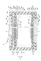
次に、蓄電モジュール4の構成について詳細に説明する。図2は、図1に示された蓄電モジュール4の内部構成を示す概略断面図である。図2に示されるように、蓄電モジュール4は、複数のバイポーラ電極14を積層してなる電極積層体(積層体)11を有し、この電極積層体11の外縁に樹脂製の封止体12を設けて構成されている。電極積層体11は、セパレータ13、セパレータ13を介して、積層方向D(第1方向)に沿って積層された複数の電極(複数のバイポーラ電極14、単一の負極終端電極18、及び、単一の正極終端電極19)を含む。ここでは、電極積層体11の積層方向Dはモジュール積層体2の積層方向と一致している。電極積層体11は、積層方向Dに延びる側面11aを有している。側面11aは、一例として、後述する電極板15の端面(第1面15aと第2面15bとを接続する面)の集合として構成される。   Next, the configuration of the power storage module 4 will be described in detail. FIG. 2 is a schematic cross-sectional view showing the internal configuration of the power storage module 4 shown in FIG. As shown in FIG. 2, the power storage module 4 has an electrode laminated body (laminated body) 11 formed by laminating a plurality of bipolar electrodes 14, and a resin sealing body 12 on the outer edge of the electrode laminated body 11. Is provided. The electrode stack 11 includes a separator 13 and a plurality of electrodes (a plurality of bipolar electrodes 14, a single negative electrode termination electrode 18, and a single electrode) stacked in the stacking direction D (first direction) via the separator 13. One positive terminal electrode 19). Here, the stacking direction D of the electrode stack 11 coincides with the stacking direction of the module stack 2. The electrode stack 11 has a side surface 11a extending in the stacking direction D. As an example, the side surface 11a is configured as a set of end surfaces (surfaces connecting the first surface 15a and the second surface 15b) of an electrode plate 15 described later.

バイポーラ電極14は、電極板15、正極16及び負極17を含んでいる。正極16は、電極板15の第1面15aに設けられている。負極17は、電極板15の第1面15aに対して反対側の第2面15bに設けられている。電極板15は、例えば、ニッケル又はニッケルメッキ鋼板といった金属からなる。一例として、電極板15は、ニッケルからなる矩形の金属箔である。電極板15は、積層方向Dから見て矩形状の外縁15dを含んでいる。   The bipolar electrode 14 includes an electrode plate 15, a positive electrode 16, and a negative electrode 17. The positive electrode 16 is provided on the first surface 15 a of the electrode plate 15. The negative electrode 17 is provided on the second surface 15 b opposite to the first surface 15 a of the electrode plate 15. The electrode plate 15 is made of a metal such as nickel or a nickel-plated steel plate, for example. As an example, the electrode plate 15 is a rectangular metal foil made of nickel. The electrode plate 15 includes a rectangular outer edge 15d as viewed from the stacking direction D.

正極16は、正極活物質が電極板15に塗工されることにより形成される正極活物質層である。正極16を構成する正極活物質としては、例えば水酸化ニッケルが挙げられる。正極16は、積層方向Dから見て矩形状の外縁16dを含んでいる。負極17は、負極活物質が電極板15に塗工されることにより形成される負極活物質層である。負極17を構成する負極活物質としては、例えば水素吸蔵合金が挙げられる。負極17は、積層方向Dから見て矩形状の外縁17dを含んでいる。   The positive electrode 16 is a positive electrode active material layer formed by applying a positive electrode active material to the electrode plate 15. An example of the positive electrode active material constituting the positive electrode 16 is nickel hydroxide. The positive electrode 16 includes a rectangular outer edge 16d when viewed from the stacking direction D. The negative electrode 17 is a negative electrode active material layer formed by applying a negative electrode active material to the electrode plate 15. As a negative electrode active material which comprises the negative electrode 17, a hydrogen storage alloy is mentioned, for example. The negative electrode 17 includes a rectangular outer edge 17d when viewed from the stacking direction D.

本実施形態では、電極板15の第2面15bにおける負極17の形成領域は、電極板15の第1面15aにおける正極16の形成領域に対して大きくなっている。つまり、負極17の外縁17dは、正極16の外縁16dよりも一回り大きい。電極板15の周縁部15cは、矩形枠状をなし、正極活物質及び負極活物質が塗工されない未塗工領域となっている。つまり、電極板15の周縁部15cは、積層方向Dから見て、電極板15における正極16及び負極17が形成された領域以外の部分であって、正極16及び負極17を包囲する部分である。なお、バイポーラ電極14、負極終端電極18、及び正極終端電極19の表面は、それぞれ電極板15の周縁部15cにおける第1面15a及び第2面15bを含んでいる。   In the present embodiment, the formation region of the negative electrode 17 on the second surface 15 b of the electrode plate 15 is larger than the formation region of the positive electrode 16 on the first surface 15 a of the electrode plate 15. That is, the outer edge 17 d of the negative electrode 17 is slightly larger than the outer edge 16 d of the positive electrode 16. The peripheral edge portion 15c of the electrode plate 15 has a rectangular frame shape and is an uncoated region where the positive electrode active material and the negative electrode active material are not coated. That is, the peripheral edge portion 15 c of the electrode plate 15 is a portion surrounding the positive electrode 16 and the negative electrode 17, as viewed from the stacking direction D, except for the region where the positive electrode 16 and the negative electrode 17 are formed. . Note that the surfaces of the bipolar electrode 14, the negative electrode termination electrode 18, and the positive electrode termination electrode 19 include a first surface 15 a and a second surface 15 b in the peripheral portion 15 c of the electrode plate 15, respectively.

電極積層体11において、一のバイポーラ電極14の正極16は、セパレータ13を挟んで積層方向Dに隣り合う別のバイポーラ電極14の負極17と対向している。電極積層体11において、一のバイポーラ電極14の負極17は、セパレータ13を挟んで積層方向Dに隣り合うさらに別のバイポーラ電極14の正極16と対向している。   In the electrode stack 11, the positive electrode 16 of one bipolar electrode 14 faces the negative electrode 17 of another bipolar electrode 14 adjacent in the stacking direction D across the separator 13. In the electrode stack 11, the negative electrode 17 of one bipolar electrode 14 faces the positive electrode 16 of another bipolar electrode 14 adjacent in the stacking direction D across the separator 13.

負極終端電極18は、電極板15、及び電極板15の第2面15bに設けられた負極17を含んでいる。負極終端電極18は、正極16を含んでいない。すなわち、負極終端電極18の電極板15の第1面15aには、活物質層が設けられていない(すなわち、負極終端電極18の第1面15aの全体が露出している)。負極終端電極18は、第2面15bが電極積層体11の積層方向Dの内側(積層方向Dについての中心側)に向くように、積層方向Dの一端に配置されている。負極終端電極18の負極17は、セパレータ13を介して、積層方向Dの一端のバイポーラ電極14の正極16と対向している。   The negative electrode termination electrode 18 includes an electrode plate 15 and a negative electrode 17 provided on the second surface 15 b of the electrode plate 15. The negative electrode termination electrode 18 does not include the positive electrode 16. That is, the active material layer is not provided on the first surface 15a of the electrode plate 15 of the negative electrode termination electrode 18 (that is, the entire first surface 15a of the negative electrode termination electrode 18 is exposed). The negative electrode termination electrode 18 is disposed at one end in the stacking direction D so that the second surface 15 b faces the inner side of the electrode stack 11 in the stacking direction D (center side in the stacking direction D). The negative electrode 17 of the negative electrode termination electrode 18 is opposed to the positive electrode 16 of the bipolar electrode 14 at one end in the stacking direction D via the separator 13.

正極終端電極19は、電極板15、及び電極板15の第1面15aに設けられた正極16を含んでいる。正極終端電極19は、負極17を含んでいない。すなわち、正極終端電極19の電極板15の第2面15bには、活物質層が設けられていない(すなわち、正極終端電極19の第2面15bの全体が露出している)。正極終端電極19は、第1面15aが電極積層体11の積層方向Dの内側に向くように、積層方向Dの他端に配置されている。正極終端電極19の正極16は、セパレータ13を介して、積層方向Dの他端のバイポーラ電極14の負極17と対向している。   The positive electrode termination electrode 19 includes an electrode plate 15 and a positive electrode 16 provided on the first surface 15 a of the electrode plate 15. The positive electrode termination electrode 19 does not include the negative electrode 17. That is, the active material layer is not provided on the second surface 15b of the electrode plate 15 of the positive electrode termination electrode 19 (that is, the entire second surface 15b of the positive electrode termination electrode 19 is exposed). The positive electrode termination electrode 19 is disposed at the other end in the stacking direction D so that the first surface 15 a faces the inside of the stacking direction D of the electrode stack 11. The positive electrode 16 of the positive electrode termination electrode 19 faces the negative electrode 17 of the bipolar electrode 14 at the other end in the stacking direction D via the separator 13.

負極終端電極18の電極板15の第1面15aには、導電板5が接触している。また、正極終端電極19の電極板15の第2面15bには、隣接する蓄電モジュール4の導電板5が接触している。拘束部材3からの拘束荷重は、導電板5を介して負極終端電極18及び正極終端電極19から電極積層体11に付加される。すなわち、導電板5は、積層方向Dに沿って電極積層体11に拘束荷重を付加する拘束部材でもある。   The conductive plate 5 is in contact with the first surface 15 a of the electrode plate 15 of the negative electrode termination electrode 18. The conductive plate 5 of the adjacent power storage module 4 is in contact with the second surface 15 b of the electrode plate 15 of the positive electrode termination electrode 19. The restraining load from the restraining member 3 is applied to the electrode laminate 11 from the negative terminal electrode 18 and the positive terminal electrode 19 via the conductive plate 5. That is, the conductive plate 5 is also a restraining member that applies a restraining load to the electrode laminate 11 along the stacking direction D.

セパレータ13は、例えばシート状に形成されている。セパレータ13としては、ポリエチレン(PE)、ポリプロピレン(PP)等のポリオレフィン系樹脂からなる多孔質フィルム、ポリプロピレン、メチルセルロース等からなる織布又は不織布等が例示される。セパレータ13は、フッ化ビニリデン樹脂化合物で補強されたものであってもよい。なお、セパレータ13は、シート状に限られず、袋状のものを用いてもよい。   The separator 13 is formed in a sheet shape, for example. Examples of the separator 13 include a porous film made of a polyolefin resin such as polyethylene (PE) and polypropylene (PP), and a woven or non-woven fabric made of polypropylene, methylcellulose, or the like. The separator 13 may be reinforced with a vinylidene fluoride resin compound. The separator 13 is not limited to a sheet shape, and may be a bag shape.

封止体12は、例えば絶縁性の樹脂によって形成されている。封止体12は、周縁部15cを包囲するように電極積層体11の側面11aに沿って設けられている。封止体12は、周縁部15cを保持している。バイポーラ電極14には、中間樹脂部23が設けられている。中間樹脂部23は、バイポーラ電極14の外縁に沿って設けられ、バイポーラ電極14の全周に亘って設けられている。中間樹脂部23は、電極板15の外縁に接合して設けられている。この中間樹脂部23の端部は、封止体12に接合されている。つまり、バイポーラ電極14は、中間樹脂部23を介して封止体12に接合され、封止体12に支持されている。中間樹脂部23は、第1中間樹脂部231と第2中間樹脂部232とを有している。第1中間樹脂部231と第2中間樹脂部232の詳細については、後述する。   The sealing body 12 is made of, for example, an insulating resin. The sealing body 12 is provided along the side surface 11a of the electrode laminate 11 so as to surround the peripheral edge portion 15c. The sealing body 12 holds the peripheral edge portion 15c. The bipolar electrode 14 is provided with an intermediate resin portion 23. The intermediate resin portion 23 is provided along the outer edge of the bipolar electrode 14 and is provided over the entire circumference of the bipolar electrode 14. The intermediate resin portion 23 is provided to be joined to the outer edge of the electrode plate 15. An end portion of the intermediate resin portion 23 is joined to the sealing body 12. That is, the bipolar electrode 14 is joined to the sealing body 12 via the intermediate resin portion 23 and supported by the sealing body 12. The intermediate resin part 23 has a first intermediate resin part 231 and a second intermediate resin part 232. Details of the first intermediate resin portion 231 and the second intermediate resin portion 232 will be described later.

図3は、積層方向Dから見た場合における中間樹脂部23が溶着されたバイポーラ電極14を示す図である。図4は、積層方向Dから見た場合における負極終端樹脂部24が溶着された負極終端電極18を示す図である。図5は、積層方向Dから見た場合におけるバイポーラ電極14及び負極終端電極18を示す図である。なお、図5に示されるバイポーラ電極14及び負極終端電極18は、それぞれ中間樹脂部23及び負極終端樹脂部24が溶着されており、互いに積層されている。   FIG. 3 is a diagram showing the bipolar electrode 14 to which the intermediate resin portion 23 is welded when viewed from the stacking direction D. FIG. FIG. 4 is a view showing the negative electrode termination electrode 18 to which the negative electrode termination resin portion 24 is welded when viewed from the stacking direction D. FIG. 5 is a diagram showing the bipolar electrode 14 and the negative electrode termination electrode 18 when viewed from the stacking direction D. FIG. The bipolar electrode 14 and the negative electrode termination electrode 18 shown in FIG. 5 are laminated with each other, with the intermediate resin portion 23 and the negative electrode termination resin portion 24 being welded to each other.

図2〜図5において、中間樹脂部23は所定の厚さ(積層方向Dの長さ)を有するフィルムである。中間樹脂部23は、積層方向Dから見て、矩形枠状をなし、上述したようにバイポーラ電極14の周縁部15cの全周にわたって連続的に設けられている。中間樹脂部23は、積層方向Dから見て矩形状の内縁23c及び矩形状の外縁23dを含んでいる。中間樹脂部23は、バイポーラ電極14の少なくとも周縁部15cにおいてバイポーラ電極14の表面に溶着されている。具体的には、中間樹脂部23は、バイポーラ電極14の第1面15aに溶着されて気密(液密)にバイポーラ電極14に接合されている。   2 to 5, the intermediate resin portion 23 is a film having a predetermined thickness (length in the stacking direction D). The intermediate resin portion 23 has a rectangular frame shape when viewed from the stacking direction D, and is continuously provided over the entire circumference of the peripheral edge portion 15c of the bipolar electrode 14 as described above. The intermediate resin portion 23 includes a rectangular inner edge 23 c and a rectangular outer edge 23 d as viewed from the stacking direction D. The intermediate resin portion 23 is welded to the surface of the bipolar electrode 14 at least at the peripheral edge portion 15 c of the bipolar electrode 14. Specifically, the intermediate resin portion 23 is welded to the first surface 15a of the bipolar electrode 14 and joined to the bipolar electrode 14 in an airtight (liquid tight) manner.

中間樹脂部23は、第1中間樹脂部231と第2中間樹脂部232とを有している。第1中間樹脂部231及び第2中間樹脂部232は、積層方向Dに沿って互いに積層されている。第1中間樹脂部231及び第2中間樹脂部232のそれぞれは、積層方向Dから見て、矩形枠状をなし、矩形状の内縁及び外縁を含んでいる。積層方向Dから見て、第1中間樹脂部231の外縁及び第2中間樹脂部232の外縁は、互いに一致しており中間樹脂部23の外縁23dを構成している。   The intermediate resin part 23 has a first intermediate resin part 231 and a second intermediate resin part 232. The first intermediate resin portion 231 and the second intermediate resin portion 232 are laminated together along the lamination direction D. Each of the first intermediate resin portion 231 and the second intermediate resin portion 232 has a rectangular frame shape when viewed in the stacking direction D, and includes a rectangular inner edge and an outer edge. When viewed from the stacking direction D, the outer edge of the first intermediate resin portion 231 and the outer edge of the second intermediate resin portion 232 coincide with each other to form the outer edge 23 d of the intermediate resin portion 23.

積層方向Dから見て、第2中間樹脂部232の内縁は、第1中間樹脂部231の内縁よりも大きい矩形状である。これにより、中間樹脂部23には、段差部23eが形成されている。段差部23e上には、セパレータ13の縁部が載置されている。第1中間樹脂部231の内縁は、中間樹脂部23の内縁23cを構成している。第1中間樹脂部231は、バイポーラ電極14の第1面15aに溶着されて電極板15に接合されている。第2中間樹脂部232は、第1中間樹脂部231上に溶着されて第1中間樹脂部231に接合されている。   When viewed from the stacking direction D, the inner edge of the second intermediate resin portion 232 has a rectangular shape that is larger than the inner edge of the first intermediate resin portion 231. Thereby, a stepped portion 23 e is formed in the intermediate resin portion 23. The edge of the separator 13 is placed on the step portion 23e. The inner edge of the first intermediate resin portion 231 constitutes the inner edge 23 c of the intermediate resin portion 23. The first intermediate resin portion 231 is welded to the first surface 15 a of the bipolar electrode 14 and joined to the electrode plate 15. The second intermediate resin portion 232 is welded onto the first intermediate resin portion 231 and joined to the first intermediate resin portion 231.

負極終端樹脂部24は所定の厚さ(積層方向Dの長さ)を有するフィルムである。負極終端樹脂部24は、積層方向Dから見て、矩形枠状をなし、負極終端電極18の周縁部15cの全周にわたって連続的に設けられている。負極終端樹脂部24は、積層方向Dから見て矩形状の内縁24c及び矩形状の外縁24dを含んでいる。負極終端樹脂部24は、負極終端電極18の少なくとも周縁部15cにおいて負極終端電極18の表面に溶着されている。具体的には、負極終端樹脂部24は、負極終端電極18の第1面15aに溶着されて気密(液密)に負極終端電極18に接合されている。   The negative electrode termination resin portion 24 is a film having a predetermined thickness (length in the stacking direction D). The negative electrode termination resin portion 24 has a rectangular frame shape when viewed from the stacking direction D, and is continuously provided over the entire circumference of the peripheral edge portion 15 c of the negative electrode termination electrode 18. The negative terminal resin portion 24 includes a rectangular inner edge 24 c and a rectangular outer edge 24 d when viewed from the stacking direction D. The negative electrode termination resin portion 24 is welded to the surface of the negative electrode termination electrode 18 at least at the peripheral edge portion 15 c of the negative electrode termination electrode 18. Specifically, the negative electrode termination resin portion 24 is welded to the first surface 15a of the negative electrode termination electrode 18 and joined to the negative electrode termination electrode 18 in an airtight (liquid tight) manner.

正極終端樹脂部25、26は所定の厚さ(積層方向Dの長さ)を有するフィルムである。正極終端樹脂部25、26は、積層方向Dから見て、矩形枠状をなし、正極終端電極19の周縁部15cの全周にわたって連続的に設けられている。正極終端樹脂部25は、積層方向Dから見て矩形状の内縁25c及び矩形状の外縁25dを含んでいる。正極終端樹脂部25は、正極終端電極19の少なくとも周縁部15cにおいて正極終端電極19の表面に溶着されている。具体的には、正極終端樹脂部25は、正極終端電極19の第1面15aに溶着されて気密(液密)に正極終端電極19に接合されている。   The positive electrode termination resin portions 25 and 26 are films having a predetermined thickness (length in the stacking direction D). The positive electrode termination resin portions 25 and 26 have a rectangular frame shape when viewed from the stacking direction D, and are continuously provided over the entire circumference of the peripheral edge portion 15 c of the positive electrode termination electrode 19. The positive electrode termination resin portion 25 includes a rectangular inner edge 25 c and a rectangular outer edge 25 d when viewed from the stacking direction D. The positive electrode termination resin portion 25 is welded to the surface of the positive electrode termination electrode 19 at least at the peripheral edge portion 15 c of the positive electrode termination electrode 19. Specifically, the positive electrode termination resin portion 25 is welded to the first surface 15 a of the positive electrode termination electrode 19 and joined to the positive electrode termination electrode 19 in an airtight (liquid tight) manner.

正極終端樹脂部25は、第1部分251と第2部分252とを有している。第1部分251及び第2部分252は、積層方向Dに沿って互いに積層されている。第1部分251及び第2部分252のそれぞれは、積層方向Dから見て、それぞれ矩形枠状をなし、矩形状の内縁及び外縁を含んでいる。積層方向Dから見て、第1部分251の外縁及び第2部分252の外縁は、互いに一致しており正極終端樹脂部25の外縁25dを構成している。積層方向Dから見て、第2部分252の内縁は、第1部分251の内縁よりも一回り大きい矩形状である。これにより、正極終端樹脂部25には、段差部25eが形成されている。段差部25e上には、セパレータ13の縁部が載置されている。第1部分251の内縁は、正極終端樹脂部25の内縁25cを構成している。第1部分251は、正極終端電極19の第1面15aに溶着されて電極板15に接合されている。第2部分252は、第1部分251上に溶着されて第1部分251に接合されている。   The positive electrode termination resin portion 25 has a first portion 251 and a second portion 252. The first portion 251 and the second portion 252 are stacked on each other along the stacking direction D. Each of the first portion 251 and the second portion 252 has a rectangular frame shape when viewed from the stacking direction D, and includes a rectangular inner edge and an outer edge. When viewed from the stacking direction D, the outer edge of the first portion 251 and the outer edge of the second portion 252 coincide with each other and constitute an outer edge 25 d of the positive electrode termination resin portion 25. When viewed from the stacking direction D, the inner edge of the second portion 252 has a rectangular shape that is slightly larger than the inner edge of the first portion 251. Thereby, a step portion 25 e is formed in the positive electrode termination resin portion 25. The edge of the separator 13 is placed on the step portion 25e. An inner edge of the first portion 251 constitutes an inner edge 25 c of the positive electrode termination resin portion 25. The first portion 251 is welded to the first surface 15 a of the positive electrode termination electrode 19 and joined to the electrode plate 15. The second portion 252 is welded onto the first portion 251 and joined to the first portion 251.

正極終端樹脂部26は、積層方向Dから見て矩形状の内縁26c及び矩形状の外縁26dを含んでいる。正極終端樹脂部26は、正極終端電極19の少なくとも周縁部15cにおいて正極終端電極19の表面に溶着されている。具体的には、正極終端樹脂部26は、正極終端電極19の第2面15bに溶着されて気密(液密)に正極終端電極19に接合されている。   The positive electrode termination resin portion 26 includes a rectangular inner edge 26 c and a rectangular outer edge 26 d when viewed from the stacking direction D. The positive electrode termination resin portion 26 is welded to the surface of the positive electrode termination electrode 19 at least at the peripheral edge portion 15 c of the positive electrode termination electrode 19. Specifically, the positive electrode termination resin portion 26 is welded to the second surface 15 b of the positive electrode termination electrode 19 and joined to the positive electrode termination electrode 19 in an airtight (liquid tight) manner.

中間樹脂部23、負極終端樹脂部24、及び正極終端樹脂部25のそれぞれは、例えば超音波又は熱によって第1面15aに溶着されている。電極板15の端面は、中間樹脂部23、負極終端樹脂部24、及び正極終端樹脂部25によって覆われておらず露出している。中間樹脂部23、負極終端樹脂部24、及び正極終端樹脂部25のそれぞれの内側端部は、積層方向Dに互いに隣り合う電極板15の周縁部15c同士の間に位置しており、外側端部は、積層方向Dからみて電極板15から外側に張り出している。中間樹脂部23、負極終端樹脂部24、及び正極終端樹脂部25のそれぞれは、当該外側端部において第2樹脂部22に埋設されている。積層方向Dに沿って互いに隣り合う第1樹脂部21同士は、互いに離間している。   Each of the intermediate resin portion 23, the negative electrode termination resin portion 24, and the positive electrode termination resin portion 25 is welded to the first surface 15a by, for example, ultrasonic waves or heat. The end surface of the electrode plate 15 is not covered with the intermediate resin portion 23, the negative electrode termination resin portion 24, and the positive electrode termination resin portion 25 and is exposed. The inner end portions of the intermediate resin portion 23, the negative electrode termination resin portion 24, and the positive electrode termination resin portion 25 are located between the peripheral portions 15 c of the electrode plates 15 adjacent to each other in the stacking direction D, and the outer end portions The portion projects outward from the electrode plate 15 as viewed from the stacking direction D. Each of the intermediate resin portion 23, the negative electrode termination resin portion 24, and the positive electrode termination resin portion 25 is embedded in the second resin portion 22 at the outer end portion. The first resin portions 21 adjacent to each other along the stacking direction D are separated from each other.

封止体12は、積層方向Dに沿って互いに隣接するバイポーラ電極14の間、積層方向Dに沿って互いに隣接する負極終端電極18とバイポーラ電極14との間、及び、積層方向Dに沿って互いに隣接する正極終端電極19とバイポーラ電極14との間をそれぞれ封止している。これにより、バイポーラ電極14の間、負極終端電極18とバイポーラ電極14との間、及び、正極終端電極19とバイポーラ電極14との間には、それぞれ気密(液密)に仕切られた内部空間Vが形成されている。この内部空間Vには、例えば水酸化カリウム水溶液等のアルカリ水溶液からなる電解液(不図示)が収容されている。すなわち、第1樹脂部21は、積層方向Dに沿って隣接する電極の間に電解液が収容される内部空間Vを形成すると共に、内部空間Vを封止するためのものである。電解液は、セパレータ13、正極16及び負極17内に含浸されている。   The sealing body 12 is formed between the bipolar electrodes 14 adjacent to each other along the stacking direction D, between the negative electrode termination electrode 18 and the bipolar electrode 14 adjacent to each other along the stacking direction D, and along the stacking direction D. The space between the positive electrode termination electrode 19 and the bipolar electrode 14 adjacent to each other is sealed. As a result, the internal space V partitioned between the bipolar electrodes 14, between the negative electrode termination electrode 18 and the bipolar electrode 14, and between the positive electrode termination electrode 19 and the bipolar electrode 14 is hermetically (liquid-tight) partitioned. Is formed. In the internal space V, an electrolytic solution (not shown) made of an alkaline aqueous solution such as an aqueous potassium hydroxide solution is accommodated. That is, the first resin portion 21 is for forming the internal space V in which the electrolytic solution is accommodated between the electrodes adjacent along the stacking direction D and sealing the internal space V. The electrolytic solution is impregnated in the separator 13, the positive electrode 16, and the negative electrode 17.

封止体12は、例えば、絶縁性の樹脂であって、ポリプロピレン(PP)、ポリフェニレンサルファイド(PPS)、又は変性ポリフェニレンエーテル(変性PPE)等から構成され得る。   The sealing body 12 is, for example, an insulating resin and can be made of polypropylene (PP), polyphenylene sulfide (PPS), modified polyphenylene ether (modified PPE), or the like.

続いて、各部の相対的な関係について詳細に説明する。なお、内側とは、積層方向Dから見て、蓄電モジュール4の中心の側をいう。外側とは、積層方向Dから見て、蓄電モジュール4の中心から遠ざかる側をいう。バイポーラ電極14において、負極17は、電極板15よりも一回り小さい。つまり、負極17の外縁17dは、電極板15の外縁15dよりも内側に位置している。正極16は、負極17よりも一回り小さい。つまり、正極16の外縁16dは、負極17の外縁17dよりも内側に位置している。中間樹脂部23の外縁23dは、電極板15の外縁15dの外側に位置している。中間樹脂部23の内縁23cは、電極板15の外縁15dと負極17の外縁17dとの間に位置している。   Next, the relative relationship between the units will be described in detail. The inner side refers to the center side of the power storage module 4 when viewed from the stacking direction D. The outside refers to a side away from the center of the power storage module 4 when viewed from the stacking direction D. In the bipolar electrode 14, the negative electrode 17 is slightly smaller than the electrode plate 15. That is, the outer edge 17 d of the negative electrode 17 is located inside the outer edge 15 d of the electrode plate 15. The positive electrode 16 is slightly smaller than the negative electrode 17. That is, the outer edge 16 d of the positive electrode 16 is located inside the outer edge 17 d of the negative electrode 17. The outer edge 23 d of the intermediate resin portion 23 is located outside the outer edge 15 d of the electrode plate 15. The inner edge 23 c of the intermediate resin portion 23 is located between the outer edge 15 d of the electrode plate 15 and the outer edge 17 d of the negative electrode 17.

中間樹脂部23は、第1エリア15e(図3においてハッチングが施された領域)においてバイポーラ電極14の表面(ここでは、バイポーラ電極14の第1面15a)に溶着されている。換言すれば、第1エリア15eは、バイポーラ電極14の第1面15aにおける中間樹脂部23が溶着されたエリアであって、電極板15の外縁15d及び中間樹脂部23の内縁23cにより矩形枠状に規定されたエリアである。   The intermediate resin portion 23 is welded to the surface of the bipolar electrode 14 (here, the first surface 15a of the bipolar electrode 14) in the first area 15e (the hatched region in FIG. 3). In other words, the first area 15 e is an area where the intermediate resin portion 23 is welded on the first surface 15 a of the bipolar electrode 14, and has a rectangular frame shape by the outer edge 15 d of the electrode plate 15 and the inner edge 23 c of the intermediate resin portion 23. This is an area defined in

負極終端電極18において、負極17は、電極板15よりも一回り小さい。つまり、負極17の外縁17dは、電極板15の外縁15dよりも内側に位置している。正極16は、負極17よりも一回り小さい。つまり、正極16の外縁16dは、負極17の外縁17dよりも内側に位置している。負極終端樹脂部24の外縁24dは、電極板15の外縁15dの外側に位置している。負極終端樹脂部24の内縁24cは、正極16の外縁16dよりも内側に位置している。つまり、負極終端樹脂部24は、正極16に重なるように延在している。   In the negative electrode termination electrode 18, the negative electrode 17 is slightly smaller than the electrode plate 15. That is, the outer edge 17 d of the negative electrode 17 is located inside the outer edge 15 d of the electrode plate 15. The positive electrode 16 is slightly smaller than the negative electrode 17. That is, the outer edge 16 d of the positive electrode 16 is located inside the outer edge 17 d of the negative electrode 17. The outer edge 24 d of the negative electrode termination resin portion 24 is located outside the outer edge 15 d of the electrode plate 15. The inner edge 24 c of the negative electrode termination resin portion 24 is located inside the outer edge 16 d of the positive electrode 16. That is, the negative electrode termination resin portion 24 extends so as to overlap the positive electrode 16.

負極終端樹脂部24は、第2エリア15f(図4においてハッチングが施された領域)において負極終端電極18の表面(ここでは、負極終端電極18の第1面15a)に溶着されている。換言すれば、第2エリア15fは、負極終端電極18の第1面15aにおける負極終端樹脂部24が溶着されたエリアであって、電極板15の外縁15d及び負極終端樹脂部24の内縁24cにより矩形枠状に規定されたエリアである。   The negative electrode termination resin portion 24 is welded to the surface of the negative electrode termination electrode 18 (here, the first surface 15a of the negative electrode termination electrode 18) in the second area 15f (the hatched region in FIG. 4). In other words, the second area 15 f is an area where the negative electrode termination resin portion 24 is welded on the first surface 15 a of the negative electrode termination electrode 18, and is formed by the outer edge 15 d of the electrode plate 15 and the inner edge 24 c of the negative electrode termination resin portion 24. This is an area defined as a rectangular frame.

バイポーラ電極14及び負極終端電極18の電極板15の外縁15dは、互いに一致している。バイポーラ電極14及び負極終端電極18のそれぞれの負極17の外縁17dは、互いに一致している。中間樹脂部23の外縁23d及び負極終端樹脂部24の外縁24dは、互いに一致している。負極終端樹脂部24の内縁24cは、中間樹脂部23の内縁23cよりも内側に位置している。つまり、第2エリア15fは、第1エリア15eよりも大きい。すなわち、積層方向Dに沿った全ての断面において、第2エリア15fの長さ(矩形枠状の幅)は、第1エリア15eの長さ(矩形枠状の幅)よりも大きい(図2参照)。つまり、積層方向Dから見て電極積層体11の全周に亘って、負極終端電極18の電極板15の外縁15dと負極終端樹脂部24の内縁24cとの距離は、バイポーラ電極14の電極板15の外縁15dと中間樹脂部23の内縁23cとの距離よりも大きい。   The outer edges 15d of the electrode plate 15 of the bipolar electrode 14 and the negative electrode termination electrode 18 coincide with each other. The outer edges 17d of the negative electrodes 17 of the bipolar electrode 14 and the negative electrode termination electrode 18 are coincident with each other. The outer edge 23d of the intermediate resin portion 23 and the outer edge 24d of the negative electrode termination resin portion 24 are coincident with each other. The inner edge 24 c of the negative electrode termination resin portion 24 is located inside the inner edge 23 c of the intermediate resin portion 23. That is, the second area 15f is larger than the first area 15e. That is, in all cross sections along the stacking direction D, the length of the second area 15f (rectangular frame width) is larger than the length of the first area 15e (rectangular frame width) (see FIG. 2). ). That is, the distance between the outer edge 15d of the electrode plate 15 of the negative electrode termination electrode 18 and the inner edge 24c of the negative electrode termination resin portion 24 over the entire circumference of the electrode laminate 11 when viewed from the lamination direction D is the electrode plate of the bipolar electrode 14 The distance between the 15 outer edges 15 d and the inner edge 23 c of the intermediate resin portion 23 is larger.

正極終端樹脂部25は、第1エリア15gにおいて正極終端電極19の表面(ここでは、正極終端電極19の第1面15a)に溶着されている。換言すれば、第1エリア15gは、正極終端電極19の第1面15aにおける正極終端樹脂部25が溶着されたエリアであって、電極板15の外縁15d及び正極終端樹脂部25の内縁25cにより矩形枠状に規定されたエリアである。正極終端樹脂部26は、正極終端電極19の表面(ここでは、正極終端電極19の第2面15b)に溶着されて正極終端電極19に接合されている。   The positive electrode termination resin portion 25 is welded to the surface of the positive electrode termination electrode 19 (here, the first surface 15a of the positive electrode termination electrode 19) in the first area 15g. In other words, the first area 15g is an area where the positive electrode termination resin portion 25 on the first surface 15a of the positive electrode termination electrode 19 is welded, and is formed by the outer edge 15d of the electrode plate 15 and the inner edge 25c of the positive electrode termination resin portion 25. This is an area defined as a rectangular frame. The positive electrode termination resin portion 26 is welded to the surface of the positive electrode termination electrode 19 (here, the second surface 15 b of the positive electrode termination electrode 19) and joined to the positive electrode termination electrode 19.

次に、本実施形態に係る蓄電モジュール4の製造方法について説明する。   Next, a method for manufacturing the power storage module 4 according to this embodiment will be described.

図6は、蓄電モジュール4の製造工程を示すフローチャートである。図6に示すように、蓄電モジュール4の製造として、まず、電極積層体11の作製が行われる(S10)。電極積層体11の作製は、複数のバイポーラ電極14を重ね合わせて積層させて行われる。バイポーラ電極14には、積層される前に予め中間樹脂部23などが取り付けられている。なお、電極積層体11には、バイポーラ電極14のほか、負極終端電極18及び正極終端電極19も積層される。   FIG. 6 is a flowchart showing a manufacturing process of the power storage module 4. As shown in FIG. 6, as the storage module 4, first, the electrode laminate 11 is manufactured (S <b> 10). The electrode stack 11 is manufactured by stacking a plurality of bipolar electrodes 14 in a stacked manner. The bipolar electrode 14 is previously attached with an intermediate resin portion 23 and the like before being laminated. In addition to the bipolar electrode 14, a negative electrode termination electrode 18 and a positive electrode termination electrode 19 are also laminated on the electrode laminate 11.

次いで、封止体12の成形が行われる(S12)。この成形工程は、電極積層体11の外縁に封止体12を樹脂成形する工程である。例えば、電極積層体11をインサート部材として射出成形が行われ、電極積層体11の周囲に封止体12が成形される。成形工程の詳細については、後述する。   Next, the sealing body 12 is molded (S12). This forming step is a step of resin-molding the sealing body 12 on the outer edge of the electrode laminate 11. For example, injection molding is performed using the electrode laminate 11 as an insert member, and the sealing body 12 is molded around the electrode laminate 11. Details of the molding process will be described later.

図7は、蓄電モジュール4の製造における封止体12の樹脂成形の工程概要図である。蓄電モジュール4は、電極積層体11の外縁に封止体12を樹脂成形することにより製造される。図7の(a)は、電極積層体11の配置工程を示した図である。すなわち、電極積層体11は、インサート部材として、金型91内に配置される。電極積層体11は、複数のバイポーラ電極14を積層させて構成され、樹脂成形の前に予め製造される。金型91は固定側の金型であり、この金型91の所定の位置に電極積層体11が配置される。   FIG. 7 is a process schematic diagram of resin molding of the sealing body 12 in the manufacture of the power storage module 4. The power storage module 4 is manufactured by resin-molding the sealing body 12 on the outer edge of the electrode laminate 11. FIG. 7A is a diagram showing an arrangement process of the electrode laminate 11. That is, the electrode laminated body 11 is arrange | positioned in the metal mold | die 91 as an insert member. The electrode laminate 11 is configured by laminating a plurality of bipolar electrodes 14 and is manufactured in advance before resin molding. The mold 91 is a fixed mold, and the electrode stack 11 is disposed at a predetermined position of the mold 91.

図7の(b)、(c)は、電極積層体11の外縁に封止体12を樹脂成形する成形工程の説明図である。図7の(b)に示すように、型締めが行われ、金型91に対し金型92が接合される。金型92は、可動側の金型であり、金型91に対し接近及び離間可能となっている。金型91と金型92が接合された内部には、空洞部(キャビティ)93が形成される。空洞部93は、封止体12の成形領域である。すなわち、この空洞部93に樹脂Pが流し込まれることにより、封止体12が成形される。空洞部93へは、封止体12の角部93aの位置から樹脂Pが注入されて樹脂成形が行われる。空洞部93への樹脂Pの注入は、ゲート94を通じて行われる。   7B and 7C are explanatory views of a molding process for resin molding the sealing body 12 on the outer edge of the electrode laminate 11. As shown in FIG. 7B, mold clamping is performed, and the mold 92 is joined to the mold 91. The mold 92 is a movable mold, and can be moved toward and away from the mold 91. A cavity portion (cavity) 93 is formed in the inside where the mold 91 and the mold 92 are joined. The cavity 93 is a molding region of the sealing body 12. That is, the sealing body 12 is formed by pouring the resin P into the hollow portion 93. The resin P is injected into the cavity 93 from the position of the corner 93a of the sealing body 12, and resin molding is performed. The resin P is injected into the cavity 93 through the gate 94.

図8は、ゲート94の位置の説明図であり、金型91の断面であって電極積層体11の積層方向と直交する方向(図7のVIII-VIII)の断面を示している。図8に示すように、金型91には、電極積層体11の外縁の全周にわたり所定の幅で空洞部93が形成されている。空洞部93の複数の位置にゲート94が形成されている。ゲート94は、空洞部93への樹脂Pの注入口である。ゲート94は、図8に図示されていない金型92に複数形成されている。複数のゲート94のうち一部は、空洞部93(封止体12の成形領域)の角部93aに形成されている。図8では、矩形枠状に形成される空洞部93の四つの角部93aに一つずつゲート94が形成されている。また、空洞部93の長辺には二つのゲート94が形成され、空洞部93の短辺には一つのゲート94が形成されている。なお、ゲート94が角部93aにのみ形成される場合、又は、長辺及び短辺のゲート94が上述のものと異なる数で形成される場合もある。   FIG. 8 is an explanatory diagram of the position of the gate 94 and shows a cross section of the die 91 in a direction (VIII-VIII in FIG. 7) perpendicular to the stacking direction of the electrode stack 11. As shown in FIG. 8, a cavity 93 is formed in the mold 91 with a predetermined width over the entire circumference of the outer edge of the electrode stack 11. Gates 94 are formed at a plurality of positions in the cavity 93. The gate 94 is an inlet for the resin P into the cavity 93. A plurality of gates 94 are formed in a mold 92 not shown in FIG. A part of the plurality of gates 94 is formed in the corner 93a of the cavity 93 (molded region of the sealing body 12). In FIG. 8, one gate 94 is formed at each of four corners 93a of the cavity 93 formed in a rectangular frame shape. Two gates 94 are formed on the long side of the cavity portion 93, and one gate 94 is formed on the short side of the cavity portion 93. In some cases, the gates 94 are formed only at the corners 93a, or the long side and short side gates 94 are formed in a number different from that described above.

また、封止体12の樹脂成形を行う際、各々のゲート94から注入される樹脂Pの注入量を同一としてもよい。この場合、成形工程においてゲート94の各々から同一の量の樹脂Pが注入されて封止体12が成形されることにより、金型91、92内で樹脂Pを円滑に流動させることができる。つまり、封止体12の樹脂成形を行うにあたり、各ゲート94が受け持つ樹脂Pの量を同一とすることにより、各ゲート94における樹脂Pの注入がほぼ同時に完了し、樹脂Pの流れが乱れずに円滑なものとなる。これにより、封止体12の成形不良の発生が抑制され、蓄電モジュール4の製造が適切に行える。なお、ここでいう同一の注入量とは、ほぼ同一の注入量も含む。樹脂Pを円滑に流動できる注入量であれば、同一の注入量でなくてもよく、ほぼ同一の注入量であってもよい。   Further, when the resin molding of the sealing body 12 is performed, the injection amount of the resin P injected from each gate 94 may be the same. In this case, in the molding process, the same amount of resin P is injected from each of the gates 94 and the sealing body 12 is molded, so that the resin P can flow smoothly in the molds 91 and 92. In other words, when the resin molding of the sealing body 12 is performed, by making the amount of the resin P that each gate 94 is responsible for, the injection of the resin P in each gate 94 is completed almost simultaneously, and the flow of the resin P is not disturbed. It will be smooth. Thereby, generation | occurrence | production of the shaping | molding defect of the sealing body 12 is suppressed, and manufacture of the electrical storage module 4 can be performed appropriately. Note that the same injection amount here includes substantially the same injection amount. As long as the injection amount is such that the resin P can flow smoothly, the injection amount may not be the same and may be approximately the same.

また、封止体12の樹脂成形を行う際、隣り合うゲート94とゲート94の間の距離dを同一としてもよい。図8に示すように、ゲート94とゲート94の間の距離dを同一とし、そのゲート94の位置から樹脂Pを注入して成形を行うことにより、ゲート94から注入される樹脂Pが円滑に流動して成形が行える。例えば、図9に示すように、樹脂Pが予め設定された方向へ流れ、樹脂Pを流れの乱れが抑制され、安定して樹脂成形が行える。これにより、封止体12の成形不良の発生が抑制され、蓄電モジュール4の製造が適切に行える。ここでいう同一の距離とは、ほぼ同一の距離も含む。樹脂Pを円滑に流動できる距離であれば、同一の距離でなくてもよく、ほぼ同一の距離であってもよい。   Further, when the sealing body 12 is resin-molded, the distance d between the adjacent gates 94 may be the same. As shown in FIG. 8, the distance d between the gate 94 and the gate 94 is made the same, and the resin P injected from the gate 94 is smoothly formed by injecting the resin P from the position of the gate 94 and molding. It can flow and mold. For example, as shown in FIG. 9, the resin P flows in a preset direction, the flow of the resin P is prevented from being disturbed, and the resin molding can be performed stably. Thereby, generation | occurrence | production of the shaping | molding defect of the sealing body 12 is suppressed, and manufacture of the electrical storage module 4 can be performed appropriately. Here, the same distance includes almost the same distance. As long as the resin P can flow smoothly, the distance may not be the same, but may be substantially the same.

また、角部93aに形成されるゲート94の位置は、空洞部93(成形領域)の幅方向の中央位置でなく、幅方向において中央位置に対し外側の位置としてもよい。例えば、図10に示すように、電極積層体11の外縁に沿って所定の幅で矩形に形成される空洞部93において、角部93aの中央より外側の位置にゲート94が形成される。つまり、空洞部93の角部93aにおいて、内縁より外縁に近い位置にゲート94が形成される。この場合、角部93aのゲート94から空洞部93へ樹脂Pが注入されると、角部93aから二方向へ延びる成形領域へ樹脂Pが円滑に流れていくこととなる。これに対し、図11に示すように、ゲート94が角部93aの中央の位置に形成されている場合、角部93aのゲート94から空洞部93へ樹脂Pが注入されると、角部93aの外側へ流動する樹脂Pを生ずる。このため、角部93aから二方向へ延びる成形領域へ樹脂Pが円滑に流れず、樹脂Pの流れに乱れを生ずることとなり、成形不良を生ずるおそれがある。   Further, the position of the gate 94 formed in the corner portion 93a may be a position outside the center position in the width direction, not the center position in the width direction of the cavity portion 93 (molding region). For example, as shown in FIG. 10, in the cavity 93 formed in a rectangular shape with a predetermined width along the outer edge of the electrode laminate 11, a gate 94 is formed at a position outside the center of the corner 93a. That is, the gate 94 is formed at a position closer to the outer edge than the inner edge in the corner 93a of the cavity 93. In this case, when the resin P is injected from the gate 94 of the corner portion 93a into the cavity portion 93, the resin P smoothly flows from the corner portion 93a to the molding region extending in two directions. On the other hand, as shown in FIG. 11, when the gate 94 is formed at the center position of the corner 93a, when the resin P is injected from the gate 94 of the corner 93a into the cavity 93, the corner 93a. Resin P that flows outward is produced. For this reason, the resin P does not smoothly flow from the corner portion 93a to the molding region extending in two directions, and the flow of the resin P is disturbed, which may cause molding defects.

さらに、封止体12の樹脂成形を行う際、角部93aにあるゲート94とそれ以外のゲート94の樹脂Pの注入開始のタイミングを異ならせてもよい。つまり、ゲート94を開閉するゲート開閉機構を設け、ゲート94における樹脂Pの注入開始のタイミングを制御してもよい。例えば、角部93a以外にあるゲート94の樹脂Pの注入より先に角部93aにあるゲート94の樹脂Pの注入が行われる。この場合、角部93aにあるゲート94から早いタイミングで樹脂Pの注入が開始される。これにより、角部93a付近における樹脂Pの流れが乱れることが抑制され、角部93aの周辺の樹脂Pの円滑な流れが確保される。従って、角部93aにおける封止体12の成形不良の発生を抑制することができる。   Furthermore, when resin molding of the sealing body 12 is performed, the injection start timing of the resin P in the gate 94 at the corner 93a and the other gate 94 may be different. That is, a gate opening / closing mechanism that opens and closes the gate 94 may be provided to control the timing of starting the injection of the resin P in the gate 94. For example, the injection of the resin P for the gate 94 at the corner 93a is performed prior to the injection of the resin P for the gate 94 other than the corner 93a. In this case, the injection of the resin P is started at an early timing from the gate 94 at the corner 93a. Thereby, the disturbance of the flow of the resin P in the vicinity of the corner portion 93a is suppressed, and a smooth flow of the resin P around the corner portion 93a is ensured. Therefore, generation | occurrence | production of the shaping | molding defect of the sealing body 12 in the corner | angular part 93a can be suppressed.

そして、図7の(c)に示すように、空洞部93の全体に樹脂Pを充填したら、所定時間、樹脂Pに圧力を加えつつ、樹脂Pの冷却が行われる。これにより、封止体12が成形される。   Then, as shown in FIG. 7C, after filling the entire cavity 93 with the resin P, the resin P is cooled while applying pressure to the resin P for a predetermined time. Thereby, the sealing body 12 is shape | molded.

そして、型開きを行い、金型91から金型92を離間させる。その後、電極積層体11の外縁に封止体12を成形した成形品を金型91から取り出し、樹脂Pの不要部分の切り取るなどの処理を行って、蓄電モジュール4の製造が完了する。   Then, mold opening is performed to separate the mold 92 from the mold 91. Thereafter, the molded product in which the sealing body 12 is formed on the outer edge of the electrode laminate 11 is taken out from the mold 91 and unnecessary parts of the resin P are cut off, whereby the production of the power storage module 4 is completed.

以上のように、本実施形態に係る蓄電モジュール4の製造方法によれば、電極積層体11の外縁に封止体12を樹脂成形する際に、封止体12の成形領域の角部93aの位置から樹脂Pを注入して行うことにより、樹脂Pの流動方向を大きく変えることなく樹脂成形が行える。このため、封止体12の成形不良を抑制して蓄電モジュールの製造を適切に行える。例えば、図9に示すように、封止体12の成形領域の角部93aの位置から樹脂Pを注入して行うことで、樹脂Pの流動経路を直線状にすることができる。このため、樹脂Pの流動経路の変化による成形不良の発生が抑制され、蓄電モジュールの製造を適切に行えるのである。   As described above, according to the method for manufacturing the power storage module 4 according to the present embodiment, when the sealing body 12 is resin-molded on the outer edge of the electrode laminate 11, the corners 93a of the molding region of the sealing body 12 are formed. By injecting the resin P from the position, resin molding can be performed without greatly changing the flow direction of the resin P. For this reason, the shaping | molding defect of the sealing body 12 is suppressed and manufacture of an electrical storage module can be performed appropriately. For example, as shown in FIG. 9, the flow path of the resin P can be made linear by injecting the resin P from the position of the corner portion 93 a of the molding region of the sealing body 12. For this reason, generation | occurrence | production of the molding defect by the change of the flow path of resin P is suppressed, and manufacture of an electrical storage module can be performed appropriately.

また、本実施形態に係る蓄電モジュール4の製造方法において、封止体12の成形工程において複数のゲート94の各々から同一の量の樹脂Pを注入して封止体12を成形することにより、金型91、92内で樹脂Pを円滑に流動させることができる。これにより、封止体12の成形不良が抑制され、蓄電モジュール4の製造が適切に行える。   Further, in the method for manufacturing the power storage module 4 according to the present embodiment, by molding the sealing body 12 by injecting the same amount of resin P from each of the plurality of gates 94 in the molding process of the sealing body 12, The resin P can smoothly flow in the molds 91 and 92. Thereby, the shaping | molding defect of the sealing body 12 is suppressed and manufacture of the electrical storage module 4 can be performed appropriately.

また、本実施形態に係る蓄電モジュール4の製造方法において、樹脂Pの注入を行うゲート94とゲート94の間の距離が同一とすることにより、各々のゲート94の位置から注入される樹脂Pが円滑に流動して成形が行える。これにより、封止体12の成形不良が抑制され、蓄電モジュール4の製造が適切に行える。   Moreover, in the manufacturing method of the electrical storage module 4 according to the present embodiment, the distance between the gate 94 for injecting the resin P and the gate 94 is the same, so that the resin P injected from the position of each gate 94 can be obtained. It can flow smoothly and be molded. Thereby, the shaping | molding defect of the sealing body 12 is suppressed and manufacture of the electrical storage module 4 can be performed appropriately.

以上、本発明の一実施形態について説明したが、本発明は、上述した実施形態に限定されるものではない。   Although one embodiment of the present invention has been described above, the present invention is not limited to the above-described embodiment.

例えば、上述した実施形態では、図1のように蓄電モジュール4を積層した蓄電装置1として用いる場合について説明したが、蓄電モジュール4を異なる構造又は形式で用いてもよい。また、上述した実施形態では、蓄電モジュール4をフォークリフト、ハイブリッド自動車、電気自動車等の各種車両のバッテリとして用いる場合について説明したが、その他の用途に用いてもよい。   For example, in the above-described embodiment, the case of using the power storage device 1 in which the power storage modules 4 are stacked as illustrated in FIG. 1 has been described, but the power storage modules 4 may be used in different structures or formats. Further, in the above-described embodiment, the case where the power storage module 4 is used as a battery of various vehicles such as a forklift, a hybrid vehicle, and an electric vehicle has been described, but may be used for other purposes.

4…蓄電モジュール、11…電極積層体(積層体)、12…封止体、14…バイポーラ電極、15…電極板、15a…第1面、15b…第2面、15c…周縁部、16…正極、17…負極、18…負極終端電極、23…中間樹脂部、24…負極終端樹脂部、15e…第1エリア、15f…第2エリア、91…金型、92…金型、93…空洞部(成形領域)、93a…角部、94…ゲート、D…積層方向、d…距離、P…樹脂。   DESCRIPTION OF SYMBOLS 4 ... Power storage module, 11 ... Electrode laminated body (laminated body), 12 ... Sealed body, 14 ... Bipolar electrode, 15 ... Electrode plate, 15a ... 1st surface, 15b ... 2nd surface, 15c ... Peripheral part, 16 ... Positive electrode, 17 ... negative electrode, 18 ... negative electrode termination electrode, 23 ... intermediate resin part, 24 ... negative electrode termination resin part, 15e ... first area, 15f ... second area, 91 ... mold, 92 ... mold, 93 ... cavity Part (molding region), 93a ... corner, 94 ... gate, D ... stacking direction, d ... distance, P ... resin.

Claims (4)

複数のバイポーラ電極を積層して積層方向と直交する断面が矩形の積層体を作製し、前記積層方向から見た前記積層体の外縁に封止体を設けて構成される蓄電モジュールの製造方法において、
金型の内部に前記積層体を配置する配置工程と、
前記金型の内部に樹脂を注入して前記積層体の前記積層方向から見た外縁の全周にわたって前記封止体を樹脂成形する成形工程と、を含み、
前記成形工程において、前記封止体の成形領域の矩形の角部の位置から前記樹脂を注入して樹脂成形を行う、
蓄電モジュールの製造方法。
In a method for manufacturing a power storage module configured by stacking a plurality of bipolar electrodes to produce a stacked body having a rectangular cross section perpendicular to the stacking direction, and providing a sealing body on an outer edge of the stacked body viewed from the stacking direction ,
An arranging step of arranging the laminate inside the mold;
A molding step of injecting a resin into the mold and resin-molding the sealing body over the entire circumference of the outer edge viewed from the stacking direction of the stack,
In the molding step, resin molding is performed by injecting the resin from the position of the rectangular corner of the molding region of the sealing body.
A method for manufacturing a power storage module.
前記成形工程において、前記角部の位置を含む前記封止体の成形領域の複数の位置から前記樹脂の注入を行い、前記複数の位置の各々から同一の量の前記樹脂を注入して前記封止体を成形する、
請求項1に記載の蓄電モジュールの製造方法。
In the molding step, the resin is injected from a plurality of positions in the molding region of the sealing body including the corner portions, and the same amount of the resin is injected from each of the plurality of positions to seal the sealing. Molding the stop,
The manufacturing method of the electrical storage module of Claim 1.
前記成形工程において、前記角部の位置を含む前記封止体の成形領域の複数の位置から前記樹脂の注入を行い、前記樹脂の注入を行う前記複数の位置において隣り合う位置と位置の間の距離が同一である、
請求項1又は2に記載の蓄電モジュールの製造方法。
In the molding step, the resin is injected from a plurality of positions in the molding region of the sealing body including the corner portions, and the positions between adjacent positions in the plurality of positions where the resin is injected. The distance is the same,
The manufacturing method of the electrical storage module of Claim 1 or 2.
前記成形工程において、前記角部の位置と前記角部の位置以外の位置から前記樹脂の注入を行い、前記角部の位置以外の位置における樹脂の注入より先に前記角部の位置の樹脂の注入を行う、
請求項1に記載の蓄電モジュールの製造方法。
In the molding step, the resin is injected from a position other than the corner position and the corner position, and the resin at the corner position is injected before the resin injection at a position other than the corner position. Do the injection,
The manufacturing method of the electrical storage module of Claim 1.
JP2018086892A 2018-04-27 2018-04-27 Manufacturing method of power storage module Active JP7102911B2 (en)

Priority Applications (1)

Application Number Priority Date Filing Date Title
JP2018086892A JP7102911B2 (en) 2018-04-27 2018-04-27 Manufacturing method of power storage module

Applications Claiming Priority (1)

Application Number Priority Date Filing Date Title
JP2018086892A JP7102911B2 (en) 2018-04-27 2018-04-27 Manufacturing method of power storage module

Publications (2)

Publication Number Publication Date
JP2019192589A true JP2019192589A (en) 2019-10-31
JP7102911B2 JP7102911B2 (en) 2022-07-20

Family

ID=68390837

Family Applications (1)

Application Number Title Priority Date Filing Date
JP2018086892A Active JP7102911B2 (en) 2018-04-27 2018-04-27 Manufacturing method of power storage module

Country Status (1)

Country Link
JP (1) JP7102911B2 (en)

Cited By (2)

* Cited by examiner, † Cited by third party
Publication number Priority date Publication date Assignee Title
JP2020009631A (en) * 2018-07-09 2020-01-16 株式会社豊田自動織機 Power storage module
JP7452923B2 (en) 2019-11-26 2024-03-19 エルジー エナジー ソリューション リミテッド Electrode assembly and its manufacturing method

Citations (3)

* Cited by examiner, † Cited by third party
Publication number Priority date Publication date Assignee Title
JP2003103580A (en) * 2001-09-28 2003-04-09 Mitsubishi Materials Corp Injection molding tool, box-shape molded product, and method for manufacturing box-shape molded product
JP2018500717A (en) * 2015-04-15 2018-01-11 エルジー・ケム・リミテッド Method for manufacturing built-in battery pack using hot-melting fixing structure and battery pack manufactured using the same
JP2018067381A (en) * 2016-10-17 2018-04-26 株式会社豊田自動織機 Power storage device

Patent Citations (3)

* Cited by examiner, † Cited by third party
Publication number Priority date Publication date Assignee Title
JP2003103580A (en) * 2001-09-28 2003-04-09 Mitsubishi Materials Corp Injection molding tool, box-shape molded product, and method for manufacturing box-shape molded product
JP2018500717A (en) * 2015-04-15 2018-01-11 エルジー・ケム・リミテッド Method for manufacturing built-in battery pack using hot-melting fixing structure and battery pack manufactured using the same
JP2018067381A (en) * 2016-10-17 2018-04-26 株式会社豊田自動織機 Power storage device

Cited By (3)

* Cited by examiner, † Cited by third party
Publication number Priority date Publication date Assignee Title
JP2020009631A (en) * 2018-07-09 2020-01-16 株式会社豊田自動織機 Power storage module
JP7079681B2 (en) 2018-07-09 2022-06-02 株式会社豊田自動織機 Power storage module
JP7452923B2 (en) 2019-11-26 2024-03-19 エルジー エナジー ソリューション リミテッド Electrode assembly and its manufacturing method

Also Published As

Publication number Publication date
JP7102911B2 (en) 2022-07-20

Similar Documents

Publication Publication Date Title
JP6860091B2 (en) Power storage module and manufacturing method of power storage module
JP7088410B2 (en) Power storage module
JP7102912B2 (en) Manufacturing method of power storage module and power storage module
JP7102911B2 (en) Manufacturing method of power storage module
JP2019012653A (en) Power storage device and manufacturing method for the same
JP2018106967A (en) Power storage device and manufacturing method thereof
WO2020039763A1 (en) Power storage module and manufacturing method of power storage module
JP6956895B2 (en) Power storage module and its manufacturing method
JP7063762B2 (en) Power storage module and manufacturing method of power storage module
JP2019192625A (en) Manufacturing method for power storage module and power storage module
JP2021044079A (en) Power storage module, and manufacturing method of power storage module
JP7056102B2 (en) Manufacturing method of power storage module and power storage module
JP2020119669A (en) Manufacturing method of power storage module
JP2020140860A (en) Power storage module and manufacturing method thereof
JP7152963B2 (en) Storage module and manufacturing method thereof
JP7095630B2 (en) Power storage module manufacturing equipment and power storage module manufacturing method
JP7196693B2 (en) Electric storage module manufacturing method and electric storage module manufacturing apparatus
JP7103055B2 (en) Power storage module and manufacturing method of power storage module
JP7103276B2 (en) Power storage module manufacturing equipment and power storage module manufacturing method
JP7087955B2 (en) Manufacturing method of power storage module and power storage module
JP6858165B2 (en) Power storage module and manufacturing method of power storage module
JP7110875B2 (en) Electric storage module manufacturing method and electric storage module manufacturing apparatus
JP2020167028A (en) Power storage module
JP2020107491A (en) Manufacturing method of power storage module
JP2020129522A (en) Method for manufacturing power storage module, and power storage module

Legal Events

Date Code Title Description
A621 Written request for application examination

Free format text: JAPANESE INTERMEDIATE CODE: A621

Effective date: 20210211

A977 Report on retrieval

Free format text: JAPANESE INTERMEDIATE CODE: A971007

Effective date: 20220126

A131 Notification of reasons for refusal

Free format text: JAPANESE INTERMEDIATE CODE: A131

Effective date: 20220201

A521 Request for written amendment filed

Free format text: JAPANESE INTERMEDIATE CODE: A523

Effective date: 20220318

TRDD Decision of grant or rejection written
A01 Written decision to grant a patent or to grant a registration (utility model)

Free format text: JAPANESE INTERMEDIATE CODE: A01

Effective date: 20220607

A61 First payment of annual fees (during grant procedure)

Free format text: JAPANESE INTERMEDIATE CODE: A61

Effective date: 20220620

R151 Written notification of patent or utility model registration

Ref document number: 7102911

Country of ref document: JP

Free format text: JAPANESE INTERMEDIATE CODE: R151