JP2019021663A - Electronic device and method for manufacturing electronic device - Google Patents
Electronic device and method for manufacturing electronic device Download PDFInfo
- Publication number
- JP2019021663A JP2019021663A JP2017135647A JP2017135647A JP2019021663A JP 2019021663 A JP2019021663 A JP 2019021663A JP 2017135647 A JP2017135647 A JP 2017135647A JP 2017135647 A JP2017135647 A JP 2017135647A JP 2019021663 A JP2019021663 A JP 2019021663A
- Authority
- JP
- Japan
- Prior art keywords
- wiring
- insulating layer
- ground
- layer
- transmission line
- Prior art date
- Legal status (The legal status is an assumption and is not a legal conclusion. Google has not performed a legal analysis and makes no representation as to the accuracy of the status listed.)
- Granted
Links
Images
Classifications
-
- H—ELECTRICITY
- H01—ELECTRIC ELEMENTS
- H01P—WAVEGUIDES; RESONATORS, LINES, OR OTHER DEVICES OF THE WAVEGUIDE TYPE
- H01P5/00—Coupling devices of the waveguide type
- H01P5/02—Coupling devices of the waveguide type with invariable factor of coupling
- H01P5/022—Transitions between lines of the same kind and shape, but with different dimensions
- H01P5/028—Transitions between lines of the same kind and shape, but with different dimensions between strip lines
-
- H—ELECTRICITY
- H10—SEMICONDUCTOR DEVICES; ELECTRIC SOLID-STATE DEVICES NOT OTHERWISE PROVIDED FOR
- H10W—GENERIC PACKAGES, INTERCONNECTIONS, CONNECTORS OR OTHER CONSTRUCTIONAL DETAILS OF DEVICES COVERED BY CLASS H10
- H10W20/00—Interconnections in chips, wafers or substrates
- H10W20/40—Interconnections external to wafers or substrates, e.g. back-end-of-line [BEOL] metallisations or vias connecting to gate electrodes
- H10W20/41—Interconnections external to wafers or substrates, e.g. back-end-of-line [BEOL] metallisations or vias connecting to gate electrodes characterised by their conductive parts
- H10W20/42—Vias, e.g. via plugs
-
- H—ELECTRICITY
- H10—SEMICONDUCTOR DEVICES; ELECTRIC SOLID-STATE DEVICES NOT OTHERWISE PROVIDED FOR
- H10W—GENERIC PACKAGES, INTERCONNECTIONS, CONNECTORS OR OTHER CONSTRUCTIONAL DETAILS OF DEVICES COVERED BY CLASS H10
- H10W20/00—Interconnections in chips, wafers or substrates
- H10W20/40—Interconnections external to wafers or substrates, e.g. back-end-of-line [BEOL] metallisations or vias connecting to gate electrodes
- H10W20/41—Interconnections external to wafers or substrates, e.g. back-end-of-line [BEOL] metallisations or vias connecting to gate electrodes characterised by their conductive parts
- H10W20/423—Shielding layers
-
- H—ELECTRICITY
- H10—SEMICONDUCTOR DEVICES; ELECTRIC SOLID-STATE DEVICES NOT OTHERWISE PROVIDED FOR
- H10W—GENERIC PACKAGES, INTERCONNECTIONS, CONNECTORS OR OTHER CONSTRUCTIONAL DETAILS OF DEVICES COVERED BY CLASS H10
- H10W20/00—Interconnections in chips, wafers or substrates
- H10W20/40—Interconnections external to wafers or substrates, e.g. back-end-of-line [BEOL] metallisations or vias connecting to gate electrodes
- H10W20/41—Interconnections external to wafers or substrates, e.g. back-end-of-line [BEOL] metallisations or vias connecting to gate electrodes characterised by their conductive parts
- H10W20/427—Power or ground buses
-
- H—ELECTRICITY
- H10—SEMICONDUCTOR DEVICES; ELECTRIC SOLID-STATE DEVICES NOT OTHERWISE PROVIDED FOR
- H10W—GENERIC PACKAGES, INTERCONNECTIONS, CONNECTORS OR OTHER CONSTRUCTIONAL DETAILS OF DEVICES COVERED BY CLASS H10
- H10W20/00—Interconnections in chips, wafers or substrates
- H10W20/40—Interconnections external to wafers or substrates, e.g. back-end-of-line [BEOL] metallisations or vias connecting to gate electrodes
- H10W20/495—Capacitive arrangements or effects of, or between wiring layers
-
- H—ELECTRICITY
- H10—SEMICONDUCTOR DEVICES; ELECTRIC SOLID-STATE DEVICES NOT OTHERWISE PROVIDED FOR
- H10W—GENERIC PACKAGES, INTERCONNECTIONS, CONNECTORS OR OTHER CONSTRUCTIONAL DETAILS OF DEVICES COVERED BY CLASS H10
- H10W44/00—Electrical arrangements for controlling or matching impedance
- H10W44/20—Electrical arrangements for controlling or matching impedance at high-frequency [HF] or radio frequency [RF]
-
- H—ELECTRICITY
- H10—SEMICONDUCTOR DEVICES; ELECTRIC SOLID-STATE DEVICES NOT OTHERWISE PROVIDED FOR
- H10W—GENERIC PACKAGES, INTERCONNECTIONS, CONNECTORS OR OTHER CONSTRUCTIONAL DETAILS OF DEVICES COVERED BY CLASS H10
- H10W70/00—Package substrates; Interposers; Redistribution layers [RDL]
- H10W70/01—Manufacture or treatment
- H10W70/05—Manufacture or treatment of insulating or insulated package substrates, or of interposers, or of redistribution layers
- H10W70/08—Manufacture or treatment of insulating or insulated package substrates, or of interposers, or of redistribution layers by depositing layers on the chip or wafer, e.g. "chip-first" RDLs
- H10W70/09—Manufacture or treatment of insulating or insulated package substrates, or of interposers, or of redistribution layers by depositing layers on the chip or wafer, e.g. "chip-first" RDLs extending onto an encapsulation that laterally surrounds the chip or wafer, e.g. fan-out wafer level package [FOWLP] RDLs
-
- H—ELECTRICITY
- H10—SEMICONDUCTOR DEVICES; ELECTRIC SOLID-STATE DEVICES NOT OTHERWISE PROVIDED FOR
- H10W—GENERIC PACKAGES, INTERCONNECTIONS, CONNECTORS OR OTHER CONSTRUCTIONAL DETAILS OF DEVICES COVERED BY CLASS H10
- H10W70/00—Package substrates; Interposers; Redistribution layers [RDL]
- H10W70/60—Insulating or insulated package substrates; Interposers; Redistribution layers
- H10W70/611—Insulating or insulated package substrates; Interposers; Redistribution layers for connecting multiple chips together
- H10W70/614—Insulating or insulated package substrates; Interposers; Redistribution layers for connecting multiple chips together the multiple chips being integrally enclosed
-
- H—ELECTRICITY
- H10—SEMICONDUCTOR DEVICES; ELECTRIC SOLID-STATE DEVICES NOT OTHERWISE PROVIDED FOR
- H10W—GENERIC PACKAGES, INTERCONNECTIONS, CONNECTORS OR OTHER CONSTRUCTIONAL DETAILS OF DEVICES COVERED BY CLASS H10
- H10W74/00—Encapsulations, e.g. protective coatings
- H10W74/10—Encapsulations, e.g. protective coatings characterised by their shape or disposition
- H10W74/131—Encapsulations, e.g. protective coatings characterised by their shape or disposition the semiconductor body being only partially enclosed
- H10W74/141—Encapsulations, e.g. protective coatings characterised by their shape or disposition the semiconductor body being only partially enclosed the encapsulations being on at least the sidewalls of the semiconductor body
-
- H—ELECTRICITY
- H10—SEMICONDUCTOR DEVICES; ELECTRIC SOLID-STATE DEVICES NOT OTHERWISE PROVIDED FOR
- H10W—GENERIC PACKAGES, INTERCONNECTIONS, CONNECTORS OR OTHER CONSTRUCTIONAL DETAILS OF DEVICES COVERED BY CLASS H10
- H10W44/00—Electrical arrangements for controlling or matching impedance
- H10W44/20—Electrical arrangements for controlling or matching impedance at high-frequency [HF] or radio frequency [RF]
- H10W44/203—Electrical connections
- H10W44/216—Waveguides, e.g. strip lines
-
- H—ELECTRICITY
- H10—SEMICONDUCTOR DEVICES; ELECTRIC SOLID-STATE DEVICES NOT OTHERWISE PROVIDED FOR
- H10W—GENERIC PACKAGES, INTERCONNECTIONS, CONNECTORS OR OTHER CONSTRUCTIONAL DETAILS OF DEVICES COVERED BY CLASS H10
- H10W44/00—Electrical arrangements for controlling or matching impedance
- H10W44/20—Electrical arrangements for controlling or matching impedance at high-frequency [HF] or radio frequency [RF]
- H10W44/226—Electrical arrangements for controlling or matching impedance at high-frequency [HF] or radio frequency [RF] for HF amplifiers
- H10W44/234—Arrangements for impedance matching
-
- H—ELECTRICITY
- H10—SEMICONDUCTOR DEVICES; ELECTRIC SOLID-STATE DEVICES NOT OTHERWISE PROVIDED FOR
- H10W—GENERIC PACKAGES, INTERCONNECTIONS, CONNECTORS OR OTHER CONSTRUCTIONAL DETAILS OF DEVICES COVERED BY CLASS H10
- H10W70/00—Package substrates; Interposers; Redistribution layers [RDL]
- H10W70/60—Insulating or insulated package substrates; Interposers; Redistribution layers
- H10W70/62—Insulating or insulated package substrates; Interposers; Redistribution layers characterised by their interconnections
- H10W70/65—Shapes or dispositions of interconnections
- H10W70/652—Cross-sectional shapes
-
- H—ELECTRICITY
- H10—SEMICONDUCTOR DEVICES; ELECTRIC SOLID-STATE DEVICES NOT OTHERWISE PROVIDED FOR
- H10W—GENERIC PACKAGES, INTERCONNECTIONS, CONNECTORS OR OTHER CONSTRUCTIONAL DETAILS OF DEVICES COVERED BY CLASS H10
- H10W70/00—Package substrates; Interposers; Redistribution layers [RDL]
- H10W70/60—Insulating or insulated package substrates; Interposers; Redistribution layers
- H10W70/62—Insulating or insulated package substrates; Interposers; Redistribution layers characterised by their interconnections
- H10W70/65—Shapes or dispositions of interconnections
- H10W70/654—Top-view layouts
- H10W70/655—Fan-out layouts
-
- H—ELECTRICITY
- H10—SEMICONDUCTOR DEVICES; ELECTRIC SOLID-STATE DEVICES NOT OTHERWISE PROVIDED FOR
- H10W—GENERIC PACKAGES, INTERCONNECTIONS, CONNECTORS OR OTHER CONSTRUCTIONAL DETAILS OF DEVICES COVERED BY CLASS H10
- H10W74/00—Encapsulations, e.g. protective coatings
- H10W74/10—Encapsulations, e.g. protective coatings characterised by their shape or disposition
- H10W74/111—Encapsulations, e.g. protective coatings characterised by their shape or disposition the semiconductor body being completely enclosed
- H10W74/114—Encapsulations, e.g. protective coatings characterised by their shape or disposition the semiconductor body being completely enclosed by a substrate and the encapsulations
-
- H—ELECTRICITY
- H10—SEMICONDUCTOR DEVICES; ELECTRIC SOLID-STATE DEVICES NOT OTHERWISE PROVIDED FOR
- H10W—GENERIC PACKAGES, INTERCONNECTIONS, CONNECTORS OR OTHER CONSTRUCTIONAL DETAILS OF DEVICES COVERED BY CLASS H10
- H10W74/00—Encapsulations, e.g. protective coatings
- H10W74/10—Encapsulations, e.g. protective coatings characterised by their shape or disposition
- H10W74/131—Encapsulations, e.g. protective coatings characterised by their shape or disposition the semiconductor body being only partially enclosed
- H10W74/142—Encapsulations, e.g. protective coatings characterised by their shape or disposition the semiconductor body being only partially enclosed the encapsulations exposing the passive side of the semiconductor body
Landscapes
- Production Of Multi-Layered Print Wiring Board (AREA)
- Structure Of Printed Boards (AREA)
Abstract
【課題】動作特性の良好な電子デバイスを提供する。【解決手段】電子デバイスは、所定の特性インピーダンスの第1伝送路を第1接地層と構築する第1配線とを有する半導体チップと、半導体チップに重ねて配置される絶縁層と、半導体チップと絶縁層との間に設けられる第2接地層と、絶縁層に重ねて配置される第2配線であって、第1線幅を有し、所定の特性インピーダンスの第2伝送路を第2接地層と構築する第1部分と、第1線幅よりも細い第2線幅を有する第2部分とを有する第2配線と、第1配線と第2部分とを接続するビアと、平面視で第2部分と重なる位置において絶縁層の内部に設けられ、第2部分よりも広い幅を有し、ビアに沿って第2部分の手前まで延在する接地導体とを含み、ビアは、所定の特性インピーダンスの第3伝送路を接地導体と構築し、第2配線の第2部分は、所定の特性インピーダンスの第4伝送路を接地導体と構築する。【選択図】図1An electronic device with good operating characteristics is provided. An electronic device includes a semiconductor chip having a first wiring for constructing a first transmission line having a predetermined characteristic impedance and a first ground layer, an insulating layer disposed on the semiconductor chip, and a semiconductor chip. A second grounding layer provided between the insulating layer and a second wiring disposed so as to overlap the insulating layer, and having a first line width and a second transmission line having a predetermined characteristic impedance as a second connection; A second wiring having a first part to be built with the formation, a second part having a second line width smaller than the first line width, a via connecting the first wiring and the second part, and a plan view; A ground conductor provided in the insulating layer at a position overlapping the second portion, having a width wider than the second portion, and extending to the front of the second portion along the via. Build the third transmission line of characteristic impedance with the ground conductor, and the second part of the second wiring Builds the ground conductor and the fourth transmission line of a given characteristic impedance. [Selection] Figure 1
Description
本発明は、電子デバイス、及び、電子デバイスの製造方法に関する。 The present invention relates to an electronic device and a method for manufacturing the electronic device.
従来より、次のように作製される高周波デバイス実装用基板がある。基板を下部絶縁層上に上部絶縁層をグランド層を介して積層して形成する。グランド層には、透孔を開口して、その内径を小径に形成し、その透孔に遊挿した導体線路部分の特性インピーダンスを低下させる。下部絶縁層は、厚く形成して、下部絶縁層に上下に貫通させて備えた導体線路部分の特性インピーダンスを上昇させる。そして、導体線路の特性インピーダンスを所定値にマッチングさせる。上部絶縁層の上には、信号線路が設けられている。信号線路は、導体線路に接続されるとともに、グランド層とマイクロストリップラインを構築している(例えば、特許文献1参照)。 Conventionally, there is a high-frequency device mounting substrate manufactured as follows. A substrate is formed by laminating an upper insulating layer on a lower insulating layer via a ground layer. A through hole is opened in the ground layer, and the inner diameter thereof is formed to be small, and the characteristic impedance of the conductor line portion loosely inserted into the through hole is lowered. The lower insulating layer is formed thick to increase the characteristic impedance of the conductor line portion provided vertically through the lower insulating layer. Then, the characteristic impedance of the conductor line is matched with a predetermined value. A signal line is provided on the upper insulating layer. The signal line is connected to the conductor line and constructs a ground layer and a microstrip line (see, for example, Patent Document 1).
ところで、従来の高周波デバイス実装用基板では、導体線路と信号線路の接続部分では、特性インピーダンスの調整は行われていない。特に、周波数が100GHz〜数100GHzあるいはそれ以上のように高い場合には、接続部分における特性インピーダンスを調整することの重要性は高い。特性インピーダンスが所望の値に設定されていない場合には、電子デバイスの動作特性が低下する。 By the way, in the conventional high frequency device mounting substrate, the characteristic impedance is not adjusted at the connection portion between the conductor line and the signal line. In particular, when the frequency is as high as 100 GHz to several hundred GHz or higher, it is highly important to adjust the characteristic impedance at the connection portion. When the characteristic impedance is not set to a desired value, the operating characteristics of the electronic device are degraded.
そこで、動作特性の良好な電子デバイス、及び、電子デバイスの製造方法を提供することを目的とする。 Accordingly, it is an object of the present invention to provide an electronic device with good operating characteristics and a method for manufacturing the electronic device.
本発明の実施の形態の電子デバイスは、半導体装置と、前記半導体装置の第1面側に設けられる第1接地層と、所定の特性インピーダンスを有する第1伝送路を前記第1接地層と構築する第1配線とを有する半導体チップと、前記半導体チップに重ねて配置される絶縁層と、前記半導体チップと前記絶縁層との間、又は、前記絶縁層の内部に設けられる第2接地層と、前記絶縁層に重ねて配置される第2配線であって、平面視で前記第2接地層と重なる部分に配置され、第1線幅を有し、前記所定の特性インピーダンスを有する第2伝送路を前記第2接地層と構築する第1部分と、平面視で前記第2接地層の端部側に配置され、前記第1線幅よりも細い第2線幅を有する第2部分とを有する第2配線と、前記第1配線と前記第2配線の前記第2部分とを接続するビアと、平面視で前記第2配線の前記第2部分と重なる位置において前記絶縁層の内部に設けられ、前記第2部分の線幅方向において前記第2部分よりも広い幅を有し、前記ビアに沿って前記第2接地層から前記第2部分の手前まで延在する接地導体とを含み、前記ビアは、前記所定の特性インピーダンスを有する第3伝送路を前記接地導体と構築し、前記第2配線の前記第2部分は、前記所定の特性インピーダンスを有する第4伝送路を前記接地導体と構築する。 An electronic device according to an embodiment of the present invention includes a semiconductor device, a first grounding layer provided on the first surface side of the semiconductor device, and a first transmission line having a predetermined characteristic impedance with the first grounding layer. A semiconductor chip having a first wiring, an insulating layer disposed on the semiconductor chip, a second ground layer provided between the semiconductor chip and the insulating layer, or inside the insulating layer; A second wiring disposed on the insulating layer, the second wiring being disposed in a portion overlapping the second ground layer in plan view, having a first line width and having the predetermined characteristic impedance A first portion that constructs a path with the second ground layer; and a second portion that is disposed on an end side of the second ground layer in plan view and has a second line width that is narrower than the first line width. A second wiring having the first wiring and the second wiring. A via connecting the portion and a width wider than the second portion in the line width direction of the second portion provided in the insulating layer at a position overlapping the second portion of the second wiring in plan view A ground conductor extending from the second ground layer to the front of the second portion along the via, the via serving as a ground conductor with a third transmission line having the predetermined characteristic impedance. The second part of the second wiring constructs a fourth transmission line having the predetermined characteristic impedance with the ground conductor.
動作特性の良好な電子デバイス、及び、電子デバイスの製造方法を提供することができる。 An electronic device with favorable operating characteristics and a method for manufacturing the electronic device can be provided.
以下、本発明の電子デバイス、及び、電子デバイスの製造方法を適用した実施の形態について説明する。 Embodiments to which an electronic device and an electronic device manufacturing method of the present invention are applied will be described below.
<実施の形態>
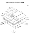
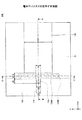
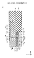
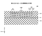
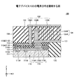
図1は、実施の形態の電子デバイス100を示す斜視図である。図2は、図1におけるA−A矢視断面を示す図である。図3は、電子デバイス100を示す平面図である。図4は、図3におけるB−B矢視断面を示す図である。図5は、図3におけるC−C矢視断面を示す図である。図1乃至図5ではXYZ座標系を定義して説明する。また、図3乃至図5に一例として示す各部の寸法を表す数値の単位は、μmである。図4に示す断面は、図2に示す断面と同一であり、寸法を加えたものである。なお、以下では説明の便宜上、Z軸正方向側を上、Z軸負方向側を下と称すが、普遍的な上下の関係を表すものではない。
<Embodiment>
FIG. 1 is a perspective view illustrating an
電子デバイス100は、半導体チップ110、モールド樹脂120、絶縁層130、接地層131、配線層132、ビア133、及び接地導体134を含む。電子デバイス100は、ウエハに複数の半導体装置及び電子素子等を形成し、半導体製造技術で配線等を形成した後に個片化して半導体チップ及びチップ部品等を作製し、半導体チップ及びチップ部品等をモールド樹脂120でウエハ状に再構築してから再び個片化し、再配線を行ったものである。なお、電子デバイス100は、半導体チップ110に加えて、キャパシタ又はインダクタ等のチップ部品をさらに含んでもよい。
The
電子デバイス100は、FOWLP(Fan Out Wafer Level Package)技術を利用したモジュールであり、バンプを用いることなく、半導体装置及び電子素子等の端子に直接的に配線等を接続することができる。
The
半導体チップ110は、半導体装置111、接地層112、絶縁層113(113A、113B)、配線114、及びビア115を有する。半導体装置111は、一例として、シリコンウエハに形成された半導体装置であり、演算処理又は制御処理等を行う回路等を含む。半導体装置111のZ軸正方向側の面にある信号端子111A及びグランド端子111Bには、それぞれ、配線114及び接地層112が接続される。
The
配線114は、接地層112の開口部112A内に設けられるはんだ114Aを介して信号端子111Aに接続される。開口部112Aは、平面視で円形の開口部である。また、接地層112は、直接的にグランド端子111Bに接続される。なお、はんだを用いて接地層112をグランド端子111Bに接続してもよい。
The
接地層112は、半導体装置111のZ軸正方向側の面に配置されており、半導体製造技術で形成されたものである。接地層112は、第1接地層の一例である。接地層112の幅は、平面視で配線114の幅よりも広く、一例として、半導体チップ110のY軸方向の幅全体にわたって設けられている。
The
接地層112は、半導体装置111のグランド端子111Bに接続され、接地電位に保持される。接地層112のX軸正方向側の端部には、ビア115が接続されている。接地層112の上面及び側面は、絶縁層113のうちの絶縁層113Aによって覆われている。
The
絶縁層113は、絶縁層113A及び113Bを有する。絶縁層113は、チップ絶縁層の一例である。絶縁層113Aは、接地層112を覆っており、絶縁層113Aの上には配線114が配置されている。絶縁層113Aは、例えば、ポリイミド樹脂であり、接地層112と配線114を絶縁する層間絶縁膜である。
The
絶縁層113Bは、配線114の上に配置されており、配線114を覆っている。絶縁層113Bは、例えば、ソルダーレジストである。絶縁層113Bの上面は、半導体チップ110の上面である。絶縁層113Bは、保護絶縁層の一例である。
The
配線114は、絶縁層113Aの上面に形成されている。配線114は、第1配線の一例である。配線114は、一端が半導体装置111の信号端子111Aに接続され、他端がビア133に接続されている。配線114は、半導体製造技術で形成されたものである。配線114は、接地層112とマイクロストリップラインを構築する。配線114の特性インピーダンスは、一例として50Ωに設定される。配線114及び接地層112が構築するマイクロストリップラインは、第1伝送路の一例である。
The
ビア115は、ビア115A、接続部115B、及びビア115Cを有する。ビア115は、半導体製造技術で形成されたものである。ビア115は、下端が接地層112のX軸正方向側の端部に接続され、上端が接地層131のX軸負方向側の端部に接続される。ビア115は、接地層131を接地電位に保持するために設けられている。
The via 115 includes a via 115A, a
モールド樹脂120は、半導体チップ110の側面を覆っている。モールド樹脂120は、半導体チップ及びチップ部品等をウエハ状に再構築するために用いられる。モールド樹脂120は、例えば、エポキシ系の樹脂に球状のシリカフィラー(充填材)を混合させたものである。なお、モールド樹脂120は、半導体チップ110の側面に加えて、上面を覆っていてもよい。
The
絶縁層130は、半導体チップ110及び接地層131の全体の上に配置される。絶縁層130は、再配線層としての接地層131と配線層132を絶縁する層間絶縁膜である。また、絶縁層130には、ビア133と接地導体134が設けられる。絶縁層130は、誘電正接が低い絶縁材料製であればよく、例えば、ポリフェニレンエーテル系材料のフィルム状非感光性材料を用いることができる。
The insulating
接地層131は、半導体チップ110のX軸正方向側の端部と、モールド樹脂120との上に配置される。接地層131の幅は、平面視で配線層132の幅よりも広く、一例として、半導体チップ110及びモールド樹脂120のY軸方向の幅全体にわたって設けられている。また、接地層131のX軸負方向側の端部は、ビア133に近接しており、X軸負方向側の端部の上面には、接地導体134が設けられる。接地層131は、第2接地層の一例である。
The
配線層132は、絶縁層130の上に設けられている。配線層132は、主導体部132Aと、配線部132B及び132Cとを有する。配線層132は、第2配線の一例であり、主導体部132Aは第1部分の一例であり、配線部132B及び132Cは第2部分の一例である。
The
主導体部132Aは、絶縁層130のX軸正方向側の端から平面視で接地導体134の手前まで延在しており、絶縁層130を挟んで接地層131と重ねられている。また、主導体部132Aの幅は、配線部132B及び132Cの幅よりも広く、第1線幅の一例である。主導体部132Aは、接地層131とマイクロストリップラインを構築する。主導体部132Aと接地層131が構築するマイクロストリップラインは、第2伝送路の一例である。主導体部132Aの特性インピーダンスは、一例として50Ωに設定されている。
The
配線部132B及び132Cは、主導体部132AのX軸負方向側の端部から突出するように設けられている。配線部132B及び132Cの幅は、主導体部132Aの幅よりも狭く、第2線幅の一例である。また、配線部132B及び132CのY軸方向における位置は、配線114の位置と合わせられている。
The
配線部132Bは、接地導体134の接続部134Bの上に位置している。配線部132Bは、接続部134B(接地導体134)とマイクロストリップラインを構築する。配線部132Bは、主導体部132Aと接続部134B(接地導体134)との結合を弱めるために、X軸方向において、接続部134BのX軸正方向側の端よりもX軸正方向側に少し延出している。
The
また、配線部132Bは、X軸方向において、接続部134BのX軸負方向側の端よりもX軸負方向側に少し延出している。接続部134B(接地導体134)とマイクロストリップラインを構築できる範囲でX軸負方向側に伸ばすためである。また、配線部132Bの先端には、配線部132Cが設けられている。
In addition, the
配線部132Cは、ビア133の上端に接続されている。配線部132Cの幅は、インピーダンスを調整するために、配線部132Bの幅よりも少しだけ狭くされている。配線部132Cは、配線部132Bのうちの接続部134BのX軸負方向側の端よりもX軸負方向側に少し延出している部分と同様に、接続部134B(接地導体134)とマイクロストリップラインを構築する。
The
配線部132B及び132Cと、接続部134B(接地導体134)とが構築するマイクロストリップラインの特性インピーダンスは、一例として50Ωに設定されている。配線部132B及び132Cと、接続部134B(接地導体134)とが構築するマイクロストリップラインは、第4伝送路の一例である。
The characteristic impedance of the microstrip line constructed by the
ビア133は、絶縁層113Bと絶縁層130とを厚さ方向(Z軸方向)に貫通し、配線114のX軸正方向側の端部と、配線部132Cとの間を接続している。ビア133は、ビア115A、接続部115B、及び接地導体134とマイクロストリップラインを構築する。ビア133の接地導体134よりも高い部分も、接地導体134とマイクロストリップラインを構築する。ビア133と、ビア115A、接続部115B、及び接地導体134とが構築するマイクロストリップラインは、第3伝送路の一例である。
The via 133 penetrates the insulating
接地導体134は、接地層131のX軸負方向側の端部において、Z軸正方向に起立するように、垂直に設けられている。接地導体134は、複数の円柱部134Aと、複数の円柱部134Aの上端を接続する接続部134Bとを有する。
The
複数の円柱部134Aは、Y軸方向に配列されている。ここでは一例として、9本の円柱部134Aを示す。複数の円柱部134Aの下端は接地層131に接続され、上端は接続部134Bによって接続されている。接続部134Bは、数の円柱部134Aの上端を接続し、Y軸方向に延在している。円柱部134Aは、柱状部の一例である。
The plurality of
このような接地導体134は、上述したように、ビア133及び配線部132B及び132CとXZ面視で逆L字型のマイクロストリップラインを構築するために設けられている。9本の円柱部134Aと接続部134Bとによって構築される接地導体134は、接地電位に保持される1つの壁部があることと等価である。
As described above, such a
ここで、図3乃至図5を用いて、各部の寸法について説明する。図3に示すように、接地層112と配線114とのZ軸方向のギャップは10μmである。絶縁層130の厚さは50μmである。すなわち、接地層131と配線層132とのZ軸方向のギャップは50μmである。
Here, the dimension of each part is demonstrated using FIG. 3 thru | or FIG. As shown in FIG. 3, the gap in the Z-axis direction between the
ビア133と、接地導体134の円柱部134AとのX軸方向のギャップは10μmである。ビア133の直径は15μmである。円柱部134Aの直径は20μmである。接続部134BのX軸方向の幅は30μmである。配線層132と接続部134BとのZ軸方向のギャップは10μmである。
The gap in the X-axis direction between the via 133 and the
また、図4に示すように、配線114のY軸方向の幅は23μmである。配線部132CのY軸方向の幅は20μmであり、X軸方向の長さは20μmである。配線部132BのY軸方向の幅は25μmであり、X軸方向の長さは37.5μmである。主導体部132AのY軸方向の幅は140μmである。配線114と、主導体部132A、配線部132B及び132Cは、すべてY軸方向の幅の中心が一致(中心軸が一致)するように配置されている。また、図5に示すように、隣り合う円柱部134A同士のピッチ(中心軸同士の間隔)は25μmである。
Further, as shown in FIG. 4, the width of the
なお、接地層112、配線114、接地層131、及び配線層132の厚さは、0.5μmである。
The thickness of the
電子デバイス100では、配線層132の主導体部132Aにおける電力伝達損失を低減するために、主導体部132Aの線幅を広く取っている。マイクロストリップラインで所定のインピーダンス(ここでは、50Ω)を一定に保つためには、配線の線幅が広くなれば、接地層及び配線のギャップを大きく取る必要がある。
In the
ところで、例えばソルダーレジストのような一般的な液状感光性材料は、誘電正接が300GHzで0.087と大きいため、絶縁層130(50μm)のように厚くすることは困難である。このため、絶縁層130に液状感光性材料を用いると、主導体部132Aの線幅を広く取ることは困難になる。
By the way, a general liquid photosensitive material such as a solder resist has a dielectric loss tangent as large as 0.087 at 300 GHz, and thus it is difficult to make it as thick as the insulating layer 130 (50 μm). For this reason, when a liquid photosensitive material is used for the insulating
そこで、電子デバイス100では、絶縁層130に、誘電正接が小さく、厚膜化が容易なフィルム状非感光性材料を用いることによって、絶縁層130を厚くしている。そして、絶縁層130を厚くした分だけ、主導体部132Aの線幅を広く取り、主導体部132Aにおける電力伝達損失を大幅に低減できる構成にしている。
Therefore, in the
なお、ここでは、配線114と接地層112、ビア133と接地導体134及びビア115、配線層132と接地層131がそれぞれマイクロストリップラインを構築する形態について説明する。これら4つのマイクロストリップラインの特性インピーダンスは、すべて50Ωであるが、50Ωは設計値あるいは理論値であり、各マイクロストリップラインの実際の特性インピーダンスは、50Ωから少しずれている場合が有り得る。このようなずれは、製造誤差又はその他の要因等によって生じうる。しかしながら、このような場合も含めて、4つのマイクロストリップラインの特性インピーダンスは、50Ωで等しいものとして取り扱う。特性インピーダンスが互いに等しいとは、このような意味である。
Here, a mode in which the
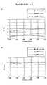
図6は、電磁界解析結果を示す図である。図6(A)にはS11パラメータの周波数特性を示し、図6(B)にはS21パラメータの周波数特性を示す。なお、S11パラメータとS21パラメータは、配線114及び接地層112をポート1、配線層132及び接地層131をポート2として、電磁界解析で求めた。
FIG. 6 is a diagram illustrating the electromagnetic field analysis results. 6A shows the frequency characteristics of the S11 parameter, and FIG. 6B shows the frequency characteristics of the S21 parameter. The S11 parameter and the S21 parameter were obtained by electromagnetic field analysis using the
実施の形態の電子デバイス100の絶縁層130の厚さは50μmであり、配線層132の主導体部132Aの線幅は140μmであり、絶縁層130には誘電正接が300GHzで0.025のフィルム状非感光性材料を用いた。
The thickness of the insulating
また、比較用に、2つの電子デバイス(以下、比較用デバイス1、2と称す)を用意した。比較用デバイス1では、絶縁層130の厚さを10μm、主導体部132Aの線幅を25μmとし、絶縁層130には誘電正接が0.025(300GHz)のフィルム状非感光性材料を用いた。比較用デバイス2では、絶縁層130の厚さを10μm、主導体部132Aの線幅を23μmとし、絶縁層130には誘電正接が0.087(300GHz)の液状感光性材料を用いた。比較用デバイス1、2は、接地導体134を含まない。
For comparison, two electronic devices (hereinafter referred to as
図6(A)に示すように、S11パラメータの周波数特性(反射特性)は、電子デバイス100では−25dB以下で最も低く、比較用デバイス1は、周波数が約240GHz以上で−25dB以上であり、周波数の上昇とともに増大する傾向があった。また、比較用デバイス2では、約−18dB〜約−15dBであり、周波数の上昇とともに増大する傾向があった。
As shown in FIG. 6A, the frequency characteristic (reflection characteristic) of the S11 parameter is the lowest at −25 dB or less in the
図6(B)に示すように、S21パラメータの周波数特性(通過特性)は、電子デバイス100では約−0.5dBであった。比較用デバイス1も約−0.5dBであり、電子デバイス100と同等の値であった。また、比較用デバイス2では、約−0.6dB〜約−0.75dBであり、周波数の上昇とともに低下する傾向があった。
As shown in FIG. 6B, the frequency characteristic (passage characteristic) of the S21 parameter was about −0.5 dB in the
以上のように、電子デバイス100は、比較用デバイス1、2に比べて反射特性及び通過特性ともに良好であった。
As described above, the
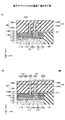
次に、電子デバイス100の製造方法について説明する。図7及び図8は、電子デバイス100の製造工程を示す図である。
Next, a method for manufacturing the
まず、図7(A)に示すように、モールド樹脂120が接合された半導体チップ110を用意する。図7(A)に示す半導体チップ110及びモールド樹脂120は、複数の半導体チップ110を配列し、モールド樹脂120でウエハ状に再構築してから再び個片化したものである。モールド樹脂120は、複数の半導体チップ110を配列した状態で、ウェハの形状に対応した金型を用いて加熱処理を行い、個片化することによって作製される。なお、絶縁層113Bには、後にビア133の下端を形成するための開口部133B1が設けられている。
First, as shown in FIG. 7A, a
次に、図7(B)に示すように、モールド樹脂120の上に接地層131を形成する。接地層131のX軸負方向側の端部の下面は、ビア115Aに接合される。接地層131は、例えば、スパッタ法で電解めっき用のシード層をモールド樹脂120の上に形成し、シード層の上にレジストを形成し、レジストを接地層131の形状にパターニングした後に電解めっき処理を行い、レジストと不要なシード層を除去することによって作製される。
Next, as shown in FIG. 7B, a
次に、図7(C)に示すように、絶縁層130Aを形成する。絶縁層130Aは、図1乃至図5に示す絶縁層130のうち、接地導体134の円柱部134Aの上端までの高さの部分であり、第1絶縁層の一例である。絶縁層130Aは、ポリフェニレンエーテル系材料のフィルム状非感光性材料をラミネート加工で貼り付け、熱処理して硬化させることによって作製される。このとき、開口部113B1は絶縁層130Aで充填される。
Next, as illustrated in FIG. 7C, an insulating
次に、絶縁層130Aに、ビア133Aと複数の円柱部134Aを形成するためのビアホールを形成し、スパッタ法で電解めっき用のシード層をビアホールの内部及び絶縁層130Aの上面に形成し、絶縁層130Aの上面のシード層にレジストを形成し、電解めっき処理を行うことによってビア133A、円柱部134A、及び接続部134Bを作製する。なお、ビアホールは、例えば、エキシマレーザを用いて絶縁層130Aを加工することによって作製すればよい。
Next, a via hole for forming the via 133A and the plurality of
そして、絶縁層130Aの上面のレジストとシード層を除去することにより、図7(D)に示す構造体を得る。円柱部134Aは、所謂ビアの製造方法によって作製される。ここで、ビア133Aは、図1乃至図5に示すビア133のうち、円柱部134Aと同一の高さの部分である。
Then, by removing the resist and the seed layer on the top surface of the insulating
次に、図7(D)に示す構造体の絶縁層130、ビア133A、接続部134Bの上に、図8(A)に示すように、絶縁層130Bを形成する。絶縁層130Bは、絶縁層130Aと同一の材料で、同様の方法によって形成すればよい。絶縁層130Bと絶縁層130Aとの合計の厚さは、図1乃至図5に示す絶縁層130の厚さに等しい。絶縁層130Bは、第2絶縁層の一例である。
Next, as illustrated in FIG. 8A, the insulating
次に、絶縁層130Bに、ビア133Aの上端まで到達するビアホールを形成し、ビアホールの内部及び絶縁層130Bの表面にスパッタ法で電解めっき用のシード層を形成し、シード層の上にレジストを形成し、レジストを配線層132の形状にパターニングした後に電解めっき処理を行い、レジストと不要なシード層を除去することにより、図8(B)に示すように、ビア133B及び配線層132(主導体部132Aと配線部132B及び132C)を作製する。なお、ビアホールは、例えば、エキシマレーザを用いて絶縁層130Bを加工することによって作製すればよい。
Next, a via hole reaching the upper end of the via 133A is formed in the insulating
以上の工程を行うことにより、電子デバイス100が完成する。
By performing the above steps, the
図9は、電子デバイス100の電界分布を説明する図である。図9には、電界の方向を矢印で示す。電子デバイス100では、配線114は、接地層112とマイクロストリップラインを構築し、配線層132の主導体部132Aは、接地層131とマイクロストリップラインを構築する。
FIG. 9 is a diagram illustrating the electric field distribution of the
主導体部132Aの線幅を広くして電力伝達損失を低減するために、絶縁層130として、誘電正接が小さく、厚膜化が容易なフィルム状非感光性材料を用いて絶縁層130の厚さを稼いでいる。
In order to reduce the power transmission loss by widening the line width of the
このように絶縁層130を厚くすると、ビア133がZ軸方向に長くなるので、ビア133の特性インピーダンスを改善することが望ましい。また、配線層132の配線部132B及び132Cの特性インピーダンスを改善することも望ましい。
When the insulating
そこで、電子デバイス100では、ビア133に沿ってZ軸方向に延在する接地導体134を設けている。
Therefore, in the
ビア133は、接地導体134及びビア115とマイクロストリップラインを構築する。ビア133の接地導体134よりも高い部分も、斜めの矢印で示すような電界の分布が得られ、接地導体134とマイクロストリップラインを構築する。また、ビア133の下側の部分も、ビア115A及び接続部115Bとマイクロストリップラインを構築する。
The via 133 forms a microstrip line with the
また、配線層132の配線部132B及び132Cは、接続部134B(接地導体134)とマイクロストリップラインを構築する。配線部132Cと接続部134Bとの間にも、斜めの矢印で示すような電界の分布が得られ、マイクロストリップラインが構築される。
In addition, the
また、接続部115B及びビア115Cと配線114との間にも、斜めの矢印で示すような電界の分布が得られ、マイクロストリップラインが構築される。
In addition, an electric field distribution as shown by oblique arrows is obtained between the connecting
このように、電子デバイス100では、半導体チップ110に、マイクロストリップラインを構築する、配線114、ビア133、配線層132、接地層112、ビア115、接地導体134、及び接地層131が接続されている。
As described above, in the
従って、実施の形態によれば、動作特性の良好な電子デバイス100、及び、電子デバイス100の製造方法を提供することができる。
Therefore, according to the embodiment, it is possible to provide an
また、配線層132の主導体部132Aの線幅は、数100GHz以上の高周波電力が流れる場合においても、電力伝達損失を十分に低減できるほどに拡げられている。
Further, the line width of the
また、電子デバイス100は、絶縁層130として、誘電正接の小さいフィルム状非感光性材料を用いているため、絶縁層130を厚くすることができる。この結果、配線層132の主導体部132Aの線幅を広くすることができ、電力伝達損失を十分に低減することができる。
Further, since the
周波数が300GHzを超えるような超高周波信号は、波長が1mm以下であり、絶縁層130等の誘電率を考慮すると、1/20波長の長さは30μm以下になる。このため、ビア133の長さ(50μm強)は無視することができず、インピーダンス整合を取ることが必要になる。
An ultra-high frequency signal having a frequency exceeding 300 GHz has a wavelength of 1 mm or less, and considering the dielectric constant of the insulating
このような観点から、電子デバイス100は、ビア133に沿って延在する接地導体134を設け、ビア133がマイクロストリップラインを構築する構成にしている。このような構成により、低損失な接続構造を実現している。
From this point of view, the
なお、以上では、半導体チップ110が、半導体装置111の上に設けられる接地層112、絶縁層113(113A、113B)、及び配線114を含む形態について説明したが、半導体チップ110は、さらに他の配線又は接地層を含んでもよい。
In the above description, the
また、モールド樹脂120、絶縁層130、接地層131、及び配線層132は、X軸正方向にさらに延在していてもよく、また、接地層131及び配線層132は、図示しない他の電子装置又は電子部品等に接続されていてもよい。
In addition, the
また、以上では、ビア115が接地層131と接地層112とを接続する形態について説明したが、配線114のX軸正方向側の端部における特性インピーダンスに影響が生じないような場合には、ビア115を設けることなく、別な手段で接地層131をグランド電位に保持するようにしてもよい。
In the above description, the via 115 connects the
また、以上では、接地導体134が、複数の円柱部134Aと、接続部134Bとを有する形態について説明したが、接地導体134は、ビア133及び配線部132B及び132Cとマイクロストリップラインを構築できるのであれば、どのような形状であってもよい。
In the above description, the
また、以上では、接地層131が半導体チップ110と絶縁層130との間に設けられる形態について説明したが、接地層131は、絶縁層130の内部に設けられていてもよい。絶縁層130の内部とは、厚さ方向において、絶縁層130に上下を挟まれる位置である。
In the above description, the
以上、本発明の例示的な実施の形態の電子デバイス、及び、電子デバイスの製造方法について説明したが、本発明は、具体的に開示された実施の形態に限定されるものではなく、特許請求の範囲から逸脱することなく、種々の変形や変更が可能である。 The electronic device and the manufacturing method of the electronic device according to the exemplary embodiments of the present invention have been described above, but the present invention is not limited to the specifically disclosed embodiments, and is claimed. Various modifications and changes can be made without departing from the scope.
以上の実施の形態に関し、さらに以下の付記を開示する。
(付記1)
半導体装置と、前記半導体装置の第1面側に設けられる第1接地層と、所定の特性インピーダンスを有する第1伝送路を前記第1接地層と構築する第1配線とを有する半導体チップと、
前記半導体チップに重ねて配置される絶縁層と、
前記半導体チップと前記絶縁層との間、又は、前記絶縁層の内部に設けられる第2接地層と、
前記絶縁層に重ねて配置される第2配線であって、平面視で前記第2接地層と重なる部分に配置され、第1線幅を有し、前記第1伝送路と等しい所定の特性インピーダンスを有する第2伝送路を前記第2接地層と構築する第1部分と、平面視で前記第2接地層の端部側に配置され、前記第1線幅よりも細い第2線幅を有する第2部分とを有する第2配線と、
前記第1配線と前記第2配線の前記第2部分とを接続するビアと、
平面視で前記第2配線の前記第2部分と重なる位置において前記絶縁層の内部に設けられ、前記第2部分の線幅方向において前記第2部分よりも広い幅を有し、前記ビアに沿って前記第2接地層から前記第2部分の手前まで延在する接地導体と
を含み、
前記ビアは、前記第1伝送路と等しい所定の特性インピーダンスを有する第3伝送路を前記接地導体と構築し、
前記第2配線の前記第2部分は、前記第1伝送路と等しい所定の特性インピーダンスを有する第4伝送路を前記接地導体と構築する、電子デバイス。
(付記2)
前記接地導体は、
一端が前記第2接地層に接続され、前記線幅方向に配置される、複数の柱状部と、
前記線幅方向に延在し、前記複数の柱状部の他端を接続する接続導体と
を有する、付記1記載の電子デバイス。
(付記3)
前記第2接地層は、前記第1接地層に接続される、付記1又は2記載の電子デバイス。
(付記4)
前記半導体チップは、
前記半導体装置の第1面に設けられるチップ絶縁層と、
前記第1配線を覆う保護絶縁層と
をさらに有し、
前記第1接地層は、前記半導体装置と前記チップ絶縁層との間に設けられ、
前記第1配線は、前記チップ絶縁層に重ねて配置される、付記1乃至3のいずれか一項記載の電子デバイス。
(付記5)
前記第1伝送路、前記第2伝送路、前記第3伝送路、及び前記第4伝送路は、マイクロストリップラインである、付記1乃至4のいずれか一項記載の電子デバイス。
(付記6)
半導体装置と、前記半導体装置の第1面側に設けられる第1接地層と、所定の特性インピーダンスを有する第1伝送路を前記第1接地層と構築する第1配線とを有する半導体チップに、平面視で前記第1配線と重ならないように第2接地層を積層する工程と、
前記半導体チップ及び前記第2接地層に重ねて第1絶縁層を形成する工程と、
一端が前記第2接地層の端部に接続され、前記第1絶縁層を厚さ方向に貫通し、前記第1配線よりも広い幅を有する接地導体を形成する工程と、
前記第1絶縁層に重ねて第2絶縁層を形成する工程と、
一端が前記第1配線に接続され、前記第1絶縁層及び前記第2絶縁層を厚さ方向に貫通するとともに前記接地導体に沿って延在し、他端が前記第2絶縁層から表出するビアを形成する工程と、
前記第2絶縁層に重ねて第2配線を形成する工程であって、平面視で前記第2接地層と重なる部分に配置され、第1線幅を有し、前記第1伝送路と等しい所定の特性インピーダンスを有する第2伝送路を前記第2接地層と構築する第1部分と、平面視で前記第2接地層の前記端部側において前記接地導体と重なる位置に配置され、前記第1線幅及び前記接地導体の幅よりも細い第2線幅を有し、前記ビアに接続される第2部分とを有する第2配線を形成する工程と
を含み、
前記ビアは、前記第1伝送路と等しい所定の特性インピーダンスを有する第3伝送路を前記接地導体と構築し、
前記第2配線の前記第2部分は、前記第1伝送路と等しい所定の特性インピーダンスを有する第4伝送路を前記接地導体と構築する、電子デバイスの製造方法。
Regarding the above embodiment, the following additional notes are disclosed.
(Appendix 1)
A semiconductor chip having a semiconductor device, a first ground layer provided on the first surface side of the semiconductor device, and a first wiring for constructing a first transmission line having a predetermined characteristic impedance with the first ground layer;
An insulating layer disposed over the semiconductor chip;
A second ground layer provided between the semiconductor chip and the insulating layer or inside the insulating layer;
A second wiring disposed to overlap the insulating layer, disposed in a portion overlapping the second ground layer in plan view, having a first line width, and having a predetermined characteristic impedance equal to the first transmission line A first portion that constructs a second transmission line having the second ground layer and a second line width that is disposed on an end side of the second ground layer in plan view and is narrower than the first line width A second wiring having a second portion;
A via connecting the first wiring and the second portion of the second wiring;
Provided inside the insulating layer at a position overlapping the second portion of the second wiring in plan view, has a width wider than the second portion in the line width direction of the second portion, and extends along the via And a ground conductor extending from the second ground layer to the front of the second portion,
The via constructs with the ground conductor a third transmission line having a predetermined characteristic impedance equal to the first transmission line;
The electronic device, wherein the second part of the second wiring constructs a fourth transmission line having a predetermined characteristic impedance equal to the first transmission line with the ground conductor.
(Appendix 2)
The ground conductor is
A plurality of columnar portions, one end of which is connected to the second ground layer and disposed in the line width direction;
The electronic device according to
(Appendix 3)
The electronic device according to
(Appendix 4)
The semiconductor chip is
A chip insulating layer provided on the first surface of the semiconductor device;
A protective insulating layer covering the first wiring;
The first ground layer is provided between the semiconductor device and the chip insulating layer,
4. The electronic device according to
(Appendix 5)
The electronic device according to any one of
(Appendix 6)
A semiconductor chip having a semiconductor device, a first ground layer provided on the first surface side of the semiconductor device, and a first wiring for constructing a first transmission line having a predetermined characteristic impedance with the first ground layer, Laminating a second ground layer so as not to overlap the first wiring in plan view;
Forming a first insulating layer overlying the semiconductor chip and the second ground layer;
Forming a ground conductor having one end connected to the end of the second ground layer, penetrating the first insulating layer in the thickness direction, and having a width wider than the first wiring;
Forming a second insulating layer overlying the first insulating layer;
One end is connected to the first wiring, passes through the first insulating layer and the second insulating layer in the thickness direction and extends along the ground conductor, and the other end is exposed from the second insulating layer. Forming a via, and
A step of forming a second wiring over the second insulating layer, the second wiring being disposed in a portion overlapping the second ground layer in plan view, having a first line width and being equal to the first transmission line A first portion that constructs a second transmission line having a characteristic impedance of the second ground layer with the second ground layer, and is disposed at a position overlapping the ground conductor on the end side of the second ground layer in plan view, Forming a second wiring having a line width and a second line width that is smaller than a width of the ground conductor, and a second portion connected to the via,
The via constructs with the ground conductor a third transmission line having a predetermined characteristic impedance equal to the first transmission line;
The method of manufacturing an electronic device, wherein the second part of the second wiring constructs a fourth transmission line having a predetermined characteristic impedance equal to that of the first transmission line with the ground conductor.
100 電子デバイス
110 半導体チップ
111 半導体装置
111A 信号端子
111B グランド端子
112 接地層
113(113A、113B) 絶縁層
114 配線
115 ビア
115A ビア
115B 接続部
115C ビア
120 モールド樹脂
130 絶縁層
131 接地層
132 配線層
132A 主導体部
132B、132C 配線部
133 ビア
134 接地導体
134A 円柱部
134B 接続部
DESCRIPTION OF
Claims (5)
前記半導体チップに重ねて配置される絶縁層と、
前記半導体チップと前記絶縁層との間、又は、前記絶縁層の内部に設けられる第2接地層と、
前記絶縁層に重ねて配置される第2配線であって、平面視で前記第2接地層と重なる部分に配置され、第1線幅を有し、前記第1伝送路と等しい所定の特性インピーダンスを有する第2伝送路を前記第2接地層と構築する第1部分と、平面視で前記第2接地層の端部側に配置され、前記第1線幅よりも細い第2線幅を有する第2部分とを有する第2配線と、
前記第1配線と前記第2配線の前記第2部分とを接続するビアと、
平面視で前記第2配線の前記第2部分と重なる位置において前記絶縁層の内部に設けられ、前記第2部分の線幅方向において前記第2部分よりも広い幅を有し、前記ビアに沿って前記第2接地層から前記第2部分の手前まで延在する接地導体と
を含み、
前記ビアは、前記第1伝送路と等しい所定の特性インピーダンスを有する第3伝送路を前記接地導体と構築し、
前記第2配線の前記第2部分は、前記第1伝送路と等しい所定の特性インピーダンスを有する第4伝送路を前記接地導体と構築する、電子デバイス。 A semiconductor chip having a semiconductor device, a first ground layer provided on the first surface side of the semiconductor device, and a first wiring for constructing a first transmission line having a predetermined characteristic impedance with the first ground layer;
An insulating layer disposed over the semiconductor chip;
A second ground layer provided between the semiconductor chip and the insulating layer or inside the insulating layer;
A second wiring disposed to overlap the insulating layer, disposed in a portion overlapping the second ground layer in plan view, having a first line width, and having a predetermined characteristic impedance equal to the first transmission line A first portion that constructs a second transmission line having the second ground layer and a second line width that is disposed on an end side of the second ground layer in plan view and is narrower than the first line width A second wiring having a second portion;
A via connecting the first wiring and the second portion of the second wiring;
Provided inside the insulating layer at a position overlapping the second portion of the second wiring in plan view, has a width wider than the second portion in the line width direction of the second portion, and extends along the via And a ground conductor extending from the second ground layer to the front of the second portion,
The via constructs with the ground conductor a third transmission line having a predetermined characteristic impedance equal to the first transmission line;
The electronic device, wherein the second part of the second wiring constructs a fourth transmission line having a predetermined characteristic impedance equal to the first transmission line with the ground conductor.
一端が前記第2接地層に接続され、前記線幅方向に配置される、複数の柱状部と、
前記線幅方向に延在し、前記複数の柱状部の他端を接続する接続導体と
を有する、請求項1記載の電子デバイス。 The ground conductor is
A plurality of columnar portions, one end of which is connected to the second ground layer and disposed in the line width direction;
The electronic device according to claim 1, further comprising: a connecting conductor that extends in the line width direction and connects the other ends of the plurality of columnar portions.
前記半導体装置の第1面に設けられるチップ絶縁層と、
前記第1配線を覆う保護絶縁層と
をさらに有し、
前記第1接地層は、前記半導体装置と前記チップ絶縁層との間に設けられ、
前記第1配線は、前記チップ絶縁層に重ねて配置される、請求項1乃至3のいずれか一項記載の電子デバイス。 The semiconductor chip is
A chip insulating layer provided on the first surface of the semiconductor device;
A protective insulating layer covering the first wiring;
The first ground layer is provided between the semiconductor device and the chip insulating layer,
4. The electronic device according to claim 1, wherein the first wiring is disposed so as to overlap the chip insulating layer. 5.
前記半導体チップ及び前記第2接地層に重ねて第1絶縁層を形成する工程と、
一端が前記第2接地層の端部に接続され、前記第1絶縁層を厚さ方向に貫通し、前記第1配線よりも広い幅を有する接地導体を形成する工程と、
前記第1絶縁層に重ねて第2絶縁層を形成する工程と、
一端が前記第1配線に接続され、前記第1絶縁層及び前記第2絶縁層を厚さ方向に貫通するとともに前記接地導体に沿って延在し、他端が前記第2絶縁層から表出するビアを形成する工程と、
前記第2絶縁層に重ねて第2配線を形成する工程であって、平面視で前記第2接地層と重なる部分に配置され、第1線幅を有し、前記第1伝送路と等しい所定の特性インピーダンスを有する第2伝送路を前記第2接地層と構築する第1部分と、平面視で前記第2接地層の前記端部側において前記接地導体と重なる位置に配置され、前記第1線幅及び前記接地導体の幅よりも細い第2線幅を有し、前記ビアに接続される第2部分とを有する第2配線を形成する工程と
を含み、
前記ビアは、前記第1伝送路と等しい所定の特性インピーダンスを有する第3伝送路を前記接地導体と構築し、
前記第2配線の前記第2部分は、前記第1伝送路と等しい所定の特性インピーダンスを有する第4伝送路を前記接地導体と構築する、電子デバイスの製造方法。 A semiconductor chip having a semiconductor device, a first ground layer provided on the first surface side of the semiconductor device, and a first wiring for constructing a first transmission line having a predetermined characteristic impedance with the first ground layer, Laminating a second ground layer so as not to overlap the first wiring in plan view;
Forming a first insulating layer overlying the semiconductor chip and the second ground layer;
Forming a ground conductor having one end connected to the end of the second ground layer, penetrating the first insulating layer in the thickness direction, and having a width wider than the first wiring;
Forming a second insulating layer overlying the first insulating layer;
One end is connected to the first wiring, passes through the first insulating layer and the second insulating layer in the thickness direction and extends along the ground conductor, and the other end is exposed from the second insulating layer. Forming a via, and
A step of forming a second wiring over the second insulating layer, the second wiring being disposed in a portion overlapping the second ground layer in plan view, having a first line width and being equal to the first transmission line A first portion that constructs a second transmission line having a characteristic impedance of the second ground layer with the second ground layer, and is disposed at a position overlapping the ground conductor on the end side of the second ground layer in plan view, Forming a second wiring having a line width and a second line width that is smaller than a width of the ground conductor, and a second portion connected to the via,
The via constructs with the ground conductor a third transmission line having a predetermined characteristic impedance equal to the first transmission line;
The method of manufacturing an electronic device, wherein the second part of the second wiring constructs a fourth transmission line having a predetermined characteristic impedance equal to that of the first transmission line with the ground conductor.
Priority Applications (2)
| Application Number | Priority Date | Filing Date | Title |
|---|---|---|---|
| JP2017135647A JP6866789B2 (en) | 2017-07-11 | 2017-07-11 | Electronic devices and methods for manufacturing electronic devices |
| US16/019,004 US10283464B2 (en) | 2017-07-11 | 2018-06-26 | Electronic device and manufacturing method of electronic device |
Applications Claiming Priority (1)
| Application Number | Priority Date | Filing Date | Title |
|---|---|---|---|
| JP2017135647A JP6866789B2 (en) | 2017-07-11 | 2017-07-11 | Electronic devices and methods for manufacturing electronic devices |
Publications (2)
| Publication Number | Publication Date |
|---|---|
| JP2019021663A true JP2019021663A (en) | 2019-02-07 |
| JP6866789B2 JP6866789B2 (en) | 2021-04-28 |
Family
ID=64999162
Family Applications (1)
| Application Number | Title | Priority Date | Filing Date |
|---|---|---|---|
| JP2017135647A Active JP6866789B2 (en) | 2017-07-11 | 2017-07-11 | Electronic devices and methods for manufacturing electronic devices |
Country Status (2)
| Country | Link |
|---|---|
| US (1) | US10283464B2 (en) |
| JP (1) | JP6866789B2 (en) |
Cited By (1)
| Publication number | Priority date | Publication date | Assignee | Title |
|---|---|---|---|---|
| WO2023119706A1 (en) * | 2021-12-21 | 2023-06-29 | 株式会社フジクラ | Transmission line |
Families Citing this family (2)
| Publication number | Priority date | Publication date | Assignee | Title |
|---|---|---|---|---|
| DE102019115307A1 (en) | 2019-06-06 | 2020-12-10 | Infineon Technologies Ag | Semi-conductor devices with planar waveguide transmission lines |
| JP7658960B2 (en) * | 2020-05-14 | 2025-04-08 | 住友電工デバイス・イノベーション株式会社 | Semiconductor Device |
Citations (4)
| Publication number | Priority date | Publication date | Assignee | Title |
|---|---|---|---|---|
| JPH0951208A (en) * | 1995-08-07 | 1997-02-18 | Taiyo Yuden Co Ltd | Multi-layer board |
| JP2006211070A (en) * | 2005-01-26 | 2006-08-10 | Hirose Electric Co Ltd | Multilayer wiring board |
| JP2007134359A (en) * | 2005-11-08 | 2007-05-31 | Casio Comput Co Ltd | Semiconductor device and manufacturing method thereof |
| JP2012222182A (en) * | 2011-04-11 | 2012-11-12 | Sony Corp | Semiconductor device |
Family Cites Families (11)
| Publication number | Priority date | Publication date | Assignee | Title |
|---|---|---|---|---|
| US5184095A (en) * | 1991-07-31 | 1993-02-02 | Hughes Aircraft Company | Constant impedance transition between transmission structures of different dimensions |
| JP3313250B2 (en) | 1994-09-06 | 2002-08-12 | 新光電気工業株式会社 | Substrate for mounting high frequency devices |
| JP3500268B2 (en) * | 1997-02-27 | 2004-02-23 | 京セラ株式会社 | High frequency input / output terminal and high frequency semiconductor element storage package using the same |
| JP2000243754A (en) | 1999-02-24 | 2000-09-08 | Sanyo Electric Co Ltd | Semiconductor device |
| US6781488B2 (en) * | 2001-03-27 | 2004-08-24 | Sumitomo Metal (Smi) Electronics Devices Inc. | Connected construction of a high-frequency package and a wiring board |
| WO2009037918A1 (en) * | 2007-09-18 | 2009-03-26 | Nec Corporation | High frequency substrate and high frequency module using same |
| JP2010135722A (en) * | 2008-11-05 | 2010-06-17 | Toshiba Corp | Semiconductor device |
| JP5340188B2 (en) | 2010-01-26 | 2013-11-13 | 京セラ株式会社 | Wiring board |
| JP5636834B2 (en) * | 2010-09-10 | 2014-12-10 | 富士通株式会社 | High frequency circuit package and high frequency circuit device |
| CN104364897B (en) * | 2012-10-29 | 2017-07-25 | 京瓷株式会社 | Element storage packaging part and assembling structure |
| US9196951B2 (en) * | 2012-11-26 | 2015-11-24 | International Business Machines Corporation | Millimeter-wave radio frequency integrated circuit packages with integrated antennas |
-
2017
- 2017-07-11 JP JP2017135647A patent/JP6866789B2/en active Active
-
2018
- 2018-06-26 US US16/019,004 patent/US10283464B2/en active Active
Patent Citations (4)
| Publication number | Priority date | Publication date | Assignee | Title |
|---|---|---|---|---|
| JPH0951208A (en) * | 1995-08-07 | 1997-02-18 | Taiyo Yuden Co Ltd | Multi-layer board |
| JP2006211070A (en) * | 2005-01-26 | 2006-08-10 | Hirose Electric Co Ltd | Multilayer wiring board |
| JP2007134359A (en) * | 2005-11-08 | 2007-05-31 | Casio Comput Co Ltd | Semiconductor device and manufacturing method thereof |
| JP2012222182A (en) * | 2011-04-11 | 2012-11-12 | Sony Corp | Semiconductor device |
Cited By (3)
| Publication number | Priority date | Publication date | Assignee | Title |
|---|---|---|---|---|
| WO2023119706A1 (en) * | 2021-12-21 | 2023-06-29 | 株式会社フジクラ | Transmission line |
| JPWO2023119706A1 (en) * | 2021-12-21 | 2023-06-29 | ||
| JP7598490B2 (en) | 2021-12-21 | 2024-12-11 | 株式会社フジクラ | Transmission Lines |
Also Published As
| Publication number | Publication date |
|---|---|
| US10283464B2 (en) | 2019-05-07 |
| US20190019767A1 (en) | 2019-01-17 |
| JP6866789B2 (en) | 2021-04-28 |
Similar Documents
| Publication | Publication Date | Title |
|---|---|---|
| CN101095380B (en) | Multilayer printed circuit boards including through connections for high frequency applications | |
| JP4544181B2 (en) | Electronic substrate, semiconductor device and electronic equipment | |
| US8119931B1 (en) | Differential vertical structure for high density, low layer count packages | |
| US10806033B2 (en) | Interposer and electronic device | |
| CN102881680B (en) | Semiconductor device and method of manufacturing same | |
| US10389006B2 (en) | Electronic apparatus and manufacturing method thereof | |
| CN104425422A (en) | Functionalised redistribution layer | |
| CN111564426B (en) | RF front-end module, RF communication device and electronic equipment | |
| CN106328597A (en) | Electronic apparatus operable in high frequencies | |
| JP6866789B2 (en) | Electronic devices and methods for manufacturing electronic devices | |
| CN101610636B (en) | Electromagnetic bandgap structure, and printed circuit board | |
| TW202121643A (en) | Vertical interconnection structure of a multi-layer substrate | |
| JP2015141959A (en) | High frequency module | |
| JP5728101B1 (en) | MMIC integrated circuit module | |
| US10879158B2 (en) | Split conductive pad for device terminal | |
| US20220375885A1 (en) | Flip-chip ball grid array-type integrated circuit package for very high frequency operation | |
| US9431337B2 (en) | Semiconductor device having an inner power supply plate structure | |
| US11335614B2 (en) | Electric component embedded structure | |
| CN102341895B (en) | Semiconductor chip and semiconductor device | |
| JP2010021468A (en) | Circuit substrate, and manufacturing method thereof | |
| JP2013197435A (en) | Wiring substrate | |
| CN117238875A (en) | interdigital capacitor | |
| WO2019220530A1 (en) | Signal transmitting structure, method for manufacturing signal transmitting structure, and high-frequency signal transmitting/receiving device | |
| CN110911835B (en) | Antenna device and manufacturing method thereof | |
| JP5083360B2 (en) | Electronic substrate, semiconductor device and electronic equipment |
Legal Events
| Date | Code | Title | Description |
|---|---|---|---|
| A621 | Written request for application examination |
Free format text: JAPANESE INTERMEDIATE CODE: A621 Effective date: 20200409 |
|
| TRDD | Decision of grant or rejection written | ||
| A977 | Report on retrieval |
Free format text: JAPANESE INTERMEDIATE CODE: A971007 Effective date: 20210210 |
|
| A01 | Written decision to grant a patent or to grant a registration (utility model) |
Free format text: JAPANESE INTERMEDIATE CODE: A01 Effective date: 20210309 |
|
| A61 | First payment of annual fees (during grant procedure) |
Free format text: JAPANESE INTERMEDIATE CODE: A61 Effective date: 20210322 |
|
| R150 | Certificate of patent or registration of utility model |
Ref document number: 6866789 Country of ref document: JP Free format text: JAPANESE INTERMEDIATE CODE: R150 |
|
| R250 | Receipt of annual fees |
Free format text: JAPANESE INTERMEDIATE CODE: R250 |
|
| R250 | Receipt of annual fees |
Free format text: JAPANESE INTERMEDIATE CODE: R250 |
|
| S111 | Request for change of ownership or part of ownership |
Free format text: JAPANESE INTERMEDIATE CODE: R313113 |
|
| R350 | Written notification of registration of transfer |
Free format text: JAPANESE INTERMEDIATE CODE: R350 |
|
| R250 | Receipt of annual fees |
Free format text: JAPANESE INTERMEDIATE CODE: R250 |