JP2019021399A - Electrical component socket - Google Patents
Electrical component socket Download PDFInfo
- Publication number
- JP2019021399A JP2019021399A JP2017135918A JP2017135918A JP2019021399A JP 2019021399 A JP2019021399 A JP 2019021399A JP 2017135918 A JP2017135918 A JP 2017135918A JP 2017135918 A JP2017135918 A JP 2017135918A JP 2019021399 A JP2019021399 A JP 2019021399A
- Authority
- JP
- Japan
- Prior art keywords
- latch
- pusher
- electrical component
- socket
- housing portion
- Prior art date
- Legal status (The legal status is an assumption and is not a legal conclusion. Google has not performed a legal analysis and makes no representation as to the accuracy of the status listed.)
- Pending
Links
Images


Abstract
Description
この発明は、半導体装置(以下「ICパッケージ」という)等の電気部品に電気的に接続される電気部品用ソケットに関するものである。 The present invention relates to an electrical component socket that is electrically connected to an electrical component such as a semiconductor device (hereinafter referred to as an “IC package”).
従来、この種の電気部品用ソケットとしては、コンタクトピンが配置されたICソケットが知られている。このようなICソケットの中には、配線基板上に配置されると共に、検査対象であるICパッケージが収容部に収容され、ラッチでICパッケージの上面を押さえることで、このICパッケージの端子と、配線基板の電極とが、コンタクトピンを介して電気的に接続されるものがある。そして、このような状態で導通試験等の試験を行うものである。 Conventionally, as this type of electrical component socket, an IC socket in which contact pins are arranged is known. In such an IC socket, an IC package to be inspected is housed in a housing portion while being placed on a wiring board, and by holding the upper surface of the IC package with a latch, Some of the electrodes of the wiring board are electrically connected via contact pins. Then, a test such as a continuity test is performed in such a state.
ところで、試験を行うICパッケージの中には、その大きさにばらつきがあるものがあり、そのまま試験を行おうとすると、収容部の中でガタついて接触不良が生じ、正常な試験を行うことができない場合があった。そこで、ラッチの開閉動作を操作する操作部材を使ってプッシャを移動させて収容部に収容されたICパッケージを押圧し、当該ICパッケージの位置決めを行うものが提案されていた(例えば、特許文献1参照)。 By the way, some IC packages to be tested vary in size, and if the test is performed as it is, rattling occurs in the housing and a contact failure occurs, and a normal test cannot be performed. There was a case. In view of this, there has been proposed one that positions the IC package by pressing the IC package housed in the housing portion by moving the pusher using an operation member that manipulates the opening / closing operation of the latch (for example, Patent Document 1). reference).
しかしながら、ラッチの開閉動作を操作する操作部材を使ってプッシャを移動させて収容部に収容されたICパッケージの位置決めを行う場合には、プッシャを設置するにあたってラッチの配置箇所を避ける必要があり、設置箇所に制限があった。また、ラッチを避けてプッシャを設置しようとすると、その分だけプッシャ設置の為の箇所が必要となり、ICソケットが大型化してしまう虞があった。 However, when positioning the IC package accommodated in the accommodating portion by moving the pusher using an operation member that manipulates the opening / closing operation of the latch, it is necessary to avoid the location of the latch when installing the pusher, There were restrictions on the installation location. Further, when trying to install the pusher while avoiding the latch, there is a need for a portion for installing the pusher, and the IC socket may be increased in size.
そこで、この発明は、ラッチの開閉動作を操作する操作部材の動作でなくラッチの動作によって作動するプッシャを設置することで、コンパクトな外形を保ちつつ、電気部品(ICパッケージ)毎に外形寸法にばらつきがあるものに対して、所定位置に位置決めすることができる電気部品用ソケット(ICソケット)を提供することを課題としている。 Therefore, according to the present invention, by installing a pusher that operates not by the operation of the operation member that operates the opening / closing operation of the latch but by the operation of the latch, the external dimensions are maintained for each electric component (IC package) while maintaining a compact external shape. An object of the present invention is to provide an electrical component socket (IC socket) that can be positioned at a predetermined position with respect to variations.
かかる課題を達成するために、請求項1に記載の発明は、電気部品を収容する収容部と、該収容部に収容された前記電気部品の端子に電気的に接続されるコンタクトピンと、軸を中心に回動することで開閉動作を行って閉じた状態で前記電気部品の上面を押圧するラッチとを有するソケット本体と、該ソケット本体に対して上下動自在に設けられて前記ラッチの開閉動作を操作する操作部材と、が設けられた電気部品用ソケットにおいて、前記ラッチの開閉動作によって移動させられて、前記ラッチが閉じたときに、前記収容部に収容された前記電気部品の側面を押圧して前記電気部品の位置決めをするプッシャを有しており、前記プッシャが、前記ラッチの前記軸より前記収容部の中心側に配設されている電気部品用ソケットとしたことを特徴とする。
In order to achieve such an object, the invention described in
また、請求項2に記載の発明は、請求項1に記載の発明に加えて、前記ラッチが前記電気部品の前記上面を押圧する前に、前記プッシャで前記電気部品の前記側面を押圧するように構成されている電気部品用ソケットとしたことを特徴とする。 According to a second aspect of the present invention, in addition to the first aspect of the present invention, the pusher pushes the side surface of the electrical component before the latch presses the upper surface of the electrical component. It is set as the socket for electrical components comprised by these.
また、請求項3に記載の発明は、請求項1又は2に記載の発明に加えて、前記プッシャを前記収容部の中心方向に向かって付勢する付勢手段を有しており、前記ラッチが開く方向に回動するにつれて、前記ラッチに設けられた作用部が前記プッシャに設けられた被作用部に係合して、前記付勢手段の付勢力に抗して前記プッシャを前記収容部の外側方向に向かって引っ張り、前記ラッチが閉じる方向に回動するにつれて、前記作用部による前記被作用部への係合が解除されて、前記付勢手段の付勢力によって前記プッシャが前記収容部の前記中心方向に向かって移動するように構成された電気部品用ソケットとしたことを特徴とする。
In addition to the invention described in
また、請求項4に記載の発明は、請求項3に記載の発明に加えて、前記収容部は略方形状を呈しており、前記ラッチは前記収容部の両側部に対向して設けられており、一方の前記ラッチ側に前記プッシャが設けられており、前記ラッチが閉じる方向に回動したときに、前記付勢手段の付勢力によって前記プッシャが前記電気部品の前記側面を前記収容部の前記中心方向に押圧するように構成されており、前記ラッチが設けられた前記収容部の前記両側部と略直交する方向の前記収容部の両側部の一方に、前記操作部材の上下動によって移動させられる第2プッシャが設けられており、該第2プッシャを前記プッシャと略直交する方向で前記収容部の中心方向に向かって付勢する第2付勢手段が設けられており、前記操作部材が下降すると、該操作部材に設けられた第2作用部が前記第2プッシャに設けられた第2被作用部に係合して、前記第2付勢手段の付勢力に抗して前記第2プッシャを前記収容部の外側方向に向かって押し出し、前記電気部品の前記側面から前記第2プッシャを離間させ、前記操作部材が上昇すると、前記第2作用部による前記第2被作用部への係合が解除されて、前記第2付勢手段の付勢力によって前記第2プッシャが前記収容部の前記中心方向に向かって移動し、前記電気部品の前記側面を押圧するように構成されており、前記操作部材を上昇させて前記ラッチを閉じる方向に回動させたときに、前記付勢手段と前記第2付勢手段とで前記プッシャと前記第2プッシャを略直交する方向に移動させて前記電気部品の前記側面を押圧して、前記電気部品の片寄せを行って位置決めするように構成されている電気部品用ソケットとしたことを特徴とする。 According to a fourth aspect of the present invention, in addition to the third aspect of the invention, the accommodating portion has a substantially square shape, and the latch is provided to face both side portions of the accommodating portion. The pusher is provided on one of the latch sides, and when the latch is rotated in the closing direction, the pusher causes the side surface of the electrical component to be moved by the biasing force of the biasing means. It is configured to press in the central direction, and is moved to one of the both side portions of the housing portion in a direction substantially orthogonal to the both side portions of the housing portion provided with the latch by the vertical movement of the operation member. And a second urging means for urging the second pusher in a direction substantially perpendicular to the pusher toward the center of the housing portion, and the operation member. When the A second acting part provided on the working member engages with a second acting part provided on the second pusher, and the second pusher is accommodated against the urging force of the second urging means. When the second pusher is pushed away from the side surface of the electrical component and the operation member is lifted, the second action part is disengaged from the second actuated part. The second pusher is moved toward the central direction of the housing portion by the urging force of the second urging means, and presses the side surface of the electrical component. When the latch is closed and rotated in the closing direction, the pusher and the second pusher are moved in a direction substantially perpendicular to each other by the biasing means and the second biasing means. A piece of the electrical component pressing the side It was characterized by being a socket for electrical parts that are configured to position performed.
また、請求項5に記載の発明は、請求項3に記載の発明に加えて、前記収容部は略方形状を呈しており、前記ラッチは、前記収容部の両側部に対向して設けられると共に、それらと略直交する方向の前記収容部の両側部にも対向して設けられており、前記収容部の略直交する方向の前記両側部のそれぞれ一方の前記ラッチ側に前記プッシャが設けられており、それぞれの前記ラッチが閉じる方向に回動したときに、それぞれの前記プッシャを付勢する前記付勢手段それぞれの付勢力によってそれぞれの前記プッシャを略直交する方向に移動させて、前記電気部品の前記側面を略直交する前記収容部の前記中心方向に押圧して、前記電気部品の片寄せを行って位置決めするように構成されている電気部品用ソケットとしたことを特徴とする。 According to a fifth aspect of the present invention, in addition to the third aspect of the invention, the accommodating portion has a substantially square shape, and the latch is provided to face both side portions of the accommodating portion. In addition, the pusher is provided on both side portions of the housing portion in a direction substantially perpendicular to them, and the pusher is provided on each of the latch sides of the both side portions in the direction substantially perpendicular to the housing portion. And when the respective latches are rotated in the closing direction, the respective pushers are moved in a substantially orthogonal direction by the respective urging forces of the respective urging means for urging the respective pushers. The electrical component socket is configured such that the side surface of the component is pressed in the center direction of the accommodating portion that is substantially orthogonal, and the electrical component is shifted and positioned.
請求項1に記載の発明によれば、ラッチの開閉動作によって移動させられてラッチが閉じたときに電気部品の側面を押圧して位置決めをするプッシャを有しており、プッシャがラッチの軸より収容部の中心側に配設されていることで、コンパクトな外形を保ちつつ、電気部品毎に外形寸法にばらつきがあるものに対して、所定位置に位置決めすることができる。 According to the first aspect of the present invention, the pusher is positioned by pressing the side surface of the electric component when the latch is closed by being moved by the opening / closing operation of the latch, and the pusher is moved from the axis of the latch. By being disposed on the center side of the housing portion, it is possible to position the electrical component at a predetermined position with respect to the electrical component having a variation in the external dimension while maintaining a compact external shape.
請求項2に記載の発明によれば、プッシャが電気部品の側面を押圧して位置決めを完了してから、ラッチで電気部品の上面を押圧するように構成されていることで、スムーズに電気部品の位置決めから保持までを行うことができる。 According to the second aspect of the present invention, the pusher presses the side surface of the electrical component to complete positioning, and then the latch presses the upper surface of the electrical component so that the electrical component smoothly. From positioning to holding can be performed.
請求項3に記載の発明によれば、プッシャの押す動作を付勢手段の付勢力を用いて行い、プッシャの引く動作をラッチの動作を利用して行うことで、プッシャの動作を円滑に行うことができる。 According to the third aspect of the present invention, the pushing operation of the pusher is performed using the urging force of the urging means, and the pulling operation of the pusher is performed using the operation of the latch, thereby smoothly performing the pusher operation. be able to.
請求項4に記載の発明によれば、電気部品に対して対向する両側の上面を押圧するラッチを有している場合に、ラッチが閉じる方向に回動することで電気部品を収容部の中心方向に押圧するプッシャと、操作部材の上昇によって電気部品を収容部のプッシャが押圧する方向と略直交する方向に押圧する第2プッシャとで、片寄せを行うようになっているため、片寄せを確実に行うことができる。 According to the fourth aspect of the present invention, in the case where the latch that presses the upper surfaces on both sides facing the electrical component is provided, the electrical component is placed in the center of the housing portion by rotating the latch in the closing direction. Since the pusher that presses in the direction and the second pusher that presses the electrical component in a direction substantially perpendicular to the direction in which the pusher of the housing portion presses due to the operation member rising, Can be performed reliably.
請求項5に記載の発明によれば、電気部品に対してその周囲の4辺全ての側の上面を押圧するラッチを有している場合に、ラッチが閉じる方向に回動することで電気部品を収容部の略直交する方向の中心方向に押圧する2つのプッシャを有しているため、コンパクトかつラッチの動作に応じて片寄せを確実に行うことができる。 According to the fifth aspect of the present invention, when the electric component has a latch that presses the upper surfaces of all four sides around the electric component, the electric component is turned by rotating the latch in the closing direction. Since the two pushers are pressed in the center direction in the direction substantially orthogonal to the housing portion, the pusher is compact and can be surely shifted according to the operation of the latch.
以下、この発明の実施の形態について説明する。 Embodiments of the present invention will be described below.
図1〜図8には、この発明の実施の形態を示す。 1 to 8 show an embodiment of the present invention.
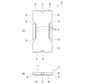
この実施の形態の「電気部品用ソケット」としてのICソケット10は、図1〜図5に示すように、配線基板1上に配置され、上面に「電気部品」としてのICパッケージ2が収容されて、配線基板1の電極(図示省略)とICパッケージ2の端子4に接触して両者を電気的に接続させるように構成されている。そして、このICソケット10は、例えばICパッケージ2に対するバーンイン試験等の導通試験の試験装置などに用いられる。
As shown in FIGS. 1 to 5, an
この実施の形態のICパッケージ2は、主にセラミックで形成されたものであり、図8に示すように、略方形状のパッケージ本体3の下面8の所定位置に、複数の端子4が設けられている。また、パッケージ本体3の側面6に複数の凹部5が設けられている。この実施の形態では、パッケージ本体3の2つの長辺に凹部5が2つずつ設けられており、パッケージ本体3の2つの短辺に凹部5が1つずつ設けられている。なお、この実施の形態のICパッケージ2は、パッケージ本体3の大きさ及び形状が各ICパッケージ2でばらつきがあるものであり、その中で凹部5の位置関係と大きさについては、比較的ばらつきが小さい状態となっているものである。
The
また、ICソケット10は、図2〜図5に示すように、配線基板1上に配置されてICパッケージ2を収容するように構成されたソケット本体20と、ソケット本体の上方に配置された枠形状の操作部材30とを有している。
As shown in FIGS. 2 to 5, the
このうち、ソケット本体20は、ベース部21とフローティング部25とを有している。また、ベース部21からフローティング部25に掛けて、ICパッケージ2の端子4と接触する複数のコンタクトピン50が配設されている。
Among these, the
さらに、ベース部21には、開閉動作を行って閉じた状態(以下、閉状態という)で収容されたICパッケージ2の上面7を押さえて固定する第1ラッチ41,第2ラッチ45が設けられている。また、このソケット本体20の上方に、上下動させることで第1ラッチ41,第2ラッチ45の開閉動作を操作する操作部材30が配設されている。
Further, the
詳述すると、ソケット本体20は、図1に示すように、平面視略方形状を呈しており、配線基板1上に配置されるベース部21の上側にフローティング部25が配設されており、このフローティング部25の上面に、ICパッケージ2を収容する略方形状の収容部26を有している。フローティング部25は、ベース部21に対して上下動自在に構成されており、かつ、ベース部21に対して付勢手段(図示省略)で上方に付勢された状態となっている。また、フローティング部25の収容部26の側の1つ(後述するプッシャ61が配設された側と対向する長辺側)には、2つのガイドピン27が収容部26の中央方向に突出するように設けられている。また、フローティング部25の収容部26の側の他の1つ(後述する第2プッシャ71が配設された側と対向する短辺側)には、1つのガイドピン28が収容部26の中央方向に突出するように設けられている。これらガイドピン27,28は、ICパッケージ2の凹部5に挿入されるような位置に形成されており、その長さが凹部5の奥行きよりも長く、その幅が凹部5の幅より小さく形成されている。
Specifically, as shown in FIG. 1, the
また、コンタクトピン50は、一端部51が収容部26に収容されたICパッケージ2の端子4に接触し、他端部52が配線基板1の電極に接触して、双方を導通させるように構成されており、フローティング部25の上下動によって、一端部51が上下動するように構成されている。
In addition, the
また、ベース部21には、第1ラッチ41,第2ラッチ45が配設されている。この実施の形態の第1ラッチ41,第2ラッチ45は、図1,図3〜図5に示すように、収容部26を挟んで両側に対向する位置に、第1ラッチ41と第2ラッチ45とを有する構成となっている。そして、後述する操作部材30の上下動に応じて、第1ラッチ41と第2ラッチ45とがソケット本体20の所定位置に係合された軸41a,45aを中心として回動することで開閉動作を行うようになっており、これにより収容部26を開いた状態(以下、開状態という)と閉状態にさせるように構成されている。
The
すなわち、第1ラッチ41と第2ラッチ45の双方は、図3に示すように、第1ラッチ41と第2ラッチ45とが内側に回動すると閉状態となって、収容部26に収容されたICパッケージ2の上面7を押圧する状態となり、図5に示すように、第1ラッチ41と第2ラッチ45とが外側に回動すると開状態となって、収容部26にICパッケージ2を収容可能な状態又は収容部26に収容されたICパッケージ2の押圧を解除して取り出し可能な状態となるように構成されている。
That is, both the
以下、第1ラッチ41,第2ラッチ45についてさらに詳述する。なお、第1ラッチ41と第2ラッチ45とは、略同形状で左右逆に配置されたものであるため、詳しい説明は第1ラッチ41のみについて行い、第2ラッチ45の詳しい説明は省略する。
Hereinafter, the
図6に示すように、第1ラッチ41には、略筒状の第1軸受部43aと、同じく略筒状の第3軸受部43cと、略板状の第2軸受部43bとが略直線状に設けられている。また、第1軸受部43aには第1貫通孔43e、第2軸受部43bには第2貫通孔43f、第3軸受部43cには第3貫通孔43gを有しており、これらの貫通孔43e,43f,43gに軸41aを貫通させるようになっている。
As shown in FIG. 6, the
このうち、中央の第2軸受部43bの貫通孔43fは、第2軸受部43bが略板状であるため、両端の第1軸受部43aの第1貫通孔43eと第3軸受部43cの第3貫通孔43gより短い貫通孔に形成されている。また、中央の第2軸受部43bは、両端の第1軸受部43aと第3軸受部43cより直径方向に幅広の略板状に形成されている。
Among these, the through-
また、中央の第2軸受部43bには、その両側の第1軸受部43a側と第3軸受部43c側の面に突出部44を有している。この突出部44は、図3〜図6に示すように、第2軸受部43bの外周部43dと面一となるように略円弧形状の外周面44dを有している。
The central
また、その裏面に有する「作用部」としての内周面44cは、第2貫通孔43fからの長さが、収容部26側の端部44aが最も長く、外側である操作部材30側の端部44bが最も短くなるような曲面形状に形成されている。そして、この突出部44の内周面44cが、後述するプッシャ61に形成された「被作用部」としての外周面67に当接して、第1ラッチ41が開状態に回動していくことで、内周面44cと外周面67が摺動しつつ、プッシャ61を外側に引っ張るように構成されている。
Further, the inner
また、軸41aを貫通させる第1貫通孔43e,第2貫通孔43f,第3貫通孔43gを有する第1軸受部43a,第2軸受部43b,第3軸受部43cのさらに外側位置(収容部26から離間した位置)には、後述する操作部材30の押込部31が上方から当接して下方に押し込むことで、第1ラッチ41が開状態となるように作用する被押込部42が突出形成されている。
Further, a further outer position (accommodating portion) of the
また、図3〜図5,図7に示すように、フローティング部25の収容部26における第1ラッチ41側の端部には、プッシャ61を有している。このプッシャ61は、収容部26の底面26aに沿って摺動し、収容部26の中央方向(ここでは、図3の右側から左側)に向けて、収容部26に収容されたICパッケージ2の側面6を押圧するように構成されている。
Further, as shown in FIGS. 3 to 5 and 7, a
また、プッシャ61は、第1ラッチ41の軸41aより収容部26の中心側に位置するように配置されており、「付勢手段」としての2つのスプリング62(図1参照)を保持する突部63が、収容部26の外側方向を向く面に2つ配設されている。このスプリング62は、プッシャ61を収容部26の中央方向に付勢するように、突部63とフローティング部25に設けられた図示しない壁部の間に配設されている。
The
また、突部63の反対側の収容部26の中心側を向く面には、ガイドピン64が2つ設けられている。このガイドピン64は、図8に示すICパッケージ2の長辺に設けられた2つの凹部5に挿入されるように構成されており、その長さは凹部5の奥行きよりも長く形成されており、その幅は凹部5の幅より小さく形成されている。そして、当該2つのガイドピン64が2つの凹部5に挿入された状態でプッシャ61を移動させるようになっている。このとき、ガイドピン64の幅が凹部5の幅より小さいため、ガイドピン64に対してICパッケージ2が凹部5の幅方向に所定量動くように構成されている。
Further, two guide pins 64 are provided on the surface facing the center side of the
また、プッシャ61の突部63よりも外側方向の所定位置には、プッシャ61が最大限外側に位置したときに第1軸受部43aと第3軸受部43cが当接するラウンド形状の第1当接部65aと第2当接部65bが設けられている。また、第1当接部65aと第2当接部65bの対向する位置には、それぞれ内側方向に突部66が設けられており、間には第2軸受部43bが挿通可能な間隙67が設けられている。
In addition, at a predetermined position in the outer side direction from the
また突部66の下側から収容部26の中央方向に向けて「被作用部」としての外周面68が形成されている。この外周面68に第1ラッチ41の突部44の「作用部」としての内周面44cが当接し、摺動するようになっている。
Further, an outer
また、図2に示すように、フローティング部25の収容部26における第1ラッチ41と第2ラッチ45を有しない側の端部の一方(ここでは図1の下側、図2の左側)には、第2プッシャ71を有している。この第2プッシャ71は、後述する操作部材30の上下動によって収容部26の底面26aに沿って摺動し、収容部26の中央方向(ここでは、図2の左側から右側)に向けて、収容部26に収容されたICパッケージ2の側面6を押圧するように構成されている。
Further, as shown in FIG. 2, one of the end portions of the
また、「第2付勢手段」としての第2スプリング72(図2参照)が設けられており、第2プッシャ71を収容部26の中央方向に付勢するように、図示しない第2プッシャ71の一部とフローティング部25の図示しない壁部の間に配設されている。なお、この実施の形態では、2つの第2スプリング72を有する構成となっている。
Further, a second spring 72 (see FIG. 2) as a “second urging means” is provided, and a second pusher 71 (not shown) is urged so as to urge the
また、第2プッシャ71は、収容部26の中心側を向く面の中央部に、ガイドピン74が1つ設けられている。このガイドピン74は、図8に示すICパッケージ2の短辺に設けられた1つの凹部5に挿入されるように構成されており、その長さは凹部5の奥行きよりも長く形成されており、その幅は凹部5の幅より小さく形成されている。そして、当該1つのガイドピン74が1つの凹部5に挿入された状態で第2プッシャ71を移動させるようになっている。このとき、ガイドピン74の幅が凹部5の幅より小さいため、ガイドピン74に対してICパッケージ2が凹部5の幅方向に所定量動くように構成されている。
The
また、第2プッシャ71の外側方向の所定位置には、後述する操作部材30の作用部33が当接、摺動する被作用部75が設けられている。
In addition, at a predetermined position in the outer side direction of the
また、ソケット本体20の上方には、枠形状の操作部材30が、ソケット本体20に対して上下動するように配設されており、付勢手段(図示省略)によってソケット本体20に対して上方に付勢された状態に構成されている。
A frame-shaped
また、操作部材30の下部には、図3〜図5に示すように、ラウンド形状の押込部31,32が設けられている。この押込部31,32は、第1ラッチ41と第2ラッチ45の被押込部42,46に上方から当接する位置に設けられている。そして、操作部材30の付勢手段の付勢力に抗して押込部31,32が被押込部42,46に当接した状態でそのまま下方に押し込まれることで、ラウンド形状の押込部31,32の形状に沿って被押込部42,46が外側に移動するようになっており、その結果、第1ラッチ41と第2ラッチ45の付勢手段の付勢力に抗して軸41a,45aを中心として第1ラッチ41と第2ラッチ45を外側に回動させて開状態にさせるように構成されている。
Further, as shown in FIGS. 3 to 5, round-shaped pushing
また、操作部材30は、図示しない付勢手段によってソケット本体20に対して上方に付勢されているため、下方への押し込みを解除すると、操作部材30が上方に付勢されて押込部31,32が被押込部42,46から離間して被押込部42,46への押圧が解除される。その後、操作部材30の突起35,36が被押込部42,46に当接し、下から持ち上げることにより、第1ラッチ41と第2ラッチ45は軸41a,45aを中心として内側に回動し、第1ラッチ41と第2ラッチ45が閉状態を維持するように構成されている。
Further, since the
また、操作部材30には、図2に示すように、第2プッシャ71の被作用部75に上側から当接する作用部33を有している。この作用部33が、二点鎖線で示すように下降していって、被作用部75に当接し、さらに下方に押し込むことで、作用部33が被作用部75に対して摺動しつつ当該被作用部75を外側方向に押し出し、位置決め押圧部70の第2プッシャ71を外側にスライド移動させるように構成されている。
Further, as shown in FIG. 2, the
次に、かかる構成のICソケット10の作用について説明する。
Next, the operation of the
まず、図3→図4→図5の順に示すように、付勢手段の付勢力に抗して操作部材30を押し下げて押込部31,32で第1ラッチ41の被押込部42と第2ラッチ45の被押込部46を押し込む。すると、第1ラッチ41と第2ラッチ45が外側に回動して開いて、収容部26を開放させた開状態となる。この状態で、図示しない自動機等で収容部26にICパッケージ2を収容する。このとき、ICパッケージ2のそれぞれの凹部5がガイドピン27,28,64,74に挿入されるように収容する。
First, as shown in the order of FIG. 3 → FIG. 4 → FIG. 5, the operating
次に、図5→図4→図3の順に示すように、操作部材30の押圧を解除して付勢手段の付勢力によって操作部材30を上方に移動させる。すると、押込部31,32の被押込部42,46への押圧が解除され、その後、操作部材30の突起35,36が被押込部42,46に当接し、下から持ち上げることにより、第1ラッチ41と第2ラッチ45は軸41a,45aを中心として内側に回動し、第1ラッチ41と第2ラッチ45が閉状態となる方向に回動する。
Next, as shown in the order of FIG. 5 → FIG. 4 → FIG. 3, the pressing of the operating
さらに、スプリング62の付勢力によって、その突出部44の第2貫通孔43f側の内周面44cが、プッシャ61の外周面67に対して、太い外側の端部44bから細い収容部26側の端部44aに移行して行くに連れて、第1ラッチ41の突出部44の内周面44cとプッシャ61の外周面67との係合が解除されて、プッシャ61の収容部26の外側方向への押圧が解除され、最終的にその突出部44の第2貫通孔43f側の内周面44cが、プッシャ61の外周面67の下側から離間し、スプリング62の収容部26の中央方向への付勢力によって、プッシャ61がICパッケージ2の側面6を押圧する。
Further, due to the urging force of the
そのとき、ガイドピン27,28,64,74がICパッケージ2の凹部5に挿入された状態となっており、所定の幅の余裕があるため、プッシャ61の押圧により、ICパッケージ2が収容部26の反対側の壁面方向に寄せられる。
At this time, the guide pins 27, 28, 64, and 74 are inserted into the
また、同様に、操作部材30が上方に移動するにつれて、第2プッシャ71の被作用部75から作用部33が離間し、第2スプリング72の収容部26の中央方向への付勢力によって、第2プッシャ71がICパッケージ2の側面6を押圧する。そのとき、ガイドピン27,28,64,74がICパッケージ2の凹部5に挿入された状態となっており、所定の幅の余裕があるため、第2プッシャ71の押圧により、ICパッケージ2が収容部26の反対側の壁面方向に寄せられる。
Similarly, as the operating
これらにより、ICパッケージ2を略直交する二方向で一方側から他方側に寄せて片寄せを行い、その結果、位置決めが行われる。
As a result, the
その後、操作部材30の突起35,36が被押込部42,46を下からさらに持ち上げることにより、第1ラッチ41と第2ラッチ45は軸41a,45aを中心として内側にさらに回動し、第1ラッチ41と第2ラッチ45がICパッケージ2の上面7を押圧し、閉状態を維持する。また、この第1ラッチ41と第2ラッチ45の押圧力により、フローティング部25が一定量下方に沈み込み、コンタクトピン50とICパッケージ2との接圧が高められる。
Thereafter, the
このとき、操作部材30の突起35,36が被押込部42,46に当接し、下から持ち上げることにより、第1ラッチ41と第2ラッチ45が軸41a,45aを中心として内側に回動し、第1ラッチ41,第2ラッチ45がICパッケージ2の上面7に当接して押圧することで、一定の力でICパッケージ2の上面7を押圧することができるようになっている。
At this time, the
このようにして、片寄せによる位置決めをして、試験を行う。 In this way, the positioning is performed by shifting and the test is performed.
また、試験後は、再び、図3→図4→図5の順に示すように、付勢手段に抗して操作部材30を押し下げて押込部31,32で第1ラッチ41の被押込部42と第2ラッチ45の被押込部46を押し込む。これにより、第1ラッチ41と第2ラッチ45を外側に回動させ、収容部26を開放させた開状態とし、図示しない自動機等で収容部26からICパッケージ2を取り出す。
Further, after the test, as shown in the order of FIG. 3 → FIG. 4 → FIG. 5, the
このとき、押込部31,32が被押込部42,46を押圧し、付勢手段の付勢力に抗して第1ラッチ41と第2ラッチ45が開く方向に回動するため、ICパッケージ2の上面7から第1ラッチ41と第2ラッチ45が離間し、それに伴ってICパッケージ2を収容部26に収容したフローティング部25への押圧が解除されてフローティング部25が付勢手段によって上方に移動する。
At this time, the pushing
この状態で、さらに第1ラッチ41が開く方向に回動すると、その突出部44の第2貫通孔43f側の内周面44cが、プッシャ61の外周面67に下側から当接して摺動し、細い収容部26側の端部44aから徐々に太い外側の端部44bに移行して行くに連れて、プッシャ61を収容部26の外側方向に押圧し、スプリング62の収容部26の中央方向への付勢力に抗して、プッシャ61がICパッケージ2から離間するように作用する。
In this state, when the
また、同様に、操作部材30を下方に押し込むにつれて、第2プッシャ71の被作用部75に操作部材30の作用部33が当接し、さらに押し込むことで両者が摺動しつつ、スプリング72の収容部26の反対方向への付勢力に抗して、作用部33が被作用部75を外側方向に押し出す。これにより、第2プッシャ71がICパッケージ2の側面6から離間し、第2プッシャ71による押圧が解除され、位置決めが解除される。
Similarly, as the operating
このように、第1ラッチ41と第2ラッチ45の押圧が解除され、プッシャ61と第2プッシャ71のそれぞれの位置決めが解除されることで、ICパッケージ2が取り出せる状態となる。
In this way, the pressing of the
この実施の形態によれば、第1ラッチ41の開閉動作によって移動させられて第1ラッチ41が閉じたときにICパッケージ2を押圧するプッシャ61を有しており、プッシャ61が第1ラッチ41の軸41aより収容部26の中心側に配設されていることで、プッシャ61が外側に突出せずにコンパクトな外形を保ちつつ、ICパッケージ2毎に外形寸法にばらつきがあるものに対して、位置決めを確実に行うことができ、その結果、ICパッケージ2との接触不良を防止して、正常な試験を行うことができる。
According to this embodiment, the
また、この実施の形態によれば、プッシャ61がICパッケージ2の側面6を押圧して位置決めを完了してから、第1ラッチ41でICパッケージ2の上面5を押圧するように構成されていることで、スムーズにICパッケージ2の位置決めから保持までを行うことができる。
Further, according to this embodiment, the
また、この実施の形態によれば、プッシャ61の押す動作をスプリング62の付勢力を用いて行い、プッシャ61の引く動作を第1ラッチ41の動作を利用して行うことで、プッシャ61の動作を円滑に行うことができる。
Further, according to this embodiment, the
また、この実施の形態によれば、ICパッケージ2に対して対向する両側の上面7を押圧する第1ラッチ41と第2ラッチ45を有している場合に、第1ラッチ41が閉じる方向に回動することでICパッケージ2を収容部26の中心方向に押圧するプッシャ61と、操作部材30の上昇によってICパッケージ2を収容部26のプッシャ61が押圧する方向と略直交する方向に押圧する第2プッシャ71とで、片寄せを行うようになっているため、片寄せを確実に行うことができる。
Further, according to this embodiment, when the
なお、本発明の「電気部品用ソケット」は、前記した実施の形態のような構造に限るものではなく、ICソケット以外の他の装置等、他の構造のものにも適用できる。 In addition, the “electrical component socket” of the present invention is not limited to the structure as in the above-described embodiment, but can be applied to other structures such as devices other than the IC socket.
また、電気部品の形状や大きさ等は、前記した実施の形態のようなものに限るものではなく、他の異なる形状等の電気部品の位置決めに用いても良い。 Further, the shape, size, and the like of the electrical component are not limited to those in the above-described embodiment, and may be used for positioning electrical components having other different shapes.
また、前記した実施の形態では、第1ラッチ41,第2ラッチ45が収容部26の両側部に対向して設けられて構成されており、第1ラッチ41,第2ラッチ45が配設された収容部26の両側と直交する両側にはラッチが設けられていなかったが、これに限るものではない。例えば、収容部は略方形状を呈しており、ラッチは、収容部の両側部に対向して設けられると共に、それらと略直交する方向の収容部の両側部にも対向して設けられており、収容部の略直交する方向の両側部のそれぞれ一方のラッチ側にプッシャが設けられており、それぞれのラッチが閉じる方向に回動したときに、それぞれのプッシャを付勢する付勢手段それぞれの付勢力によってそれぞれのプッシャを略直交する方向に移動させて、電気部品の側面を略直交する収容部の中心方向に押圧して、電気部品の片寄せを行って位置決めするように構成されていても良い。
Further, in the above-described embodiment, the
このような構成によれば、電気部品に対してその周囲の4辺全ての側の上面を押圧するラッチを有している場合に、ラッチが閉じる方向に回動することで電気部品を収容部の略直交する方向の中心方向に押圧する2つのプッシャを有しているため、コンパクトかつラッチの動作に応じて片寄せを確実に行うことができる。 According to such a configuration, when the electric component has a latch that presses the upper surfaces of all four sides around the electric component, the electric component is accommodated by rotating the latch in the closing direction. Since the two pushers that press in the center direction of the substantially orthogonal direction are provided, it is compact and can be positively aligned according to the operation of the latch.
1 配線基板
2 ICパッケージ(電気部品)
4 端子
5 凹部
6 側面
7 上面
8 下面
10 ICソケット(電気部品用ソケット)
20 ソケット本体
21 ベース部
25 フローティング部
26 収容部
26a 底面
30 操作部材
41 第1ラッチ(ラッチ)
41a,45a 軸
44 突出部
44c 内周面(作用部)
45 第2ラッチ(ラッチ)
50 コンタクトピン
61 プッシャ
62 スプリング(付勢手段)
67 外周面(被作用部)
71 第2プッシャ
72 第2スプリング(第2付勢手段)
1 Wiring board
2 IC package (electrical parts)
4 terminals
5 Recess
6 side
7 Top view
8 Bottom
10 IC socket (socket for electrical parts)
20 Socket body
21 Base part
25 Floating part
26 containment
26a Bottom
30 Operation parts
41 First latch (latch)
41a, 45a shaft
44 Protrusion
44c Inner peripheral surface (action part)
45 Second latch (latch)
50 contact pins
61 Pusher
62 Spring (biasing means)
67 Outer peripheral surface (acting part)
71 Second pusher
72 Second spring (second biasing means)
Claims (5)
該ソケット本体に対して上下動自在に設けられて前記ラッチの開閉動作を操作する操作部材と、
が設けられた電気部品用ソケットにおいて、
前記ラッチの開閉動作によって移動させられて、前記ラッチが閉じたときに、前記収容部に収容された前記電気部品の側面を押圧して前記電気部品の位置決めをするプッシャを有しており、
前記プッシャが、前記ラッチの前記軸より前記収容部の中心側に配設されていることを特徴とする電気部品用ソケット。 A housing part that houses an electrical component, a contact pin that is electrically connected to a terminal of the electrical component that is housed in the housing part, and a closed state that is opened and closed by rotating about an axis. A socket body having a latch for pressing the upper surface of the electrical component;
An operating member provided to be movable up and down with respect to the socket body and operating an opening / closing operation of the latch;
In the socket for electrical parts provided with
A pusher that is moved by the opening and closing operation of the latch and presses a side surface of the electrical component housed in the housing portion when the latch is closed, and positions the electrical component;
The electrical component socket according to claim 1, wherein the pusher is disposed closer to the center of the accommodating portion than the shaft of the latch.
前記ラッチが開く方向に回動するにつれて、前記ラッチに設けられた作用部が前記プッシャに設けられた被作用部に係合して、前記付勢手段の付勢力に抗して前記プッシャを前記収容部の外側方向に向かって引っ張り、
前記ラッチが閉じる方向に回動するにつれて、前記作用部による前記被作用部への係合が解除されて、前記付勢手段の付勢力によって前記プッシャが前記収容部の前記中心方向に向かって移動するように構成されたことを特徴とする請求項1又は2に記載の電気部品用ソケット。 Urging means for urging the pusher toward the center of the housing portion;
As the latch rotates in the opening direction, the action portion provided on the latch engages with the action portion provided on the pusher, and the pusher is moved against the urging force of the urging means. Pull toward the outside of the housing part,
As the latch pivots in the closing direction, the action part is disengaged from the actuated part, and the pusher moves toward the center of the housing part by the urging force of the urging means. The socket for an electrical component according to claim 1 or 2, wherein the socket for an electrical component is configured as described above.
前記ラッチは前記収容部の両側部に対向して設けられており、一方の前記ラッチ側に前記プッシャが設けられており、前記ラッチが閉じる方向に回動したときに、前記付勢手段の付勢力によって前記プッシャが前記電気部品の前記側面を前記収容部の前記中心方向に押圧するように構成されており、
前記ラッチが設けられた前記収容部の前記両側部と略直交する方向の前記収容部の両側部の一方に、前記操作部材の上下動によって移動させられる第2プッシャが設けられており、該第2プッシャを前記プッシャと略直交する方向で前記収容部の中心方向に向かって付勢する第2付勢手段が設けられており、
前記操作部材が下降すると、該操作部材に設けられた第2作用部が前記第2プッシャに設けられた第2被作用部に係合して、前記第2付勢手段の付勢力に抗して前記第2プッシャを前記収容部の外側方向に向かって押し出し、前記電気部品の前記側面から前記第2プッシャを離間させ、
前記操作部材が上昇すると、前記第2作用部による前記第2被作用部への係合が解除されて、前記第2付勢手段の付勢力によって前記第2プッシャが前記収容部の前記中心方向に向かって移動し、前記電気部品の前記側面を押圧するように構成されており、
前記操作部材を上昇させて前記ラッチを閉じる方向に回動させたときに、前記付勢手段と前記第2付勢手段とで前記プッシャと前記第2プッシャを略直交する方向に移動させて前記電気部品の前記側面を押圧して、前記電気部品の片寄せを行って位置決めするように構成されていることを特徴とする請求項3に記載の電気部品用ソケット。 The accommodating portion has a substantially rectangular shape,
The latch is provided opposite to both sides of the housing portion, and the pusher is provided on one side of the latch, and the biasing means is attached when the latch is rotated in the closing direction. The pusher is configured to press the side surface of the electrical component in the central direction of the housing portion by a force,
A second pusher that is moved by a vertical movement of the operation member is provided on one of both side portions of the housing portion in a direction substantially orthogonal to the both side portions of the housing portion provided with the latch. A second urging means for urging the two pushers in a direction substantially orthogonal to the pusher toward the center of the housing portion is provided;
When the operation member is lowered, the second action portion provided on the operation member engages with the second action portion provided on the second pusher, and resists the urging force of the second urging means. The second pusher is pushed out toward the outer side of the housing part, and the second pusher is separated from the side surface of the electrical component,
When the operating member is raised, the engagement of the second acting part with the second actuated part is released, and the second pusher is moved in the central direction of the accommodating part by the urging force of the second urging means. And is configured to press the side surface of the electrical component,
When the operating member is raised and rotated in a direction to close the latch, the pusher and the second pusher are moved in a substantially orthogonal direction by the biasing means and the second biasing means. The electrical component socket according to claim 3, wherein the electrical component socket is configured to press the side surface of the electrical component to position the electrical component.
前記ラッチは、前記収容部の両側部に対向して設けられると共に、それらと略直交する方向の前記収容部の両側部にも対向して設けられており、
前記収容部の略直交する方向の前記両側部のそれぞれ一方の前記ラッチ側に前記プッシャが設けられており、
それぞれの前記ラッチが閉じる方向に回動したときに、それぞれの前記プッシャを付勢する前記付勢手段それぞれの付勢力によってそれぞれの前記プッシャを略直交する方向に移動させて、前記電気部品の前記側面を略直交する前記収容部の前記中心方向に押圧して、前記電気部品の片寄せを行って位置決めするように構成されていることを特徴とする請求項3に記載の電気部品用ソケット。 The accommodating portion has a substantially rectangular shape,
The latch is provided to face both side portions of the housing portion, and is also provided to face both side portions of the housing portion in a direction substantially orthogonal thereto.
The pusher is provided on each of the latch sides of the both side portions in a direction substantially orthogonal to the housing portion;
When each latch is rotated in the closing direction, each pusher is moved in a substantially orthogonal direction by the biasing force of each biasing means that biases each pusher, and 4. The electrical component socket according to claim 3, wherein the electrical component socket is configured such that a side surface is pressed in the central direction of the housing portion that is substantially orthogonal to perform positioning of the electrical component.
Priority Applications (1)
| Application Number | Priority Date | Filing Date | Title |
|---|---|---|---|
| JP2017135918A JP2019021399A (en) | 2017-07-12 | 2017-07-12 | Electrical component socket |
Applications Claiming Priority (1)
| Application Number | Priority Date | Filing Date | Title |
|---|---|---|---|
| JP2017135918A JP2019021399A (en) | 2017-07-12 | 2017-07-12 | Electrical component socket |
Publications (1)
| Publication Number | Publication Date |
|---|---|
| JP2019021399A true JP2019021399A (en) | 2019-02-07 |
Family
ID=65355645
Family Applications (1)
| Application Number | Title | Priority Date | Filing Date |
|---|---|---|---|
| JP2017135918A Pending JP2019021399A (en) | 2017-07-12 | 2017-07-12 | Electrical component socket |
Country Status (1)
| Country | Link |
|---|---|
| JP (1) | JP2019021399A (en) |
Cited By (1)
| Publication number | Priority date | Publication date | Assignee | Title |
|---|---|---|---|---|
| US10410753B2 (en) | 2015-08-27 | 2019-09-10 | TerraPower, LLC. | Fuel element with multi-smear density fuel |
Citations (6)
| Publication number | Priority date | Publication date | Assignee | Title |
|---|---|---|---|---|
| JPH11125656A (en) * | 1997-10-22 | 1999-05-11 | Jsr Corp | Inspection device |
| JP2004014470A (en) * | 2002-06-11 | 2004-01-15 | Yamaichi Electronics Co Ltd | Ic socket |
| JP2011023164A (en) * | 2009-07-14 | 2011-02-03 | Yamaichi Electronics Co Ltd | Socket for semiconductor device |
| JP2014014470A (en) * | 2012-07-06 | 2014-01-30 | Kobayashi Pharmaceutical Co Ltd | Agent volatilizer |
| JP2015032563A (en) * | 2013-08-07 | 2015-02-16 | 株式会社エンプラス | Socket for electrical component |
| JP2016126977A (en) * | 2015-01-08 | 2016-07-11 | 株式会社エンプラス | Socket for electrical component |
-
2017
- 2017-07-12 JP JP2017135918A patent/JP2019021399A/en active Pending
Patent Citations (6)
| Publication number | Priority date | Publication date | Assignee | Title |
|---|---|---|---|---|
| JPH11125656A (en) * | 1997-10-22 | 1999-05-11 | Jsr Corp | Inspection device |
| JP2004014470A (en) * | 2002-06-11 | 2004-01-15 | Yamaichi Electronics Co Ltd | Ic socket |
| JP2011023164A (en) * | 2009-07-14 | 2011-02-03 | Yamaichi Electronics Co Ltd | Socket for semiconductor device |
| JP2014014470A (en) * | 2012-07-06 | 2014-01-30 | Kobayashi Pharmaceutical Co Ltd | Agent volatilizer |
| JP2015032563A (en) * | 2013-08-07 | 2015-02-16 | 株式会社エンプラス | Socket for electrical component |
| JP2016126977A (en) * | 2015-01-08 | 2016-07-11 | 株式会社エンプラス | Socket for electrical component |
Cited By (1)
| Publication number | Priority date | Publication date | Assignee | Title |
|---|---|---|---|---|
| US10410753B2 (en) | 2015-08-27 | 2019-09-10 | TerraPower, LLC. | Fuel element with multi-smear density fuel |
Similar Documents
| Publication | Publication Date | Title |
|---|---|---|
| US3763459A (en) | Plug-in type sockets for testing semiconductors | |
| US7393232B2 (en) | Socket for electrical parts | |
| JP2006294308A (en) | Socket for electrical component | |
| US7097488B2 (en) | Socket for electrical parts | |
| JP3798651B2 (en) | Socket for electrical parts | |
| JP2003264047A (en) | Socket for electric parts | |
| JP2000340324A (en) | Socket for electric component | |
| JP2006127936A (en) | Socket for electric component | |
| JP5836112B2 (en) | Socket for electrical parts | |
| JP6400485B2 (en) | Socket for electrical parts | |
| JP2019021399A (en) | Electrical component socket | |
| JP5140659B2 (en) | Socket for electrical parts | |
| JP6095982B2 (en) | Socket for electrical parts | |
| JP2017050202A (en) | Socket for electric component | |
| JP2005166270A (en) | Socket for electric component | |
| JP4467404B2 (en) | Socket for electrical parts | |
| KR102172376B1 (en) | Test socket | |
| JP4786409B2 (en) | Socket for electrical parts | |
| JP2004199921A (en) | Contact pin, forming method for contact pin, and socket for electrical component | |
| JP2021086811A (en) | Socket for electrical component | |
| JP6445340B2 (en) | Socket for electrical parts | |
| JP4169841B2 (en) | Socket for electrical parts | |
| JP4647335B2 (en) | IC socket | |
| JP2006127935A (en) | Socket for electric component | |
| JPH11238566A (en) | Socket for electrical component |
Legal Events
| Date | Code | Title | Description |
|---|---|---|---|
| A621 | Written request for application examination |
Free format text: JAPANESE INTERMEDIATE CODE: A621 Effective date: 20200618 |
|
| A977 | Report on retrieval |
Free format text: JAPANESE INTERMEDIATE CODE: A971007 Effective date: 20210326 |
|
| A131 | Notification of reasons for refusal |
Free format text: JAPANESE INTERMEDIATE CODE: A131 Effective date: 20210330 |
|
| A601 | Written request for extension of time |
Free format text: JAPANESE INTERMEDIATE CODE: A601 Effective date: 20210527 |
|
| A521 | Request for written amendment filed |
Free format text: JAPANESE INTERMEDIATE CODE: A523 Effective date: 20210728 |
|
| A131 | Notification of reasons for refusal |
Free format text: JAPANESE INTERMEDIATE CODE: A131 Effective date: 20210921 |
|
| A02 | Decision of refusal |
Free format text: JAPANESE INTERMEDIATE CODE: A02 Effective date: 20220315 |