JP2019013960A - Conductive ball and electronic apparatus and method for producing the same - Google Patents
Conductive ball and electronic apparatus and method for producing the same Download PDFInfo
- Publication number
- JP2019013960A JP2019013960A JP2017133267A JP2017133267A JP2019013960A JP 2019013960 A JP2019013960 A JP 2019013960A JP 2017133267 A JP2017133267 A JP 2017133267A JP 2017133267 A JP2017133267 A JP 2017133267A JP 2019013960 A JP2019013960 A JP 2019013960A
- Authority
- JP
- Japan
- Prior art keywords
- layer
- solder
- connection pad
- conductive ball
- tin
- Prior art date
- Legal status (The legal status is an assumption and is not a legal conclusion. Google has not performed a legal analysis and makes no representation as to the accuracy of the status listed.)
- Granted
Links
Images


Classifications
-
- B—PERFORMING OPERATIONS; TRANSPORTING
- B23—MACHINE TOOLS; METAL-WORKING NOT OTHERWISE PROVIDED FOR
- B23K—SOLDERING OR UNSOLDERING; WELDING; CLADDING OR PLATING BY SOLDERING OR WELDING; CUTTING BY APPLYING HEAT LOCALLY, e.g. FLAME CUTTING; WORKING BY LASER BEAM
- B23K35/00—Rods, electrodes, materials, or media, for use in soldering, welding, or cutting
- B23K35/02—Rods, electrodes, materials, or media, for use in soldering, welding, or cutting characterised by mechanical features, e.g. shape
- B23K35/0222—Rods, electrodes, materials, or media, for use in soldering, welding, or cutting characterised by mechanical features, e.g. shape for use in soldering, brazing
- B23K35/0244—Powders, particles or spheres; Preforms made therefrom
-
- B—PERFORMING OPERATIONS; TRANSPORTING
- B23—MACHINE TOOLS; METAL-WORKING NOT OTHERWISE PROVIDED FOR
- B23K—SOLDERING OR UNSOLDERING; WELDING; CLADDING OR PLATING BY SOLDERING OR WELDING; CUTTING BY APPLYING HEAT LOCALLY, e.g. FLAME CUTTING; WORKING BY LASER BEAM
- B23K35/00—Rods, electrodes, materials, or media, for use in soldering, welding, or cutting
- B23K35/22—Rods, electrodes, materials, or media, for use in soldering, welding, or cutting characterised by the composition or nature of the material
- B23K35/24—Selection of soldering or welding materials proper
- B23K35/26—Selection of soldering or welding materials proper with the principal constituent melting at less than 400 degrees C
- B23K35/262—Sn as the principal constituent
-
- C—CHEMISTRY; METALLURGY
- C22—METALLURGY; FERROUS OR NON-FERROUS ALLOYS; TREATMENT OF ALLOYS OR NON-FERROUS METALS
- C22C—ALLOYS
- C22C30/00—Alloys containing less than 50% by weight of each constituent
- C22C30/02—Alloys containing less than 50% by weight of each constituent containing copper
-
- C—CHEMISTRY; METALLURGY
- C22—METALLURGY; FERROUS OR NON-FERROUS ALLOYS; TREATMENT OF ALLOYS OR NON-FERROUS METALS
- C22C—ALLOYS
- C22C30/00—Alloys containing less than 50% by weight of each constituent
- C22C30/04—Alloys containing less than 50% by weight of each constituent containing tin or lead
-
- H—ELECTRICITY
- H01—ELECTRIC ELEMENTS
- H01L—SEMICONDUCTOR DEVICES NOT COVERED BY CLASS H10
- H01L24/00—Arrangements for connecting or disconnecting semiconductor or solid-state bodies; Methods or apparatus related thereto
- H01L24/01—Means for bonding being attached to, or being formed on, the surface to be connected, e.g. chip-to-package, die-attach, "first-level" interconnects; Manufacturing methods related thereto
- H01L24/02—Bonding areas ; Manufacturing methods related thereto
- H01L24/04—Structure, shape, material or disposition of the bonding areas prior to the connecting process
- H01L24/05—Structure, shape, material or disposition of the bonding areas prior to the connecting process of an individual bonding area
-
- H—ELECTRICITY
- H01—ELECTRIC ELEMENTS
- H01L—SEMICONDUCTOR DEVICES NOT COVERED BY CLASS H10
- H01L24/00—Arrangements for connecting or disconnecting semiconductor or solid-state bodies; Methods or apparatus related thereto
- H01L24/01—Means for bonding being attached to, or being formed on, the surface to be connected, e.g. chip-to-package, die-attach, "first-level" interconnects; Manufacturing methods related thereto
- H01L24/10—Bump connectors ; Manufacturing methods related thereto
- H01L24/11—Manufacturing methods
-
- H—ELECTRICITY
- H01—ELECTRIC ELEMENTS
- H01L—SEMICONDUCTOR DEVICES NOT COVERED BY CLASS H10
- H01L24/00—Arrangements for connecting or disconnecting semiconductor or solid-state bodies; Methods or apparatus related thereto
- H01L24/01—Means for bonding being attached to, or being formed on, the surface to be connected, e.g. chip-to-package, die-attach, "first-level" interconnects; Manufacturing methods related thereto
- H01L24/10—Bump connectors ; Manufacturing methods related thereto
- H01L24/12—Structure, shape, material or disposition of the bump connectors prior to the connecting process
- H01L24/13—Structure, shape, material or disposition of the bump connectors prior to the connecting process of an individual bump connector
-
- H—ELECTRICITY
- H01—ELECTRIC ELEMENTS
- H01L—SEMICONDUCTOR DEVICES NOT COVERED BY CLASS H10
- H01L24/00—Arrangements for connecting or disconnecting semiconductor or solid-state bodies; Methods or apparatus related thereto
- H01L24/80—Methods for connecting semiconductor or other solid state bodies using means for bonding being attached to, or being formed on, the surface to be connected
- H01L24/81—Methods for connecting semiconductor or other solid state bodies using means for bonding being attached to, or being formed on, the surface to be connected using a bump connector
-
- B—PERFORMING OPERATIONS; TRANSPORTING
- B23—MACHINE TOOLS; METAL-WORKING NOT OTHERWISE PROVIDED FOR
- B23K—SOLDERING OR UNSOLDERING; WELDING; CLADDING OR PLATING BY SOLDERING OR WELDING; CUTTING BY APPLYING HEAT LOCALLY, e.g. FLAME CUTTING; WORKING BY LASER BEAM
- B23K2101/00—Articles made by soldering, welding or cutting
- B23K2101/36—Electric or electronic devices
-
- H—ELECTRICITY
- H01—ELECTRIC ELEMENTS
- H01L—SEMICONDUCTOR DEVICES NOT COVERED BY CLASS H10
- H01L2224/00—Indexing scheme for arrangements for connecting or disconnecting semiconductor or solid-state bodies and methods related thereto as covered by H01L24/00
- H01L2224/01—Means for bonding being attached to, or being formed on, the surface to be connected, e.g. chip-to-package, die-attach, "first-level" interconnects; Manufacturing methods related thereto
- H01L2224/02—Bonding areas; Manufacturing methods related thereto
- H01L2224/0212—Auxiliary members for bonding areas, e.g. spacers
- H01L2224/02122—Auxiliary members for bonding areas, e.g. spacers being formed on the semiconductor or solid-state body
- H01L2224/02163—Auxiliary members for bonding areas, e.g. spacers being formed on the semiconductor or solid-state body on the bonding area
- H01L2224/02165—Reinforcing structures
- H01L2224/02166—Collar structures
-
- H—ELECTRICITY
- H01—ELECTRIC ELEMENTS
- H01L—SEMICONDUCTOR DEVICES NOT COVERED BY CLASS H10
- H01L2224/00—Indexing scheme for arrangements for connecting or disconnecting semiconductor or solid-state bodies and methods related thereto as covered by H01L24/00
- H01L2224/01—Means for bonding being attached to, or being formed on, the surface to be connected, e.g. chip-to-package, die-attach, "first-level" interconnects; Manufacturing methods related thereto
- H01L2224/02—Bonding areas; Manufacturing methods related thereto
- H01L2224/04—Structure, shape, material or disposition of the bonding areas prior to the connecting process
- H01L2224/05—Structure, shape, material or disposition of the bonding areas prior to the connecting process of an individual bonding area
- H01L2224/05001—Internal layers
- H01L2224/05099—Material
- H01L2224/051—Material with a principal constituent of the material being a metal or a metalloid, e.g. boron [B], silicon [Si], germanium [Ge], arsenic [As], antimony [Sb], tellurium [Te] and polonium [Po], and alloys thereof
- H01L2224/05138—Material with a principal constituent of the material being a metal or a metalloid, e.g. boron [B], silicon [Si], germanium [Ge], arsenic [As], antimony [Sb], tellurium [Te] and polonium [Po], and alloys thereof the principal constituent melting at a temperature of greater than or equal to 950°C and less than 1550°C
- H01L2224/05147—Copper [Cu] as principal constituent
-
- H—ELECTRICITY
- H01—ELECTRIC ELEMENTS
- H01L—SEMICONDUCTOR DEVICES NOT COVERED BY CLASS H10
- H01L2224/00—Indexing scheme for arrangements for connecting or disconnecting semiconductor or solid-state bodies and methods related thereto as covered by H01L24/00
- H01L2224/01—Means for bonding being attached to, or being formed on, the surface to be connected, e.g. chip-to-package, die-attach, "first-level" interconnects; Manufacturing methods related thereto
- H01L2224/02—Bonding areas; Manufacturing methods related thereto
- H01L2224/04—Structure, shape, material or disposition of the bonding areas prior to the connecting process
- H01L2224/05—Structure, shape, material or disposition of the bonding areas prior to the connecting process of an individual bonding area
- H01L2224/05001—Internal layers
- H01L2224/05099—Material
- H01L2224/051—Material with a principal constituent of the material being a metal or a metalloid, e.g. boron [B], silicon [Si], germanium [Ge], arsenic [As], antimony [Sb], tellurium [Te] and polonium [Po], and alloys thereof
- H01L2224/05138—Material with a principal constituent of the material being a metal or a metalloid, e.g. boron [B], silicon [Si], germanium [Ge], arsenic [As], antimony [Sb], tellurium [Te] and polonium [Po], and alloys thereof the principal constituent melting at a temperature of greater than or equal to 950°C and less than 1550°C
- H01L2224/05155—Nickel [Ni] as principal constituent
-
- H—ELECTRICITY
- H01—ELECTRIC ELEMENTS
- H01L—SEMICONDUCTOR DEVICES NOT COVERED BY CLASS H10
- H01L2224/00—Indexing scheme for arrangements for connecting or disconnecting semiconductor or solid-state bodies and methods related thereto as covered by H01L24/00
- H01L2224/01—Means for bonding being attached to, or being formed on, the surface to be connected, e.g. chip-to-package, die-attach, "first-level" interconnects; Manufacturing methods related thereto
- H01L2224/02—Bonding areas; Manufacturing methods related thereto
- H01L2224/04—Structure, shape, material or disposition of the bonding areas prior to the connecting process
- H01L2224/05—Structure, shape, material or disposition of the bonding areas prior to the connecting process of an individual bonding area
- H01L2224/0554—External layer
- H01L2224/05599—Material
- H01L2224/056—Material with a principal constituent of the material being a metal or a metalloid, e.g. boron [B], silicon [Si], germanium [Ge], arsenic [As], antimony [Sb], tellurium [Te] and polonium [Po], and alloys thereof
- H01L2224/05638—Material with a principal constituent of the material being a metal or a metalloid, e.g. boron [B], silicon [Si], germanium [Ge], arsenic [As], antimony [Sb], tellurium [Te] and polonium [Po], and alloys thereof the principal constituent melting at a temperature of greater than or equal to 950°C and less than 1550°C
- H01L2224/05644—Gold [Au] as principal constituent
-
- H—ELECTRICITY
- H01—ELECTRIC ELEMENTS
- H01L—SEMICONDUCTOR DEVICES NOT COVERED BY CLASS H10
- H01L2224/00—Indexing scheme for arrangements for connecting or disconnecting semiconductor or solid-state bodies and methods related thereto as covered by H01L24/00
- H01L2224/01—Means for bonding being attached to, or being formed on, the surface to be connected, e.g. chip-to-package, die-attach, "first-level" interconnects; Manufacturing methods related thereto
- H01L2224/10—Bump connectors; Manufacturing methods related thereto
- H01L2224/11—Manufacturing methods
- H01L2224/113—Manufacturing methods by local deposition of the material of the bump connector
- H01L2224/1133—Manufacturing methods by local deposition of the material of the bump connector in solid form
- H01L2224/11334—Manufacturing methods by local deposition of the material of the bump connector in solid form using preformed bumps
-
- H—ELECTRICITY
- H01—ELECTRIC ELEMENTS
- H01L—SEMICONDUCTOR DEVICES NOT COVERED BY CLASS H10
- H01L2224/00—Indexing scheme for arrangements for connecting or disconnecting semiconductor or solid-state bodies and methods related thereto as covered by H01L24/00
- H01L2224/01—Means for bonding being attached to, or being formed on, the surface to be connected, e.g. chip-to-package, die-attach, "first-level" interconnects; Manufacturing methods related thereto
- H01L2224/10—Bump connectors; Manufacturing methods related thereto
- H01L2224/11—Manufacturing methods
- H01L2224/114—Manufacturing methods by blanket deposition of the material of the bump connector
- H01L2224/1146—Plating
- H01L2224/11462—Electroplating
-
- H—ELECTRICITY
- H01—ELECTRIC ELEMENTS
- H01L—SEMICONDUCTOR DEVICES NOT COVERED BY CLASS H10
- H01L2224/00—Indexing scheme for arrangements for connecting or disconnecting semiconductor or solid-state bodies and methods related thereto as covered by H01L24/00
- H01L2224/01—Means for bonding being attached to, or being formed on, the surface to be connected, e.g. chip-to-package, die-attach, "first-level" interconnects; Manufacturing methods related thereto
- H01L2224/10—Bump connectors; Manufacturing methods related thereto
- H01L2224/11—Manufacturing methods
- H01L2224/114—Manufacturing methods by blanket deposition of the material of the bump connector
- H01L2224/1146—Plating
- H01L2224/11464—Electroless plating
-
- H—ELECTRICITY
- H01—ELECTRIC ELEMENTS
- H01L—SEMICONDUCTOR DEVICES NOT COVERED BY CLASS H10
- H01L2224/00—Indexing scheme for arrangements for connecting or disconnecting semiconductor or solid-state bodies and methods related thereto as covered by H01L24/00
- H01L2224/01—Means for bonding being attached to, or being formed on, the surface to be connected, e.g. chip-to-package, die-attach, "first-level" interconnects; Manufacturing methods related thereto
- H01L2224/10—Bump connectors; Manufacturing methods related thereto
- H01L2224/12—Structure, shape, material or disposition of the bump connectors prior to the connecting process
- H01L2224/13—Structure, shape, material or disposition of the bump connectors prior to the connecting process of an individual bump connector
- H01L2224/13001—Core members of the bump connector
- H01L2224/1301—Shape
- H01L2224/13012—Shape in top view
- H01L2224/13014—Shape in top view being circular or elliptic
-
- H—ELECTRICITY
- H01—ELECTRIC ELEMENTS
- H01L—SEMICONDUCTOR DEVICES NOT COVERED BY CLASS H10
- H01L2224/00—Indexing scheme for arrangements for connecting or disconnecting semiconductor or solid-state bodies and methods related thereto as covered by H01L24/00
- H01L2224/01—Means for bonding being attached to, or being formed on, the surface to be connected, e.g. chip-to-package, die-attach, "first-level" interconnects; Manufacturing methods related thereto
- H01L2224/10—Bump connectors; Manufacturing methods related thereto
- H01L2224/12—Structure, shape, material or disposition of the bump connectors prior to the connecting process
- H01L2224/13—Structure, shape, material or disposition of the bump connectors prior to the connecting process of an individual bump connector
- H01L2224/13001—Core members of the bump connector
- H01L2224/13075—Plural core members
- H01L2224/1308—Plural core members being stacked
- H01L2224/13083—Three-layer arrangements
-
- H—ELECTRICITY
- H01—ELECTRIC ELEMENTS
- H01L—SEMICONDUCTOR DEVICES NOT COVERED BY CLASS H10
- H01L2224/00—Indexing scheme for arrangements for connecting or disconnecting semiconductor or solid-state bodies and methods related thereto as covered by H01L24/00
- H01L2224/01—Means for bonding being attached to, or being formed on, the surface to be connected, e.g. chip-to-package, die-attach, "first-level" interconnects; Manufacturing methods related thereto
- H01L2224/10—Bump connectors; Manufacturing methods related thereto
- H01L2224/12—Structure, shape, material or disposition of the bump connectors prior to the connecting process
- H01L2224/13—Structure, shape, material or disposition of the bump connectors prior to the connecting process of an individual bump connector
- H01L2224/13001—Core members of the bump connector
- H01L2224/13099—Material
- H01L2224/131—Material with a principal constituent of the material being a metal or a metalloid, e.g. boron [B], silicon [Si], germanium [Ge], arsenic [As], antimony [Sb], tellurium [Te] and polonium [Po], and alloys thereof
- H01L2224/13101—Material with a principal constituent of the material being a metal or a metalloid, e.g. boron [B], silicon [Si], germanium [Ge], arsenic [As], antimony [Sb], tellurium [Te] and polonium [Po], and alloys thereof the principal constituent melting at a temperature of less than 400°C
- H01L2224/13111—Tin [Sn] as principal constituent
-
- H—ELECTRICITY
- H01—ELECTRIC ELEMENTS
- H01L—SEMICONDUCTOR DEVICES NOT COVERED BY CLASS H10
- H01L2224/00—Indexing scheme for arrangements for connecting or disconnecting semiconductor or solid-state bodies and methods related thereto as covered by H01L24/00
- H01L2224/01—Means for bonding being attached to, or being formed on, the surface to be connected, e.g. chip-to-package, die-attach, "first-level" interconnects; Manufacturing methods related thereto
- H01L2224/10—Bump connectors; Manufacturing methods related thereto
- H01L2224/12—Structure, shape, material or disposition of the bump connectors prior to the connecting process
- H01L2224/13—Structure, shape, material or disposition of the bump connectors prior to the connecting process of an individual bump connector
- H01L2224/13001—Core members of the bump connector
- H01L2224/13099—Material
- H01L2224/131—Material with a principal constituent of the material being a metal or a metalloid, e.g. boron [B], silicon [Si], germanium [Ge], arsenic [As], antimony [Sb], tellurium [Te] and polonium [Po], and alloys thereof
- H01L2224/13101—Material with a principal constituent of the material being a metal or a metalloid, e.g. boron [B], silicon [Si], germanium [Ge], arsenic [As], antimony [Sb], tellurium [Te] and polonium [Po], and alloys thereof the principal constituent melting at a temperature of less than 400°C
- H01L2224/13113—Bismuth [Bi] as principal constituent
-
- H—ELECTRICITY
- H01—ELECTRIC ELEMENTS
- H01L—SEMICONDUCTOR DEVICES NOT COVERED BY CLASS H10
- H01L2224/00—Indexing scheme for arrangements for connecting or disconnecting semiconductor or solid-state bodies and methods related thereto as covered by H01L24/00
- H01L2224/01—Means for bonding being attached to, or being formed on, the surface to be connected, e.g. chip-to-package, die-attach, "first-level" interconnects; Manufacturing methods related thereto
- H01L2224/10—Bump connectors; Manufacturing methods related thereto
- H01L2224/12—Structure, shape, material or disposition of the bump connectors prior to the connecting process
- H01L2224/13—Structure, shape, material or disposition of the bump connectors prior to the connecting process of an individual bump connector
- H01L2224/13001—Core members of the bump connector
- H01L2224/13099—Material
- H01L2224/131—Material with a principal constituent of the material being a metal or a metalloid, e.g. boron [B], silicon [Si], germanium [Ge], arsenic [As], antimony [Sb], tellurium [Te] and polonium [Po], and alloys thereof
- H01L2224/13138—Material with a principal constituent of the material being a metal or a metalloid, e.g. boron [B], silicon [Si], germanium [Ge], arsenic [As], antimony [Sb], tellurium [Te] and polonium [Po], and alloys thereof the principal constituent melting at a temperature of greater than or equal to 950°C and less than 1550°C
- H01L2224/13139—Silver [Ag] as principal constituent
-
- H—ELECTRICITY
- H01—ELECTRIC ELEMENTS
- H01L—SEMICONDUCTOR DEVICES NOT COVERED BY CLASS H10
- H01L2224/00—Indexing scheme for arrangements for connecting or disconnecting semiconductor or solid-state bodies and methods related thereto as covered by H01L24/00
- H01L2224/01—Means for bonding being attached to, or being formed on, the surface to be connected, e.g. chip-to-package, die-attach, "first-level" interconnects; Manufacturing methods related thereto
- H01L2224/10—Bump connectors; Manufacturing methods related thereto
- H01L2224/12—Structure, shape, material or disposition of the bump connectors prior to the connecting process
- H01L2224/13—Structure, shape, material or disposition of the bump connectors prior to the connecting process of an individual bump connector
- H01L2224/13001—Core members of the bump connector
- H01L2224/13099—Material
- H01L2224/131—Material with a principal constituent of the material being a metal or a metalloid, e.g. boron [B], silicon [Si], germanium [Ge], arsenic [As], antimony [Sb], tellurium [Te] and polonium [Po], and alloys thereof
- H01L2224/13138—Material with a principal constituent of the material being a metal or a metalloid, e.g. boron [B], silicon [Si], germanium [Ge], arsenic [As], antimony [Sb], tellurium [Te] and polonium [Po], and alloys thereof the principal constituent melting at a temperature of greater than or equal to 950°C and less than 1550°C
- H01L2224/13147—Copper [Cu] as principal constituent
-
- H—ELECTRICITY
- H01—ELECTRIC ELEMENTS
- H01L—SEMICONDUCTOR DEVICES NOT COVERED BY CLASS H10
- H01L2224/00—Indexing scheme for arrangements for connecting or disconnecting semiconductor or solid-state bodies and methods related thereto as covered by H01L24/00
- H01L2224/01—Means for bonding being attached to, or being formed on, the surface to be connected, e.g. chip-to-package, die-attach, "first-level" interconnects; Manufacturing methods related thereto
- H01L2224/10—Bump connectors; Manufacturing methods related thereto
- H01L2224/12—Structure, shape, material or disposition of the bump connectors prior to the connecting process
- H01L2224/13—Structure, shape, material or disposition of the bump connectors prior to the connecting process of an individual bump connector
- H01L2224/13001—Core members of the bump connector
- H01L2224/13099—Material
- H01L2224/131—Material with a principal constituent of the material being a metal or a metalloid, e.g. boron [B], silicon [Si], germanium [Ge], arsenic [As], antimony [Sb], tellurium [Te] and polonium [Po], and alloys thereof
- H01L2224/13138—Material with a principal constituent of the material being a metal or a metalloid, e.g. boron [B], silicon [Si], germanium [Ge], arsenic [As], antimony [Sb], tellurium [Te] and polonium [Po], and alloys thereof the principal constituent melting at a temperature of greater than or equal to 950°C and less than 1550°C
- H01L2224/13155—Nickel [Ni] as principal constituent
-
- H—ELECTRICITY
- H01—ELECTRIC ELEMENTS
- H01L—SEMICONDUCTOR DEVICES NOT COVERED BY CLASS H10
- H01L2224/00—Indexing scheme for arrangements for connecting or disconnecting semiconductor or solid-state bodies and methods related thereto as covered by H01L24/00
- H01L2224/01—Means for bonding being attached to, or being formed on, the surface to be connected, e.g. chip-to-package, die-attach, "first-level" interconnects; Manufacturing methods related thereto
- H01L2224/10—Bump connectors; Manufacturing methods related thereto
- H01L2224/12—Structure, shape, material or disposition of the bump connectors prior to the connecting process
- H01L2224/13—Structure, shape, material or disposition of the bump connectors prior to the connecting process of an individual bump connector
- H01L2224/1354—Coating
- H01L2224/13599—Material
- H01L2224/136—Material with a principal constituent of the material being a metal or a metalloid, e.g. boron [B], silicon [Si], germanium [Ge], arsenic [As], antimony [Sb], tellurium [Te] and polonium [Po], and alloys thereof
- H01L2224/13601—Material with a principal constituent of the material being a metal or a metalloid, e.g. boron [B], silicon [Si], germanium [Ge], arsenic [As], antimony [Sb], tellurium [Te] and polonium [Po], and alloys thereof the principal constituent melting at a temperature of less than 400°C
- H01L2224/13611—Tin [Sn] as principal constituent
-
- H—ELECTRICITY
- H01—ELECTRIC ELEMENTS
- H01L—SEMICONDUCTOR DEVICES NOT COVERED BY CLASS H10
- H01L2224/00—Indexing scheme for arrangements for connecting or disconnecting semiconductor or solid-state bodies and methods related thereto as covered by H01L24/00
- H01L2224/01—Means for bonding being attached to, or being formed on, the surface to be connected, e.g. chip-to-package, die-attach, "first-level" interconnects; Manufacturing methods related thereto
- H01L2224/10—Bump connectors; Manufacturing methods related thereto
- H01L2224/12—Structure, shape, material or disposition of the bump connectors prior to the connecting process
- H01L2224/13—Structure, shape, material or disposition of the bump connectors prior to the connecting process of an individual bump connector
- H01L2224/1354—Coating
- H01L2224/13599—Material
- H01L2224/136—Material with a principal constituent of the material being a metal or a metalloid, e.g. boron [B], silicon [Si], germanium [Ge], arsenic [As], antimony [Sb], tellurium [Te] and polonium [Po], and alloys thereof
- H01L2224/13638—Material with a principal constituent of the material being a metal or a metalloid, e.g. boron [B], silicon [Si], germanium [Ge], arsenic [As], antimony [Sb], tellurium [Te] and polonium [Po], and alloys thereof the principal constituent melting at a temperature of greater than or equal to 950°C and less than 1550°C
- H01L2224/13647—Copper [Cu] as principal constituent
-
- H—ELECTRICITY
- H01—ELECTRIC ELEMENTS
- H01L—SEMICONDUCTOR DEVICES NOT COVERED BY CLASS H10
- H01L2224/00—Indexing scheme for arrangements for connecting or disconnecting semiconductor or solid-state bodies and methods related thereto as covered by H01L24/00
- H01L2224/01—Means for bonding being attached to, or being formed on, the surface to be connected, e.g. chip-to-package, die-attach, "first-level" interconnects; Manufacturing methods related thereto
- H01L2224/10—Bump connectors; Manufacturing methods related thereto
- H01L2224/12—Structure, shape, material or disposition of the bump connectors prior to the connecting process
- H01L2224/13—Structure, shape, material or disposition of the bump connectors prior to the connecting process of an individual bump connector
- H01L2224/1354—Coating
- H01L2224/13599—Material
- H01L2224/136—Material with a principal constituent of the material being a metal or a metalloid, e.g. boron [B], silicon [Si], germanium [Ge], arsenic [As], antimony [Sb], tellurium [Te] and polonium [Po], and alloys thereof
- H01L2224/13638—Material with a principal constituent of the material being a metal or a metalloid, e.g. boron [B], silicon [Si], germanium [Ge], arsenic [As], antimony [Sb], tellurium [Te] and polonium [Po], and alloys thereof the principal constituent melting at a temperature of greater than or equal to 950°C and less than 1550°C
- H01L2224/13655—Nickel [Ni] as principal constituent
-
- H—ELECTRICITY
- H01—ELECTRIC ELEMENTS
- H01L—SEMICONDUCTOR DEVICES NOT COVERED BY CLASS H10
- H01L2224/00—Indexing scheme for arrangements for connecting or disconnecting semiconductor or solid-state bodies and methods related thereto as covered by H01L24/00
- H01L2224/01—Means for bonding being attached to, or being formed on, the surface to be connected, e.g. chip-to-package, die-attach, "first-level" interconnects; Manufacturing methods related thereto
- H01L2224/10—Bump connectors; Manufacturing methods related thereto
- H01L2224/15—Structure, shape, material or disposition of the bump connectors after the connecting process
- H01L2224/16—Structure, shape, material or disposition of the bump connectors after the connecting process of an individual bump connector
- H01L2224/161—Disposition
- H01L2224/16135—Disposition the bump connector connecting between different semiconductor or solid-state bodies, i.e. chip-to-chip
- H01L2224/16145—Disposition the bump connector connecting between different semiconductor or solid-state bodies, i.e. chip-to-chip the bodies being stacked
-
- H—ELECTRICITY
- H01—ELECTRIC ELEMENTS
- H01L—SEMICONDUCTOR DEVICES NOT COVERED BY CLASS H10
- H01L2224/00—Indexing scheme for arrangements for connecting or disconnecting semiconductor or solid-state bodies and methods related thereto as covered by H01L24/00
- H01L2224/01—Means for bonding being attached to, or being formed on, the surface to be connected, e.g. chip-to-package, die-attach, "first-level" interconnects; Manufacturing methods related thereto
- H01L2224/10—Bump connectors; Manufacturing methods related thereto
- H01L2224/15—Structure, shape, material or disposition of the bump connectors after the connecting process
- H01L2224/16—Structure, shape, material or disposition of the bump connectors after the connecting process of an individual bump connector
- H01L2224/161—Disposition
- H01L2224/16151—Disposition the bump connector connecting between a semiconductor or solid-state body and an item not being a semiconductor or solid-state body, e.g. chip-to-substrate, chip-to-passive
- H01L2224/16221—Disposition the bump connector connecting between a semiconductor or solid-state body and an item not being a semiconductor or solid-state body, e.g. chip-to-substrate, chip-to-passive the body and the item being stacked
- H01L2224/16225—Disposition the bump connector connecting between a semiconductor or solid-state body and an item not being a semiconductor or solid-state body, e.g. chip-to-substrate, chip-to-passive the body and the item being stacked the item being non-metallic, e.g. insulating substrate with or without metallisation
-
- H—ELECTRICITY
- H01—ELECTRIC ELEMENTS
- H01L—SEMICONDUCTOR DEVICES NOT COVERED BY CLASS H10
- H01L2224/00—Indexing scheme for arrangements for connecting or disconnecting semiconductor or solid-state bodies and methods related thereto as covered by H01L24/00
- H01L2224/01—Means for bonding being attached to, or being formed on, the surface to be connected, e.g. chip-to-package, die-attach, "first-level" interconnects; Manufacturing methods related thereto
- H01L2224/26—Layer connectors, e.g. plate connectors, solder or adhesive layers; Manufacturing methods related thereto
- H01L2224/28—Structure, shape, material or disposition of the layer connectors prior to the connecting process
- H01L2224/29—Structure, shape, material or disposition of the layer connectors prior to the connecting process of an individual layer connector
- H01L2224/29001—Core members of the layer connector
- H01L2224/29099—Material
- H01L2224/2919—Material with a principal constituent of the material being a polymer, e.g. polyester, phenolic based polymer, epoxy
-
- H—ELECTRICITY
- H01—ELECTRIC ELEMENTS
- H01L—SEMICONDUCTOR DEVICES NOT COVERED BY CLASS H10
- H01L2224/00—Indexing scheme for arrangements for connecting or disconnecting semiconductor or solid-state bodies and methods related thereto as covered by H01L24/00
- H01L2224/01—Means for bonding being attached to, or being formed on, the surface to be connected, e.g. chip-to-package, die-attach, "first-level" interconnects; Manufacturing methods related thereto
- H01L2224/26—Layer connectors, e.g. plate connectors, solder or adhesive layers; Manufacturing methods related thereto
- H01L2224/31—Structure, shape, material or disposition of the layer connectors after the connecting process
- H01L2224/32—Structure, shape, material or disposition of the layer connectors after the connecting process of an individual layer connector
- H01L2224/321—Disposition
- H01L2224/32151—Disposition the layer connector connecting between a semiconductor or solid-state body and an item not being a semiconductor or solid-state body, e.g. chip-to-substrate, chip-to-passive
- H01L2224/32221—Disposition the layer connector connecting between a semiconductor or solid-state body and an item not being a semiconductor or solid-state body, e.g. chip-to-substrate, chip-to-passive the body and the item being stacked
- H01L2224/32225—Disposition the layer connector connecting between a semiconductor or solid-state body and an item not being a semiconductor or solid-state body, e.g. chip-to-substrate, chip-to-passive the body and the item being stacked the item being non-metallic, e.g. insulating substrate with or without metallisation
-
- H—ELECTRICITY
- H01—ELECTRIC ELEMENTS
- H01L—SEMICONDUCTOR DEVICES NOT COVERED BY CLASS H10
- H01L2224/00—Indexing scheme for arrangements for connecting or disconnecting semiconductor or solid-state bodies and methods related thereto as covered by H01L24/00
- H01L2224/73—Means for bonding being of different types provided for in two or more of groups H01L2224/10, H01L2224/18, H01L2224/26, H01L2224/34, H01L2224/42, H01L2224/50, H01L2224/63, H01L2224/71
- H01L2224/732—Location after the connecting process
- H01L2224/73201—Location after the connecting process on the same surface
- H01L2224/73203—Bump and layer connectors
- H01L2224/73204—Bump and layer connectors the bump connector being embedded into the layer connector
-
- H—ELECTRICITY
- H01—ELECTRIC ELEMENTS
- H01L—SEMICONDUCTOR DEVICES NOT COVERED BY CLASS H10
- H01L2224/00—Indexing scheme for arrangements for connecting or disconnecting semiconductor or solid-state bodies and methods related thereto as covered by H01L24/00
- H01L2224/80—Methods for connecting semiconductor or other solid state bodies using means for bonding being attached to, or being formed on, the surface to be connected
- H01L2224/81—Methods for connecting semiconductor or other solid state bodies using means for bonding being attached to, or being formed on, the surface to be connected using a bump connector
- H01L2224/8119—Arrangement of the bump connectors prior to mounting
- H01L2224/81192—Arrangement of the bump connectors prior to mounting wherein the bump connectors are disposed only on another item or body to be connected to the semiconductor or solid-state body
-
- H—ELECTRICITY
- H01—ELECTRIC ELEMENTS
- H01L—SEMICONDUCTOR DEVICES NOT COVERED BY CLASS H10
- H01L2224/00—Indexing scheme for arrangements for connecting or disconnecting semiconductor or solid-state bodies and methods related thereto as covered by H01L24/00
- H01L2224/80—Methods for connecting semiconductor or other solid state bodies using means for bonding being attached to, or being formed on, the surface to be connected
- H01L2224/81—Methods for connecting semiconductor or other solid state bodies using means for bonding being attached to, or being formed on, the surface to be connected using a bump connector
- H01L2224/8119—Arrangement of the bump connectors prior to mounting
- H01L2224/81193—Arrangement of the bump connectors prior to mounting wherein the bump connectors are disposed on both the semiconductor or solid-state body and another item or body to be connected to the semiconductor or solid-state body
-
- H—ELECTRICITY
- H01—ELECTRIC ELEMENTS
- H01L—SEMICONDUCTOR DEVICES NOT COVERED BY CLASS H10
- H01L2224/00—Indexing scheme for arrangements for connecting or disconnecting semiconductor or solid-state bodies and methods related thereto as covered by H01L24/00
- H01L2224/80—Methods for connecting semiconductor or other solid state bodies using means for bonding being attached to, or being formed on, the surface to be connected
- H01L2224/81—Methods for connecting semiconductor or other solid state bodies using means for bonding being attached to, or being formed on, the surface to be connected using a bump connector
- H01L2224/818—Bonding techniques
- H01L2224/81801—Soldering or alloying
- H01L2224/81815—Reflow soldering
-
- H—ELECTRICITY
- H01—ELECTRIC ELEMENTS
- H01L—SEMICONDUCTOR DEVICES NOT COVERED BY CLASS H10
- H01L24/00—Arrangements for connecting or disconnecting semiconductor or solid-state bodies; Methods or apparatus related thereto
- H01L24/01—Means for bonding being attached to, or being formed on, the surface to be connected, e.g. chip-to-package, die-attach, "first-level" interconnects; Manufacturing methods related thereto
- H01L24/10—Bump connectors ; Manufacturing methods related thereto
- H01L24/15—Structure, shape, material or disposition of the bump connectors after the connecting process
- H01L24/16—Structure, shape, material or disposition of the bump connectors after the connecting process of an individual bump connector
-
- H—ELECTRICITY
- H01—ELECTRIC ELEMENTS
- H01L—SEMICONDUCTOR DEVICES NOT COVERED BY CLASS H10
- H01L2924/00—Indexing scheme for arrangements or methods for connecting or disconnecting semiconductor or solid-state bodies as covered by H01L24/00
- H01L2924/013—Alloys
- H01L2924/014—Solder alloys
-
- H—ELECTRICITY
- H01—ELECTRIC ELEMENTS
- H01L—SEMICONDUCTOR DEVICES NOT COVERED BY CLASS H10
- H01L2924/00—Indexing scheme for arrangements or methods for connecting or disconnecting semiconductor or solid-state bodies as covered by H01L24/00
- H01L2924/15—Details of package parts other than the semiconductor or other solid state devices to be connected
- H01L2924/151—Die mounting substrate
- H01L2924/153—Connection portion
- H01L2924/1531—Connection portion the connection portion being formed only on the surface of the substrate opposite to the die mounting surface
- H01L2924/15311—Connection portion the connection portion being formed only on the surface of the substrate opposite to the die mounting surface being a ball array, e.g. BGA
-
- H—ELECTRICITY
- H01—ELECTRIC ELEMENTS
- H01L—SEMICONDUCTOR DEVICES NOT COVERED BY CLASS H10
- H01L2924/00—Indexing scheme for arrangements or methods for connecting or disconnecting semiconductor or solid-state bodies as covered by H01L24/00
- H01L2924/15—Details of package parts other than the semiconductor or other solid state devices to be connected
- H01L2924/181—Encapsulation
Abstract
Description
本発明は、導電性ボール及び電子装置とそれらの製造方法に関する。 The present invention relates to a conductive ball, an electronic device, and a manufacturing method thereof.
従来、下側配線基板の上に導電性ボールを介して上側配線基板が接続された構造を有する電子装置がある。導電性ボールは、銅ボールの外面にはんだが被覆されて形成される。 Conventionally, there is an electronic device having a structure in which an upper wiring substrate is connected to a lower wiring substrate via a conductive ball. The conductive ball is formed by coating the outer surface of a copper ball with solder.
後述する予備的事項で説明するように、下側配線基板の接続パッドと上側配線基板の接続パッドとが導電性ボールによって接続された電子装置がある。導電性ボールは、Cuボールの外面にNi層とSn/Biはんだとが順に被覆されて形成される。 As described in the preliminary matter described later, there is an electronic device in which a connection pad of a lower wiring board and a connection pad of an upper wiring board are connected by a conductive ball. The conductive ball is formed by covering the outer surface of the Cu ball with a Ni layer and Sn / Bi solder in order.
そのような電子装置では、導電性ボールをリフロー加熱して各接続パッドに接続する際に、接続パッドとSn/Biはんだとの間、及び導電性ボールのNi層とSn/Biはんだとの間に熱的に不安定な脆いNi3Sn4層が形成される。 In such an electronic device, when the conductive ball is connected to each connection pad by reflow heating, between the connection pad and the Sn / Bi solder and between the Ni layer of the conductive ball and the Sn / Bi solder. A brittle Ni 3 Sn 4 layer that is thermally unstable is formed.
このため、熱がかかるとNi3Sn4層が成長してクラックが発生したり、エレクトロマイグレーションによってNiが移動してボイドが発生する課題がある。 For this reason, when heat is applied, the Ni 3 Sn 4 layer grows and cracks occur, or Ni moves due to electromigration and voids occur.
下側電子部材と上側電子部材とを信頼性よく接続できる新規な構造の導電性ボール及び電子装置とそれらの製造方法を提供することを目的とする。 It is an object of the present invention to provide a conductive ball and an electronic device having a novel structure capable of connecting a lower electronic member and an upper electronic member with high reliability, and methods for manufacturing the same.
以下の開示の一観点によれば、銅ボールと、前記銅ボールの外面を被覆するニッケル層と、前記ニッケル層の外面を被覆する銅層と、前記銅層の外面を被覆する錫系はんだとを有し、前記錫系はんだと前記銅層とを合計した重量に対する前記銅層の銅の重量が0.7wt%〜3wt%である導電性ボールが提供される。 According to one aspect of the following disclosure, a copper ball, a nickel layer that covers the outer surface of the copper ball, a copper layer that covers the outer surface of the nickel layer, and a tin-based solder that covers the outer surface of the copper layer; There is provided a conductive ball having a copper weight of 0.7 wt% to 3 wt% with respect to a total weight of the tin-based solder and the copper layer.
また、その開示の他の観点によれば、第1接続パッドを備えた下側電子部材と、前記下側電子部材の上に配置され、第2接続パッドを備えた上側電子部材と、前記下側電子部材の第1接続パッドと前記上側電子部材の第2接続パッドとを接続する導電性ボールとを有し、前記導電性ボールは、銅ボールと、前記銅ボールの外面を被覆するニッケル層と、前記銅層の外面を被覆する錫系はんだとを有し、前記ニッケル層と前記錫系はんだとの間に(Cu,Ni)6Sn5層が形成されている電子装置が提供される。 According to another aspect of the disclosure, a lower electronic member including a first connection pad, an upper electronic member disposed on the lower electronic member and including a second connection pad, and the lower electronic member A conductive ball connecting the first connection pad of the side electronic member and the second connection pad of the upper electronic member, wherein the conductive ball is a copper ball and a nickel layer covering the outer surface of the copper ball And a tin-based solder covering the outer surface of the copper layer, and an electronic device in which a (Cu, Ni) 6 Sn 5 layer is formed between the nickel layer and the tin-based solder is provided. .
また、その開示の他の観点によれば、銅ボールを用意する工程と、前記銅ボールの外面を被覆するニッケル層を形成する工程と、前記ニッケル層の外面を被覆する銅層を形成する工程と、前記銅層の外面を被覆する錫系はんだを形成する工程とを有し、前記錫系はんだがリフロー加熱される際に、前記銅層の銅が前記錫系はんだに拡散して、前記錫系はんだ内の銅の濃度が0.7wt%〜3wt%になるように、前記銅層の厚みが調整される導電性ボールの製造方法が提供される。 According to another aspect of the disclosure, a step of preparing a copper ball, a step of forming a nickel layer that covers the outer surface of the copper ball, and a step of forming a copper layer that covers the outer surface of the nickel layer And forming a tin-based solder that covers the outer surface of the copper layer, and when the tin-based solder is reflow-heated, the copper of the copper layer diffuses into the tin-based solder, A method for producing a conductive ball is provided in which the thickness of the copper layer is adjusted so that the copper concentration in the tin-based solder is 0.7 wt% to 3 wt%.
さらに、その開示の他の観点によれば、第1接続パッドを備えた下側電子部材と、第2接続パッドを備えた上側電子部材と、銅ボールと、前記銅ボールの外面を被覆するニッケル層と、前記ニッケル層の外面を被覆する銅層と、前記銅層の外面を被覆する錫系はんだとを有する導電性ボールとを用意する工程と、前記下側電子部材の第1接続パッドと前記上側電子部材の第2接続パッドとを、前記導電性ボールの錫系はんだをリフロー加熱して接続する工程とを有し、前記導電性ボールの前記ニッケル層と前記錫系はんだとの間に(Cu,Ni)6Sn5層が形成される電子装置の製造方法が提供される。 Further, according to another aspect of the disclosure, a lower electronic member provided with a first connection pad, an upper electronic member provided with a second connection pad, a copper ball, and nickel covering an outer surface of the copper ball Preparing a conductive ball having a layer, a copper layer covering the outer surface of the nickel layer, and a tin-based solder covering the outer surface of the copper layer, and a first connection pad of the lower electronic member; Connecting the second connection pad of the upper electronic member by reflow heating the tin-based solder of the conductive ball, and between the nickel layer of the conductive ball and the tin-based solder. A method for manufacturing an electronic device in which a (Cu, Ni) 6 Sn 5 layer is formed is provided.
以下の開示によれば、導電性ボールでは、銅ボールの外面に、ニッケル層、銅層、及び錫系はんだが順に被覆されている。そして、下側電子部材の接続パッドと上側電子部材の接続パッドとが導電性ボールによって接続される。 According to the following disclosure, in the conductive ball, the outer surface of the copper ball is sequentially coated with a nickel layer, a copper layer, and a tin-based solder. Then, the connection pad of the lower electronic member and the connection pad of the upper electronic member are connected by the conductive ball.
導電性ボールでは、錫系はんだと銅層とを合計した重量に対する銅層の銅の重量が0.7wt%〜3wt%である。 In the conductive ball, the copper weight of the copper layer is 0.7 wt% to 3 wt% with respect to the total weight of the tin-based solder and the copper layer.
このように、錫系はんだがリフロー加熱によって電子部材の接続パッドに接続される際に、銅層の銅が錫系はんだに拡散して、錫系はんだ内の銅の濃度が0.7wt%〜3wt%になるように、銅層の厚みが調整されている。 Thus, when the tin-based solder is connected to the connection pad of the electronic member by reflow heating, the copper in the copper layer diffuses into the tin-based solder, and the copper concentration in the tin-based solder is 0.7 wt% to The thickness of the copper layer is adjusted so as to be 3 wt%.
これにより、導電性ボールのニッケル層と錫系はんだとの間、及び上側、下側電子部材の各接続パッドと錫系はんだと間に金属間化合物である(Cu,Ni)6Sn5層が形成される。 Thereby, an intermetallic compound (Cu, Ni) 6 Sn 5 layer is formed between the nickel layer of the conductive ball and the tin-based solder and between each connection pad of the upper and lower electronic members and the tin-based solder. It is formed.
(Cu,Ni)6Sn5層は熱的に安定な物性を有し、熱がかかっても結晶の成長が起こらないため、接続部にクラックが発生することが防止される。また、(Cu,Ni)6Sn5層は、エレクトロマイグレーション対策の信頼性の高いバリア層として機能するため、接続部にボイドが発生することが防止される。 The (Cu, Ni) 6 Sn 5 layer has thermally stable physical properties, and crystal growth does not occur even when heated, so that cracks are prevented from occurring in the connection portion. Further, since the (Cu, Ni) 6 Sn 5 layer functions as a highly reliable barrier layer for electromigration countermeasures, it is possible to prevent the occurrence of voids in the connection portion.
よって、下側電子部材と上側電子部材との導電性ボールによる接続の信頼性を向上させることができる。 Therefore, the reliability of the connection by the conductive ball between the lower electronic member and the upper electronic member can be improved.
以下、実施の形態について、添付の図面を参照して説明する。 Hereinafter, embodiments will be described with reference to the accompanying drawings.
実施形態を説明する前に、基礎となる予備的事項について説明する。予備的事項の記載は、発明者の個人的な検討内容であり、公知技術ではない技術内容を含む。 Prior to describing the embodiment, preliminary items that serve as a basis will be described. The description of the preliminary matter is a content of personal consideration of the inventor and includes technical content that is not a publicly known technology.
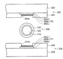
図1には予備的事項に係る電子装置に使用される導電性ボールが示されている。図1に示すように、導電性ボール100では、銅(Cu)ボール110の外面に、ニッケル(Ni)層120と錫(Sn)/銀(Ag)はんだ130とが順に形成されている。Ni層120は、Cuボール110のCuがSn/Biはんだ130に拡散することを防止するバリア層として機能する。
FIG. 1 shows a conductive ball used in an electronic device according to a preliminary matter. As shown in FIG. 1, in the
次に、図1の導電性ボール100を使用して下側配線基板と上側配線基板とを接続する方法について説明する。図2に示すように、まず、導電性ボール100の下側に配置される下側配線基板200を用意する。下側配線基板200では、絶縁層220の上に接続パッドP1が形成され、接続パッドP1の上に開口部240aが設けられたソルダレジスト層240が絶縁層220の上に形成されている。
Next, a method for connecting the lower wiring board and the upper wiring board using the
接続パッドP1は、下から順に、銅(Cu)層260a、ニッケル(Ni)層260b及び金(Au)層260cが積層されて形成される。
The connection pad P1 is formed by laminating a copper (Cu)
さらに、同じく図2に示すように、導電性ボール100の上側に配置される上側配線基板300を用意する。図2では、上側配線基板300が上下反転した状態で示されている。
Further, as shown in FIG. 2, an
上側配線基板300では、絶縁層320の上(図2では下)に接続パッドP2が形成され、接続パッドP2の上に開口部340aが設けられたソルダレジスト層340が絶縁層320の上に形成されている。接続パッドP2は、下から順に、銅(Cu)層360a、ニッケル(Ni)層360b及び金(Au)層360cが積層されて形成される。
In the
そして、図3に示すように、下側配線基板200の接続パッドP1と上側配線基板300の接続パッドP2とを図1の導電性ボール100によって接続する。
Then, as shown in FIG. 3, the connection pads P1 of the
実際には、最初に、下側配線基板200の接続パッドP1の上に導電性ボール100を配置し、リフロー加熱により、下側配線基板200の接続パッドP1に導電性ボール100のSn/Biはんだ130を接続する。
Actually, first, the
その後に、下側配線基板200に接続された導電性ボール100の上に上側配線基板300の接続パッドP2を配置する。さらに、リフロー加熱により、導電性ボール100のSn/Biはんだ130に上側配線基板300の接続パッドP2を接続する。
Thereafter, the connection pads P <b> 2 of the
このとき、リフロー加熱する際に、下側配線基板200の接続パッドP1のAu層260cが導電性ボール100のSn/Biはんだ130内に流出して消失する。また同様に、上側配線基板300の接続パッドP2のAu層360cが導電性ボール100のSn/Biはんだ130内に流出して消失する。
At this time, when reflow heating is performed, the
そして、図3の部分拡大断面図に示すように、下側配線基板200の接続パッドP1のNi層260bと導電性ボール100のSn/Biはんだ130との間にNi3Sn4層Maが形成される。Ni3Sn4層Maは、下側配線基板200の接続パッドP1のNi層260bのNiと導電性ボール100のSn/Biはんだ130のSnとが結合した金属間化合物である。
Then, as shown in the partial enlarged cross-sectional view of FIG. 3, a Ni 3 Sn 4 layer Ma is formed between the
また同様に、上側配線基板300の接続パッドP2のNi層360bと導電性ボール100のSn/Biはんだ130との間にNi3Sn4層Mbが形成される。同様に、Ni3Sn4層Mbは、上側配線基板300の接続パッドP2のNi層360bのNiと導電性ボール100のSn/Biはんだ130のSnとが結合した金属間化合物である。
Similarly, a Ni 3 Sn 4 layer Mb is formed between the
また同様に、導電性ボール100のNi層120とSn/Biはんだ130との間にNi3Sn4層Mcが形成される。Ni3Sn4層Mcは、導電性ボール100のNi層120のNiとSn/Biはんだ130のSnとが結合した金属間化合物である。
Similarly, a Ni 3 Sn 4 layer Mc is formed between the
以下、予備的事項の電子装置の課題について、下側配線基板200の接続パッドP1と導電性ボール100との接続部に注目して説明する。
Hereinafter, the subject of the electronic device as a preliminary matter will be described by paying attention to the connection portion between the connection pad P1 of the
予備的事項の電子装置で形成されるNi3Sn4層Maは熱的に不安定な物性を有する。このため、熱サイクル試験などで熱がかかると、Ni3Sn4層Maが成長するため、Ni3Sn4層Maの周りにクラックが発生しやすい。 The Ni 3 Sn 4 layer Ma formed by the preliminary electronic device has thermally unstable physical properties. For this reason, when heat is applied in a heat cycle test or the like, the Ni 3 Sn 4 layer Ma grows, so that cracks are likely to occur around the Ni 3 Sn 4 layer Ma.
また、Ni3Sn4層Maは、針状の結晶の集合体であり、各結晶の高さや幅が不均一で緻密性が低い。また、Ni3Sn4層Maは、強度が低く脆いため、ストレスがかかると折れやすい。 Further, the Ni 3 Sn 4 layer Ma is an aggregate of needle-like crystals, and the height and width of each crystal are nonuniform and the denseness is low. Further, the Ni 3 Sn 4 layer Ma has a low strength and is fragile, and therefore easily breaks when stress is applied.
このため、電流を流すとエレクトロマイグレーションによってNi3Sn4層Maの結晶の隙間から接続パッドP1のNi層260bのNiがSn/Biはんだ130に移動するため、ボイドが発生しやすい。
For this reason, when current is passed, since the Ni of the
このように、導電性ボール100の接続部に熱的に不安定な脆いNi3Sn4層Ma,Mb,Mcが形成されるため、下側配線基板200と上側配線基板300との導電性ボール100による接続の信頼性が得られない。
In this manner, thermally unstable and brittle Ni 3 Sn 4 layers Ma, Mb, and Mc are formed at the connection portion of the
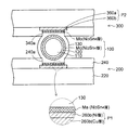
次に、下側配線基板200及び上側配線基板300の各接続パッドP1,P2がCu層から形成される場合について説明する。図4には、下側配線基板200及び上側配線基板300の各接続パッドP1,P2(Cu層)に、図1の導電性ボール100のSn/Biはんだ130がリフロー加熱によって接続された様子が示されている。
Next, a case where the connection pads P1 and P2 of the
図4の部分拡大断面図に示すように、下側配線基板200の接続パッドP1がCu層から形成される場合は、接続パッドP1と導電性ボール100のSn/Biはんだ130との間に、下から順に、Cu3Sn層Md及びCu6Sn5層Meからなる金属間化合物Mxが形成される。
As shown in the partial enlarged cross-sectional view of FIG. 4, when the connection pad P <b> 1 of the
また同様に、上側配線基板300の接続パッドP2と導電性ボール100のSn/Biはんだ130との間にも同一の金属間化合物Mxが形成される。また、導電性ボール100では、前述した図3と同様に、Ni層120とSn/Biはんだ130との間にはNi3Sn4層Mcが形成される。
Similarly, the same intermetallic compound Mx is formed between the connection pad P <b> 2 of the
接続パッドP1とSn/Biはんだ130との間にCu6Sn5層Meが形成されると、Cu6Sn5層Meは、温度変化によって違う結晶構造に変態して体積が増加するため、Cu6Sn5層Meの周りにクラックが発生する。
When the Cu 6 Sn 5 layer Me is formed between the connection pad P1 and the Sn /
このように、接続パッドP1がCu層から形成される場合は、導電性ボール100の接続部に不安定なCu6Sn5層Meが形成される。このため、下側配線基板200と上側配線基板300との導電性ボール100による接続の信頼性が得られない。
Thus, when the connection pad P <b> 1 is formed from the Cu layer, an unstable Cu 6 Sn 5 layer Me is formed at the connection portion of the
以下に説明する実施形態の導電性ボールを使用して電子装置を製造することにより、前述した課題を解消することができる。 By manufacturing an electronic device using the conductive balls of the embodiments described below, the above-described problems can be solved.
(実施の形態)
図5は実施形態の導電性ボールを示す図、図6は実施形態の導電性ボールの製造方法を示す図、図7〜図10は実施形態の電子装置を説明するための図である。
(Embodiment)
FIG. 5 is a view showing the conductive ball of the embodiment, FIG. 6 is a view showing a method of manufacturing the conductive ball of the embodiment, and FIGS. 7 to 10 are diagrams for explaining the electronic device of the embodiment.
図5に示すように、実施形態の導電性ボール1は、コアボールとして銅(Cu)ボール10を備えている。また、Cuボール10の外面の全体を被覆するニッケル(Ni)層12が形成されている。
As shown in FIG. 5, the
また、Ni層12の外面の全体を被覆する銅(Cu層)13が形成されている。さらに、Cu層13の外面の全体を被覆する錫(Sn)/ビスマス(Bi)はんだ14が形成されている。
Further, a copper (Cu layer) 13 that covers the entire outer surface of the
このように、実施形態の導電性ボール1は、Cuボール10の外面に、Ni層12、Cu層13及びSn/Biはんだ14が順に被覆されて形成される。
As described above, the
そして、実施形態の導電性ボール1では、Sn/Biはんだ14とCu層13とを合計した重量に対するCu層13の銅の重量が0.7wt%〜3wt%である。
In the
後述するように、導電性ボール1は、リフロー加熱によって電子部材の接続パッドに接続される。その際に、Cu層13のCuがSn/Biはんだ14内に拡散する。
As will be described later, the
このとき、Cu層13のCuがSn/Biはんだ14に供給されることで、Sn/Biはんだ14内のCu濃度が0.7wt%〜3wt%になるように、Cu層13の厚みが調整されている。
At this time, the thickness of the
このような条件に設定することにより、導電性ボール1のNi層12とSn/Biはんだ14との間、及び電子部材の接続パッドとSn/Biはんだ14との間に金属間化合物である(Cu,Ni)6Sn5層が形成される。
By setting such conditions, an intermetallic compound is formed between the
(Cu,Ni)6Sn5層は、前述した図4のCu6Sn5層のCuの一部がNiに置換された構造の金属間化合物である。(Cu,Ni)6Sn5層は熱的に安定な物性を有し、熱がかかっても結晶の成長が起こらない。また、(Cu,Ni)6Sn5層は、温度変化による結晶構造の変態が起こらない。さらに、(Cu,Ni)6Sn5層は、強度が強く、緻密性が高いため、信頼性の高いバリア層として機能する。 The (Cu, Ni) 6 Sn 5 layer is an intermetallic compound having a structure in which a part of Cu in the Cu 6 Sn 5 layer of FIG. 4 described above is replaced with Ni. The (Cu, Ni) 6 Sn 5 layer has thermally stable physical properties, and crystal growth does not occur even when heated. Further, in the (Cu, Ni) 6 Sn 5 layer, the crystal structure is not transformed by the temperature change. Furthermore, since the (Cu, Ni) 6 Sn 5 layer has high strength and high density, it functions as a highly reliable barrier layer.
Sn/Biはんだ14は、錫系はんだの一例であり、その他に、錫(Sn)/銀(Ag)はんだ、又は、錫(Sn)/ビスマス(Bi)/ニッケル(Ni)はんだを使用してもよい。
The Sn /
導電性ボール1はリフロー加熱する際に溶融しないCuボール10を備えているため、下側電子部材と上側電子部材とを接続する際に両者の間で一定の間隔を確保することができる。
Since the
次に、図5の実施形態の導電性ボール1の製造方法について説明する。図6(a)に示すように、まず、Cuボール10を用意する。Cuボール10の直径は、例えば130μm程度である。
Next, a method for manufacturing the
さらに、図6(b)に示すように、無電解めっきにより、Cuボール10の外面にNi層12を形成する。Ni層12を形成するための無電解めっきは、例えば、以下のような条件で行われる。
Further, as shown in FIG. 6B, the
まず、苛性ソーダ:10g/Lと界面活性剤0.5g/Lとの混合液(室温)でCuボール10を1分間処理することにより、脱脂洗浄する。続いて、Cuボール10を硫酸溶液(室温)で1分間処理することにより、酸洗浄する。
First, degreasing cleaning is performed by treating the
次いで、塩化パラジウム:2g/Lと、塩化ナトリウム:200g/Lと、35%HCl溶液:30mlとの混合液(室温)で、Cuボール10を5分間処理する。これにより、Cuボール10の外面にPdが触媒として付与される。
Next, the
その後に、硫酸ニッケル:20g/Lと次亜リン酸ナトリウム:24g/Lとを含む無電解めっき液(90℃)でCuボール10を15分間処理する。これにより、Ni層12として、厚みが2μm程度のリン(P)10wt%のNi(P)層が形成される。
Thereafter, the
次いで、図6(c)に示すように、電解めっきにより、Cuボール10を被覆するNi層12の外面にCu層13を形成する。Cu層13の電解めっきは、バレルめっきにより行われる。
Next, as shown in FIG. 6C, a
電解めっきの条件としては、硫酸銅めっき液が使用され、電流密度を1A/dm2に設定して、室温で50秒間処理する。これにより、厚みが0.11μm程度のCu層13が形成される。
As a condition for electrolytic plating, a copper sulfate plating solution is used, the current density is set to 1 A / dm 2 , and the treatment is performed at room temperature for 50 seconds. Thereby, the
さらに、図6(d)に示すように、電解めっきにより、Cuボール10を被覆するCu層13の外面にSn/Biはんだ14を形成する。Sn/Biはんだ14の電解めっきはバレルめっきによって行われる。
Further, as shown in FIG. 6D, Sn /
電解めっきの条件としては、電解Sn/Biめっき液(TB2000(石原ケミカル社製))が使用され、電流密度を2A/dm2に設定して、室温で10分間処理する。これにより、厚みが12μm程度のSn/Biはんだ14が形成される。
As electrolytic plating conditions, electrolytic Sn / Bi plating solution (TB2000 (manufactured by Ishihara Chemical Co., Ltd.)) is used, and the current density is set to 2 A / dm 2 and the treatment is performed at room temperature for 10 minutes. Thereby, the Sn /
Sn/Biはんだ14の他に、Sn/Agはんだ、又は、Sn/Bi/Niはんだを形成してもよい。
In addition to the Sn /
以上により、前述した図5の導電性ボール1が製造される。
As described above, the
次に、図7〜図10を参照して、図5の導電性ボール1を使用して電子装置を製造する方法について説明する。
Next, a method for manufacturing an electronic device using the
図7に示すように、まず、下側電子部材5を用意する。図7には、下側電子部材5の接続パッドP1の周りの様子が部分的に示されている。下側電子部材5は、例えば、配線基板又はマザーボードなどの実装基板である。
As shown in FIG. 7, first, the lower
図7に示すように、下側電子部材5では、絶縁層30の上に接続パッドP1が形成されている。また、接続パッドP1の上に開口部32xが設けられたソルダレジスト層32が絶縁層30の上に形成されている。
As shown in FIG. 7, in the lower
接続パッドP1は、下から順に、銅(Cu)層40、ニッケル(Ni)層42及び金(Au)層44が積層されて形成される。パッド状のCu層40上にソルダレジスト層32の開口部32xが配置され、Cu層40の外周部上がソルダレジスト層32で被覆されている。そして、ソルダレジスト層32の開口部32x内のCu層40の上にNi層42及Au層44がめっきによって形成される。
The connection pad P1 is formed by laminating a copper (Cu)
Cu層40は島状に配置されたパッド電極であってもよいし、あるいは、引き出し配線に繋がったパッド電極であってもよい。接続パッドP1は絶縁層30に形成されたビア導体を介して内部の配線層に接続されている。
The
そして、前述した図5の導電性ボール1を下側電子部材5の接続パッドP1の上に配置する。さらに、図8に示すように、リフロー加熱することにより、導電性ボール1のSn/Biはんだ14を溶融させて、導電性ボール1をSn/Biはんだ14によって下側電子部材5の接続パッドP1に接続する。このとき、Sn/Biはんだ14が160℃程度の温度でリフロー加熱される。
Then, the above-described
リフロー加熱により、下側電子部材5の接続パッドP1のAu層44はSn/Biはんだ14内に流出して消失する。
By reflow heating, the
そして、下側電子部材5の接続パッドP1と導電性ボール1のSn/Biはんだ14との間に、(Cu,Ni)6Sn5層M1が形成される。
Then, a (Cu, Ni) 6 Sn 5 layer M1 is formed between the connection pad P1 of the lower
リフロー加熱する際に、導電性ボール1のCu層13のCuがSn/Biはんだ14に拡散して供給される。これにより、Cuと、接続パッドP1のNi層42のNiと、Sn/Biはんだ14のSnとが結合して、(Cu,Ni)6Sn5層M1が形成される。
When reflow heating is performed, Cu in the
また、図8の部分拡大断面図に示すように、導電性ボール1のNi層12とSn/Biはんだ14との間に(Cu,Ni)6Sn5層M2が形成される。リフロー加熱する際に、導電性ボール1のCu層13のCuがSn/Biはんだ14に拡散してCu層13が消失する。
Further, as shown in the partially enlarged sectional view of FIG. 8, a (Cu, Ni) 6 Sn 5 layer M2 is formed between the
このとき、Ni層12のNiと、Sn/Biはんだ14中のCuとSnとが結合して、(Cu,Ni)6Sn5層M2が形成される。これにより、導電性ボール1のCuボール10を被覆するNi層12の外面の全体が(Cu,Ni)6Sn5層M2で被覆される。
At this time, Ni in the
次いで、図9に示すように、導電性ボール1の上側に配置される上側電子部材6を用意する。上側電子部材6は、例えば、配線基板、又は半導体チップなどの電子部品である。図9では、上側電子部材6が上下反転した状態で示されている。
Next, as shown in FIG. 9, an upper
上側電子部材6では、絶縁層30aの上(図9では下)に接続パッドP2が形成され、接続パッドP2の上に開口部32xが設けられたソルダレジスト層32aが絶縁層30aの上に形成されている。接続パッドP2は、下から順に、銅(Cu)層40a、ニッケル(Ni)層42a及び金(Au)層44aが積層されて形成される。
In the upper
そして、上側電子部材6の接続パッドP2を下側電子部材5の接続パッドP1に接続された導電性ボール1の上に配置する。
Then, the connection pad P <b> 2 of the upper
続いて、図10に示すように、リフロー加熱することにより、導電性ボール1のSn/Biはんだ14を溶融させて、上側電子部材6の接続パッドP2を導電性ボール1のSn/Biはんだ14に接続する。
Subsequently, as shown in FIG. 10, the Sn /
このとき、前述した下側電子部材5と同様に、リフロー加熱により、上側電子部材6の接続パッドP2のAu層44aはSn/Biはんだ14内に流出して消失する。
At this time, like the lower
そして、下側電子部材5と同様に、上側電子部材6の接続パッドP2のNi層42aとSn/Biはんだ14との間に(Cu,Ni)6Sn5層M3が形成される。
Similar to the lower
下側電子部材5と同様に、フロー加熱する際に、導電性ボール1のCu層13のCuがSn/Biはんだ14に拡散して供給される。これにより、Cuと、接続パッドP2のNi層42aのNiと、Sn/Biはんだ14のSnとが結合して、(Cu,Ni)6Sn5層M3が形成される。
Similar to the lower
このようにして、下側電子部材5の接続パッドP1が導電性ボール1によって上側電子部材6の接続パッドP2に接続される。導電性ボール1のCuボール10は、Sn/Biはんだ14をリフロー加熱する際に溶融しないため、下側電子部材5と上側電子部材6との間で一定の間隔を確保することができる。
In this way, the connection pad P1 of the lower
前述した形態では、下側電子部材5の第1接続パッドP1に導電性ボール1を接続した後に、導電性ボール1に上側電子部材6の接続パッドP2を接続している。これとは逆に、上側電子部材6の接続パッドP2に導電性ボール1を接続した後に、導電性ボール1に下側電子部材5の接続パッドP1を接続してもよい。
In the above-described embodiment, the
あるいは、下側電子部材5の接続パッドP1と上側電子部材6の接続パッドP2との間に導電性ボール1を配置した状態で、一括でリフロー加熱して両者を同時に接続してもよい。
Alternatively, in a state where the
このようにして、下側電子部材5の接続パッドP1と上側電子部材6の接続パッドP2とを、導電性ボール1のSn/Biはんだ14をリフロー加熱して接続する。
In this way, the connection pad P1 of the lower
以上により、図10に示すように、実施形態の電子装置2が得られる。図10に示すように、実施形態の電子装置2は下側電子部材5を備えている。下側電子部材5では、絶縁層30の上に接続パッドP1が形成されている。さらに、接続パッドP1の上に開口部32xが設けられたソルダレジスト層32が絶縁層30の上に形成されている。
As described above, as shown in FIG. 10, the
接続パッドP1は、Cu層40とその上に配置されたNi層42とにより形成される。接続パッドP1の表面がNi層42から形成されている。
The connection pad P1 is formed by the
ソルダレジスト層32の開口部32xがパッド状のCu層40上に配置され、Cu層40の外周部上がソルダレジスト層32で被覆されている。そして、ソルダレジスト層32の開口部32x内のCu層40の上にNi層42が形成されている。
An
また、下側電子部材5の接続パッドP1に導電性ボール1が接続されている。導電性ボール1は、Cuボール10と、Cuボール10の外面を被覆するNi層12と、Ni層12の外面を被覆するSn/Biはんだ14とを有する。
In addition, the
そして、下側電子部材5の接続パッドP1のNi層42と、導電性ボール1のSn/Biはんだ14との間に(Cu,Ni)6Sn5層M1が形成されている。前述したように、(Cu,Ni)6Sn5層M1は、導電性ボール1のCu層13から供給されたCuと、接続パッドP1のNi層42のNiと、Sn/Biはんだ14のSnとが結合した金属間化合物である。
A (Cu, Ni) 6 Sn 5 layer M 1 is formed between the
また、実施形態の電子装置2は下側電子部材5の上に配置された上側電子部材6を備えている。下側電子部材5の接続パッドP1と上側電子部材6の接続パッドP2との間に導電性ボール1が配置され、接続パッドP1と第2接続パッドP2とが導電性ボール1によって接続されている。
Further, the
このようにして、下側電子部材5が導電性ボール1によって上側電子部材6に接続されている。上側電子部材6は上下反転した状態となっている。
In this way, the lower
上側電子部材6では、絶縁層30aの上(図10では下)に接続パッドP2が形成されている。さらに、接続パッドP2の上に開口部32xが設けられたソルダレジスト層32aが絶縁層30aの上に形成されている。
In the upper
下側電子部材5と同様に、接続パッドP2は、Cu層40aとその上に配置されたNi層42aとにより形成される。ソルダレジスト層32aの開口部32xがパッド状のCu層40a上に配置され、Cu層40aの外周部上がソルダレジスト層32aで被覆されている。ソルダレジスト層32aの開口部32x内のCu層40aの上にNi層42aが形成されている。
Similar to the lower
また、下側電子部材5と同様に、上側電子部材6の接続パッドP2のNi層42aと、導電性ボール1のSn/Biはんだ14との間に(Cu,Ni)6Sn5層M3が形成されている。下側電子部材5と同様に、(Cu,Ni)6Sn5層M3は、導電性ボール1のCu層13から供給されたCuと、接続パッドP2のNi層42aのNiと、Sn/Biはんだ14のSnとが結合した金属間化合物である。
Similarly to the lower
このように、本実施形態の電子装置2では、下側電子部材5の接続パッドP1のNi層42と導電性ボール1のSn/Biはんだ14との間に、金属間化合物である(Cu,Ni)6Sn5層M1が形成されている。
As described above, in the
(Cu,Ni)6Sn5層M1は、予備的事項で説明したNi3Sn4層Maと違って、熱的に安定な物性を有する。このため、熱サイクル試験などで熱がかかっても、結晶の成長が起こらない。また、(Cu,Ni)6Sn5層M1は、予備的事項で説明したCu6Sn5層Meと違って、温度変化による結晶構造の変態が起こらない。このため、(Cu,Ni)6Sn5層M1の周囲にクラックが発生することが防止される。 The (Cu, Ni) 6 Sn 5 layer M1 has thermally stable physical properties, unlike the Ni 3 Sn 4 layer Ma described in the preliminary matter. For this reason, crystal growth does not occur even when heat is applied in a thermal cycle test or the like. In addition, unlike the Cu 6 Sn 5 layer Me described in the preliminary matter, the (Cu, Ni) 6 Sn 5 layer M1 does not undergo a transformation of the crystal structure due to a temperature change. For this reason, the occurrence of cracks around the (Cu, Ni) 6 Sn 5 layer M1 is prevented.
さらに、(Cu,Ni)6Sn5層M1は、予備的事項で説明したNi3Sn4層Maと違って、ドーム状の結晶の集合体であり、各結晶の高さや幅が均一で緻密性が高い。また、(Cu,Ni)6Sn5層M1は、強度が強く、ストレスがかかっても折れにくい。 Further, unlike the Ni 3 Sn 4 layer Ma described in the preliminary matter, the (Cu, Ni) 6 Sn 5 layer M1 is an aggregate of dome-shaped crystals, and the height and width of each crystal is uniform and dense. High nature. Further, the (Cu, Ni) 6 Sn 5 layer M1 has high strength and is not easily broken even when stress is applied.
このため、(Cu,Ni)6Sn5層M1が信頼性の高いバリア層として機能する。これにより、下側電子部材5の接続パッドP1のNi層40のNiがエレクトロマイグレーションによって移動することが抑止され、導電性ボール1の接続部にボイドが発生することが防止される。
For this reason, the (Cu, Ni) 6 Sn 5 layer M1 functions as a highly reliable barrier layer. Thereby, it is suppressed that Ni of the
また、上側電子部材6の接続パッドP2のNi層42aと導電性ボール1のSn/Biはんだ14との間に、同様に、(Cu,Ni)6Sn5層M3が形成されている。このため、同様な理由により、上側電子部材6の接続パッドP2と導電性ボール1との接続の信頼性を向上させることができる。
Similarly, a (Cu, Ni) 6 Sn 5 layer M3 is formed between the
さらに、図10の部分拡大断面図を参照すると、導電性ボール1のNi層12とSn/Biはんだ14との間に(Cu,Ni)6Sn5層M2が形成されている。前述したように、(Cu,Ni)6Sn5層M2は、Cu層13から供給されたCuと、Ni層12のNiと、Sn/Biはんだ14のSnとが結合した金属間化合物である。
Furthermore, referring to the partially enlarged sectional view of FIG. 10, a (Cu, Ni) 6 Sn 5 layer M2 is formed between the
このように、導電性ボール1のCuボール10を覆うNi層12の外面の全体に(Cu,Ni)6Sn5層M2が形成されている。
Thus, the (Cu, Ni) 6 Sn 5 layer M2 is formed on the entire outer surface of the
導電性ボール1に形成される(Cu,Ni)6Sn5層M2においても、前述したように、結晶の成長や変態が起こらないため、導電性ボール1による接続部にクラックが発生することが防止される。
Even in the (Cu, Ni) 6 Sn 5 layer M2 formed on the
また、エレクトロマイグレーションによって導電性ボール1のNi層12のNiが移動することが抑止され、導電性ボール1による接続部にボイドが発生することが防止される。
In addition, the migration of Ni in the
なお、図10において、導電性ボール1に形成された(Cu,Ni)6Sn5層M2と接続パッドP1に形成された(Cu,Ni)6Sn5層M1とが接して形成されてもよい。また、導電性ボール1に形成された(Cu,Ni)6Sn5層M2と接続パッドP2に形成された(Cu,Ni)6Sn5層M2とが接して形成されてもよい。
In FIG. 10, even if the (Cu, Ni) 6 Sn 5 layer M2 formed on the
ここで、下側電子部材5及び上側電子部材6の接続パッドP1,P2の各Ni層42,42a及び導電性ボール1のNi層12の上に、(Cu,Ni)6Sn5層M1〜M3が形成される条件について説明する。
Here, the (Cu, Ni) 6 Sn 5 layer M1 is formed on the Ni layers 42 and 42a of the connection pads P1 and P2 of the lower
導電性ボール1をリフロー加熱して接続する際に、導電性ボール1のCu層13のCuがSn/Biはんだ14に拡散する。このとき、Sn/Biはんだ14中のCu濃度が0.7wt%〜3wt%の範囲になるように調整することにより、(Cu,Ni)6Sn5層M1〜M3が形成される。
When the
本願発明者は、上記した条件で実際に(Cu,Ni)6Sn5層が形成されるかどうか確認実験を行った。 The inventor of the present application conducted an experiment to confirm whether or not the (Cu, Ni) 6 Sn 5 layer is actually formed under the above-described conditions.
図11に示すように、実験サンプルとして、下側基板5a及び上側基板6aを用意した。下側基板5aでは、絶縁層30bの上にパッド状のCu層40bが形成され、Cu層40bの上に開口部32xが設けられたソルダレジスト層32bが形成されている。
As shown in FIG. 11, a
さらに、ソルダレジスト層32の開口部32x内のCu層40bの上にNi層42b、Pd層43b及びAu層44bが形成されている。Cu層40b、Ni層42b、Pd層43b及びAu層44bにより接続パッドPxが形成される。また、上側基板6aでは、絶縁層30cにCuピラー48が形成されている。
Further, a
次いで、96wt%Sn/3.5wt%Ag/0.5wt%Cuのはんだペースト49aを下側基板5aの接続パッドPxの上に塗布した。
Next, a
本実験サンプルは、前述した図10の接続構造の疑似実験であり、上側基板6aのCuピラー48が導電性ボール1のCu層13(図5)に相当し、はんだペースト49aが導電性ボール1のSn/Biはんだ14に相当する。
This experimental sample is a pseudo experiment of the connection structure of FIG. 10 described above. The
そして、図12に示すように、上側基板6aのCuピラー48を下側基板5aの接続パッドPx上のはんだペースト49aに配置し、リフロー加熱を行った。これにより、上側基板6aのCuピラー48をはんだ49によって下側基板5aの接続パッドPxに接続した。
Then, as shown in FIG. 12, the
このとき、接続パッドPxのAu層44b及びPd層43bははんだペースト49a内に流出して消失する。さらに、Cuピラー48のCuがはんだペースト49aに拡散し、はんだペースト49a内のCu濃度が0.5wt%から0.7wt%に増加する。
At this time, the
これにより、下側基板5aの接続パッドPxのNi層42bとはんだ49との間に(Cu,Ni)6Sn5層M1が形成された。
Thus, a (Cu, Ni) 6 Sn 5 layer M1 was formed between the
本願発明者は、図12のM1で示された層をEDX(エネルギー分散型X線分析)により分析することにより、M1で示された層は(Cu,Ni)6Sn5層であることが確認された。 The inventor of the present application analyzes the layer indicated by M1 in FIG. 12 by EDX (energy dispersive X-ray analysis), so that the layer indicated by M1 is a (Cu, Ni) 6 Sn 5 layer. confirmed.
このように、導電性ボール1のCu層13からのCuの拡散によって、Sn/Biはんだ14中のCu濃度が0.7wt%〜3wt%の範囲内になるように調整することにより、(Cu,Ni)6Sn5層が形成されることが確認された。
Thus, by adjusting the Cu concentration in the Sn /
図13には、前述した図5の導電性ボール1のCu層13の厚み(μm)に対するSn/Biはんだ14中のCu濃度(wt%)の関係が示されている。
FIG. 13 shows the relationship of the Cu concentration (wt%) in the Sn /
例えば、図13に示す導電性ボール1のように、Cuボール10の直径を130μmとし、Ni層12の厚みを2μmとし、Sn/Biはんだ14の厚みを13μmとする。
For example, like the
この場合、図13のグラフに示すように、図13に示す導電性ボール1のCu層13の厚みが0.11μm程度であれば、Sn/Biはんだ14中のCu濃度が0.7wt%になる。このとき、Cu層13のCuがSn/Biはんだ14に拡散してCu層13が消失する。
In this case, as shown in the graph of FIG. 13, if the thickness of the
この例のように、リフロー加熱される際に、Sn/Biはんだ14中のCu濃度が0.7wt%〜3wt%の範囲になるように、Cuボール10の直径、Ni層12及びSn/Biはんだ14の各厚みに応じて、Cu層13の厚みを調整すればよい。
As in this example, when reflow heating is performed, the diameter of the
次に、実施形態の変形例の電子装置について説明する。図14は実施形態の変形例の電子装置を示す図である。図14に示すように、変形例の電子装置2aでは、下側電子部材5及び上側電子部材6の各接続パッドP1,P2は、Ni層及びAu層が省略され、Cu層から形成される。
Next, an electronic device according to a modification of the embodiment will be described. FIG. 14 is a diagram illustrating an electronic device according to a modification of the embodiment. As shown in FIG. 14, in the
図14には、下側電子部材5及び上側電子部材6の各接続パッドP1,P2(Cu層)に、図5の導電性ボール1のSn/Biはんだ14がリフロー加熱によって接続された様子が示されている。
FIG. 14 shows that the Sn /
図14に示すように、変形例の電子装置2aでは、下側電子部材5の接続パッドP1(Cu層)と導電性ボール1のSn/Biはんだ14との間に、下から順に、Cu3Sn層My及び(Cu,Ni)6Sn5層M4が形成される。下側電子部材5の接続パッドP1(Cu層)のCuと、Sn/Biはんだ14のSnとが結合して、接続パッドP1の上にCu3Sn層Myが形成される。
As shown in FIG. 14, in the
また、導電性ボール1のCu層13のCuとNi層12のNiとがSn/Biはんだ14に拡散することで、CuとNiとSnとが結合して接続パッドP1上のCu3Sn層Myの上に(Cu,Ni)6Sn5層M4が形成される。Niは、Cu層13のCuが全てSn/Biはんだ14に拡散した後に、露出したNi層12から供給される。
Further, Cu in the
また同様に、上側電子部材6の接続パッドP2(Cu層)と導電性ボール1のSn/Biはんだ14との間に、下から順に、Cu3Sn層My及び(Cu,Ni)6Sn5層M5が形成される。
Similarly, between the connection pad P2 (Cu layer) of the upper
上側電子部材6の接続パッドP2(Cu層)のCuと、導電性ボール1のSn/Biはんだ14のSnとが結合して、接続パッドP2の上にCu3Sn層Myが形成される。
Cu of the connection pad P2 (Cu layer) of the upper
また、導電性ボール1のCu層13のCuとNi層12のNiとがSn/Biはんだ14に拡散することで、CuとNiとSnとが結合して接続パッドP2上のCu3Sn層Myの上に(Cu,Ni)6Sn5層M5が形成される。
Also, Cu in the
また、導電性ボール1では、前述した図10と同様に、Ni層12とSn/Biはんだ14との間に(Cu,Ni)6Sn5層M2が形成される。
Further, in the
図14において、下側電子部材5及び上側電子部材6の各接続パッドP1,P2(Cu層)上に、Cu3Sn層My及び(Cu,Ni)6Sn5層M4,M5が形成されること以外は、前述した図10と同一である。このため、図14のその他の要素には図10と同一符号を付してその詳しい説明を省略する。
In FIG. 14, Cu 3 Sn layer My and (Cu, Ni) 6 Sn 5 layers M4 and M5 are formed on connection pads P1 and P2 (Cu layers) of lower
変形例の電子装置2aでは、下側電子部材5及び上側電子部材6の各接続パッドP1,P2がNi層を備えていないため、導電性ボール1のNi層12からNiが供給されて(Cu,Ni)6Sn5層M4,M5が形成される。
In the
このとき、導電性ボール1の銅層13のCuが全て拡散した後に、Ni層12からNiが供給される。このため、Niが十分に供給されるように、銅層13は最低限の厚みに設定され、リフロー加熱の処理時間や温度が最適に調整される。
At this time, Ni is supplied from the
変形例の電子装置2aでは、図10の電子装置2と同様に、接続パッドP1,P2(Cu層)とSn/Biはんだ14との間、及び導電性ボール1のNi層12とSn/Biはんだ14との間に熱的に安定な(Cu,Ni)6Sn5層M4,M5,M2が形成されている。
In the
このため、下側電子部材5と上側電子部材6との導電性ボール1による接続の信頼性を向上させることができる。
For this reason, the reliability of the connection by the
前述した図10及び図14において、導電性ボール1のSn/Biはんだ14の代わりに、Sn/Agはんだ、又は、Sn/Bi/Niはんだを使用する場合も同様な金属間化合物が形成される。
10 and 14, the same intermetallic compound is formed when Sn / Ag solder or Sn / Bi / Ni solder is used instead of the Sn /
なお、図14において、導電性ボール1に形成された(Cu,Ni)6Sn5層M2と接続パッドP1に形成された(Cu,Ni)6Sn5層M4とが接して形成されてもよい。また、導電性ボール1に形成された(Cu,Ni)6Sn5層M2と接続パッドP2に形成された(Cu,Ni)6Sn5層M5とが接して形成されてもよい。
In FIG. 14, the (Cu, Ni) 6 Sn 5 layer M2 formed on the
次に、前述した図15の導電性ボールによる接続構造を適用した実施形態の電子装置について説明する。 Next, an electronic device according to an embodiment to which the above-described connection structure using conductive balls in FIG. 15 is applied will be described.
図15には、実施形態の第1の適用例の電子装置が示されている。図15に示すように、実施形態の第1の適用例の電子装置3では、下側にマザーボードなどの実装基板50を備えている。
FIG. 15 illustrates an electronic apparatus according to a first application example of the embodiment. As shown in FIG. 15, the electronic device 3 according to the first application example of the embodiment includes a mounting
実装基板50では、上面側に接続パッドP1が形成され、下面側に配線層52が形成されている。下面側の配線層52は絶縁層54で被覆されている。また、実装基板50には、上面側の接続パッドP1上に開口部56aが設けられた絶縁層56が形成されている。実装基板50は、下側電子部材の一例である。
In the mounting
そして、実装基板50の上面側の接続パッドP1に導電性ボール1のSn/Biはんだ14が接続されている。
The Sn /
さらに、実装基板50の上に導電性ボール1を介して配線基板60が配置されている。配線基板60では、両面側に接続パッドP2が形成され、両面側の接続パッドP2が貫通導体62を介して相互接続されている。
Further, the
配線基板60には、両面側の接続パッドP2上に開口部64aが設けられたソルダレジスト層64がそれぞれ形成されている。配線基板60は上側電子部材又は下側電子部材の一例である。
On the
そして、配線基板60の下面側の接続パッドP2が導電性ボール1のSn/Biはんだ14に接続されている。
The connection pad P2 on the lower surface side of the
実装基板50の接続パッドP1と配線基板60の下面側の接続パッドP2とが導電性ボール1で接続される構造に、前述した図10又は図14の導電性ボール1による接続構造が適用される。
The connection structure using the
さらに、配線基板60の上面側の接続パッドP2に導電性ボール1のSn/Biはんだ14が接続されている。また、半導体チップ70の接続パッドP3が配線基板60に接続された導電性ボール1のSn/Biはんだ14に接続されている。また、半導体チップ70の下側にアンダーフィル樹脂72が充填されている。半導体チップ70は上側電子部材の一例である。
Further, the Sn /
配線基板60の接続パッドP2と半導体チップ70の接続パッドP3とが導電性ボール1で接続される構造に、前述した図10又は図14の導電性ボール1による接続構造が適用される。
The connection structure using the
図16には、実施形態の第2の適用例の電子装置が示されている。図16に示すように、実施形態の第2の適用例の電子装置3aでは、下側に図15の配線基板60と同一構造の下側配線基板60aが配置されている。
FIG. 16 shows an electronic apparatus according to a second application example of the embodiment. As shown in FIG. 16, in the
そして、下側配線基板60aの上面側の接続パッドP2に半導体チップ70がはんだバンプ74によってフリップチップ接続されている。半導体チップ70の下面側にアンダーフィル樹脂72が充填されている。下側配線基板60aは下側電子部材の一例である。
The
さらに、下側配線基板60aの上面側の接続パッドP2に導電性ボール1のSn/Biはんだ14が接続されている。
Furthermore, the Sn /
また、下側配線基板60aの上に導電性ボール1を介して上側配線基板80が配置されている。上側配線基板80では、両面側に接続パッドP4が形成され、両面側の接続パッドP4が貫通導体82を介して相互接続されている。
Further, the
上側配線基板80には、両面側の接続パッドP4上に開口部84aが設けられたソルダレジスト層84がそれぞれ形成されている。
On the
そして、上側配線基板80の下面側の接続パッドP4が導電性ボール1のSn/Biはんだ14に接続されている。上側配線基板80は上側電子部材の一例である。さらに、下側配線基板60aと上側配線基板80との間に封止樹脂90が充填されている。封止樹脂90によって、半導体チップ70と導電性ボール1とが封止されている。
The connection pad P4 on the lower surface side of the
下側配線基板60aの上面側の接続パッドP2と上側配線基板80の下面側の接続パッドP4とが導電性ボール1で接続される構造に、前述した図10又は図14の導電性ボール1による接続構造が適用される。
In the structure in which the connection pad P2 on the upper surface side of the
1…導電性ボール、2,2a,3,3a…電子装置、5…下側電子部材、6…上側電子部材、10…Cuボール、12,42,42a…Ni層、13…Cu層、14…Sn/Biはんだ、30,30a,54,56…絶縁層、32,32a,64,84…ソルダレジスト層、40,40a…Cu層、44,44a…Au層、50…実装基板、52…配線層、60…配線基板、60a…下側配線基板、62,82…貫通導体、70…半導体チップ、72…アンダーフィル樹脂、74…はんだバンプ、80…上側配線基板、90…封止樹脂、M1,M2,M3,M4,M5…(Cu,Ni)6Sn5層、My…Cu3Sn層、P1,P2,P3,P4…接続パッド。
DESCRIPTION OF
Claims (11)
前記銅ボールの外面を被覆するニッケル層と、
前記ニッケル層の外面を被覆する銅層と、
前記銅層の外面を被覆する錫系はんだと
を有し、
前記錫系はんだと前記銅層とを合計した重量に対する前記銅層の銅の重量が0.7wt%〜3wt%であることを特徴とする導電性ボール。 Copper balls,
A nickel layer covering the outer surface of the copper ball;
A copper layer covering the outer surface of the nickel layer;
A tin-based solder covering the outer surface of the copper layer,
The conductive ball, wherein a weight of copper in the copper layer is 0.7 wt% to 3 wt% with respect to a total weight of the tin-based solder and the copper layer.
前記下側電子部材の上に配置され、第2接続パッドを備えた上側電子部材と、
前記下側電子部材の第1接続パッドと前記上側電子部材の第2接続パッドとを接続する導電性ボールと
を有し、
前記導電性ボールは、
銅ボールと、
前記銅ボールの外面を被覆するニッケル層と、
前記銅層の外面を被覆する錫系はんだと
を有し、
前記ニッケル層と前記錫系はんだとの間に(Cu,Ni)6Sn5層が形成されていることを特徴とする電子装置。 A lower electronic member having a first connection pad;
An upper electronic member disposed on the lower electronic member and provided with a second connection pad;
A conductive ball connecting the first connection pad of the lower electronic member and the second connection pad of the upper electronic member;
The conductive ball is
Copper balls,
A nickel layer covering the outer surface of the copper ball;
A tin-based solder covering the outer surface of the copper layer,
An electronic device, wherein a (Cu, Ni) 6 Sn 5 layer is formed between the nickel layer and the tin-based solder.
前記第1接続パッドと前記錫系はんだとの間、及び前記第2接続パッドと前記錫系はんだとの間に、(Cu,Ni)6Sn5層がそれぞれ形成されていることを特徴とする請求項4に記載の電子装置。 Each surface of the first connection pad and the second connection pad is a nickel layer or a copper layer,
A (Cu, Ni) 6 Sn 5 layer is formed between the first connection pad and the tin-based solder and between the second connection pad and the tin-based solder, respectively. The electronic device according to claim 4.
前記銅ボールの外面を被覆するニッケル層を形成する工程と、
前記ニッケル層の外面を被覆する銅層を形成する工程と、
前記銅層の外面を被覆する錫系はんだを形成する工程と
を有し、
前記錫系はんだがリフロー加熱される際に、前記銅層の銅が前記錫系はんだに拡散して、前記錫系はんだ内の銅の濃度が0.7wt%〜3wt%になるように、前記銅層の厚みが調整されることを特徴とする導電性ボールの製造方法。 Preparing a copper ball;
Forming a nickel layer covering the outer surface of the copper ball;
Forming a copper layer covering the outer surface of the nickel layer;
Forming a tin-based solder covering the outer surface of the copper layer,
When the tin-based solder is reflow-heated, the copper of the copper layer diffuses into the tin-based solder, so that the concentration of copper in the tin-based solder is 0.7 wt% to 3 wt%. A method for producing a conductive ball, wherein the thickness of the copper layer is adjusted.
第2接続パッドを備えた上側電子部材と、
銅ボールと、前記銅ボールの外面を被覆するニッケル層と、前記ニッケル層の外面を被覆する銅層と、前記銅層の外面を被覆する錫系はんだとを有する導電性ボールと
を用意する工程と、
前記下側電子部材の第1接続パッドと前記上側電子部材の第2接続パッドとを、前記導電性ボールの錫系はんだをリフロー加熱して接続する工程と
を有し、
前記導電性ボールの前記ニッケル層と前記錫系はんだとの間に(Cu,Ni)6Sn5層が形成されることを特徴とする電子装置の製造方法。 A lower electronic member having a first connection pad;
An upper electronic member having a second connection pad;
Preparing a copper ball, a nickel layer covering the outer surface of the copper ball, a copper layer covering the outer surface of the nickel layer, and a tin-based solder covering the outer surface of the copper layer When,
Connecting the first connection pad of the lower electronic member and the second connection pad of the upper electronic member by reflow heating the tin-based solder of the conductive ball,
A method of manufacturing an electronic device, wherein a (Cu, Ni) 6 Sn 5 layer is formed between the nickel layer of the conductive ball and the tin-based solder.
前記錫系はんだをリフロー加熱する際に、前記銅層の銅が前記錫系はんだに拡散して、前記錫系はんだ内の銅の濃度が0.7wt%〜3wt%になるように、前記銅層の厚みが調整されていることを特徴とする請求項8に記載の電子装置の製造方法。 In the step of preparing the conductive ball,
When reflow heating the tin-based solder, the copper in the copper layer diffuses into the tin-based solder, so that the copper concentration in the tin-based solder is 0.7 wt% to 3 wt%. The method of manufacturing an electronic device according to claim 8, wherein the thickness of the layer is adjusted.
前記第1接続パッド及び前記第2接続パッドの各表面はニッケル層又は銅層であり、
前記第1接続パッドと前記錫系はんだとの間、及び前記第2接続パッドと前記錫系はんだとの間に、(Cu,Ni)6Sn5層がそれぞれ形成されることを特徴とする請求項8又は9に記載の電子装置の製造方法。 In the step of connecting the first connection pad of the lower electronic member and the second connection pad of the upper electronic member,
Each surface of the first connection pad and the second connection pad is a nickel layer or a copper layer,
The (Cu, Ni) 6 Sn 5 layer is formed between the first connection pad and the tin-based solder, and between the second connection pad and the tin-based solder, respectively. Item 10. A method for manufacturing an electronic device according to Item 8 or 9.
Priority Applications (2)
| Application Number | Priority Date | Filing Date | Title |
|---|---|---|---|
| JP2017133267A JP7014535B2 (en) | 2017-07-07 | 2017-07-07 | Conductive balls and electronic devices and their manufacturing methods |
| US16/023,500 US10446513B2 (en) | 2017-07-07 | 2018-06-29 | Conductive ball having a tin-based solder covering an outer surface of the copper ball |
Applications Claiming Priority (1)
| Application Number | Priority Date | Filing Date | Title |
|---|---|---|---|
| JP2017133267A JP7014535B2 (en) | 2017-07-07 | 2017-07-07 | Conductive balls and electronic devices and their manufacturing methods |
Publications (3)
| Publication Number | Publication Date |
|---|---|
| JP2019013960A true JP2019013960A (en) | 2019-01-31 |
| JP2019013960A5 JP2019013960A5 (en) | 2020-04-09 |
| JP7014535B2 JP7014535B2 (en) | 2022-02-01 |
Family
ID=64903406
Family Applications (1)
| Application Number | Title | Priority Date | Filing Date |
|---|---|---|---|
| JP2017133267A Active JP7014535B2 (en) | 2017-07-07 | 2017-07-07 | Conductive balls and electronic devices and their manufacturing methods |
Country Status (2)
| Country | Link |
|---|---|
| US (1) | US10446513B2 (en) |
| JP (1) | JP7014535B2 (en) |
Cited By (1)
| Publication number | Priority date | Publication date | Assignee | Title |
|---|---|---|---|---|
| WO2024038665A1 (en) * | 2022-08-16 | 2024-02-22 | 日立Astemo株式会社 | Electronic device and method for manufacturing electronic device |
Families Citing this family (3)
| Publication number | Priority date | Publication date | Assignee | Title |
|---|---|---|---|---|
| JP7041477B2 (en) * | 2017-07-05 | 2022-03-24 | 新光電気工業株式会社 | Conductive balls and electronic devices and their manufacturing methods |
| US11145614B2 (en) * | 2019-10-18 | 2021-10-12 | Taiwan Semiconductor Manufacturing Company, Ltd. | Semiconductor device and method of manufacture |
| KR102461313B1 (en) * | 2020-05-19 | 2022-11-01 | 엠케이전자 주식회사 | Semiconductor package using core for reverse reflow |
Citations (5)
| Publication number | Priority date | Publication date | Assignee | Title |
|---|---|---|---|---|
| JP2007075856A (en) * | 2005-09-14 | 2007-03-29 | Nippon Steel Materials Co Ltd | Cu CORE BALL |
| JP2010099736A (en) * | 2008-09-25 | 2010-05-06 | Hitachi Metals Ltd | Connection terminal ball having excellent drop impact resistance characteristic, connection terminal, and electronic component |
| JP2013031864A (en) * | 2011-08-01 | 2013-02-14 | Hitachi Metals Ltd | Solder ball and semiconductor device using solder ball |
| JP2015186826A (en) * | 2015-06-05 | 2015-10-29 | 日立金属株式会社 | Solder ball and semiconductor device |
| JP2016106033A (en) * | 2007-10-19 | 2016-06-16 | 株式会社日本スペリア社 | Solder joint |
Family Cites Families (2)
| Publication number | Priority date | Publication date | Assignee | Title |
|---|---|---|---|---|
| JP2015072996A (en) | 2013-10-02 | 2015-04-16 | 新光電気工業株式会社 | Semiconductor device |
| TWI637465B (en) * | 2017-06-03 | 2018-10-01 | 矽品精密工業股份有限公司 | Electronic package and the manufacture thereof |
-
2017
- 2017-07-07 JP JP2017133267A patent/JP7014535B2/en active Active
-
2018
- 2018-06-29 US US16/023,500 patent/US10446513B2/en active Active
Patent Citations (5)
| Publication number | Priority date | Publication date | Assignee | Title |
|---|---|---|---|---|
| JP2007075856A (en) * | 2005-09-14 | 2007-03-29 | Nippon Steel Materials Co Ltd | Cu CORE BALL |
| JP2016106033A (en) * | 2007-10-19 | 2016-06-16 | 株式会社日本スペリア社 | Solder joint |
| JP2010099736A (en) * | 2008-09-25 | 2010-05-06 | Hitachi Metals Ltd | Connection terminal ball having excellent drop impact resistance characteristic, connection terminal, and electronic component |
| JP2013031864A (en) * | 2011-08-01 | 2013-02-14 | Hitachi Metals Ltd | Solder ball and semiconductor device using solder ball |
| JP2015186826A (en) * | 2015-06-05 | 2015-10-29 | 日立金属株式会社 | Solder ball and semiconductor device |
Cited By (1)
| Publication number | Priority date | Publication date | Assignee | Title |
|---|---|---|---|---|
| WO2024038665A1 (en) * | 2022-08-16 | 2024-02-22 | 日立Astemo株式会社 | Electronic device and method for manufacturing electronic device |
Also Published As
| Publication number | Publication date |
|---|---|
| JP7014535B2 (en) | 2022-02-01 |
| US20190013286A1 (en) | 2019-01-10 |
| US10446513B2 (en) | 2019-10-15 |
Similar Documents
| Publication | Publication Date | Title |
|---|---|---|
| JP7014535B2 (en) | Conductive balls and electronic devices and their manufacturing methods | |
| TWI353643B (en) | Dual metal stud bumping for flip chip applications | |
| JP6667765B2 (en) | Electrode connection method and electrode connection structure | |
| JP3829325B2 (en) | Semiconductor element, manufacturing method thereof, and manufacturing method of semiconductor device | |
| TWI452657B (en) | Soldering method and related device for improved resistance to brittle fracture | |
| TWI390642B (en) | Stable gold bump solder connections | |
| TWI571191B (en) | Electrolytic deposition and via filling in coreless substrate processing | |
| JP7041477B2 (en) | Conductive balls and electronic devices and their manufacturing methods | |
| US9129884B2 (en) | Solder bump joining structure with low resistance joining member | |
| US20100105173A1 (en) | Method of producing semiconductor device provided with flip-chip mounted semiconductor element | |
| TWI493672B (en) | Semiconductor device, electronic device, and semiconductor device manufacturing method | |
| US20060267157A1 (en) | Solder joints for copper metallization having reduced interfacial voids | |
| JP2014116367A (en) | Electronic component, method of manufacturing electronic device and electronic device | |
| JP2009239278A (en) | Substrate for mounting electronic component, and method of manufacturing the same | |
| TW201505492A (en) | Printed circuit board and manufacturing method thereof | |
| TWI473221B (en) | Package substrate and fabrication method thereof | |
| TW545098B (en) | Fine pad pitch organic circuit board with plating solder and method for fabricating the same | |
| JP2008028069A (en) | Substrate with externally bonded electrode, and method for manufacturing the same | |
| JP2003133474A (en) | Mounting structure of electronic device | |
| JPH02276249A (en) | Manufacture of semiconductor circuit bump | |
| TWI313911B (en) | Conductive structure of package substrate and manufacturing method thereof | |
| JP4562314B2 (en) | Electronic device mounting structure | |
| JPH10335388A (en) | Ball grid array | |
| JP2002261115A (en) | Structure for mounting electronic apparatus | |
| JP2002353368A (en) | Mounting structure of electronic apparatus |
Legal Events
| Date | Code | Title | Description |
|---|---|---|---|
| RD03 | Notification of appointment of power of attorney |
Free format text: JAPANESE INTERMEDIATE CODE: A7423 Effective date: 20180320 |
|
| A521 | Request for written amendment filed |
Free format text: JAPANESE INTERMEDIATE CODE: A523 Effective date: 20200227 |
|
| A621 | Written request for application examination |
Free format text: JAPANESE INTERMEDIATE CODE: A621 Effective date: 20200227 |
|
| A977 | Report on retrieval |
Free format text: JAPANESE INTERMEDIATE CODE: A971007 Effective date: 20210224 |
|
| A131 | Notification of reasons for refusal |
Free format text: JAPANESE INTERMEDIATE CODE: A131 Effective date: 20210309 |
|
| A521 | Request for written amendment filed |
Free format text: JAPANESE INTERMEDIATE CODE: A523 Effective date: 20210427 |
|
| A131 | Notification of reasons for refusal |
Free format text: JAPANESE INTERMEDIATE CODE: A131 Effective date: 20210803 |
|
| A521 | Request for written amendment filed |
Free format text: JAPANESE INTERMEDIATE CODE: A523 Effective date: 20210906 |
|
| TRDD | Decision of grant or rejection written | ||
| A01 | Written decision to grant a patent or to grant a registration (utility model) |
Free format text: JAPANESE INTERMEDIATE CODE: A01 Effective date: 20220111 |
|
| A61 | First payment of annual fees (during grant procedure) |
Free format text: JAPANESE INTERMEDIATE CODE: A61 Effective date: 20220120 |