JP2018531514A - Group III nitride semiconductor light emitting device having amber to red emission (> 600 nm) and method for making the same - Google Patents
Group III nitride semiconductor light emitting device having amber to red emission (> 600 nm) and method for making the same Download PDFInfo
- Publication number
- JP2018531514A JP2018531514A JP2018517812A JP2018517812A JP2018531514A JP 2018531514 A JP2018531514 A JP 2018531514A JP 2018517812 A JP2018517812 A JP 2018517812A JP 2018517812 A JP2018517812 A JP 2018517812A JP 2018531514 A JP2018531514 A JP 2018531514A
- Authority
- JP
- Japan
- Prior art keywords
- multiple quantum
- quantum well
- layer
- nitride semiconductor
- indium concentration
- Prior art date
- Legal status (The legal status is an assumption and is not a legal conclusion. Google has not performed a legal analysis and makes no representation as to the accuracy of the status listed.)
- Pending
Links
Images


Classifications
-
- H—ELECTRICITY
- H01—ELECTRIC ELEMENTS
- H01L—SEMICONDUCTOR DEVICES NOT COVERED BY CLASS H10
- H01L33/00—Semiconductor devices with at least one potential-jump barrier or surface barrier specially adapted for light emission; Processes or apparatus specially adapted for the manufacture or treatment thereof or of parts thereof; Details thereof
- H01L33/02—Semiconductor devices with at least one potential-jump barrier or surface barrier specially adapted for light emission; Processes or apparatus specially adapted for the manufacture or treatment thereof or of parts thereof; Details thereof characterised by the semiconductor bodies
- H01L33/26—Materials of the light emitting region
- H01L33/30—Materials of the light emitting region containing only elements of group III and group V of the periodic system
- H01L33/32—Materials of the light emitting region containing only elements of group III and group V of the periodic system containing nitrogen
-
- H—ELECTRICITY
- H01—ELECTRIC ELEMENTS
- H01L—SEMICONDUCTOR DEVICES NOT COVERED BY CLASS H10
- H01L33/00—Semiconductor devices with at least one potential-jump barrier or surface barrier specially adapted for light emission; Processes or apparatus specially adapted for the manufacture or treatment thereof or of parts thereof; Details thereof
- H01L33/005—Processes
- H01L33/0062—Processes for devices with an active region comprising only III-V compounds
- H01L33/0075—Processes for devices with an active region comprising only III-V compounds comprising nitride compounds
-
- H—ELECTRICITY
- H01—ELECTRIC ELEMENTS
- H01L—SEMICONDUCTOR DEVICES NOT COVERED BY CLASS H10
- H01L33/00—Semiconductor devices with at least one potential-jump barrier or surface barrier specially adapted for light emission; Processes or apparatus specially adapted for the manufacture or treatment thereof or of parts thereof; Details thereof
- H01L33/02—Semiconductor devices with at least one potential-jump barrier or surface barrier specially adapted for light emission; Processes or apparatus specially adapted for the manufacture or treatment thereof or of parts thereof; Details thereof characterised by the semiconductor bodies
- H01L33/04—Semiconductor devices with at least one potential-jump barrier or surface barrier specially adapted for light emission; Processes or apparatus specially adapted for the manufacture or treatment thereof or of parts thereof; Details thereof characterised by the semiconductor bodies with a quantum effect structure or superlattice, e.g. tunnel junction
- H01L33/06—Semiconductor devices with at least one potential-jump barrier or surface barrier specially adapted for light emission; Processes or apparatus specially adapted for the manufacture or treatment thereof or of parts thereof; Details thereof characterised by the semiconductor bodies with a quantum effect structure or superlattice, e.g. tunnel junction within the light emitting region, e.g. quantum confinement structure or tunnel barrier
-
- H—ELECTRICITY
- H01—ELECTRIC ELEMENTS
- H01L—SEMICONDUCTOR DEVICES NOT COVERED BY CLASS H10
- H01L33/00—Semiconductor devices with at least one potential-jump barrier or surface barrier specially adapted for light emission; Processes or apparatus specially adapted for the manufacture or treatment thereof or of parts thereof; Details thereof
- H01L33/02—Semiconductor devices with at least one potential-jump barrier or surface barrier specially adapted for light emission; Processes or apparatus specially adapted for the manufacture or treatment thereof or of parts thereof; Details thereof characterised by the semiconductor bodies
- H01L33/12—Semiconductor devices with at least one potential-jump barrier or surface barrier specially adapted for light emission; Processes or apparatus specially adapted for the manufacture or treatment thereof or of parts thereof; Details thereof characterised by the semiconductor bodies with a stress relaxation structure, e.g. buffer layer
-
- H—ELECTRICITY
- H01—ELECTRIC ELEMENTS
- H01L—SEMICONDUCTOR DEVICES NOT COVERED BY CLASS H10
- H01L33/00—Semiconductor devices with at least one potential-jump barrier or surface barrier specially adapted for light emission; Processes or apparatus specially adapted for the manufacture or treatment thereof or of parts thereof; Details thereof
- H01L33/02—Semiconductor devices with at least one potential-jump barrier or surface barrier specially adapted for light emission; Processes or apparatus specially adapted for the manufacture or treatment thereof or of parts thereof; Details thereof characterised by the semiconductor bodies
- H01L33/14—Semiconductor devices with at least one potential-jump barrier or surface barrier specially adapted for light emission; Processes or apparatus specially adapted for the manufacture or treatment thereof or of parts thereof; Details thereof characterised by the semiconductor bodies with a carrier transport control structure, e.g. highly-doped semiconductor layer or current-blocking structure
- H01L33/145—Semiconductor devices with at least one potential-jump barrier or surface barrier specially adapted for light emission; Processes or apparatus specially adapted for the manufacture or treatment thereof or of parts thereof; Details thereof characterised by the semiconductor bodies with a carrier transport control structure, e.g. highly-doped semiconductor layer or current-blocking structure with a current-blocking structure
-
- H—ELECTRICITY
- H01—ELECTRIC ELEMENTS
- H01L—SEMICONDUCTOR DEVICES NOT COVERED BY CLASS H10
- H01L33/00—Semiconductor devices with at least one potential-jump barrier or surface barrier specially adapted for light emission; Processes or apparatus specially adapted for the manufacture or treatment thereof or of parts thereof; Details thereof
- H01L33/02—Semiconductor devices with at least one potential-jump barrier or surface barrier specially adapted for light emission; Processes or apparatus specially adapted for the manufacture or treatment thereof or of parts thereof; Details thereof characterised by the semiconductor bodies
- H01L33/26—Materials of the light emitting region
- H01L33/30—Materials of the light emitting region containing only elements of group III and group V of the periodic system
Landscapes
- Engineering & Computer Science (AREA)
- Manufacturing & Machinery (AREA)
- Computer Hardware Design (AREA)
- Microelectronics & Electronic Packaging (AREA)
- Power Engineering (AREA)
- Led Devices (AREA)
Abstract
n型III族窒化物クラッド層、インジウム含有III族窒化物発光領域、及びp型III族窒化物クラッド層を組み込んだ、III族窒化物半導体発光デバイス。上記発光領域は、n型III族窒化物クラッド層とp型III族窒化物クラッド層との間に挟まれ、多重量子井戸(MQW)の複数のセットを含む。n型クラッド層上に形成される第1のMQWセットは、相対的に低いインジウム濃度を有する。第2のMQWセットは、相対的に中程度のインジウム濃度を含む。上記p型クラッド層に隣接する第3のMQWセットは、3つのMQWセットのうち相対的に最も高いインジウム濃度を取り込み、琥珀色〜赤色の光を放出できる。最初2つのMQWセットは、予歪み層として利用される。MQWセットとMQWセットの間に、中間歪補償層(ISCL)が追加される。最初の2つのMQWセットとISCLとの組み合わせにより、相分離が防止され、上記第3のMQWセットのインジウム取り込みが強化される。結果として、上記第3のMQWセットは、いずれの相分離に関連する問題を生じることなく、高い出力電力の琥珀色〜赤色の光を放出するために、十分に高いインジウム濃度を保持する。 A group III nitride semiconductor light emitting device incorporating an n-type group III nitride cladding layer, an indium-containing group III nitride light emitting region, and a p type group III nitride cladding layer. The light emitting region is sandwiched between an n-type group III nitride cladding layer and a p-type group III nitride cladding layer and includes a plurality of sets of multiple quantum wells (MQW). The first MQW set formed on the n-type cladding layer has a relatively low indium concentration. The second MQW set includes a relatively moderate indium concentration. The third MQW set adjacent to the p-type cladding layer can capture the relatively highest indium concentration of the three MQW sets and emit amber to red light. The first two MQW sets are used as a pre-strain layer. An intermediate distortion compensation layer (ISCL) is added between the MQW set and the MQW set. The combination of the first two MQW sets and ISCL prevents phase separation and enhances the indium uptake of the third MQW set. As a result, the third MQW set maintains a sufficiently high indium concentration to emit high output power amber-red light without the problems associated with any phase separation.
Description
本出願は、2015年10月8日出願の米国仮特許出願第62/239,122号及び2016年10月6日出願の米国特許出願第15/287,384号の便益を主張するものである。 This application claims the benefit of US Provisional Patent Application No. 62 / 239,122 filed Oct. 8, 2015 and US Patent Application No. 15 / 287,384 filed Oct. 6, 2016. .
本明細書において本発明は一般に、琥珀色〜赤色領域の可視光を放出するIII族窒化物半導体発光デバイスに関する。これを製造する方法が開示される。 In this specification, the present invention generally relates to III-nitride semiconductor light emitting devices that emit visible light in the amber to red range. A method of manufacturing this is disclosed.
発光ダイオード(LED)及びレーザダイオード(LD)(簡潔さのために、本明細書中ではLED及びLDをそれぞれLEDと呼ぶ場合がある)といった従来技術のIII族窒化物系青色発光構造体は、市販されており、ピーク外部量子効率(external quantum efficiency:EQE)が80%超である。緑色スペクトル領域において動作する場合、従来技術のLEDのEQEは青色LEDのEQEの半分未満に低下する。III族窒化物半導体発光素子のEQEはなおさら、琥珀色及び赤色スペクトル領域に向かって非常に急激に低下する。III族窒化物発光素子の効率損失に関して、2つの一般的な原因がある:(1)III族窒化物発光構造体のInGaN層とGaN層との間の大きな格子不整合(混和性が顕著になり、比較的長い波長のために遥かに高いインジウム濃度が必要となる);及び(2)c面極性GaN上に成長させたInGaN QWが、強い圧電場から生じる量子閉じ込めシュタルク効果(quantum−confined Stark effect:QCSE)を不可避的に受け、これが、特に比較的インジウム濃度が必要とされる長波長域における放射再結合速度の低下を引き起こす。 Prior art III-nitride blue light emitting structures, such as light emitting diodes (LEDs) and laser diodes (LDs) (LEDs and LDs may be referred to herein as LEDs, respectively, for the sake of simplicity) It is commercially available and has a peak external quantum efficiency (EQE) greater than 80%. When operating in the green spectral region, the EQE of a prior art LED drops to less than half that of a blue LED. The EQE of the III-nitride semiconductor light-emitting device still decreases very rapidly toward the amber and red spectral regions. There are two common causes for the efficiency loss of group III nitride light emitting devices: (1) large lattice mismatch between the InGaN layer and the GaN layer of the group III nitride light emitting structure (significant miscibility) And a much higher indium concentration is required for relatively long wavelengths); and (2) InGaN QW grown on c-plane polar GaN produces a quantum confined Stark effect resulting from a strong piezoelectric field. Star effect (QCSE) is inevitably received, and this causes a decrease in the radiative recombination rate, particularly in the long wavelength region where a relatively indium concentration is required.
例えばLED等のIII族窒化物発光デバイスにおいてInGaN系長波長(600nm超の波長の琥珀色〜赤色)を達成するのは困難であるが、このようなデバイスは、シングルチップの、ソリッドステート照明及びモノリシックマルチカラー光変調デバイス(Ref[1])を実現するために極めて望ましい。更に、LED及びLD等のInGaN系発光構造体のデバイス性能は、AlInGaP材料系をベースとする発光素子等の他の長波長発光構造体よりもバンドギャップオフセットが大きいため、温度依存性が低い。更に、GaN系赤色波長発光LED材料構造は有益には、GaN系青色LED及び緑色LEDと温度膨張が一致し、これにより、ウェハ結合を用いてマルチカラーソリッドステート発光素子(Ref[2−4])を生成するGaN系スタックLED発光構造体に適合する。よって、LED及びLD等のInGaN系長波長発光構造体は、多くの用途において優れたものとなり得る。 Although it is difficult to achieve InGaN-based long wavelengths (amber to red at wavelengths greater than 600 nm) in III-nitride light-emitting devices such as LEDs, such devices are capable of single-chip, solid-state illumination and It is highly desirable to realize a monolithic multicolor light modulation device (Ref [1]). Furthermore, the device performance of InGaN-based light-emitting structures such as LEDs and LDs is less temperature dependent because the band gap offset is larger than other long-wavelength light-emitting structures such as light-emitting elements based on the AlInGaP material system. In addition, the GaN-based red wavelength light emitting LED material structure is beneficially matched in temperature expansion to GaN-based blue LEDs and green LEDs, thereby enabling multi-color solid state light emitting devices (Ref [2-4]) using wafer bonding. Suitable for GaN-based stacked LED light emitting structures. Therefore, InGaN-based long-wavelength light emitting structures such as LEDs and LDs can be excellent in many applications.
結晶のc軸に沿って成長する従来技術のInGaN系赤色波長発光素子(LED又はLD等)の分野において、これらは全て、不十分な材料品質により「相分離(phase separation)」(当業者にはインジウム偏析としても公知)を呈する。例えばR.Zhangらによる特許文献1(発明の名称:“Method for forming a GaN−based quantum well LED with red light”)、Jong−ll Hwangらによる非特許文献1(タイトル:“Development of InGaN−based red LED grown on (0001) polar surface”)を参照のこと。この相分離は、スペクトル上の比較的短い波長域における1つ又は複数の追加の発光ピークとして現れ、図2(b)、(c)に示すように色純度を不可避的に低下させる。従って、材料品質及びデバイス性能について妥協せずにインジウムの取り込みを増やすためのアプローチが、LED及びLD等の長波長発光、琥珀色〜赤色、III族窒化物系発光構造体を得るためには必須である。本明細書において開示される方法及びデバイスは、ソリッドステート照明システム、ディスプレイシステム、及び600nm超の波長のソリッドステート発光素子を必要とする多数の他の用途において使用される、高性能長波長III族窒化物半導体発光デバイスへの道を開く。
In the field of prior art InGaN-based red wavelength light emitting devices (such as LEDs or LDs) that grow along the c-axis of the crystal, these are all “phase separation” (to those skilled in the art due to poor material quality. Is also known as indium segregation). For example, R.A.
以下、図面を参照して様々な実施形態を説明する。図面において同一の参照符号は、複数の図にわたり同一の又は同様の部分を示す。 Various embodiments will be described below with reference to the drawings. In the drawings, the same reference numerals denote the same or similar parts throughout the drawings.
本発明は、エピタキシャル成長プロセス中に構造体の発光活性領域内の結晶歪みを操作することにより製作される、LED、LD等の長波長発光III族窒化物系半導体発光構造体に関する。本明細書中では限定することなく、本発明のIII族窒化物半導体発光構造体は、LEDデバイス構造体の文脈において例示される。しかしながら当業者は、LDを含むがこれに限定されない他のIII族窒化物半導体発光素子の設計に本発明の方法を応用する方法を認識するであろう。 The present invention relates to a long wavelength light emitting group III nitride semiconductor light emitting structure, such as an LED or LD, fabricated by manipulating crystal distortion in the light emitting active region of the structure during an epitaxial growth process. Without being limited herein, the III-nitride semiconductor light emitting structures of the present invention are illustrated in the context of LED device structures. However, those skilled in the art will recognize how to apply the method of the present invention to the design of other Group III nitride semiconductor light emitting devices, including but not limited to LD.
本発明は、過度の相分離を受けず、従って高いスペクトル純度で琥珀色〜赤色の光を放出できる、LED又はLD等のIII族窒化物系発光構造体を製作する革新的な方法を開示する。本発明の更なる利点及び他の特徴は、以下の説明において記載され、またその一部は、以下を考察することにより当業者に明らかとなるか、又は本発明の実践から学ぶことができる。これらの利点は、本出願に対する優先権を主張するいずれの出願の後続の請求項において指摘されるように、実現及び獲得され得る。 The present invention discloses an innovative method of fabricating III-nitride-based light emitting structures such as LEDs or LDs that are not subject to excessive phase separation and thus can emit amber to red light with high spectral purity. . Additional advantages and other features of the invention will be set forth in the description which follows, and in part will be apparent to those skilled in the art upon consideration of the following, or may be learned from practice of the invention. These advantages may be realized and obtained as pointed out in the subsequent claims of any application claiming priority to this application.
本発明の一実施形態によると、III族窒化物半導体発光ダイオード(LED)構造体では、第1のクラッド層はn型III族窒化物半導体層で構成される。発光活性領域は、インジウム含有III族窒化物層を含むn型クラッド層上に形成される。p型AlGaNは発光活性領域上に形成され、電子ブロック層(electron blocking layer:EBL)として機能する。そして第2のp型III族窒化物クラッド層はAlGaN層上に形成される。 According to an embodiment of the present invention, in the group III nitride semiconductor light emitting diode (LED) structure, the first cladding layer is composed of an n-type group III nitride semiconductor layer. The light emitting active region is formed on the n-type cladding layer including the indium-containing group III nitride layer. The p-type AlGaN is formed on the light emitting active region and functions as an electron blocking layer (EBL). The second p-type group III nitride cladding layer is formed on the AlGaN layer.
本発明の更なる実施形態によると、III族窒化物発光素子の発光領域は、結晶歪みを最小化するために1つ又は複数の中間歪補償層(以下ISCLと呼ぶ)によって隔てられた、複数の多重量子井戸(MQW)セットを備える。複数のMQWセット及び/又はISCLは、基板の表面上に垂直にスタックしてよく、これにより基板上にMQWセットの多層スタックが形成される。多層スタックは、低いインジウム濃度を有するGaN/InGaNを含む第1のMQWセットと、中程度の、上記第1のMQWセットのインジウム濃度より高いインジウム濃度を有するGaN/InGaNを含む第2のMQWセットと、所望の琥珀色〜赤色の波長光を放出できる最も高いインジウム濃度を有するGaN/InGaNを含む第3のMQWセットとを含んでよい。最初の2つのMQWセットを利用して、III族窒化物発光構造体の上記III族窒化物半導体層上に予歪み効果を生成する。しかしながらここでは、様々なインジウム濃度を有する3つ以上のMQWセットを用いて、2つのMQWセットが生成するのと同等の予歪み効果を生成でき、これは本開示における非限定的な例として示される。更に、AlGaN層を中間歪補償層(intermediate strain compensation layer:ISCL)として挿入することによって、発光領域における全歪みを最小化する。(本例示的実施形態においては)2つ、又は3つ以上の、予歪みを与えられたMQW GaN/InGaNセットと、これらのセットを隔てるAlGaN ISCLとの組み合わせにより、III族窒化物LEDの発光波長を高いスペクトル純度及び高い出力電力を有する琥珀色及び赤色の領域まで拡張できる。 According to a further embodiment of the present invention, the light emitting region of the III-nitride light emitting device includes a plurality of light emitting regions separated by one or more intermediate strain compensation layers (hereinafter referred to as ISCL) to minimize crystal strain. Multiple quantum well (MQW) sets. Multiple MQW sets and / or ISCLs may be stacked vertically on the surface of the substrate, thereby forming a multilayer stack of MQW sets on the substrate. The multilayer stack includes a first MQW set comprising GaN / InGaN having a low indium concentration and a second MQW set comprising GaN / InGaN having an indium concentration higher than that of the first MQW set. And a third MQW set including GaN / InGaN having the highest indium concentration capable of emitting light having a desired amber to red wavelength. The first two MQW sets are used to generate a pre-strain effect on the group III nitride semiconductor layer of the group III nitride light emitting structure. Here, however, more than two MQW sets with different indium concentrations can be used to produce a predistortion effect equivalent to that produced by two MQW sets, which is shown as a non-limiting example in this disclosure. It is. Further, by inserting the AlGaN layer as an intermediate strain compensation layer (ISCL), the total strain in the light emitting region is minimized. The combination of two or more pre-strained MQW GaN / InGaN sets (in the present exemplary embodiment) and the AlGaN ISCL separating these sets to emit light of group III nitride LEDs The wavelength can be extended to amber and red regions with high spectral purity and high output power.
本発明の好ましい実施形態では、本発明のIII族窒化物発光構造体の発光領域は、1つ又は複数のIII族窒化物バリア層及び低インジウム多重量子井戸層(第1のMQWセット)と、1つ又は複数のIII族窒化物バリア層及び中程度インジウム多重量子井戸層(第2のMQWセット)を内包する第1のISCLと、第2のISCLと、1つ又は複数のバリア層及び琥珀色〜赤色の光を放出する高インジウム含有多重量子井戸層(第3のMQWセット)と、最上部バリア層とを備え、各上記バリア層は主にGaNで構成され;各上記インジウム含有量子井戸層はInGaNで構成され;各上記ISCLはAlGaNで構成される。 In a preferred embodiment of the present invention, the light emitting region of the group III nitride light emitting structure of the present invention comprises one or more group III nitride barrier layers and a low indium multiple quantum well layer (first MQW set); A first ISCL that includes one or more III-nitride barrier layers and a medium indium multiple quantum well layer (second MQW set), a second ISCL, one or more barrier layers, and an insulator A high indium-containing multiple quantum well layer (third MQW set) that emits light of color to red, and an uppermost barrier layer, each of the barrier layers being mainly composed of GaN; each of the indium-containing quantum wells The layers are composed of InGaN; each ISCL is composed of AlGaN.
本発明の第1の態様では、多層III族窒化物半導体LEDが開示され、これは、層状MQWセットの第1のセット、第2のセット、第3のセットを備えてよい。上記第1のセットは第1のインジウム濃度を有してよい。上記第2のセットは、上記第1のインジウム濃度より高い第2のインジウム濃度を有してよい。上記第3のセットは、上記第2のインジウム濃度より高い第3のインジウム濃度を有してよい。上記第1のセット及び第2のセットのうちの少なくとも一方は、予歪み層として機能するよう構成してよい。第1の中間歪補償層を設けてよく、これは、上記第1のセットと上記第2のセットとの間に配置されるAlxGa1-xN(0<x≦1)で構成されてよい。第2の中間歪補償層を設けてよく、これは、上記第2のセットと上記第3のセットとの間に配置されるAlxGa1-xN(0<x≦1)で構成されてよい。上記第1及び第2の中間歪補償層は2つのバリア層の間に配置してよく、上記第3のセットは、琥珀色〜赤色の可視域の、約600nm〜約660nmの範囲の波長を有する光を放出するよう構成してよい。 In a first aspect of the invention, a multi-layer III-nitride semiconductor LED is disclosed, which may comprise a first set, a second set, a third set of layered MQW sets. The first set may have a first indium concentration. The second set may have a second indium concentration that is higher than the first indium concentration. The third set may have a third indium concentration that is higher than the second indium concentration. At least one of the first set and the second set may be configured to function as a pre-strain layer. A first intermediate strain compensation layer may be provided, which is composed of Al x Ga 1-x N (0 <x ≦ 1) disposed between the first set and the second set. It's okay. A second intermediate strain compensation layer may be provided, which is composed of Al x Ga 1-x N (0 <x ≦ 1) disposed between the second set and the third set. It's okay. The first and second intermediate strain compensation layers may be disposed between two barrier layers, and the third set has a wavelength ranging from about 600 nm to about 660 nm in the visible range of amber to red. It may be configured to emit the light it has.
本発明の第2の態様では、上記第1のインジウム濃度は約17%未満であってよい。 In a second aspect of the invention, the first indium concentration may be less than about 17%.
本発明の第3の態様では、上記第2のインジウム濃度は約20%超であってよい。 In a third aspect of the invention, the second indium concentration may be greater than about 20%.
本発明の第4の態様では、上記第3のインジウム濃度は、約30%超であってよく、また約600nm〜約660nmの範囲の波長を有する琥珀色〜赤色の光を放出するよう構成してよい。 In a fourth aspect of the invention, the third indium concentration may be greater than about 30% and is configured to emit amber to red light having a wavelength in the range of about 600 nm to about 660 nm. It's okay.
本発明の第5の態様では、上記中間歪補償層のうちの少なくとも1つはAlxGa1-xNを含んでよく、x値は0より大きくかつ1以下である。 In the fifth aspect of the present invention, at least one of the intermediate strain compensation layers may include Al x Ga 1-x N, and the x value is greater than 0 and less than or equal to 1.
本発明の第6の態様では、上記中間歪補償層のうちの少なくとも1つのAl濃度を変更してよく、上記第1の中間歪補償層は上記第2の中間歪補償層より高いAl濃度を有してよい。 In the sixth aspect of the present invention, the Al concentration of at least one of the intermediate strain compensation layers may be changed, and the first intermediate strain compensation layer has a higher Al concentration than the second intermediate strain compensation layer. You may have.
本発明の第7の態様では、上記バリア層のうちの少なくとも1つはGaNで構成されてよく、上記セットのうちの少なくとも1つはInGaNで構成されよく、上記中間歪補償層のうちの少なくとも1つはAlxGa1-xN(0<x≦1)で構成されてよい。 In a seventh aspect of the present invention, at least one of the barrier layers may be composed of GaN, at least one of the set may be composed of InGaN, and at least one of the intermediate strain compensation layers. One may be composed of Al x Ga 1-x N (0 <x ≦ 1).
本発明の第8の態様では、琥珀色〜赤色の光を放出するIII族窒化物半導体LEDを製造する方法が開示され、上記方法は:第1のバリア層を画定するステップ;上記第1のバリア層上に、第1のインジウム濃度を有するMQWセットの第1のセットを画定するステップ;上記第1のセット上に第2のバリア層を画定するステップ;上記第2のバリア層上に、AlxGa1-xN(0<x≦1)で構成された第1の中間歪補償層を画定するステップ;上記第1の中間歪補償層上に第3のバリア層を画定するステップ;上記第3のバリア層上に、上記第1のインジウム濃度より高い第2のインジウム濃度を有するMQWセットの第2のセットを画定するステップ;上記第2のセット上に第4のバリア層を画定するステップ;上記第4のバリア層上に、AlxGa1-xN(0<x≦1)で構成された第2の中間歪補償層を画定するステップ;上記第2の中間歪補償層上に第5のバリア層を画定するステップ;約600nm〜約660nmの範囲の波長を有する光を放出するよう構成された、上記第2のインジウム濃度より高い第3のインジウム濃度を有する、MQWセットの第3のセットを画定するステップを含む。 In an eighth aspect of the invention, a method of manufacturing a group III nitride semiconductor LED that emits amber to red light is disclosed, the method comprising: defining a first barrier layer; Defining a first set of MQW sets having a first indium concentration on the barrier layer; defining a second barrier layer on the first set; on the second barrier layer; Defining a first intermediate strain compensation layer composed of Al x Ga 1-x N (0 <x ≦ 1); defining a third barrier layer on the first intermediate strain compensation layer; Defining a second set of MQW sets having a second indium concentration higher than the first indium concentration on the third barrier layer; defining a fourth barrier layer on the second set; On the fourth barrier layer The step of defining a fifth barrier layer to the second intermediate distortion compensation layer; Al x Ga 1-x N steps of defining a second intermediate distortion compensation layer composed of a (0 <x ≦ 1); Defining a third set of MQW sets having a third indium concentration higher than the second indium concentration, configured to emit light having a wavelength in the range of about 600 nm to about 660 nm.
本発明の第9の態様では、本方法によって作製される上記バリア層のうちの少なくとも1つはGaNで構成されてよく、上記セットのうちの少なくとも1つはInGaNで構成されてよく、上記第1の中間歪補償層は上記第2の中間歪補償層より高いAl濃度を有してよく、上記第1のセットは約17%以下のインジウム濃度を有してよく、上記第2のセットは約20%超のインジウム濃度を有してよく、上記第3のセットは琥珀色〜赤色の光を放出するために約30%超のインジウム濃度を有してよい。 In a ninth aspect of the present invention, at least one of the barrier layers produced by the method may be composed of GaN, at least one of the set may be composed of InGaN, One intermediate strain compensation layer may have a higher Al concentration than the second intermediate strain compensation layer, the first set may have an indium concentration of about 17% or less, and the second set may be The indium concentration may be greater than about 20% and the third set may have an indium concentration greater than about 30% to emit amber to red light.
本発明は、革新的なLEDデバイス、及び琥珀色〜赤色波長光を放出するLED又はLD等のIII族窒化物ソリッドステート発光構造体を製造するための方法を提供する。III族窒化物ソリッドステート発光素子は、本発明の方法を用いてエピタキシャル成長させられるため、高い出力電力及び高いスペクトル純度を呈する琥珀色及び赤色波長発光を独自に達成し、従来技術のIII族窒化物発光構造体において問題であった、長波長における相分離を引き起こさない。 The present invention provides an innovative LED device and method for fabricating a III-nitride solid state light emitting structure such as an LED or LD that emits amber to red wavelength light. Since the group III nitride solid state light emitting device is epitaxially grown by using the method of the present invention, the group III nitride of the prior art independently achieves amber and red wavelength emission exhibiting high output power and high spectral purity. It does not cause phase separation at a long wavelength, which is a problem in the light emitting structure.
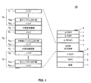
本発明のIII族窒化物半導体琥珀色〜赤色波長発光素子について、本発明の例示的実施形態として図1に示すLEDデバイス構造体の文脈において説明する。図1は、本発明による琥珀色〜赤色III族窒化物LED10の例示的実施形態の一部分の断面図である。琥珀色〜赤色III族窒化物LEDデバイス10は、従来のエピタキシャル法、例えば有機金属化学蒸着(metalorganic chemical vapor deposition:MOCVD)としても公知である有機金属気相成長(metalorganic vapor phase epitaxy:MOVPE)によって製造できる。図1に示すように、およそ2μmのGaNバッファ層2を基板1(例えばサファイア基板)上に成長させ、間に核生成層(図示せず)を挿入する。Siでドープしたおよそ3μm厚のn型GaNクラッド層3を、GaNバッファ層2上に成長させる。琥珀色〜赤色III族窒化物LED10の例示的実施形態は、好適な基板1の結晶方位を用いて、極性、半極性又は非極性結晶方位にエピタキシャル成長させることができる。
The group III nitride semiconductor amber to red wavelength light emitting device of the present invention will be described in the context of the LED device structure shown in FIG. 1 as an exemplary embodiment of the present invention. FIG. 1 is a cross-sectional view of a portion of an exemplary embodiment of an amber-red group III-
図1を参照すると、III族窒化物LED構造体は、発光領域又は多重量子井戸(MQW)活性領域4を備え、これは、n型GaNクラッド層3上に成長させたインジウム含有III族窒化物半導体層を備える。図1に示すように、活性領域4は3タイプのMQWセットを備えてよく、底部MQWセット4Aから最上部MQWセット4Hへとインジウム濃度が漸進的に増大する。各MQWセットは、1つ又は複数の2〜3nm厚の(結晶方位に応じて更に厚くてもよい)InGaN量子井戸層(4A2、...、4E2、...、4H2...)と、主にGaNで構成された1つ又は複数の5〜20nm厚のバリア層(4A1、...、4B、4E1、...、4F、4H1、...、4I)とを含み、上記バリア層は1つずつ交互にスタックされ、各InGaN量子井戸層が2つのバリア層の間に挟まれる。従って、図1に示すように、MQWセット4A、4E、4Hを垂直にスタックしてMQWセット4の多層スタックを生成してよい。III族窒化物系バリア層(4A1、...、4B、4E1、...、4F、4H1、...、4I)は、上記III族窒化物系バリア層の各量子井戸層(4A2、...、4E2、...、4H2...)の量子閉じ込めレベルを調整するために、必要に応じて追加量のインジウム及び/又はアルミニウムを含んでよい。第1のMQWセット4A及び第2のMQWセット4Eのインジウム濃度は好ましくは、図示した例ではそれぞれ7〜13%及び20〜25%の範囲である。最初の2つのMQWセット4A、4Eは、琥珀色〜赤色の発光に好ましい30%超のインジウム濃度を有し得る最上部MQWセット4Hのための予歪み効果を生成する。
Referring to FIG. 1, the III-nitride LED structure comprises a light emitting region or multiple quantum well (MQW) active region 4, which is an indium-containing III-nitride grown on an n-type
本発明の一実施形態では、図1のIII族窒化物琥珀色〜赤色発光構造体の最上部MQWセット4Hの高インジウム含有量子井戸層(4H2、...)の歪みの慎重な制御により、相分離を引き起こすことなく高いインジウム濃度が達成される。この実施形態では、インジウム濃度が漸進的に上昇する下側の2つのMQWセット4A、4Eを導入することにより、バリア層上に予歪み効果が生成されるため、最上部MQWセット4H内の多量のインジウムの取り込みが促進される。インジウム濃度が低いMQWセットをIII族窒化物発光構造体内に1つだけ又は2つ含めても、高いスペクトル純度及び高い出力電力で琥珀色〜赤色の領域において発光する、完全に機能するIII族窒化物半導体LEDは生成できないことを強調しておく。従って、本発明の別の実施形態によると、図1に示すように、中間歪補償層(ISCL)4C、4Gはそれぞれ、2つの連続するMQWセットの間に挿入される。 In one embodiment of the present invention, high-indium-containing quantum well layer of the uppermost MQW set 4 H III nitride amber to red light emitting structure of FIG. 1 (4 H2, ...) careful control of the distortion of the This achieves a high indium concentration without causing phase separation. In this embodiment, by introducing two lower MQW sets 4 A , 4 E with progressively increasing indium concentration, a pre-strain effect is created on the barrier layer, so that the top MQW set 4 H Incorporation of a large amount of indium is promoted. Fully functional III-nitride that emits in the amber to red region with high spectral purity and high output power even if only one or two MQW sets with low indium concentration are included in the III-nitride light emitting structure It is emphasized that physical semiconductor LEDs cannot be produced. Thus, according to another embodiment of the present invention, as shown in FIG. 1, intermediate distortion compensation layers (ISCL) 4 C , 4 G are each inserted between two consecutive MQW sets.
ISCLはそれぞれ、2つの連続するMQWセットのバリア層の間に挟まれ、また好ましくは約17%〜約25%の範囲でAl濃度xが変動するAlxGa1-xN(0<x≦1)合金からなる。好ましくは、ISCL 4C、4Gの厚さ及びAl濃度は異なる。本発明の一実施形態では、下側ISCL 4CのAl濃度xを上側ISCL 4GのAl濃度xより高くすることによって、層に亀裂が発生するのを防ぐことができ、またこれらの層によるLEDデバイス10の過度の直列抵抗を回避できる。本発明の別の実施形態では、下側ISCL 4CのAl濃度xを上側ISCL 4GのAl濃度xより低くすることによって、下側の2つの低インジウム濃度MQWセット4A、4Eへのキャリア注入を抑制でき、これは高インジウム濃度の最上部MQWセット4Hへの、より高いレベルのキャリア注入を促進するのに有利であり、これによって最上部MQWセット4HからのLEDデバイス発光の比率が増大し、従って本発明のIII族窒化物半導体発光素子の琥珀色〜赤色の発光の半値全幅(FWHM)が減少する。一般に、Al濃度はISCL毎に変動するが、代替として、個々の中間歪補償層のAl濃度は、当該中間歪補償層内において、層内の複数の離散的ステップとして(段階的に)又は各層内での連続的変動として、変動してもよい。
Each ISCL is sandwiched between the barrier layers of two successive MQW sets and preferably has an Al x Ga 1-x N (0 <x ≦ 0) where the Al concentration x varies between about 17% and about 25%. 1) Made of an alloy. Preferably, ISCL 4 C , 4 G thickness and Al concentration are different. In an embodiment of the present invention, by making the Al concentration x of the lower ISCL 4 C higher than the Al concentration x of the upper ISCL 4 G , it is possible to prevent the layers from cracking, and due to these layers. Excessive series resistance of the
当業者は、本発明の上述の方法の使用法を認識して、III族窒化物半導体発光素子の琥珀色〜赤色の発光の標的性能パラメータに応じたISCL 4C、4Gの最適な厚さ及びAl濃度を選択するであろう。 Those skilled in the art will recognize the use of the above-described method of the present invention, and the optimum thickness of ISCL 4 C , 4 G depending on the target performance parameter of the amber to red emission of the group III nitride semiconductor light emitting device. And the Al concentration will be selected.
図1に戻ると、LEDデバイス10の重なっているMQW活性領域4は、約200nmの総厚さをそれぞれ有し、またMgドープAlGaN電子ブロック層(electron blocking layer:EBL)5、MgドープGaNクラッド層6、MgドープGaNコンタクト層7を含む、p型層である。p型AlGaN及びGaNクラッド層のMgの原子濃度は好ましくは、例えば1E19cm-3〜1E20cm-3の範囲である。p型GaNコンタクト層のMg原子濃度は好ましくは、例えば1E21cm-3である。
Returning to FIG. 1, the overlapping MQW active regions 4 of the
従来技術のIII族窒化物発光素子におけるように、本発明のIII族窒化物半導体琥珀色〜赤色発光デバイスは、まずエピタキシャル処理済みウェハの上面p−GaN層7上にオーミックコンタクト金属スタックを堆積させてp側電極8を形成し、続いて側部トレンチをエッチングしてn−GaN層3を露出させ、続いてエッチングした上記トレンチ内にオーミックコンタクト金属スタックを堆積させてn側電極9を形成することにより、形成される。続いて上記エピタキシャル処理済みウェハをダイシングして、それぞれ図1に示した断面を実質的に有する個別のLEDチップを形成し、その後これらをパッケージ化し、それぞれのp電極及びn電極にワイヤボンディングして、本発明のLEDデバイスを形成する。実験室での試験のために、p側電極(又はオーミックコンタクト金属スタック)8、例えば(迅速な試験における簡略化のための)インジウムボールを、p型GaNコンタクト層7上に形成する。
As in the group III nitride light emitting device of the prior art, the group III nitride semiconductor amber to red light emitting device of the present invention first deposits an ohmic contact metal stack on the upper p-
更に、デバイス10の一方の側部を、p型GaNコンタクト層7からn型GaNクラッド層3の一部までエッチングする。続いてn側電極(又はオーミックコンタクト金属スタック)9、例えば(迅速な試験における簡略化のための)インジウムボールを、n型GaNクラッド層の露出部分上に形成する。
Further, one side of the
正のp側電極8を通したn側電極9への電流注入下で、電子・正孔再結合プロセスにより、活性領域4から可視光が放出される。本発明の方法に従ってエピタキシャル成長させたIII族窒化物半導体LEDデバイス10は好ましくは、最上部MQWセット4Hのみが光を放出し、その一方で底部の2つのMQWセット4A、4Eが主に予歪み層として機能するように構成される。約30mAの電流注入下で琥珀色〜赤色(琥珀色−赤色)可視スペクトル領域内の光を放出する面積が〜1mm2のIII族窒化物半導体LEDデバイス10は、強い琥珀色−赤色発光を放出する。
Under the current injection into the n-
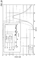
図2aは、約30mAで駆動される図1の琥珀色−赤色LED10の典型的なELスペクトルを示すグラフである。挿入図は、30mA及び100mAの注入電流での短波長スペクトル領域内の、本発明の図1のIII族窒化物LED10の琥珀色LED及び赤色両方の例示的実施形態のELスペクトルを示す。図2(a)の挿入図に見られるように、100mAの比較的高い駆動電力下でさえ、比較的短い波長域に追加のピークが存在せず、これは本発明のLEDに相分離が存在しないことを示唆している。対照的に、従来技術のLEDの性能を示す図2b、2cに示すように、相分離によって誘発される追加の発光ピーク(〜440nm)及び実質的により広いFWHM発光が、従来技術のLED:米国特許出願公開第20110237011A1号及びApp. Phys. Express 7, 071003 (2015)それぞれにおいて容易に観察される。
FIG. 2a is a graph showing a typical EL spectrum of the amber-
図3〜図6は、本発明の琥珀色−赤色III族窒化物発光素子10の性能を実証している。図3、図4は、デバイス10の活性領域4が赤色(〜625nm)発光(〜45%インジウム濃度)のために設計された本発明の一例示的実施形態の性能を実証しており、図5、図6は、琥珀色(〜615nm)発光(〜40%インジウム濃度)のために設計されたデバイス10の活性領域構造を有する本発明の別の例示的実施形態の性能を実証している。
3-6 demonstrate the performance of the amber-red group III nitride
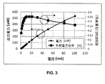
図3は、赤色(〜625nm)発光においてピークに達するよう設計された活性領域4を有する本発明の赤色発光III族窒化物LEDデバイス10に関する、出力電力及び相対EQEの測定された電流依存を示すグラフである。全ての測定は、p側電極8及びn側電極9両方としてインジウムボールを用いたオンウェハ試験構成において実施される。特別な表面処理及び/又は冷却ユニットを用いずに、図示した試験を行った。光はLED10の下に配置された積分球によって集光され、従って全ての光が集光されたわけではなかった。図3に示すように、出力電力は、他のIII族窒化物半導体系LEDにおいて観察されるように、電力規則(power rule)に従って印加された電流と共に増大する。30mAでは、赤色III族窒化物半導体LED10の出力電力は約211μWに達する。赤色III族窒化物半導体LED10の相対EQEはおよそ11mAで約35%のピークに達し、その後電流の増大と共に単調に低下し始める。100mAで、相対EQEはピーク値と比較して約26%だけ低下した。電流の増大に伴うEQE低下の真の機序は、LED設計分野においてまだよく理解されていない。この現象に関して2つの説明が基本的に存在する:(1)オージェ再結合;及び(2)不十分な正孔輸送による電子の漏れ(これに関する詳細な説明は本開示の範囲を超える)。
FIG. 3 shows the measured current dependence of output power and relative EQE for a red emitting III-
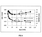
図4は、図1の赤色III族窒化物LED10に関する、測定された発光ピーク波長シフト及びFWHMの例を電流と共に示すグラフである。発光ピーク波長は、注入電流の増大と共に青色シフトを示す。この挙動は、III族窒化物系半導体LEDにおける圧電場のキャリアスクリーニングの特性である。バンド充填効果(band−filling effect)もまた、青色シフトの別の原因である。発光ピーク波長は、強いバンド充填により低い電流でシフトするが、100mAで徐々に飽和して617nmとなる。〜1mm2の面積を有するデバイスに関して、発光ピーク波長は30mAで625nm(赤色)であり、FWHMは同一の電流レベルで49nmの最小値に達する。出願人が知る限りでは、これは、これまでに達成されたIII族窒化物発光素子からの最高の赤色発光性能を示す。
FIG. 4 is a graph showing an example of measured emission peak wavelength shift and FWHM along with current for the red group III-
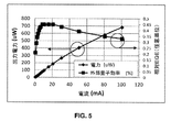
図5は、琥珀色発光においてピークに達するよう設計された活性領域4を有する本発明の図1のIII族窒化物半導体LEDデバイス10の、出力電力及び相対EQEの電流依存を示すグラフである。〜1mm2の領域を有するデバイスに関する、1つ前の例示的実施形態の赤色III族窒化物半導体LEDの挙動と同様の挙動において、琥珀色III族窒化物半導体LEDの相対EQEは、およそ9mAで45%のピークに達し、100mAで約33%まで低下する。琥珀色III族窒化物LEDに関して測定された出力電力は、30mAで約266μWであった。
FIG. 5 is a graph showing the output power and relative EQE current dependence of the III-nitride
図6は、図1の琥珀色III族窒化物半導体LED10に関する、測定された発光ピーク波長及びFWHMの変動の例を、印加された電流と共に示すグラフである。赤色III族窒化物LEDと同様の傾向に従って、波長は低い電流でシフトするが、100mAで飽和して599nmとなる。30mAでピーク波長は617nm(琥珀色)であり、FWHMは54nmである。
FIG. 6 is a graph showing an example of measured emission peak wavelength and FWHM variation, along with applied current, for the amber group III
先行するいくつかの段落に記載したように、本発明による高い出力電力及び高いスペクトル純度を有する琥珀色〜赤色の光を放出するIII族窒化物半導体LEDは、材料の歪みを慎重に制御にすることにより容易に製造できる。エピタキシャル成長法は、III−V化合物半導体を得るための技法に適合する。本開示を実践する際に使用する好適なエピタキシャル堆積技法としては、MOVPE、分子線エピタキシ(molecular beam epitaxy:MBE)、及びハイドライド気相成長(hydride vapor phase epitaxy:HVPE)が挙げられるがこれらに限定されない。III族窒化物系半導体層は例えば、AlxGayIn1-x-yNで構成でき、ここで0≦x≦1及び0≦y≦1である。基板1の面方位は、c面、半極性及び非極性結晶面であってよい。
As described in the preceding paragraphs, III-nitride semiconductor LEDs emitting amber to red light with high output power and high spectral purity according to the present invention carefully control material distortion Can be easily manufactured. The epitaxial growth method is compatible with a technique for obtaining a III-V compound semiconductor. Suitable epitaxial deposition techniques for use in practicing the present disclosure include, but are not limited to, MOVPE, molecular beam epitaxy (MBE), and hydride vapor phase epitaxy (HVPE). Not. The group III nitride semiconductor layer can be made of, for example, Al x Ga y In 1-xy N, where 0 ≦ x ≦ 1 and 0 ≦ y ≦ 1. The plane orientation of the
更に、本開示によるLEDデバイス10は、従来のIII−V化合物半導体の製造方式及び技術を使用して容易に製作できる。
Furthermore, the
以上の開示を例として記載したが、本開示はこれに限定されないことを理解されたい。幅広い修正及び同様の構成を含むことが意図されている。本開示の特徴又は構成要素の修正は、本開示の中核となるコンセプトから逸脱することなく実施できる。その結果として、本開示の範囲は以上の記載によって限定されることはなく、本明細書中で述べたように添付の請求項によってのみ限定される。 While the above disclosure has been described by way of example, it is to be understood that the present disclosure is not limited thereto. It is intended to include a wide range of modifications and similar configurations. Modifications to features or components of the present disclosure can be made without departing from the core concepts of the present disclosure. As a result, the scope of the present disclosure is not limited by the foregoing description, but only by the appended claims as set forth herein.
Claims (23)
第1の前記多重量子井戸セットは、前記基板に隣接し、低いインジウム濃度を有し;
前記第1の多重量子井戸セットの上方の各前記多重量子井戸セットは、漸進的に上昇する濃度を有し;
最上部の前記多重量子井戸セットは、琥珀色〜赤色の光を放出するよう選択された最も高いインジウム濃度を有し;
隣接する前記多重量子井戸セットは、AlxGa1-xN(0<x≦1)中間歪補償層によって隔てられ、各前記AlxGa1-xN(0<x≦1)中間歪補償層は、前記最上部多重量子井戸セットにおける総歪みを低減するために、各前記AlxGa1-xN(0<x≦1)中間歪補償層の上下にバリア層を有する、III族窒化物半導体LED。 Comprising a plurality of multiple quantum well sets stacked on a substrate;
A first set of multiple quantum wells is adjacent to the substrate and has a low indium concentration;
Each of the multiple quantum well sets above the first multiple quantum well set has a progressively increasing concentration;
The top multi-quantum well set has the highest indium concentration selected to emit amber to red light;
Adjacent multiple quantum well sets are separated by Al x Ga 1-x N (0 <x ≦ 1) intermediate strain compensation layers, and each Al x Ga 1-x N (0 <x ≦ 1) intermediate strain compensation. A layer having a barrier layer above and below each Al x Ga 1-x N (0 <x ≦ 1) intermediate strain compensation layer to reduce total strain in the uppermost multiple quantum well set Semiconductor LED.
前記最上部多重量子井戸セットの上の電子ブロック層;
前記電子ブロック層の上のクラッド層;及び
前記クラッド層の上のコンタクト層
を更に備える、請求項1に記載のIII族窒化物半導体LED。 A barrier layer under the first multiple quantum well set;
An electron blocking layer over the top multiple quantum well set;
The group III nitride semiconductor LED according to claim 1, further comprising a cladding layer on the electron blocking layer; and a contact layer on the cladding layer.
複数の多重量子井戸セットを有する活性領域を基板上に形成するステップ
を含み、
前記ステップは:
あるインジウム濃度を有する多重量子井戸の第1のセットを基板上に形成するステップ;
多重量子井戸の少なくとも1つの追加のセットを、前記多重量子井戸の第1のセット上に形成するステップであって、前記多重量子井戸の追加のセットそれぞれの形成の前に、多重量子井戸の先行するセット上におけるAlxGa1-xN(0<x≦1)中間歪補償層の形成を行う、ステップ
によって実施され;
多重量子井戸の最上部セットは、前記多重量子井戸の第1のセットより高いインジウム濃度を有する、方法。 A method of forming a group III nitride semiconductor LED, the method comprising:
Forming an active region having a plurality of multiple quantum well sets on a substrate;
The steps are:
Forming a first set of multiple quantum wells having an indium concentration on a substrate;
Forming at least one additional set of multi-quantum wells on the first set of multi-quantum wells, prior to formation of each additional set of multi-quantum wells, Forming an Al x Ga 1-x N (0 <x ≦ 1) intermediate strain compensation layer on the set to be performed;
The top set of multiple quantum wells has a higher indium concentration than the first set of multiple quantum wells.
前記基板に最も近い第1の前記AlxGa1-xN(0<x≦1)中間歪補償層は、第2の前記AlxGa1-xN(0<x≦1)中間歪補償層より高いAl濃度を有し;
前記第1の多重量子井戸セットは17%以下のインジウム濃度を有し、第2の前記多重量子井戸セットは20%超のインジウム濃度を有し、第3の又は最上部の前記多重量子井戸セットは30%超のインジウム濃度を有する、請求項13に記載の方法。 Forming a barrier layer above and below each of the Al x Ga 1-x N (0 <x ≦ 1) intermediate strain compensation layers, each of the barrier layers being made of GaN, and each of the multiple quantum well sets being Further comprising a step comprised of InGaN;
The first Al x Ga 1-x N (0 <x ≦ 1) intermediate strain compensation layer closest to the substrate is a second Al x Ga 1-x N (0 <x ≦ 1) intermediate strain compensation. Having a higher Al concentration than the layer;
The first multiple quantum well set has an indium concentration of 17% or less, the second multiple quantum well set has an indium concentration greater than 20%, and the third or top multiple quantum well set. 14. The method of claim 13, wherein has an indium concentration greater than 30%.
前記多層III族窒化物半導体LEDは、第1の層状多重量子井戸セット、第2の層状多重量子井戸セット、及び第3の層状多重量子井戸セットを備え;
前記層状多重量子井戸の第1のセットは第1のインジウム濃度を有し;
前記層状多重量子井戸の第2のセットは前記第1のインジウム濃度より高い第2のインジウム濃度を有し;
前記層状多重量子井戸の第3のセットは前記第2のインジウム濃度より高い第3のインジウム濃度を有し;
前記多層III族窒化物半導体LEDは:
前記第1の層状多重量子井戸セットと前記第2の層状多重量子井戸セットとの間に配置される、AlxGa1-xN(0<x≦1)で構成された第1の中間歪補償層;
前記第2の層状多重量子井戸セットと前記第3の層状多重量子井戸セットとの間に配置される、AlxGa1-xN(0<x≦1)で構成された第2の中間歪補償層
を備え、
前記第1の中間歪補償層及び前記第2の中間歪補償層はそれぞれ2つのバリア層の間に配置され、
前記第3の層状多重量子井戸セットは、およそ600nm〜およそ660nmの範囲の波長においてピーク発光を有する光を放出するよう構成される、多層III族窒化物半導体LED。 A multilayer III-nitride semiconductor LED comprising:
The multilayer III-nitride semiconductor LED comprises a first layered multiple quantum well set, a second layered multiple quantum well set, and a third layered multiple quantum well set;
The first set of layered multiple quantum wells has a first indium concentration;
The second set of layered multiple quantum wells has a second indium concentration that is higher than the first indium concentration;
The third set of layered multiple quantum wells has a third indium concentration that is higher than the second indium concentration;
The multilayer III-nitride semiconductor LED is:
A first intermediate strain composed of Al x Ga 1-x N (0 <x ≦ 1), disposed between the first layered multiple quantum well set and the second layered multiple quantum well set. Compensation layer;
A second intermediate strain composed of Al x Ga 1-x N (0 <x ≦ 1), disposed between the second layered multiple quantum well set and the third layered multiple quantum well set. With a compensation layer,
The first intermediate strain compensation layer and the second intermediate strain compensation layer are each disposed between two barrier layers;
The third layered multiple quantum well set is a multi-layer III-nitride semiconductor LED configured to emit light having a peak emission at a wavelength in the range of approximately 600 nm to approximately 660 nm.
第1のバリア層を画定するステップ;
前記第1のバリア層上に、第1のインジウム濃度を有する第1の層状多重量子井戸セットを画定するステップ;
前記第1の層状多重量子井戸セット上に第2のバリア層を画定するステップ;
前記第2のバリア層上に、AlxGa1-xN(0<x≦1)で構成された第1の中間歪補償層を画定するステップ;
前記第1の中間歪補償層上に第3のバリア層を画定するステップ;
前記第3のバリア層上に、前記第1のインジウム濃度より高い第2のインジウム濃度を有する第2の層状多重量子井戸セットを画定するステップ;
前記第2の層状多重量子井戸セット上に第4のバリア層を画定するステップ;
前記第4のバリア層上に、AlxGa1-xN(0<x≦1)で構成された第2の中間歪補償層を画定するステップ;
前記第2の中間歪補償層上に第5のバリア層を画定するステップ;
およそ600nm〜およそ660nmの範囲の波長においてピーク発光を有する光を放出するよう構成された、前記第2のインジウム濃度より高い第3のインジウム濃度を有する、第3の層状多重量子井戸セットを画定するステップ
を含む、方法。 A method of manufacturing a group III nitride semiconductor LED that emits amber to red light, the method comprising:
Defining a first barrier layer;
Defining a first layered multiple quantum well set having a first indium concentration on the first barrier layer;
Defining a second barrier layer on the first layered multiple quantum well set;
Defining a first intermediate strain compensation layer made of Al x Ga 1-x N (0 <x ≦ 1) on the second barrier layer;
Defining a third barrier layer on the first intermediate strain compensation layer;
Defining a second layered multiple quantum well set having a second indium concentration higher than the first indium concentration on the third barrier layer;
Defining a fourth barrier layer on the second layered multiple quantum well set;
Defining a second intermediate strain compensation layer made of Al x Ga 1-x N (0 <x ≦ 1) on the fourth barrier layer;
Defining a fifth barrier layer on the second intermediate strain compensation layer;
Defining a third layered multi-quantum well set having a third indium concentration higher than the second indium concentration configured to emit light having a peak emission at a wavelength in a range of approximately 600 nm to approximately 660 nm. A method comprising steps.
Priority Applications (1)
| Application Number | Priority Date | Filing Date | Title |
|---|---|---|---|
| JP2022036024A JP2022071179A (en) | 2015-10-08 | 2022-03-09 | Iii-nitride semiconductor light emitting led having amber-to-red light emission |
Applications Claiming Priority (5)
| Application Number | Priority Date | Filing Date | Title |
|---|---|---|---|
| US201562239122P | 2015-10-08 | 2015-10-08 | |
| US62/239,122 | 2015-10-08 | ||
| US15/287,384 US10396240B2 (en) | 2015-10-08 | 2016-10-06 | III-nitride semiconductor light emitting device having amber-to-red light emission (>600 nm) and a method for making same |
| US15/287,384 | 2016-10-06 | ||
| PCT/US2016/056157 WO2017062889A1 (en) | 2015-10-08 | 2016-10-07 | III-NITRIDE SEMICONDUCTOR LIGHT EMITTING DEVICE HAVING AMBER-TO-RED LIGHT EMISSION (>600 nm) AND A METHOD FOR MAKING SAME |
Related Child Applications (1)
| Application Number | Title | Priority Date | Filing Date |
|---|---|---|---|
| JP2022036024A Division JP2022071179A (en) | 2015-10-08 | 2022-03-09 | Iii-nitride semiconductor light emitting led having amber-to-red light emission |
Publications (3)
| Publication Number | Publication Date |
|---|---|
| JP2018531514A true JP2018531514A (en) | 2018-10-25 |
| JP2018531514A6 JP2018531514A6 (en) | 2018-12-13 |
| JP2018531514A5 JP2018531514A5 (en) | 2019-11-14 |
Family
ID=57184854
Family Applications (2)
| Application Number | Title | Priority Date | Filing Date |
|---|---|---|---|
| JP2018517812A Pending JP2018531514A (en) | 2015-10-08 | 2016-10-07 | Group III nitride semiconductor light emitting device having amber to red emission (> 600 nm) and method for making the same |
| JP2022036024A Pending JP2022071179A (en) | 2015-10-08 | 2022-03-09 | Iii-nitride semiconductor light emitting led having amber-to-red light emission |
Family Applications After (1)
| Application Number | Title | Priority Date | Filing Date |
|---|---|---|---|
| JP2022036024A Pending JP2022071179A (en) | 2015-10-08 | 2022-03-09 | Iii-nitride semiconductor light emitting led having amber-to-red light emission |
Country Status (8)
| Country | Link |
|---|---|
| US (1) | US10396240B2 (en) |
| EP (1) | EP3360168B1 (en) |
| JP (2) | JP2018531514A (en) |
| KR (1) | KR20180067590A (en) |
| CN (1) | CN108292693B (en) |
| HK (1) | HK1258318A1 (en) |
| TW (1) | TWI775729B (en) |
| WO (1) | WO2017062889A1 (en) |
Families Citing this family (11)
| Publication number | Priority date | Publication date | Assignee | Title |
|---|---|---|---|---|
| JP2018516466A (en) | 2015-06-05 | 2018-06-21 | オステンド・テクノロジーズ・インコーポレーテッド | Light-emitting structure with selected carrier injection into multiple active layers |
| US10971652B2 (en) * | 2017-01-26 | 2021-04-06 | Epistar Corporation | Semiconductor device comprising electron blocking layers |
| US11056434B2 (en) | 2017-01-26 | 2021-07-06 | Epistar Corporation | Semiconductor device having specified p-type dopant concentration profile |
| WO2019130753A1 (en) * | 2017-12-27 | 2019-07-04 | オリンパス株式会社 | Light source device |
| FR3089686B1 (en) * | 2018-12-11 | 2020-11-13 | Aledia | Optoelectronic device comprising pixels emitting three colors |
| US11404473B2 (en) | 2019-12-23 | 2022-08-02 | Lumileds Llc | III-nitride multi-wavelength LED arrays |
| US11923398B2 (en) | 2019-12-23 | 2024-03-05 | Lumileds Llc | III-nitride multi-wavelength LED arrays |
| WO2021226121A1 (en) * | 2020-05-04 | 2021-11-11 | Raxium, Inc. | Light emitting diodes with aluminum-containing layers integrated therein and associated methods |
| US11876150B2 (en) | 2020-05-19 | 2024-01-16 | Google Llc | Combination of strain management layers for light emitting elements |
| US11264535B1 (en) * | 2020-08-12 | 2022-03-01 | Jyh-Chia Chen | Pixel device and display using a monolithic blue/green LED combined with red luminescence materials |
| US11631786B2 (en) | 2020-11-12 | 2023-04-18 | Lumileds Llc | III-nitride multi-wavelength LED arrays with etch stop layer |
Citations (17)
| Publication number | Priority date | Publication date | Assignee | Title |
|---|---|---|---|---|
| US5684309A (en) * | 1996-07-11 | 1997-11-04 | North Carolina State University | Stacked quantum well aluminum indium gallium nitride light emitting diodes |
| JPH1187773A (en) * | 1997-09-08 | 1999-03-30 | Toshiba Corp | Light emitting element |
| JP2002176198A (en) * | 2000-12-11 | 2002-06-21 | Mitsubishi Cable Ind Ltd | Multi-wavelength light emitting element |
| JP2004253801A (en) * | 2003-02-18 | 2004-09-09 | Agilent Technol Inc | InGaAsN DEVICE WITH IMPROVED WAVELENGTH STABILITY |
| JP2007123878A (en) * | 2005-10-25 | 2007-05-17 | Samsung Electro Mech Co Ltd | Nitride semiconductor light-emitting element |
| JP2007180499A (en) * | 2005-12-28 | 2007-07-12 | Samsung Electro Mech Co Ltd | Nitride semiconductor light-emitting device |
| JP2008311658A (en) * | 2007-06-12 | 2008-12-25 | Seoul Opto Devices Co Ltd | Light emitting diode having active region of multiple quantum well structure |
| JP2009224370A (en) * | 2008-03-13 | 2009-10-01 | Rohm Co Ltd | Nitride semiconductor device |
| JP2010141242A (en) * | 2008-12-15 | 2010-06-24 | Opnext Japan Inc | Nitride semiconductor optical element and manufacturing method thereof |
| JP2011517099A (en) * | 2008-04-04 | 2011-05-26 | ザ リージェンツ オブ ザ ユニバーシティ オブ カリフォルニア | MOCVD growth technology for planar semipolar (Al, In, Ga, B) N-based light-emitting diodes |
| JP2011517098A (en) * | 2008-04-04 | 2011-05-26 | ザ リージェンツ オブ ザ ユニバーシティ オブ カリフォルニア | Method for the production of semipolar (Al, In, Ga, B) N-based light emitting diodes |
| US20110133156A1 (en) * | 2009-12-07 | 2011-06-09 | Jong Hak Won | Light emitting device and light emitting device package including the same |
| JP2011176240A (en) * | 2010-02-25 | 2011-09-08 | Toshiba Corp | Semiconductor light emitting device, and method of manufacturing the same |
| JP2013502731A (en) * | 2009-08-21 | 2013-01-24 | ザ リージェンツ オブ ザ ユニバーシティ オブ カリフォルニア | Anisotropic strain control of semipolar nitride quantum wells with partially or fully relaxed AlInGaN layers with misfit dislocations |
| JP2013140966A (en) * | 2011-12-30 | 2013-07-18 | Iljin Led Co Ltd | Nitride-based light emitting element with excellent luminous efficiency using strain buffer layer |
| JP2014090169A (en) * | 2012-10-16 | 2014-05-15 | Soraa Inc | Indium gallium nitride light-emitting device |
| JP2014103391A (en) * | 2012-11-21 | 2014-06-05 | Shogen Koden Kofun Yugenkoshi | Light-emitting device having a plurality of light-emitting stack layers |
Family Cites Families (63)
| Publication number | Priority date | Publication date | Assignee | Title |
|---|---|---|---|---|
| US4839899A (en) | 1988-03-09 | 1989-06-13 | Xerox Corporation | Wavelength tuning of multiple quantum well (MQW) heterostructure lasers |
| JPH04350988A (en) * | 1991-05-29 | 1992-12-04 | Nec Kansai Ltd | Light-emitting element of quantum well structure |
| US5422898A (en) | 1993-10-29 | 1995-06-06 | International Business Machines Corporation | Tapered Fabry-Perot multi-wavelength optical source |
| US5386428A (en) | 1993-11-02 | 1995-01-31 | Xerox Corporation | Stacked active region laser array for multicolor emissions |
| US5737353A (en) | 1993-11-26 | 1998-04-07 | Nec Corporation | Multiquantum-well semiconductor laser |
| JP2682474B2 (en) * | 1993-11-26 | 1997-11-26 | 日本電気株式会社 | Semiconductor laser device |
| JPH08316588A (en) | 1995-05-23 | 1996-11-29 | Furukawa Electric Co Ltd:The | Semiconductor optical element having strained quantum well structure |
| TW412889B (en) | 1997-09-24 | 2000-11-21 | Nippon Oxygen Co Ltd | Semiconductor laser |
| WO2000058999A2 (en) | 1999-03-26 | 2000-10-05 | Matsushita Electric Industrial Co., Ltd. | Semiconductor structures having a strain compensated layer and method of fabrication |
| US7202506B1 (en) | 1999-11-19 | 2007-04-10 | Cree, Inc. | Multi element, multi color solid state LED/laser |
| NL1015860C2 (en) * | 2000-08-02 | 2002-02-05 | Wavin Bv | Methods and devices for manufacturing a tube of biaxially oriented thermoplastic plastic material with an integral sleeve. |
| US6469358B1 (en) | 2000-09-21 | 2002-10-22 | Lockheed Martin Corporation | Three color quantum well focal plane arrays |
| EP1385241B1 (en) | 2001-03-28 | 2008-12-31 | Nichia Corporation | Nitride semiconductor element |
| JP2004146498A (en) | 2002-10-23 | 2004-05-20 | Stanley Electric Co Ltd | Semiconductor light-emitting device |
| CA2427559A1 (en) | 2002-05-15 | 2003-11-15 | Sumitomo Electric Industries, Ltd. | White color light emitting device |
| US7058105B2 (en) | 2002-10-17 | 2006-06-06 | Samsung Electro-Mechanics Co., Ltd. | Semiconductor optoelectronic device |
| US6927412B2 (en) | 2002-11-21 | 2005-08-09 | Ricoh Company, Ltd. | Semiconductor light emitter |
| JP4571372B2 (en) * | 2002-11-27 | 2010-10-27 | ローム株式会社 | Semiconductor light emitting device |
| US6919584B2 (en) | 2003-06-19 | 2005-07-19 | Harvatek Corporation | White light source |
| KR100482511B1 (en) | 2004-02-05 | 2005-04-14 | 에피밸리 주식회사 | Ⅲ-Nitride compound semiconductor light emitting device |
| US7323721B2 (en) | 2004-09-09 | 2008-01-29 | Blue Photonics Inc. | Monolithic multi-color, multi-quantum well semiconductor LED |
| US8148713B2 (en) | 2008-04-04 | 2012-04-03 | The Regents Of The University Of California | Method for fabrication of semipolar (Al, In, Ga, B)N based light emitting diodes |
| KR20070080696A (en) | 2006-02-08 | 2007-08-13 | 삼성전자주식회사 | Nitride based semiconductor laser diode |
| KR100774200B1 (en) | 2006-04-13 | 2007-11-08 | 엘지전자 주식회사 | Organic Electroluminescence Device and method for fabricating the same |
| US7593436B2 (en) | 2006-06-16 | 2009-09-22 | Vi Systems Gmbh | Electrooptically Bragg-reflector stopband-tunable optoelectronic device for high-speed data transfer |
| KR20080035865A (en) * | 2006-10-20 | 2008-04-24 | 삼성전자주식회사 | Semiconductor light emitting device |
| TWI338382B (en) | 2006-11-29 | 2011-03-01 | Univ Nat Taiwan | Method and structure for manufacturing long-wavelength light-emitting diode using prestrain effect |
| KR100862497B1 (en) | 2006-12-26 | 2008-10-08 | 삼성전기주식회사 | Nitride semiconductor device |
| JP2008235606A (en) | 2007-03-20 | 2008-10-02 | Sony Corp | Semiconductor light-emitting element, method for manufacturing semiconductor light-emitting element, backlight, display unit, electronic equipment, and light-emitting device |
| US7623560B2 (en) | 2007-09-27 | 2009-11-24 | Ostendo Technologies, Inc. | Quantum photonic imagers and methods of fabrication thereof |
| GB2456756A (en) | 2008-01-16 | 2009-07-29 | Sharp Kk | AlInGaN Light-Emitting devices |
| JP4720834B2 (en) | 2008-02-25 | 2011-07-13 | 住友電気工業株式会社 | Group III nitride semiconductor laser |
| US20100006873A1 (en) | 2008-06-25 | 2010-01-14 | Soraa, Inc. | HIGHLY POLARIZED WHITE LIGHT SOURCE BY COMBINING BLUE LED ON SEMIPOLAR OR NONPOLAR GaN WITH YELLOW LED ON SEMIPOLAR OR NONPOLAR GaN |
| WO2010020065A1 (en) | 2008-08-19 | 2010-02-25 | Lattice Power (Jiangxi) Corporation | Method for fabricating ingan-based multi-quantum well layers |
| JP4775455B2 (en) * | 2009-02-17 | 2011-09-21 | 住友電気工業株式会社 | Group III nitride semiconductor laser and method of fabricating group III nitride semiconductor laser |
| US9153790B2 (en) | 2009-05-22 | 2015-10-06 | Idemitsu Kosan Co., Ltd. | Organic electroluminescent device |
| US8296624B2 (en) * | 2009-06-30 | 2012-10-23 | Comcast Cable Communications, Llc | Variable interleave data transmission |
| US8314429B1 (en) | 2009-09-14 | 2012-11-20 | Soraa, Inc. | Multi color active regions for white light emitting diode |
| US9484197B2 (en) | 2009-10-23 | 2016-11-01 | The Royal Institution For The Advancement Of Learning/Mcgill University | Lateral growth semiconductor method and devices |
| JP5060656B2 (en) | 2009-12-21 | 2012-10-31 | 株式会社東芝 | Nitride semiconductor light emitting device and manufacturing method thereof |
| TWI508621B (en) | 2010-02-03 | 2015-11-11 | Innolux Corp | System for displaying images |
| US20110188528A1 (en) | 2010-02-04 | 2011-08-04 | Ostendo Technologies, Inc. | High Injection Efficiency Polar and Non-Polar III-Nitrides Light Emitters |
| US8451877B1 (en) | 2010-03-23 | 2013-05-28 | Sandia Corporation | High efficiency III-nitride light-emitting diodes |
| US20110237011A1 (en) | 2010-03-29 | 2011-09-29 | Nanjing University | Method for Forming a GaN-Based Quantum-Well LED with Red Light |
| JP5533744B2 (en) * | 2010-03-31 | 2014-06-25 | 豊田合成株式会社 | Group III nitride semiconductor light emitting device |
| US20120000866A1 (en) * | 2010-06-30 | 2012-01-05 | Randal Huszczo | Glass Storage and Transport Rack with Pivoting Arms |
| JP5372045B2 (en) | 2011-02-25 | 2013-12-18 | 株式会社東芝 | Semiconductor light emitting device |
| JP5737111B2 (en) * | 2011-03-30 | 2015-06-17 | 豊田合成株式会社 | Group III nitride semiconductor light emitting device |
| KR20140039032A (en) | 2011-06-10 | 2014-03-31 | 더 리전츠 오브 더 유니버시티 오브 캘리포니아 | Low droop light emitting diode structure on gallium nitride semipolar substrates |
| US8927958B2 (en) * | 2011-07-12 | 2015-01-06 | Epistar Corporation | Light-emitting element with multiple light-emitting stacked layers |
| GB201112792D0 (en) * | 2011-07-26 | 2011-09-07 | Smith Michael | A ratchet buckle use for the tightening of straps |
| US9070613B2 (en) | 2011-09-07 | 2015-06-30 | Lg Innotek Co., Ltd. | Light emitting device |
| TWI612687B (en) | 2011-09-29 | 2018-01-21 | 晶元光電股份有限公司 | Light-emitting device |
| JP6136284B2 (en) | 2012-03-13 | 2017-05-31 | 株式会社リコー | Semiconductor laminate and surface emitting laser element |
| US9124062B2 (en) * | 2012-03-22 | 2015-09-01 | Palo Alto Research Center Incorporated | Optically pumped surface emitting lasers incorporating high reflectivity/bandwidth limited reflector |
| KR101936305B1 (en) | 2012-09-24 | 2019-01-08 | 엘지이노텍 주식회사 | Light emitting device |
| JP2014067893A (en) * | 2012-09-26 | 2014-04-17 | Toyoda Gosei Co Ltd | Group iii nitride semiconductor light-emitting element |
| US8890114B2 (en) | 2012-10-16 | 2014-11-18 | Epistar Corporation | Light-emitting device |
| WO2014073583A1 (en) | 2012-11-06 | 2014-05-15 | Canon Kabushiki Kaisha | Photonic device and optical coherence tomography apparatus including the photonic device as light source |
| US8941111B2 (en) | 2012-12-21 | 2015-01-27 | Invensas Corporation | Non-crystalline inorganic light emitting diode |
| WO2014138904A1 (en) | 2013-03-14 | 2014-09-18 | The Royal Institution For The Advancement Of Learning/Mcgill University | Methods and devices for solid state nanowire devices |
| US10839734B2 (en) | 2013-12-23 | 2020-11-17 | Universal Display Corporation | OLED color tuning by driving mode variation |
| JP2018516466A (en) | 2015-06-05 | 2018-06-21 | オステンド・テクノロジーズ・インコーポレーテッド | Light-emitting structure with selected carrier injection into multiple active layers |
-
2016
- 2016-10-06 US US15/287,384 patent/US10396240B2/en not_active Expired - Fee Related
- 2016-10-07 JP JP2018517812A patent/JP2018531514A/en active Pending
- 2016-10-07 EP EP16784685.6A patent/EP3360168B1/en active Active
- 2016-10-07 KR KR1020187013012A patent/KR20180067590A/en not_active Application Discontinuation
- 2016-10-07 TW TW105132658A patent/TWI775729B/en active
- 2016-10-07 CN CN201680072137.5A patent/CN108292693B/en not_active Expired - Fee Related
- 2016-10-07 WO PCT/US2016/056157 patent/WO2017062889A1/en active Application Filing
-
2019
- 2019-01-16 HK HK19100686.8A patent/HK1258318A1/en unknown
-
2022
- 2022-03-09 JP JP2022036024A patent/JP2022071179A/en active Pending
Patent Citations (18)
| Publication number | Priority date | Publication date | Assignee | Title |
|---|---|---|---|---|
| US5684309A (en) * | 1996-07-11 | 1997-11-04 | North Carolina State University | Stacked quantum well aluminum indium gallium nitride light emitting diodes |
| JPH1187773A (en) * | 1997-09-08 | 1999-03-30 | Toshiba Corp | Light emitting element |
| JP2002176198A (en) * | 2000-12-11 | 2002-06-21 | Mitsubishi Cable Ind Ltd | Multi-wavelength light emitting element |
| JP2004253801A (en) * | 2003-02-18 | 2004-09-09 | Agilent Technol Inc | InGaAsN DEVICE WITH IMPROVED WAVELENGTH STABILITY |
| JP2007123878A (en) * | 2005-10-25 | 2007-05-17 | Samsung Electro Mech Co Ltd | Nitride semiconductor light-emitting element |
| JP2007180499A (en) * | 2005-12-28 | 2007-07-12 | Samsung Electro Mech Co Ltd | Nitride semiconductor light-emitting device |
| JP2008311658A (en) * | 2007-06-12 | 2008-12-25 | Seoul Opto Devices Co Ltd | Light emitting diode having active region of multiple quantum well structure |
| JP2009224370A (en) * | 2008-03-13 | 2009-10-01 | Rohm Co Ltd | Nitride semiconductor device |
| JP2011517098A (en) * | 2008-04-04 | 2011-05-26 | ザ リージェンツ オブ ザ ユニバーシティ オブ カリフォルニア | Method for the production of semipolar (Al, In, Ga, B) N-based light emitting diodes |
| JP2011517099A (en) * | 2008-04-04 | 2011-05-26 | ザ リージェンツ オブ ザ ユニバーシティ オブ カリフォルニア | MOCVD growth technology for planar semipolar (Al, In, Ga, B) N-based light-emitting diodes |
| JP2010141242A (en) * | 2008-12-15 | 2010-06-24 | Opnext Japan Inc | Nitride semiconductor optical element and manufacturing method thereof |
| JP2013502731A (en) * | 2009-08-21 | 2013-01-24 | ザ リージェンツ オブ ザ ユニバーシティ オブ カリフォルニア | Anisotropic strain control of semipolar nitride quantum wells with partially or fully relaxed AlInGaN layers with misfit dislocations |
| JP2013502730A (en) * | 2009-08-21 | 2013-01-24 | ザ リージェンツ オブ ザ ユニバーシティ オブ カリフォルニア | Semipolar nitride-based devices on partially or fully relaxed alloys with misfit dislocations at the heterointerface |
| US20110133156A1 (en) * | 2009-12-07 | 2011-06-09 | Jong Hak Won | Light emitting device and light emitting device package including the same |
| JP2011176240A (en) * | 2010-02-25 | 2011-09-08 | Toshiba Corp | Semiconductor light emitting device, and method of manufacturing the same |
| JP2013140966A (en) * | 2011-12-30 | 2013-07-18 | Iljin Led Co Ltd | Nitride-based light emitting element with excellent luminous efficiency using strain buffer layer |
| JP2014090169A (en) * | 2012-10-16 | 2014-05-15 | Soraa Inc | Indium gallium nitride light-emitting device |
| JP2014103391A (en) * | 2012-11-21 | 2014-06-05 | Shogen Koden Kofun Yugenkoshi | Light-emitting device having a plurality of light-emitting stack layers |
Also Published As
| Publication number | Publication date |
|---|---|
| EP3360168B1 (en) | 2021-09-29 |
| CN108292693B (en) | 2021-10-22 |
| KR20180067590A (en) | 2018-06-20 |
| WO2017062889A1 (en) | 2017-04-13 |
| TWI775729B (en) | 2022-09-01 |
| US20170104128A1 (en) | 2017-04-13 |
| HK1258318A1 (en) | 2019-11-08 |
| JP2022071179A (en) | 2022-05-13 |
| CN108292693A (en) | 2018-07-17 |
| EP3360168A1 (en) | 2018-08-15 |
| US10396240B2 (en) | 2019-08-27 |
| TW201735390A (en) | 2017-10-01 |
Similar Documents
| Publication | Publication Date | Title |
|---|---|---|
| US10396240B2 (en) | III-nitride semiconductor light emitting device having amber-to-red light emission (>600 nm) and a method for making same | |
| JP2018531514A6 (en) | Group III nitride semiconductor light emitting device having amber to red emission (> 600 nm) and method for making the same | |
| JP6589987B2 (en) | Nitride semiconductor light emitting device | |
| US8227790B2 (en) | Group III nitride semiconductor light-emitting device | |
| US9263632B2 (en) | Semiconductor light emitting device | |
| WO2013084926A1 (en) | Nitride semiconductor light-emitting element and method for producing same | |
| US20160372631A1 (en) | Light emitting diode | |
| JP6433247B2 (en) | Semiconductor light emitting device | |
| JP2013140966A (en) | Nitride-based light emitting element with excellent luminous efficiency using strain buffer layer | |
| JP2014525682A (en) | Optoelectronic parts | |
| KR20110102118A (en) | Semiconductor light-emitting device and method for manufacturing same | |
| JP2008118049A (en) | GaN-BASED SEMICONDUCTOR LIGHT EMITTING DEVICE | |
| US8164109B2 (en) | Nitride semiconductor element and method for producing the same | |
| WO2018163824A1 (en) | Semiconductor light-emitting element and method for manufacturing semiconductor light-emitting element | |
| KR101485690B1 (en) | Semiconductor light emitting device and method for manufacturing the same | |
| WO2011101929A1 (en) | Semiconductor light-emitting device and method for manufacturing the same | |
| JP5380516B2 (en) | Nitride semiconductor light emitting device | |
| JP2009105423A (en) | Group iii nitride semiconductor light emitting device | |
| JP2008227103A (en) | GaN-BASED SEMICONDUCTOR LIGHT EMITTING ELEMENT | |
| KR20090056319A (en) | Nitride compound semiconductor light-emitting device with a superlattice structure | |
| JP6482388B2 (en) | Nitride semiconductor light emitting device | |
| JP5865827B2 (en) | Semiconductor light emitting device | |
| JP2007201146A (en) | Light emitting element and its manufacturing method | |
| US20150243845A1 (en) | Light-emitting device | |
| Okuno et al. | Emission Mechanism of Light‐Emitting Diode Structures with Red, Green, and Blue Active Layers Separated by Si‐Doped Interlayers |
Legal Events
| Date | Code | Title | Description |
|---|---|---|---|
| A521 | Request for written amendment filed |
Free format text: JAPANESE INTERMEDIATE CODE: A523 Effective date: 20191007 |
|
| A621 | Written request for application examination |
Free format text: JAPANESE INTERMEDIATE CODE: A621 Effective date: 20191007 |
|
| A977 | Report on retrieval |
Free format text: JAPANESE INTERMEDIATE CODE: A971007 Effective date: 20201030 |
|
| A131 | Notification of reasons for refusal |
Free format text: JAPANESE INTERMEDIATE CODE: A131 Effective date: 20201215 |
|
| A601 | Written request for extension of time |
Free format text: JAPANESE INTERMEDIATE CODE: A601 Effective date: 20210315 |
|
| A521 | Request for written amendment filed |
Free format text: JAPANESE INTERMEDIATE CODE: A523 Effective date: 20210517 |
|
| A02 | Decision of refusal |
Free format text: JAPANESE INTERMEDIATE CODE: A02 Effective date: 20211109 |