CN108292693B - Group III nitride semiconductor light emitting devices with amber to red (> 600 nm) light emission and methods for making the same - Google Patents
Group III nitride semiconductor light emitting devices with amber to red (> 600 nm) light emission and methods for making the same Download PDFInfo
- Publication number
- CN108292693B CN108292693B CN201680072137.5A CN201680072137A CN108292693B CN 108292693 B CN108292693 B CN 108292693B CN 201680072137 A CN201680072137 A CN 201680072137A CN 108292693 B CN108292693 B CN 108292693B
- Authority
- CN
- China
- Prior art keywords
- quantum well
- well layers
- indium concentration
- layers
- layer
- Prior art date
- Legal status (The legal status is an assumption and is not a legal conclusion. Google has not performed a legal analysis and makes no representation as to the accuracy of the status listed.)
- Expired - Fee Related
Links
Images


Classifications
-
- H—ELECTRICITY
- H01—ELECTRIC ELEMENTS
- H01L—SEMICONDUCTOR DEVICES NOT COVERED BY CLASS H10
- H01L33/00—Semiconductor devices with at least one potential-jump barrier or surface barrier specially adapted for light emission; Processes or apparatus specially adapted for the manufacture or treatment thereof or of parts thereof; Details thereof
- H01L33/005—Processes
- H01L33/0062—Processes for devices with an active region comprising only III-V compounds
- H01L33/0075—Processes for devices with an active region comprising only III-V compounds comprising nitride compounds
-
- H—ELECTRICITY
- H01—ELECTRIC ELEMENTS
- H01L—SEMICONDUCTOR DEVICES NOT COVERED BY CLASS H10
- H01L33/00—Semiconductor devices with at least one potential-jump barrier or surface barrier specially adapted for light emission; Processes or apparatus specially adapted for the manufacture or treatment thereof or of parts thereof; Details thereof
- H01L33/02—Semiconductor devices with at least one potential-jump barrier or surface barrier specially adapted for light emission; Processes or apparatus specially adapted for the manufacture or treatment thereof or of parts thereof; Details thereof characterised by the semiconductor bodies
- H01L33/04—Semiconductor devices with at least one potential-jump barrier or surface barrier specially adapted for light emission; Processes or apparatus specially adapted for the manufacture or treatment thereof or of parts thereof; Details thereof characterised by the semiconductor bodies with a quantum effect structure or superlattice, e.g. tunnel junction
- H01L33/06—Semiconductor devices with at least one potential-jump barrier or surface barrier specially adapted for light emission; Processes or apparatus specially adapted for the manufacture or treatment thereof or of parts thereof; Details thereof characterised by the semiconductor bodies with a quantum effect structure or superlattice, e.g. tunnel junction within the light emitting region, e.g. quantum confinement structure or tunnel barrier
-
- H—ELECTRICITY
- H01—ELECTRIC ELEMENTS
- H01L—SEMICONDUCTOR DEVICES NOT COVERED BY CLASS H10
- H01L33/00—Semiconductor devices with at least one potential-jump barrier or surface barrier specially adapted for light emission; Processes or apparatus specially adapted for the manufacture or treatment thereof or of parts thereof; Details thereof
- H01L33/02—Semiconductor devices with at least one potential-jump barrier or surface barrier specially adapted for light emission; Processes or apparatus specially adapted for the manufacture or treatment thereof or of parts thereof; Details thereof characterised by the semiconductor bodies
- H01L33/12—Semiconductor devices with at least one potential-jump barrier or surface barrier specially adapted for light emission; Processes or apparatus specially adapted for the manufacture or treatment thereof or of parts thereof; Details thereof characterised by the semiconductor bodies with a stress relaxation structure, e.g. buffer layer
-
- H—ELECTRICITY
- H01—ELECTRIC ELEMENTS
- H01L—SEMICONDUCTOR DEVICES NOT COVERED BY CLASS H10
- H01L33/00—Semiconductor devices with at least one potential-jump barrier or surface barrier specially adapted for light emission; Processes or apparatus specially adapted for the manufacture or treatment thereof or of parts thereof; Details thereof
- H01L33/02—Semiconductor devices with at least one potential-jump barrier or surface barrier specially adapted for light emission; Processes or apparatus specially adapted for the manufacture or treatment thereof or of parts thereof; Details thereof characterised by the semiconductor bodies
- H01L33/14—Semiconductor devices with at least one potential-jump barrier or surface barrier specially adapted for light emission; Processes or apparatus specially adapted for the manufacture or treatment thereof or of parts thereof; Details thereof characterised by the semiconductor bodies with a carrier transport control structure, e.g. highly-doped semiconductor layer or current-blocking structure
- H01L33/145—Semiconductor devices with at least one potential-jump barrier or surface barrier specially adapted for light emission; Processes or apparatus specially adapted for the manufacture or treatment thereof or of parts thereof; Details thereof characterised by the semiconductor bodies with a carrier transport control structure, e.g. highly-doped semiconductor layer or current-blocking structure with a current-blocking structure
-
- H—ELECTRICITY
- H01—ELECTRIC ELEMENTS
- H01L—SEMICONDUCTOR DEVICES NOT COVERED BY CLASS H10
- H01L33/00—Semiconductor devices with at least one potential-jump barrier or surface barrier specially adapted for light emission; Processes or apparatus specially adapted for the manufacture or treatment thereof or of parts thereof; Details thereof
- H01L33/02—Semiconductor devices with at least one potential-jump barrier or surface barrier specially adapted for light emission; Processes or apparatus specially adapted for the manufacture or treatment thereof or of parts thereof; Details thereof characterised by the semiconductor bodies
- H01L33/26—Materials of the light emitting region
- H01L33/30—Materials of the light emitting region containing only elements of group III and group V of the periodic system
- H01L33/32—Materials of the light emitting region containing only elements of group III and group V of the periodic system containing nitrogen
Abstract
A group III nitride semiconductor light-emitting device incorporatingnGroup III nitride-type cladding layer, indium-containing group III nitride light-emitting region, andpa type III nitride cap layer. The light emitting region is sandwiched betweenn-andp-type III-nitride cladding layers, and comprising multiple sets of Multiple Quantum Wells (MQW). In thatnThe first MQW set formed on the cladding layer includes a relatively low indium concentration. The second MQW set includes a relatively moderate indium concentration. Andpthe third MQW set, with the cladding layers adjacent, incorporates the relatively highest indium concentration of the three MQW sets and is capable of emitting amber to red light. The first two MQW sets were used as pre-strained layers. Between the MQW sets, an Intermediate Strain Compensation Layer (ISCL) is added. The combination of the first two MQW sets and the ISCL prevents phase separation and enhances indium uptake in the third MQW set. As a result, the third MQW set maintains a sufficiently high indium concentration to emit amber to red light at high output power without any phase separation associated problems.
Description
Cross reference to related applications
This application claims the benefit of U.S. provisional patent application No. 62/239,122 filed on 8/10/2015 and U.S. patent application No. 15/287,384 filed on 6/10/2016.
Background
1.Technical Field
The invention herein relates generally to a group III nitride semiconductor light emitting device that emits visible light in the amber to red region. A method for manufacturing the device is disclosed.
2.Prior Art
Prior art group III nitride based blue light emitting structures, such as light diodes (LEDs) and Laser Diodes (LDs) (which may each be referred to herein as LEDs for the sake of brevity), are commercially available with peak External Quantum Efficiencies (EQEs) in excess of 80%. Operating in the green spectral region, the EQE of the prior art LED drops below half the EQE of the blue LED. The EQE of a group III nitride semiconductor light emitter drops very abruptly even more, thus towards the amber and red spectral regions. There are two common causes for loss of efficiency in group III nitride light emitters: (1) large lattice mismatch between InGaN and GaN layers of group III nitride light emitting structures, where miscibility becomes prominent with much higher indium concentrations required for longer wavelengths; and (2) incInGaN QWs grown on planar polar GaN inevitably suffer from the Quantum Confined Stark Effect (QCSE) caused by the intense voltage electric field, which in turn causes radiative recombination ratesReduced, especially in the long wavelength region where higher indium concentrations are required.
Although it is difficult to achieve long wavelengths (amber to red at wavelengths greater than 600 nm) based on InGaN in group III nitride light emitting devices, such as, for example, LEDs, such devices are highly desirable in order to achieve single chip, solid state lighting, and monolithic multi-color light modulation devices (see U.S. patent application publication nos. 2016/0359084, 2016/0359086, 2016/0359299, and 2016/0359300). Furthermore, device performance of InGaN-based light emitting structures, such as LEDs and LDs, is less dependent on temperature due to the higher bandgap shift compared to that of other long wavelength light emitting structures, such as light emitters based on AlInGaP material systems. In addition, the GaN-based red wavelength emitting LED material structure is advantageously matched with the GaN-based blue and green LED temperature expansion, which makes it compatible with GaN-based stacked LED light emitting structures that use wafer bonding to create multicolor solid-state light emitters (see U.S. patent nos. 7,623,560, 7,767,479, and 7,829,902). Thus, long wavelength light emitting structures based on InGaN, such as LEDs and LDs, may be advantageous in many applications.
In the prior art, InGaN-based red wavelength light emitters such as LEDs or LDs grown along the crystalline c-axis all exhibit "phase separation" (also known to those skilled in the art as indium segregation) due to poor material quality, see for example the contents of r. Zhang et al in publication No. 20110237011a1, us patent application entitled "Method for forming a GaN-based segmented quantum well LED with red light" and Jong-ll Hwang et al in app. phys.express 7, 071003 (2015) entitled "Development of InGaN-based segmented LED growth (0001) polar surface". This phase separation manifests itself as one or more additional emission peaks in spectrally shorter wavelength regions, which inevitably reduce color purity, as shown in fig. 2(b) and (c). Thus, approaches for increasing indium incorporation without compromising material quality and device performance are critical to achieving long wavelength emission, amber to red, group III nitride based light emitting structures (such as LEDs and LDs). The methods and apparatus disclosed herein pave the way for high performance, long wavelength ill-nitride semiconductor light emitting devices for use in solid state lighting, display systems, and many other applications requiring solid state light emitters with wavelengths greater than 600 nm.
Drawings
Various embodiments are described below with reference to the drawings, wherein like reference numerals designate identical or similar parts throughout the several views.
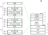
Fig. 1 is a cross-sectional view of a portion of an illustrative, but non-limiting, embodiment of a ill-nitride semiconductor LED device 10 according to the present disclosure.
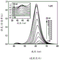
Fig. 2a is a graph illustrating the EL spectra of group III nitride semiconductor LED device 10 of fig. 1 emitting amber and red light with a current injection of 30 mA. The inset shows the EL spectra of the fig. 1 LED 10 in both amber and red with injection currents of 30 and 100mA in the short wavelength spectral region.
Fig. 2b shows that in the prior art: photoluminescence (PL) spectroscopy in U.S. patent application publication No. 20110237011a 1.
Fig. 2c shows the following prior art: current dependent EL spectra in app. phys.express 7, 071003 (2015).
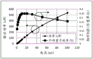
Fig. 3 is a graph illustrating output power and relative EQE (measurements performed in an on-wafer configuration) as a function of current for the red-emitting ill-nitride semiconductor LED device 10 of fig. 1.
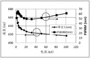
Fig. 4 is a graph illustrating peak wavelength shift and full width at half maximum (FWHM) as a function of current for the red-emitting ill-nitride semiconductor LED device 10 of fig. 1.
Fig. 5 is a graph illustrating output power and relative EQE as a function of current for the amber light emitting group III nitride semiconductor LED device 10 of fig. 1.
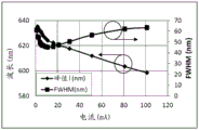
Fig. 6 is a graph illustrating peak wavelength shift and FWHM as a function of current for the amber light emitting group III nitride semiconductor LED device 10 of fig. 1.
Detailed Description
The present invention relates to long wavelength light emitting, group III nitride based semiconductor light emitting structures (such as LEDs and LDs) that are constructed by means of manipulating crystalline strain within the light emitting active region of the structure during an epitaxial growth process. The ill-nitride semiconductor light emitter structures of the present invention are described herein, and without limitation, within the context of LED device structures, however, one skilled in the art will recognize how to apply the methods of the present invention to the design of other ill-nitride semiconductor light emitters, including without limitation LDs.
The present invention discloses an innovative approach to constructing group III nitride based light emitting structures (such as LEDs or LDs) that do not suffer from excessive phase separation and are thus capable of emitting amber to red light with high spectral purity. Additional advantages and other features of the invention will be set forth in the description which follows and in part will become apparent to those having ordinary skill in the art upon examination of the following or may be learned from practice of the invention. Numerous advantages may be realized and attained as particularly pointed out in the claims hereinafter of any application claiming priority to this application.
According to one embodiment of the present invention, in a group III nitride semiconductor Light Emitting Diode (LED) structure, a first cladding layer is formed ofnA type group III nitride semiconductor layer. The light-emitting active region comprising indium in a layer comprising a group III nitridenA mold coat is formed thereon.pType AlGaN is formed on a light emission active region serving as an Electron Blocking Layer (EBL). Then, secondpA type III-nitride cladding layer is formed on the AlGaN layer.
According to further embodiments of the present invention, the light emitting region of a group III-nitride light emitter includes multiple sets of Multiple Quantum Wells (MQWs) separated by one or more intermediate strain compensation layers (hereinafter referred to as ISCLs) to minimize crystalline strain. The plurality of MQW sets and/or ISCLs may be vertically stacked on a surface of the substrate, thereby forming a multi-layer stack of MQW sets on the substrate. The multilayer stack may include: a first set of MQWs comprising GaN/InGaN with a lower indium concentration, a second set of MQWs comprising GaN/InGaN with a medium indium concentration and higher than the indium concentration of the first set, and a third set of MQWs comprising GaN/InGaN with the highest indium concentration capable of emitting light at the desired amber to red wavelengths. The first two sets of MQWs are used to create a pre-strain effect on the above-described group III nitride semiconductor layer of the group III nitride light emitting structure. However, herein, more than two MQW sets with variable indium concentration may be used to generate an equivalent pre-strain effect to that of the two MQW sets presented as a non-limiting example in this disclosure. In addition, an AlGaN layer is inserted as an Intermediate Strain Compensation Layer (ISCL) to minimize the total strain in the light emission region. By combining two (in this exemplary embodiment) or more pre-strained MQW GaN/InGaN collections with AlGaN ISCLs separating these collections, the emission wavelength of a group III nitride LED can be extended to amber and red regions with high spectral purity and high output power.
In a preferred embodiment of the present invention, the light emitting region of the group III nitride light emitting structure of the present invention includes: one or more group III nitride barrier layers and a lower indium multi-quantum well layer (first set of MQWs), a first ISCL comprising one or more group III nitride barrier layers and a medium indium multi-quantum well layer (second set of MQWs), a second ISCL, one or more barrier layers and a high indium content multi-quantum well layer (third set of MQWs) emitting amber to red light, and a top barrier layer, wherein each of the barrier layers consists essentially of GaN; each of the indium containing quantum well layers is composed of InGaN; and each of the ISCLs is composed of AlGaN.
In a first aspect of the invention, a multilayer group III-nitride semiconductor LED is disclosed that may include first, second, and third sets of layered MQW sets. The first set may include a first indium concentration. The second set may include a second indium concentration that is greater than the first indium concentration. The third set may include a third indium concentration that is greater than the second indium concentration. At least one of the first and second sets may beConfigured to act as a pre-strained layer. A first intermediate strain compensation layer may be provided and may be made of Al arranged between the first and second setsxGa1-xN (0<x is less than or equal to 1). A second intermediate strain compensation layer may be provided and may be made of Al arranged between the second and third setsxGa1-xN (0<x is less than or equal to 1). The first and second intermediate strain compensation layers may be disposed between two barrier layers, and the third set may be configured to emit light in the amber to red visible range having wavelengths ranging from about 600nm to about 660 nm.
In a second aspect of the invention, the first indium concentration may be less than about 17%.
In a third aspect of the invention, the second indium concentration may be greater than about 20%.
In a fourth aspect of the invention, the third indium concentration may be greater than about 30% and may be configured to emit amber to red light having a wavelength ranging from about 600nm to about 660 nm.
In a fifth aspect of the invention, at least one of the intermediate strain compensating layers may comprise AlxGa1-xN, wherein the value of x is greater than 0 and less than or equal to 1.
In a sixth aspect of the invention, the Al concentration in at least one of the intermediate strain compensating layers may vary, and the first intermediate strain compensating layer may comprise a higher Al concentration than the second intermediate strain compensating layer.
In a seventh aspect of the invention, at least one of the barrier layers may be composed of GaN, and at least one of the set may be composed of InGaN, and at least one of the intermediate strain compensation layers may be composed of AlxGa1-xN (0<x is less than or equal to 1).
In an eighth aspect of the present invention, there is disclosed a method for manufacturing a group III nitride semiconductor LED emitting amber to red light, comprising the steps of: defining a first barrier layer, defining a first set of MQW sets including a first indium concentration on the first barrier layerDefining a second barrier layer on the first set, the second barrier layer being defined by AlxGa1-xN (0<x ≦ 1), defining a third barrier layer on the first intermediate strain compensation layer, defining a second set of MQW sets on the third barrier layer comprising a second indium concentration greater than the first indium concentration, defining a fourth barrier layer on the second set, defining a second set of MQW sets on the fourth barrier layer, the second set of MQW sets comprising a second indium concentration greater than the first indium concentration, the fourth barrier layer comprising AlxGa1-xN (0<x ≦ 1), a fifth barrier layer defined on the second intermediate strain compensation layer, and a third set of MQW sets comprising a third indium concentration greater than the second indium concentration, the third indium concentration configured to emit light having a wavelength ranging from about 600nm to about 660 nm.
In a ninth aspect of the invention, at least one of the barrier layers made by the method may be composed of GaN, at least one of the sets may be composed of InGaN, the first intermediate strain compensation layer may include a higher Al concentration than the second intermediate strain compensation layer, the first set may include an indium concentration of not greater than about 17%, the second set may include an indium concentration greater than about 20%, and the third set may include an indium concentration greater than about 30% for emitting amber to red light.
The present invention provides an innovative LED device and method for fabricating a group III nitride solid state light emitting structure (such as an LED or LD) that emits amber to red wavelength light. The group III nitride solid state light emitter is epitaxially grown by using the method of the present invention, and thus amber and red wavelength light emission exhibiting high output power and high spectral purity is uniquely achieved without disturbing the phase separation of the prior art group III nitride light emission structure at long wavelengths.
The group III nitride semiconductor amber to red wavelength light emitters of the present invention are described herein within the context of the LED device structure illustrated in fig. 1 as illustrative exemplary embodiments of the present invention. FIG. 1 shows amber color according to the present inventionTo a cross-sectional view of a portion of an illustrative embodiment of a red group III-nitride LED 10. The amber to red group III-nitride LED device 10 may be fabricated by conventional epitaxial methods, such as Metal Organic Vapor Phase Epitaxy (MOVPE), also known as Metal Organic Chemical Vapor Deposition (MOCVD). As shown in fig. 1, an approximately 2 μm GaN buffer layer 2 is grown on a substrate 1, such as a sapphire substrate, with a nucleation layer (not shown) interposed therebetween. Of approximately 3 μm thickness doped with SinThe type GaN cladding layer 3 is grown on the GaN buffer layer 2. Illustrative embodiments of amber to red group III-nitride LEDs 10 may be grown epitaxially in a polar, semi-polar or non-polar crystal orientation by using a suitable substrate 1 crystal orientation.
Referring to fig. 1, the III-nitride LED structure includes a light emitting region or a Multiple Quantum Well (MQW) active region 4 included in a LEDnAn indium-containing group III nitride semiconductor layer grown on the type GaN layer 3. As illustrated in fig. 1, the active region 4 may include a bottom 4 having a curved surfaceAMQW ensemble to top MQW ensemble 4HThree types of MQW sets of increasing indium concentration. Each MQW set comprises one or more 2-3nm thick (depending on crystal orientation, it may be thicker) InGaN quantum well layers (4)A2, ..., 4E2, ..., 4H2...) and one or more barrier layers (4) consisting essentially of GaN and having a thickness of 5-20nmA1, ..., 4B, 4E1, ..., 4F, 4H1, ..., 4I) They are alternately stacked on top of each other with each InGaN quantum well layer sandwiched between two barrier layers. Accordingly, as shown in FIG. 1, MQW set 4A、4EAnd 4HMay be stacked vertically to produce a multi-layer stack of MQW sets 4. Group III nitride based barrier layer (4)A1, ..., 4B, 4E1, ..., 4F, 4H1, ..., 4I) Additional amounts of indium and/or aluminum may be included as needed to adjust their respective quantum well layers (4)A2, ..., 4E2, ..., 4H2...) is used. For the first MQW set 4AAnd a second set of MQWs 4EOf indium (2)The concentration is preferably in the range of 7-13% and 20-25%; respectively in the illustrated example. First two MQW sets 4AAnd 4EGeneration for the top MQW set 4HThe top MQW set 4, theHIndium concentrations of greater than 30% as preferred for amber to red light emission may be included.
In one embodiment of the present invention, the top MQW set 4 of the group III-nitride amber-to-red light-emitting structure of FIG. 1 is carefully controlledHHigh indium content quantum well layer (4)H2A.) high indium concentration without inducing phase separation. In this embodiment, the lower two MQW sets 4 with progressively higher indium concentrations are introducedAAnd 4ECreating a pre-strain effect on the barrier layer, thus facilitating the uppermost MQW set 4HHigh indium uptake in the inner. It is emphasized that including only one or even two MQW sets with low indium concentrations within a group III nitride light emitting structure may not produce a fully functional group III nitride semiconductor LED that emits in the amber to red region with high spectral purity and high output power. Thus, according to another embodiment of the present invention, and as shown in FIG. 1, an Intermediate Strain Compensating Layer (ISCL) 4CAnd 4GInterposed between every two successive MQW sets.
ISCL is sandwiched between the barrier layers of every two successive MQW sets, and is preferably made of AlxGa1-xN (0<x is less than or equal to 1), the AlxGa1-xN (0<x ≦ 1) varying Al concentration for the alloy, x being in the range of about 17% to about 25%. ISCL 4CAnd 4GThe thickness and Al concentration in (b) are preferably different. In one embodiment of the invention, the lower ISCL 4CThe Al concentration x in (1) can be higher than the upper ISCL 4GIn order to prevent layer cracking and to avoid excessive series resistance of the LED device 10 due to those layers. In another embodiment of the present invention, the lower ISCL 4CThe Al concentration x in (1) can be lower than the upper ISCL 4GMedium Al concentration so as to suppress the two lower indium concentration MQW sets 4AAnd 4EMedium carrier injection, which is beneficial to promote the top MQW set 4 toward high indium concentrationHThereby increasing the top MQW set 4HAnd thus reducing the full width at half maximum (FWHM) of the amber to red light emission of the group III nitride semiconductor light emitters of the present invention. Typically, the Al concentration varies with ISCL, although alternatively, the Al concentration in a separate intermediate strain compensation layer may vary within the intermediate strain compensation layer, in discrete steps (graded) within the layer, or as a continuous change in the respective layer.
Those skilled in the art will recognize that the ISCL 4 is selected using the previously mentioned methods of the present invention to depend on the target performance parameters for amber to red light emission of a group III nitride semiconductor light emitterCAnd 4GThe most suitable thickness and Al concentration in (c).
Referring back to FIG. 1, overlying MQW active region 4 of LED apparatus 10 ispLayer of type, thepThe type layers accordingly have a combined thickness of about 200nm and comprise a Mg-doped AlGaN Electron Blocking Layer (EBL) 5, a Mg-doped GaN cladding layer 6 and a Mg-doped GaN contact layer 7.pThe atomic concentration of Mg in the type AlGaN and GaN cladding layers is preferably from 1E19 cm-3To 1E20 cm-3In the range of (1).pThe Mg atom concentration in the type GaN contact layer is preferably, for example, 1E21 cm-3In the range of (1).
As in the prior art group III nitride light emitters, the group III nitride semiconductor amber to red light emitting device of the present invention is formed by: an ohmic contact metal stack is first deposited on the top side p-GaN layer 7 of the epitaxially processed wafer to form a p-side electrode 8, then a side trench is etched to expose the n-GaN layer 3, and then an ohmic contact metal stack is deposited within the etched trench to form an n-side electrode 9. The epitaxially processed wafer is then diced to form individual LED chips, each substantially having the cross-section illustrated in fig. 1, which are then packaged and wire bonded to respective p-and n-electrodes to form the LED device of the present inventionAnd (4) preparing. For the purpose of laboratory testing, it is known to use,pside electrodes (or ohmic contact metal stacks) 8, for example, and indium balls (for simplicity in rapid testing) are formed on the substratepOn the type GaN contact layer 7.
In addition, one side portion of the device 10 extends frompThe GaN contact layer 7 is etched tonPart of the type GaN cladding layer 3. Then, the user can use the device to perform the operation,nside electrodes (or ohmic contact metal stacks) 9, such as indium balls (for simplicity in rapid testing), are formed on the substratenOn the exposed portion of the type GaN cladding layer.
Passing through the positive electrodepSide electrodes 8 tonUnder current injection by the side electrode 9, visible light is emitted from the active region 4 through electron and hole recombination processes. Epitaxially grown group III-nitride semiconductor LED device 10 according to the method of the present invention is preferably configured such that only the top MQW set 4HLight is emitted, while the bottom two MQW sets 4AAnd 4EMainly acting as a pre-strained layer. With emission in the amber to red (amber-red) visible region at a current injection of about 30mA of 1mm2The group III nitride semiconductor LED device 10 of the region emits strong amber-red emission.
Fig. 2a is a graph illustrating a typical EL spectrum for the amber-red LED 10 of fig. 1 driven at about 30 mA. The inset shows the EL spectra of the exemplary embodiments of the invention of fig. 1, both amber and red, of group III-nitride LED 10 injecting currents at 30 and 100mA in the short wavelength spectral region. As seen in the inset of fig. 2(a), there are no additional peaks at shorter wavelength regions, even at higher drive currents of 100mA, indicating no phase separation in the inventive LED. In contrast, as shown in fig. 2b and 2c, which illustrate the performance of prior art LEDs, additional emission peaks (~ 440 nm) and a much wider FWHM emission due to phase separation were easily observed in prior art LEDs, U.S. patent application 20110237011a1 and app. phys.express 7, 071003 (2015), respectively.
Fig. 3 through 6 illustrate the performance of amber-red group III-nitride light emitter 10 of the present invention; fig. 3 and 4 illustrate the performance of one exemplary embodiment of the present invention whereby the device 10 active region 4 is designed for red (-625 nm) light emission (-45% indium concentration), while fig. 5 and 6 illustrate the performance of another exemplary embodiment of the present invention where the device 10 active region structure is designed for amber (-615 nm) light emission (-40% indium concentration).
Fig. 3 is a graph illustrating the measured current dependence of output power and relative EQE for a red-emitting ill-nitride LED device 10 for the present invention having its active region 4 designed to peak with red (-625 nm) light emission. All measurements were performed in a test configuration on a wafer with indium balls as respectivepSide andnboth side electrodes 8 and 9. The illustrated tests were performed without using special surface treatment and/or cooling units. Light is collected by an integrating sphere positioned below the LED 10, so not all light is collected. As shown in fig. 3, the output power increases with the applied current, following the power rules as observed in other group III nitride semiconductor-based LEDs. At 30mA, the output power of the red group III nitride semiconductor LED 10 reaches approximately 211 μ W. The relative EQE of the red group III nitride semiconductor LED 10 peaks at about 11mA by about 35% and then starts to monotonically decrease with increasing current. At 100mA, the relative EQE is reduced by approximately 26% compared to the peak. The true mechanism for EQE reduction with increasing current is still not well understood in the LED design community. There are basically two explanations for this phenomenon: (1) auger (Auger) recombination; and (2) electron leakage due to insufficient hole transport, are beyond the scope of this disclosure.
Fig. 4 is a graph illustrating an example of the measured emission peak wavelength shift and FWHM versus current for the red group III-nitride LED 10 of fig. 1. The emission peak wavelength shows a blue shift with increasing injection current. This behavior is characteristic of carrier shielding by piezoelectric fields in group III nitride based semiconductor LEDs. The band filling effect is also another cause of the blue shift. Emission peak wavelength at the wavelength of the emission peak due to strong band fillingShifted at low current but gradually saturated to 617nm at 100 mA. At 30mA, the emission peak wavelength was 625nm (red), and the FWHM was for a wavelength of 1mm2The devices of the region reached a minimum of 49nm at the same current level. To applicants' knowledge, this illustrates the best red emission performance from the group III nitride light emitters achieved to date.
Fig. 5 is a graph illustrating the current dependence of the output power and relative EQE of the group III nitride semiconductor LED device 10 of fig. 1 of the present invention having its active region 4 designed to peak with amber light emission. In a similar behavior to that of the red group III nitride semiconductor LED of the previous exemplary embodiment, for a semiconductor LED having a thickness of 1mm2The relative EQE of the area, amber group III nitride semiconductor LED, peaked to 45% at about 9mA and dropped to about 33% at 100 mA. The measured output power for the amber group III nitride LED was approximately 266 μ W at 30 mA.
Fig. 6 is a graph illustrating an example of measured changes in emission peak wavelength and FWHM with applied current for the amber group III nitride semiconductor LED 10 of fig. 1. Following a similar trend as for red group III nitride LEDs, the wavelength shifts at low currents but gradually saturates to 599nm at 100 mA. At 30mA, the peak wavelength was 617nm (amber) with a FWHM of 54 nm.
As described in the foregoing paragraphs, the group III nitride semiconductor LED emitting amber to red light with high output power and high spectral purity according to the present invention can be easily manufactured by careful control of material strain. The epitaxial growth method is compatible with the technique used to obtain group III-V compound semiconductors. Suitable epitaxial deposition techniques for use in practicing the present disclosure include, but are not limited to, MOVPE, Molecular Beam Epitaxy (MBE), and Hydride Vapor Phase Epitaxy (HVPE). The group III nitride based semiconductor layer may be formed, for example, from AlxGayIn1-x-yN, wherein x is more than or equal to 0 and less than or equal to 1 and y is more than or equal to 0 and less than or equal to 1. The planar orientation of the substrate 1 may becPlanar, semi-polar, and non-polar crystalline planes.
Furthermore, the LED device 10 according to the present disclosure can be easily constructed by utilizing conventional III-V compound semiconductor manufacturing methods and techniques.
While the foregoing disclosure has been described by way of example, it is to be understood that the disclosure is not so limited. It is intended to cover a wide range of modifications and similar arrangements. Modifications of the features or components of the present disclosure may be made without departing from the core concepts of the present disclosure. As a result, the scope of the disclosure is not limited by the foregoing description, but is only limited by the appended claims as set forth herein.
Claims (19)
1. A group III nitride semiconductor LED comprising:
a plurality of multiple quantum well sets stacked on a substrate, the plurality of multiple quantum well sets comprising first, second, and top multiple quantum well sets, each multiple quantum well set comprising one or more quantum well layers;
the first set of multiple quantum wells is adjacent to the substrate and has a low indium concentration;
each multiple quantum well set above the first multiple quantum well set has a gradually increasing indium concentration;
the top multi-quantum well set has a highest indium concentration selected to emit light in the amber to red visible spectral region; and is
Adjacent multiple quantum well set is covered with AlxGa1-xN (0<x is less than or equal to 1) separation of intermediate strain compensation layers, each AlxGa1-xN (0<x is less than or equal to 1) the intermediate strain compensation layer is arranged on the corresponding AlxGa1-xN (0<x ≦ 1) having barrier layers above and below the intermediate strain compensation layer to reduce the total strain in the top multiple quantum well set,
wherein Al isxGa1-xN (0<x ≦ 1) the Al concentration in the intermediate strain compensating layer is varied, wherein the Al closest to the substrate isxGa1-xN (0<x is less than or equal to 1) the intermediate strain compensation layer has higher Al content than other AlxGa1-xN (0<x is less than or equal to 1) higher Al of intermediate strain compensation layerAnd (4) concentration.
2. The group III nitride semiconductor LED according to claim 1, further comprising:
a barrier layer under the first set of multiple quantum wells;
an electron blocking layer over the top multiple quantum well set;
a capping layer over the electron blocking layer; and
a contact layer over the cladding layer.
3. The ill-nitride semiconductor LED according to claim 1, wherein the first, second and top multiple quantum well sets generate a pre-strain effect.
4. The group III nitride semiconductor LED according to claim 1, wherein the first multi-quantum well set having a low indium concentration includes one or more multi-quantum well layers having an indium concentration of not more than 17%.
5. The group III nitride semiconductor LED of claim 1, wherein a set of multiple quantum wells between the first set of multiple quantum wells and the top set of multiple quantum wells comprises one or more multiple quantum well layers having an indium concentration greater than 20%.
6. The group III nitride semiconductor LED of claim 1, wherein the top set of multiple quantum wells comprises one or more multiple quantum well layers having an indium concentration greater than 30%.
7. The group III nitride semiconductor LED according to claim 1, wherein AlxGa1-xN (0<x ≦ 1) the Al concentration in at least one of the intermediate strain compensating layers varies in discrete steps or in a continuous variation within the layer.
8. The group III nitride semiconductor LED according to claim 1, wherein Al is contained in the corresponding alloyxGa1-xN (0<x is less than or equal to 1) above the intermediate strain compensation layer andeach of the underlying barrier layers is composed of GaN, and each of the quantum well layers of the multiple quantum well set is composed of InGaN.
9. A method of forming a group III nitride semiconductor LED, comprising:
forming an active region having a set of multiple quantum well layers on a substrate by:
forming a set of first multiple quantum well layers having an indium concentration on a substrate;
forming a set of at least two additional MQWs on the set of first MQWs, forming Al on the previous set of MQWs before the formation of each additional set of MQWsxGa1-xN (0<x is less than or equal to 1) intermediate strain compensation layer, so that the first Al is formedxGa1-xN (0<x is less than or equal to 1) intermediate strain compensation layer and second AlxGa1-xN (0<x is less than or equal to 1) an intermediate strain compensation layer;
the set of at least two additional multiple quantum well layers has a higher indium concentration than the set of first multiple quantum well layers,
first Al closest to the substratexGa1-xN (0<x is less than or equal to 1) the intermediate strain compensation layer contains more than the second AlxGa1-xN (0<x is less than or equal to 1) higher Al concentration of the intermediate strain compensation layer.
10. The method of claim 9 wherein the indium concentration of the set of top multi-quantum well layers is selected for emission of light in the amber to red visible spectral region.
11. The method of claim 9 wherein the number of sets of multi-quantum well layers is at least 3, comprising a set of second multi-quantum well layers formed on the set of first multi-quantum well layers and a set of third multi-quantum well layers formed on the set of second multi-quantum well layers, wherein the set of third multi-quantum well layers has a higher indium concentration than the set of second multi-quantum well layers, the method further comprising:
at each AlxGa1-xN (0<x ≦ 1) forming barrier layers above and below the intermediate strain compensation layer, and wherein each of the barrier layers is comprised of GaN and each of the multiple quantum well layers is comprised of InGaN;
the set of first multi-quantum well layers has an indium concentration of no greater than 17%, the set of second multi-quantum well layers has an indium concentration greater than 20%, and the set of top multi-quantum well layers has an indium concentration greater than 30%.
12. A multilayer group III nitride semiconductor LED comprising:
a set of first, second and third multi-quantum well layers;
the set of first multi-quantum well layers has a first indium concentration;
the set of second multi-quantum well layers has a second indium concentration greater than the first indium concentration;
the set of third multi-quantum well layers has a third indium concentration greater than the second indium concentration;
al arranged between the sets of first and second multiple quantum well layersxGa1-xN (0<x is less than or equal to 1);
al arranged between the sets of second and third MQW layersxGa1-xN (0<x is less than or equal to 1);
first and second intermediate strain compensation layers are each disposed between the two barrier layers; and is
The set of third multi-quantum well layers is configured to emit light having a peak emission with a wavelength ranging from approximately 600nm to approximately 660nm,
wherein Al in at least one of the intermediate strain compensating layersxGa1-xN (0<x ≦ 1) the composition is varied, and the first intermediate strain compensating layer comprises a higher Al concentration than the second intermediate strain compensating layer.
13. The multilayer ill-nitride semiconductor LED of claim 12, wherein the first indium concentration is less than approximately 17%.
14. The multilayer ill-nitride semiconductor LED of claim 12, wherein the second indium concentration is greater than approximately 20%.
15. The multilayer group III nitride semiconductor LED of claim 12, wherein the third indium concentration is greater than approximately 30% and is selected such that the set of third multi-quantum well layers emits light in the amber to red visible spectral region.
16. The multilayer group III nitride semiconductor LED according to claim 12, wherein AlxGa1-xN (0<x ≦ 1) the Al concentration in at least one of the intermediate strain compensating layers varies in discrete steps or in a continuous variation within the layer.
17. The multi-layer group III nitride semiconductor LED of claim 12, wherein at least one of the barrier layers is comprised of GaN, and wherein at least one of the multiple quantum well layers in one of the sets of multiple quantum well layers is comprised of InGaN.
18. A method of manufacturing a group III nitride semiconductor LED that emits light in the amber to red visible region of the spectrum, comprising:
defining a first barrier layer;
defining a set of first multi-quantum well layers comprising a first indium concentration on a first barrier layer;
defining a second barrier layer on the set of first multi-quantum well layers;
defining Al on the second barrier layerxGa1-xN (0<x is less than or equal to 1);
defining a third barrier layer on the first intermediate strain compensation layer;
defining a set of second multi-quantum well layers on the third barrier layer, the set of second multi-quantum well layers including a second indium concentration greater than the first indium concentration;
defining a fourth barrier layer on the set of second multi-quantum well layers;
defining Al on the fourth barrier layerxGa1-xN (0<x is less than or equal to 1);
defining a fifth barrier layer on the second intermediate strain compensating layer; and
defining a set of third multi-quantum well layers comprising a third indium concentration greater than the second indium concentration, the third indium concentration configured to emit light having a peak emission at a wavelength ranging from approximately 600nm to approximately 660nm,
wherein the first intermediate strain compensating layer comprises a higher concentration of Al than the second intermediate strain compensating layer.
19. The method of claim 18 wherein at least one of the barrier layers is comprised of GaN, and wherein at least one of the multiple quantum well layers in one of the sets of multiple quantum well layers is comprised of InGaN, and wherein the first set of multiple quantum well layers includes an indium concentration of no greater than approximately 17%, and wherein the second set of multiple quantum well layers includes an indium concentration greater than approximately 20%, and wherein the third set of multiple quantum well layers includes an indium concentration greater than approximately 30%.
Applications Claiming Priority (5)
| Application Number | Priority Date | Filing Date | Title |
|---|---|---|---|
| US201562239122P | 2015-10-08 | 2015-10-08 | |
| US62/239122 | 2015-10-08 | ||
| US15/287384 | 2016-10-06 | ||
| US15/287,384 US10396240B2 (en) | 2015-10-08 | 2016-10-06 | III-nitride semiconductor light emitting device having amber-to-red light emission (>600 nm) and a method for making same |
| PCT/US2016/056157 WO2017062889A1 (en) | 2015-10-08 | 2016-10-07 | III-NITRIDE SEMICONDUCTOR LIGHT EMITTING DEVICE HAVING AMBER-TO-RED LIGHT EMISSION (>600 nm) AND A METHOD FOR MAKING SAME |
Publications (2)
| Publication Number | Publication Date |
|---|---|
| CN108292693A CN108292693A (en) | 2018-07-17 |
| CN108292693B true CN108292693B (en) | 2021-10-22 |
Family
ID=57184854
Family Applications (1)
| Application Number | Title | Priority Date | Filing Date |
|---|---|---|---|
| CN201680072137.5A Expired - Fee Related CN108292693B (en) | 2015-10-08 | 2016-10-07 | Group III nitride semiconductor light emitting devices with amber to red (> 600 nm) light emission and methods for making the same |
Country Status (8)
| Country | Link |
|---|---|
| US (1) | US10396240B2 (en) |
| EP (1) | EP3360168B1 (en) |
| JP (2) | JP2018531514A (en) |
| KR (1) | KR20180067590A (en) |
| CN (1) | CN108292693B (en) |
| HK (1) | HK1258318A1 (en) |
| TW (1) | TWI775729B (en) |
| WO (1) | WO2017062889A1 (en) |
Families Citing this family (11)
| Publication number | Priority date | Publication date | Assignee | Title |
|---|---|---|---|---|
| CN114640024A (en) | 2015-06-05 | 2022-06-17 | 奥斯坦多科技公司 | Light emitting structure with selective carrier injection into multiple active layers |
| US11056434B2 (en) * | 2017-01-26 | 2021-07-06 | Epistar Corporation | Semiconductor device having specified p-type dopant concentration profile |
| US10971652B2 (en) * | 2017-01-26 | 2021-04-06 | Epistar Corporation | Semiconductor device comprising electron blocking layers |
| WO2019130753A1 (en) * | 2017-12-27 | 2019-07-04 | オリンパス株式会社 | Light source device |
| FR3089686B1 (en) * | 2018-12-11 | 2020-11-13 | Aledia | Optoelectronic device comprising pixels emitting three colors |
| US11404473B2 (en) | 2019-12-23 | 2022-08-02 | Lumileds Llc | III-nitride multi-wavelength LED arrays |
| US11923398B2 (en) | 2019-12-23 | 2024-03-05 | Lumileds Llc | III-nitride multi-wavelength LED arrays |
| WO2021226121A1 (en) * | 2020-05-04 | 2021-11-11 | Raxium, Inc. | Light emitting diodes with aluminum-containing layers integrated therein and associated methods |
| JP2023526488A (en) | 2020-05-19 | 2023-06-21 | グーグル エルエルシー | Combining strain management layers for light emitting devices |
| US11264535B1 (en) * | 2020-08-12 | 2022-03-01 | Jyh-Chia Chen | Pixel device and display using a monolithic blue/green LED combined with red luminescence materials |
| US11631786B2 (en) | 2020-11-12 | 2023-04-18 | Lumileds Llc | III-nitride multi-wavelength LED arrays with etch stop layer |
Family Cites Families (80)
| Publication number | Priority date | Publication date | Assignee | Title |
|---|---|---|---|---|
| US4839899A (en) | 1988-03-09 | 1989-06-13 | Xerox Corporation | Wavelength tuning of multiple quantum well (MQW) heterostructure lasers |
| JPH04350988A (en) * | 1991-05-29 | 1992-12-04 | Nec Kansai Ltd | Light-emitting element of quantum well structure |
| US5422898A (en) | 1993-10-29 | 1995-06-06 | International Business Machines Corporation | Tapered Fabry-Perot multi-wavelength optical source |
| US5386428A (en) | 1993-11-02 | 1995-01-31 | Xerox Corporation | Stacked active region laser array for multicolor emissions |
| JP2682474B2 (en) * | 1993-11-26 | 1997-11-26 | 日本電気株式会社 | Semiconductor laser device |
| US5737353A (en) | 1993-11-26 | 1998-04-07 | Nec Corporation | Multiquantum-well semiconductor laser |
| JPH08316588A (en) | 1995-05-23 | 1996-11-29 | Furukawa Electric Co Ltd:The | Semiconductor optical element having strained quantum well structure |
| US5684309A (en) * | 1996-07-11 | 1997-11-04 | North Carolina State University | Stacked quantum well aluminum indium gallium nitride light emitting diodes |
| JPH1187773A (en) * | 1997-09-08 | 1999-03-30 | Toshiba Corp | Light emitting element |
| TW412889B (en) | 1997-09-24 | 2000-11-21 | Nippon Oxygen Co Ltd | Semiconductor laser |
| WO2000058999A2 (en) | 1999-03-26 | 2000-10-05 | Matsushita Electric Industrial Co., Ltd. | Semiconductor structures having a strain compensated layer and method of fabrication |
| US7202506B1 (en) | 1999-11-19 | 2007-04-10 | Cree, Inc. | Multi element, multi color solid state LED/laser |
| NL1015860C2 (en) * | 2000-08-02 | 2002-02-05 | Wavin Bv | Methods and devices for manufacturing a tube of biaxially oriented thermoplastic plastic material with an integral sleeve. |
| US6469358B1 (en) | 2000-09-21 | 2002-10-22 | Lockheed Martin Corporation | Three color quantum well focal plane arrays |
| JP2002176198A (en) * | 2000-12-11 | 2002-06-21 | Mitsubishi Cable Ind Ltd | Multi-wavelength light emitting element |
| KR100906760B1 (en) | 2001-03-28 | 2009-07-09 | 니치아 카가쿠 고교 가부시키가이샤 | Nitride semiconductor device |
| JP2004146498A (en) | 2002-10-23 | 2004-05-20 | Stanley Electric Co Ltd | Semiconductor light-emitting device |
| CA2427559A1 (en) | 2002-05-15 | 2003-11-15 | Sumitomo Electric Industries, Ltd. | White color light emitting device |
| US7058105B2 (en) | 2002-10-17 | 2006-06-06 | Samsung Electro-Mechanics Co., Ltd. | Semiconductor optoelectronic device |
| US6927412B2 (en) | 2002-11-21 | 2005-08-09 | Ricoh Company, Ltd. | Semiconductor light emitter |
| JP4571372B2 (en) * | 2002-11-27 | 2010-10-27 | ローム株式会社 | Semiconductor light emitting device |
| US20040161006A1 (en) * | 2003-02-18 | 2004-08-19 | Ying-Lan Chang | Method and apparatus for improving wavelength stability for InGaAsN devices |
| US6919584B2 (en) | 2003-06-19 | 2005-07-19 | Harvatek Corporation | White light source |
| KR100482511B1 (en) | 2004-02-05 | 2005-04-14 | 에피밸리 주식회사 | Ⅲ-Nitride compound semiconductor light emitting device |
| US7323721B2 (en) | 2004-09-09 | 2008-01-29 | Blue Photonics Inc. | Monolithic multi-color, multi-quantum well semiconductor LED |
| US8148713B2 (en) | 2008-04-04 | 2012-04-03 | The Regents Of The University Of California | Method for fabrication of semipolar (Al, In, Ga, B)N based light emitting diodes |
| KR100649749B1 (en) * | 2005-10-25 | 2006-11-27 | 삼성전기주식회사 | Nitride semiconductor light emitting device |
| KR100665364B1 (en) * | 2005-12-28 | 2007-01-09 | 삼성전기주식회사 | Nitride semiconductor light emitting device |
| KR20070080696A (en) | 2006-02-08 | 2007-08-13 | 삼성전자주식회사 | Nitride based semiconductor laser diode |
| KR100774200B1 (en) | 2006-04-13 | 2007-11-08 | 엘지전자 주식회사 | Organic Electroluminescence Device and method for fabricating the same |
| US7593436B2 (en) | 2006-06-16 | 2009-09-22 | Vi Systems Gmbh | Electrooptically Bragg-reflector stopband-tunable optoelectronic device for high-speed data transfer |
| KR20080035865A (en) * | 2006-10-20 | 2008-04-24 | 삼성전자주식회사 | Semiconductor light emitting device |
| TWI338382B (en) | 2006-11-29 | 2011-03-01 | Univ Nat Taiwan | Method and structure for manufacturing long-wavelength light-emitting diode using prestrain effect |
| KR100862497B1 (en) | 2006-12-26 | 2008-10-08 | 삼성전기주식회사 | Nitride semiconductor device |
| JP2008235606A (en) | 2007-03-20 | 2008-10-02 | Sony Corp | Semiconductor light-emitting element, method for manufacturing semiconductor light-emitting element, backlight, display unit, electronic equipment, and light-emitting device |
| US7649195B2 (en) * | 2007-06-12 | 2010-01-19 | Seoul Opto Device Co., Ltd. | Light emitting diode having active region of multi quantum well structure |
| US7623560B2 (en) | 2007-09-27 | 2009-11-24 | Ostendo Technologies, Inc. | Quantum photonic imagers and methods of fabrication thereof |
| GB2456756A (en) | 2008-01-16 | 2009-07-29 | Sharp Kk | AlInGaN Light-Emitting devices |
| JP4720834B2 (en) | 2008-02-25 | 2011-07-13 | 住友電気工業株式会社 | Group III nitride semiconductor laser |
| JP2009224370A (en) * | 2008-03-13 | 2009-10-01 | Rohm Co Ltd | Nitride semiconductor device |
| JP2011517099A (en) * | 2008-04-04 | 2011-05-26 | ザ リージェンツ オブ ザ ユニバーシティ オブ カリフォルニア | MOCVD growth technology for planar semipolar (Al, In, Ga, B) N-based light-emitting diodes |
| TW200950162A (en) * | 2008-04-04 | 2009-12-01 | Univ California | Method for fabrication of semipolar (Al, In, Ga, B)N based light emitting diodes |
| US20100006873A1 (en) | 2008-06-25 | 2010-01-14 | Soraa, Inc. | HIGHLY POLARIZED WHITE LIGHT SOURCE BY COMBINING BLUE LED ON SEMIPOLAR OR NONPOLAR GaN WITH YELLOW LED ON SEMIPOLAR OR NONPOLAR GaN |
| US20110133158A1 (en) | 2008-08-19 | 2011-06-09 | Lattice Power (Jiangxi) Corporation | Method for fabricating ingan-based multi-quantum well layers |
| JP5394717B2 (en) * | 2008-12-15 | 2014-01-22 | 日本オクラロ株式会社 | Manufacturing method of nitride semiconductor optical device |
| JP4775455B2 (en) * | 2009-02-17 | 2011-09-21 | 住友電気工業株式会社 | Group III nitride semiconductor laser and method of fabricating group III nitride semiconductor laser |
| US9153790B2 (en) | 2009-05-22 | 2015-10-06 | Idemitsu Kosan Co., Ltd. | Organic electroluminescent device |
| US8296624B2 (en) * | 2009-06-30 | 2012-10-23 | Comcast Cable Communications, Llc | Variable interleave data transmission |
| CN102484047A (en) * | 2009-08-21 | 2012-05-30 | 加利福尼亚大学董事会 | Semipolar nitride-based devices on partially or fully relaxed alloys with misfit dislocations at the heterointerface |
| US8314429B1 (en) | 2009-09-14 | 2012-11-20 | Soraa, Inc. | Multi color active regions for white light emitting diode |
| US9484197B2 (en) | 2009-10-23 | 2016-11-01 | The Royal Institution For The Advancement Of Learning/Mcgill University | Lateral growth semiconductor method and devices |
| KR100993085B1 (en) * | 2009-12-07 | 2010-11-08 | 엘지이노텍 주식회사 | Light emitting device, light emitting device package, and lighting unit |
| CN102668138B (en) | 2009-12-21 | 2015-06-10 | 株式会社东芝 | Nitride semiconductor light-emitting element and method for manufacturing same |
| TWI508621B (en) | 2010-02-03 | 2015-11-11 | Innolux Corp | System for displaying images |
| US20110188528A1 (en) | 2010-02-04 | 2011-08-04 | Ostendo Technologies, Inc. | High Injection Efficiency Polar and Non-Polar III-Nitrides Light Emitters |
| JP4940317B2 (en) * | 2010-02-25 | 2012-05-30 | 株式会社東芝 | Semiconductor light emitting device and manufacturing method thereof |
| US8451877B1 (en) | 2010-03-23 | 2013-05-28 | Sandia Corporation | High efficiency III-nitride light-emitting diodes |
| US20110237011A1 (en) | 2010-03-29 | 2011-09-29 | Nanjing University | Method for Forming a GaN-Based Quantum-Well LED with Red Light |
| JP5533744B2 (en) * | 2010-03-31 | 2014-06-25 | 豊田合成株式会社 | Group III nitride semiconductor light emitting device |
| US20120000866A1 (en) * | 2010-06-30 | 2012-01-05 | Randal Huszczo | Glass Storage and Transport Rack with Pivoting Arms |
| JP5372045B2 (en) | 2011-02-25 | 2013-12-18 | 株式会社東芝 | Semiconductor light emitting device |
| JP5737111B2 (en) * | 2011-03-30 | 2015-06-17 | 豊田合成株式会社 | Group III nitride semiconductor light emitting device |
| US8686397B2 (en) | 2011-06-10 | 2014-04-01 | The Regents Of The University Of California | Low droop light emitting diode structure on gallium nitride semipolar substrates |
| US8927958B2 (en) * | 2011-07-12 | 2015-01-06 | Epistar Corporation | Light-emitting element with multiple light-emitting stacked layers |
| GB201112792D0 (en) * | 2011-07-26 | 2011-09-07 | Smith Michael | A ratchet buckle use for the tightening of straps |
| US9070613B2 (en) | 2011-09-07 | 2015-06-30 | Lg Innotek Co., Ltd. | Light emitting device |
| US8772791B2 (en) | 2011-09-29 | 2014-07-08 | Epistar Corporation | Light-emitting device |
| KR20130078345A (en) | 2011-12-30 | 2013-07-10 | 일진엘이디(주) | Nitride based light emitting device with excellent light efficiency using strain buffer layer |
| JP6136284B2 (en) | 2012-03-13 | 2017-05-31 | 株式会社リコー | Semiconductor laminate and surface emitting laser element |
| US9124062B2 (en) * | 2012-03-22 | 2015-09-01 | Palo Alto Research Center Incorporated | Optically pumped surface emitting lasers incorporating high reflectivity/bandwidth limited reflector |
| KR101936305B1 (en) | 2012-09-24 | 2019-01-08 | 엘지이노텍 주식회사 | Light emitting device |
| JP2014067893A (en) * | 2012-09-26 | 2014-04-17 | Toyoda Gosei Co Ltd | Group iii nitride semiconductor light-emitting element |
| US9978904B2 (en) * | 2012-10-16 | 2018-05-22 | Soraa, Inc. | Indium gallium nitride light emitting devices |
| US8890114B2 (en) | 2012-10-16 | 2014-11-18 | Epistar Corporation | Light-emitting device |
| US9847444B2 (en) | 2012-11-06 | 2017-12-19 | Canon Kabushiki Kaisha | Photonic device and optical coherence tomography apparatus including the photonic device as light source |
| DE102013108782B4 (en) * | 2012-11-21 | 2024-05-08 | Epistar Corp. | Light emitting device with multiple light emitting stack layers |
| US8941111B2 (en) | 2012-12-21 | 2015-01-27 | Invensas Corporation | Non-crystalline inorganic light emitting diode |
| US11502219B2 (en) | 2013-03-14 | 2022-11-15 | The Royal Institution For The Advancement Of Learning/Mcgill University | Methods and devices for solid state nanowire devices |
| US10839734B2 (en) | 2013-12-23 | 2020-11-17 | Universal Display Corporation | OLED color tuning by driving mode variation |
| CN114640024A (en) | 2015-06-05 | 2022-06-17 | 奥斯坦多科技公司 | Light emitting structure with selective carrier injection into multiple active layers |
-
2016
- 2016-10-06 US US15/287,384 patent/US10396240B2/en not_active Expired - Fee Related
- 2016-10-07 JP JP2018517812A patent/JP2018531514A/en active Pending
- 2016-10-07 TW TW105132658A patent/TWI775729B/en active
- 2016-10-07 EP EP16784685.6A patent/EP3360168B1/en active Active
- 2016-10-07 WO PCT/US2016/056157 patent/WO2017062889A1/en active Application Filing
- 2016-10-07 CN CN201680072137.5A patent/CN108292693B/en not_active Expired - Fee Related
- 2016-10-07 KR KR1020187013012A patent/KR20180067590A/en not_active Application Discontinuation
-
2019
- 2019-01-16 HK HK19100686.8A patent/HK1258318A1/en unknown
-
2022
- 2022-03-09 JP JP2022036024A patent/JP2022071179A/en active Pending
Also Published As
| Publication number | Publication date |
|---|---|
| TW201735390A (en) | 2017-10-01 |
| JP2018531514A (en) | 2018-10-25 |
| CN108292693A (en) | 2018-07-17 |
| US10396240B2 (en) | 2019-08-27 |
| JP2022071179A (en) | 2022-05-13 |
| KR20180067590A (en) | 2018-06-20 |
| US20170104128A1 (en) | 2017-04-13 |
| HK1258318A1 (en) | 2019-11-08 |
| EP3360168A1 (en) | 2018-08-15 |
| WO2017062889A1 (en) | 2017-04-13 |
| TWI775729B (en) | 2022-09-01 |
| EP3360168B1 (en) | 2021-09-29 |
Similar Documents
| Publication | Publication Date | Title |
|---|---|---|
| CN108292693B (en) | Group III nitride semiconductor light emitting devices with amber to red (> 600 nm) light emission and methods for making the same | |
| JP2018531514A6 (en) | Group III nitride semiconductor light emitting device having amber to red emission (> 600 nm) and method for making the same | |
| US9035324B2 (en) | Light emitting device | |
| KR100956579B1 (en) | Semiconductor and method of semiconductor fabrication | |
| US20100288999A1 (en) | Group iii nitride semiconductor light-emitting device | |
| WO2009041237A1 (en) | Iii nitride semiconductor light emitting element | |
| JP6111250B2 (en) | Optoelectronic parts | |
| JP6457784B2 (en) | Semiconductor light emitting device | |
| US10186671B2 (en) | Semiconductor light-emitting element | |
| KR20170080598A (en) | Semiconductor light-emitting element | |
| JP6433248B2 (en) | Semiconductor light emitting device | |
| JP2016513878A (en) | Monolithic light emitting device | |
| KR101485690B1 (en) | Semiconductor light emitting device and method for manufacturing the same | |
| JP2023536362A (en) | LED device and method for manufacturing LED device | |
| CN112802869A (en) | White light LED with adjustable single-chip integrated nitride light-emitting wavelength and preparation method thereof | |
| JP2009105423A (en) | Group iii nitride semiconductor light emitting device | |
| TWI420696B (en) | Light-emitting device and the manufacturing method thereof |
Legal Events
| Date | Code | Title | Description |
|---|---|---|---|
| PB01 | Publication | ||
| PB01 | Publication | ||
| SE01 | Entry into force of request for substantive examination | ||
| SE01 | Entry into force of request for substantive examination | ||
| REG | Reference to a national code |
Ref country code: HK Ref legal event code: DE Ref document number: 1258318 Country of ref document: HK |
|
| GR01 | Patent grant | ||
| GR01 | Patent grant | ||
| CF01 | Termination of patent right due to non-payment of annual fee | ||
| CF01 | Termination of patent right due to non-payment of annual fee |
Granted publication date: 20211022 |