JP2018525792A - LED array on the board - Google Patents
LED array on the board Download PDFInfo
- Publication number
- JP2018525792A JP2018525792A JP2018509556A JP2018509556A JP2018525792A JP 2018525792 A JP2018525792 A JP 2018525792A JP 2018509556 A JP2018509556 A JP 2018509556A JP 2018509556 A JP2018509556 A JP 2018509556A JP 2018525792 A JP2018525792 A JP 2018525792A
- Authority
- JP
- Japan
- Prior art keywords
- lighting
- carrier board
- board
- windings
- carrier
- Prior art date
- Legal status (The legal status is an assumption and is not a legal conclusion. Google has not performed a legal analysis and makes no representation as to the accuracy of the status listed.)
- Pending
Links
Images


Classifications
-
- F—MECHANICAL ENGINEERING; LIGHTING; HEATING; WEAPONS; BLASTING
- F21—LIGHTING
- F21S—NON-PORTABLE LIGHTING DEVICES; SYSTEMS THEREOF; VEHICLE LIGHTING DEVICES SPECIALLY ADAPTED FOR VEHICLE EXTERIORS
- F21S4/00—Lighting devices or systems using a string or strip of light sources
- F21S4/10—Lighting devices or systems using a string or strip of light sources with light sources attached to loose electric cables, e.g. Christmas tree lights
-
- F—MECHANICAL ENGINEERING; LIGHTING; HEATING; WEAPONS; BLASTING
- F21—LIGHTING
- F21S—NON-PORTABLE LIGHTING DEVICES; SYSTEMS THEREOF; VEHICLE LIGHTING DEVICES SPECIALLY ADAPTED FOR VEHICLE EXTERIORS
- F21S4/00—Lighting devices or systems using a string or strip of light sources
- F21S4/20—Lighting devices or systems using a string or strip of light sources with light sources held by or within elongate supports
- F21S4/28—Lighting devices or systems using a string or strip of light sources with light sources held by or within elongate supports rigid, e.g. LED bars
-
- F—MECHANICAL ENGINEERING; LIGHTING; HEATING; WEAPONS; BLASTING
- F21—LIGHTING
- F21V—FUNCTIONAL FEATURES OR DETAILS OF LIGHTING DEVICES OR SYSTEMS THEREOF; STRUCTURAL COMBINATIONS OF LIGHTING DEVICES WITH OTHER ARTICLES, NOT OTHERWISE PROVIDED FOR
- F21V29/00—Protecting lighting devices from thermal damage; Cooling or heating arrangements specially adapted for lighting devices or systems
- F21V29/50—Cooling arrangements
- F21V29/502—Cooling arrangements characterised by the adaptation for cooling of specific components
- F21V29/503—Cooling arrangements characterised by the adaptation for cooling of specific components of light sources
-
- F—MECHANICAL ENGINEERING; LIGHTING; HEATING; WEAPONS; BLASTING
- F21—LIGHTING
- F21V—FUNCTIONAL FEATURES OR DETAILS OF LIGHTING DEVICES OR SYSTEMS THEREOF; STRUCTURAL COMBINATIONS OF LIGHTING DEVICES WITH OTHER ARTICLES, NOT OTHERWISE PROVIDED FOR
- F21V29/00—Protecting lighting devices from thermal damage; Cooling or heating arrangements specially adapted for lighting devices or systems
- F21V29/50—Cooling arrangements
- F21V29/70—Cooling arrangements characterised by passive heat-dissipating elements, e.g. heat-sinks
-
- H—ELECTRICITY
- H05—ELECTRIC TECHNIQUES NOT OTHERWISE PROVIDED FOR
- H05K—PRINTED CIRCUITS; CASINGS OR CONSTRUCTIONAL DETAILS OF ELECTRIC APPARATUS; MANUFACTURE OF ASSEMBLAGES OF ELECTRICAL COMPONENTS
- H05K3/00—Apparatus or processes for manufacturing printed circuits
- H05K3/0011—Working of insulating substrates or insulating layers
- H05K3/0044—Mechanical working of the substrate, e.g. drilling or punching
- H05K3/0052—Depaneling, i.e. dividing a panel into circuit boards; Working of the edges of circuit boards
-
- F—MECHANICAL ENGINEERING; LIGHTING; HEATING; WEAPONS; BLASTING
- F21—LIGHTING
- F21Y—INDEXING SCHEME ASSOCIATED WITH SUBCLASSES F21K, F21L, F21S and F21V, RELATING TO THE FORM OR THE KIND OF THE LIGHT SOURCES OR OF THE COLOUR OF THE LIGHT EMITTED
- F21Y2103/00—Elongate light sources, e.g. fluorescent tubes
- F21Y2103/10—Elongate light sources, e.g. fluorescent tubes comprising a linear array of point-like light-generating elements
-
- F—MECHANICAL ENGINEERING; LIGHTING; HEATING; WEAPONS; BLASTING
- F21—LIGHTING
- F21Y—INDEXING SCHEME ASSOCIATED WITH SUBCLASSES F21K, F21L, F21S and F21V, RELATING TO THE FORM OR THE KIND OF THE LIGHT SOURCES OR OF THE COLOUR OF THE LIGHT EMITTED
- F21Y2103/00—Elongate light sources, e.g. fluorescent tubes
- F21Y2103/20—Elongate light sources, e.g. fluorescent tubes of polygonal shape, e.g. square or rectangular
-
- F—MECHANICAL ENGINEERING; LIGHTING; HEATING; WEAPONS; BLASTING
- F21—LIGHTING
- F21Y—INDEXING SCHEME ASSOCIATED WITH SUBCLASSES F21K, F21L, F21S and F21V, RELATING TO THE FORM OR THE KIND OF THE LIGHT SOURCES OR OF THE COLOUR OF THE LIGHT EMITTED
- F21Y2103/00—Elongate light sources, e.g. fluorescent tubes
- F21Y2103/30—Elongate light sources, e.g. fluorescent tubes curved
-
- F—MECHANICAL ENGINEERING; LIGHTING; HEATING; WEAPONS; BLASTING
- F21—LIGHTING
- F21Y—INDEXING SCHEME ASSOCIATED WITH SUBCLASSES F21K, F21L, F21S and F21V, RELATING TO THE FORM OR THE KIND OF THE LIGHT SOURCES OR OF THE COLOUR OF THE LIGHT EMITTED
- F21Y2115/00—Light-generating elements of semiconductor light sources
- F21Y2115/10—Light-emitting diodes [LED]
-
- H—ELECTRICITY
- H05—ELECTRIC TECHNIQUES NOT OTHERWISE PROVIDED FOR
- H05K—PRINTED CIRCUITS; CASINGS OR CONSTRUCTIONAL DETAILS OF ELECTRIC APPARATUS; MANUFACTURE OF ASSEMBLAGES OF ELECTRICAL COMPONENTS
- H05K2201/00—Indexing scheme relating to printed circuits covered by H05K1/00
- H05K2201/09—Shape and layout
- H05K2201/09009—Substrate related
- H05K2201/09027—Non-rectangular flat PCB, e.g. circular
-
- H—ELECTRICITY
- H05—ELECTRIC TECHNIQUES NOT OTHERWISE PROVIDED FOR
- H05K—PRINTED CIRCUITS; CASINGS OR CONSTRUCTIONAL DETAILS OF ELECTRIC APPARATUS; MANUFACTURE OF ASSEMBLAGES OF ELECTRICAL COMPONENTS
- H05K2201/00—Indexing scheme relating to printed circuits covered by H05K1/00
- H05K2201/09—Shape and layout
- H05K2201/09009—Substrate related
- H05K2201/09127—PCB or component having an integral separable or breakable part
-
- H—ELECTRICITY
- H05—ELECTRIC TECHNIQUES NOT OTHERWISE PROVIDED FOR
- H05K—PRINTED CIRCUITS; CASINGS OR CONSTRUCTIONAL DETAILS OF ELECTRIC APPARATUS; MANUFACTURE OF ASSEMBLAGES OF ELECTRICAL COMPONENTS
- H05K2201/00—Indexing scheme relating to printed circuits covered by H05K1/00
- H05K2201/09—Shape and layout
- H05K2201/09818—Shape or layout details not covered by a single group of H05K2201/09009 - H05K2201/09809
- H05K2201/09918—Optically detected marks used for aligning tool relative to the PCB, e.g. for mounting of components
-
- H—ELECTRICITY
- H05—ELECTRIC TECHNIQUES NOT OTHERWISE PROVIDED FOR
- H05K—PRINTED CIRCUITS; CASINGS OR CONSTRUCTIONAL DETAILS OF ELECTRIC APPARATUS; MANUFACTURE OF ASSEMBLAGES OF ELECTRICAL COMPONENTS
- H05K2201/00—Indexing scheme relating to printed circuits covered by H05K1/00
- H05K2201/09—Shape and layout
- H05K2201/09818—Shape or layout details not covered by a single group of H05K2201/09009 - H05K2201/09809
- H05K2201/09972—Partitioned, e.g. portions of a PCB dedicated to different functions; Boundary lines therefore; Portions of a PCB being processed separately or differently
-
- H—ELECTRICITY
- H05—ELECTRIC TECHNIQUES NOT OTHERWISE PROVIDED FOR
- H05K—PRINTED CIRCUITS; CASINGS OR CONSTRUCTIONAL DETAILS OF ELECTRIC APPARATUS; MANUFACTURE OF ASSEMBLAGES OF ELECTRICAL COMPONENTS
- H05K2201/00—Indexing scheme relating to printed circuits covered by H05K1/00
- H05K2201/10—Details of components or other objects attached to or integrated in a printed circuit board
- H05K2201/10007—Types of components
- H05K2201/10106—Light emitting diode [LED]
-
- H—ELECTRICITY
- H05—ELECTRIC TECHNIQUES NOT OTHERWISE PROVIDED FOR
- H05K—PRINTED CIRCUITS; CASINGS OR CONSTRUCTIONAL DETAILS OF ELECTRIC APPARATUS; MANUFACTURE OF ASSEMBLAGES OF ELECTRICAL COMPONENTS
- H05K3/00—Apparatus or processes for manufacturing printed circuits
- H05K3/0097—Processing two or more printed circuits simultaneously, e.g. made from a common substrate, or temporarily stacked circuit boards
Landscapes
- Engineering & Computer Science (AREA)
- General Engineering & Computer Science (AREA)
- Manufacturing & Machinery (AREA)
- Microelectronics & Electronic Packaging (AREA)
- Non-Portable Lighting Devices Or Systems Thereof (AREA)
- Electroluminescent Light Sources (AREA)
- Planar Illumination Modules (AREA)
- Fastening Of Light Sources Or Lamp Holders (AREA)
- Arrangement Of Elements, Cooling, Sealing, Or The Like Of Lighting Devices (AREA)
- Structures For Mounting Electric Components On Printed Circuit Boards (AREA)
- Structure Of Printed Boards (AREA)
Abstract
照明デバイスは、キャリアボード、及びキャリアボードに設けられた照明要素のアレイを有する。キャリアボードは、概してスパイラルの形状を持ち、該キャリアボードは、1つ以上の同一の他のキャリアボードと、巻線が互いに交互配置されるようにテセレーションされ得る。これは、複数のキャリアボードが、殆ど又は全く材料を無駄にすることなく単一の基板から形成されることを可能にする。異なるデザインは、2つ、4つ又はさらに多くの異なる同一のキャリアボードの形状が、一緒にテセレーションすることを可能にする。 The lighting device has a carrier board and an array of lighting elements provided on the carrier board. The carrier board has a generally spiral shape, and the carrier board can be tessellated with one or more identical other carrier boards such that the windings are interleaved with each other. This allows multiple carrier boards to be formed from a single substrate with little or no material wastage. Different designs allow two, four or more different identical carrier board shapes to be tessellated together.
Description
本発明は、照明デバイスに関し、とりわけ、プリント回路基板等のボードに設けられたLED等の照明要素のアレイを有する照明デバイスに関する。 The present invention relates to lighting devices, and more particularly to lighting devices having an array of lighting elements such as LEDs provided on a board such as a printed circuit board.
一般照明では、低ピーク輝度を提供し、斯くして、快適な低グレア照明を提供するために、大面積光源がよく使用される。LEDアレイを有するLED照明器具では、小型で明るい個々のLEDが、大面積光源を作り出すために、プリント回路基板等の大面積ボード上に比較的離れて配置される必要がある。通常、斯かる光源は、個々のLEDを隠すために拡散板又は箔と組み合わされる。 In general lighting, large area light sources are often used to provide low peak brightness and thus provide comfortable low glare lighting. In LED lighting fixtures with LED arrays, small and bright individual LEDs need to be placed relatively far apart on a large area board such as a printed circuit board in order to create a large area light source. Usually, such a light source is combined with a diffuser or foil to hide individual LEDs.
LED技術のトレンドは、LEDの小型化、効率の向上(斯くして、熱散逸 (thermal dissipation)の低下)及びコストの削減である。結果として、LEDは、所要の熱的及び機械的設計の制約を満たすために、LEDあたりより少ないPCB領域を必要とする。PCBコストもまた、総コスト(すなわち部品表(BOM))のより重要な部分になっている。 LED technology trends are LED miniaturization, increased efficiency (thus lower thermal dissipation) and cost reduction. As a result, LEDs require less PCB area per LED to meet the required thermal and mechanical design constraints. PCB cost has also become a more important part of the total cost (ie bill of materials (BOM)).
このトレンドの結果として開発された1つのデザインは、いわゆるEパネルである。斯かるパネルでは、長方形のPCB領域が、全領域を依然カバーする2つの互いにかみ合った(E字状の)部分にボードを切断することによって二分される。 One design developed as a result of this trend is the so-called E-panel. In such a panel, the rectangular PCB area is bisected by cutting the board into two interlocking (E-shaped) portions that still cover the entire area.
これにより、2つの同一の基板が、材料を無駄にすることなく単一のボードから形成されることができる。また、完全な領域を部分的にしか覆わないが、(直線状セグメント等の)複数のセグメントを結合する必要のない形状を形成することができる。LEDの規則的な配列は、E字状のボードに位置付けられ得る。 This allows two identical substrates to be formed from a single board without wasting material. Also, it is possible to form a shape that only partially covers the complete area but does not require the joining of multiple segments (such as straight segments). A regular array of LEDs can be located on an E-shaped board.
より高い効率及びより低いコストのトレンドが進むにつれて、Eパネルは、未使用のPCB領域のために依然としてコストペナルティを受ける。Eパネルのデザインでは、例えば、当初のボードを3つ以上の同一部分に切断することはできない。したがって、Eパネルのデザインはそれ程汎用性がない。それゆえ、未使用のPCB領域を減らすPCBボードの代替デザインの必要性がある。 As the trend of higher efficiency and lower cost progresses, E-panels still incur cost penalties for unused PCB areas. In the E-panel design, for example, the original board cannot be cut into three or more identical parts. Therefore, the design of the E panel is not so versatile. Therefore, there is a need for alternative PCB board designs that reduce unused PCB space.
本発明は、特許請求の範囲により規定される。 The invention is defined by the claims.
本発明の一態様による例によれば、キャリアボード、及び前記キャリアボードに設けられた照明要素のアレイを有する照明デバイスであって、前記キャリアボードは、該キャリアボードが、1つ以上の同一形状又は類似形状の他のキャリアボードと、巻線が互いに交互配置されるようにテセレーションされることを可能にするような、少なくとも2つの収束巻線を備えるコイル形状を持つ、照明デバイスが提供される。前記巻線は、複数の直線状セクションを有し、コイルに沿った隣接する前記セクション間の角度は90°であり、隣接する巻線間の垂直方向の間隔は一定である。前記直線状セクションは、狭い幅と広い幅とで変化する幅を持ち、前記照明要素は、広い幅を持つ部分に位置し、前記照明要素のアレイは、正方形又は長方形グリッドを形成する。 According to an example according to an aspect of the invention, a lighting device comprising a carrier board and an array of lighting elements provided on the carrier board, the carrier board comprising one or more identical shapes. Or a lighting device is provided having a coil shape with at least two converging windings to allow other carrier boards of similar shape and the windings to be tessellated to interleave with each other. The The winding has a plurality of straight sections, the angle between adjacent sections along the coil is 90 °, and the vertical spacing between adjacent windings is constant. The linear section has a width that varies between a narrow width and a wide width, the lighting elements are located in a portion having a wide width, and the array of lighting elements forms a square or rectangular grid.
「類似」及び「同様」という用語は、テセレーションされることができるボードが互いにスカラーストレッチされたバージョンであってもよいという点で数学的な意味において用いられる(すなわち、トポロジー的に類似している)。これは、例えば、同一のキャリアボード形状がテセレーションされ、そして、テセレーションされた構造がストレッチされ、個々の構成要素に分離される場合である。好ましくは、テセレーションされるキャリアボードは、全て同じ製品のサンプルを形成するように同一である。 The terms “similar” and “similar” are used in a mathematical sense in that boards that can be tessellated may be scalar stretched versions of each other (ie, topologically similar). ) This is the case, for example, when the same carrier board shape is tessellated and the tessellated structure is stretched and separated into individual components. Preferably, the carrier boards to be tessellated are identical so as to form all samples of the same product.
コイル形状は、複数のキャリアボードが単一のテセレーションされたデザインとして初期的に製造されることができる一方、該キャリアボードの面積を減らすことを可能にする。 The coil shape allows multiple carrier boards to be initially manufactured as a single tessellated design, while reducing the area of the carrier board.
キャリアボードは、例えば、プリント回路基板を含んでもよいが、適切な熱的及び機械的安定性並びに電気的相互接続を提供する任意の基板が用いられてもよい。 The carrier board may include, for example, a printed circuit board, but any board that provides appropriate thermal and mechanical stability and electrical interconnection may be used.
これは、金属基板上に印刷された電気トレース等の印刷されたエレクトロニクスだけでなく、従来のPCB(マルチコアPCB又は単一コアPCB及び異なる材料のもの)を含む。 This includes not only printed electronics such as electrical traces printed on metal substrates, but also conventional PCBs (multicore PCBs or single core PCBs and of different materials).
コイル形状は、収束巻線、すなわち、中心点に向かって収束する巻線を持つ。コイル巻線は、直線状セクションから形成される、すなわち、概ね多角形である。 The coil shape has convergent windings, that is, windings that converge toward the center point. The coil winding is formed from straight sections, i.e. is generally polygonal.
巻線は、隣接する巻線間の垂直方向の間隔が一定であるように、コイルに沿って隣接するセクション間の90度の角度で直線状セクションを含む。これは、正方形(又は長方形)のスパイラル形状を有する構造を規定する。巻線間の一定の間隔は、当該間隔がアルキメデスの渦巻の正方形/長方形のバージョンとして述べられ得る形状を形成することを意味する。一定の間隔は、直線状セクションの幅の倍数に対応する。倍数は、最初のものと一緒にテセレーションされることができる他の同じ形状の数である。 The winding includes straight sections at a 90 degree angle between adjacent sections along the coil so that the vertical spacing between adjacent windings is constant. This defines a structure having a square (or rectangular) spiral shape. A constant spacing between the windings means that the spacing forms a shape that can be described as a square / rectangular version of the Archimedean spiral. The constant spacing corresponds to a multiple of the width of the straight section. A multiple is the number of other identical shapes that can be tessellated with the first one.
キャリアボードは、互いに交互配置される巻線を有する1つの同一の他のキャリアボードとテセレーションされることができる。これら2つは、実質的に領域を一緒に満たすことができる。これは、2つの斯かるコイル形状が、ボード材料の最小限の無駄しかない又は無駄のないボードから形成され得ることを意味する。 The carrier board can be tessellated with one identical other carrier board having windings interleaved with each other. These two can substantially fill the area together. This means that two such coil shapes can be formed from a board with minimal or no waste of board material.
照明要素のアレイは、規則的な正方形又は長方形のグリッドを形成する。これは、Eパネルデザインの代替案を提供する。 The array of lighting elements forms a regular square or rectangular grid. This provides an alternative to E-panel design.
キャリアボードは、互いに交互配置される巻線を有する3つの同一の他のキャリアボードとテセレーションされることもできる。ここでも、これら4つは、実質的にボード領域を満たすことができる。これは、4つの斯かるコイル形状が、ボード材料の最小限の無駄しかない又は無駄のないボードから形成され得ることを意味する。 The carrier board can also be tessellated with three identical other carrier boards with windings interleaved with each other. Again, these four can substantially fill the board area. This means that four such coil shapes can be formed from a board with minimal or no waste of board material.
本発明による照明デバイスのデザインは、各々が照明要素の規則的な正方形又は長方形のグリッドを有するように、1つ以上の(例えば4つの)同一のコイル形状がテセレーションされ得ることを可能にする。これは、直線状セクションの幅が狭い幅と広い幅との間で変化し、照明要素が幅の広い部分に位置するためである。このようにして、1つの直線状セクションの幅の広い部分は、複数のコイルがテセレーションされる場合に、異なるコイルの側方に隣接する巻線の幅の狭い部分と噛み合う。 The design of the lighting device according to the invention allows one or more (eg four) identical coil shapes to be tessellated so that each has a regular square or rectangular grid of lighting elements. . This is because the width of the linear section varies between a narrow width and a wide width, and the lighting element is located in a wide portion. In this way, the wide portion of one straight section meshes with the narrow portion of the winding adjacent to the sides of the different coils when multiple coils are tessellated.
このデザインはまた、放熱が必要な各照明要素の周りの大きなキャリアボード領域と、相互接続部分における薄いキャリアボード領域とを提供し、ボード材料の使用がより効率的になる。 This design also provides a large carrier board area around each lighting element that needs to be dissipated and a thin carrier board area at the interconnect, making the use of board material more efficient.
幅の狭い部分は、へこみ(indent)により形成され、交互直線状セクション(alternate straight section)の一方の組についてのへこみは、内側縁にあり、交互直線状セクションの他方の組についてのへこみは、外側縁にある。これは、異なるコイル間の各90°の回転で、1つのコイルの直線状セクションに沿った幅の広い部分が、隣接するコイルの隣接する直線状セクションの幅の狭い部分と噛み合うことを意味する。 The narrow portion is formed by an indent, the dent for one set of alternate straight sections is at the inner edge, and the dent for the other set of alternating straight sections is On the outer edge. This means that with each 90 ° rotation between different coils, the wide portion along the straight section of one coil meshes with the narrow portion of the adjacent straight section of the adjacent coil. .
本発明の他の態様による例は、照明デバイスを製造する方法であって、キャリアボード上に照明要素のアレイを形成するステップ、キャリアボードを少なくとも2つの同一形状又は類似形状のセクションに分割するステップであって、各セクションの照明要素のアレイは、正方形又は長方形グリッドを形成する、ステップを有する方法であり、各セクションは、複数の収束巻線を備えるコイル形状を持ち、巻線は、分割前に互いに交互配置されていて、巻線は、複数の直線状セクションを有し、コイルに沿った隣接するセクション間の角度は90°であり、隣接する巻線間の垂直方向の間隔は一定であり、直線状セクションは、狭い幅と広い幅とで変化する幅を持ち、照明要素は、広い幅を持つ部分に位置する、方法を提供する。 An example according to another aspect of the invention is a method of manufacturing a lighting device, the step of forming an array of lighting elements on a carrier board, the step of dividing the carrier board into at least two sections of identical or similar shape Wherein the array of lighting elements in each section is a method having steps, forming a square or rectangular grid, each section having a coil shape with a plurality of converging windings, the windings being pre-split The windings have a plurality of straight sections, the angle between adjacent sections along the coil is 90 °, and the vertical spacing between adjacent windings is constant. Yes, the linear section has a width that varies between a narrow width and a wide width, and the lighting element provides a method that is located in a portion having a wide width.
このようにして、複数のボードが、はまり合う(tessellate together)同一の形状を分離することによって、単一の初期ボードから形成される。 In this way, multiple boards are formed from a single initial board by separating the same shape tessellate together.
狭い幅の部分は、へこみにより形成され、交互直線状セクションの一方の組についてのへこみは、内側縁にあり、交互直線状セクションの他方の組についてのへこみは、外側縁にあってもよい。 The narrow width portion is formed by a dent, the dent for one set of alternating linear sections may be at the inner edge, and the dent for the other set of alternating linear sections may be at the outer edge.
本発明のこれらの及び他の態様は、以下に述べられる実施形態を参照して明らかになり、詳述されるであろう。 These and other aspects of the invention will be apparent from and elucidated with reference to the embodiments described hereinafter.
ここで、本発明の例が、添付の図面を参照して詳細に述べられる。
本発明は、キャリアボード、及びキャリアボードに設けられた照明要素のアレイを有する照明デバイスを提供する。キャリアボードは、概してスパイラル(コイル状)の形状を持ち、該キャリアボードは、1つ以上の同一の他のキャリアボードと、巻線が互いに交互配置されるようにテセレーションされ得る。これは、複数のキャリアボードが、殆ど又は全く材料を無駄にすることなく単一の基板から形成されることを可能にする。異なるデザインは、2つ、4つ又はさらに多くの異なる同一のキャリアボードの形状が、一緒にテセレーションすることを可能にする。 The present invention provides a lighting device having a carrier board and an array of lighting elements provided on the carrier board. The carrier board has a generally spiral (coiled) shape, which can be tessellated with one or more identical other carrier boards and windings interleaved with each other. This allows multiple carrier boards to be formed from a single substrate with little or no material wastage. Different designs allow two, four or more different identical carrier board shapes to be tessellated together.
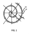
図1は、スパイラルの形態で形成される照明デバイスの第1の例を示す。照明デバイスは、キャリアボード10、及びキャリアボードに設けられた照明要素12のアレイを有する。
FIG. 1 shows a first example of a lighting device formed in the form of a spiral. The lighting device comprises a
本発明による全ての例において、キャリアボードは、複数の収束巻線を備えるコイル形状を持ち、キャリアボードは、巻線が互いに交互配置される1つ以上の同一の他のキャリアボードでテセレーションされることができる。 In all examples according to the invention, the carrier board has a coil shape with a plurality of converging windings, and the carrier board is tessellated with one or more other identical carrier boards in which the windings are interleaved with each other. Can.
図1の例は、曲線状のスパイラル、具体的にはアルキメデスの螺旋である。これは、巻線間の距離dが一定であるという特性を有する。また、これは、複数の斯かる螺旋がテセレーションされ得るという特性も有する。テセレーションされ得る数は、巻線ピッチ(すなわち、間隔dとトラックの幅wとの和)をトラックの幅で割ったもの、すなわち、
N =(w + d)/ w
に相当する。
The example of FIG. 1 is a curved spiral, specifically an Archimedean spiral. This has the property that the distance d between the windings is constant. It also has the property that a plurality of such spirals can be tessellated. The number that can be tessellated is the winding pitch (ie the sum of the spacing d and the track width w) divided by the track width, ie
N = (w + d) / w
It corresponds to.
これは、N個のスパイラル状のデザインが、ボードの単一の領域から形成され、その後、例えばフライス加工、パンチング又は他の切断技術によって別々の同一領域に分離されることを意味する。切断された製品において、切断ラインの厚さが、その比率をわずかに変えるであろう。 This means that N spiral designs are formed from a single area of the board and then separated into separate identical areas, for example by milling, punching or other cutting techniques. In the cut product, the thickness of the cutting line will change the ratio slightly.
スパイラル状のデザインは、幅と間隔を適切に選択することによって、任意の数のキャリアボードが規定されることを可能にする。各個別のボードは、熱的及び機械的サポート要件を満たす必要があり、さらに、照明要素12を収容するのに十分な幅を有する必要がある。必要とされる放熱が減るにつれて、キャリアボードの所要面積は減少し、幅wを減少させることができる。これは、より多くのキャリアボードが所与のエリアから形成されることを可能にし、コストを節約することができる。
The spiral design allows any number of carrier boards to be defined by appropriate selection of width and spacing. Each individual board must meet the thermal and mechanical support requirements and must have a width sufficient to accommodate the
照明要素はスパイラルパターンに従う。これは、照明要素が規則的な長方形又は六角形のグリッドとして配設され得ることを意味する。しかしながら、照明要素は、単位面積当たりの照明要素の密度が、ボードの領域にわたって実質的に一定であるように配設されることができる。例えば、照明要素は、スパイラルに沿って均等に、巻線ピッチ(w + d)又は巻線間隔(d)に等しいか又はほぼ等しい間隔(例えば、0.5d及び1.5(w + d )の間)で離間されてもよい。 The lighting elements follow a spiral pattern. This means that the lighting elements can be arranged as a regular rectangular or hexagonal grid. However, the lighting elements can be arranged such that the density of the lighting elements per unit area is substantially constant over the area of the board. For example, the lighting elements are equally spaced along the spiral, equal to or approximately equal to the winding pitch (w + d) or winding spacing (d) (eg, between 0.5d and 1.5 (w + d)) May be separated by
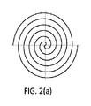
複数のスパイラルをテセレーションするために、隣接するスパイラル間の回転シフトが提供される。N個の同一のスパイラルの場合、隣接する交互配置されたスパイラル間の相対的な回転シフトは360/N°である。 In order to tessellate multiple spirals, a rotational shift between adjacent spirals is provided. For N identical spirals, the relative rotational shift between adjacent interleaved spirals is 360 / N °.
図2は、3つの可能な交互配置されるスパイラルパターンを示す。図2は、各スパイラルの形状を、トラックとしてではなく、単純にするため線で示している。 FIG. 2 shows three possible interleaved spiral patterns. FIG. 2 shows the shape of each spiral as a line for simplicity, not as a track.
図2(a)は、180°度回転シフトした2つの交互配置されるスパイラルを示す。 FIG. 2 (a) shows two alternating spirals that are 180 ° rotationally shifted.
図2(b)は、90°回転シフトした4つの交互配置されるスパイラルを示す。 FIG. 2 (b) shows four interleaved spirals shifted by 90 °.
図2(c)は、45°回転シフトした8つの交互配置されるスパイラルを示す。 FIG. 2 (c) shows eight interleaved spirals shifted by 45 °.
キャリアボードはプリント回路基板を含むが、適切な熱的及び機械的安定性並びに電気的相互接続を提供する任意の基板が用いられてもよい。 The carrier board includes a printed circuit board, but any board that provides adequate thermal and mechanical stability and electrical interconnection may be used.
これは、金属基板上に印刷された電気トレース等の印刷されたエレクトロニクスだけでなく、従来のPCB(マルチコアPCB又は単一コアPCB、及び異なる材料のもの)を含む。 This includes not only printed electronics such as electrical traces printed on metal substrates, but also conventional PCBs (multi-core or single-core PCBs, and of different materials).
プリント回路基板は一般にラミネート構造であり、ラミネートは、任意の基板成形が行われる前の連続シートとして最も容易に形成される。斯くして、任意のパターン化された形状を形成すると、PCBの損失(wastage)が生じる。スパイラルを交互配置することによって、PCBの全領域(又はほぼ全領域)がキャリアボードを作成するために用いられる。 The printed circuit board is generally a laminate structure, and the laminate is most easily formed as a continuous sheet before any substrate molding is performed. Thus, forming any patterned shape results in PCB wastage. By interleaving the spirals, the entire area (or almost the entire area) of the PCB is used to create the carrier board.
照明要素は、照明要素の駆動を可能にするため、導電性トラックによって互いに接続される。照明要素はすべて、直列、並列であってもよく、又は直列及び並列接続の組み合わせ、例えば、並列枝の組であって、各枝が一組の直列照明要素を担持してもよい。一例における接続端子(典型的には、アノード接続とカソード接続のみ)は、容易な電気接続を可能にするため、最も外側の巻線の端部に設けられる。それに代えて、接続は、接続点からスパイラルの端部まで用いられる電気的トラックの最大長を最小にするため、コイル形状に沿った中間位置にあってもよい。このようにして、スパイラルの長さ全体に沿った1つのトラックが、各々がスパイラルの長さの一部をカバーする2つのトラックに置換される。 The lighting elements are connected to each other by conductive tracks to allow driving of the lighting elements. All lighting elements may be in series, in parallel, or a combination of series and parallel connections, eg, a set of parallel branches, each branch carrying a set of series lighting elements. The connection terminals in one example (typically only the anode and cathode connections) are provided at the end of the outermost winding to allow easy electrical connection. Alternatively, the connection may be in an intermediate position along the coil shape to minimize the maximum length of the electrical track used from the connection point to the end of the spiral. In this way, one track along the entire length of the spiral is replaced with two tracks, each covering a portion of the length of the spiral.
スパイラル形状のキャリアボードを有する単一の照明デバイスが、照明製品に用いられてもよい。しかしながら、光出力を増加させるために、複数の照明デバイスが、単一の製品で用いられてもよい。したがって、単一のスパイラル状のデザインが、異なるタイプの照明製品に対してモジュール方式で用いられてもよい。一般に、完全数Nのスパイラルのサブセットが用いられる。N個のスパイラルがすべて製品に要求される場合、よりコスト効率が高いのは、単一のボードを提供すること(すなわち、切断及び分離プロセスを実行しないこと)である。しかしながら、これが製品範囲のほんの一部である場合、モジュラーアプローチを使用して製造することは依然としてより効率が高い可能性がある。N未満の任意の数について、複数の個別のスパイラルボードを使用することは、コスト効率が高い解決策である。 A single lighting device having a spiral shaped carrier board may be used in the lighting product. However, multiple lighting devices may be used in a single product to increase the light output. Thus, a single spiral design may be used in a modular fashion for different types of lighting products. In general, a subset of the full number N spirals is used. If all N spirals are required for a product, it is more cost effective to provide a single board (ie, not perform a cutting and separation process). However, if this is only a small part of the product range, it may still be more efficient to manufacture using a modular approach. Using multiple individual spiral boards for any number less than N is a cost effective solution.
このデザインは容易に修正され得る。例えば、照明要素の位置及びカバーされる全領域(overall area covered)は、各照明要素のためのキャリアボード領域の必要性が減少する場合、スパイラル幅wを減少させながら同じに保たれてもよい。したがって、同じ光学デザインのより多くのキャリアボードが、各処理済みの全面キャリアボード(each processed full area carrier board)から作製され得る。 This design can be easily modified. For example, the location of the lighting elements and the overall area covered may be kept the same while reducing the spiral width w if the need for a carrier board area for each lighting element is reduced. . Thus, more carrier boards of the same optical design can be made from each processed full area carrier board.
キャリアボードの外形は概して円形であるので、このデザインは、円形の製品にとってとりわけ興味深い。 This design is particularly interesting for circular products, since the carrier board profile is generally circular.
上述したように、スパイラル形状は、望まれる可能性がある、照明要素の規則的な長方形又は正方形のグリッドを与えない。 As mentioned above, the spiral shape does not provide a regular rectangular or square grid of lighting elements that may be desired.
図3は、照明デバイスの第2の例を示す。照明素子12が設けられるキャリアボード10は、ここでもコイル形状を有するが、滑らかなスパイラル(smooth spiral)ではなく、角度構造(angular structure)である。
FIG. 3 shows a second example of the lighting device. The
この例において、巻線は、コイルに沿った隣接するセクション間に90°の角度を有する直線状セクション10a、10b、10c、10dを含む。隣接する巻線間の垂直間隔dは、やはり一定である。したがって、この構造は、正方形(又は長方形)のスパイラル形状を有する。
In this example, the winding includes
巻線間の一定の間隔dは、アルキメデスの渦巻の正方形/長方形のバージョンとして述べられ得る形状を形成することを意味する。一定の間隔dは、直線状セクションの幅wの倍数に相当する。倍数は、最初のものと一緒にテセレーションされ得る他の同じ形状の数である。 A constant spacing d between the windings means forming a shape that can be described as a square / rectangular version of the Archimedean spiral. The constant distance d corresponds to a multiple of the width w of the straight section. A multiple is the number of other identical shapes that can be tessellated with the first.
図3は、他の同一の1つのコイル形状とテセレーションされることができるデザイン、すなわち、(切断線の厚さを無視して)N =(d + w)/ w = 2であることを示す。 Figure 3 shows that the design can be tessellated with other identical single coil shapes, ie N = (d + w) / w = 2 (ignoring the cutting line thickness) Show.
このデザインの利点は、照明要素12が規則的な正方形(又は長方形)のグリッドとして形成され得ることである。これは、全領域にわたる照明要素の均一な密度、したがって、均一な光出力を与える。
An advantage of this design is that the
図4は、キャリアボード材料を無駄にすることなく、長方形領域を満たすようにテセレーションされる2つのキャリアボードを示す。斯くして、2つの照明デバイスは、一緒に製造され、その後、製造プロセスの終わりに分離される。 FIG. 4 shows two carrier boards that are tessellated to fill a rectangular area without wasting carrier board material. Thus, the two lighting devices are manufactured together and then separated at the end of the manufacturing process.
キャリアボードの外形は概して正方形/長方形であるので、このデザインは、正方形又は長方形の製品にとってとりわけ興味深い。 This design is particularly interesting for square or rectangular products because the carrier board outline is generally square / rectangular.
しかしながら、同様の正方形のスパイラル形状は、N = 4となるようにコイルの幅wを小さくすることによって、4つのキャリアボードを形成するために用いられてもよい。 However, a similar square spiral shape may be used to form four carrier boards by reducing the coil width w such that N = 4.
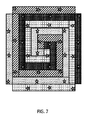
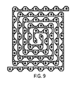
図5は、N = 4である照明デバイスの第3の例を示す。このデザインは、巻線が相互に交互配置されてやはり実質的に領域を満たすように、3つの同一の他のキャリアボードとテセレーションされることができる。これは、4つの斯かるコイル形状が、ボード材料の無駄を最小限にするか又は全く有さないボードから形成され得ることを意味する。 FIG. 5 shows a third example of a lighting device with N = 4. This design can be tessellated with three identical other carrier boards so that the windings are interleaved with each other and still substantially fill the area. This means that four such coil shapes can be formed from a board with minimal or no waste of board material.
図5の基本デザインにおいて、直線状セクションは、すべて一定の幅wである。 In the basic design of FIG. 5, the straight sections are all of a constant width w.
このデザインでは、照明要素をセクションの中央に配置することはできないが、規則的なグリッドを形成することができる。代わりに、照明要素のアレイは、照明要素の直線的な行及び列のグリッドを形成できるが、完全に規則的なグリッドは形成できない。グリッドは中央の規則性を失う。 With this design, the lighting elements cannot be placed in the center of the section, but can form a regular grid. Instead, an array of lighting elements can form a linear row and column grid of lighting elements, but not a perfectly regular grid. The grid loses its central regularity.
図6は、規則的なグリッドがコイル形状の上にどのようにしてフィットするのが最良であるかを示し、照明要素12がコイルトラックのエッジに沿って常にセンタリングされていることを示す。斯くして、この構造は容易に製造することができない。
FIG. 6 shows how a regular grid is best fit over the coil shape and shows that the
したがって、基本的な正方形のコイルデザインは、規則的なLEDグリッドが必要とされる場合、2つのキャリアボードを形成することしか可能にしない。 Thus, the basic square coil design only allows two carrier boards to be formed when a regular LED grid is required.
図5のデザインにおける光強度の変動は許容可能であろう。とりわけ、光強度の変動は、中央しか生じていない。光強度の変動は、異なる出力電力の照明要素を異なる場所に設けることにより補償されてもよい。 Variations in light intensity in the design of FIG. 5 would be acceptable. In particular, the fluctuation of the light intensity occurs only at the center. Variations in light intensity may be compensated by providing different output power illumination elements at different locations.
図7は、テセレーションされた図5の4つの同一の照明デバイスを示す。 FIG. 7 shows the four identical lighting devices of FIG. 5 being tessellated.
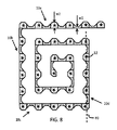
図8は、照明要素の規則的なグリッドを維持しながら4つの同一のコイル形状を形成することを可能にする照明デバイスの第4の例を示す。 FIG. 8 shows a fourth example of a lighting device that makes it possible to form four identical coil shapes while maintaining a regular grid of lighting elements.
一般に、このデザインは、図3及び図5のデザインと同じ全体形状、すなわち、正方形/長方形のコイル構造を持つ。 In general, this design has the same overall shape as the designs of FIGS. 3 and 5, ie, a square / rectangular coil structure.
しかしながら、直線状セクション10a、10b、10c、10dは、狭い幅w1と広い幅w2との間で変化する幅を有し、照明要素12は、幅の広い部分に配置される。直線状セクションは、これらが直線の軸方向に沿って延びるという意味において依然直線状である。
However, the
直線状セクションは、中心軸線80を有すると考えられてもよく(それらがこの軸に関して対称ではないにもかかわらず)、各直線状セクションは、狭い部分及び広い部分を有する。狭い部分は、中心軸80がセクションの領域の外側にあることを意味し、一方、広い部分は、中心軸がセクションの領域内にあることを意味する。このようにして、照明要素12は、中心軸80に沿って位置決めされることができる。このようにして、照明要素は、図6に示されるような様式で位置決めされることができる。
The straight sections may be considered to have a central axis 80 (even though they are not symmetric about this axis), and each straight section has a narrow portion and a wide portion. The narrow part means that the
1つの直線状セクションの広い部分は、複数のコイルがテセレーションされる場合、異なるコイルの側方に隣接する巻線の狭い部分と噛み合う。 The wide portion of one straight section meshes with the narrow portion of the winding adjacent to the sides of the different coils when multiple coils are tessellated.
各直線状セクションの一方の縁は直線状であり、他方の縁は輪郭のある縁(profiled edge)を形成する。幅の狭い部分は、輪郭のある縁に沿ったへこみにより形成されてもよく、交互直線状セクションの一方の組についてのへこみは内側縁にあり、交互直線状セクションの他方の組についてのへこみは外側縁にある。従って、一方の組の交互直線状セクションの直線状の縁は外側縁にあり、他方の組の交互直線状セクションの直線状の縁は内側縁にある。 One edge of each straight section is straight and the other edge forms a profiled edge. The narrow portion may be formed by a dent along the contoured edge, where the dent for one set of alternating linear sections is at the inner edge and the dent for the other set of alternating linear sections is On the outer edge. Thus, the straight edge of one set of alternating linear sections is at the outer edge and the straight edge of the other set of alternating straight sections is at the inner edge.
これは、テセレーションされた場合4つの異なるコイル間の各90°の回転で、1つのコイルの直線状セクションに沿った幅の広い部分が、隣接するコイルの隣接する直線状セクションの幅の狭い部分と噛み合うことを意味する。 This is because each 90 ° rotation between four different coils when tessellated causes the wide portion along the straight section of one coil to narrow the adjacent straight section of the adjacent coil. Means to mesh with the part.
図9は、互いに交互配置された図8の2つの同一の照明デバイスを示す。これは、モジュール式に、図8のデバイスの光出力フラックス(light output flux)を2倍にしたデバイスをもたらす。コイルは、照明要素の複合グリッドを均等に分布させるために(180°の回転シフトをもって)離間されている。 FIG. 9 shows the two identical lighting devices of FIG. 8 interleaved with each other. This results in a device that modularly doubles the light output flux of the device of FIG. The coils are spaced apart (with a 180 ° rotational shift) to evenly distribute the composite grid of lighting elements.
照明製品は、図8の1つ、2つ、3つ、又は4つすべての照明デバイスを用いてもよい。 The lighting product may use one, two, three, or all four lighting devices of FIG.
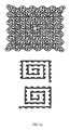
図10は、テセレーションされた図8の4つの同一の照明デバイスを示し、どのようにして4つの照明デバイスが製造されるかを示している。 FIG. 10 shows four identical lighting devices of FIG. 8 that have been tessellated and shows how four lighting devices are manufactured.
コイルの有限の幅は、それらが完全な点に収束しないことを意味する。この例において、中心にPCBボードの小さな星がある(これは、キャリアボードのいずれにも必要とされない)が、4つのコイルすべてが完全にテセレーションするようにコイル形状の最も内側の部分がデザインされることも等しく可能である。 The finite width of the coils means that they do not converge to a perfect point. In this example, there is a small star on the PCB board in the center (which is not required on any of the carrier boards), but the innermost part of the coil shape is designed so that all four coils are fully tessellated. It is equally possible to be done.
4つのテセレーションされたコイルの外形は概して正方形であり、正方形のボードからの損失はほとんどない。 The outline of the four tessellated coils is generally square, with little loss from the square board.
図示のデザインは、1つの軸に沿って伸ばされ、それによりすべての正方形のプロファイルを長方形のプロファイルに変換することも可能である。この場合、個々のボードはもはや同一ではないが、同一の機能を実行する。この場合、個々のボードは、互いのスカラー伸長バージョン(scalar stretched version)である。 The illustrated design can be stretched along one axis, thereby converting all square profiles to rectangular profiles. In this case, the individual boards are no longer identical but perform the same function. In this case, the individual boards are mutually scalar stretched versions.
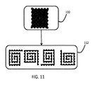
照明デバイスの製造方法が、図11に示される。この方法は、
ステップ110における、キャリアボード上に照明要素のアレイを形成するステップ、及び
ステップ112における、キャリアボードを少なくとも2つの同一形状のセクション(図11に4つすべてが示されている)に分離するステップ(ここで、各セクションは上述のようにコイル形状を有する)、
を有する。
A method for manufacturing a lighting device is shown in FIG. This method
Forming an array of lighting elements on the carrier board in
Have
このようにして、複数のボードが、一緒にテセレーションする同一の形状を分離することによって、単一の初期ボードから形成される。ボードは、分離前に完全に製造されてもよい。 In this way, multiple boards are formed from a single initial board by separating identical shapes that tessellate together. The board may be completely manufactured before separation.
上述したように、本発明の根底にある概念は、正方形から長方形へのわずかなデザインの変更によっては変えられない。図12は、図10のデザインの伸長バージョンを示し、2つの個々のコイルを示している。 これらの形状は、もはや同一ではないが、互いのスカラー伸長バージョンであり、同一の機能を実現する点でトポロジー的に"類似"している。それぞれは、照明要素の規則的な長方形のアレイを与える。 As mentioned above, the concept underlying the present invention cannot be changed by a slight design change from square to rectangular. FIG. 12 shows an elongated version of the design of FIG. 10, showing two individual coils. These shapes are no longer identical, but are scalar extended versions of each other and are topologically “similar” in that they achieve the same function. Each gives a regular rectangular array of lighting elements.
ボード材料を無駄にしないという同じ利点が得られ、コイルテセレーションの同じ原理が適用される。 The same advantage of not wasting board material is obtained and the same principle of coil tessellation is applied.
曲線上のスパイラルを使用する上記の例は、任意の数の交互配置されるキャリアボードが形成されることを可能にする。正方形ベースの角のあるデザインは、4次の回転対称の結果として、2つ又は4つの交互配置されるキャリアボードを可能にする。六角形ベースのデザインが用いられてもよい。 The above example using a spiral on a curve allows any number of interleaved carrier boards to be formed. The square-based cornered design allows two or four interleaved carrier boards as a result of fourth-order rotational symmetry. A hexagonal base design may be used.
本発明は、トロファ及びダウンライト等の正方形又は円形の形状を有する一般照明照明器具にとって興味深い。 The present invention is of interest for general lighting fixtures having square or circular shapes such as troffers and downlights.
照明要素は、好ましくは、ソリッドステート照明要素であり、最も好ましくは、LEDである。 The lighting element is preferably a solid state lighting element, most preferably an LED.
コイル形状のキャリアボードの外寸は、多くの異なるタイプの照明デバイスに適合するように様々な異なる値を有してもよい。 The outer dimensions of the coil-shaped carrier board may have a variety of different values to suit many different types of lighting devices.
ダウンライトモジュールは、典型的には、60mmの直径を持つ。トロファは、典型的には、一部の地域では300 x 1200 mm又は600 x 600 mmに近く、ライトエンジンは、典型的には、200〜400 mmの正方形である。しかしながら、ライトトロファは、とりわけ米国では約600 × 1200 mm(2フィート×4フィート)であることがあり、この場合、光エンジンはより大きくなる可能性がある。 The downlight module typically has a diameter of 60 mm. Troffers are typically close to 300 x 1200 mm or 600 x 600 mm in some areas, and light engines are typically 200-400 mm squares. However, light trophies can be about 600 x 1200 mm (2 feet x 4 feet), especially in the United States, where the light engine can be larger.
LEDの間隔は、LED上の拡散器の高さに依存する。典型的な値は1 ? 5 cmである。LEDがビームの広がりを改善するために光学素子と組み合わされる場合、又はトロファがかなり深い場合、5 〜 10 cmなどのより大きな間隔が用いられることができる。本発明は、大きな間隔にとりわけ有用であり、この場合、従来の解決策においては未使用のPCB領域が多く存在するからである。 The LED spacing depends on the height of the diffuser on the LED. A typical value is 1-5 cm. Larger spacings, such as 5-10 cm, can be used if the LED is combined with an optical element to improve beam spread, or if the troffer is fairly deep. The present invention is particularly useful for large intervals, where there are many unused PCB areas in conventional solutions.
コイル幅wは、例えば約10mm以下であり、典型的なLED間隔は、約35 ? 40 mmである。4つのコイルの場合、これは40mmのコイル間隔dを与える。へこみと組み合わせた場合、最も狭い部分は約5 mmになる。 The coil width w is, for example, about 10 mm or less, and a typical LED interval is about 35-40 mm. For 4 coils this gives a coil spacing d of 40 mm. When combined with the dent, the narrowest part is about 5 mm.
電気的安全のために、トラックは、ボードの縁から約2 mmの間隔を必要とすることがある。これは、4つのスパイラルの場合に電気的に安全な製品を可能にするために、40 mmを超えるLED間隔が望ましいことを意味する。これは、基本的限界にはならない。なぜなら、電気的安全性は、ストリング電圧が低く、縁の安全マージンが小さくてもよいような、異なる電気的レイアウト(たとえば、すべてのLEDが直列ではない)ことによって解決されてもよいからである。 For electrical safety, the track may require a distance of about 2 mm from the edge of the board. This means that an LED spacing of over 40 mm is desirable to allow an electrically safe product in the case of four spirals. This is not a fundamental limitation. Because electrical safety may be solved by different electrical layouts (eg, not all LEDs are in series) such that the string voltage may be low and the margin safety margin may be small. .
一般に、LEDの間隔は、典型的には、5 mm × スパイラルの数より大きく、へこみが用いられる場合10 mm × スパイラルの数より大きい。 In general, the LED spacing is typically greater than 5 mm x the number of spirals, and greater than 10 mm x the number of spirals if dents are used.
請求項に記載の発明を実施する当業者は、図面、明細及び添付の請求項の研究から、開示されている実施例に対する他の変形を、理解し、達成し得る。請求項において、「有する」という用語は、他の要素又はステップを除外せず、単数形表記は、複数の存在を除外しない。単一のプロセッサ又は他のユニットが、請求項に列挙されたいくつかの項目の機能を果たすことができる。特定の手段が相互に異なる従属請求項に列挙されているという単なる事実は、これらの手段の組み合わせが有利に使用できないことを示すものではない。特許請求の範囲内のいかなる符号も、特許請求の範囲を限定するものとして解釈されるべきではない。 Those skilled in the art in practicing the claimed invention may understand and achieve other variations to the disclosed embodiments from a study of the drawings, the specification, and the appended claims. In the claims, the word “comprising” does not exclude other elements or steps, and the singular form does not exclude the presence of a plurality. A single processor or other unit may fulfill the functions of several items recited in the claims. The mere fact that certain measures are recited in mutually different dependent claims does not indicate that a combination of these measured cannot be used to advantage. Any reference signs in the claims should not be construed as limiting the claim.
Claims (6)
前記キャリアボードに設けられた照明要素のアレイ、
を有する照明デバイスであって、
前記キャリアボードは、該キャリアボードが、1つ以上の同一形状又は類似形状の他のキャリアボードと、巻線が互いに交互配置されるようにテセレーションされることができるような、少なくとも2つの収束巻線を備えるコイル形状を持ち、
前記巻線は、複数の直線状セクションを有し、コイルに沿った隣接する前記セクション間の角度は90°であり、隣接する巻線間の垂直方向の間隔は一定であり、
前記直線状セクションは、狭い幅と広い幅とで変化する幅を持ち、前記照明要素は、広い幅を持つ部分に位置し、前記照明要素のアレイは、正方形又は長方形グリッドを形成する、照明デバイス。 A carrier board, and an array of lighting elements provided on the carrier board,
A lighting device comprising:
The carrier board has at least two convergences such that the carrier board can be tessellated with one or more other carrier boards of the same or similar shape such that the windings are interleaved with each other. Has a coil shape with windings,
The winding has a plurality of linear sections, the angle between adjacent sections along the coil is 90 °, and the vertical spacing between adjacent windings is constant;
The linear section has a width that varies between a narrow width and a wide width, the lighting elements are located in portions having a wide width, and the array of lighting elements forms a square or rectangular grid .
キャリアボード上に照明要素のアレイを形成するステップ、
前記キャリアボードを少なくとも2つの同一形状又は類似形状のセクションに分割するステップであって、各セクションの前記照明要素のアレイは、正方形又は長方形グリッドを形成する、ステップ、
を有する方法であり、
各セクションは、複数の収束巻線を備えるコイル形状を持ち、前記巻線は、前記分割前に互いに交互配置されていて、
前記巻線は、複数の直線状セクションを有し、コイルに沿った隣接する前記セクション間の角度は90°であり、隣接する巻線間の垂直方向の間隔は一定であり、
前記直線状セクションは、狭い幅と広い幅とで変化する幅を持ち、前記照明要素は、広い幅を持つ部分に位置する、方法。 A method of manufacturing a lighting device comprising:
Forming an array of lighting elements on a carrier board;
Dividing the carrier board into at least two identically or similarly shaped sections, wherein the array of lighting elements in each section forms a square or rectangular grid;
A method having
Each section has a coil shape with a plurality of converging windings, the windings being interleaved with each other before the split,
The winding has a plurality of linear sections, the angle between adjacent sections along the coil is 90 °, and the vertical spacing between adjacent windings is constant;
The straight section has a width that varies between a narrow width and a wide width, and the lighting element is located in a portion having a wide width.
Applications Claiming Priority (3)
| Application Number | Priority Date | Filing Date | Title |
|---|---|---|---|
| EP15181765 | 2015-08-20 | ||
| EP15181765.7 | 2015-08-20 | ||
| PCT/EP2016/069418 WO2017029286A1 (en) | 2015-08-20 | 2016-08-16 | Board mounted led array |
Publications (2)
| Publication Number | Publication Date |
|---|---|
| JP2018525792A true JP2018525792A (en) | 2018-09-06 |
| JP2018525792A5 JP2018525792A5 (en) | 2019-09-26 |
Family
ID=53887008
Family Applications (1)
| Application Number | Title | Priority Date | Filing Date |
|---|---|---|---|
| JP2018509556A Pending JP2018525792A (en) | 2015-08-20 | 2016-08-16 | LED array on the board |
Country Status (5)
| Country | Link |
|---|---|
| US (1) | US10222010B2 (en) |
| EP (1) | EP3338022B1 (en) |
| JP (1) | JP2018525792A (en) |
| CN (1) | CN107923581A (en) |
| WO (1) | WO2017029286A1 (en) |
Families Citing this family (3)
| Publication number | Priority date | Publication date | Assignee | Title |
|---|---|---|---|---|
| CN112020772A (en) * | 2018-04-28 | 2020-12-01 | 深圳市柔宇科技股份有限公司 | Substrate, electronic device, bonding structure and bonding method thereof |
| USD900356S1 (en) * | 2018-08-06 | 2020-10-27 | Shenzhen Smart & Green Technology Co., Ltd. | LED light |
| JP2023509990A (en) | 2020-01-20 | 2023-03-10 | シグニファイ ホールディング ビー ヴィ | Luminaire with identical curved LED modules and LED module suitable for said luminaire |
Family Cites Families (14)
| Publication number | Priority date | Publication date | Assignee | Title |
|---|---|---|---|---|
| US7918702B2 (en) * | 2006-04-25 | 2011-04-05 | Koninklijke Philips Electronics N.V. | Large area LED array and method for its manufacture |
| KR100980365B1 (en) | 2008-08-25 | 2010-09-06 | 주식회사 웰라이트 | Led lighting apparatus of bar type |
| US7869270B2 (en) * | 2008-12-29 | 2011-01-11 | Macronix International Co., Ltd. | Set algorithm for phase change memory cell |
| TWM366267U (en) | 2009-04-16 | 2009-10-01 | Taiwan Oasis Technology Co Ltd | LED substrate |
| CN101834175B (en) | 2010-05-13 | 2015-07-15 | 中节能晶和照明有限公司 | LED lighting COB (Chip on Board) packaging structure and bubble sphere |
| US8307547B1 (en) | 2012-01-16 | 2012-11-13 | Indak Manufacturing Corp. | Method of manufacturing a circuit board with light emitting diodes |
| CN202841695U (en) | 2012-10-24 | 2013-03-27 | 盱眙凯亿电子材料有限公司 | Spiral circuit board for LED lamps |
| WO2014079220A1 (en) | 2012-11-22 | 2014-05-30 | Huang Kuo-Hao | Circuit board and wide-angle illumination led lamp |
| CN103016977B (en) * | 2012-11-22 | 2015-08-26 | 鹤山健豪灯饰企业有限公司 | A kind of LED of wide-angle irradiation |
| US9482410B2 (en) | 2012-12-11 | 2016-11-01 | Samsung Electronics Co., Ltd. | Light emitting module and surface lighting device having the same |
| KR102098590B1 (en) | 2012-12-11 | 2020-04-09 | 삼성전자주식회사 | Light source module and surface illumination apparatus having the same |
| KR200471587Y1 (en) | 2013-10-07 | 2014-03-04 | 권일봉 | LED Luminaires With Spiral PCB |
| CN203743877U (en) | 2013-12-26 | 2014-07-30 | 上海顿格电子贸易有限公司 | Spiral-shaped light-emitting diode lamp filament |
| CN204062571U (en) | 2014-08-01 | 2014-12-31 | 王定锋 | A kind of LED bulb module of helical heater |
-
2016
- 2016-08-16 JP JP2018509556A patent/JP2018525792A/en active Pending
- 2016-08-16 US US15/753,009 patent/US10222010B2/en not_active Expired - Fee Related
- 2016-08-16 CN CN201680048309.5A patent/CN107923581A/en active Pending
- 2016-08-16 WO PCT/EP2016/069418 patent/WO2017029286A1/en active Application Filing
- 2016-08-16 EP EP16753351.2A patent/EP3338022B1/en not_active Not-in-force
Also Published As
| Publication number | Publication date |
|---|---|
| US20180306391A1 (en) | 2018-10-25 |
| WO2017029286A1 (en) | 2017-02-23 |
| CN107923581A (en) | 2018-04-17 |
| EP3338022A1 (en) | 2018-06-27 |
| EP3338022B1 (en) | 2019-01-30 |
| US10222010B2 (en) | 2019-03-05 |
Similar Documents
| Publication | Publication Date | Title |
|---|---|---|
| US9494305B2 (en) | Lighting systems incorporating flexible light sheets deformable to produce desired light distributions | |
| US10222010B2 (en) | Board mounted LED array | |
| US9869456B2 (en) | Fixture design for flexible LED circuit boards | |
| US9587808B2 (en) | Fixture design for flexible LED circuit boards | |
| JP6787954B2 (en) | New LED bulb | |
| JP6038047B2 (en) | Multi-function heat sink for lighting products | |
| JP5644024B2 (en) | Flexible printed wiring board, lighting device and manufacturing method thereof | |
| JP5696239B2 (en) | LIGHTING DEVICE AND LIGHT SOURCE BOARD USED FOR LIGHTING DEVICE | |
| US8840271B2 (en) | In-plane bent printed circuit boards | |
| JP6228602B2 (en) | Optimized printed circuit board | |
| JP2008210568A (en) | Light source arrangement structure of multi-point light source accumulated body | |
| JP5858275B2 (en) | Lighting device | |
| EP1618331A1 (en) | A tubular led light source | |
| WO2014155347A1 (en) | Printed circuit board for a light emitting diode module | |
| WO2020089146A1 (en) | Light-emitting device with solid-state light sources | |
| CN107850273B (en) | Lighting module and lighting device comprising a lighting module | |
| JP6663663B2 (en) | Compact fluorescent LED lamp | |
| WO2015058984A1 (en) | Led-based lighting apparatus | |
| US11906118B2 (en) | Foldable light generating device | |
| JP2012155872A (en) | Led lamp | |
| WO2016055318A1 (en) | Lighting device | |
| JP2015092515A (en) | Luminaire | |
| JP2019102359A (en) | Light source unit and lighting device | |
| JP6198122B2 (en) | Light emitting unit and lighting fixture | |
| JP2020009539A (en) | Light source substrate for illumination device |
Legal Events
| Date | Code | Title | Description |
|---|---|---|---|
| A521 | Written amendment |
Free format text: JAPANESE INTERMEDIATE CODE: A523 Effective date: 20190815 |
|
| A621 | Written request for application examination |
Free format text: JAPANESE INTERMEDIATE CODE: A621 Effective date: 20190815 |
|
| A977 | Report on retrieval |
Free format text: JAPANESE INTERMEDIATE CODE: A971007 Effective date: 20200702 |
|
| A131 | Notification of reasons for refusal |
Free format text: JAPANESE INTERMEDIATE CODE: A131 Effective date: 20200708 |
|
| A02 | Decision of refusal |
Free format text: JAPANESE INTERMEDIATE CODE: A02 Effective date: 20210226 |