JP2018515012A - Rotating transition based clock, rotating spectroscopic cell, and method of creating them - Google Patents
Rotating transition based clock, rotating spectroscopic cell, and method of creating them Download PDFInfo
- Publication number
- JP2018515012A JP2018515012A JP2017551694A JP2017551694A JP2018515012A JP 2018515012 A JP2018515012 A JP 2018515012A JP 2017551694 A JP2017551694 A JP 2017551694A JP 2017551694 A JP2017551694 A JP 2017551694A JP 2018515012 A JP2018515012 A JP 2018515012A
- Authority
- JP
- Japan
- Prior art keywords
- cavity
- conductive
- substrate
- coupling structure
- cell
- Prior art date
- Legal status (The legal status is an assumption and is not a legal conclusion. Google has not performed a legal analysis and makes no representation as to the accuracy of the status listed.)
- Pending
Links
- 238000000034 method Methods 0.000 title claims description 41
- 230000007704 transition Effects 0.000 title abstract description 35
- 230000008878 coupling Effects 0.000 claims abstract description 72
- 238000010168 coupling process Methods 0.000 claims abstract description 72
- 238000005859 coupling reaction Methods 0.000 claims abstract description 72
- 238000010521 absorption reaction Methods 0.000 claims abstract description 30
- 238000004519 manufacturing process Methods 0.000 claims abstract description 13
- 239000000758 substrate Substances 0.000 claims description 87
- 230000005672 electromagnetic field Effects 0.000 claims description 26
- 239000004020 conductor Substances 0.000 claims description 19
- 238000005530 etching Methods 0.000 claims description 12
- 239000007769 metal material Substances 0.000 claims description 6
- 239000007789 gas Substances 0.000 description 38
- 230000008569 process Effects 0.000 description 27
- 230000005540 biological transmission Effects 0.000 description 15
- 230000005274 electronic transitions Effects 0.000 description 15
- XLYOFNOQVPJJNP-UHFFFAOYSA-N water Substances O XLYOFNOQVPJJNP-UHFFFAOYSA-N 0.000 description 15
- XUIMIQQOPSSXEZ-UHFFFAOYSA-N Silicon Chemical compound [Si] XUIMIQQOPSSXEZ-UHFFFAOYSA-N 0.000 description 11
- 230000003287 optical effect Effects 0.000 description 11
- 229910052710 silicon Inorganic materials 0.000 description 11
- 239000010703 silicon Substances 0.000 description 11
- 229910052802 copper Inorganic materials 0.000 description 10
- 239000010949 copper Substances 0.000 description 10
- 239000000463 material Substances 0.000 description 10
- 229910052751 metal Inorganic materials 0.000 description 9
- 239000002184 metal Substances 0.000 description 9
- RYGMFSIKBFXOCR-UHFFFAOYSA-N Copper Chemical compound [Cu] RYGMFSIKBFXOCR-UHFFFAOYSA-N 0.000 description 8
- 238000005137 deposition process Methods 0.000 description 8
- WEVYAHXRMPXWCK-UHFFFAOYSA-N Acetonitrile Chemical compound CC#N WEVYAHXRMPXWCK-UHFFFAOYSA-N 0.000 description 6
- 229910052783 alkali metal Inorganic materials 0.000 description 4
- 150000001340 alkali metals Chemical class 0.000 description 4
- LELOWRISYMNNSU-UHFFFAOYSA-N hydrogen cyanide Chemical compound N#C LELOWRISYMNNSU-UHFFFAOYSA-N 0.000 description 4
- 230000009467 reduction Effects 0.000 description 4
- 239000003513 alkali Substances 0.000 description 3
- 230000007423 decrease Effects 0.000 description 3
- 238000000151 deposition Methods 0.000 description 3
- 230000008021 deposition Effects 0.000 description 3
- 239000011521 glass Substances 0.000 description 3
- 238000010438 heat treatment Methods 0.000 description 3
- 238000004806 packaging method and process Methods 0.000 description 3
- 238000000059 patterning Methods 0.000 description 3
- 238000004544 sputter deposition Methods 0.000 description 3
- 229910052718 tin Inorganic materials 0.000 description 3
- VYPSYNLAJGMNEJ-UHFFFAOYSA-N Silicium dioxide Chemical compound O=[Si]=O VYPSYNLAJGMNEJ-UHFFFAOYSA-N 0.000 description 2
- 238000000231 atomic layer deposition Methods 0.000 description 2
- 230000015572 biosynthetic process Effects 0.000 description 2
- 238000005229 chemical vapour deposition Methods 0.000 description 2
- 238000001514 detection method Methods 0.000 description 2
- 239000003989 dielectric material Substances 0.000 description 2
- 230000000694 effects Effects 0.000 description 2
- 238000005516 engineering process Methods 0.000 description 2
- 238000005304 joining Methods 0.000 description 2
- 238000012858 packaging process Methods 0.000 description 2
- 238000001893 rotational spectroscopy Methods 0.000 description 2
- 239000004065 semiconductor Substances 0.000 description 2
- 230000011664 signaling Effects 0.000 description 2
- 230000006641 stabilisation Effects 0.000 description 2
- 238000011105 stabilization Methods 0.000 description 2
- 230000003746 surface roughness Effects 0.000 description 2
- WGTYBPLFGIVFAS-UHFFFAOYSA-M tetramethylammonium hydroxide Chemical compound [OH-].C[N+](C)(C)C WGTYBPLFGIVFAS-UHFFFAOYSA-M 0.000 description 2
- 238000007740 vapor deposition Methods 0.000 description 2
- ZRNSSRODJSSVEJ-UHFFFAOYSA-N 2-methylpentacosane Chemical compound CCCCCCCCCCCCCCCCCCCCCCCC(C)C ZRNSSRODJSSVEJ-UHFFFAOYSA-N 0.000 description 1
- 229910052581 Si3N4 Inorganic materials 0.000 description 1
- WYTGDNHDOZPMIW-RCBQFDQVSA-N alstonine Natural products C1=CC2=C3C=CC=CC3=NC2=C2N1C[C@H]1[C@H](C)OC=C(C(=O)OC)[C@H]1C2 WYTGDNHDOZPMIW-RCBQFDQVSA-N 0.000 description 1
- 239000005388 borosilicate glass Substances 0.000 description 1
- 229910052792 caesium Inorganic materials 0.000 description 1
- TVFDJXOCXUVLDH-UHFFFAOYSA-N caesium atom Chemical compound [Cs] TVFDJXOCXUVLDH-UHFFFAOYSA-N 0.000 description 1
- TWFZGCMQGLPBSX-UHFFFAOYSA-N carbendazim Chemical compound C1=CC=C2NC(NC(=O)OC)=NC2=C1 TWFZGCMQGLPBSX-UHFFFAOYSA-N 0.000 description 1
- 238000006243 chemical reaction Methods 0.000 description 1
- 239000003795 chemical substances by application Substances 0.000 description 1
- 230000001427 coherent effect Effects 0.000 description 1
- 239000000356 contaminant Substances 0.000 description 1
- 230000000593 degrading effect Effects 0.000 description 1
- 230000006866 deterioration Effects 0.000 description 1
- 238000010586 diagram Methods 0.000 description 1
- 230000004069 differentiation Effects 0.000 description 1
- 238000001312 dry etching Methods 0.000 description 1
- 238000009713 electroplating Methods 0.000 description 1
- 230000005284 excitation Effects 0.000 description 1
- 230000004438 eyesight Effects 0.000 description 1
- 230000004927 fusion Effects 0.000 description 1
- 229910052737 gold Inorganic materials 0.000 description 1
- 230000005283 ground state Effects 0.000 description 1
- 229910052738 indium Inorganic materials 0.000 description 1
- 239000007788 liquid Substances 0.000 description 1
- 239000007791 liquid phase Substances 0.000 description 1
- 150000002739 metals Chemical class 0.000 description 1
- NBVXSUQYWXRMNV-UHFFFAOYSA-N monofluoromethane Natural products FC NBVXSUQYWXRMNV-UHFFFAOYSA-N 0.000 description 1
- BPUBBGLMJRNUCC-UHFFFAOYSA-N oxygen(2-);tantalum(5+) Chemical group [O-2].[O-2].[O-2].[O-2].[O-2].[Ta+5].[Ta+5] BPUBBGLMJRNUCC-UHFFFAOYSA-N 0.000 description 1
- 238000012536 packaging technology Methods 0.000 description 1
- 239000012071 phase Substances 0.000 description 1
- 229920000642 polymer Polymers 0.000 description 1
- 230000005855 radiation Effects 0.000 description 1
- 230000004044 response Effects 0.000 description 1
- 229910052701 rubidium Inorganic materials 0.000 description 1
- IGLNJRXAVVLDKE-UHFFFAOYSA-N rubidium atom Chemical compound [Rb] IGLNJRXAVVLDKE-UHFFFAOYSA-N 0.000 description 1
- 238000000926 separation method Methods 0.000 description 1
- 235000012239 silicon dioxide Nutrition 0.000 description 1
- 239000000377 silicon dioxide Substances 0.000 description 1
- HQVNEWCFYHHQES-UHFFFAOYSA-N silicon nitride Chemical compound N12[Si]34N5[Si]62N3[Si]51N64 HQVNEWCFYHHQES-UHFFFAOYSA-N 0.000 description 1
- PBCFLUZVCVVTBY-UHFFFAOYSA-N tantalum pentoxide Inorganic materials O=[Ta](=O)O[Ta](=O)=O PBCFLUZVCVVTBY-UHFFFAOYSA-N 0.000 description 1
- 230000001052 transient effect Effects 0.000 description 1
- 239000012808 vapor phase Substances 0.000 description 1
- 238000001039 wet etching Methods 0.000 description 1
Images


Classifications
-
- G—PHYSICS
- G04—HOROLOGY
- G04F—TIME-INTERVAL MEASURING
- G04F5/00—Apparatus for producing preselected time intervals for use as timing standards
- G04F5/14—Apparatus for producing preselected time intervals for use as timing standards using atomic clocks
- G04F5/145—Apparatus for producing preselected time intervals for use as timing standards using atomic clocks using Coherent Population Trapping
-
- G—PHYSICS
- G01—MEASURING; TESTING
- G01N—INVESTIGATING OR ANALYSING MATERIALS BY DETERMINING THEIR CHEMICAL OR PHYSICAL PROPERTIES
- G01N29/00—Investigating or analysing materials by the use of ultrasonic, sonic or infrasonic waves; Visualisation of the interior of objects by transmitting ultrasonic or sonic waves through the object
- G01N29/36—Detecting the response signal, e.g. electronic circuits specially adapted therefor
-
- G—PHYSICS
- G01—MEASURING; TESTING
- G01N—INVESTIGATING OR ANALYSING MATERIALS BY DETERMINING THEIR CHEMICAL OR PHYSICAL PROPERTIES
- G01N29/00—Investigating or analysing materials by the use of ultrasonic, sonic or infrasonic waves; Visualisation of the interior of objects by transmitting ultrasonic or sonic waves through the object
- G01N29/44—Processing the detected response signal, e.g. electronic circuits specially adapted therefor
-
- G—PHYSICS
- G04—HOROLOGY
- G04F—TIME-INTERVAL MEASURING
- G04F5/00—Apparatus for producing preselected time intervals for use as timing standards
- G04F5/14—Apparatus for producing preselected time intervals for use as timing standards using atomic clocks
-
- H—ELECTRICITY
- H03—ELECTRONIC CIRCUITRY
- H03L—AUTOMATIC CONTROL, STARTING, SYNCHRONISATION OR STABILISATION OF GENERATORS OF ELECTRONIC OSCILLATIONS OR PULSES
- H03L7/00—Automatic control of frequency or phase; Synchronisation
- H03L7/26—Automatic control of frequency or phase; Synchronisation using energy levels of molecules, atoms, or subatomic particles as a frequency reference
Landscapes
- Physics & Mathematics (AREA)
- General Physics & Mathematics (AREA)
- Life Sciences & Earth Sciences (AREA)
- Biochemistry (AREA)
- Pathology (AREA)
- Immunology (AREA)
- General Health & Medical Sciences (AREA)
- Health & Medical Sciences (AREA)
- Chemical & Material Sciences (AREA)
- Analytical Chemistry (AREA)
- Ecology (AREA)
- Spectroscopy & Molecular Physics (AREA)
- Signal Processing (AREA)
- Engineering & Computer Science (AREA)
- Stabilization Of Oscillater, Synchronisation, Frequency Synthesizers (AREA)
Abstract
説明される例は、ミリメートル波原子クロック装置(100)、チップスケール蒸気セル(101)、及び製造方法を含む。この製造方法では、導波路を形成する伝導性内部表面(103b、104)を備える密封されたキャビティ内に低圧双極分子ガスが供給される。非伝導性開口(108a、108b)が、キャビティへの電磁入口、及びキャビティからの電磁出口を提供する。原子クロック又は他の用途のための基準クロック信号(REFCLK)を提供するために、キャビティ(103)内の双極分子ガスの回転遷移吸収を最大にする周波数において、トランシーバ回路(130)を用いて、蒸気セル(101)に問い合わせるために、それぞれの非伝導性開口(108a、108b)の近くの蒸気セル(101)の外側表面上に形成される伝導性結合構造(110a、110b)が、電磁場をキャビティの内部へ結合する。Examples described include a millimeter wave atomic clock device (100), a chip scale vapor cell (101), and a manufacturing method. In this manufacturing method, a low pressure bipolar molecular gas is supplied into a sealed cavity with conductive internal surfaces (103b, 104) forming a waveguide. Non-conductive openings (108a, 108b) provide an electromagnetic inlet to the cavity and an electromagnetic outlet from the cavity. Using a transceiver circuit (130) at a frequency that maximizes rotational transition absorption of the bipolar molecular gas in the cavity (103) to provide a reference clock signal (REFCLK) for an atomic clock or other application, In order to interrogate the vapor cell (101), a conductive coupling structure (110a, 110b) formed on the outer surface of the vapor cell (101) near each non-conductive opening (108a, 108b) Connect to the inside of the cavity.
Description
本願は、全般的に、蒸気セルに関し、特に、回転遷移ベースのクロック、そのための蒸気セル、及び製造方法に関する。 The present application relates generally to steam cells, and more particularly to a rotational transition based clock, a steam cell therefor, and a manufacturing method.
原子クロックは、アルカリ金属蒸気の電子遷移の周波数を周波数基準として用いる。セシウム、ルビジウム、又は外殻に単一の電子を有するその他の原子等のアルカリ金属ガスは、数百GHz(約800〜900nmの光学波長)の極めて高い離散周波数において光学遷移を受ける。原子クロックは、遷移周波数を含む帯域幅にわたってガスを光学的に問い合わせることによって気化アルカリ原子の電子遷移の周波数を判定する。その際、遷移周波数で検出される吸収は、そのクロックの絶対周波数基準を識別する。チップスケールアルカリ蒸気原子クロックは典型的に、光学伝送ピーク(例えば、コヒーレントポピュレーショントラッピング)対吸収ヌル(インコヒーレントマイクロ波励起)を用いて基準周波数をロックする。しかしながら、そのような電子遷移クロックはレーザ光学源の熱安定性を必要とし、また電子遷移蒸気セル自体は安定なガス温度を必要とするため、加熱回路要素が含まれることが多い。電子遷移クロックは、レーザ信号を変調するための変調器を含み、動作は複数の複雑な電子制御ループを有する。また、電子遷移原子クロックは、典型的に、外部磁界をシールドし、それによって、シールドの内部の物理的セルにおいて相対的に一定の磁場を提供して、基底状態ゼーマンレベルの縮退を中断するために、セルの周りにコイル又はその他の磁気シールディングを有する。このように、電子遷移クロックには、レーザ、変調器、光検出器、及び、コリメータ、アイソレータ、偏光器、及びレンズ等のその他の光学的構成要素を含む必要な回路要素に対して、相対的に高い電力消費及び付加的なコスト及びスペースが必要であるという欠点がある。 The atomic clock uses the frequency of the electronic transition of the alkali metal vapor as a frequency reference. Alkali metal gases such as cesium, rubidium, or other atoms with a single electron in the outer shell undergo optical transitions at very high discrete frequencies of several hundred GHz (an optical wavelength of about 800-900 nm). The atomic clock determines the frequency of electronic transitions of vaporized alkali atoms by optically interrogating the gas over a bandwidth that includes the transition frequency. In so doing, the absorption detected at the transition frequency identifies the absolute frequency reference of that clock. Chip scale alkali vapor atomic clocks typically lock the reference frequency using optical transmission peaks (eg, coherent population trapping) versus absorption nulls (incoherent microwave excitation). However, since such electronic transition clocks require the thermal stability of the laser optical source and the electronic transition vapor cell itself requires a stable gas temperature, heating circuit elements are often included. The electronic transition clock includes a modulator for modulating the laser signal and operation has a plurality of complex electronic control loops. Also, electronic transition atomic clocks typically shield external magnetic fields, thereby providing a relatively constant magnetic field in the physical cells inside the shield to interrupt ground state Zeeman level degeneracy. And a coil or other magnetic shielding around the cell. Thus, the electronic transition clock is relative to the necessary circuit elements including lasers, modulators, photodetectors, and other optical components such as collimators, isolators, polarizers, and lenses. Have the disadvantage of requiring high power consumption and additional cost and space.
説明される例において、ミリメートル波原子クロック装置が、双極分子蒸気の回転遷移、チップスケール蒸気セル装置、及びそれらの製造技術を用いる。この製造技術において、導波路を形成する伝導性内部表面を備えるキャビティ内に双極分子ガスが密封され、セルは、キャビティへの及びキャビティへのからの電磁気の出入りを可能にする第1及び第2の非伝導性開口を含む。開口の近くの蒸気セル外側表面上の伝導性結合構造が、電磁場をキャビティの内部に結合する。これによって、基準クロック信号を提供するために、キャビティ内の双極分子ガスの電磁吸収を最大にする量子回転遷移周波数を識別するためにトランシーバ回路を用いるサブテラヘルツの電磁問い合わせが促進される。 In the described example, a millimeter wave atomic clock device uses bipolar molecular vapor rotational transitions, chip scale vapor cell devices, and their fabrication techniques. In this fabrication technique, a bipolar molecular gas is sealed in a cavity with a conductive inner surface that forms a waveguide, and the cell allows first and second electromagnetics to enter and exit the cavity. Including non-conductive openings. A conductive coupling structure on the outer surface of the vapor cell near the opening couples the electromagnetic field to the interior of the cavity. This facilitates sub-terahertz electromagnetic interrogation using the transceiver circuit to identify the quantum rotational transition frequency that maximizes electromagnetic absorption of the bipolar molecular gas in the cavity to provide a reference clock signal.
図面において、類似の参照番号は一貫して類似の要素を指し、種々の特徴は必ずしも一定の縮尺で描かれているわけではない。原子クロック及び他の用途において用いるためのシリコンベースのプロセスにおける、ウエハスケール又はチップスケールの回転分光セル、又は蒸気セルの実装を促進するために、新規の、コンパクトで、エネルギー効率の良い回転遷移クロックシステムが、シンプルな低コストパッケージング及び製造プロセスと共に採用され得る。双極ガス分子(例えば、水又はH2O)が定義された量子回転状態遷移を有し、そのような分子は、回転状態間で遷移するときに、極めて再現可能な周波数においてエネルギーを吸収する。例えば、水は、183.31GHzにおいて量子回転状態遷移に基づいてエネルギーを吸収する。少なくとも1つの例において、クロック装置100が、シリコンベースのプロセスにおいて製造される蒸気セル101を含む。蒸気セル101は、従来の電子遷移ベースの原子クロックで用いられることがあるような、レーザ、変調器、光検出器、及びその他の光学的構成要素、及び関連する温度安定化(例えば、加熱)構成要素を必要としない。また、チップスケール蒸気セル101は、単一の相対的にシンプルな制御ループを用いる電子遷移原子クロック設計よりもずっと低い周波数で動作可能な、費用効率及び電力効率の良い、遷移ベースの原子クロックを実装するために、シンプルなトランシーバ回路要素と結合又は相互接続され得、それによって、従来の原子クロックアーキテクチャに対する複合制御技術が軽減される。
In the drawings, like reference numbers consistently refer to like elements and the various features are not necessarily drawn to scale. A novel, compact, energy efficient rotating transition clock to facilitate the implementation of wafer-scale or chip-scale rotating spectroscopic cells or vapor cells in silicon-based processes for use in atomic clocks and other applications The system can be employed with a simple low cost packaging and manufacturing process. Bipolar gas molecules (eg, water or H 2 O) have defined quantum rotational state transitions, and such molecules absorb energy at very reproducible frequencies when transitioning between rotational states. For example, water absorbs energy based on quantum rotational state transitions at 183.31 GHz. In at least one example, the
図1は、本明細書で物理セルと称され、この例において第1の基板102及び第2の基板106から形成される、蒸気セル構造101を含むクロック装置又はシステム100を示す。セル101はチャンバ又はキャビティ103を含み、キャビティ103は、キャビティ103の内部に、相対的に低いガス圧力において、水(H2O)又はその他の任意の双極分子ガス等の双極分子材料ガスを封入する密封された内部を備える。適切な電気的双極材料ガスの例としては、水、アセトニトリル(CH3CN)、及びシアン化水素(HCN)が含まれる。図1に示されるように、クロック100は、更に、電気送信信号(TX)を蒸気セル101に提供するための送信出力133、及び蒸気セル101から電気入力信号(RX)を受け取るためのレシーバ入力138を備えるトランシーバ130を含む。電子遷移蒸気セルとは異なり、回転遷移蒸気セル構造101は光学問い合わせを必要とせず、代わりに、トランシーバ130によって提供される送信及び受信シグナリングTX、RXを介する電磁問い合わせを通して動作する。
FIG. 1 illustrates a clock device or
密封されたキャビティ103は、伝導性内部キャビティ表面と、内部キャビティ表面において形成され、それぞれ、電磁場の出入を提供するための第1の非伝導性開口108a及び第2の非伝導性開口108bとを含む。1つの例において、開口108は、導波路キャビティ103のTE10モードに磁気的に結合する。他の例において、開口108は、より高次のモードを励起する。第1の伝導性結合構造110aは、第1の非伝導性開口108aに近接して蒸気セル101の外側表面106a上に形成される。例100において、第1の結合構造110aは、基板106の上側表面106a上に形成される伝導性ストリップであり、それは、トランシーバ出力133からの送信シグナリングTXに基づいて、磁場をキャビティ103の内部に結合するための電磁インタフェースを提供するために、対応する第1の非伝導性開口108aに重なる(例えば、且つ、交叉する)。電磁場をトランシーバRX入力138に結合するために、キャビティ103からの電磁場出口を提供するための第2の非伝導性開口108bに近接して、第2の結合構造110bが形成される。伝導性結合構造110の近接位置、及び対応する非伝導性開口108は、第2の又は上側基板106を通る電磁的に伝達可能な(transmissive)経路を有利に提供し、それは任意の電磁的に伝達可能な材料であり得る。幾つかの例において、1つ又は複数の伝導性電子バンドギャップ(EBG)構造120が、蒸気セル101の外側表面106a上に、伝導性結合構造110から離間されて、形成される。動作において、EBG構造120は、送信結合構造110aと受信結合構造110bとの間の、蒸気セル外側表面106aに沿った電磁波結合を減衰する。他の例において、EBG構造120は省かれ得る。
Sealed
第2の基板106の下側106bは、伝導性材料(例えば、下記の図9〜図12に示されるような銅94)で実質的に又は完全にめっきされ、開口108は、下側の第2の側106bにおいて非伝導性ウィンドウ又は開口108を提供するようにエッチングされ、その際、結合構造110、及び任意の中に含まれるEBG構造120は、第2の基板106の上側106aに伝導性材料(例えば、銅)で形成される。一例として、2つのEBG構造パターン120a及び120bが含まれ、これらは、蒸気セル101の上側表面106a上での電磁減衰に対して任意の適切な形状及び構成であり得る。セルキャビティ103は、上側基板106の下側106bによって、及び下記の図8に示されるようにシリコン等の任意の適切な材料であり得る、第1の(下側)基板102において形成される側壁104及びキャビティ底部103bによって画定される。
The
図1の例において、第1の又は下側基板102は、頂部又は第1の側102aを含み、その中にキャビティ側壁104及びキャビティ底部103bがエッチング等によって形成される(例えば、下記の図6に示される)。この例におけるセルキャビティ130は、第1の端部から第2の端部への実質的に線形の軸に沿って延び、第1の開口108aは第1の端部に近く、第2の開口108bは第2の端部に近い。更に下記に図18に関連して説明される別の例は、キャビティ伝導性表面において形成される2個より多くの開口108を有する。
In the example of FIG. 1, the first or
他の例において、種々の異なるキャビティサイズ及び形状が用いられ得る。1つの適切な例は、概して長方形のキャビティ形状を提供し、頂部幅が約1.5mm、エッチ深さが0.5mmであり、第1のモードが120GHzにおいて開始し、第2のモードが230GHzにおいて開始し、第3のモードが290GHzにおいて開始する。セルキャビティ103の他の形状、サイズ、及び構成が可能である。例えば、下記の図17は、第1の開口108aに近い第1の端部から第2の開口108bに近い第2の端部までの非線形軸に沿って延びる長さ寸法Lを有する蛇行したキャビティ形状を有する別の蒸気セル例101を図示する。
In other examples, a variety of different cavity sizes and shapes can be used. One suitable example provides a generally rectangular cavity shape, the top width is about 1.5 mm, the etch depth is 0.5 mm, the first mode starts at 120 GHz, and the second mode is 230 GHz. And the third mode starts at 290 GHz. Other shapes, sizes, and configurations of the
図1に示されるように、第2の基板106の第2の側106bは、キャビティ103を形成するように、第1の基板102の第1の側102aに取り付けられる。キャビティ103は、キャビティ側壁104に少なくとも部分的に沿って延びる伝導性内部キャビティ表面を備える密封された内部、キャビティ底部103b、及び第2の基板106の下側106bを含む。第2の基板106の下側の第2の側106bは、キャビティ頂部に伝導性表面94(下記の図15)を提供する。幾つかの例において、唯一の非伝導性キャビティ表面が、上側基板106の底部106b上の非伝導性開口108である。幾つかの例において、キャビティ103内に他の非伝導性部分があり得る。図示された例において、伝導性内部キャビティ表面は、送信出力信号TXの周波数で表皮厚さよりも大きい厚みを有する銅又はその他の金属材料をめっきされる或いはその他の方式で提供される。或る例において、第1の基板102及び第2の基板106は、ウエハ接合プロセス(例えば、下記の図15)によって、処理チャンバにおいて、共に接合される。処理チャンバは、ウエハ接合の間、キャビティ103に、約1mbar又はそれ以下の圧力で双極分子ガス(例えば、H2O)を提供するよう、制御された低圧環境を備える。或る例において、双極分子ガスは、キャビティ103の密封された内部の中において、約0.1mbar又はそれ以下、及び約0.01mbar又はそれ以上の低圧である。一般的に、圧力は所与の設計に対して適応され得、遷移幅は、主として圧力幅及びドップラー幅に依存する。圧力幅係数は、圧力に対して線形であり、ドップラー幅は圧力に対して一定である。従って、或る所望の圧力において、更なる圧力低減が、ドップラー効果に起因して更なる遷移周波数幅低減を提供することはなく、更なる圧力低減が、ピーク遷移の規模を低減することになり、幅は同じとなり、それにより検出及び遷移トラッキングを悪化させる。
As shown in FIG. 1, the
ウエハ接合プロセスの間、存在し得及び/又は時間と共にキャビティ103の中に漏れ得るあらゆる汚染物質をゲッターするために、結果の蒸気キャビティ103内にゲッターを含むように、ウエハ接合の間、ゲッター剤が導入され得る。
A getter agent during wafer bonding to include a getter in the resulting
或る例において、セル101は、セル温度を安定させるために、セル底部102bの上又は中に形成される温度センサーを備えるパターンヒータを含み得る。そのような加熱要素は、チャンバ側壁104上に吸収された蒸気を煮沸して取り除き、それによって、動作における圧力安定性を促進するように動作可能であり得る。
In some examples, the
或る実装において、トランシーバ回路130は、出力133を介するTX信号の送信のため、及び入力138を介するRX信号の受信のために、蒸気セル101が電気的に結合される集積回路(図示せず)の上又は中に実装される。トランシーバ130は、電力供給されると、キャビティ103の内部に電磁場を結合させるための第1の伝導性結合構造110aに交流電気出力信号TXを提供するために、及びキャビティ103から受け取る電磁場を表す、第2の伝導性結合構造110bからの交流電気入力信号RXを受け取るために、動作可能である。トランシーバ回路130は、(a)回転モータ状態遷移を介して分子吸収を実質的に最大化する周波数においてクロック100を動作させるめに、問い合わせによって電気入力信号RXを低減するように、電気出力信号の周波数TXを選択的に調整する、及び(b)基準クロック信号REFCLKをTX出力信号の周波数においてクロック回路140に提供するように動作可能である。
In some implementations, the
或る例において、トランシーバ130は、交流電気出力信号TXを提供するために、及び対応する送信出力周波数において基準クロック信号REFCLKを提供するために、第1の伝導性結合構造110aと電気的に結合される出力133を備える信号生成器132を含む。トランシーバ130はまた、RX信号を受け取るために第2の伝導性結合構造110bと結合される入力138を備えるロックイン増幅器回路134を含み、ロックイン増幅器は、RX信号と電気出力信号TXとの間の差を表す誤差信号ERRを提供するために動作する。1つの例において、ロックイン増幅器回路134は、誤差信号ERRを同相の出力として提供する。誤差信号ERRは、ループフィルタ又はコントローラ回路136によって制御出力信号COを信号生成器132に提供するための入力として用いられ、これによって、TX出力信号周波数を選択的に調整し、この周波数をキャビティ103の密封された内部の中の双極分子ガスのピーク吸収周波数で維持する。幾つかの例において、TX及びRXループのRF電力は、ストークシフト効果を防止又は軽減するように制御される。
In certain examples, the
非伝導性開口108及び対応する伝導性結合構造110を介する電磁結合は、セルキャビティ103内の双極ガスの電磁問い合わせを促進し、システム100は、電子遷移原子クロック蒸気セルに関連する、コスト、電力消費、及び光学的送信の問題を回避する。動作の1つの形態において、クロックシステム100は信号生成器132と共に動作し、信号生成器132は、蒸気セル101の送信効率が最小(吸収が最大)である被疑量子吸収周波数付近の定義された帯域内の種々の周波数において、フル送信電力で交流信号TXを送信する。例えば、双極水分子に関連する量子吸収周波数は183.31GHzである。システムがその量子周波数で動作するとき、ロックイン増幅器134を介してレシーバでヌル又は最小が検出される。ロックイン増幅器134は、信号生成器132に提供される制御出力CO信号を介してTX出力信号周波数を調節するために、誤差信号ERRをループフィルタ136に提供する。蒸気セルキャビティ103における双極分子ガスの回転量子周波数は、概して時間に関して安定であり(時間と共に劣化又はドリフトせず)、温度、及び多くのその他の変数には、概ね非依存である。その結果、クロックシステム100は、電子遷移ベースの原子クロックにみられる熱的又は他の安定化回路を含む必要がない。
Electromagnetic coupling through the non-conductive aperture 108 and the corresponding conductive coupling structure 110 facilitates electromagnetic interrogation of the bipolar gas in the
一例において、トランシーバシステム130は、セル101の量子周波数を含むとして知られる帯域を通して送信出力周波数を初期的にスイープする(例えば、被疑量子周波数より下の初期周波数から上方に遷移する、又は被疑量子周波数より上の初期周波数から下方に初期的に遷移する、又は他の適切なスイープ技術又はアプローチ)ように信号生成器132を動作させる。トランシーバ回路130は、セルキャビティ103内のガスによるピーク吸収(例えば、レシーバでの最小受信)に関連する送信周波数を識別するために、第2の伝導性結合構造110bに結合された(例えば、電気的に接続された)入力138を介して受け取るエネルギーを監視する。量子吸収周波数が識別された後、ループフィルタ又はコントローラ136は、ソース信号生成器の送信周波数をその吸収周波数(例えば、183.31GHz)の近くに動かし、信号を極めて低い周波数(例えば、図4における周波数軸に沿って左及び右)で変調して、受け取ったエネルギー対送信されたエネルギーの比を表す送信効率においてヌル又は最小付近に動作を調整する。その際、ループフィルタ136は、信号生成器132をキャビティ双極分子ガスの量子周波数に対応するTX周波数で動作させるように維持するために、閉鎖ループ動作において負のフィードバックを提供する。
In one example,
アルカリ金属ガス蒸気セルを用いて光学的に問い合わせる電子遷移タイプの原子クロックとは異なり、開示される回転遷移ベースの原子クロック100は双極分子(例えば、水)の回転遷移を用いる。このタイプの量子遷移の周波数はサブTHzの範囲である。この点で、電子遷移タイプ原子クロックは、数百THz(数百ナノメータの波長)で動作するレーザを用いてアルカリ金属ガスを励起する必要があるが、ミリメータ波クロック100は、RFトランシーバ回路130によって誘導されるミリメートル波放射を用いてガスに問い合わせる。或る例において、クロック100は、100秒平均でle−10からle−11の典型的なアラン偏差を用い、回転量子分子遷移にロックインし得る。幾つかの例において、開示される回転遷移ベースの原子クロック装置100は、サブTHzの周波数で作動し、従って、安定した基準クロック信号を提供するための、一層シンプルで一層低コストで一層低電力な解決策である。
Unlike electronic transition type atomic clocks that are optically interrogated using an alkali metal gas vapor cell, the disclosed rotational transition based
安定状態動作において、ロックイン増幅器134及びループフィルタ136は、トランスミッタ周波数をセルガスのピーク吸収周波数で維持する。一例において、ループフィルタ136は、周波数誤差の導関数をロックイン検出及び閉ループ調整のための制御ファクタとして用いてPID制御を提供する。図4の伝送係数曲線におけるヌルの底部において、導関数はゼロであり、ループフィルタ136は、その導関数をDC制御出力信号COとして信号生成器132にフィードバックする。この閉ループは、セル101から受け取るRX信号に基づいてロックイン微分を用いて、信号生成器の送信出力周波数をセルガスのピーク吸収周波数に維持するように動作する。図1に示されるように、更にクロック回路要素140は、ホストシステム(図示せず)においてシステムクロックを生成するために周波数分割器によって用いられる基準クロック信号REFCLKを受け取る。
In steady state operation, lock-in
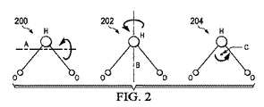
また図2〜図4を参照すると、図2は、それぞれ、3つの直交軸に沿った双極水分子の3つの回転モードを示す説明図200、202、及び204を提供し、図3は、電磁波周波数の関数として、種々のガスの回転モードに対する相対吸収のグラフ300を示す。図3に示されるように、水に対応する吸収ライン302が、この双極分子H2Oが低圧水蒸気に対して、識別可能な量子遷移周波数(183.31GHz)において、高い相対吸収を有し、また、同周波数範囲において、残りのガスよりはるかに高い吸収を有することを指す。
Referring also to FIGS. 2-4, FIG. 2 provides explanatory diagrams 200, 202, and 204, respectively, illustrating three rotation modes of a dipolar water molecule along three orthogonal axes. A
図4のグラフ400は、セルを通る伝送係数を、セルの内部の異なる圧力レベルに対する問い合わせ周波数の関数として示す。ここで、曲線402、404、406、408、410、及び412は、10mbarより大きい圧力(曲線402)、10mbarのキャビティ圧力(曲線404)、1.0mbar(曲線406)、0.1mbar(曲線408)、0.01mbar(曲線410)、及び0.01mbarより小さい圧力(曲線412)を含む、種々のキャビティ圧力に対応する。キャビティ103における双極水分子ガスに対する特定の実装が、クロックシステム100の動作において、ピーク吸収周波数での識別及びロックインを促進するために有利である。例えば、約0.1mbar又はそれ以下、及び約0.01mbar又はそれ以上等の、約1mbar又はそれ以下のキャビティ圧力が、水蒸気の場合において特定の動作利点を提供する。低圧処理チャンバにおいて密封されたキャビティ103を提供するために、図1における第1の基板102の頂部側に第2の基板106を取り付ける間、或る実装におけるキャビティ圧力は、接合プロセスの間、制御される。図4に示されるように、ピーク吸収(図4の吸収効率曲線において、ヌル又は相対的な最小)によって識別される量子遷移周波数は、キャビティ圧力の増大とともに増加する(例えば、一層幅が広くなる)。一層高いキャビティ圧力(例えば、室内圧力)での動作は、効率最小を識別することを困難にし得、従って、セルガスの量子周波数にロックインすることを困難にし得る。従って、特定の例は、図4における曲線406、408、及び410等の吸収におけるピークの品質係数を増加させるために、キャビティ103の内部の圧力を低減する。しかしながら、圧力における更なる低減は、キャビティ側壁104をヒットする分子に関連するドップラー及びその他のファクタの普及が増加することに起因して、収益漸減を引き起こし、また、双極分子の問い合わせの低減に起因して、圧力の低下とともに吸収ピークの規模は小さくなる。
The
図5〜図15は、コンパクトで低電力でコスト効率の良い解決策として、シリコン又は他の半導体ベースの集積回路プロセスを用いて蒸気セル101及び原子クロックシステム100が製造され得る、ウエハスケール又はチップスケール製造技術を示す。図5は、蒸気セル101を製造するためのプロセス又は方法500を、クロックシステム100を提供するために、製造された蒸気セル101を、その後、トランシーバ回路130と統合させるためにあり得る種々の相互接続技術と共に示す。図6〜図15は、方法500に従った製造処理の種々の段階におけるセル101を示す。例示のプロセス500は、ミリメートル波の導波路キャビティ103において低圧の双極分子ガスを有するコンパクトチップスケール蒸気セル101又は物理セルの直接パッケージングを促進し、それらは、ワイヤボンディング、フリップチップ、又は他のパッケージング技術を介してトランシーバダイと共にパッケージングされ得る。
5-15 illustrate a wafer scale or chip in which the
図5におけるプロセス500は、502で開始し、第1の基板102の第1の(例えば、頂部)側102aにおいてキャビティ103を形成する。1つの例において、第1の基板はシリコンウエハである。異なる例において、ガラス等の他の基板材料が用いられ得る。図6において示されるように、任意の適切なウェット又はドライエッチング処理602が図5における502でのキャビティ形成のために用いられ得る。幾つかの例において、複数の蒸気セル101を製造する等のために、単一の基板102に複数のキャビティ103が形成され得る。その際、図5における514において、個々の蒸気セル101を互いに分離させるために最終的なダイ分離が用いられる。キャビティ103の形は、図6に示されるようにハードマスク604を用いるパターニングによって、502において形成される。他の例において、高分子レジストが用いられ得る。高分子レジストは、KOH又はTMAHなどの強腐食性エッチャントを用いる等、プロセス602を介して、シリコン基板102のバルク異方性エッチングと共に、エッチャント(例えば、Brewer Science ProTekファミリーのレジスト)をレジストするように特別に製剤される。
The
エッチングプロセス602は、概して平滑な表面を有するキャビティ底部103bと共に、少なくとも1つの側壁104を形成する。その際、或る例におけるプロセス602は、蒸気セル101の動作において電磁的に誘導される電流損失を低減するために、約5μmRMS未満のキャビティ底部及び側壁粗さを提供する。別の例において、エッチングプロセス602は、シリコン基板102を通り、埋設されたエッチストップ層(図示せず)に至るまでエッチングする。埋設されたエッチストップ層は、シリコンを含む第1の基板を第2の基板(図示せず)に直接接合することによって形成され得る。第2の基板はシリコン又は別の材料(例えば、ガラス)で作成され、それらの間に誘電体層(例えば、二酸化ケイ素又は窒化ケイ素シリコン)を備える。そのような直接接合は、ウエハ接合のための幾つかの方法によって達成され得、1つの例は、最小コスト及び高スループットのために、低温プラズマ励起融着を用いる。図5の502におけるキャビティ形成、及び図6におけるエッチングプロセス602の後、必要であった全てのマスク604が除去され、クリーンアップ処理が実施され得る。
幾つかの例において、気相成長、スパッタリング、化学気相成長(CVD)、原子層堆積(ALD)等の任意の適切な堆積プロセスを用いてその後堆積される金属材料の接着を強化するために、キャビティ側壁104上及びキャビティ底部103b上に誘電体層が形成され得る。1つの適切な誘電体層は、銅に対する良好な接着性のため、五酸化タンタル(Ta2O5)である。
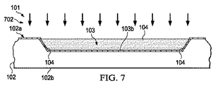
In some examples, to enhance the adhesion of subsequently deposited metal materials using any suitable deposition process such as vapor deposition, sputtering, chemical vapor deposition (CVD), atomic layer deposition (ALD), etc. A dielectric layer may be formed on the
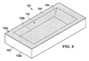
図5の504において、側壁104及びキャビティ底部103bの直上、又は任意の堆積された誘電体層の上に、図7に示されるように適切な堆積プロセス702を用いて、伝導性材料904が形成される。図8は、伝導性材料が、側壁104、キャビティ底部103b、及び第1の基板102の頂部側102a上に形成される、図7の伝導性材料堆積プロセス702の後の結果の第1の基板102を示す。1つの例において、堆積される伝導性材料は銅であり、キャビティ103の内部の電磁場によって誘導される電流に起因する損失を最小限にするように、表面粗さは約100nm又はそれ未満である。
In 504 of FIG. 5, a
1つの適切な堆積プロセス702は、高い伝導性、長距離磁気秩序がないこと、Ta2O5に対する良好な接着性、及び低コストを提供するための、堆積された誘電体層の上への銅金属のスパッタリングである。異なる例において、特性の同様の組み合わせを有するもの等、その他の金属材料が用いられ得る。1つの例においてスパッタ堆積に続いて、堆積コストを低減するために電気めっきを用いること等によって、銅又は所望され得るその他の金属を用いて、金属層が所望の均一の厚みに形成され得る。幾つかの例において、形成された金属層は、気相堆積又はその他の適切なプロセスを介して、誘電体材料で被覆され得る。或る例において、任意選択の誘電体材料が、予期される製品寿命の間、蒸気セル101の気相分子の金属層との反応を軽減するように選択され得る。下記に更に説明されるように、キャビティ103を閉鎖するため、第2の基板106との接合を促進するように、第1の基板102の頂部表面102aの全ての又は対象とする接合部分から、パターニング及びエッチングによって、含有される誘電体が全て除去され得る。この例において、図5の504において、側壁104及びキャビティ底部103b上に、完成した蒸気セル101の動作の周波数における表皮厚さより大きい厚みで伝導性材料が形成される。例えば、1つの例において、キャビティ103における信号損失を軽減するために、約50nm又はそれ以下の表面粗さを提供するように、約100nm又はそれ以上及び約1μm又はそれ以下等の厚みに形成される。
One
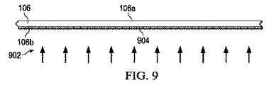
図5の506において、第2の基板106が、第1の又は頂部側106aと、第2の又は底部側106bとを有して提供される。図9に示されるような堆積プロセス902を用いて、第2の基板106の底部側106bに伝導性材料904が形成される。第2の基板106は、第1の基板102との接合を介してキャビティ頂部を形成するために後で用いられるものであり、蒸気セルの動作周波数の波長より小さい厚み(例えば、1つの例において、0.5mm未満)を有するガラス又はセラミックウエハ等の、任意の適切な材料であり得る。実際には、適切な第2の基板106は、キャビティ103への及びキャビティ103からの開口108を通してマイクロ波エネルギーの良好な電磁結合を促進するために充分薄く、真空下でキャビティ103を密封するために、第1の基板102に接合されるときの構造上の変形を軽減又は防止するために充分厚い。この点で、第2の基板の材料は、下記に説明されるように、材料904で形成され、後にパターニングされる非伝導性開口108を介して良好な電磁伝送率を提供することが好ましい。1つの適切な例は、0.2〜3.0mmの範囲の厚さのウエハ形態で入手可能な低アルカリのホウケイ酸ガラスである、Corning Eagle XG ガラスである。或る例において、後に誘電体の上に形成される金属膜の接着性を改善するために、第2の基板106は、各側106a及び106bで誘電体(例えば、Ta2O5)で被覆される。
In 506 of FIG. 5, a
図9〜図13に示されるように、伝導性材料の堆積及びパターニングは、第1の側106a及び第2の側106bに対して別々に行われ得る。1つの代替例において、頂部側106a及び底部側106bは、1つのステップで完全にメタライズされ得、その後、両方の側106a及び106bで所望の伝導性及び非伝導性領域を残すように選択的パターニングが行われる。図示された例において、底部側106bは、図5の508において、図10に示されるようにマスク1004を用いるエッチングプロセス1002を介してエッチングされて、底部側106bの伝導性材料904を通して、それぞれ、離間された第1の開口108a及び第2の開口108bが形成される。その際、底部側106bの残りは伝導性材料904で被覆されたままである。これらの開口又はスロット108は、図1に関連して上述したように、完成した蒸気セル101において電磁場がキャビティ103に入る又はキャビティ103から出ることを可能にする、電磁結合構造の一部を形成する。
As shown in FIGS. 9-13, the deposition and patterning of the conductive material can be performed separately for the
続いて、図5の510において、図11〜図14に示されるように、底部側106bに沿って形成される対応する開口108a及び108bの近くの、第2の基板106の第1の側106aに第1及び第2の伝導性結合構造110a及び110bが形成される。図11において、第1の側106aを銅又はその他の適切な伝導性材料1104でめっきするために堆積プロセス1102が用いられ、図13に示される第1及び第2の銅結合構造110a及び110bを形成するために、図12におけるエッチマスク1204と共に用いてエッチングプロセス1202が用いられる。更に図14に示されるように、1つの例において、伝導性結合構造110a及び110bは、導波路キャビティ103の内部と電磁的結合するために、それぞれ、下にある開口108a及び108bを長手方向に横切って延びる伝導性ストリップとして形成される。後続の、ホストトランシーバ130(例えば、図1)とのパッケージングにおいて、結合構造110は、ホスト集積回路パッケージ又は印刷回路基板(図示せず)に取り付けられる完成した蒸気セル構造101との、シンプルでコスト効率のよいパッケージングアッセンブリを提供するように、任意の適切なフリップチップ、ワイヤボンディング、又はその他の電気的相互接続技術を用いて、入力133及び138に電気的に結合され得る。動作において、第1の結合構造110aは、トランシーバ130の出力133から送信信号TXを受け取り、磁場を生成し、その磁場は開口108aを通して、密封されたキャビティ103の内部の双極分子ガスに向けられる。
Subsequently, at 510 in FIG. 5, as shown in FIGS. 11-14, the
図12〜図14に更に示されるように、この例はまた、図12におけるエッチマスク1204を介して蒸気セル101の外側表面106a上に形成されるパターニングされた伝導性電子バンドギャップ(EBG)構造120(図13、及び図14)を含む。EBG構造120は、スプリアスの表面波の伝搬を防止又は軽減するため、伝導性結合構造110から離間される。図14の例において、第1及び第2のEBG構造120a及び120bは、各々3列の、伝導性材料1104の幾つかの繰り返しパターンを含み、周波数の所与の目標バンドギャップ範囲の第2の基板106の第1の側106aに沿って電磁波結合を減衰させるために任意の適切なパターンが用いられ得る。その際、EBG構造120は、送信結合構造110a及び受信結合110bから離間され、それらの間に配置される。他の例において、単一のEBG構造120のみが、結合構造110a及び110bから離間され、それらの間に配置されて用いられる。その他のあり得る例は、第1の側106aに沿って電磁波結合を減衰させるために、2つより多くのEBG構造120を含む。他の例において、EBG構造120は省かれる。
As further shown in FIGS. 12-14, this example also illustrates a patterned conductive electron bandgap (EBG) structure formed on the
図14の例示の第2の基板106において示されるように、開口108及び結合構造110は、両方とも延伸された長方形であるが、他の例では、その他の形状及び相対位置が用いられ得る。種々の例において、開口108は、キャビティ103内のTE01モードの伝搬の方向に垂直又は平行のいずれかであり得る。トランシーバ回路130が高い周波数TX信号(例えば、種々の例において、100〜1000GHz)を蒸気セル101に提供するので、また、或る例において、第2の基板106が波長のフラクションの厚みを有するので、表面波は、接地された誘電体スラブに沿って、又はセル101の頂部表面106aに沿って伝搬し得、導波路の入力及び出力開口108間で結合し得、それによって、蒸気セルのキャビティ103を通過しない信号のための第2の経路が生成され、そのような余分のキャビティ送信は、動作において、キャビティ103内の双極分子ガスの吸収をマスキングし得る。
As shown in the exemplary
従って、幾つかの例は、光バンドギャップ構造としての動作を介してそのような表面波を軽減するように、1つ又は複数のEBG構造120を含む。1つの例において、EBG構造120は、表面波の伝搬を軽減又は防止するために、周波数の予期される動作範囲にバンドギャップを有し、それによって蒸気セル101に問い合わせるために用いられる周波数の範囲に調整されている。EBGは、第2の基板106の第2の又は底部側106bの伝導性層904と、第1の又は頂部側106aの反復する単位セル120のパターニングされたアレイとの平行組み合わせを含む、調整されたフィルタである。図示された例においてビアは必要ではないが、他の例においてビアが用いられ得る。1つの例において、導波路キャビティ103は、伝搬定数、及び最初の3つのモードに対するカットオフを提供するために、1.5mmの頂部幅及び0.5mmのエッチ深さでエッチングされる。3つのモードは、第1のモードが120GHzで開始し、第2のモードが230GHzで開始し、及び第3のモードが290GHzで開始する。キャビティ103は、1つの例において、第1のモードのみが伝搬し得る(これは、他の例において、導波路寸法を変えることによって調整され得る)周波数範囲における動作に対して設計される。この例において、160〜195GHzの範囲の周波数のバンドギャップが存在する。その範囲では、どのモードも頂部側106aに沿って伝搬することはなく、その際、EBGアレイ120は、対象のバンドギャップにおいて、電磁信号に対する第2の経路を防止するように導波路の2つのポートの間に配置される。
Thus, some examples include one or more EBG structures 120 to mitigate such surface waves through operation as an optical bandgap structure. In one example, the EBG structure 120 has a band gap in the expected operating range of frequencies to reduce or prevent surface wave propagation, and thereby the range of frequencies used to interrogate the
続いて、図5の512において、低圧の双極分子ガスH20を含む密封されたキャビティ103を形成するために、第2の基板106の底部側106bは、図15の接合プロセス1500を介して、低い周囲圧力において双極分子ガス(例えば、H2O)を含む周囲環境において、第1の基板102の第1の側102に接合される。接合プロセス1500は、キャビティ103内部にいかなる不要なガスも導入せず、低圧の双極分子蒸気でキャビティ103を密封する、任意の適切なウエハ接合ステップであり得る。適切な金属接合プロセス例1500には、或る低い温度で形成され、それらが形成される温度よりはるかに高い再溶融温度を有するような、固液相互拡散(SLID)接合又は過渡液相(TLP)接合を形成することが含まれる。共通TLP接合される金属結合には、Au/In、Cu/Sn、Sn/Au、Sn/Agが含まれ、金属結合は、利便性及び最終デバイスジオメトリとの全体的な互換性に対して選択され得る。或る例において、キャビティ圧力はマイクロトールからミリトールの範囲であり、従って、512において、基板102及び106は、熱及び蒸気の両方を提供及び制御することが可能な処理チャンバにおいて接合及び密封される。接合プロセス1500のための適切な処理チャンバは、オーストリアのElectronic Visions Group(EVG)等の供給元から市販されている。基板102及び106は、チャンバ内に置かれ、水、アセトニトリル、又はフッ化メチル等の所望の双極分子蒸気の小分圧を備える適切な真空ヘッドスペースが構築される。基板102及び106は、その後、処理されたウエハの各々別個のキャビティ103の不浸透性シールをつくるために対応する適切な温度プロファイルに従って接合される。その際、全てのキャビティが、ウエハレベルにおいて基本的に同時に接合される。代替の実装において、キャビティ103は、揮発性の種の悪化及び損失を軽減するため、周囲のダイの一層低い温度を維持しつつ、接合領域を適切な温度まで局所的に加熱するためにレーザ放射を用いる装置によって、順次密封され得る。
Subsequently, at 512 of FIG. 5, the
図5の514において、所望の濃度の低圧双極分子ガスを含むデバイスは、適切な半導体ダイシング技術を用いてシンギュレートされる。完成した蒸気セル101(物理セル)は、その後、ピックアンドプレイス、又は完全に統合されたシステムソリューションのためにワイヤボンディングを介する他のマイクロ波デバイスとの接続すること等の、更なる処理に利用可能である。 In 514 of FIG. 5, the device containing the desired concentration of low pressure bipolar molecular gas is singulated using a suitable semiconductor dicing technique. The completed vapor cell 101 (physical cell) is then used for further processing, such as pick-and-place or connecting to other microwave devices via wire bonding for a fully integrated system solution Is possible.
図16は、関連するトランシーバ回路130(例えば、図1)を介する問い合わせの間の動作における、完成した単一蒸気セル装置101のシンプルな平面図である。電磁場1600を入力開口108aを介してキャビティ103の内部に結合するために、交流電気出力信号TXがトランシーバ出力133を介して第1の伝導性結合構造110aに提供される。電磁場1600は、交流電気入力信号RXを、第2の結合構造110bを介してトランシーバ入力138に提供するために、キャビティ103の長手方向長さLに沿って出口開口108bまで延びる。上述したように、完成した蒸気セル101は、電磁波を減衰するために、セル構造101の頂部側に沿って置かれる1つ又は複数のEBG構造120(例えば、図1)を含み得る。EBG構造120は、キャビティ103の内部の電磁場1600の説明を容易にするために、図16から省かれている。
FIG. 16 is a simple top view of the completed single
図17は、上記で詳細に説明した原理を用いて構成される別の蒸気セル例101を示し、コンパクトデバイス101を提供するために、セルキャビティは、長さ及び従って吸収を増加させるように非線形経路に沿って蛇行している。セル構造101の全体の長さは短くなるが、図17における吸収長Lは、図16のセル101の吸収長Lより長い。線形又は非線形の経路に沿って延びるセルキャビティ103を含む他の例(線形及び非線形部分の組み合わせ、曲線部分、段階的線形部分、及びそれらの組み合わせを含む)が可能であり、例示の実施形態は図示された例に限定されない。
FIG. 17 illustrates another
図18は、別の蒸気セル例101を図示し、キャビティ103が第3の伝導性開口108c及び第4の伝導性開口108dを含み、各々の伝導性結合構造110は、対の非伝導性開口に近い。この例において、開口108a及び108cは互いに平行であり、対応する送信結合構造110aは、平行な対の開口108a及び108cを横切って、概ね垂直に延びる。同様に、非伝導性の底部側開口108b及び108dは互いに対して概ね平行である。その際、関連する受信伝導性結合構造110bは、対応するレシーバ開口108b及び108dに垂直に、及び対応するレシーバ開口108b及び108dの上に延在する。この例において、第3の開口108cは、キャビティ103への第2の電磁場入口を提供し、第4の非伝導性開口108dは、キャビティ103からの別の電磁場出口を提供する。他の例において、キャビティ103の内部との電磁結合のために、1つ又は複数の伝導性結合構造110と1つ又は複数の開口108との他の組み合わせが用いられ得る。
FIG. 18 illustrates another
従って、例示の実施形態は、基準を設定するために電子遷移を用いる従来の原子クロックの複雑性、電力消費、サイズの欠点を回避しつつ、基準クロック信号REFCLKを提供するために低圧ガス分子の回転量子遷移を用いる、シンプルでコスト効率のよい低電力動作で、ミリメートル波原子クロック100、及びそのための回転遷移蒸気セル101を提供する。開示される回転遷移ベースの原子クロックの概念は、温度変動に安定であり、チップスケール又はウエハスケール処理技術を用いて製造され得る。更に、開示されるクロック100は、低圧双極分子蒸気の回転量子状態を確実にし、それにロックインするように、電子遷移デバイスよりはるかに低い周波数で動作し、また開示される技術は、従来の光学的問い合わせ蒸気セルにおけるような、クリアな光学送信経路の提供に関連する問題を回避する。更に、開示される蒸気セル101は、種々の低コストなミリメートル波CMOSトランシーバ回路130を用いて、遷移を網羅する帯域幅にわたって物理セル101内の低圧双極分子ガスを問い合わせるのに有用である。更に、水及びその他の双極分子ガスは、遷移周波数で、検出可能な吸収変化を示し、安定した基準クロック信号を提供するためのロックインを促進する。蒸気セル101及び全体の原子クロックシステム100は、或る例において、シリコン製造及びパッケージングプロセス内で構成及びパッケージングされ得る。更に、開示されるチップスケールの双極分子蒸気セル101は、原子クロック、及び回転分光学に関連する他の用途において有用であり、他の回転分光学ソリューションよりコンパクトな設計を提供する。
Thus, the exemplary embodiment avoids the drawbacks of the complexity, power consumption, and size of conventional atomic clocks that use electronic transitions to set the reference, while providing low-pressure gas molecules to provide the reference clock signal REFCLK. A millimeter wave
本発明の請求の範囲内で、説明された実施形態において変更が可能であり、また、他の実施形態が可能である。 Within the scope of the claims, changes may be made in the described embodiments, and other embodiments are possible.
Claims (20)
蒸気セル、及びトランシーバ回路を含み、
前記蒸気セルが、キャビティ、双極分子ガス、第1の伝導性結合構造、及び第2の伝導性結合構造を含み、
前記キャビティが、伝導性内部キャビティ表面を備える密封された内部と、前記キャビティに電磁場入口を提供するための、前記内部キャビティ表面における第1の非伝導性開口と、前記キャビティからの電磁場出口を提供するための、前記内部キャビティ表面における前記第1の非伝導性開口から離間された第2の非伝導性開口とを含み、
前記双極分子ガスが前記キャビティの前記密封された内部の内側にあり、
第1の伝導性結合構造が前記第1の非伝導性開口の近くの前記蒸気セルの外側表面上に形成され、
第2の伝導性結合構造が、前記第2の非伝導性開口の近くの前記蒸気セルの前記外側表面上に形成され、
前記トランシーバ回路が、
交流電気出力信号を、電磁場を前記キャビティの前記内部に結合するための前記第1の伝導性結合構造に提供するためのものであり、
前記キャビティから受け取る前記電磁場を表す、前記第2の伝導性結合構造からの交流電気入力信号を受け取るためのものであり、
前記電気入力信号を低減するように、前記電気出力信号の周波数を選択的に調整するためのものであり、及び
前記電気出力信号の前記周波数において基準クロック信号を提供するためのものである、
クロック装置。 A clock device,
Including a steam cell and a transceiver circuit;
The vapor cell includes a cavity, a bipolar molecular gas, a first conductive coupling structure, and a second conductive coupling structure;
The cavity provides a sealed interior with a conductive internal cavity surface, a first non-conductive opening in the internal cavity surface for providing an electromagnetic field entrance to the cavity, and an electromagnetic field exit from the cavity A second non-conductive opening spaced from the first non-conductive opening in the inner cavity surface to
The bipolar molecular gas is inside the sealed interior of the cavity;
A first conductive coupling structure is formed on the outer surface of the vapor cell near the first non-conductive opening;
A second conductive coupling structure is formed on the outer surface of the vapor cell near the second non-conductive opening;
The transceiver circuit comprises:
Providing an alternating electrical output signal to the first conductive coupling structure for coupling an electromagnetic field to the interior of the cavity;
For receiving an alternating electrical input signal from the second conductive coupling structure representing the electromagnetic field received from the cavity;
For selectively adjusting the frequency of the electrical output signal so as to reduce the electrical input signal, and for providing a reference clock signal at the frequency of the electrical output signal;
Clock device.
前記キャビティが、
前記キャビティへの別の電磁場入口を提供するための、前記内部キャビティ表面における前記第1の非伝導性開口から離間された第3の非伝導性開口、及び
前記キャビティからの別の電磁場出口を提供するための、前記内部キャビティ表面における前記第2の非伝導性開口から離間された第4の非伝導性開口、
を含み、
前記第1の伝導性結合構造が前記第1及び第3の非伝導性開口に近く、前記第2の伝導性結合構造が前記第2及び第4の非伝導性開口に近い、
クロック装置。 The clock device according to claim 1,
The cavity is
Providing a third non-conductive opening spaced from the first non-conductive opening in the inner cavity surface to provide another electromagnetic field entrance to the cavity; and another electromagnetic field outlet from the cavity A fourth non-conductive opening spaced from the second non-conductive opening in the inner cavity surface to
Including
The first conductive coupling structure is close to the first and third non-conductive openings, and the second conductive coupling structure is close to the second and fourth non-conductive openings;
Clock device.
前記トランシーバ回路が、
前記交流電気出力信号を前記第1の伝導性結合構造に提供するために、及び前記電気出力信号の周波数で前記基準クロック信号を提供するために、前記第1の伝導性結合構造と電気的に結合される出力を備える信号生成器、
前記交流電気入力信号を受け取るために、及び前記電気入力信号と前記電気出力信号との間の差を表す誤差信号を提供するために、前記第2の伝導性結合構造と電気的に結合される入力を備えるロックイン増幅器、及び
前記誤差信号を受け取るための、及び前記電気出力信号の周波数を前記キャビティの前記密封された内部の内側の前記双極分子ガスのピーク吸収周波数で維持するように前記電気出力信号の周波数を選択的に調整するために、制御出力信号を前記信号生成器に提供するためのループフィルタ、
を含む、
クロック装置。 The clock device according to claim 1,
The transceiver circuit comprises:
In order to provide the alternating electrical output signal to the first conductive coupling structure and to provide the reference clock signal at a frequency of the electrical output signal, electrically with the first conductive coupling structure A signal generator with a combined output,
Electrically coupled to the second conductive coupling structure to receive the alternating electrical input signal and to provide an error signal representative of a difference between the electrical input signal and the electrical output signal A lock-in amplifier with an input; and for receiving the error signal and for maintaining the frequency of the electrical output signal at the peak absorption frequency of the bipolar molecular gas inside the sealed interior of the cavity. A loop filter for providing a control output signal to the signal generator to selectively adjust the frequency of the output signal;
including,
Clock device.
前記蒸気セルが、第1の基板及び第2の基板を含み、
前記第1の基板が、第1の側、前記第1の側の内方に向けて延びる少なくとも1つのキャビティ側壁、及びキャビティ底部を含み、
前記第2の基板が、第1の側、及びキャビティ頂部を含む第2の側を含み、前記少なくとも1つのキャビティ側壁、前記キャビティ底部、及び前記第2の基板の前記第2の側に少なくとも部分的に沿って延びる前記伝導性内部キャビティ表面を備える前記密封された内部を含む前記キャビティを形成するように、前記第2の基板の前記第2の側が、前記第1の基板の前記第1の側に取り付けられ、
前記第1及び第2の非伝導性開口が、それぞれ、前記電磁場入口及び出口を提供するために、前記第2の基板の前記第2の側上の前記内部キャビティ表面に形成され、
前記第1及び第2の伝導性結合構造が前記第2の基板の前記第1の側に形成される、
クロック装置。 The clock device according to claim 1,
The vapor cell includes a first substrate and a second substrate;
The first substrate includes a first side, at least one cavity sidewall extending inwardly of the first side, and a cavity bottom;
The second substrate includes a first side and a second side including a cavity top, at least partially on the at least one cavity sidewall, the cavity bottom, and the second side of the second substrate. The second side of the second substrate is the first side of the first substrate so as to form the cavity including the sealed interior with the conductive inner cavity surface extending along. Attached to the side,
Said first and second non-conductive openings are formed in said internal cavity surface on said second side of said second substrate to provide said electromagnetic field inlet and outlet, respectively;
The first and second conductive coupling structures are formed on the first side of the second substrate;
Clock device.
前記双極分子ガスが、前記キャビティの前記密封された内部の内側で、約0.1mbar又はそれ以下の圧力であり、
前記双極分子ガスが、前記キャビティの前記密封された内部の内側で、約0.01mbar又はそれ以上の圧力である、
クロック装置。 The clock device according to claim 8, wherein
The bipolar molecular gas is at a pressure of about 0.1 mbar or less inside the sealed interior of the cavity;
The bipolar molecular gas is at a pressure of about 0.01 mbar or more inside the sealed interior of the cavity;
Clock device.
キャビティ、双極分子ガス、第1の伝導性結合構造、及び第2の伝導性結合構造を含み、
前記キャビティが、少なくとも1つの基板において形成され、前記キャビティが、伝導性内部キャビティ表面を備える密封された内部と、前記キャビティに電磁場入口を提供するための、前記内部キャビティ表面における第1の非伝導性開口と、前記キャビティに電磁場出口を提供するための、前記内部キャビティ表面における前記第1の非伝導性開口から離間された第2の非伝導性開口とを含み、
前記双極分子ガスが、前記キャビティの前記密封された内部の内側にあり、
前記第1の伝導性結合構造が、前記第1の非伝導性開口に近い前記蒸気セルの外側表面上に形成され、
前記第2の伝導性結合構造が、前記第2の非伝導性開口に近い前記蒸気セルの前記外側表面上に形成される、
蒸気セル。 A steam cell,
Including a cavity, a bipolar molecular gas, a first conductive coupling structure, and a second conductive coupling structure;
The cavity is formed in at least one substrate, the cavity being a sealed interior with a conductive interior cavity surface and a first non-conductivity at the interior cavity surface to provide an electromagnetic field entrance to the cavity. And a second non-conductive opening spaced from the first non-conductive opening at the inner cavity surface for providing an electromagnetic field exit to the cavity;
The bipolar molecular gas is inside the sealed interior of the cavity;
The first conductive coupling structure is formed on an outer surface of the vapor cell near the first non-conductive opening;
The second conductive coupling structure is formed on the outer surface of the vapor cell proximate to the second non-conductive opening;
Steam cell.
前記キャビティが、
前記キャビティへの別の電磁場入口を提供するための、前記内部キャビティ表面における前記第1の非伝導性開口から離間された第3の非伝導性開口、及び
前記キャビティからの別の電磁場出口を提供するための、前記内部キャビティ表面における前記第2の非伝導性開口から離間された第4の非伝導性開口、
を含み、
前記第1の伝導性結合構造が前記第1及び第3の非伝導性開口に近く、前記第2の伝導性結合構造が前記第2及び第4の非伝導性開口に近い、
蒸気セル。 The steam cell according to claim 11,
The cavity is
Providing a third non-conductive opening spaced from the first non-conductive opening in the inner cavity surface to provide another electromagnetic field entrance to the cavity; and another electromagnetic field outlet from the cavity A fourth non-conductive opening spaced from the second non-conductive opening in the inner cavity surface to
Including
The first conductive coupling structure is close to the first and third non-conductive openings, and the second conductive coupling structure is close to the second and fourth non-conductive openings;
Steam cell.
第1の基板及び第2の基板を含み、
前記第1の基板が、第1の側と、前記第1の側の内方に向けて延びる少なくとも1つのキャビティ側壁と、キャビティ底部とを含み、
前記第2の基板が、第1の側と、キャビティ頂部を含む第2の側とを含み、前記少なくとも1つのキャビティ側壁、前記キャビティ底部、及び前記第2の基板の前記第2の側に少なくとも部分的に沿って延びる前記伝導性内部キャビティ表面を備える前記密封された内部を含む前記キャビティを形成するように、前記第2の基板の前記第2の側が、前記第1の基板の前記第1の側に取り付けられ、
前記第1及び第2の非伝導性開口が、それぞれ、前記電磁場入口及び出口を提供するために、前記第2の基板の前記第2の側の前記内部キャビティ表面に形成され、
前記第1及び第2の伝導性結合構造が前記第2の基板の前記第1の側に形成される、
蒸気セル。 The steam cell according to claim 11,
Including a first substrate and a second substrate;
The first substrate includes a first side, at least one cavity sidewall extending inwardly of the first side, and a cavity bottom;
The second substrate includes a first side and a second side including a cavity top, at least on the at least one cavity sidewall, the cavity bottom, and the second side of the second substrate. The second side of the second substrate is the first side of the first substrate so as to form the cavity including the sealed interior with the conductive inner cavity surface extending partially along the surface. Attached to the side of
Said first and second non-conductive apertures are formed in said internal cavity surface on said second side of said second substrate to provide said electromagnetic field inlet and outlet, respectively;
The first and second conductive coupling structures are formed on the first side of the second substrate;
Steam cell.
前記双極分子ガスが、前記キャビティの前記密封された内部の内側で、約0.1mbar又はそれ以下の圧力であり、
前記双極分子ガスが、前記キャビティの前記密封された内部の内側で、約0.01mbar又はそれ以上の圧力である、
蒸気セル。 A steam cell according to claim 17,
The bipolar molecular gas is at a pressure of about 0.1 mbar or less inside the sealed interior of the cavity;
The bipolar molecular gas is at a pressure of about 0.01 mbar or more inside the sealed interior of the cavity;
Steam cell.
第1の基板の第1の側の中にキャビティを形成すること、
前記キャビティの少なくとも1つの側壁及び底部に伝導性材料を形成すること、
第2の基板の底部側に伝導性材料を形成すること、
前記第2の基板の前記底部側の前記伝導性材料を通して、第1及び第2の離間された開口をエッチングすること、
前記第2の基板の頂部側に第1及び第2の伝導性結合構造を形成すること、及び
双極分子ガスを含む周囲環境において、前記双極分子ガスを含む密封されたキャビティを形成するように、前記第2の基板の前記底部側を前記第1の基板の前記第1の側に接合すること、
を含む、方法。 A method of manufacturing a steam cell, comprising:
Forming a cavity in the first side of the first substrate;
Forming a conductive material on at least one sidewall and bottom of the cavity;
Forming a conductive material on the bottom side of the second substrate;
Etching first and second spaced openings through the conductive material on the bottom side of the second substrate;
Forming first and second conductive coupling structures on the top side of the second substrate, and forming a sealed cavity containing the bipolar molecular gas in an ambient environment containing the bipolar molecular gas; Bonding the bottom side of the second substrate to the first side of the first substrate;
Including a method.
Applications Claiming Priority (3)
| Application Number | Priority Date | Filing Date | Title |
|---|---|---|---|
| US14/674,197 US9529334B2 (en) | 2015-03-31 | 2015-03-31 | Rotational transition based clock, rotational spectroscopy cell, and method of making same |
| US14/674,197 | 2015-03-31 | ||
| PCT/US2016/025445 WO2016161215A1 (en) | 2015-03-31 | 2016-03-31 | Rotational transition based clock, rotational spectroscopy cell, and method of making same |
Publications (2)
| Publication Number | Publication Date |
|---|---|
| JP2018515012A true JP2018515012A (en) | 2018-06-07 |
| JP2018515012A5 JP2018515012A5 (en) | 2019-05-09 |
Family
ID=57005350
Family Applications (1)
| Application Number | Title | Priority Date | Filing Date |
|---|---|---|---|
| JP2017551694A Pending JP2018515012A (en) | 2015-03-31 | 2016-03-31 | Rotating transition based clock, rotating spectroscopic cell, and method of creating them |
Country Status (5)
| Country | Link |
|---|---|
| US (1) | US9529334B2 (en) |
| EP (1) | EP3278184B1 (en) |
| JP (1) | JP2018515012A (en) |
| CN (1) | CN107209480B (en) |
| WO (1) | WO2016161215A1 (en) |
Cited By (2)
| Publication number | Priority date | Publication date | Assignee | Title |
|---|---|---|---|---|
| JP2021524999A (en) * | 2018-05-10 | 2021-09-16 | テキサス インスツルメンツ インコーポレイテッド | Compact millimeter wave system |
| JP2022551759A (en) * | 2019-11-27 | 2022-12-13 | クオンタム ヴァリー アイデアズ ラボラトリーズ | Photonic crystal vapor cell for electromagnetic imaging |
Families Citing this family (27)
| Publication number | Priority date | Publication date | Assignee | Title |
|---|---|---|---|---|
| US10498001B2 (en) | 2017-08-21 | 2019-12-03 | Texas Instruments Incorporated | Launch structures for a hermetically sealed cavity |
| US10775422B2 (en) | 2017-09-05 | 2020-09-15 | Texas Instruments Incorporated | Molecular spectroscopy cell with resonant cavity |
| US10589986B2 (en) * | 2017-09-06 | 2020-03-17 | Texas Instruments Incorporated | Packaging a sealed cavity in an electronic device |
| US10131115B1 (en) | 2017-09-07 | 2018-11-20 | Texas Instruments Incorporated | Hermetically sealed molecular spectroscopy cell with dual wafer bonding |
| US10444102B2 (en) * | 2017-09-07 | 2019-10-15 | Texas Instruments Incorporated | Pressure measurement based on electromagnetic signal output of a cavity |
| US10549986B2 (en) * | 2017-09-07 | 2020-02-04 | Texas Instruments Incorporated | Hermetically sealed molecular spectroscopy cell |
| US10424523B2 (en) | 2017-09-07 | 2019-09-24 | Texas Instruments Incorporated | Hermetically sealed molecular spectroscopy cell with buried ground plane |
| US10551265B2 (en) * | 2017-09-07 | 2020-02-04 | Texas Instruments Incorporated | Pressure sensing using quantum molecular rotational state transitions |
| US10544039B2 (en) * | 2017-09-08 | 2020-01-28 | Texas Instruments Incorporated | Methods for depositing a measured amount of a species in a sealed cavity |
| US10364144B2 (en) | 2017-11-17 | 2019-07-30 | Texas Instruments Incorporated | Hermetically sealed package for mm-wave molecular spectroscopy cell |
| US10370760B2 (en) * | 2017-12-15 | 2019-08-06 | Texas Instruments Incorporated | Methods for gas generation in a sealed gas cell cavity |
| US10754302B2 (en) | 2017-12-29 | 2020-08-25 | Texas Instruments Incorporated | Molecular atomic clock with wave propagating rotational spectroscopy cell |
| US10649408B2 (en) * | 2017-12-29 | 2020-05-12 | Texas Instruments Incorporated | Molecular atomic clock with wave propagating rotational spectroscopy cell |
| US10859980B2 (en) * | 2017-12-29 | 2020-12-08 | Texas Instruments Incorporated | Molecular atomic clock with wave propagating rotational spectroscopy cell |
| US10739728B2 (en) * | 2018-01-29 | 2020-08-11 | Massachusetts Institute Of Technology | Molecular clock |
| US10823668B2 (en) * | 2018-04-24 | 2020-11-03 | Honeywell International Inc. | Apparatuses and methods for alkali spectroscopy |
| JP6866884B2 (en) * | 2018-10-04 | 2021-04-28 | カシオ計算機株式会社 | Cases, watches, how to make cases and how to make watches |
| US11105681B2 (en) * | 2018-11-28 | 2021-08-31 | Texas Instruments Incorporated | Spectroscopy cavity with digital activation of millimeter wave molecular headspace |
| US11188032B2 (en) * | 2019-02-08 | 2021-11-30 | Texas Instruments Incorporated | Molecular clock with delay compensation |
| US11204513B2 (en) * | 2019-05-03 | 2021-12-21 | Yissum Research Development Company Of The Hebrew University Of Jerusamem Ltd | Integrated frequency referencing system |
| US11204378B2 (en) * | 2019-12-30 | 2021-12-21 | Texas Instruments Incorporated | Background suppression for MM-wave spectroscopy |
| US11782392B2 (en) | 2020-10-06 | 2023-10-10 | Texas Instruments Incorporated | Hermetic vial for quantum transitions detection in electronic devices applications |
| US11467228B2 (en) | 2020-11-11 | 2022-10-11 | Texas Instruments Incorporated | Millimeter wave magnetic sensor |
| US11677406B2 (en) * | 2020-12-31 | 2023-06-13 | Texas Instruments Incorporated | Package for millimeter wave molecular clock |
| US11600581B2 (en) | 2021-04-15 | 2023-03-07 | Texas Instruments Incorporated | Packaged electronic device and multilevel lead frame coupler |
| FI20215481A1 (en) | 2021-04-26 | 2022-10-27 | Teknologian Tutkimuskeskus Vtt Oy | High-frequency electronic module |
| US20240048145A1 (en) * | 2022-08-08 | 2024-02-08 | Northrop Grumman Systems Corporation | Atomic clock system |
Family Cites Families (22)
| Publication number | Priority date | Publication date | Assignee | Title |
|---|---|---|---|---|
| US2699503A (en) * | 1949-04-30 | 1955-01-11 | Lyons Harold | Atomic clock |
| FR1468760A (en) | 1965-08-04 | 1967-02-10 | Csf | Atomic clocks with spin exchange collisions |
| US6172570B1 (en) * | 1999-08-23 | 2001-01-09 | Datum, Inc. | Laser light quantum system |
| JP3811079B2 (en) * | 2002-02-05 | 2006-08-16 | 富士通株式会社 | Atomic oscillator |
| US20060022761A1 (en) | 2004-07-16 | 2006-02-02 | Abeles Joseph H | Chip-scale atomic clock (CSAC) and method for making same |
| US7468637B2 (en) * | 2006-04-19 | 2008-12-23 | Sarnoff Corporation | Batch-fabricated, RF-interrogated, end transition, chip-scale atomic clock |
| GB0712696D0 (en) | 2007-06-29 | 2007-08-08 | Isis Innovation | Atomic clock |
| DE102007034963B4 (en) * | 2007-07-26 | 2011-09-22 | Universität des Saarlandes | A cell having a cavity and a wall surrounding the cavity, a process for producing such a cell, the use thereof, and a wall with a recess which can be formed therein |
| GB2454203A (en) * | 2007-10-30 | 2009-05-06 | Univ Muenster Wilhelms | Time controlled activation of elements |
| US7825736B2 (en) | 2008-12-18 | 2010-11-02 | Princeton University | Method for suppressing light shift in optical pumping systems |
| US8906470B2 (en) | 2011-05-26 | 2014-12-09 | CSEM Centre Suisse d'Electronique et de Microtechnique SA—Recherche et Developpment | Method for producing a microfabricated atomic vapor cell |
| US8624682B2 (en) | 2011-06-13 | 2014-01-07 | Honeywell International Inc. | Vapor cell atomic clock physics package |
| US9201124B2 (en) | 2011-07-14 | 2015-12-01 | National Semiconductor Corporation | Die-sized atomic magnetometer and method of forming the magnetometer |
| US8836327B2 (en) | 2011-12-07 | 2014-09-16 | Texas Instruments Incorporated | Micro-fabricated atomic magnetometer and method of forming the magnetometer |
| US9024397B2 (en) | 2012-01-07 | 2015-05-05 | Texas Instruments Incorporated | Thermally-insulated micro-fabricated atomic clock structure and method of forming the atomic clock structure |
| CN102799101B (en) * | 2012-02-15 | 2013-09-18 | 中国科学院武汉物理与数学研究所 | Physical system device for chip coherent population trapping (CPT) atomic clock |
| US9429528B2 (en) | 2013-05-23 | 2016-08-30 | Texas Instruments Incorporated | Determining gas absorption line from separate and alternating RF signals |
| US9325334B2 (en) | 2013-06-12 | 2016-04-26 | Texas Instruments Incorporated | IC, process, device generating frequency reference from RF gas absorption |
| US20140373599A1 (en) | 2013-06-25 | 2014-12-25 | Texas Instruments Incorporated | Detection and locking to the absorption spectra of gasses using quartz enhanced photoacoustic sprectroscopy |
| US20150001694A1 (en) | 2013-07-01 | 2015-01-01 | Texas Instruments Incorporated | Integrated circuit device package with thermal isolation |
| US9568565B2 (en) | 2013-07-23 | 2017-02-14 | Texas Instruments Incorporated | Vapor cell structure having cavities connected by channels for micro-fabricated atomic clocks, magnetometers, and other devices |
| US9169974B2 (en) | 2013-07-23 | 2015-10-27 | Texas Instruments Incorporated | Multiple-cavity vapor cell structure for micro-fabricated atomic clocks, magnetometers, and other devices |
-
2015
- 2015-03-31 US US14/674,197 patent/US9529334B2/en active Active
-
2016
- 2016-03-31 JP JP2017551694A patent/JP2018515012A/en active Pending
- 2016-03-31 CN CN201680009669.4A patent/CN107209480B/en active Active
- 2016-03-31 EP EP16774275.8A patent/EP3278184B1/en active Active
- 2016-03-31 WO PCT/US2016/025445 patent/WO2016161215A1/en active Application Filing
Cited By (3)
| Publication number | Priority date | Publication date | Assignee | Title |
|---|---|---|---|---|
| JP2021524999A (en) * | 2018-05-10 | 2021-09-16 | テキサス インスツルメンツ インコーポレイテッド | Compact millimeter wave system |
| JP7277008B2 (en) | 2018-05-10 | 2023-05-18 | テキサス インスツルメンツ インコーポレイテッド | Compact millimeter wave system |
| JP2022551759A (en) * | 2019-11-27 | 2022-12-13 | クオンタム ヴァリー アイデアズ ラボラトリーズ | Photonic crystal vapor cell for electromagnetic imaging |
Also Published As
| Publication number | Publication date |
|---|---|
| EP3278184A1 (en) | 2018-02-07 |
| CN107209480B (en) | 2020-06-16 |
| EP3278184B1 (en) | 2020-04-22 |
| EP3278184A4 (en) | 2018-04-25 |
| CN107209480A (en) | 2017-09-26 |
| US9529334B2 (en) | 2016-12-27 |
| US20160291549A1 (en) | 2016-10-06 |
| WO2016161215A1 (en) | 2016-10-06 |
Similar Documents
| Publication | Publication Date | Title |
|---|---|---|
| EP3278184B1 (en) | Rotational transition based clock, rotational spectroscopy cell, and method of making same | |
| CN109799695B (en) | Hermetically sealed package for millimeter wave molecular spectroscopy cells | |
| US10370760B2 (en) | Methods for gas generation in a sealed gas cell cavity | |
| US20200106152A1 (en) | Launch structures for a hermetically sealed cavity | |
| US10510513B2 (en) | Plasma processing device and high-frequency generator | |
| US10493722B2 (en) | Hermetically sealed molecular spectroscopy cell with dual wafer bonding | |
| US20240045381A1 (en) | Molecular Atomic Clock With Wave Propagating Rotational Spectroscopy Cell | |
| US10976708B2 (en) | Molecular atomic clock with wave propagating rotational spectroscopy cell | |
| US10859980B2 (en) | Molecular atomic clock with wave propagating rotational spectroscopy cell | |
| CN111052304B (en) | Hermetically sealed molecular spectroscopic cell | |
| CN111052303B (en) | Hermetically sealed molecular spectroscopic cell with buried ground plane | |
| US20170103874A1 (en) | Plasma processing apparatus | |
| US20200166404A1 (en) | Spectroscopy Cavity with Digital Activation of Millimeter Wave Molecular Headspace | |
| EP4314957A1 (en) | High-frequency reference device | |
| JPH01122123A (en) | Plasma processor | |
| JPH027330A (en) | Ecr plasma generating device |
Legal Events
| Date | Code | Title | Description |
|---|---|---|---|
| A521 | Request for written amendment filed |
Free format text: JAPANESE INTERMEDIATE CODE: A821 Effective date: 20171002 |
|
| A521 | Request for written amendment filed |
Free format text: JAPANESE INTERMEDIATE CODE: A523 Effective date: 20190327 |
|
| A621 | Written request for application examination |
Free format text: JAPANESE INTERMEDIATE CODE: A621 Effective date: 20190327 |
|
| A977 | Report on retrieval |
Free format text: JAPANESE INTERMEDIATE CODE: A971007 Effective date: 20191122 |
|
| A131 | Notification of reasons for refusal |
Free format text: JAPANESE INTERMEDIATE CODE: A131 Effective date: 20191204 |
|
| A601 | Written request for extension of time |
Free format text: JAPANESE INTERMEDIATE CODE: A601 Effective date: 20200228 |
|
| A521 | Request for written amendment filed |
Free format text: JAPANESE INTERMEDIATE CODE: A523 Effective date: 20200430 |
|
| A02 | Decision of refusal |
Free format text: JAPANESE INTERMEDIATE CODE: A02 Effective date: 20200609 |