CN107209480B - Clock based on rotary transition, rotary spectrum chamber and manufacturing method thereof - Google Patents
Clock based on rotary transition, rotary spectrum chamber and manufacturing method thereof Download PDFInfo
- Publication number
- CN107209480B CN107209480B CN201680009669.4A CN201680009669A CN107209480B CN 107209480 B CN107209480 B CN 107209480B CN 201680009669 A CN201680009669 A CN 201680009669A CN 107209480 B CN107209480 B CN 107209480B
- Authority
- CN
- China
- Prior art keywords
- cavity
- conductive
- interior
- providing
- electromagnetic field
- Prior art date
- Legal status (The legal status is an assumption and is not a legal conclusion. Google has not performed a legal analysis and makes no representation as to the accuracy of the status listed.)
- Active
Links
Images


Classifications
-
- G—PHYSICS
- G04—HOROLOGY
- G04F—TIME-INTERVAL MEASURING
- G04F5/00—Apparatus for producing preselected time intervals for use as timing standards
- G04F5/14—Apparatus for producing preselected time intervals for use as timing standards using atomic clocks
- G04F5/145—Apparatus for producing preselected time intervals for use as timing standards using atomic clocks using Coherent Population Trapping
-
- G—PHYSICS
- G04—HOROLOGY
- G04F—TIME-INTERVAL MEASURING
- G04F5/00—Apparatus for producing preselected time intervals for use as timing standards
- G04F5/14—Apparatus for producing preselected time intervals for use as timing standards using atomic clocks
-
- G—PHYSICS
- G01—MEASURING; TESTING
- G01N—INVESTIGATING OR ANALYSING MATERIALS BY DETERMINING THEIR CHEMICAL OR PHYSICAL PROPERTIES
- G01N29/00—Investigating or analysing materials by the use of ultrasonic, sonic or infrasonic waves; Visualisation of the interior of objects by transmitting ultrasonic or sonic waves through the object
- G01N29/36—Detecting the response signal, e.g. electronic circuits specially adapted therefor
-
- G—PHYSICS
- G01—MEASURING; TESTING
- G01N—INVESTIGATING OR ANALYSING MATERIALS BY DETERMINING THEIR CHEMICAL OR PHYSICAL PROPERTIES
- G01N29/00—Investigating or analysing materials by the use of ultrasonic, sonic or infrasonic waves; Visualisation of the interior of objects by transmitting ultrasonic or sonic waves through the object
- G01N29/44—Processing the detected response signal, e.g. electronic circuits specially adapted therefor
-
- H—ELECTRICITY
- H03—ELECTRONIC CIRCUITRY
- H03L—AUTOMATIC CONTROL, STARTING, SYNCHRONISATION, OR STABILISATION OF GENERATORS OF ELECTRONIC OSCILLATIONS OR PULSES
- H03L7/00—Automatic control of frequency or phase; Synchronisation
- H03L7/26—Automatic control of frequency or phase; Synchronisation using energy levels of molecules, atoms, or subatomic particles as a frequency reference
Abstract
Described examples include millimeter-wave atomic clock apparatus (100), chip-scale vapor cells (101), and methods of manufacture, wherein a low-pressure dipolar molecule gas is provided in a sealed cavity having conductive interior surfaces (103b, 104) forming a waveguide. Non-conductive apertures (108a, 108b) provide electromagnetic entry to and exit from the cavity. A conductive coupling structure (110a, 110b) formed on an outer surface of the vapor cell (101) in proximity to the respective non-conductive aperture (108a, 108b) couples an electromagnetic field to an interior of the cavity for interrogating the vapor cell (101) using a transceiver circuit (130) at a frequency that maximizes rotational transition absorption of the dipolar molecular gas in the cavity (103) to provide a reference clock signal REFCLK for atomic clocks or other applications.
Description
Technical Field
The present invention relates generally to vapor chambers, and more particularly to a rotational transition based clock, a vapor chamber thereof, and a method of manufacture.
Background
The atomic clock uses the frequency of the electron transition of the alkali metal vapor as a frequency reference. Alkali metal gases (e.g., cesium, rubidium or other atoms having a single electron in the housing) undergo optical transitions at very high discrete frequencies of several hundred GHz (optical wavelengths of about 800 to 900 nm). The atomic clock determines the frequency of the electronic transition of the vaporized basic atom by optically interrogating the gas over a bandwidth containing the transition frequency, wherein the absorption detected at the transition frequency identifies the absolute frequency reference of the clock. On-chip basic vapor atomic clocks typically use optical transparency peaks (e.g., coherent population trapping) to counteract absorption inefficiencies (incoherent microwave pumping) to lock the reference frequency. However, such an electron transition clock requires thermal stability of the laser light source, and the electron transition vapor cell itself requires a stable gas temperature, and therefore typically includes a heating circuit. The electronic transition clock includes a modulator to modulate the laser signal and operates with multiple complex electronic control loops. Furthermore, electronic transition atomic clocks typically have coils surrounding the chamber or other magnetic shield to shield the external magnetic field, thereby providing a relatively constant magnetic field at the physical chamber within the shield to break the degeneracy of the ground state zeeman level. Thus, electronic transition clocks suffer from relatively high power consumption and additional cost and space for the required circuitry including lasers, modulators, photodetectors, and other optical components, such as collimators, isolators, polarizers, and lenses.
Disclosure of Invention
In described examples, millimeter wave atomic clock devices use a rotational transition of dipolar molecular vapor and on-chip vapor chamber devices and their fabrication techniques, where a dipolar molecular gas is sealed in a cavity having a conductive interior surface forming a waveguide, and the chamber includes first and second non-conductive apertures that allow electromagnetic ingress to and egress from the cavity. A conductive coupling structure on an outer surface of the vapor chamber near the aperture couples the electromagnetic field to an interior of the cavity. This facilitates sub-terahertz electromagnetic interrogation using the transceiver circuitry to identify a quantum rotational transition frequency that maximizes electromagnetic absorption of the dipolar molecular gas in the cavity to provide a reference clock signal.
Drawings
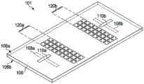
Fig. 1 is a partial perspective view of a rotational transition based clock device having a dipolar molecular vapor cell and associated transceiver circuitry for providing a reference clock signal.
Fig. 2 is a simplified diagram of the three modes of rotation of dipolar water molecules.
Fig. 3 is a graph of the rotational modes of various gases as a function of frequency with high relative absorption for low pressure water vapor at an identifiable quantum transition frequency.
FIG. 4 is a graph of transmission coefficient through a chamber versus interrogation frequency for different pressure levels within the chamber.
Figure 5 is a flow chart of a method of fabricating a vapor chamber.
FIG. 6 is a partial side view of a first substrate undergoing an etching process to form a cavity.
FIG. 7 is a partial side view of a first substrate undergoing a deposition operation to form conductive material on the bottom and sidewalls of the cavity.
Fig. 8 is a perspective view of a first substrate having a conductive interior cavity surface.
Fig. 9 is a partial side view of a second substrate undergoing a deposition process to form a conductive material on a bottom side thereof.
Fig. 10 is a partial side view of a second substrate undergoing an etching process to form a non-conductive hole through the conductive material on the bottom side.
Fig. 11 is a partial side view of a second substrate undergoing a deposition process to form a conductive material on a top side thereof.
Fig. 12 is a partial side view of a second substrate undergoing an etch process to form first and second conductive coupling structures and an electronic bandgap structure on a top side.
Fig. 13 is a partial side view of a second substrate prior to bonding with the first substrate.
Fig. 14 is a perspective view of a second substrate prior to bonding with the first substrate.
Figure 15 is a partial side view of first and second substrates undergoing a wafer bonding process to seal a cavity in a controlled low pressure environment and provide a chip scale vapor cell with dipolar molecular gas within the sealed cavity.
Figure 16 is a top view of a vapor chamber having an electromagnetic field within the cavity.
Figure 17 is a top view of another vapor chamber having non-linear cavities.
FIG. 18 is a partial perspective view of another rotational transition based atomic clock device having a plurality of non-conductive apertures and associated conductive coupling structures.
Detailed Description
In the drawings, like reference numerals refer to like elements throughout, and the various features are not necessarily drawn to scale. Novel, compact, energy efficient rotational transition clock systems and simple low cost packaging and manufacturing processes can be employed to facilitate the implementation of wafer-level or chip-level rotational spectroscopy cells or vapor cells in silicon-based processes for atomic clocks and other applications. Dipolar gas molecules (e.g. water or H)2O) have defined quantum spin state transitions, and when transitioning between spin states, such molecules absorb energy at a very repeatable frequency. For example, water absorption is based on the energy of a quantum spin state transition at 183.31 GHz. In at least one example, the clock apparatus 100 includes a vapor cell 101 fabricated in a silicon-based process that does not require lasers, modulators, photodetectors and other optical components and associated temperature-stabilizing (e.g., heating) components, as sometimes used in conventional electronic transition-based atomic clocks. Furthermore, the on-chip vapor cell 101 may be combined or interconnected with simple transceiver circuitry to implement a cost-effective and power-efficient transition-based atomic clock that can operate at a much lower frequency than electronic transition atomic clock designs that use a single, relatively simple control loop, thereby mitigating the complex control techniques of conventional atomic clock architectures.
Fig. 1 shows a clock apparatus or system 100 that includes a vapor cell structure 101, referred to herein as a physical cell, formed in this example by first and second substrates 102 and 106. The chamber 101 contains a chamber or cavity 103 having a gas (e.g., water (H)) enclosing a dipolar molecular material2O)) or any other dipolar molecular gas at a relatively low gas pressure within the cavity 103. Examples of suitable electric dipole material gases include water, acetonitrile (CH)3CN) and Hydrogen Cyanide (HCN). As shown in fig. 1, the clock 100 further includes a transmission output 1 having a function for providing an electrical transmission signal (TX) to the vapor cell 10133, and a receiver input 138 for receiving an electrical input signal (RX) from the vapor cell 101. Unlike the electronic transition vapor cell, the rotational transition vapor cell structure 101 does not require optical interrogation, but rather operates by electromagnetic interrogation via transmission and reception signaling TX, RX provided by the transceiver 130.
The sealed cavity 103 includes a conductive interior cavity surface, and first and second non-conductive holes 108a and 108b formed in the interior cavity surface for providing an electromagnetic field entrance and an electromagnetic field exit, respectively. In one example, the aperture 108 is magnetically coupled into the TE10 mode of the waveguide cavity 103. In other examples, the aperture 108 excites higher order modes. A first conductive coupling structure 110a is formed on the outer surface 106a of the vapor cell 101 proximate to the first non-conductive aperture 108 a. In the example 100, the first coupling structure 110a is a conductive strip formed on the upper surface 106a of the upper substrate 106 that overlies (e.g., and traverses) the corresponding first non-conductive aperture 108a to provide an electromagnetic interface to couple a magnetic field into the interior of the cavity 103 based on the transmission signaling TX from the transceiver output 133. A second coupling structure 110b is formed proximate the second non-conductive aperture 108b for providing an electromagnetic field exit from the cavity 103 to couple an electromagnetic field with the transceiver RX input 138. The proximate location of the conductive coupling structure 110 and the corresponding non-conductive via 108 advantageously provides an electromagnetic transmission path through the second or upper substrate 106, which may be any electromagnetic transmission material. In some examples, one or more conductive Electronic Bandgap (EBG) structures 120 are formed on the outer surface 106a of the vapor cell 101, spaced apart from the conductive coupling structure 110. In operation, the EBG structures 120 attenuate electromagnetic waves coupled between the transmit and receive coupling structures 110a and 110b, respectively, along the vapor cell outer surface 106 a. In other examples, EBG structure 120 may be omitted.
The lower side 106b of the second substrate 106 is substantially or completely plated with a conductive material (e.g., copper 94 as shown in fig. 9-12 below), and the hole 108 is etched to provide a non-conductive window or hole 108 in the lower second side 106b, with the coupling structure 110 and any included EBG structures 120 formed from the conductive material (e.g., copper) on the upper side 106a of the second substrate 106. One example includes two EBG structure patterns 120a and 120b, which may be any suitable shape and configuration for electromagnetic attenuation on the upper surface 106a of the vapor cell 101. The chamber cavity 103 is defined by the underside 106b of the upper substrate 106 and by the sidewalls 104 and a cavity bottom 103b formed in the first (lower) substrate 102, which may be any suitable material, such as silicon, as shown further below in fig. 8.
In the example of fig. 1, the first or lower substrate 102 includes a top or first side 102a, with cavity sidewalls 104 and a cavity bottom 103b formed in the top or first side 102a, such as by etching (e.g., fig. 6 below). In this example, the chamber cavity 130 extends along a substantially linear axis from a first end to a second end, with the first aperture 108a proximate the first end and the second aperture 108b proximate the second end. Another example, described further below in connection with fig. 18, has more than two holes 108 formed in the cavity conductive surface.
Various different cavity sizes and shapes may be used in other examples. One suitable example provides a substantially rectangular cavity shape with a top width of about 1.5mm and an etch depth of 0.5mm, with the first mode starting at 120GHz, the second mode starting at 230GHz, and the third mode starting at 290 GHz. Other shapes, sizes, and configurations of the chamber cavity 103 are possible. For example, fig. 17 below illustrates another vapor cell example 101 having a tortuous cavity shape with a length dimension L extending along a non-linear axis from a first end proximate to a first aperture 108a to a second end proximate to a second aperture 108 b.
As shown in fig. 1, the second side 106b of the second substrate 106 is mounted to the first side 102a of the first substrate 102 to form the cavity 103. The cavity 103 includes a sealed interior with a conductive interior cavity surface extending at least partially along one or more cavity sidewalls 104, a cavity bottom 103b, and an underside 106b of a second substrate 106. The lower second side 106b of the second substrate 106 provides the conductive surface 94 (fig. 15, below) for the cavity top. In some examples, the only non-conductive cavity surface is the non-conductive hole 108 on the bottom 106b of the upper substrate 106. In some examples, other non-conductive portions are possible within the cavity 103. In the illustrated example, the conductive interior cavity surface is plated or otherwise provided with copper or other metallic material having a thickness greater than a skin depth at the frequency of the transmission output signal TX. Processing chamber with controlled low pressure environmentIn the chamber, the first and second substrates 102 and 106 are bonded together, in some examples by a wafer bonding process (e.g., fig. 15 below), to provide a dipolar molecular gas (e.g., H) in the cavity 103 during wafer bonding at a pressure of about 1 mbar or less2O). In certain examples, the dipolar molecule gas is at a low pressure of about 0.1 mbar or less and about 0.01 mbar or more within the sealed interior of the cavity 103. In general, pressure can be tailored for a given design, with the transition width being primarily dependent on pressure broadening and doppler broadening. The pressure broadening factor is linear with pressure, while the doppler broadening is constant with pressure. Thus, at one desired pressure, due to the doppler effect, further pressure reduction will not provide further transition frequency width reduction, and further pressure reduction will reduce the magnitude of the peak transition, and the widths will be the same, thereby degrading detection and transition tracking.
A getter may be introduced during wafer bonding to include the getter within the resulting vapor cavity 103 to remove any contaminants that may be present during the wafer bonding process and/or that may leak into the cavity 103 over time with the getter.
In some examples, the chamber 101 may include a pattern heater having a temperature sensor formed on or in the chamber bottom 102b for stabilizing the chamber temperature. This heating element may be operable to boil any steam absorbed on the chamber side wall 104, thereby promoting pressure stability in operation.
The transceiver circuit 130 in some implementations is implemented on or in an integrated circuit (not shown) to which the vapor cell 101 is electrically coupled to transmit TX signals via the output 133 and receive RX signals via the input 138. The transceiver 130, when powered, is operable to provide an alternating electrical output signal TX to the first conductive coupling structure 110a for coupling an electromagnetic field into the interior of the cavity 103, and to receive an alternating electrical input signal RX from the second conductive coupling structure 110b representative of the electromagnetic field received from the cavity 103. The transceiver circuitry 130 is operable to: (a) selectively adjusting the frequency of electrical output signal TX to reduce electrical input signal RX by interrogation to operate clock 100 at a frequency that substantially maximizes molecular absorption by rotating motor state transitions; and (b) provide a reference clock signal REFCLK to clock circuit 140 at the frequency of the TX output signal.
In some examples, the transceiver 130 includes a signal generator 132, wherein an output 133 is electrically coupled with the first electrically conductive coupling structure 110a for providing the alternating electrical output signal TX and for providing the reference clock signal REFCLK at the corresponding transmission output frequency. Transceiver 130 also includes a lock-in amplifier circuit 134, with input 138 coupled with second conductive coupling structure 110b for receiving the RX signal, and the lock-in amplifier is operative to provide an error signal ERR representing a difference between the RX signal and electrical output signal TX. In one example, the error signal ERR is provided as an in-phase output by the lock-in amplifier circuit 134 and is used as an input to a loop filter or controller circuit 136 for providing a control output signal CO to the signal generator 132 for selectively adjusting the TX output signal frequency to maintain this frequency at the peak absorption frequency of the dipolar molecular gas within the sealed interior of the cavity 103. In some examples, the RF power of the TX and RX loops is controlled to avoid or mitigate severe offset effects.
The electromagnetic coupling via the non-conductive apertures 108 and the corresponding conductive coupling structures 110 facilitates electromagnetic interrogation of the dipolar gas within the chamber cavity 103, and the system 100 avoids the cost, complexity, power consumption, and optical transmission issues associated with conventional electronic transition atomic clock vapor cells. In one form of operation, the clock system 100 operates with the signal generator 132, the signal generator 132 transmitting the alternating signal TX at full transmission power at various frequencies within a defined frequency band around the suspected quantum absorption frequency at which the transmission efficiency of the vapor cell 101 is minimal (absorption is maximal). For example, the quantum absorption frequency associated with dipolar water molecules is 183.31 GHz. When the system is operating at a quantum frequency, a zero or minimum value is detected at the receiver via lock-in amplifier 134, and lock-in amplifier 134 provides error signal ERR to loop filter 136 for adjusting the TX output signal frequency via the control output CO signal provided to signal generator 132. The rotational quantum frequency of the dipolar molecular gas in the vapor chamber cavity 103 is generally stable with respect to time (does not degrade or drift over time) and is largely independent of temperature and a number of other variables. Thus, the clock system 100 need not include thermal or other stabilizing circuitry found in atomic clocks based on electronic transitions.
In one example, the transceiver system 130 operates the signal generator 132 to initially sweep the transmission output frequency through a frequency band known to contain the quantum frequency of the chamber 101 (e.g., shift up from the initial frequency to below the suspect quantum frequency, or initially transition down from an initial frequency higher than the suspect quantum frequency, or other suitable sweeping technique or method). The transceiver circuitry 130 monitors the received energy via an input 138 coupled with (e.g., electrically connected to) the second conductive coupling structure 110b to identify a transmission frequency (e.g., minimum reception at a receiver) associated with peak absorption by the gas in the chamber cavity 103. After identifying the quantum absorption frequency, the loop filter or controller 136 brings the source signal generator transmission frequency close to the absorption frequency (e.g., 183.31GHz) and modulates the signal at a very low frequency (e.g., left and right along the frequency axis in fig. 4) to adjust operation around the zero or minimum in transmission efficiency representing the ratio of received energy to transmitted energy, where the loop filter 136 provides negative feedback in closed loop operation to maintain the signal generator 132 operating at the TX frequency corresponding to the quantum frequency of the cavity dipolar molecular gas.
Unlike the electronic transition type atomic clock using optical interrogation of alkali metal gas vapor cells, the disclosed rotational transition based atomic clock 100 uses the rotational transition of dipolar molecules (e.g., water), with the frequency of this type of quantum transition in the sub-THz range. In this regard, while the electronic transition type atomic clock requires a laser operating at hundreds of THz (wavelengths of hundreds of nanometers) to excite an alkali metal gas, the millimeter wave clock 100 interrogates the gas with millimeter wave radiation induced by the RF transceiver circuit 130. In some examples, clock 100 may be locked to a rotating quantum molecular transition, with typical Allen (Alan) biases of 1e-10 to 1e-11 averaging 100 seconds. In some examples, the disclosed rotational transition based atomic clock apparatus 100 operates at sub-THz frequencies and is therefore a simpler, lower cost, and lower power solution for providing a stable reference clock signal.
In steady state operation, the lock-in amplifier 134 and loop filter 136 maintain the transmitter frequency at the peak absorption frequency of the chamber gas. In one example, the loop filter 136 uses the derivative of the frequency error to provide PID control as a control factor for lock detection and closed loop regulation. At the bottom of the zero point of the transmission coefficient curve of fig. 4, the derivative is zero and the loop filter 136 feeds the derivative back to the signal generator 132 as the DC control output signal CO. This closed loop operates to maintain the signal generator transmission output frequency at the peak absorption frequency of the chamber gas using lock-in discrimination based on the RX signal received from the chamber 101. As shown in fig. 1, another clock circuit 140 receives a reference clock signal REFCLK for use by a frequency divider to generate a system clock in a host system (not shown).
Referring also to fig. 2-4, fig. 2 provides diagrams 200, 202 and 204 showing three modes of rotation of dipolar water molecules along three orthogonal axes, respectively, and fig. 3 shows a graph 300 of the relative absorption of the modes of rotation of various gases as a function of electromagnetic wave frequency. As shown in FIG. 3, the absorption line 302 corresponding to water indicates this dipolar molecule H2O has a high relative absorption for low pressure water vapor at an identifiable quantum transition frequency (183.31GHz) and a much higher absorption than the residual gas at the same frequency range.
Fig. 5-15 show wafer-level or chip-level fabrication techniques by which the vapor cell 101 and atomic clock system 100 can be produced using silicon or other semiconductor-based integrated circuit processes for compact, low power, and cost-effective solutions. Figure 5 shows a process or method 500 for fabricating a vapor cell 101, where various interconnect techniques may be used to subsequently integrate the produced vapor cell 101 with a transceiver circuit 130 to provide the clock system 100, and figures 6-15 show the cell 101 at various stages of the fabrication process according to the method 500. The example process 500 facilitates packaging a compact chip-scale vapor cell 101 or physical cell with a low-pressure dipolar molecule gas directly in the millimeter wave waveguide cavity 103, which may be packaged with the transceiver die via wire bonding, flip chip, or other packaging techniques.
The process 500 in fig. 5 begins at 502 with the formation of a cavity 103 in a first (e.g., top) side 102a of a first substrate 102. In one example, the first substrate is a silicon wafer. Other substrate materials may be used for different examples, such as glass. Any suitable wet or dry etch process 602 (as shown in fig. 6) may be used for cavity formation at 502 in fig. 5. In some examples, multiple cavities 103 may be formed in a single substrate 102, such as for creating multiple vapor cells 101, with final die separation for separating individual vapor cells 101 from each other (at 514 in fig. 5). As shown in fig. 6, the shape of the cavity 103 is formed at 502 by patterning using a hard mask 604. In other examples, a polymer resist may be used that is specifically formulated to resist etchants (e.g., Brewer Science ProTek series of resists) as well as bulk anisotropic etching of the silicon substrate 102 via process 602, such as using a strongly basic etchant (e.g., KOH or TMAH).
The etch process 602 forms at least one sidewall 104 with the cavity bottom 103b having a substantially smooth surface, in some examples, the process 602 provides a cavity bottom and sidewall roughness below about 5 μm RMS for reducing electromagnetically induced current loss in operation of the vapor cell 101. In another example, the etch process 602 etches through the silicon substrate 102 down to a buried etch stop layer (not shown), which may be formed by bonding a first substrate comprising silicon directly to a second substrate (not shown), which may be silicon or another material such as glass, with a dielectric layer (e.g., silicon dioxide or silicon nitride) therebetween. This direct bonding can be achieved by several wafer bonding methods, one example of which uses low temperature plasma activated fusion bonding to achieve the lowest cost and high throughput. After the cavity formation at 502 in fig. 5 and the etch process 602 in fig. 6, any desired mask 604 is removed and a cleaning process may be performed.
In some examples, dielectric layers may be formed on the cavity walls 104 and on the cavity bottom 103b for enhancing adhesion of subsequently deposited metal materials using any suitable deposition process (e.g., vapor deposition, sputtering, Chemical Vapor Deposition (CVD), Atomic Layer Deposition (ALD), etc.), one of which is tantalum pentoxide (Ta) for good adhesion to copper2O5)。
At 504 in FIG. 5, a conductive material 904 is formed directly on the sidewalls 104 and cavity bottom 103b or over any deposited dielectric layer using any suitable deposition process 702 as shown in FIG. 7. Fig. 8 shows the resulting first substrate 102 following the conductive material deposition process 702 of fig. 7, wherein conductive material is formed on the sidewalls 104, cavity bottom 103b, and top side 102a of the first substrate 102. In one example, the deposited conductive material is copper, and the surface roughness is about 100nm or less for minimizing losses due to currents induced by electromagnetic fields within the cavity 103.
One suitable deposition process 702 is to sputter copper metal onto the deposited dielectric layer to provide high conductivity without remote magnetic ordering, versus Ta2O5Good adhesion and low cost. Other metallic materials may be used in different examples, such as examples having similar combination of properties. After sputter deposition in one embodiment, the metal layer may be grown to a desired uniform thickness with copper or any other metal that may be desired (e.g., using electroplating to reduce deposition costs). In some examples, the formed metal layer may be coated with a dielectric material via vapor deposition or other suitable process, wherein the optional dielectric material in some examples may be selected to mitigate reaction of vapor phase molecules of the vapor chamber 101 with the metal layer during the expected product lifetime. Any included dielectric may be removed by patterning and etching all or a target bonding portion of the top surface 102a of the first substrate 102 to facilitate bonding with the second substrate 106 to close the cavity 103, as described further below. In this example, at 504 in figure 5, a conductive material is formed on the sidewalls 104 and cavity bottom 103b to a thickness greater than the skin depth at the operating frequency of the finished vapor cell 101, such as about 100nm or more and about 1 μm or less to provide a surface roughness of about 50nm or less for mitigating signal loss in the cavity 103 in one example.
At 506 in fig. 5, a second substrate 106 having a first or top side 106a and a second or bottom side 106b is provided. A conductive material 904 is formed on the bottom side 106b of the second substrate 106 using a deposition process 902 as shown in fig. 9. The second substrate 106 will be used later to form the cavity top by bonding with the first substrate 102 and may be any suitable material, such as a thickness having a wavelength less than the vapor cell operating frequency (e.g., atIn one example less than 0.5 mm). In practice it is suitable that the second substrate 106 is sufficiently thin to promote good electromagnetic coupling of microwave energy through the aperture 108 to the cavity 103, or good electromagnetic coupling through the aperture 108 away from the cavity 103, and sufficiently thick to mitigate or avoid structural distortion when bonded to the first substrate 102 to seal the cavity 103 under vacuum. In this regard, the second substrate material preferably provides good electromagnetic transmissivity through subsequently patterned non-conductive apertures 108 formed in the material 904, as described below. One suitable example material is Corning Eagle XG glass, a useful low alkali borosilicate glass having a wafer thickness in the range of 0.2 to 3.0 mm. In some examples, the second substrate 106 is coated with a dielectric (e.g., Ta) on each side 106a and 106b2O5) To improve adhesion of a metal film that is later formed over the dielectric.
As shown in fig. 9-13, the first and second sides 106a and 106b may be separately deposited and patterned of conductive material. In one alternative example, the top and bottom sides 106a and 106b may be fully metalized in one step, followed by subsequent selective patterning to leave desired conductive and non-conductive areas on both sides 106a and 106 b. In the illustrated example, the bottom side 106b is etched at 508 of fig. 5 using a mask 1004 as shown in fig. 10 via an etch process 1002 to form first and second spaced holes 108a and 108b, respectively, through the conductive material 904 on the bottom side 106b, with the remainder of the bottom side 106b remaining coated with the conductive material 904. These holes or slots 108 form part of an electromagnetic coupling structure that will allow the electromagnetic field to enter or exit the cavity 103 in the finished vapor cell 101, as described above in connection with fig. 1.
Continuing at 510 in fig. 5, first and second conductive coupling structures 110a and 110b are formed on the first side 106a of the second substrate 106 proximate to corresponding apertures 108a and 108b formed along the bottom side 106b, as shown in fig. 11-14. In fig. 11, a deposition process 1102 is used to plate the first side 106a with copper or other suitable conductive material 1104, and an etch process 1202 is used with an etch mask 1204 in fig. 12 to form the first and second copper coupling structures 110a and 110b shown in fig. 13. As further shown in fig. 14, the conductive coupling structures 110a and 110b in one example are formed as conductive strips that extend longitudinally across the underlying apertures 108a and 108b, respectively, for electromagnetic coupling with the interior of the waveguide cavity 103. In subsequent packaging with the host transceiver 130 (e.g., fig. 1), the coupling structure 110 may be electrically coupled with the inputs 133 and 138 using any suitable flip-chip, wire bonding, or other electrical interconnection technique to provide a simple and cost-effective package assembly in which the finished vapor chamber structure 101 is mounted to a host integrated circuit package or printed circuit board (not shown). In operation, the first coupling structure 110a receives the transmission signal TX from the output 133 of the transceiver 130 and generates a magnetic field that is directed through the aperture 108a to the dipolar molecular gas within the sealed cavity 103.
As further shown in fig. 12-14, this example also includes a patterned conductive Electronic Bandgap (EBG) structure 120 (fig. 13 and 14) formed on the outer surface 106a of the vapor cell 101 via the etch mask 1204 in fig. 12, wherein the EBG structure 120 is spaced from the conductive coupling structure 110 to avoid or mitigate propagation of stray surface waves. In the example of fig. 14, the first and second EBG structures 120a and 120b each comprise three rows of several repeating patterns of conductive material 1104, wherein any suitable pattern may be used to attenuate electromagnetic waves coupled along the first side 106a of the second substrate 106 for frequencies of a given target bandgap range, wherein the EBG structures 120 are spaced apart from the transmit and receive coupling structures 110a and 110b and disposed between the transmit and receive coupling structures 110a and 110 b. In other examples, only a single EBG structure 120 is used, spaced from the coupling structures 110a and 110b and between the coupling structures 110a and 110 b. Other possible examples include more than two EBG structures 120 for attenuating electromagnetic genetic waves coupled along the first side 106 a. EBG structure 120 is omitted in other embodiments.
As shown in the example second substrate 106 of fig. 14, the aperture 108 and the coupling structure 110 are both elongated rectangular shapes, although other shapes and relative positions may be used in other examples. In various examples, the aperture 108 may be perpendicular or parallel to the direction of propagation of the TE01 mode within the cavity 103. Because the transceiver circuit 130 provides a high frequency TX signal (e.g., 100 to 1000GHz in various examples) to the vapor cell 101, and because the second substrate 106 has a thickness of a fraction of a wavelength in some examples, surface waves can propagate along a grounded dielectric slab or along the top surface 106a of the cell 101 and couple between the input and output apertures 108 of the waveguide, thereby creating a second path for the signal that does not travel through the vapor cell cavity 103, and further the cavity transmission can mask absorption of the dipolar molecular gas within the cavity 103 in operation.
Thus, some examples include one or more EBG structures 120 that mitigate such surface waves by operating as photonic bandgap structures. In one example, the EBG structure 120 has a bandgap in the expected operating range of frequencies to mitigate or prevent surface wave propagation, tuned into the frequency range used to interrogate the vapor cell 101. An EBG is a tuned filter that includes a parallel combination of a conductive layer 904 on the second or bottom side 106b of the second substrate 106 and a patterned array of repeating unit cells 120 on the first or top side 106 a. In the illustrated example, no vias are required, but vias may be used in other examples. In one example, the waveguide cavity 103 is etched with a top width of 1.5mm and an etch depth of 0.5mm to provide the propagation constant and cutoff for the first three modes, with a first mode starting at 120GHz, a second mode starting at 230GHz, and a third mode starting at 290GHz, and the cavity 103 is designed in one example for operation in a frequency range where only the first mode can propagate (which can be tuned by changing the waveguide dimensions in other examples). In this example, there is a bandgap ranging in frequency from 160 to 195GHz where no mode can propagate along the top side 106a, with the EBG array 120 placed between the two ports of the waveguide to prevent a second path for electromagnetic signals in the bandgap of interest.
Continuing at 512 in fig. 5, the bottom side 106b of the second substrate 106 is bonded to the first side 102a of the first substrate 102 via the bonding process 1500 of fig. 15 in an ambient environment containing a dipolar molecule gas at a low ambient pressure to form a substrate containing a low-pressure dipolar molecule gas H2O, sealed chamber 103. The bonding process 1500 may be any suitable wafer bonding step that does not introduce any undesired gases within the cavity 103 and seals the cavity 103 with a low pressure dipolar molecule vapor. Of a suitable metalExample bonding process 1500 involves the formation of solid-liquid interdiffusion (SLID) bonds or Transient Liquid Phase (TLP) bonds, for example, formed at a lower temperature and having a higher re-melting temperature than the temperature at which they were formed. Common TLP bonding metal pairs include Au/In, Cu/Sn, Sn/Au, Sn/Ag, where the metal pairs may be selected for convenience and overall compatibility with the final device geometry. In certain examples, the cavity pressure is in the range of micro-torr to millitorr, and thus the substrates 102 and 106 are bonded and sealed at 512 in a processing chamber capable of providing and controlling both heat and vacuum. Suitable processing chambers for the bonding process 1500 are available from suppliers such as Electronic Vision Group (EVG), Austria. Substrates 102 and 106 are placed in a chamber and a suitable vacuum headspace is established with a desired partial pressure of dipolar molecular vapor (water, acetonitrile, or methyl fluoride). The substrates 102 and 106 are then bonded according to a corresponding suitable temperature profile for creating an impermeable seal for each separated chamber 103 of the processed wafer, wherein all chambers are bonded substantially simultaneously at the wafer level. In an alternative implementation, the cavity 103 may be sequentially sealed by an apparatus that uses laser radiation to locally heat the bonding area to a suitable temperature while maintaining a lower temperature of the surrounding die to mitigate degradation and loss of volatile species.
At 514 in fig. 5, the device containing the desired concentration of low-pressure dipolar molecule gas is snapped using a suitable semiconductor dicing technique. The finished vapor chamber 101 (physical chamber) may then be used for further processing, such as pick and place or bonding via wires to other microwave devices for connection of a fully integrated system solution.
Figure 16 shows a simplified top view of the finished single vapor cell device 101 in operation via the associated transceiver circuitry 130 (e.g., figure 1) during interrogation. The alternating electrical output signal TX is provided to the first electrically conductive coupling structure 110a via the transceiver output 133 for coupling the electromagnetic field 1600 to the interior of the cavity 103 via the input aperture 108 a. The field 1600 extends along the longitudinal length L of the cavity 103 to the exit aperture 108b to provide an alternating electrical input signal RX to the transceiver input 138 via the second coupling structure 110 b. As mentioned above, the finished vapor cell 101 may include one or more EBG structures 120 (e.g., fig. 1) disposed along the top side of the cell structure 101 for attenuating electromagnetic waves, which are omitted from fig. 16 for ease of illustration of the electromagnetic field 1600 within the interior of the cavity 103.
Figure 17 shows another vapor cell example 101 constructed using the principles described in detail above, where the cell cavity meanders along a non-linear path to increase length, and thus increase absorption to provide a compact device 101, where the absorption length L in figure 11 is longer than the length of the cell 101 in figure 16, despite the shorter overall length of the cell structure 101. Other examples are possible including chamber cavities 103 extending along linear or non-linear paths including combinations of linear and non-linear portions, curvilinear portions, stepwise linear portions, and combinations thereof, although example embodiments are not limited to the illustrated examples.
Figure 18 illustrates another vapor cell example 101 in which cavity 103 includes third and fourth conductive vias 108c and 108d, each conductive coupling structure 110 proximate to a pair of non-conductive vias. In this example, the apertures 108a and 108c are parallel to each other and the corresponding transmission coupling structure 110a extends substantially perpendicularly across a pair of parallel apertures 108a and 108 c. Similarly, the non-conductive bottom side apertures 108b and 108d are substantially parallel to each other with the associated receiving conductive coupling structure 110b extending perpendicular to or over the corresponding receiver apertures 108b and 108 d. In this example, the third aperture 108c provides a second electromagnetic field entrance to the cavity 103 and the fourth non-conductive aperture 108d provides another electromagnetic field exit from the cavity 103. In other examples, other combinations of one or more apertures 108 and one or more associated conductive coupling structures 110 may be used for electromagnetic coupling with the interior of the cavity 103.
Thus, example embodiments provide a millimeter-wave atomic clock 100 and a rotating transition vapor cell 101, thus providing simple cost-effective and low-power operation of the reference clock signal REFCLK using rotating quantum transitions of low-pressure gas molecules, while avoiding the complexity, power consumption, cost, and size drawbacks of conventional atomic clocks that use electronic transitions to establish a reference. The disclosed atomic clock concept based on rotational transitions is stable with respect to temperature variations and can be fabricated using chip-level or wafer-level processing techniques. Furthermore, the disclosed clock 100 operates at a much lower frequency than electronic transition devices to determine and lock the rotational quantum states of low-pressure dipolar molecule vapors, and the disclosed techniques avoid problems associated with providing a clear optical transmission path as in conventional optical interrogation vapor cells. Furthermore, the disclosed vapor cell 101 may be used in various low-cost millimeter wave CMOS transceiver circuits 130 to interrogate low-pressure dipolar molecule gases in the physical cell 101 over a bandwidth covering the transition. Furthermore, water and other dipolar molecular gases exhibit detectable changes in absorption at the transition frequency to facilitate locking to provide a stable reference clock signal, and in some examples the vapor cell 101 and the entire atomic clock system 100 may be constructed and packaged within a silicon fabrication and packaging process. Furthermore, the disclosed chip-scale dipolar molecule vapor cell 101 may be used in atomic clocks and other applications involving rotational spectroscopy, and provides a more compact design than other rotational spectroscopy solutions.
In the described embodiments, modifications are possible, and other embodiments are possible within the scope of the claims.
Claims (15)
1. A clock apparatus, comprising:
a vapor chamber, comprising:
a cavity including a sealed interior having a conductive interior cavity surface, a first non-conductive aperture in the interior cavity surface for providing an electromagnetic field entrance to the cavity, and a second non-conductive aperture in the interior cavity surface spaced from the first non-conductive aperture for providing an electromagnetic field exit from the cavity,
a dipolar molecular gas within the sealed interior of the cavity,
a first conductive coupling structure formed on an outer surface of the vapor cell proximate to the first non-conductive hole, an
A second conductive coupling structure formed on the outer surface of the vapor cell proximate to the second non-conductive hole; and
a transceiver circuit for providing an alternating electrical output signal to the first electrically conductive coupling structure for coupling an electromagnetic field to the interior of the cavity, for receiving an alternating electrical input signal from the second electrically conductive coupling structure representing the electromagnetic field received from the cavity, for selectively adjusting a frequency of the electrical output signal to reduce the electrical input signal, and for providing a reference clock signal at the frequency of the electrical output signal; wherein
The cavity extends along a non-linear axis from a first end to a second end, wherein the first non-conductive aperture is proximate the first end, and wherein the second non-conductive aperture is proximate the second end.
2. A clock apparatus, comprising:
a vapor chamber, comprising:
a cavity including a sealed interior having a conductive interior cavity surface, a first non-conductive aperture in the interior cavity surface for providing an electromagnetic field entrance to the cavity, and a second non-conductive aperture in the interior cavity surface spaced from the first non-conductive aperture for providing an electromagnetic field exit from the cavity,
a dipolar molecular gas within the sealed interior of the cavity,
a first conductive coupling structure formed on an outer surface of the vapor cell proximate to the first non-conductive hole, an
A second conductive coupling structure formed on the outer surface of the vapor cell proximate to the second non-conductive hole; and
a transceiver circuit for providing an alternating electrical output signal to the first electrically conductive coupling structure for coupling an electromagnetic field to the interior of the cavity, for receiving an alternating electrical input signal from the second electrically conductive coupling structure representing the electromagnetic field received from the cavity, for selectively adjusting a frequency of the electrical output signal to reduce the electrical input signal, and for providing a reference clock signal at the frequency of the electrical output signal;
wherein the cavity includes a third non-conductive aperture spaced from the first non-conductive aperture in the interior cavity surface for providing another electromagnetic field entrance to the cavity, and a fourth non-conductive aperture spaced from the second non-conductive aperture in the interior cavity surface for providing another electromagnetic field exit from the cavity; wherein the first conductive coupling structure is proximate to the first and third non-conductive vias; and wherein the second conductive coupling structure is proximate to the second and fourth non-conductive vias.
3. A clock apparatus, comprising:
a vapor chamber, comprising:
a cavity including a sealed interior having a conductive interior cavity surface, a first non-conductive aperture in the interior cavity surface for providing an electromagnetic field entrance to the cavity, and a second non-conductive aperture in the interior cavity surface spaced from the first non-conductive aperture for providing an electromagnetic field exit from the cavity,
a dipolar molecular gas within the sealed interior of the cavity,
a first conductive coupling structure formed on an outer surface of the vapor cell proximate to the first non-conductive hole, an
A second conductive coupling structure formed on the outer surface of the vapor cell proximate to the second non-conductive hole; and
a transceiver circuit for providing an alternating electrical output signal to the first electrically conductive coupling structure for coupling an electromagnetic field to the interior of the cavity, for receiving an alternating electrical input signal from the second electrically conductive coupling structure representing the electromagnetic field received from the cavity, for selectively adjusting a frequency of the electrical output signal to reduce the electrical input signal, and for providing a reference clock signal at the frequency of the electrical output signal;
at least one conductive electronic bandgap structure formed on the outer surface of the vapor cell spaced from and between the first and second conductive coupling structures for attenuating electromagnetic waves coupled along the outer surface of the vapor cell.
4. A clock apparatus, comprising:
a vapor chamber, comprising:
a cavity including a sealed interior having a conductive interior cavity surface, a first non-conductive aperture in the interior cavity surface for providing an electromagnetic field entrance to the cavity, and a second non-conductive aperture in the interior cavity surface spaced from the first non-conductive aperture for providing an electromagnetic field exit from the cavity,
a dipolar molecular gas within the sealed interior of the cavity,
a first conductive coupling structure formed on an outer surface of the vapor cell proximate to the first non-conductive hole, an
A second conductive coupling structure formed on the outer surface of the vapor cell proximate to the second non-conductive hole; and
a transceiver circuit for providing an alternating electrical output signal to the first electrically conductive coupling structure for coupling an electromagnetic field to the interior of the cavity, for receiving an alternating electrical input signal from the second electrically conductive coupling structure representing the electromagnetic field received from the cavity, for selectively adjusting a frequency of the electrical output signal to reduce the electrical input signal, and for providing a reference clock signal at the frequency of the electrical output signal;
wherein the transceiver circuit comprises:
a signal generator having an output electrically coupled with the first conductive coupling structure for providing the alternating electrical output signal to the first conductive coupling structure and providing the clock signal at the frequency of the electrical output signal;
a lock-in amplifier having an input electrically coupled to the second conductive coupling structure for receiving the alternating electrical input signal and providing an error signal representative of a difference between the electrical input signal and the electrical output signal; and
a loop filter for receiving the error signal and providing a control output signal to the signal generator for selectively adjusting the frequency of the electrical output signal to maintain the frequency of the electrical output signal at a peak absorption frequency of the dipolar molecular gas within the sealed interior of the cavity.
5. A clock apparatus, comprising:
a vapor chamber, comprising:
a cavity including a sealed interior having a conductive interior cavity surface, a first non-conductive aperture in the interior cavity surface for providing an electromagnetic field entrance to the cavity, and a second non-conductive aperture in the interior cavity surface spaced from the first non-conductive aperture for providing an electromagnetic field exit from the cavity,
a dipolar molecular gas within the sealed interior of the cavity,
a first conductive coupling structure formed on an outer surface of the vapor cell proximate to the first non-conductive hole, an
A second conductive coupling structure formed on the outer surface of the vapor cell proximate to the second non-conductive hole; and
a transceiver circuit for providing an alternating electrical output signal to the first electrically conductive coupling structure for coupling an electromagnetic field to the interior of the cavity, for receiving an alternating electrical input signal from the second electrically conductive coupling structure representing the electromagnetic field received from the cavity, for selectively adjusting a frequency of the electrical output signal to reduce the electrical input signal, and for providing a reference clock signal at the frequency of the electrical output signal;
wherein the vapor chamber includes: a first substrate comprising a first side, at least one cavity sidewall extending inward from the first side, and a cavity bottom; and a second substrate including a first side and a second side including a cavity top, the second side of the second substrate mounted to the first side of the first substrate to form the cavity including the sealed interior having the conductive interior cavity surface extending at least partially along the at least one cavity sidewall, the cavity bottom, and the second side of the second substrate;
wherein the first and second non-conductive apertures are formed in the interior cavity surface on the second side of the second substrate for providing the electromagnetic field entrance and exit, respectively; and is
Wherein the first and second conductive coupling structures are formed on the first side of the second substrate.
6. A clock apparatus, comprising:
a vapor chamber, comprising:
a cavity including a sealed interior having a conductive interior cavity surface, a first non-conductive aperture in the interior cavity surface for providing an electromagnetic field entrance to the cavity, and a second non-conductive aperture in the interior cavity surface spaced from the first non-conductive aperture for providing an electromagnetic field exit from the cavity,
a dipolar molecular gas within the sealed interior of the cavity,
a first conductive coupling structure formed on an outer surface of the vapor cell proximate to the first non-conductive hole, an
A second conductive coupling structure formed on the outer surface of the vapor cell proximate to the second non-conductive hole; and
a transceiver circuit for providing an alternating electrical output signal to the first electrically conductive coupling structure for coupling an electromagnetic field to the interior of the cavity, for receiving an alternating electrical input signal from the second electrically conductive coupling structure representing the electromagnetic field received from the cavity, for selectively adjusting a frequency of the electrical output signal to reduce the electrical input signal, and for providing a reference clock signal at the frequency of the electrical output signal;
wherein the dipolar molecular gas is at a pressure of about 1 mbar or less within the sealed interior of the cavity.
7. The clock device of claim 6, wherein the dipolar molecule gas is at a pressure of about 0.1 mbar or less within the sealed interior of the cavity; and wherein the dipolar molecule gas is at a pressure of about 0.01 mbar or greater within the sealed interior of the cavity.
8. A clock apparatus, comprising:
a vapor chamber, comprising:
a cavity including a sealed interior having a conductive interior cavity surface, a first non-conductive aperture in the interior cavity surface for providing an electromagnetic field entrance to the cavity, and a second non-conductive aperture in the interior cavity surface spaced from the first non-conductive aperture for providing an electromagnetic field exit from the cavity,
a dipolar molecular gas within the sealed interior of the cavity,
a first conductive coupling structure formed on an outer surface of the vapor cell proximate to the first non-conductive hole, an
A second conductive coupling structure formed on the outer surface of the vapor cell proximate to the second non-conductive hole;
a first substrate comprising a first side, at least one cavity sidewall extending inward from the first side, and
a cavity bottom; and
a second substrate including a first side and a second side including a cavity top, the second side of the second substrate mounted to the first side of the first substrate to form the cavity including the sealed interior having the conductive interior cavity surface extending at least partially along the at least one cavity sidewall, the cavity bottom, and the second side of the second substrate;
a transceiver circuit for providing an alternating electrical output signal to the first electrically conductive coupling structure for coupling an electromagnetic field to the interior of the cavity, for receiving an alternating electrical input signal from the second electrically conductive coupling structure representing the electromagnetic field received from the cavity, for selectively adjusting a frequency of the electrical output signal to reduce the electrical input signal, and for providing a reference clock signal at the frequency of the electrical output signal;
wherein the conductive interior cavity surface is plated with a metal material extending at least partially along the at least one cavity sidewall, the cavity bottom, and the second side of the second substrate, the metal material having a thickness greater than a skin depth at the frequency of the electrical output signal.
9. A vapor chamber, comprising:
a cavity formed in at least one substrate, the cavity including a sealed interior having a conductive interior cavity surface, a first non-conductive aperture in the interior cavity surface for providing an electromagnetic field entrance to the cavity, and a second non-conductive aperture in the interior cavity surface spaced from the first non-conductive aperture for providing an electromagnetic field exit from the cavity;
a dipolar molecular gas within the sealed interior of the cavity,
a first conductive coupling structure formed on an outer surface of the vapor cell proximate to the first non-conductive hole, an
A second conductive coupling structure formed on the outer surface of the vapor cell proximate to the second non-conductive hole; wherein the cavity extends along a non-linear axis from a first end to a second end, wherein the first non-conductive aperture is proximate the first end, and wherein the second non-conductive aperture is proximate the second end.
10. A vapor chamber, comprising:
a cavity formed in at least one substrate, the cavity including a sealed interior having a conductive interior cavity surface, a first non-conductive aperture in the interior cavity surface for providing an electromagnetic field entrance to the cavity, and a second non-conductive aperture in the interior cavity surface spaced from the first non-conductive aperture for providing an electromagnetic field exit from the cavity;
a dipolar molecular gas within the sealed interior of the cavity,
a first conductive coupling structure formed on an outer surface of the vapor cell proximate to the first non-conductive hole, an
A second conductive coupling structure formed on the outer surface of the vapor cell proximate to the second non-conductive hole;
wherein the cavity includes a third non-conductive aperture spaced from the first non-conductive aperture in the interior cavity surface for providing another electromagnetic field entrance to the cavity, and a fourth non-conductive aperture spaced from the second non-conductive aperture in the interior cavity surface for providing another electromagnetic field exit from the cavity; wherein the first conductive coupling structure is proximate to the first and third non-conductive vias; and wherein the second conductive coupling structure is proximate to the second and fourth non-conductive vias.
11. A vapor chamber, comprising:
a cavity formed in at least one substrate, the cavity including a sealed interior having a conductive interior cavity surface, a first non-conductive aperture in the interior cavity surface for providing an electromagnetic field entrance to the cavity, and a second non-conductive aperture in the interior cavity surface spaced from the first non-conductive aperture for providing an electromagnetic field exit from the cavity;
a dipolar molecular gas within the sealed interior of the cavity,
a first conductive coupling structure formed on an outer surface of the vapor cell proximate to the first non-conductive hole, an
A second conductive coupling structure formed on the outer surface of the vapor cell proximate to the second non-conductive hole;
at least one conductive electronic bandgap structure formed on the outer surface of the vapor cell spaced from and between the first and second conductive coupling structures for attenuating electromagnetic waves coupled along the outer surface of the vapor cell.
12. A vapor chamber, comprising:
a cavity formed in at least one substrate, the cavity including a sealed interior having a conductive interior cavity surface, a first non-conductive aperture in the interior cavity surface for providing an electromagnetic field entrance to the cavity, and a second non-conductive aperture in the interior cavity surface spaced from the first non-conductive aperture for providing an electromagnetic field exit from the cavity;
a dipolar molecular gas within the sealed interior of the cavity,
a first conductive coupling structure formed on an outer surface of the vapor cell proximate to the first non-conductive hole, an
A second conductive coupling structure formed on the outer surface of the vapor cell proximate to the second non-conductive hole;
a first substrate comprising a first side, at least one cavity sidewall extending inward from the first side, and a cavity bottom; and
a second substrate including a first side and a second side including a cavity top, the second side of the second substrate mounted to the first side of the first substrate to form the cavity including the sealed interior having the conductive interior cavity surface extending at least partially along the at least one cavity sidewall, the cavity bottom, and the second side of the second substrate;
wherein the first and second non-conductive apertures are formed in the interior cavity surface on the second side of the second substrate for providing the electromagnetic field entrance and exit, respectively; and is
Wherein the first and second conductive coupling structures are formed on the first side of the second substrate.
13. A vapor chamber, comprising:
a cavity formed in at least one substrate, the cavity including a sealed interior having a conductive interior cavity surface, a first non-conductive aperture in the interior cavity surface for providing an electromagnetic field entrance to the cavity, and a second non-conductive aperture in the interior cavity surface spaced from the first non-conductive aperture for providing an electromagnetic field exit from the cavity;
a dipolar molecular gas within the sealed interior of the cavity,
a first conductive coupling structure formed on an outer surface of the vapor cell proximate to the first non-conductive hole, an
A second conductive coupling structure formed on the outer surface of the vapor cell proximate to the second non-conductive hole;
wherein the dipolar molecular gas is at a pressure of about 1 mbar or less within the sealed interior of the cavity.
14. The vapor cell of claim 13, wherein the dipolar molecule gas is at a pressure of about 0.1 mbar or less within the sealed interior of the cavity; and wherein the dipolar molecule gas is at a pressure of about 0.01 mbar or greater within the sealed interior of the cavity.
15. A vapor chamber, comprising:
a cavity formed in at least one substrate, the cavity including a sealed interior having a conductive interior cavity surface, a first non-conductive aperture in the interior cavity surface for providing an electromagnetic field entrance to the cavity, and a second non-conductive aperture in the interior cavity surface spaced from the first non-conductive aperture for providing an electromagnetic field exit from the cavity;
a dipolar molecular gas within the sealed interior of the cavity,
a first conductive coupling structure formed on an outer surface of the vapor cell proximate to the first non-conductive hole, an
A second conductive coupling structure formed on the outer surface of the vapor cell proximate to the second non-conductive hole;
wherein the conductive interior cavity surface is plated with a metal material having a thickness greater than a skin depth at a frequency of the electrical output signal.
Applications Claiming Priority (3)
| Application Number | Priority Date | Filing Date | Title |
|---|---|---|---|
| US14/674,197 | 2015-03-31 | ||
| US14/674,197 US9529334B2 (en) | 2015-03-31 | 2015-03-31 | Rotational transition based clock, rotational spectroscopy cell, and method of making same |
| PCT/US2016/025445 WO2016161215A1 (en) | 2015-03-31 | 2016-03-31 | Rotational transition based clock, rotational spectroscopy cell, and method of making same |
Publications (2)
| Publication Number | Publication Date |
|---|---|
| CN107209480A CN107209480A (en) | 2017-09-26 |
| CN107209480B true CN107209480B (en) | 2020-06-16 |
Family
ID=57005350
Family Applications (1)
| Application Number | Title | Priority Date | Filing Date |
|---|---|---|---|
| CN201680009669.4A Active CN107209480B (en) | 2015-03-31 | 2016-03-31 | Clock based on rotary transition, rotary spectrum chamber and manufacturing method thereof |
Country Status (5)
| Country | Link |
|---|---|
| US (1) | US9529334B2 (en) |
| EP (1) | EP3278184B1 (en) |
| JP (1) | JP2018515012A (en) |
| CN (1) | CN107209480B (en) |
| WO (1) | WO2016161215A1 (en) |
Families Citing this family (29)
| Publication number | Priority date | Publication date | Assignee | Title |
|---|---|---|---|---|
| US10498001B2 (en) | 2017-08-21 | 2019-12-03 | Texas Instruments Incorporated | Launch structures for a hermetically sealed cavity |
| US10775422B2 (en) | 2017-09-05 | 2020-09-15 | Texas Instruments Incorporated | Molecular spectroscopy cell with resonant cavity |
| US10589986B2 (en) | 2017-09-06 | 2020-03-17 | Texas Instruments Incorporated | Packaging a sealed cavity in an electronic device |
| US10551265B2 (en) * | 2017-09-07 | 2020-02-04 | Texas Instruments Incorporated | Pressure sensing using quantum molecular rotational state transitions |
| US10424523B2 (en) | 2017-09-07 | 2019-09-24 | Texas Instruments Incorporated | Hermetically sealed molecular spectroscopy cell with buried ground plane |
| US10444102B2 (en) | 2017-09-07 | 2019-10-15 | Texas Instruments Incorporated | Pressure measurement based on electromagnetic signal output of a cavity |
| US10549986B2 (en) * | 2017-09-07 | 2020-02-04 | Texas Instruments Incorporated | Hermetically sealed molecular spectroscopy cell |
| US10131115B1 (en) | 2017-09-07 | 2018-11-20 | Texas Instruments Incorporated | Hermetically sealed molecular spectroscopy cell with dual wafer bonding |
| US10544039B2 (en) | 2017-09-08 | 2020-01-28 | Texas Instruments Incorporated | Methods for depositing a measured amount of a species in a sealed cavity |
| US10364144B2 (en) | 2017-11-17 | 2019-07-30 | Texas Instruments Incorporated | Hermetically sealed package for mm-wave molecular spectroscopy cell |
| US10370760B2 (en) | 2017-12-15 | 2019-08-06 | Texas Instruments Incorporated | Methods for gas generation in a sealed gas cell cavity |
| US10649408B2 (en) | 2017-12-29 | 2020-05-12 | Texas Instruments Incorporated | Molecular atomic clock with wave propagating rotational spectroscopy cell |
| US10859980B2 (en) * | 2017-12-29 | 2020-12-08 | Texas Instruments Incorporated | Molecular atomic clock with wave propagating rotational spectroscopy cell |
| US10754302B2 (en) * | 2017-12-29 | 2020-08-25 | Texas Instruments Incorporated | Molecular atomic clock with wave propagating rotational spectroscopy cell |
| US10739728B2 (en) * | 2018-01-29 | 2020-08-11 | Massachusetts Institute Of Technology | Molecular clock |
| US10823668B2 (en) * | 2018-04-24 | 2020-11-03 | Honeywell International Inc. | Apparatuses and methods for alkali spectroscopy |
| US10809668B2 (en) | 2018-05-10 | 2020-10-20 | Texas Instruments Incorporated | Compact millimeter wave system |
| JP6866884B2 (en) * | 2018-10-04 | 2021-04-28 | カシオ計算機株式会社 | Cases, watches, how to make cases and how to make watches |
| US11105681B2 (en) * | 2018-11-28 | 2021-08-31 | Texas Instruments Incorporated | Spectroscopy cavity with digital activation of millimeter wave molecular headspace |
| US11188032B2 (en) * | 2019-02-08 | 2021-11-30 | Texas Instruments Incorporated | Molecular clock with delay compensation |
| US11204513B2 (en) * | 2019-05-03 | 2021-12-21 | Yissum Research Development Company Of The Hebrew University Of Jerusamem Ltd | Integrated frequency referencing system |
| US11054453B2 (en) * | 2019-11-27 | 2021-07-06 | Quantum Valley Ideas Laboratories | Photonic-crystal vapor cells for imaging of electromagnetic fields |
| US11204378B2 (en) * | 2019-12-30 | 2021-12-21 | Texas Instruments Incorporated | Background suppression for MM-wave spectroscopy |
| US11782392B2 (en) | 2020-10-06 | 2023-10-10 | Texas Instruments Incorporated | Hermetic vial for quantum transitions detection in electronic devices applications |
| US11467228B2 (en) | 2020-11-11 | 2022-10-11 | Texas Instruments Incorporated | Millimeter wave magnetic sensor |
| US11677406B2 (en) * | 2020-12-31 | 2023-06-13 | Texas Instruments Incorporated | Package for millimeter wave molecular clock |
| US11600581B2 (en) | 2021-04-15 | 2023-03-07 | Texas Instruments Incorporated | Packaged electronic device and multilevel lead frame coupler |
| FI20215481A1 (en) | 2021-04-26 | 2022-10-27 | Teknologian Tutkimuskeskus Vtt Oy | High-frequency electronic module |
| US20240048145A1 (en) * | 2022-08-08 | 2024-02-08 | Northrop Grumman Systems Corporation | Atomic clock system |
Citations (5)
| Publication number | Priority date | Publication date | Assignee | Title |
|---|---|---|---|---|
| US2699503A (en) * | 1949-04-30 | 1955-01-11 | Lyons Harold | Atomic clock |
| CN1382322A (en) * | 1999-08-23 | 2002-11-27 | 戴特姆公司 | Laser light quantum system |
| CN101842743A (en) * | 2007-10-30 | 2010-09-22 | 北莱茵法威廉明斯特大学 | Method and apparatus for the time controlled activation of elements |
| CN102799101A (en) * | 2012-02-15 | 2012-11-28 | 中国科学院武汉物理与数学研究所 | Physical system device for chip coherent population trapping (CPT) atomic clock |
| CN104237259A (en) * | 2013-06-12 | 2014-12-24 | 德州仪器公司 | Detection and locking to the absorption spectra of gases in the millimeter-wave region |
Family Cites Families (17)
| Publication number | Priority date | Publication date | Assignee | Title |
|---|---|---|---|---|
| FR1468760A (en) | 1965-08-04 | 1967-02-10 | Csf | Atomic clocks with spin exchange collisions |
| JP3811079B2 (en) * | 2002-02-05 | 2006-08-16 | 富士通株式会社 | Atomic oscillator |
| WO2006036268A2 (en) | 2004-07-16 | 2006-04-06 | Sarnoff Corporation | Chip-scale atomic clock (csac) and method for making same |
| US7468637B2 (en) * | 2006-04-19 | 2008-12-23 | Sarnoff Corporation | Batch-fabricated, RF-interrogated, end transition, chip-scale atomic clock |
| GB0712696D0 (en) | 2007-06-29 | 2007-08-08 | Isis Innovation | Atomic clock |
| DE102007034963B4 (en) * | 2007-07-26 | 2011-09-22 | Universität des Saarlandes | A cell having a cavity and a wall surrounding the cavity, a process for producing such a cell, the use thereof, and a wall with a recess which can be formed therein |
| US7825736B2 (en) | 2008-12-18 | 2010-11-02 | Princeton University | Method for suppressing light shift in optical pumping systems |
| US8906470B2 (en) | 2011-05-26 | 2014-12-09 | CSEM Centre Suisse d'Electronique et de Microtechnique SA—Recherche et Developpment | Method for producing a microfabricated atomic vapor cell |
| US8624682B2 (en) | 2011-06-13 | 2014-01-07 | Honeywell International Inc. | Vapor cell atomic clock physics package |
| US9201124B2 (en) | 2011-07-14 | 2015-12-01 | National Semiconductor Corporation | Die-sized atomic magnetometer and method of forming the magnetometer |
| US8836327B2 (en) | 2011-12-07 | 2014-09-16 | Texas Instruments Incorporated | Micro-fabricated atomic magnetometer and method of forming the magnetometer |
| US9024397B2 (en) | 2012-01-07 | 2015-05-05 | Texas Instruments Incorporated | Thermally-insulated micro-fabricated atomic clock structure and method of forming the atomic clock structure |
| US9429528B2 (en) | 2013-05-23 | 2016-08-30 | Texas Instruments Incorporated | Determining gas absorption line from separate and alternating RF signals |
| US20140373599A1 (en) | 2013-06-25 | 2014-12-25 | Texas Instruments Incorporated | Detection and locking to the absorption spectra of gasses using quartz enhanced photoacoustic sprectroscopy |
| US20150001694A1 (en) | 2013-07-01 | 2015-01-01 | Texas Instruments Incorporated | Integrated circuit device package with thermal isolation |
| US9169974B2 (en) | 2013-07-23 | 2015-10-27 | Texas Instruments Incorporated | Multiple-cavity vapor cell structure for micro-fabricated atomic clocks, magnetometers, and other devices |
| US9568565B2 (en) | 2013-07-23 | 2017-02-14 | Texas Instruments Incorporated | Vapor cell structure having cavities connected by channels for micro-fabricated atomic clocks, magnetometers, and other devices |
-
2015
- 2015-03-31 US US14/674,197 patent/US9529334B2/en active Active
-
2016
- 2016-03-31 JP JP2017551694A patent/JP2018515012A/en active Pending
- 2016-03-31 EP EP16774275.8A patent/EP3278184B1/en active Active
- 2016-03-31 CN CN201680009669.4A patent/CN107209480B/en active Active
- 2016-03-31 WO PCT/US2016/025445 patent/WO2016161215A1/en active Application Filing
Patent Citations (5)
| Publication number | Priority date | Publication date | Assignee | Title |
|---|---|---|---|---|
| US2699503A (en) * | 1949-04-30 | 1955-01-11 | Lyons Harold | Atomic clock |
| CN1382322A (en) * | 1999-08-23 | 2002-11-27 | 戴特姆公司 | Laser light quantum system |
| CN101842743A (en) * | 2007-10-30 | 2010-09-22 | 北莱茵法威廉明斯特大学 | Method and apparatus for the time controlled activation of elements |
| CN102799101A (en) * | 2012-02-15 | 2012-11-28 | 中国科学院武汉物理与数学研究所 | Physical system device for chip coherent population trapping (CPT) atomic clock |
| CN104237259A (en) * | 2013-06-12 | 2014-12-24 | 德州仪器公司 | Detection and locking to the absorption spectra of gases in the millimeter-wave region |
Also Published As
| Publication number | Publication date |
|---|---|
| EP3278184A4 (en) | 2018-04-25 |
| EP3278184B1 (en) | 2020-04-22 |
| US9529334B2 (en) | 2016-12-27 |
| CN107209480A (en) | 2017-09-26 |
| WO2016161215A1 (en) | 2016-10-06 |
| US20160291549A1 (en) | 2016-10-06 |
| EP3278184A1 (en) | 2018-02-07 |
| JP2018515012A (en) | 2018-06-07 |
Similar Documents
| Publication | Publication Date | Title |
|---|---|---|
| CN107209480B (en) | Clock based on rotary transition, rotary spectrum chamber and manufacturing method thereof | |
| CN109799695B (en) | Hermetically sealed package for millimeter wave molecular spectroscopy cells | |
| CN111316031B (en) | Method for generating gas in cavity of sealed gas chamber | |
| US11258154B2 (en) | Launch structures for a hermetically sealed cavity | |
| US9515670B2 (en) | Atomic cell, atomic cell manufacturing method, quantum interference device, atomic oscillator, electronic device, and moving object | |
| CN111052388B (en) | Double-wafer bonded hermetically sealed molecular spectroscopic unit | |
| JP2006279350A (en) | Frequency variable oscillator | |
| CN111052304B (en) | Hermetically sealed molecular spectroscopic cell | |
| US10859980B2 (en) | Molecular atomic clock with wave propagating rotational spectroscopy cell | |
| CN111052303B (en) | Hermetically sealed molecular spectroscopic cell with buried ground plane | |
| Li et al. | Improvements in silicon oxide dielectric loss for superconducting microwave detector circuits | |
| US20080067940A1 (en) | Surface plasmon signal transmission | |
| US20200166404A1 (en) | Spectroscopy Cavity with Digital Activation of Millimeter Wave Molecular Headspace | |
| TW202247370A (en) | Packaged electronic device and multilevel lead frame coupler |
Legal Events
| Date | Code | Title | Description |
|---|---|---|---|
| PB01 | Publication | ||
| PB01 | Publication | ||
| SE01 | Entry into force of request for substantive examination | ||
| SE01 | Entry into force of request for substantive examination | ||
| GR01 | Patent grant | ||
| GR01 | Patent grant |