JP2018178237A - Laminated plating-coated material including ruthenium - Google Patents
Laminated plating-coated material including ruthenium Download PDFInfo
- Publication number
- JP2018178237A JP2018178237A JP2017084770A JP2017084770A JP2018178237A JP 2018178237 A JP2018178237 A JP 2018178237A JP 2017084770 A JP2017084770 A JP 2017084770A JP 2017084770 A JP2017084770 A JP 2017084770A JP 2018178237 A JP2018178237 A JP 2018178237A
- Authority
- JP
- Japan
- Prior art keywords
- layer
- plating
- ruthenium
- alloy
- conductive
- Prior art date
- Legal status (The legal status is an assumption and is not a legal conclusion. Google has not performed a legal analysis and makes no representation as to the accuracy of the status listed.)
- Granted
Links
- 238000007747 plating Methods 0.000 title claims abstract description 206
- 239000000463 material Substances 0.000 title claims abstract description 82
- 229910052707 ruthenium Inorganic materials 0.000 title claims abstract description 67
- KJTLSVCANCCWHF-UHFFFAOYSA-N Ruthenium Chemical compound [Ru] KJTLSVCANCCWHF-UHFFFAOYSA-N 0.000 title claims abstract description 64
- PXHVJJICTQNCMI-UHFFFAOYSA-N Nickel Chemical compound [Ni] PXHVJJICTQNCMI-UHFFFAOYSA-N 0.000 claims abstract description 88
- 229910000929 Ru alloy Inorganic materials 0.000 claims abstract description 38
- 229910052759 nickel Inorganic materials 0.000 claims abstract description 36
- 238000004519 manufacturing process Methods 0.000 claims abstract description 7
- 239000010410 layer Substances 0.000 claims description 196
- 238000000034 method Methods 0.000 claims description 49
- 239000000758 substrate Substances 0.000 claims description 48
- 239000011248 coating agent Substances 0.000 claims description 38
- 238000000576 coating method Methods 0.000 claims description 38
- 239000010970 precious metal Substances 0.000 claims description 30
- 239000002344 surface layer Substances 0.000 claims description 15
- 229910000990 Ni alloy Inorganic materials 0.000 claims description 12
- 229910006414 SnNi Inorganic materials 0.000 claims description 12
- 229910001128 Sn alloy Inorganic materials 0.000 claims description 10
- 229920005989 resin Polymers 0.000 claims description 9
- 239000011347 resin Substances 0.000 claims description 9
- 229910052718 tin Inorganic materials 0.000 claims description 6
- 229910007637 SnAg Inorganic materials 0.000 claims description 5
- 229910008433 SnCU Inorganic materials 0.000 claims description 5
- 229910008336 SnCo Inorganic materials 0.000 claims description 4
- 229910007162 SnPd Inorganic materials 0.000 claims description 4
- 239000000919 ceramic Substances 0.000 claims description 2
- 238000003475 lamination Methods 0.000 claims 3
- 229910052751 metal Inorganic materials 0.000 abstract description 30
- 239000002184 metal Substances 0.000 abstract description 30
- 238000005260 corrosion Methods 0.000 abstract description 18
- 230000007797 corrosion Effects 0.000 abstract description 18
- 229910000510 noble metal Inorganic materials 0.000 abstract description 12
- 238000012360 testing method Methods 0.000 description 80
- 239000010931 gold Substances 0.000 description 25
- KDLHZDBZIXYQEI-UHFFFAOYSA-N palladium Substances [Pd] KDLHZDBZIXYQEI-UHFFFAOYSA-N 0.000 description 24
- BASFCYQUMIYNBI-UHFFFAOYSA-N platinum Chemical group [Pt] BASFCYQUMIYNBI-UHFFFAOYSA-N 0.000 description 24
- 229910045601 alloy Inorganic materials 0.000 description 14
- 239000000956 alloy Substances 0.000 description 14
- 239000010948 rhodium Substances 0.000 description 14
- 238000002360 preparation method Methods 0.000 description 13
- 239000010949 copper Substances 0.000 description 11
- 229910052763 palladium Inorganic materials 0.000 description 11
- 229910052703 rhodium Inorganic materials 0.000 description 11
- MHOVAHRLVXNVSD-UHFFFAOYSA-N rhodium atom Chemical compound [Rh] MHOVAHRLVXNVSD-UHFFFAOYSA-N 0.000 description 11
- -1 for example Substances 0.000 description 10
- 229910052737 gold Inorganic materials 0.000 description 10
- 239000011135 tin Substances 0.000 description 10
- PCHJSUWPFVWCPO-UHFFFAOYSA-N gold Chemical compound [Au] PCHJSUWPFVWCPO-UHFFFAOYSA-N 0.000 description 9
- RYGMFSIKBFXOCR-UHFFFAOYSA-N Copper Chemical compound [Cu] RYGMFSIKBFXOCR-UHFFFAOYSA-N 0.000 description 8
- 229910052802 copper Inorganic materials 0.000 description 8
- XEEYBQQBJWHFJM-UHFFFAOYSA-N Iron Chemical compound [Fe] XEEYBQQBJWHFJM-UHFFFAOYSA-N 0.000 description 6
- KRKNYBCHXYNGOX-UHFFFAOYSA-N citric acid Chemical compound OC(=O)CC(O)(C(O)=O)CC(O)=O KRKNYBCHXYNGOX-UHFFFAOYSA-N 0.000 description 6
- 239000003792 electrolyte Substances 0.000 description 6
- 239000011888 foil Substances 0.000 description 6
- 230000008018 melting Effects 0.000 description 6
- 238000002844 melting Methods 0.000 description 6
- 150000002816 nickel compounds Chemical class 0.000 description 6
- 229910052709 silver Inorganic materials 0.000 description 6
- 229910052782 aluminium Inorganic materials 0.000 description 5
- VEXZGXHMUGYJMC-UHFFFAOYSA-M Chloride anion Chemical compound [Cl-] VEXZGXHMUGYJMC-UHFFFAOYSA-M 0.000 description 4
- FEWJPZIEWOKRBE-JCYAYHJZSA-N Dextrotartaric acid Chemical compound OC(=O)[C@H](O)[C@@H](O)C(O)=O FEWJPZIEWOKRBE-JCYAYHJZSA-N 0.000 description 4
- DHMQDGOQFOQNFH-UHFFFAOYSA-N Glycine Chemical compound NCC(O)=O DHMQDGOQFOQNFH-UHFFFAOYSA-N 0.000 description 4
- 229910002651 NO3 Inorganic materials 0.000 description 4
- NHNBFGGVMKEFGY-UHFFFAOYSA-N Nitrate Chemical compound [O-][N+]([O-])=O NHNBFGGVMKEFGY-UHFFFAOYSA-N 0.000 description 4
- GRYLNZFGIOXLOG-UHFFFAOYSA-N Nitric acid Chemical compound O[N+]([O-])=O GRYLNZFGIOXLOG-UHFFFAOYSA-N 0.000 description 4
- BQCADISMDOOEFD-UHFFFAOYSA-N Silver Chemical compound [Ag] BQCADISMDOOEFD-UHFFFAOYSA-N 0.000 description 4
- XAGFODPZIPBFFR-UHFFFAOYSA-N aluminium Chemical compound [Al] XAGFODPZIPBFFR-UHFFFAOYSA-N 0.000 description 4
- 239000000872 buffer Substances 0.000 description 4
- 229910017052 cobalt Inorganic materials 0.000 description 4
- 239000010941 cobalt Substances 0.000 description 4
- GUTLYIVDDKVIGB-UHFFFAOYSA-N cobalt atom Chemical compound [Co] GUTLYIVDDKVIGB-UHFFFAOYSA-N 0.000 description 4
- 239000008139 complexing agent Substances 0.000 description 4
- 239000004020 conductor Substances 0.000 description 4
- 238000009713 electroplating Methods 0.000 description 4
- 229910052741 iridium Inorganic materials 0.000 description 4
- GKOZUEZYRPOHIO-UHFFFAOYSA-N iridium atom Chemical compound [Ir] GKOZUEZYRPOHIO-UHFFFAOYSA-N 0.000 description 4
- 229910017604 nitric acid Inorganic materials 0.000 description 4
- 229910052697 platinum Inorganic materials 0.000 description 4
- 239000004332 silver Substances 0.000 description 4
- 239000010944 silver (metal) Substances 0.000 description 4
- 239000004094 surface-active agent Substances 0.000 description 4
- 230000008961 swelling Effects 0.000 description 4
- QTBSBXVTEAMEQO-UHFFFAOYSA-N Acetic acid Chemical compound CC(O)=O QTBSBXVTEAMEQO-UHFFFAOYSA-N 0.000 description 3
- BTBUEUYNUDRHOZ-UHFFFAOYSA-N Borate Chemical compound [O-]B([O-])[O-] BTBUEUYNUDRHOZ-UHFFFAOYSA-N 0.000 description 3
- BVKZGUZCCUSVTD-UHFFFAOYSA-L Carbonate Chemical compound [O-]C([O-])=O BVKZGUZCCUSVTD-UHFFFAOYSA-L 0.000 description 3
- 229910000881 Cu alloy Inorganic materials 0.000 description 3
- LFQSCWFLJHTTHZ-UHFFFAOYSA-N Ethanol Chemical compound CCO LFQSCWFLJHTTHZ-UHFFFAOYSA-N 0.000 description 3
- MUBZPKHOEPUJKR-UHFFFAOYSA-N Oxalic acid Chemical compound OC(=O)C(O)=O MUBZPKHOEPUJKR-UHFFFAOYSA-N 0.000 description 3
- 229930182556 Polyacetal Natural products 0.000 description 3
- QAOWNCQODCNURD-UHFFFAOYSA-L Sulfate Chemical compound [O-]S([O-])(=O)=O QAOWNCQODCNURD-UHFFFAOYSA-L 0.000 description 3
- 230000002378 acidificating effect Effects 0.000 description 3
- 238000005273 aeration Methods 0.000 description 3
- 230000015572 biosynthetic process Effects 0.000 description 3
- KGBXLFKZBHKPEV-UHFFFAOYSA-N boric acid Chemical compound OB(O)O KGBXLFKZBHKPEV-UHFFFAOYSA-N 0.000 description 3
- 239000004327 boric acid Substances 0.000 description 3
- 238000007796 conventional method Methods 0.000 description 3
- 238000009792 diffusion process Methods 0.000 description 3
- 239000002270 dispersing agent Substances 0.000 description 3
- 238000011156 evaluation Methods 0.000 description 3
- 239000000446 fuel Substances 0.000 description 3
- XLYOFNOQVPJJNP-UHFFFAOYSA-M hydroxide Chemical compound [OH-] XLYOFNOQVPJJNP-UHFFFAOYSA-M 0.000 description 3
- 229910052742 iron Inorganic materials 0.000 description 3
- 239000007769 metal material Substances 0.000 description 3
- 239000003002 pH adjusting agent Substances 0.000 description 3
- 229920006324 polyoxymethylene Polymers 0.000 description 3
- 238000003672 processing method Methods 0.000 description 3
- 150000003304 ruthenium compounds Chemical class 0.000 description 3
- 150000003839 salts Chemical class 0.000 description 3
- 239000004065 semiconductor Substances 0.000 description 3
- 239000003381 stabilizer Substances 0.000 description 3
- IIACRCGMVDHOTQ-UHFFFAOYSA-M sulfamate Chemical compound NS([O-])(=O)=O IIACRCGMVDHOTQ-UHFFFAOYSA-M 0.000 description 3
- 229940095064 tartrate Drugs 0.000 description 3
- XLYOFNOQVPJJNP-UHFFFAOYSA-N water Substances O XLYOFNOQVPJJNP-UHFFFAOYSA-N 0.000 description 3
- 229910000838 Al alloy Inorganic materials 0.000 description 2
- RGHNJXZEOKUKBD-SQOUGZDYSA-N D-gluconic acid Chemical compound OC[C@@H](O)[C@@H](O)[C@H](O)[C@@H](O)C(O)=O RGHNJXZEOKUKBD-SQOUGZDYSA-N 0.000 description 2
- 239000004471 Glycine Substances 0.000 description 2
- AEMRFAOFKBGASW-UHFFFAOYSA-N Glycolic acid Chemical compound OCC(O)=O AEMRFAOFKBGASW-UHFFFAOYSA-N 0.000 description 2
- VEQPNABPJHWNSG-UHFFFAOYSA-N Nickel(2+) Chemical compound [Ni+2] VEQPNABPJHWNSG-UHFFFAOYSA-N 0.000 description 2
- 239000004721 Polyphenylene oxide Substances 0.000 description 2
- 239000004743 Polypropylene Substances 0.000 description 2
- ATJFFYVFTNAWJD-UHFFFAOYSA-N Tin Chemical compound [Sn] ATJFFYVFTNAWJD-UHFFFAOYSA-N 0.000 description 2
- RTAQQCXQSZGOHL-UHFFFAOYSA-N Titanium Chemical compound [Ti] RTAQQCXQSZGOHL-UHFFFAOYSA-N 0.000 description 2
- HCHKCACWOHOZIP-UHFFFAOYSA-N Zinc Chemical compound [Zn] HCHKCACWOHOZIP-UHFFFAOYSA-N 0.000 description 2
- QCWXUUIWCKQGHC-UHFFFAOYSA-N Zirconium Chemical compound [Zr] QCWXUUIWCKQGHC-UHFFFAOYSA-N 0.000 description 2
- 238000005299 abrasion Methods 0.000 description 2
- 239000002253 acid Substances 0.000 description 2
- MTAZNLWOLGHBHU-UHFFFAOYSA-N butadiene-styrene rubber Chemical compound C=CC=C.C=CC1=CC=CC=C1 MTAZNLWOLGHBHU-UHFFFAOYSA-N 0.000 description 2
- 229910010293 ceramic material Inorganic materials 0.000 description 2
- 239000003638 chemical reducing agent Substances 0.000 description 2
- 150000001875 compounds Chemical class 0.000 description 2
- 238000005238 degreasing Methods 0.000 description 2
- YPTUAQWMBNZZRN-UHFFFAOYSA-N dimethylaminoboron Chemical compound [B]N(C)C YPTUAQWMBNZZRN-UHFFFAOYSA-N 0.000 description 2
- XBDQKXXYIPTUBI-UHFFFAOYSA-N dimethylselenoniopropionate Natural products CCC(O)=O XBDQKXXYIPTUBI-UHFFFAOYSA-N 0.000 description 2
- XPPKVPWEQAFLFU-UHFFFAOYSA-J diphosphate(4-) Chemical compound [O-]P([O-])(=O)OP([O-])([O-])=O XPPKVPWEQAFLFU-UHFFFAOYSA-J 0.000 description 2
- 235000011180 diphosphates Nutrition 0.000 description 2
- 238000007772 electroless plating Methods 0.000 description 2
- IKDUDTNKRLTJSI-UHFFFAOYSA-N hydrazine hydrate Chemical compound O.NN IKDUDTNKRLTJSI-UHFFFAOYSA-N 0.000 description 2
- JVTAAEKCZFNVCJ-UHFFFAOYSA-N lactic acid Chemical compound CC(O)C(O)=O JVTAAEKCZFNVCJ-UHFFFAOYSA-N 0.000 description 2
- 238000005259 measurement Methods 0.000 description 2
- 239000012528 membrane Substances 0.000 description 2
- 239000000203 mixture Substances 0.000 description 2
- 229910001453 nickel ion Inorganic materials 0.000 description 2
- 229920002492 poly(sulfone) Polymers 0.000 description 2
- 229920002239 polyacrylonitrile Polymers 0.000 description 2
- 229920006380 polyphenylene oxide Polymers 0.000 description 2
- 229920001155 polypropylene Polymers 0.000 description 2
- 238000004544 sputter deposition Methods 0.000 description 2
- 229910001220 stainless steel Inorganic materials 0.000 description 2
- 239000010935 stainless steel Substances 0.000 description 2
- 150000003606 tin compounds Chemical class 0.000 description 2
- 229910052719 titanium Inorganic materials 0.000 description 2
- 239000010936 titanium Substances 0.000 description 2
- 238000007740 vapor deposition Methods 0.000 description 2
- 238000005406 washing Methods 0.000 description 2
- 229910052725 zinc Inorganic materials 0.000 description 2
- 239000011701 zinc Substances 0.000 description 2
- 229910052726 zirconium Inorganic materials 0.000 description 2
- BJEPYKJPYRNKOW-REOHCLBHSA-N (S)-malic acid Chemical compound OC(=O)[C@@H](O)CC(O)=O BJEPYKJPYRNKOW-REOHCLBHSA-N 0.000 description 1
- UPPLJLAHMKABPR-UHFFFAOYSA-H 2-hydroxypropane-1,2,3-tricarboxylate;nickel(2+) Chemical compound [Ni+2].[Ni+2].[Ni+2].[O-]C(=O)CC(O)(CC([O-])=O)C([O-])=O.[O-]C(=O)CC(O)(CC([O-])=O)C([O-])=O UPPLJLAHMKABPR-UHFFFAOYSA-H 0.000 description 1
- XXSPKSHUSWQAIZ-UHFFFAOYSA-L 36026-88-7 Chemical compound [Ni+2].[O-]P=O.[O-]P=O XXSPKSHUSWQAIZ-UHFFFAOYSA-L 0.000 description 1
- FUSNOPLQVRUIIM-UHFFFAOYSA-N 4-amino-2-(4,4-dimethyl-2-oxoimidazolidin-1-yl)-n-[3-(trifluoromethyl)phenyl]pyrimidine-5-carboxamide Chemical compound O=C1NC(C)(C)CN1C(N=C1N)=NC=C1C(=O)NC1=CC=CC(C(F)(F)F)=C1 FUSNOPLQVRUIIM-UHFFFAOYSA-N 0.000 description 1
- KWSLGOVYXMQPPX-UHFFFAOYSA-N 5-[3-(trifluoromethyl)phenyl]-2h-tetrazole Chemical compound FC(F)(F)C1=CC=CC(C2=NNN=N2)=C1 KWSLGOVYXMQPPX-UHFFFAOYSA-N 0.000 description 1
- 229910001316 Ag alloy Inorganic materials 0.000 description 1
- 229910001020 Au alloy Inorganic materials 0.000 description 1
- CPELXLSAUQHCOX-UHFFFAOYSA-M Bromide Chemical compound [Br-] CPELXLSAUQHCOX-UHFFFAOYSA-M 0.000 description 1
- KRKNYBCHXYNGOX-UHFFFAOYSA-K Citrate Chemical compound [O-]C(=O)CC(O)(CC([O-])=O)C([O-])=O KRKNYBCHXYNGOX-UHFFFAOYSA-K 0.000 description 1
- 229910000531 Co alloy Inorganic materials 0.000 description 1
- RGHNJXZEOKUKBD-SQOUGZDYSA-M D-gluconate Chemical compound OC[C@@H](O)[C@@H](O)[C@H](O)[C@@H](O)C([O-])=O RGHNJXZEOKUKBD-SQOUGZDYSA-M 0.000 description 1
- RGHNJXZEOKUKBD-UHFFFAOYSA-N D-gluconic acid Natural products OCC(O)C(O)C(O)C(O)C(O)=O RGHNJXZEOKUKBD-UHFFFAOYSA-N 0.000 description 1
- 229910000575 Ir alloy Inorganic materials 0.000 description 1
- FYYHWMGAXLPEAU-UHFFFAOYSA-N Magnesium Chemical compound [Mg] FYYHWMGAXLPEAU-UHFFFAOYSA-N 0.000 description 1
- 229910021586 Nickel(II) chloride Inorganic materials 0.000 description 1
- IOVCWXUNBOPUCH-UHFFFAOYSA-M Nitrite anion Chemical compound [O-]N=O IOVCWXUNBOPUCH-UHFFFAOYSA-M 0.000 description 1
- 229910000820 Os alloy Inorganic materials 0.000 description 1
- 229910001252 Pd alloy Inorganic materials 0.000 description 1
- 239000004952 Polyamide Substances 0.000 description 1
- 229910001260 Pt alloy Inorganic materials 0.000 description 1
- 229910000629 Rh alloy Inorganic materials 0.000 description 1
- CWDHECJYKJINMO-UHFFFAOYSA-K S(N)([O-])(=O)=O.[Ru+3].S(N)([O-])(=O)=O.S(N)([O-])(=O)=O Chemical compound S(N)([O-])(=O)=O.[Ru+3].S(N)([O-])(=O)=O.S(N)([O-])(=O)=O CWDHECJYKJINMO-UHFFFAOYSA-K 0.000 description 1
- 229910052581 Si3N4 Inorganic materials 0.000 description 1
- KDYFGRWQOYBRFD-UHFFFAOYSA-N Succinic acid Natural products OC(=O)CCC(O)=O KDYFGRWQOYBRFD-UHFFFAOYSA-N 0.000 description 1
- NINIDFKCEFEMDL-UHFFFAOYSA-N Sulfur Chemical compound [S] NINIDFKCEFEMDL-UHFFFAOYSA-N 0.000 description 1
- LSNNMFCWUKXFEE-UHFFFAOYSA-N Sulfurous acid Chemical compound OS(O)=O LSNNMFCWUKXFEE-UHFFFAOYSA-N 0.000 description 1
- UCKMPCXJQFINFW-UHFFFAOYSA-N Sulphide Chemical compound [S-2] UCKMPCXJQFINFW-UHFFFAOYSA-N 0.000 description 1
- FEWJPZIEWOKRBE-UHFFFAOYSA-N Tartaric acid Natural products [H+].[H+].[O-]C(=O)C(O)C(O)C([O-])=O FEWJPZIEWOKRBE-UHFFFAOYSA-N 0.000 description 1
- MQRWBMAEBQOWAF-UHFFFAOYSA-N acetic acid;nickel Chemical compound [Ni].CC(O)=O.CC(O)=O MQRWBMAEBQOWAF-UHFFFAOYSA-N 0.000 description 1
- BJEPYKJPYRNKOW-UHFFFAOYSA-N alpha-hydroxysuccinic acid Natural products OC(=O)C(O)CC(O)=O BJEPYKJPYRNKOW-UHFFFAOYSA-N 0.000 description 1
- PNEYBMLMFCGWSK-UHFFFAOYSA-N aluminium oxide Inorganic materials [O-2].[O-2].[O-2].[Al+3].[Al+3] PNEYBMLMFCGWSK-UHFFFAOYSA-N 0.000 description 1
- BIVUUOPIAYRCAP-UHFFFAOYSA-N aminoazanium;chloride Chemical compound Cl.NN BIVUUOPIAYRCAP-UHFFFAOYSA-N 0.000 description 1
- 238000009835 boiling Methods 0.000 description 1
- 150000001649 bromium compounds Chemical class 0.000 description 1
- KDYFGRWQOYBRFD-NUQCWPJISA-N butanedioic acid Chemical compound O[14C](=O)CC[14C](O)=O KDYFGRWQOYBRFD-NUQCWPJISA-N 0.000 description 1
- 239000003054 catalyst Substances 0.000 description 1
- 150000001805 chlorine compounds Chemical class 0.000 description 1
- 238000004140 cleaning Methods 0.000 description 1
- 230000000052 comparative effect Effects 0.000 description 1
- 239000011889 copper foil Substances 0.000 description 1
- 230000006866 deterioration Effects 0.000 description 1
- 238000001035 drying Methods 0.000 description 1
- 238000005530 etching Methods 0.000 description 1
- 229940050410 gluconate Drugs 0.000 description 1
- 239000000174 gluconic acid Substances 0.000 description 1
- 235000012208 gluconic acid Nutrition 0.000 description 1
- 239000003353 gold alloy Substances 0.000 description 1
- 230000020169 heat generation Effects 0.000 description 1
- 229910001385 heavy metal Inorganic materials 0.000 description 1
- 239000012493 hydrazine sulfate Substances 0.000 description 1
- 229910000377 hydrazine sulfate Inorganic materials 0.000 description 1
- 150000002429 hydrazines Chemical class 0.000 description 1
- XMBWDFGMSWQBCA-UHFFFAOYSA-N hydrogen iodide Chemical compound I XMBWDFGMSWQBCA-UHFFFAOYSA-N 0.000 description 1
- 229910052738 indium Inorganic materials 0.000 description 1
- APFVFJFRJDLVQX-UHFFFAOYSA-N indium atom Chemical compound [In] APFVFJFRJDLVQX-UHFFFAOYSA-N 0.000 description 1
- 150000004694 iodide salts Chemical class 0.000 description 1
- 239000004310 lactic acid Substances 0.000 description 1
- 235000014655 lactic acid Nutrition 0.000 description 1
- 229910052749 magnesium Inorganic materials 0.000 description 1
- 239000011777 magnesium Substances 0.000 description 1
- 239000001630 malic acid Substances 0.000 description 1
- 235000011090 malic acid Nutrition 0.000 description 1
- 150000002815 nickel Chemical class 0.000 description 1
- 229940078494 nickel acetate Drugs 0.000 description 1
- QMMRZOWCJAIUJA-UHFFFAOYSA-L nickel dichloride Chemical compound Cl[Ni]Cl QMMRZOWCJAIUJA-UHFFFAOYSA-L 0.000 description 1
- LGQLOGILCSXPEA-UHFFFAOYSA-L nickel sulfate Chemical compound [Ni+2].[O-]S([O-])(=O)=O LGQLOGILCSXPEA-UHFFFAOYSA-L 0.000 description 1
- KERTUBUCQCSNJU-UHFFFAOYSA-L nickel(2+);disulfamate Chemical compound [Ni+2].NS([O-])(=O)=O.NS([O-])(=O)=O KERTUBUCQCSNJU-UHFFFAOYSA-L 0.000 description 1
- 229910000008 nickel(II) carbonate Inorganic materials 0.000 description 1
- 229910000363 nickel(II) sulfate Inorganic materials 0.000 description 1
- ZULUUIKRFGGGTL-UHFFFAOYSA-L nickel(ii) carbonate Chemical compound [Ni+2].[O-]C([O-])=O ZULUUIKRFGGGTL-UHFFFAOYSA-L 0.000 description 1
- 229910052758 niobium Inorganic materials 0.000 description 1
- 239000010955 niobium Substances 0.000 description 1
- GUCVJGMIXFAOAE-UHFFFAOYSA-N niobium atom Chemical compound [Nb] GUCVJGMIXFAOAE-UHFFFAOYSA-N 0.000 description 1
- 150000002823 nitrates Chemical class 0.000 description 1
- 150000002826 nitrites Chemical class 0.000 description 1
- 229910052762 osmium Inorganic materials 0.000 description 1
- SYQBFIAQOQZEGI-UHFFFAOYSA-N osmium atom Chemical compound [Os] SYQBFIAQOQZEGI-UHFFFAOYSA-N 0.000 description 1
- 239000006174 pH buffer Substances 0.000 description 1
- 239000003973 paint Substances 0.000 description 1
- ACVYVLVWPXVTIT-UHFFFAOYSA-N phosphinic acid Chemical compound O[PH2]=O ACVYVLVWPXVTIT-UHFFFAOYSA-N 0.000 description 1
- 238000005554 pickling Methods 0.000 description 1
- 229920002647 polyamide Polymers 0.000 description 1
- 239000004417 polycarbonate Substances 0.000 description 1
- 229920000515 polycarbonate Polymers 0.000 description 1
- 229910052573 porcelain Inorganic materials 0.000 description 1
- 235000019260 propionic acid Nutrition 0.000 description 1
- IUVKMZGDUIUOCP-BTNSXGMBSA-N quinbolone Chemical compound O([C@H]1CC[C@H]2[C@H]3[C@@H]([C@]4(C=CC(=O)C=C4CC3)C)CC[C@@]21C)C1=CCCC1 IUVKMZGDUIUOCP-BTNSXGMBSA-N 0.000 description 1
- 238000011160 research Methods 0.000 description 1
- 150000003303 ruthenium Chemical class 0.000 description 1
- LXYVGJPRRZUJKL-UHFFFAOYSA-N ruthenium sulfuric acid Chemical compound [Ru].OS(O)(=O)=O LXYVGJPRRZUJKL-UHFFFAOYSA-N 0.000 description 1
- GTCKPGDAPXUISX-UHFFFAOYSA-N ruthenium(3+);trinitrate Chemical compound [Ru+3].[O-][N+]([O-])=O.[O-][N+]([O-])=O.[O-][N+]([O-])=O GTCKPGDAPXUISX-UHFFFAOYSA-N 0.000 description 1
- YBCAZPLXEGKKFM-UHFFFAOYSA-K ruthenium(iii) chloride Chemical compound [Cl-].[Cl-].[Cl-].[Ru+3] YBCAZPLXEGKKFM-UHFFFAOYSA-K 0.000 description 1
- 229910010271 silicon carbide Inorganic materials 0.000 description 1
- HBMJWWWQQXIZIP-UHFFFAOYSA-N silicon carbide Chemical compound [Si+]#[C-] HBMJWWWQQXIZIP-UHFFFAOYSA-N 0.000 description 1
- HQVNEWCFYHHQES-UHFFFAOYSA-N silicon nitride Chemical compound N12[Si]34N5[Si]62N3[Si]51N64 HQVNEWCFYHHQES-UHFFFAOYSA-N 0.000 description 1
- 229910001379 sodium hypophosphite Inorganic materials 0.000 description 1
- 229910002076 stabilized zirconia Inorganic materials 0.000 description 1
- 229910001256 stainless steel alloy Inorganic materials 0.000 description 1
- LSNNMFCWUKXFEE-UHFFFAOYSA-L sulfite Chemical class [O-]S([O-])=O LSNNMFCWUKXFEE-UHFFFAOYSA-L 0.000 description 1
- 239000011593 sulfur Substances 0.000 description 1
- 229910052717 sulfur Inorganic materials 0.000 description 1
- 229910052715 tantalum Inorganic materials 0.000 description 1
- GUVRBAGPIYLISA-UHFFFAOYSA-N tantalum atom Chemical compound [Ta] GUVRBAGPIYLISA-UHFFFAOYSA-N 0.000 description 1
- 239000011975 tartaric acid Substances 0.000 description 1
- 235000002906 tartaric acid Nutrition 0.000 description 1
- 150000003568 thioethers Chemical class 0.000 description 1
- 229910001432 tin ion Inorganic materials 0.000 description 1
- NCPXQVVMIXIKTN-UHFFFAOYSA-N trisodium;phosphite Chemical compound [Na+].[Na+].[Na+].[O-]P([O-])[O-] NCPXQVVMIXIKTN-UHFFFAOYSA-N 0.000 description 1
- 229910052720 vanadium Inorganic materials 0.000 description 1
- GPPXJZIENCGNKB-UHFFFAOYSA-N vanadium Chemical compound [V]#[V] GPPXJZIENCGNKB-UHFFFAOYSA-N 0.000 description 1
- 239000013585 weight reducing agent Substances 0.000 description 1
Images


Abstract
Description
本発明は、ルテニウム(Ru)を含む積層めっき被覆材に関する。より詳しくは、本発明は、耐食性に優れ、接触抵抗が低い、ルテニウムを含む積層めっき被覆材に関する。 The present invention relates to a laminated plating covering material containing ruthenium (Ru). More particularly, the present invention relates to a ruthenium-containing laminate plating coating which has excellent corrosion resistance and low contact resistance.
電子部品、半導体材料や電池など用いられる導電材に、高耐食性と低接触抵抗を付与するため、従来、金(Au)めっきを施すことが行われてきたが、近年のAu価格の高騰により、実用的なコストに見合わなくなってきている。 Conventionally, gold (Au) plating has been performed to impart high corrosion resistance and low contact resistance to conductive materials used in electronic parts, semiconductor materials, batteries, etc., but due to the recent rise in the price of Au, It's getting worse than the practical cost.
そこで、低コスト化を図るために、Auめっきの代替として、Ru、ロジウム(Rh)、イリジウム(Ir)、Au−Ru、Ru−パラジウム(Pd)、銀(Ag)−Pdめっきなどの白金族系めっきを使用することが検討されている。しかしながら、これら白金族系めっき液の殆どは、強酸性であり、また、白金族特有のカバーリングの弱さのために、下地が侵され易く、密着性が得られ難いなどの課題があった。 Therefore, platinum group such as Ru, rhodium (Rh), iridium (Ir), Au-Ru, Ru-palladium (Pd), silver (Ag) -Pd plating, etc., as an alternative to Au plating for cost reduction. It is considered to use a system plating. However, most of these platinum group plating solutions are strongly acidic, and there is a problem that the base is easily corroded due to the weak covering characteristic of platinum group, and it is difficult to obtain adhesion. .
そこで、これらの課題を解決するために、上記白金族めっきを施す前に、貴金属または貴金属合金、例えば、Au、Ag、Pdめっきの何れか1つを、0.1μm〜1.0μm程度施すことが行われていた。すなわち、従来のAuめっき層の代替えとしての白金族めっき層の下地層として、一定の厚みの貴金属または貴金属合金のめっき層が必要とされていた。 Therefore, in order to solve these problems, before applying the above-mentioned platinum group plating, any one of noble metals or noble metal alloys, for example, Au, Ag, Pd plating, is applied to about 0.1 μm to 1.0 μm. Was done. That is, as a base layer of a platinum group plating layer as a substitute for the conventional Au plating layer, a plating layer of noble metal or noble metal alloy having a certain thickness has been required.
しかしながら、これらの貴金属めっき処理はコスト増に繋がるため、貴金属めっき処理に代わる、より安価な処理方法が望まれていた。 However, since these precious metal plating processes lead to an increase in cost, a cheaper treatment method replacing the precious metal plating processes has been desired.
例えば、特開2009−102676号公報(特許文献1)には、金属基体の表層に、めっき層として白金族金属層が形成されている耐食導電被覆材料であって、第1の中間層として、チタン、ジルコニウム、ニオブ、タンタル、バナジウムからなる群より選択される金属の酸化物層と、第2の中間層として、イリジウム、ルテニウム、ロジウム、パラジウム、白金からなる群より選択される白金族金属またはその酸化物を含む層とからなる、耐食導電被覆材料が開示されている。しかしながら、これらは、チタン、ジルコニウム層などを一方の中間層にもつ四層構造を基本とするものであり、本発明のものとは層構成を異にするものである。 For example, in JP 2009-102676 A (Patent Document 1), it is a corrosion resistant conductive coating material in which a platinum group metal layer is formed as a plating layer on the surface of a metal substrate, and as a first intermediate layer An oxide layer of a metal selected from the group consisting of titanium, zirconium, niobium, tantalum and vanadium, and a platinum group metal selected from the group consisting of iridium, ruthenium, rhodium, palladium and platinum as a second intermediate layer A corrosion resistant conductive coating material is disclosed consisting of a layer comprising the oxide. However, these are based on a four-layer structure having a titanium, zirconium layer or the like in one of the intermediate layers, and the layer structure is different from that of the present invention.
特開2015−137421号公報(特許文献2)には、導電性金属基体上の最表面に貴金属層を設けた電気接点用貴金属被覆材が開示されており、ここでは貴金属は、金、金合金、銀、銀合金、白金、白金合金、パラジウム、パラジウム合金、ロジウム、ロジウム合金、ルテニウム、ルテニウム合金、イリジウム、イリジウム合金、オスミウム、オスミウム合金のうちのいずれか1層以上からなるものであり、また前記導電性金属基体と、貴金属銅との間に設けられた下地層として、ニッケル、ニッケル合金、コバルト、コバルト合金、銅、亜鉛からなるものが1層以上あり、基体の材料として、銅、アルミニウム、鉄およびそれらの合金が使用されることが開示されている。しかしながら、ここで開示されている電極の層構成は、中間層を持たず、本発明のものとは明らかに異なるものである。実施例に示されているものも最表面の層として、金、白金、銀、ロジウム、パラジウムの層が開示されているが、ルテニウムについては何ら開示されていない。 JP-A-2015-137421 (patent document 2) discloses a noble metal-coated material for an electrical contact, in which a noble metal layer is provided on the outermost surface of a conductive metal substrate, and in this case, the noble metal is gold or a gold alloy. Or silver, silver alloy, platinum, platinum alloy, palladium, palladium alloy, rhodium, rhodium alloy, ruthenium, ruthenium alloy, iridium, iridium alloy, osmium, osmium alloy, and any one or more layers, The base layer provided between the conductive metal base and the noble metal copper includes one or more layers of nickel, nickel alloy, cobalt, cobalt alloy, copper, zinc, and copper, aluminum as a material of the base It is disclosed that iron, and their alloys are used. However, the layer configuration of the electrode disclosed herein does not have an intermediate layer and is clearly different from that of the present invention. The layers shown in the examples are also disclosed as gold, platinum, silver, rhodium, and palladium layers as the outermost layer, but ruthenium is not disclosed at all.
特開2001−155740号公報(特許文献3)には、アルミニウムまたはマグネシウムからなる電極金属の表面に、下地のNiめっき層と、表面のRh(ロジウム)めっき層と、Niめっき層とRhめっき層の間に、Pdめっき層およびSnNiめっき層を有する、燃料電池用電極が開示されている。しかしながら、ここで開示されている電極の層構成は、本発明のものとは明らかに異なるものであり、層の厚みも本発明のものよりも数倍以上、厚みを要するものである。また、Pdめっき層とSnNiめっき層も、それらの2層もしくは3層の組合せのものが実施例では開示されており、これらの点でも本発明のものとは、明らかに層構成を異にするものである。 In JP 2001-155740 A (patent document 3), a Ni plating layer as a base, a Rh (rhodium) plating layer on the surface, a Ni plating layer and a Rh plating layer are formed on the surface of an electrode metal made of aluminum or magnesium. In the meantime, a fuel cell electrode having a Pd plating layer and a SnNi plating layer is disclosed. However, the layer configuration of the electrode disclosed herein is clearly different from that of the present invention, and the thickness of the layer also needs to be several times or more greater than that of the present invention. In addition, the Pd plating layer and the SnNi plating layer are also disclosed in the embodiment in the combination of two or three layers thereof, and the layer constitution is obviously different from those of the present invention also in these points. It is a thing.
ルテニウムは、白金族金属の一つであり、従来から、電気接点部や耐摩耗性を必要とする機械部品などの表面被覆に用いられている。 Ruthenium is one of platinum group metals and conventionally used for surface coating of electrical contacts and mechanical parts requiring abrasion resistance.
ルテニウムは、金、パラジウムやロジウムなどの他の白金族金属に比べて、比較的安価であるものの、硬度が非常に高く、融点も高いことから、他の白金族金属と単純に置き換えて使用することは難しく、ルテニウム層を最表面層とする積層被覆材を検討するのであれば、それに最適化した層構成を検討しなければならい。本発明者らの知る限り、導電材用途において、ルテニウムを最表面層とする被覆材であって、耐食性に優れ、接触抵抗が低いという優れた特性を有するものは知られていない。 Ruthenium is relatively inexpensive compared to other platinum group metals such as gold, palladium and rhodium, but it has a very high hardness and a high melting point, so it is simply replaced with other platinum group metals and used If it is difficult to study a laminated covering material with a ruthenium layer as the outermost layer, it is necessary to consider a layer configuration optimized for it. As far as the present inventors know, there is not known a coating material which has ruthenium as the outermost surface layer in a conductive material application and has excellent properties such as excellent corrosion resistance and low contact resistance.
本発明者らは今般、導電材としてのAuめっきの代替えとして、ルテニウム層またはルテニウム合金層を最表面層とするものであって、ニッケル層を下地層とし、下地層とルテニウム層との間に、非貴金属めっき層を設けた積層(多層)めっき被覆材が有用であることを見出した。このようなルテニウムを含む積層めっき被覆材は、コスト性に優れるとともに、耐食性に優れ、かつ接触抵抗が低いという優れた性能を発揮できるものであった。また、このルテニウムを含む積層めっき被覆材は、従来、Auめっきの代替とされていた、白金族金属めっきのみを使用する場合や、白金族金属めっき層の下層にAu、Ag又はPdめっきを施す場合に比べても、低コストであり、密着性などに関しても遜色のないものであった。また、導電材の基材としては金属材料が用いられるのが一般的であるが、重量が重いというデメリットがあったため、軽量化を図るため樹脂基材への被覆を検討したところ、本発明の積層めっき被覆材の場合には、金属材料による場合と遜色ない性能を発揮しうることが確認できた。
本発明はこれらの知見に基づくものである。
The present inventors now use a ruthenium layer or a ruthenium alloy layer as the outermost surface layer as a substitute for Au plating as a conductive material, and use a nickel layer as an underlayer and between the underlayer and the ruthenium layer. It has been found that a laminated (multilayer) plated coating provided with a non-precious metal plating layer is useful. Such a ruthenium-containing laminated plating coating material is excellent in cost performance, and can exhibit excellent performance of excellent corrosion resistance and low contact resistance. In addition, this ruthenium-containing laminated plating coating material, which has been conventionally replaced with Au plating, uses only platinum group metal plating or applies Au, Ag or Pd plating to the lower layer of the platinum group metal plated layer Compared to the case, the cost was low and the adhesion was comparable. In addition, although a metal material is generally used as a base material of the conductive material, there is a demerit that the weight is heavy. In the case of the laminated plating coating material, it has been confirmed that performance comparable to that of the metal material can be exhibited.
The present invention is based on these findings.
よって本発明は、Auめっきを用いる事無く、ルテニウムを最表面層として使用する導電性のめっき被覆材料であって、コスト性に優れながら、耐食性に優れ、かつ接触抵抗が低い導電性被覆材料およびその製造方法を提供することをその目的とする。また、本発明は、金属材料よりも軽量化が図れる樹脂材料などの非導電性基材を用いることで、軽量でありながら上記特性を持った導電性被覆材料およびその製造方法を提供することをその目的とする。 Therefore, the present invention is a conductive plating coating material using ruthenium as the outermost surface layer without using Au plating, and is a conductive coating material having excellent corrosion resistance and low contact resistance while having excellent cost performance. It aims at providing the manufacturing method. In addition, the present invention provides a conductive covering material having the above characteristics while being lightweight by using a non-conductive base material such as a resin material which can be made lighter than a metal material, and a method for producing the same. Its purpose.
すなわち、本発明によれば、以下の発明が提供される。 That is, according to the present invention, the following inventions are provided.
<1> 非導電性基材の最表面に、ルテニウム(Ru)層またはルテニウム合金層が設けられた積層めっき被覆材であって、
非導電性基材と、ルテニウム層またはルテニウム合金層との間に、
下地層としての、ニッケル(Ni)層と、
その上に中間層としての、非貴金属層と
を有することを特徴とする、積層めっき被覆材。
<1> A laminated plating covering material in which a ruthenium (Ru) layer or a ruthenium alloy layer is provided on the outermost surface of a nonconductive substrate,
Between the nonconductive substrate and the ruthenium layer or ruthenium alloy layer,
A nickel (Ni) layer as an underlayer;
What is claimed is: 1. A laminate plating covering material comprising: a non-precious metal layer as an intermediate layer thereon.
<2> 前記<1>の積層めっき被覆材において、非導電性基材において、下地層と接する表面が導電処理されてなるのがよい。 <2> In the laminated plating covering material of <1>, in the non-conductive base material, it is preferable that a surface in contact with the base layer be subjected to a conductive treatment.
<3> 前記<1>の積層めっき被覆材において、下地層の代わりに、非導電性基材の表面が導電処理されて形成された導電処理面を有するのがよい。 <3> In the laminated plating covering material of <1>, it is preferable to have a conductive treated surface formed by conducting a conductive treatment on the surface of the non-conductive base instead of the base layer.
<4> 前記<1>〜<3>のいずれかの積層めっき被覆材において、非導電性基材が、樹脂またはセラミックからなるのがよい。 <4> In the laminated plating covering material according to any one of <1> to <3>, the nonconductive substrate is preferably made of a resin or a ceramic.
<5> 前記<1>〜<4>のいずれかの積層めっき被覆材において、前記中間層が、Sn、Sn合金、またはNi合金からなる層であるのがよい。 <5> In the laminate plating covering material according to any one of <1> to <4>, the intermediate layer may be a layer formed of Sn, a Sn alloy, or a Ni alloy.
<6> 前記<5>の積層めっき被覆材において、
Sn合金が、SnNi、SnCo、SnCu、SnPd、またはSnAgであり、かつ
Ni合金が、NiW、またはNiWPであるのがよい。
<6> In the laminated plating covering material of <5>,
The Sn alloy may be SnNi, SnCo, SnCu, SnPd, or SnAg, and the Ni alloy may be NiW or NiWP.
<7> 非導電性基材の表面上に、
Niめっきにより、下地層を形成させ、
下地層の上に、非貴金属めっきにより、中間層を形成させ、
中間層の上に、ルテニウムめっきまたはルテニウム合金めっきにより、最表面層を形成させる
工程を含む、積層めっき被覆材の製造方法。
<7> on the surface of the nonconductive substrate,
A base layer is formed by Ni plating,
An intermediate layer is formed on the underlayer by non-precious metal plating,
A method for producing a laminated plating covering material, comprising the step of forming an outermost surface layer by ruthenium plating or ruthenium alloy plating on an intermediate layer.
<8> 前記<7>の方法において、非導電性基材の表面が導電処理した後、下地層を形成させるのがよい。 <8> In the method of <7>, the base layer is preferably formed after the surface of the non-conductive substrate is subjected to a conductive treatment.
<9> 前記<7>の方法において、下地層を形成させる代わりに、非導電性基材の表面を導電処理して導電処理面を形成させるのがよい。 <9> In the method of <7>, instead of forming the underlayer, the surface of the nonconductive substrate may be subjected to a conductive treatment to form a conductive treated surface.
本発明によれば、Auめっきを用いること無く、低コストで、耐食性に優れ、接触抵抗が低い、導電性のめっき材を提供することができる。また従来、Auめっきの代替として、白金族系めっきを使用する場合に、白金族系めっきのみであると、強酸性であることと、白金族特有のカバーリングの弱さなどの観点から、下地が侵され易く、密着性が得られ難いなどの問題があったところを、貴金属または貴金属合金の下地層によりその問題の解決を図っていたが、そのような場合よりも、本発明によれば、より低コストで、耐食性に優れ、接触抵抗が低い、導電性のめっき材を提供することができる。 According to the present invention, it is possible to provide a conductive plating material which is excellent in corrosion resistance and low in contact resistance at low cost without using Au plating. Also, conventionally, when using platinum group plating as a substitute for Au plating, the ground layer is strongly acidic if it is only platinum group plating, and from the viewpoint of weakness of covering unique to platinum group, etc. In the places where there were problems such as being easily attacked and adhesion being difficult to obtain, the problem was solved with the underlayer of noble metal or noble metal alloy. According to the present invention, the problem is solved more than in such a case. It is possible to provide a conductive plating material which is lower in cost, excellent in corrosion resistance and low in contact resistance.
また、本発明においてはルテニウムを使用することから、ロジウムなどの白金族金属を使用する場合に比べてもより安価にめっき材を提供することができる。また本発明のルテニウムを含む積層めっき被覆材により、またロジウムなどを使用する場合にくらべて、性能を維持しつつ、めっき被覆材の積層構造の厚みをより一層薄くすることができる。
さらに、本発明においては金属基材の代わりに樹脂などの非導電性基材を使用することから、銅合金などの金属基材を使用する場合に比べてより軽量なめっき被覆材を提供することができる。
In addition, since ruthenium is used in the present invention, the plating material can be provided at a lower cost than in the case of using a platinum group metal such as rhodium. In addition, the thickness of the laminated structure of the plating coating material can be further reduced while maintaining the performance by the laminated plating coating material containing ruthenium of the present invention and as compared with the case of using rhodium or the like.
Furthermore, since a non-conductive substrate such as a resin is used instead of the metal substrate in the present invention, it is possible to provide a plating coating material lighter in weight than when using a metal substrate such as a copper alloy. Can.
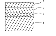
積層めっき被覆材
本発明による積層めっき被覆材(第1の態様)は、前記したように、非導電性基材の最表面に、ルテニウム(Ru)層またはルテニウム合金層が設けられた積層めっき被覆材であって、
非導電性基材と、ルテニウム層またはルテニウム合金層との間に、
下地層としての、ニッケル(Ni)層と、
その下地層の上に中間層としての、非貴金属層と
を有することを特徴とする。
Laminated Plating Coating Material The laminated plating coating material according to the present invention (the first embodiment) is, as described above, a laminated plating coating in which a ruthenium (Ru) layer or a ruthenium alloy layer is provided on the outermost surface of a nonconductive substrate. Materials,
Between the nonconductive substrate and the ruthenium layer or ruthenium alloy layer,
A nickel (Ni) layer as an underlayer;
A non-precious metal layer as an intermediate layer is provided on the underlayer.
ここで、積層めっき被覆材は、非導電性基材上に、下から、下地層、中間層、最表面層の三層構造からなる積層構造を有するものである。すなわち、本発明の積層めっき被覆材は、非導電性基材上に、下地層であるニッケル層、その下地層上に、中間層として非貴金属のめっき皮膜が形成され、その中間層上に、表面層であるRuまたはRu合金めっき皮膜が形成されてなる。
従って、本発明の積層めっき被覆材は、下地層であるニッケル層をニッケルめっきにより形成し、次いで、中間層である非貴金属層を、非貴金属めっきにより形成し、さらにその上に最表面層としてのルテニウム層またはルテニウム合金層を、ルテニウムめっきまたはルテニウム合金めっきにより形成することにより、得ることできる。
Here, the laminate plating coating material has a laminate structure comprising a three-layer structure of an underlayer, an intermediate layer, and an outermost layer from the bottom on a nonconductive substrate. That is, in the laminated plating coating material of the present invention, a non-precious metal plating film is formed as an intermediate layer on a non-conductive base material, a nickel layer which is an underlying layer, and an underlying layer. A surface layer of Ru or a Ru alloy plating film is formed.
Therefore, in the laminated plating coating material of the present invention, the nickel layer which is the underlayer is formed by nickel plating, then the non-precious metal layer which is the intermediate layer is formed by non-precious metal plating, and the outermost surface layer is further formed thereon. The ruthenium layer or the ruthenium alloy layer is formed by ruthenium plating or ruthenium alloy plating.
本発明における下地層、中間層および最表面層はいずれも、例えば、スパッタ法、蒸着法、湿式めっき法など慣用の方法を適宜用いて形成することができるが、作成の容易さや、被覆厚の制御の容易性などの観点から、湿式めっき法を用いてめっき被膜を形成することが好ましく、中でも電気めっき法を用いて形成することがより好ましい。 The underlayer, the intermediate layer and the outermost layer in the present invention can be formed as appropriate using, for example, a conventional method such as a sputtering method, a vapor deposition method, a wet plating method, etc. From the viewpoint of ease of control and the like, it is preferable to form a plating film using a wet plating method, and it is more preferable to form a plating film using an electroplating method among them.
従って、下地層であるニッケル層はニッケルめっき層と、中間層である非貴金属層は非貴金属めっき層と、さらに最表面層であるルテニウム層またはルテニウム合金層はそれぞれルテニウムめっき層またはルテニウム合金めっき層と言い換えることが出来る。 Therefore, the nickel layer which is the foundation layer is a nickel plating layer, the non-precious metal layer which is an intermediate layer is a non-precious metal plating layer, and the ruthenium layer or ruthenium alloy layer which is the outermost layer is a ruthenium plating layer or a ruthenium alloy plating layer, respectively. It can be paraphrased.
<ルテニウム層またはルテニウム合金層(最表面層)>
本発明の積層めっき被覆材の最表面層となるルテニウム層またはルテニウム合金層は、典型的には、電気めっき処理により形成させる。
<Ruthenium layer or ruthenium alloy layer (uppermost surface layer)>
The ruthenium layer or ruthenium alloy layer to be the outermost surface layer of the laminated plating coating material of the present invention is typically formed by electroplating.
本発明において、ルテニウムめっき処理に使用できるルテニウムめっき液は、本発明の非貴金属層の上にルテニウム層またはルテニウム合金層を形成できるものであれば、特に制限はない。典型的な例を挙げれば、ルテニウムめっき液には、ルテニウム化合物に加えて、電導性電解質など通常の白金族金属めっき液が含むことがある他の成分、界面活性剤、pH調整剤、緩衝剤、分散剤等の任意成分をさらに含んでいても良い。 In the present invention, the ruthenium plating solution that can be used for the ruthenium plating treatment is not particularly limited as long as it can form a ruthenium layer or a ruthenium alloy layer on the non-precious metal layer of the present invention. In a typical example, a ruthenium plating solution contains, in addition to a ruthenium compound, other components that a conventional platinum group metal plating solution such as a conductive electrolyte may contain, a surfactant, a pH adjuster, and a buffer. And optional components such as dispersants may be further included.
ここで使用可能なルテニウム化合物としては、水性であるめっき液に対して可溶性であって、かつ、めっき液中にルテニウムイオンを供給することができるものであれば特に制限はないが、例えば、硫酸ルテニウム、塩化ルテニウム、硝酸ルテニウム、スルファミン酸ルテニウムなどを好適例として挙げることができる。 The ruthenium compound that can be used here is not particularly limited as long as it is soluble in a plating solution that is aqueous and that can supply ruthenium ions into the plating solution, for example, sulfuric acid Ruthenium, ruthenium chloride, ruthenium nitrate, ruthenium sulfamate and the like can be mentioned as preferable examples.
ルテニウムめっき液において使用可能な電導性電解質としては、例えば、スルファミン酸塩、硝酸塩、塩化物、硫酸塩、しゅう酸塩、酒石酸塩、水酸化物、ホウ酸、ホウ酸塩、および炭酸塩からなる群より選択される1種以上のものが挙げられる。 Examples of the conductive electrolyte that can be used in the ruthenium plating solution include sulfamate, nitrate, chloride, sulfate, oxalate, tartrate, hydroxide, boric acid, borate, and carbonate. One or more kinds selected from the group are mentioned.
ルテニウムめっき液において、ルテニウム化合物の濃度は、例えば、ルテニウム量換算で1〜50g/Lに設定することができる。 In the ruthenium plating solution, the concentration of the ruthenium compound can be set to, for example, 1 to 50 g / L in terms of the amount of ruthenium.
最表面層がルテニウム合金層である場合には、ルテニウム合金めっき液を使用して、ルテニウム合金層を形成する。
ここで、ルテニウム合金めっきは、ルテニウムと、ニッケル、コバルト、金、銀、銅、鉄、亜鉛、スズ、白金、イリジウム、インジウム、鉄、パラジウムからなる群より選択される金属との合金めっきであるのがよい。好ましくはこのような金属は、パラジウムである。
When the outermost surface layer is a ruthenium alloy layer, a ruthenium alloy plating solution is used to form a ruthenium alloy layer.
Here, ruthenium alloy plating is alloy plating of ruthenium and a metal selected from the group consisting of nickel, cobalt, gold, silver, copper, iron, zinc, tin, platinum, iridium, indium, iron, and palladium. That's good. Preferably such metal is palladium.
本発明の好ましい態様では、ルテニウムめっき液またはルテニウム合金めっき液を使用して、めっき処理によりめっき被膜を形成してルテニウム層またはルテニウム合金層を形成するが、ここで行うめっき処理については、特に制限はなく、慣用のめっき処理方法および条件を必要に応じて適用することによって、めっき処理を実施ことができる。 In a preferred embodiment of the present invention, a ruthenium plating solution or a ruthenium alloy plating solution is used to form a plating film by plating to form a ruthenium layer or a ruthenium alloy layer, but the plating treatment performed here is particularly limited However, the plating process can be carried out by applying conventional plating methods and conditions as required.
例えば、めっき液のpHを1〜5の範囲内に調整する。まためっき液の温度は例えば30〜70℃の範囲内に調整し、めっき処理を行うことができる。
また、めっき処理における陰極電流密度は、例えば、0.2〜50A/dm2に設定することができる。形成されるめっき層の厚みは、必要であれば、適用される電流密度およびめっき時間等により適宜変更することができる。
For example, the pH of the plating solution is adjusted within the range of 1 to 5. Moreover, the temperature of a plating solution can be adjusted, for example in the range of 30-70 degreeC, and a plating process can be performed.
In addition, the cathode current density in the plating process can be set to, for example, 0.2 to 50 A / dm 2 . The thickness of the plating layer to be formed can be appropriately changed depending on the applied current density, plating time and the like, if necessary.
ルテニウム層またはルテニウム合金層の厚みは、特に限定されないが、通常は、0.01〜1μmの範囲であり、ルテニウムが高硬度でかつ高融点であるという特徴を利用して、より薄い範囲が好ましい範囲として上げることが出来る。従って、例えば、ルテニウム層またはルテニウム合金層の厚みは、0.5μm以下であることができ、好ましくは、0.1μmより薄くしておいてもよく、さらに好ましくは0.08μmより薄くしておいてもよい。前記したようにルテニウムには高硬度でかつ高融点であるという特徴があるため、本発明では、ロジウムなどの他の白金族金属の場合に比べて、機械的摩耗や発熱に対して強い特性を維持しつつ、より一層薄くすることができる。 The thickness of the ruthenium layer or ruthenium alloy layer is not particularly limited, but is usually in the range of 0.01 to 1 μm, and a thinner range is preferable, taking advantage of the high hardness and high melting point of ruthenium. It can be raised as a range. Thus, for example, the thickness of the ruthenium layer or ruthenium alloy layer may be 0.5 μm or less, preferably less than 0.1 μm, and more preferably less than 0.08 μm. It may be As described above, ruthenium is characterized by high hardness and high melting point, so the present invention is more resistant to mechanical abrasion and heat generation than other platinum group metals such as rhodium. It can be made thinner while maintaining it.
本発明においてはルテニウムを使用することを特徴としている。ルテニウムは、例えば硬くて高融点材料で知られているロジウムや、金などよりも、更に硬く高融点な金属であることから、本発明により、より耐熱性、耐食性に優れためっき皮膜を得ることが可能である。また、ルテニウムの貴金属価格は、金や、ロジウムを含む他の白金族金属に比べて安価であることから、本発明でのルテニウムの使用は、製品の低コスト化に有益である。 The present invention is characterized by using ruthenium. Ruthenium is a metal that is harder and has a high melting point than, for example, rhodium, which is known as a hard and high melting point material, and gold and the like, so that a plated film having better heat resistance and corrosion resistance is obtained by the present invention. Is possible. In addition, the use of ruthenium in the present invention is useful for reducing the cost of products, since the precious metal price of ruthenium is less expensive than gold and other platinum group metals including rhodium.
<非貴金属層(中間層)>
本発明の積層めっき被覆材において、非貴金属層は、下地層と最表面層との中間に位置し、非貴金属により構成され、典型的には、電気めっき処理により形成させる。
<Non-precious metal layer (intermediate layer)>
In the laminated plating coating material of the present invention, the non-precious metal layer is located between the underlayer and the outermost surface layer, is made of a non-precious metal, and is typically formed by electroplating.
ここで、非貴金属は、従来、Auめっきの代替えとして検討されていた白金族金属層の下層に使用し貴金属層で用いる貴金属とは異なるものであって、典型的には、Sn、Sn合金、またはNi合金からなる群より選択される。従って、本発明の積層めっき被覆材における中間層は、Sn、Sn合金、またはNi合金からなる層であることが好ましく、より好ましくは、Sn合金、Ni合金からなる層である。 Here, the non-precious metals are different from the precious metals used in the precious metal layer, which are conventionally used as the lower layer of the platinum group metal layer, which has been considered as an alternative to Au plating, and typically Sn, Sn alloy, Or selected from the group consisting of Ni alloys. Therefore, the intermediate layer in the laminate plating covering material of the present invention is preferably a layer composed of Sn, Sn alloy or Ni alloy, more preferably a layer composed of Sn alloy or Ni alloy.
一般的なルテニウムめっき液およびルテニウム合金めっき液は強酸性であるために、AlやCu系の基材に直接めっきを施すと基材そのものが侵され易い。本発明の中間層は、それを抑制するためにルテニウムめっき層の下に層を設けたものであるが、SnやNiなどの単金属の皮膜よりも、耐食性に優れる合金皮膜がより望ましい。 Since a general ruthenium plating solution and ruthenium alloy plating solution are strongly acidic, direct plating on an Al or Cu based substrate tends to corrode the substrate itself. The intermediate layer of the present invention is provided with a layer under the ruthenium plating layer in order to suppress it, but an alloy film having better corrosion resistance than a film of a single metal such as Sn or Ni is more desirable.
前記したSn合金としては、SnNi、SnCo、SnCu、SnPd、およびSnAgからなる群より選択されるものであることが好ましい。これらは耐食性に優れたものである。Sn合金としては、より好ましくは、SnNi、SnCu、SnPd、SnAgからなる群より選択されるものであり、さらに好ましくは、SnNiである。 The above-described Sn alloy is preferably selected from the group consisting of SnNi, SnCo, SnCu, SnPd, and SnAg. These are excellent in corrosion resistance. The Sn alloy is more preferably selected from the group consisting of SnNi, SnCu, SnPd, and SnAg, and still more preferably SnNi.
また前記したNi合金としては、NiW、またはNiWPであり、より好ましくは、NiWPである。 Moreover, as said Ni alloy, it is NiW or NiWP, More preferably, it is NiWP.
前記したSn合金およびNi合金で形成されうる合金被膜組成としては、例えば、下記の範囲のものが望ましいものとして挙げられる。
・SnNi合金: Sn 60〜75wt%(Ni25〜40wt%)
・SnCo合金: Sn 70〜85wt%(Co15〜30wt%)
・SnAg合金: Sn 96.5wt%(Ag3.5wt%)
・SnCu合金: Sn 35〜45wt%(Cu15〜30wt%)
・NiW合金: Ni 75〜55wt%(W25〜45wt%)
・NiWP合金: Ni 78.5〜60wt%(W20〜35wt%、P1.5〜5wt%)
As an alloy film composition which may be formed by the above-mentioned Sn alloy and Ni alloy, the thing of the following range is mentioned as a desirable thing, for example.
-SnNi alloy: 60 to 75 wt% of Sn (25 to 40 wt% of Ni)
-SnCo alloy: Sn 70-85 wt% (Co 15-30 wt%)
-SnAg alloy: Sn 96.5 wt% (Ag 3.5 wt%)
-SnCu alloy: Sn 35-45 wt% (Cu 15-30 wt%)
-NiW alloy: Ni 75-55 wt% (W 25-45 wt%)
-NiWP alloy: Ni 78.5-60 wt% (W 20-35 wt%, P 1.5-5 wt%)
本発明において、非貴金属層(中間層)の形成に使用できる非貴金属めっき液は、本発明の下地層(ニッケル層)の上に非貴金属層を形成できるものであれば、特に制限はない。典型的な例を挙げれば、めっき液には、スズ化合物、ニッケル化合物に加えて、電導性電解質などの他の成分、錯化剤、界面活性剤、pH調整剤、緩衝剤、分散剤等の任意成分をさらに含んでいても良い。 In the present invention, the non-noble metal plating solution that can be used to form the non-precious metal layer (intermediate layer) is not particularly limited as long as it can form the non-precious metal layer on the underlayer (nickel layer) of the present invention. Typical examples of the plating solution include, in addition to tin compounds and nickel compounds, other components such as conductive electrolytes, complexing agents, surfactants, pH adjusters, buffers, dispersing agents, etc. It may further contain an optional component.
ここで使用可能なスズ化合物および/またはニッケル化合物としては、水性であるめっき液に対して可溶性であって、かつ、めっき液中にスズイオンやニッケルイオンを供給することができる化合物や可溶性塩であれば特に制限はなく、スズやニッケルの例えば、塩化物、臭化物、ヨウ化物、硫化物、硝酸塩、亜硝酸塩、および亜硫酸塩を好適例として挙げることができる。 As the tin compound and / or nickel compound which can be used here, any compounds and soluble salts which are soluble in an aqueous plating solution and which can supply tin ions and nickel ions into the plating solution can be used. There is no particular limitation, and preferred examples include tin and nickel, for example, chloride, bromide, iodide, sulfide, nitrate, nitrite and sulfite.
非貴金属めっき液において使用可能な電導性電解質としては、例えば、スルファミン酸塩、硝酸塩、塩化物、硫酸塩、しゅう酸塩、酒石酸塩、水酸化物、ホウ酸、ホウ酸塩、および炭酸塩からなる群より選択される1種以上のものが挙げられる。 As conductive electrolytes that can be used in non-precious metal plating solutions, for example, from sulfamate, nitrate, chloride, sulfate, oxalate, tartrate, hydroxide, boric acid, borate and carbonate And at least one selected from the group consisting of
錯化剤としては、クエン酸、クエン酸塩、ピロリン酸、ピロリン酸塩、グルコン酸、グルコン酸塩、グリシンからなる群より選択される1種以上のものが挙げられる。 The complexing agent includes one or more selected from the group consisting of citric acid, citrate, pyrophosphate, pyrophosphate, gluconic acid, gluconate, and glycine.
本発明の好ましい態様では、非貴金属めっき液を使用して、めっき処理によりめっき被膜を形成して非貴金属層を形成するが、ここで行うめっき処理については、特に制限はなく、慣用のめっき処理方法および条件を必要に応じて適用することによって、めっき処理を実施ことができる。 In a preferred embodiment of the present invention, a non-precious metal plating solution is used to form a plating film by plating to form a non-precious metal layer, but the plating treatment performed here is not particularly limited, and conventional plating treatment The plating process can be performed by applying methods and conditions as needed.
例えば、めっき液のpHを1〜5の範囲内に調整する。まためっき液の温度は例えば30〜70℃の範囲内に調整し、めっき処理を行うことができる。
また、めっき処理における陰極電流密度は、例えば、0.2〜50A/dm2に設定することができる。形成されるめっき層の厚みは、必要であれば、適用される電流密度およびめっき時間等により適宜変更することができる。
For example, the pH of the plating solution is adjusted within the range of 1 to 5. Moreover, the temperature of a plating solution can be adjusted, for example in the range of 30-70 degreeC, and a plating process can be performed.
In addition, the cathode current density in the plating process can be set to, for example, 0.2 to 50 A / dm 2 . The thickness of the plating layer to be formed can be appropriately changed depending on the applied current density, plating time and the like, if necessary.
非貴金属層の厚みは、特に制限はされないが、通常は、0.05〜3μmの範囲であり、好ましくは、0.05〜1μmの範囲であり、より好ましくは、0.05〜0.8μmの範囲であり、さらに好ましくは、0.05〜0.5μmの範囲である。 The thickness of the non-precious metal layer is not particularly limited, but is usually in the range of 0.05 to 3 μm, preferably in the range of 0.05 to 1 μm, and more preferably 0.05 to 0.8 μm And more preferably in the range of 0.05 to 0.5 μm.
本発明では最表面層としてルテニウムまたはルテニウム合金による層を使用しており、ルテニウムは高融点、高沸点、高硬度な材料で、通常、緻密な被膜が得られることから、このことが、他の白金族金属を表面層として使用する場合に比べて、中間層をより薄くするに成功した一因と考えられる。ただし、前記説明は、考察の一例であり、本発明を拘束するものではない。 In the present invention, a layer of ruthenium or ruthenium alloy is used as the outermost surface layer, and ruthenium is a high melting point, high boiling point, high hardness material, and a dense film is usually obtained. This is considered to be one reason for the success in making the intermediate layer thinner compared to using platinum group metal as the surface layer. However, the above description is an example of consideration, and does not restrict the present invention.
<ニッケル層(下地層)>
本発明の積層めっき被覆材における下地層は、非導電性基体の上に形成される。好ましくは下地層は、導電処理された非導電性基材の上に形成される。本発明においては、下地層としては、基材成分の拡散を防止する事ができ、耐熱性を付与することのできるものとして、ニッケル層が使用される。
<Nickel layer (underlayer)>
The underlayer in the laminated plating coating material of the present invention is formed on a nonconductive substrate. Preferably, the underlayer is formed on a conductively treated nonconductive substrate. In the present invention, a nickel layer is used as the base layer as it can prevent the diffusion of the base component and can impart heat resistance.
本発明において、ニッケル層(下地層)の形成に使用できるニッケルめっき液は、本発明において非導電性基材の上に下地層を形成できるものであれば、特に制限はない。典型的な例を挙げれば、めっき液には、ニッケル化合物に加えて、電導性電解質などの他の成分、界面活性剤、pH調整剤、緩衝剤、分散剤等の任意成分をさらに含んでいても良い。 In the present invention, the nickel plating solution that can be used to form the nickel layer (base layer) is not particularly limited as long as the base layer can be formed on the nonconductive substrate in the present invention. Typically, in addition to the nickel compound, the plating solution further includes other components such as a conductive electrolyte, and optional components such as a surfactant, a pH adjuster, a buffer, and a dispersant. Also good.
ここで使用可能なニッケル化合物としては、水性であるめっき液に対して可溶性であって、かつ、めっき液中にニッケルイオンを供給することができる化合物や可溶性塩であれば特に制限はなく、ニッケルの例えば、塩化物、臭化物、ヨウ化物、硫化物、硝酸塩、亜硝酸塩、および亜硫酸塩を好適例として挙げることができる。 The nickel compound usable herein is not particularly limited as long as it is a compound or soluble salt that is soluble in a plating solution that is aqueous and that can supply nickel ions into the plating solution. For example, chlorides, bromides, iodides, sulfides, nitrates, nitrites and sulfites can be mentioned as preferred examples.
ニッケルめっき液において使用可能な電導性電解質としては、例えば、スルファミン酸塩、硝酸塩、塩化物、硫酸塩、しゅう酸塩、酒石酸塩、水酸化物、ホウ酸、ホウ酸塩、および炭酸塩からなる群より選択される1種以上のものが挙げられる。 Examples of conductive electrolytes that can be used in the nickel plating solution include sulfamate, nitrate, chloride, sulfate, oxalate, tartrate, hydroxide, boric acid, borate, and carbonate. One or more kinds selected from the group are mentioned.
本発明の好ましい態様では、ニッケルめっき液を使用して、めっき処理によりめっき被膜を形成してニッケル層を形成するが、ここで行うめっき処理については、特に制限はなく、慣用のめっき処理方法および条件を必要に応じて適用することによって、めっき処理を実施ことができる。 In a preferred embodiment of the present invention, a nickel plating solution is used to form a plating film by plating to form a nickel layer. There is no particular limitation on the plating performed here, and conventional plating methods and A plating process can be implemented by applying conditions as needed.
例えば、めっき液のpHを1〜5の範囲内に調整する。まためっき液の温度は例えば30〜70℃の範囲内に調整し、めっき処理を行うことができる。
また、めっき処理における陰極電流密度は、例えば、0.2〜50A/dm2に設定することができる。形成されるめっき層の厚みは、必要であれば、適用される電流密度およびめっき時間等により適宜変更することができる。
For example, the pH of the plating solution is adjusted within the range of 1 to 5. Moreover, the temperature of a plating solution can be adjusted, for example in the range of 30-70 degreeC, and a plating process can be performed.
In addition, the cathode current density in the plating process can be set to, for example, 0.2 to 50 A / dm 2 . The thickness of the plating layer to be formed can be appropriately changed depending on the applied current density, plating time and the like, if necessary.
ニッケル層の厚みは、特に制限はされないが、基体成分の拡散を防止でき、耐熱性を付与することのできる範囲であることが望ましく、通常は、1〜10μmの範囲であり、好ましくは、1〜8μmの範囲であり、より好ましくは、1〜5μmの範囲であり、さらに好ましくは、2〜5μmの範囲である。 The thickness of the nickel layer is not particularly limited, but is preferably in a range that can prevent the diffusion of the base component and can impart heat resistance, and is usually in the range of 1 to 10 μm, preferably 1 It is in the range of 8 μm, more preferably in the range of 1 to 5 μm, and still more preferably in the range of 2 to 5 μm.
<非導電性基材>
本発明に用いる非導電性基材は特に限定されるものではないが、例えば、樹脂材料またはセラミック材料などが挙げられる。具体的には、例えば、樹脂材料としては、ポリアクリルニトリル・ブタジエン・スチレン(ABS)やポリプロピレン(PP)、ポリフェニレンオキサイド(PPO)、ポリスルフォン(PS)、ポリカーボネート(PC)、ポリアセタール(PA)、ポリアミド(PA)などが挙げられる。また、セラミック材料としては、アルミナや安定化ジルコニア、炭化ケイ素、窒化ケイ素などが挙げられる。
<Non-conductive base material>
Although the non-electroconductive base material used for this invention is not specifically limited, For example, a resin material or a ceramic material etc. are mentioned. Specifically, for example, as a resin material, polyacrylonitrile butadiene styrene (ABS), polypropylene (PP), polyphenylene oxide (PPO), polysulfone (PS), polycarbonate (PC), polyacetal (PA), Polyamide (PA) etc. are mentioned. Further, as the ceramic material, alumina, stabilized zirconia, silicon carbide, silicon nitride and the like can be mentioned.
非導電性基材の厚さには特に制限はないが、例えば、0.05〜20mmであり、好ましくは、0.1〜5.0mmである。 Although there is no restriction | limiting in particular in the thickness of a nonelectroconductive base material, For example, it is 0.05-20 mm, Preferably, it is 0.1-5.0 mm.
本発明の好ましい態様によれば、非導電性基材は、下地層と接する表面が導電処理されてなる。すなわち、本発明において、非導電性基材における下地層と接する表面には、導電処理による導電処理面を有することが好ましい。非導電性基材の表面を導電処理することで、下地層を非導電性基材表面に形成し易くなる。ただし、下地層を非導電性基材表面上に形成する上で、非導電性基材表面を導電処理することなく形成することができるのであれば、必ずしも導電処理をする必要はない。 According to a preferred embodiment of the present invention, the non-conductive substrate has its surface in contact with the base layer subjected to a conductive treatment. That is, in the present invention, it is preferable that the surface of the nonconductive substrate in contact with the base layer have a conductive treatment surface by conductive treatment. The conductive treatment of the surface of the nonconductive substrate facilitates formation of the underlayer on the surface of the nonconductive substrate. However, when the base layer is formed on the surface of the nonconductive substrate, the surface of the nonconductive substrate can be formed without being subjected to the conductive treatment, so the conductive treatment is not necessarily required.
本発明において、非導電性基材表面に導電性を付与する導電処理を施す場合には、その処理方法は特に限定されるものではないが、その方法の例としては、例えば、スパッタ法、蒸着法、無電解めっき法、導電性塗料による塗装、導電性インクやペーストによる法、導電性金属箔の貼付などが挙げられる。 In the present invention, in the case where the surface of the non-conductive substrate is subjected to a conductive treatment for imparting conductivity, the treatment method is not particularly limited. Examples of the treatment method include sputtering, vapor deposition, and the like. The method includes an electroless plating method, coating with a conductive paint, a method with a conductive ink or paste, and application of a conductive metal foil.
前記導電処理により形成された導電処理面の材質としては、特に限定されるものではないが、例えば、銅、銅合金、ニッケル、ニッケル合金、アルミニウム、アルミニウム合金、ステンレス、ステンレス合金、パラジウム、コバルト、金等が挙げられる。 The material of the conductive treatment surface formed by the conductive treatment is not particularly limited, and, for example, copper, copper alloy, nickel, nickel alloy, aluminum, aluminum alloy, stainless steel, stainless steel alloy, palladium, cobalt, Money etc. can be mentioned.
導電処理方法として金属箔を貼付する方法による場合、使用する金属箔としては、例えば、市販の銅や銅合金箔、ニッケルやニッケル合金箔、アルミニウムやアルミニウム合金泊、ステンレスやステンレス合金箔、パラジウム箔や金箔などを用いることが出来る。 In the case of attaching a metal foil as the conductive processing method, for example, commercially available copper or copper alloy foil, nickel or nickel alloy foil, aluminum or aluminum alloy foil, stainless steel or stainless alloy foil, palladium foil Gold foil or the like can be used.
また、導電処理方法として無電解めっき法を使用する場合には、例えば、無電解銅めっき、無電解ニッケルめっき、無電解パラジウムめっき、無電解金めっき、無電解コバルトめっきなどを用いることができる。 Moreover, when using the electroless-plating method as a conductive processing method, electroless copper plating, electroless nickel plating, electroless palladium plating, electroless gold plating, electroless cobalt plating etc. can be used, for example.
導電処理方法として、無電解ニッケルめっきを使用する場合を例にさらに具体的に説明する。
ここで使用可能な無電解ニッケルめっき液は、本発明において非導電性基材の上に導電処理面を形成できるものであれば、特に制限はない。したがって、該めっき液には、導電処理面を形成できるのであれば、必要に応じて、ニッケル化合物に加えて、還元剤などの他の成分、錯化剤、pH調整剤、緩衝剤、安定剤等の任意成分をさらに含んでいても良い。
The case of using electroless nickel plating as the conductive processing method will be more specifically described by way of example.
The electroless nickel plating solution that can be used here is not particularly limited as long as it can form a conductive treated surface on the nonconductive substrate in the present invention. Therefore, in addition to the nickel compound, if necessary, the plating solution can form a conductive treated surface, and other components such as a reducing agent, a complexing agent, a pH adjusting agent, a buffer, and a stabilizer. And the like may further be included.
またここで使用可能なニッケル化合物としては、無電解ニッケルめっき浴に通常使用されるものを適宜用いることができる。ニッケル塩の具体例としては、硫酸ニッケル、塩化ニッケル、炭酸ニッケル、酢酸ニッケル、次亜リン酸ニッケル、スルファミン酸ニッケル、クエン酸ニッケルなどを挙げることができる。 Moreover, as a nickel compound which can be used here, what is normally used for an electroless nickel plating bath can be used suitably. Specific examples of the nickel salt include nickel sulfate, nickel chloride, nickel carbonate, nickel acetate, nickel hypophosphite, nickel sulfamate, nickel citrate and the like.
無電解ニッケルめっき液における還元剤としては、例えば次亜リン酸、次亜リン酸ナトリウム、亜リン酸ナトリウム、DMAB(ジメチルアミノボラン)、ヒドラジン一水和物、塩酸ヒドラジンや硫酸ヒドラジンなどのヒドラジン化合物が挙げられる。 As a reducing agent in the electroless nickel plating solution, for example, hypophosphorous acid, sodium hypophosphite, sodium phosphite, DMAB (dimethylaminoborane), hydrazine monohydrate, hydrazine compounds such as hydrazine hydrochloride or hydrazine sulfate Can be mentioned.
無電解ニッケルめっき液における錯化剤としては、乳酸、コハク酸、酒石酸、りんご酸、プロピオン酸、グリシン、グリコール酸、クエン酸、酢酸とそれらの塩などが挙げられる。 Examples of the complexing agent in the electroless nickel plating solution include lactic acid, succinic acid, tartaric acid, malic acid, propionic acid, glycine, glycolic acid, citric acid, acetic acid and salts thereof.
さらに、無電解ニッケルめっき浴には、上記以外にもpH緩衝剤や界面活性剤のような成分を含んでも良い。また、硫黄系安定剤や重金属安定剤を適宜含んでも良い。 In addition to the above, the electroless nickel plating bath may contain components such as a pH buffer and a surfactant. In addition, sulfur stabilizers and heavy metal stabilizers may be appropriately contained.
無電解ニッケルによる導電処理面の厚みは、特に制限はされないが、通常は、0.1〜10μmの範囲であり、好ましくは、0.5〜8μmの範囲であり、より好ましくは、1〜5μmの範囲であり、さらに好ましくは、1〜3μmの範囲である。 Although the thickness of the conductive treatment surface by electroless nickel is not particularly limited, it is usually in the range of 0.1 to 10 μm, preferably in the range of 0.5 to 8 μm, more preferably 1 to 5 μm. And more preferably in the range of 1 to 3 μm.
導電処理面に無電解ニッケルなどを用いた場合には、必ずしも下地層(ニッケル層)は必要なく、省略することも可能である。したがって、本発明の別の好ましい態様によれば、前記した本発明の積層めっき被覆材(第1の態様)において、下地層の代わりに、非導電性基材の表面が導電処理されて形成された導電処理面を有する、積層めっき被覆材が提供できる。 When electroless nickel or the like is used for the conductive treatment surface, the underlayer (nickel layer) is not necessarily required, and may be omitted. Therefore, according to another preferred embodiment of the present invention, in the above-described laminated plating covering material (first embodiment) of the present invention, the surface of the non-conductive substrate is conductively formed instead of the underlayer. It is possible to provide a laminated plating coating material having a conductive treated surface.
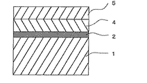
すなわち、本発明の別の態様として、下記の積層めっき被覆材(本発明の第2の態様)が提供できる:
非導電性基材の最表面に、ルテニウム(Ru)層またはルテニウム合金層が設けられた積層めっき被覆材であって、
非導電性基材と、ルテニウム層またはルテニウム合金層との間に、
中間層としての、非貴金属層
を有し、かつ
非導電性基材が中間層と接する表面が導電処理されてなる、積層めっき被覆材。
That is, as another aspect of the present invention, the following laminate plating covering material (second aspect of the present invention) can be provided:
It is a laminated plating covering material in which a ruthenium (Ru) layer or a ruthenium alloy layer is provided on the outermost surface of a nonconductive substrate,
Between the nonconductive substrate and the ruthenium layer or ruthenium alloy layer,
A laminated plating coating material having a non-precious metal layer as an intermediate layer, and a surface of a nonconductive substrate in contact with the intermediate layer being subjected to a conductive treatment.
すなわち、この本発明の別の態様は、非導電性基材と、下地層と、中間層と、ルテニウム(Ru)層またはルテニウム合金層とを有する本発明の積層めっき被覆材において、下地層の代わりに、導電処理面を有するものであるといえる。この本発明の別の態様は、下地層の代わりに導電処理面を有すること以外は、上記した非導電性基材と、下地層と、中間層と、ルテニウム(Ru)層またはルテニウム合金層とを有する本発明の積層めっき被覆材と同様の構成をとることができる。 That is, another aspect of the present invention is a laminate plating covering material of the present invention comprising a nonconductive substrate, an underlayer, an intermediate layer, and a ruthenium (Ru) layer or a ruthenium alloy layer, wherein Instead, it can be said to have a conductive treatment surface. Another aspect of the present invention is that the nonconductive substrate described above, the underlayer, the intermediate layer, the ruthenium (Ru) layer, or the ruthenium alloy layer, except that it has a conductive treated surface instead of the underlayer. The same constitution as the laminated plating coating material of the present invention having the
積層めっき被覆材の製造方法
本発明による積層めっき被覆材の製造方法は、前記したように、
非導電性基材の表面上に、
Niめっきにより、下地層を形成させ、
下地層の上に、非貴金属めっきにより、中間層を形成させ、
中間層の上に、ルテニウムめっきまたはルテニウム合金めっきにより、最表面層を形成させる工程を含む。好ましくは、前記方法において、非導電性基材の表面が導電処理した後、下地層を形成させることを含む。
Method for Producing Laminated Plating Coating Material As described above, the method for producing a laminated plating coating material according to the present invention
On the surface of the nonconductive substrate,
A base layer is formed by Ni plating,
An intermediate layer is formed on the underlayer by non-precious metal plating,
A step of forming an outermost layer by ruthenium plating or ruthenium alloy plating on the intermediate layer is included. Preferably, the method includes forming an underlayer after the surface of the non-conductive substrate has been subjected to a conductive treatment.
本発明の別の態様によれば、前記した本発明の方法において、下地層を形成させる代わりに、非導電性基材の表面を導電処理して導電処理面を形成させることができる。これにより前述した本発明の第2の態様の被覆材を製造することができる。 According to another aspect of the present invention, in the above-described method of the present invention, instead of forming the underlayer, the surface of the nonconductive substrate can be subjected to a conductive treatment to form a conductive treated surface. Thereby, the coating material of the second aspect of the present invention described above can be manufactured.
本発明による方法の典型的な工程は、例えば、基材が非導電性の樹脂材料である場合には、まず、脱脂処理を非導電性基材の表面に施し、エッチング処理、酸洗処理を行い、
ついで、触媒付与処理と無電解Niを施し、電解脱脂処理を施した上で、酸洗浄を行い、その上で、上記のように、Niめっきにより下地層を形成させ、次いで、下地層の上に、非貴金属めっきにより中間層を形成させ、さらに、中間層の上に、ルテニウムめっきまたはルテニウム合金めっきにより、最表面層を形成させる。
Typical steps of the method according to the present invention, for example, when the substrate is a nonconductive resin material, first, a degreasing treatment is applied to the surface of the nonconductive substrate, and an etching treatment and an acid pickling treatment are carried out. Do,
Next, a catalyst application treatment and electroless Ni are applied, electrolytic degreasing is applied, acid cleaning is performed, and an undercoat layer is formed by Ni plating as described above, and then, on the undercoat layer Then, the intermediate layer is formed by non-precious metal plating, and the outermost surface layer is formed by ruthenium plating or ruthenium alloy plating on the intermediate layer.
本発明におけるルテニウム層またはルテニウム合金層(最表面層)は、(必要に応じて導電処理した)非導電性基材上の少なくともルテニウム皮膜の特性を必要とする部分(例えば、耐食性、低接触抵抗性の確保などを目的として使用される箇所)の表面に形成されていればよく、ルテニウム皮膜の特性を必ずしも必要としない他の部分においては、ルテニウム層またはルテニウム合金層を設ける必要はない。このため、例えば、電気めっき法であれば、片面のみのめっきや、ストライプめっき、スポットめっきなどの部分めっきで形成されていても良い。 The ruthenium layer or ruthenium alloy layer (uppermost surface layer) in the present invention is a portion (for example, corrosion resistance, low contact resistance) which requires at least the characteristics of a ruthenium film on a nonconductive substrate (electrically treated if necessary) As long as it is formed on the surface of a portion used for the purpose of securing the property etc., it is not necessary to provide a ruthenium layer or a ruthenium alloy layer in other portions which do not necessarily require the properties of the ruthenium film. Therefore, for example, in the case of electroplating, it may be formed by partial plating such as plating on only one side, stripe plating, spot plating, or the like.
本発明による積層めっき被覆材は、導電性であって、耐食性に優れ、接触抵抗が低いことから、コネクタ、摺動接点、タクトスイッチ、シートスイッチ、摺動接点などの電気的接続を必要とする電気接点に適用することができ、また、基材成分の拡散を抑制できるため、例えば、LED、燃料電池用電極、燃料電池用集電板、プリント配線板などに適用することができ、さらに、さらに、より耐食性が求められる自動車向け半導体やパワー半導体などにも適用することが出来る。 The laminated plating coating material according to the present invention is electrically conductive, has excellent corrosion resistance and low contact resistance, and thus requires electrical connection such as a connector, sliding contact, tact switch, sheet switch, sliding contact, etc. The present invention can be applied to electrical contacts and can suppress the diffusion of base components, and can be applied to, for example, LEDs, electrodes for fuel cells, current collectors for fuel cells, printed wiring boards, etc. Furthermore, the present invention can be applied to automotive semiconductors and power semiconductors that are required to have higher corrosion resistance.
以下において、本発明を下記の実施例によって詳細に説明するが、本発明はこれらに限定されるものではない。 The present invention will be described in detail by the following examples, but the present invention is not limited thereto.
以下に示す[1]〜[3]の試験を行った。 The following tests [1] to [3] were performed.
[1] 試験用皮膜の作成と外観の観察
(試験片1〜9の作成)
20mm×25mmのCu板に、図4に示した試験片1および試験片2に示す皮膜構成の試験片を作成した。試験片2は、試験片1におけるSnNiめっき層をNiWめっき層にしたものであり、試験片1と同様の手順にて作成した。
また、下地層にAuめっき処理を施した試験片を、試験片3として作製した。
[1] Preparation of test film and observation of appearance
(Preparation of
The test piece of the film | membrane structure shown to the
In addition, a test piece in which the underlayer was subjected to Au plating was manufactured as a
具体的には、Cu板へのめっき皮膜の作成は、図6に示した手順に従って行った。なお、手順の各工程の間では、水洗処理を行った。 Specifically, the formation of the plated film on the Cu plate was performed according to the procedure shown in FIG. In addition, the water washing process was performed between each process of a procedure.
20mm×25mmの樹脂(ABS(ポリアクリルニトリル・ブタジエン・スチレン))板に、図4および図5に示した試験片4および試験片5に示す皮膜構成の試験片を作成した。試験片5は、試験片4におけるSnNiめっき層をNiWめっき層にしたものであり、試験片2と同様の手順にて作製した。
On the 20 mm × 25 mm resin (ABS (polyacrylonitrile butadiene styrene)) plate, test pieces of the film configuration shown in the
試験片6および試験片7は、試験片4および試験片5の皮膜構成から「下地層」(ニッケル層)を省略したものであり、それ以外は試験片4および試験片5と同様の手順にて作製した。
The test pieces 6 and 7 are obtained by omitting the “underlayer” (nickel layer) from the film configuration of the
具体的には、ABS板へのめっき皮膜の作成は、図6および図7に示した手順に従って行った。なお、手順の各工程の間では、水洗処理を行った。 Specifically, the formation of the plating film on the ABS plate was performed according to the procedure shown in FIG. 6 and FIG. In addition, the water washing process was performed between each process of a procedure.
銅箔が貼られた20mm×25mmのABS板に、図5に示した試験片8および試験片9に示す皮膜構成の試験片を作成した。試験片9は、試験片8におけるSnNiめっき層をNiWめっき層にしたものであり、試験片8と同様の手順にて作製した。 The test piece of the film | membrane structure shown to the test piece 8 shown in FIG. 5 and the test piece 9 was created on the 20 mm x 25 mm ABS board to which copper foil was stuck. The test piece 9 was obtained by forming the SnNi plated layer on the test piece 8 into a NiW plated layer, and was produced in the same procedure as the test piece 8.
試験片8および試験片9の作成手順は、図7に示したよう試験片1及び試験片2と同様の手順にて作製した。
The preparation procedure of the test piece 8 and the test piece 9 was produced in the procedure similar to the
ここで、各めっき条件と浴組成は、下記の表1の通りとした。 Here, each plating condition and bath composition were as Table 1 below.
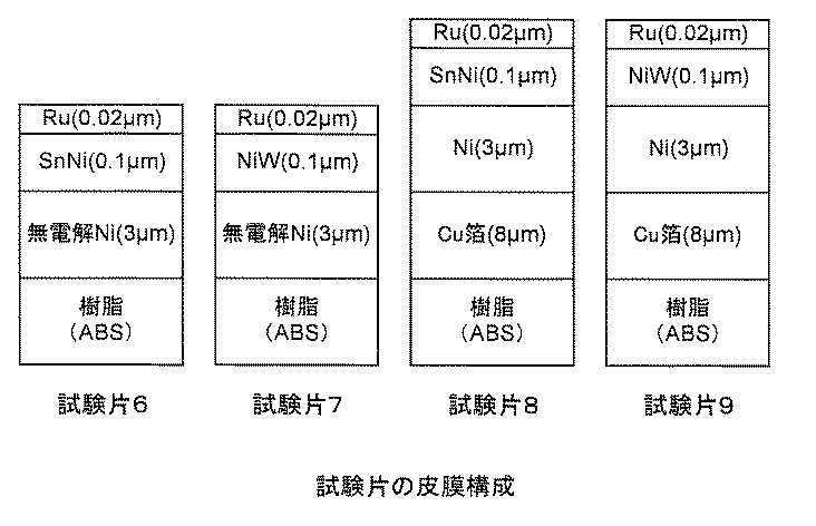
各めっき処理は、各めっき厚がそれぞれ下記の膜厚になるように行った。
無電解Ni:3μm
Ni: 3μm
SnNi: 0.1μm
Ru: 0.02μm
NiW: 0.1μm
Au: 0.02μm
Each plating process was performed so that each plating thickness became the following film thickness, respectively.
Electroless Ni: 3 μm
Ni: 3 μm
SnNi: 0.1 μm
Ru: 0.02 μm
NiW: 0.1 μm
Au: 0.02 μm
以上のようにして、試験片1(参考例)、試験片2(参考例)、および試験片3(比較例)、試験片4(本発明)、試験片5(本発明)、試験片6(本発明)、試験片7(本発明)を得た。 As described above, test strip 1 (reference example), test strip 2 (reference example), test strip 3 (comparative example), test strip 4 (invention), test strip 5 (invention), test strip 6 (Invention) Test specimen 7 (invention) was obtained.
(試験片1〜9の外観観察)
作成された試験片1〜9の外観を目視で観察した。
(Appearance observation of
The appearance of the produced
Ru/Niのみからなる層の場合には、通常、良質なRu被膜外観を得るのは難しいところ、試験片1〜9はいずれも、クラックやピンホールの無い良質なRu皮膜外観を有するものであった。
In the case of a layer consisting only of Ru / Ni, it is usually difficult to obtain a good Ru coating appearance, but all the
従って、試験片1および試験片2は、Auめっきを用いる従来の方法によるもの(試験片3)と同等の皮膜外観を得ることができたことから、Auめっきを削減でき低コスト化が可能であることが確認できた。
Therefore, since the
非導電性の樹脂基材を用いた試験片4、試験片5、試験片6及び試験片7は、導電性金属基材を用いる従来の方法によるもの(試験片1,試験片2,試験片3)と同等の皮膜外観を得ることができたことから、本発明により、軽量化、低コスト化が可能であることが確認できた。
The
[2] 耐食性試験(硝酸ばっ気試験)
前記[1]にて作成した試験片1、試験片2、および試験片4〜9について、JIS−H8620附属書1に従って、硝酸ばっ気試験を行った。
[2] Corrosion resistance test (nitric acid aeration test)
The nitric acid aeration test was performed according to JIS-
まず、各試験片の汚れをエタノールで除去して乾燥させた後、容積2Lのデシケーターの底部に5mlの硝酸を入れ、磁製板の上に試験片を載せて蓋をして、約23℃で1時間放置した。 First, after removing the stains of each test piece with ethanol and drying, add 5 ml of nitric acid to the bottom of a 2 L desiccator, place the test piece on a porcelain plate, cover it, and approximately 23 ° C. Left for 1 hour.
次いで、試験片を取り出し、静かに水洗して乾燥させた後、試験片の表面の皮膜を、デジタルマイクロスコープにて観察し、以下の基準にて評価した。 Next, the test piece was taken out, gently washed with water and dried, and the film on the surface of the test piece was observed with a digital microscope and evaluated according to the following criteria.
<評価基準>
A:めっき皮膜に、膨れや剥がれが無い。
B:めっき皮膜に、僅かな膨れや剥がれを有する。
C:めっき皮膜に、著しい膨れや剥がれを有する。
<Evaluation criteria>
A: There is no swelling or peeling on the plating film.
B: The plating film has slight swelling and peeling.
C: The plating film has significant swelling and peeling.
<評価結果>
評価の結果は下記の表のとおりであった。
<Evaluation result>
The results of the evaluation were as shown in the following table.
したがって、試験片1および試験片2と同様に、試験片4〜9のいずれについても、硝酸ばっ気試験後であっても、膨れや剥がれ等の無い良質な皮膜となったことが確認できた。
Therefore, as in the case of the
[3] 接触抵抗測定試験
前記[1]にて作成した試験片1、試験片2、および試験片4〜9について、電気接点シミュレーター(株式会社山崎精機研究所製、CRS−113−AU型)を用いて、試験片作成直後において、接触抵抗を測定した。
[3] Contact resistance measurement test For the
また、試験片の作成直後に加えて、各試験片を、高温高湿試験機に入れて、150℃、85%RHの環境下において352時間保持した後に、各試験片の接触抵抗の測定も行った。 In addition, immediately after the preparation of the test pieces, each test piece is placed in a high-temperature high-humidity tester and held for 352 hours in an environment of 150 ° C., 85% RH, and then the contact resistance of each test piece is also measured. went.
測定条件は、印加電流10mA、解放電圧20mA以下、荷重0.05N、走査速度1mm/minとし、4端子法にて測定を行った。 The measurement conditions were an applied current of 10 mA, a release voltage of 20 mA or less, a load of 0.05 N, and a scanning speed of 1 mm / min.
結果は下記のとおりであった。 The results were as follows.
試験片1:
試験片作製直後の接触抵抗7.23mΩに対し、150℃、85%RHの環境下で352時間保持後の接触抵抗は10.26mΩとなり、抵抗値の上昇を142%程度に抑制することが出来た。
Test piece 1:
The contact resistance after holding for 352 hours in an environment of 150 ° C. and 85% RH is 10.26 mΩ against the contact resistance of 7.23 mΩ immediately after the preparation of the test piece, and the increase in resistance value can be suppressed to about 142%. The
試験片2:
試験片作製直後の接触抵抗7.62mΩに対し、150℃、85%RHの環境下で352時間保持後の接触抵抗は11.53mΩとなり、抵抗値の上昇を151%程度に抑制することが出来た。
Specimen 2:
The contact resistance after holding for 352 hours under the environment of 150 ° C. and 85% RH is 11.53 mΩ against the contact resistance of 7.62 mΩ immediately after the preparation of the test piece, and the increase of the resistance value can be suppressed to about 151%. The
試験片4:
試験片作製直後の接触抵抗7.37mΩに対し、150℃、85%RHの環境下で352時間保持後の接触抵抗は10.91mΩとなり、抵抗値の上昇を148%程度に抑制することが出来た。
Test specimen 4:
The contact resistance after holding for 352 hours in an environment of 150 ° C. and 85% RH is 10.91 mΩ against the contact resistance of 7.37 mΩ immediately after preparation of the test piece, and the rise in resistance value can be suppressed to about 148%. The
試験片5:
試験片作製直後の接触抵抗7.55mΩに対し、150℃、85%RHの環境下で352時間保持後の接触抵抗は11.87mΩとなり、抵抗値の上昇を157%程度に抑制することが出来た。
Specimen 5:
The contact resistance after holding for 352 hours in an environment of 150 ° C. and 85% RH is 11.87 mΩ against the contact resistance of 7.55 mΩ immediately after the preparation of the test piece, and the increase in resistance value can be suppressed to about 157%. The
試験片6:
試験片作製直後の接触抵抗7.51mΩに対し、150℃、85%RHの環境下で352時間保持後の接触抵抗は11.11mΩとなり、抵抗値の上昇を148%程度に抑制することが出来た。
Specimen 6:
The contact resistance after holding for 352 hours in an environment of 150 ° C. and 85% RH is 11.11 mΩ against the contact resistance of 7.51 mΩ immediately after the preparation of the test piece, and the increase of the resistance value can be suppressed to about 148%. The
試験片7:
試験片作製直後の接触抵抗7.72mΩに対し、150℃、85%RHの環境下で352時間保持後の接触抵抗は12.02mΩとなり、抵抗値の上昇を156%程度に抑制することが出来た。
Test specimen 7:
The contact resistance after holding for 352 hours under the environment of 150 ° C. and 85% RH is 12.02 mΩ against the contact resistance of 7.72 mΩ immediately after the preparation of the test piece, and the increase of the resistance value can be suppressed to about 156%. The
試験片8:
試験片作製直後の接触抵抗7.03mΩに対し、150℃、85%RHの環境下で352時間保持後の接触抵抗は10.32mΩとなり、抵抗値の上昇を147%程度に抑制することが出来た。
Specimen 8:
The contact resistance after holding for 352 hours in an environment of 150 ° C. and 85% RH is 10.32 mΩ against the contact resistance of 7.03 mΩ immediately after preparation of the test piece, and the increase in resistance value can be suppressed to about 147%. The
試験片9:
試験片作製直後の接触抵抗7.06mΩに対し、150℃、85%RHの環境下で352時間保持後の接触抵抗は11.63mΩとなり、抵抗値の上昇を165%程度に抑制することが出来た。
Specimen 9:
The contact resistance after holding for 352 hours under the environment of 150 ° C. and 85% RH is 11.63 mΩ against the contact resistance of 7.06 mΩ immediately after the preparation of the test piece, and the increase of the resistance value can be suppressed to about 165%. The
以上の[1]〜[3]の試験結果から、本発明によれば、非導電性基材に対し、高価なAuを用いること無く、低コストで耐食性に優れ、且つ接触抵抗劣化の少ない、金属基材を用いたものよりも軽量なめっき被覆材を得ることができることが確認できた。 From the above test results of [1] to [3], according to the present invention, the non-conductive substrate does not use expensive Au, is low in cost, excellent in corrosion resistance, and is less in contact resistance deterioration. It has been confirmed that a plated coating material lighter than that using a metal substrate can be obtained.
1 非導電性基材
2 導電処理面
3 下地層
4 中間層
5 最表面層
1
Claims (9)
非導電性基材と、ルテニウム層またはルテニウム合金層との間に、
下地層としての、ニッケル(Ni)層と、
その上に中間層としての、非貴金属層と
を有することを特徴とする、積層めっき被覆材。 It is a laminated plating covering material in which a ruthenium (Ru) layer or a ruthenium alloy layer is provided on the outermost surface of a nonconductive substrate,
Between the nonconductive substrate and the ruthenium layer or ruthenium alloy layer,
A nickel (Ni) layer as an underlayer;
What is claimed is: 1. A laminate plating covering material comprising: a non-precious metal layer as an intermediate layer thereon.
Ni合金が、NiW、またはNiWPである、請求項5に記載の積層めっき被覆材。 The laminate plating covering material according to claim 5, wherein the Sn alloy is SnNi, SnCo, SnCu, SnPd, or SnAg, and the Ni alloy is NiW or NiWP.
Niめっきにより、下地層を形成させ、
下地層の上に、非貴金属めっきにより、中間層を形成させ、
中間層の上に、ルテニウムめっきまたはルテニウム合金めっきにより、最表面層を形成させる
工程を含む、積層めっき被覆材の製造方法。 On the surface of the nonconductive substrate,
A base layer is formed by Ni plating,
An intermediate layer is formed on the underlayer by non-precious metal plating,
A method for producing a laminated plating covering material, comprising the step of forming an outermost surface layer by ruthenium plating or ruthenium alloy plating on an intermediate layer.
The method according to claim 7, wherein the surface of the non-conductive substrate is subjected to a conductive treatment to form a conductive treated surface, instead of forming the underlayer.
Priority Applications (1)
| Application Number | Priority Date | Filing Date | Title |
|---|---|---|---|
| JP2017084770A JP6649915B2 (en) | 2017-04-21 | 2017-04-21 | Ruthenium-containing laminated plating coating material |
Applications Claiming Priority (1)
| Application Number | Priority Date | Filing Date | Title |
|---|---|---|---|
| JP2017084770A JP6649915B2 (en) | 2017-04-21 | 2017-04-21 | Ruthenium-containing laminated plating coating material |
Publications (3)
| Publication Number | Publication Date |
|---|---|
| JP2018178237A true JP2018178237A (en) | 2018-11-15 |
| JP2018178237A5 JP2018178237A5 (en) | 2020-01-23 |
| JP6649915B2 JP6649915B2 (en) | 2020-02-19 |
Family
ID=64282945
Family Applications (1)
| Application Number | Title | Priority Date | Filing Date |
|---|---|---|---|
| JP2017084770A Active JP6649915B2 (en) | 2017-04-21 | 2017-04-21 | Ruthenium-containing laminated plating coating material |
Country Status (1)
| Country | Link |
|---|---|
| JP (1) | JP6649915B2 (en) |
Cited By (1)
| Publication number | Priority date | Publication date | Assignee | Title |
|---|---|---|---|---|
| KR102075469B1 (en) | 2019-06-21 | 2020-02-10 | 사이먼앤코(주) | Connector and Manufacturing Method of it |
Citations (14)
| Publication number | Priority date | Publication date | Assignee | Title |
|---|---|---|---|---|
| JPS628533A (en) * | 1985-07-05 | 1987-01-16 | Hitachi Ltd | Gold-plated electronic component package |
| JPH06228788A (en) * | 1993-01-29 | 1994-08-16 | Pentel Kk | Production of noble metal plating |
| JPH0711478A (en) * | 1993-06-29 | 1995-01-13 | Pentel Kk | Production of noble metal plated material |
| JPH10233121A (en) * | 1997-02-18 | 1998-09-02 | Hitachi Cable Ltd | Lead wire |
| JP2001155740A (en) * | 1999-11-25 | 2001-06-08 | Matsushita Electric Works Ltd | Electrode for fuel cell |
| JP2002241986A (en) * | 2001-02-20 | 2002-08-28 | Osaka Prefecture | Ni-W-P ALLOY PLATING SOLUTION AND CONTINUOUS PLATING METHOD THEREWITH |
| US20030003292A1 (en) * | 2000-11-24 | 2003-01-02 | Masakazu Anpo | Composite element and method for preparation thereof |
| JP2003003292A (en) * | 2001-05-11 | 2003-01-08 | Lucent Technol Inc | Coated metallic product |
| US20090202862A1 (en) * | 2006-06-26 | 2009-08-13 | Liang Chen | Electroplated device and preparation method thereof |
| JP2009215632A (en) * | 2008-03-12 | 2009-09-24 | Furukawa Electric Co Ltd:The | Metallic material for electric contact component |
| JP2015045058A (en) * | 2013-08-27 | 2015-03-12 | Jx日鉱日石金属株式会社 | Metallic material for electronic component and manufacturing method of the same, and connector terminal, connector, and electronic component using the same |
| CN105018908A (en) * | 2015-03-23 | 2015-11-04 | 深圳市贝加电子材料有限公司 | Chemical ruthenium plating solution for circuit board surface treatment and circuit board surface treatment method |
| CN106048680A (en) * | 2016-07-22 | 2016-10-26 | 东莞普瑞得五金塑胶制品有限公司 | Special galvanical corrosion-resistant coating for fast charging interface of mobile phone |
| US20170084392A1 (en) * | 2015-09-17 | 2017-03-23 | Samsung Electro-Mechanics Co., Ltd. | Multilayer ceramic capacitor |
-
2017
- 2017-04-21 JP JP2017084770A patent/JP6649915B2/en active Active
Patent Citations (14)
| Publication number | Priority date | Publication date | Assignee | Title |
|---|---|---|---|---|
| JPS628533A (en) * | 1985-07-05 | 1987-01-16 | Hitachi Ltd | Gold-plated electronic component package |
| JPH06228788A (en) * | 1993-01-29 | 1994-08-16 | Pentel Kk | Production of noble metal plating |
| JPH0711478A (en) * | 1993-06-29 | 1995-01-13 | Pentel Kk | Production of noble metal plated material |
| JPH10233121A (en) * | 1997-02-18 | 1998-09-02 | Hitachi Cable Ltd | Lead wire |
| JP2001155740A (en) * | 1999-11-25 | 2001-06-08 | Matsushita Electric Works Ltd | Electrode for fuel cell |
| US20030003292A1 (en) * | 2000-11-24 | 2003-01-02 | Masakazu Anpo | Composite element and method for preparation thereof |
| JP2002241986A (en) * | 2001-02-20 | 2002-08-28 | Osaka Prefecture | Ni-W-P ALLOY PLATING SOLUTION AND CONTINUOUS PLATING METHOD THEREWITH |
| JP2003003292A (en) * | 2001-05-11 | 2003-01-08 | Lucent Technol Inc | Coated metallic product |
| US20090202862A1 (en) * | 2006-06-26 | 2009-08-13 | Liang Chen | Electroplated device and preparation method thereof |
| JP2009215632A (en) * | 2008-03-12 | 2009-09-24 | Furukawa Electric Co Ltd:The | Metallic material for electric contact component |
| JP2015045058A (en) * | 2013-08-27 | 2015-03-12 | Jx日鉱日石金属株式会社 | Metallic material for electronic component and manufacturing method of the same, and connector terminal, connector, and electronic component using the same |
| CN105018908A (en) * | 2015-03-23 | 2015-11-04 | 深圳市贝加电子材料有限公司 | Chemical ruthenium plating solution for circuit board surface treatment and circuit board surface treatment method |
| US20170084392A1 (en) * | 2015-09-17 | 2017-03-23 | Samsung Electro-Mechanics Co., Ltd. | Multilayer ceramic capacitor |
| CN106048680A (en) * | 2016-07-22 | 2016-10-26 | 东莞普瑞得五金塑胶制品有限公司 | Special galvanical corrosion-resistant coating for fast charging interface of mobile phone |
Cited By (1)
| Publication number | Priority date | Publication date | Assignee | Title |
|---|---|---|---|---|
| KR102075469B1 (en) | 2019-06-21 | 2020-02-10 | 사이먼앤코(주) | Connector and Manufacturing Method of it |
Also Published As
| Publication number | Publication date |
|---|---|
| JP6649915B2 (en) | 2020-02-19 |
Similar Documents
| Publication | Publication Date | Title |
|---|---|---|
| JP6495172B2 (en) | Metal plating coated stainless steel and method for producing metal plating coated stainless steel | |
| TW211588B (en) | ||
| TW200842212A (en) | Silver-coated material for movable contact parts and method of producing the same | |
| JP6231982B2 (en) | Electroless gold plating method and gold plating coating material | |
| EP3467152A1 (en) | Surface treatment material, production method thereof, and component formed using surface treatment material | |
| US20140076618A1 (en) | Method of forming gold thin film and printed circuit board | |
| JP2013105629A (en) | Current collector plate for fuel cell and method for manufacturing the same | |
| JP6450300B2 (en) | Laminated plating coating material containing ruthenium and method for producing the same | |
| JP6649915B2 (en) | Ruthenium-containing laminated plating coating material | |
| JP6193687B2 (en) | Silver plating material and method for producing the same | |
| JP6587848B2 (en) | Fuel cell energization member, fuel cell, fuel cell stack, and fuel cell energization member manufacturing method | |
| JP6254942B2 (en) | FUEL CELL SEPARATOR, FUEL CELL CELL, FUEL CELL STACK, AND METHOD FOR MANUFACTURING FUEL CELL SEPARATOR | |
| JP6199086B2 (en) | Palladium-plated coating material and method for producing palladium-plated coating material | |
| JP2018193578A (en) | Tin-plated copper terminal material, and end part structure of electric wire | |
| JP4847179B2 (en) | Titanium or titanium alloy material with precious metal plating | |
| JP7068899B2 (en) | Rhodium phosphorus plating film and laminate material | |
| JP6754152B1 (en) | Plating laminate | |
| JP2022057398A (en) | Plated product | |
| JP5879093B2 (en) | Connector manufacturing method and silver plating method | |
| JP2023056185A (en) | PtRu ALLOY PLATING FILM, AND LAMINATED STRUCTURE OF PtRu ALLOY PLATING FILMS | |
| TW202348407A (en) | Laminated structure with ptru alloy thin film | |
| JP2005194561A (en) | Plating method, and method for manufacturing electronic component | |
| WO2014208610A1 (en) | Conductive member | |
| JP2020145071A (en) | Electrical contact terminal | |
| JP2009084590A (en) | Method for producing metal plated stainless steel sheet material |
Legal Events
| Date | Code | Title | Description |
|---|---|---|---|
| A621 | Written request for application examination |
Free format text: JAPANESE INTERMEDIATE CODE: A621 Effective date: 20191030 |
|
| A521 | Request for written amendment filed |
Free format text: JAPANESE INTERMEDIATE CODE: A523 Effective date: 20191205 |
|
| A871 | Explanation of circumstances concerning accelerated examination |
Free format text: JAPANESE INTERMEDIATE CODE: A871 Effective date: 20191205 |
|
| A975 | Report on accelerated examination |
Free format text: JAPANESE INTERMEDIATE CODE: A971005 Effective date: 20191212 |
|
| TRDD | Decision of grant or rejection written | ||
| A01 | Written decision to grant a patent or to grant a registration (utility model) |
Free format text: JAPANESE INTERMEDIATE CODE: A01 Effective date: 20200114 |
|
| A61 | First payment of annual fees (during grant procedure) |
Free format text: JAPANESE INTERMEDIATE CODE: A61 Effective date: 20200117 |
|
| R150 | Certificate of patent or registration of utility model |
Ref document number: 6649915 Country of ref document: JP Free format text: JAPANESE INTERMEDIATE CODE: R150 |
|
| R250 | Receipt of annual fees |
Free format text: JAPANESE INTERMEDIATE CODE: R250 |
|
| R250 | Receipt of annual fees |
Free format text: JAPANESE INTERMEDIATE CODE: R250 |