JP2018174302A - End effector - Google Patents
End effector Download PDFInfo
- Publication number
- JP2018174302A JP2018174302A JP2018011616A JP2018011616A JP2018174302A JP 2018174302 A JP2018174302 A JP 2018174302A JP 2018011616 A JP2018011616 A JP 2018011616A JP 2018011616 A JP2018011616 A JP 2018011616A JP 2018174302 A JP2018174302 A JP 2018174302A
- Authority
- JP
- Japan
- Prior art keywords
- end effector
- layers
- holding
- layer
- fluid channel
- Prior art date
- Legal status (The legal status is an assumption and is not a legal conclusion. Google has not performed a legal analysis and makes no representation as to the accuracy of the status listed.)
- Granted
Links
Images


Classifications
-
- H—ELECTRICITY
- H01—ELECTRIC ELEMENTS
- H01L—SEMICONDUCTOR DEVICES NOT COVERED BY CLASS H10
- H01L21/00—Processes or apparatus adapted for the manufacture or treatment of semiconductor or solid state devices or of parts thereof
- H01L21/67—Apparatus specially adapted for handling semiconductor or electric solid state devices during manufacture or treatment thereof; Apparatus specially adapted for handling wafers during manufacture or treatment of semiconductor or electric solid state devices or components ; Apparatus not specifically provided for elsewhere
- H01L21/677—Apparatus specially adapted for handling semiconductor or electric solid state devices during manufacture or treatment thereof; Apparatus specially adapted for handling wafers during manufacture or treatment of semiconductor or electric solid state devices or components ; Apparatus not specifically provided for elsewhere for conveying, e.g. between different workstations
- H01L21/67703—Apparatus specially adapted for handling semiconductor or electric solid state devices during manufacture or treatment thereof; Apparatus specially adapted for handling wafers during manufacture or treatment of semiconductor or electric solid state devices or components ; Apparatus not specifically provided for elsewhere for conveying, e.g. between different workstations between different workstations
- H01L21/67706—Mechanical details, e.g. roller, belt
-
- B—PERFORMING OPERATIONS; TRANSPORTING
- B25—HAND TOOLS; PORTABLE POWER-DRIVEN TOOLS; MANIPULATORS
- B25J—MANIPULATORS; CHAMBERS PROVIDED WITH MANIPULATION DEVICES
- B25J15/00—Gripping heads and other end effectors
- B25J15/06—Gripping heads and other end effectors with vacuum or magnetic holding means
- B25J15/0616—Gripping heads and other end effectors with vacuum or magnetic holding means with vacuum
- B25J15/0683—Details of suction cup structure, e.g. grooves or ridges
-
- B—PERFORMING OPERATIONS; TRANSPORTING
- B32—LAYERED PRODUCTS
- B32B—LAYERED PRODUCTS, i.e. PRODUCTS BUILT-UP OF STRATA OF FLAT OR NON-FLAT, e.g. CELLULAR OR HONEYCOMB, FORM
- B32B3/00—Layered products comprising a layer with external or internal discontinuities or unevennesses, or a layer of non-planar form; Layered products having particular features of form
- B32B3/26—Layered products comprising a layer with external or internal discontinuities or unevennesses, or a layer of non-planar form; Layered products having particular features of form characterised by a particular shape of the outline of the cross-section of a continuous layer; characterised by a layer with cavities or internal voids ; characterised by an apertured layer
- B32B3/266—Layered products comprising a layer with external or internal discontinuities or unevennesses, or a layer of non-planar form; Layered products having particular features of form characterised by a particular shape of the outline of the cross-section of a continuous layer; characterised by a layer with cavities or internal voids ; characterised by an apertured layer characterised by an apertured layer, the apertures going through the whole thickness of the layer, e.g. expanded metal, perforated layer, slit layer regular cells B32B3/12
-
- B—PERFORMING OPERATIONS; TRANSPORTING
- B25—HAND TOOLS; PORTABLE POWER-DRIVEN TOOLS; MANIPULATORS
- B25J—MANIPULATORS; CHAMBERS PROVIDED WITH MANIPULATION DEVICES
- B25J15/00—Gripping heads and other end effectors
- B25J15/0014—Gripping heads and other end effectors having fork, comb or plate shaped means for engaging the lower surface on a object to be transported
-
- B—PERFORMING OPERATIONS; TRANSPORTING
- B25—HAND TOOLS; PORTABLE POWER-DRIVEN TOOLS; MANIPULATORS
- B25J—MANIPULATORS; CHAMBERS PROVIDED WITH MANIPULATION DEVICES
- B25J15/00—Gripping heads and other end effectors
- B25J15/06—Gripping heads and other end effectors with vacuum or magnetic holding means
- B25J15/0616—Gripping heads and other end effectors with vacuum or magnetic holding means with vacuum
-
- B—PERFORMING OPERATIONS; TRANSPORTING
- B32—LAYERED PRODUCTS
- B32B—LAYERED PRODUCTS, i.e. PRODUCTS BUILT-UP OF STRATA OF FLAT OR NON-FLAT, e.g. CELLULAR OR HONEYCOMB, FORM
- B32B15/00—Layered products comprising a layer of metal
- B32B15/04—Layered products comprising a layer of metal comprising metal as the main or only constituent of a layer, which is next to another layer of the same or of a different material
- B32B15/043—Layered products comprising a layer of metal comprising metal as the main or only constituent of a layer, which is next to another layer of the same or of a different material of metal
-
- B—PERFORMING OPERATIONS; TRANSPORTING
- B32—LAYERED PRODUCTS
- B32B—LAYERED PRODUCTS, i.e. PRODUCTS BUILT-UP OF STRATA OF FLAT OR NON-FLAT, e.g. CELLULAR OR HONEYCOMB, FORM
- B32B15/00—Layered products comprising a layer of metal
- B32B15/04—Layered products comprising a layer of metal comprising metal as the main or only constituent of a layer, which is next to another layer of the same or of a different material
- B32B15/08—Layered products comprising a layer of metal comprising metal as the main or only constituent of a layer, which is next to another layer of the same or of a different material of synthetic resin
-
- B—PERFORMING OPERATIONS; TRANSPORTING
- B32—LAYERED PRODUCTS
- B32B—LAYERED PRODUCTS, i.e. PRODUCTS BUILT-UP OF STRATA OF FLAT OR NON-FLAT, e.g. CELLULAR OR HONEYCOMB, FORM
- B32B15/00—Layered products comprising a layer of metal
- B32B15/18—Layered products comprising a layer of metal comprising iron or steel
-
- B—PERFORMING OPERATIONS; TRANSPORTING
- B32—LAYERED PRODUCTS
- B32B—LAYERED PRODUCTS, i.e. PRODUCTS BUILT-UP OF STRATA OF FLAT OR NON-FLAT, e.g. CELLULAR OR HONEYCOMB, FORM
- B32B27/00—Layered products comprising a layer of synthetic resin
- B32B27/28—Layered products comprising a layer of synthetic resin comprising synthetic resins not wholly covered by any one of the sub-groups B32B27/30 - B32B27/42
- B32B27/285—Layered products comprising a layer of synthetic resin comprising synthetic resins not wholly covered by any one of the sub-groups B32B27/30 - B32B27/42 comprising polyethers
-
- B—PERFORMING OPERATIONS; TRANSPORTING
- B32—LAYERED PRODUCTS
- B32B—LAYERED PRODUCTS, i.e. PRODUCTS BUILT-UP OF STRATA OF FLAT OR NON-FLAT, e.g. CELLULAR OR HONEYCOMB, FORM
- B32B27/00—Layered products comprising a layer of synthetic resin
- B32B27/28—Layered products comprising a layer of synthetic resin comprising synthetic resins not wholly covered by any one of the sub-groups B32B27/30 - B32B27/42
- B32B27/288—Layered products comprising a layer of synthetic resin comprising synthetic resins not wholly covered by any one of the sub-groups B32B27/30 - B32B27/42 comprising polyketones
-
- B—PERFORMING OPERATIONS; TRANSPORTING
- B32—LAYERED PRODUCTS
- B32B—LAYERED PRODUCTS, i.e. PRODUCTS BUILT-UP OF STRATA OF FLAT OR NON-FLAT, e.g. CELLULAR OR HONEYCOMB, FORM
- B32B3/00—Layered products comprising a layer with external or internal discontinuities or unevennesses, or a layer of non-planar form; Layered products having particular features of form
- B32B3/02—Layered products comprising a layer with external or internal discontinuities or unevennesses, or a layer of non-planar form; Layered products having particular features of form characterised by features of form at particular places, e.g. in edge regions
- B32B3/08—Layered products comprising a layer with external or internal discontinuities or unevennesses, or a layer of non-planar form; Layered products having particular features of form characterised by features of form at particular places, e.g. in edge regions characterised by added members at particular parts
-
- B—PERFORMING OPERATIONS; TRANSPORTING
- B32—LAYERED PRODUCTS
- B32B—LAYERED PRODUCTS, i.e. PRODUCTS BUILT-UP OF STRATA OF FLAT OR NON-FLAT, e.g. CELLULAR OR HONEYCOMB, FORM
- B32B7/00—Layered products characterised by the relation between layers; Layered products characterised by the relative orientation of features between layers, or by the relative values of a measurable parameter between layers, i.e. products comprising layers having different physical, chemical or physicochemical properties; Layered products characterised by the interconnection of layers
- B32B7/04—Interconnection of layers
- B32B7/08—Interconnection of layers by mechanical means
-
- B—PERFORMING OPERATIONS; TRANSPORTING
- B32—LAYERED PRODUCTS
- B32B—LAYERED PRODUCTS, i.e. PRODUCTS BUILT-UP OF STRATA OF FLAT OR NON-FLAT, e.g. CELLULAR OR HONEYCOMB, FORM
- B32B7/00—Layered products characterised by the relation between layers; Layered products characterised by the relative orientation of features between layers, or by the relative values of a measurable parameter between layers, i.e. products comprising layers having different physical, chemical or physicochemical properties; Layered products characterised by the interconnection of layers
- B32B7/04—Interconnection of layers
- B32B7/12—Interconnection of layers using interposed adhesives or interposed materials with bonding properties
-
- G—PHYSICS
- G03—PHOTOGRAPHY; CINEMATOGRAPHY; ANALOGOUS TECHNIQUES USING WAVES OTHER THAN OPTICAL WAVES; ELECTROGRAPHY; HOLOGRAPHY
- G03F—PHOTOMECHANICAL PRODUCTION OF TEXTURED OR PATTERNED SURFACES, e.g. FOR PRINTING, FOR PROCESSING OF SEMICONDUCTOR DEVICES; MATERIALS THEREFOR; ORIGINALS THEREFOR; APPARATUS SPECIALLY ADAPTED THEREFOR
- G03F7/00—Photomechanical, e.g. photolithographic, production of textured or patterned surfaces, e.g. printing surfaces; Materials therefor, e.g. comprising photoresists; Apparatus specially adapted therefor
- G03F7/70—Microphotolithographic exposure; Apparatus therefor
- G03F7/70691—Handling of masks or workpieces
- G03F7/70733—Handling masks and workpieces, e.g. exchange of workpiece or mask, transport of workpiece or mask
- G03F7/7075—Handling workpieces outside exposure position, e.g. SMIF box
-
- H—ELECTRICITY
- H01—ELECTRIC ELEMENTS
- H01L—SEMICONDUCTOR DEVICES NOT COVERED BY CLASS H10
- H01L21/00—Processes or apparatus adapted for the manufacture or treatment of semiconductor or solid state devices or of parts thereof
- H01L21/67—Apparatus specially adapted for handling semiconductor or electric solid state devices during manufacture or treatment thereof; Apparatus specially adapted for handling wafers during manufacture or treatment of semiconductor or electric solid state devices or components ; Apparatus not specifically provided for elsewhere
- H01L21/683—Apparatus specially adapted for handling semiconductor or electric solid state devices during manufacture or treatment thereof; Apparatus specially adapted for handling wafers during manufacture or treatment of semiconductor or electric solid state devices or components ; Apparatus not specifically provided for elsewhere for supporting or gripping
- H01L21/6838—Apparatus specially adapted for handling semiconductor or electric solid state devices during manufacture or treatment thereof; Apparatus specially adapted for handling wafers during manufacture or treatment of semiconductor or electric solid state devices or components ; Apparatus not specifically provided for elsewhere for supporting or gripping with gripping and holding devices using a vacuum; Bernoulli devices
-
- H—ELECTRICITY
- H01—ELECTRIC ELEMENTS
- H01L—SEMICONDUCTOR DEVICES NOT COVERED BY CLASS H10
- H01L21/00—Processes or apparatus adapted for the manufacture or treatment of semiconductor or solid state devices or of parts thereof
- H01L21/67—Apparatus specially adapted for handling semiconductor or electric solid state devices during manufacture or treatment thereof; Apparatus specially adapted for handling wafers during manufacture or treatment of semiconductor or electric solid state devices or components ; Apparatus not specifically provided for elsewhere
- H01L21/683—Apparatus specially adapted for handling semiconductor or electric solid state devices during manufacture or treatment thereof; Apparatus specially adapted for handling wafers during manufacture or treatment of semiconductor or electric solid state devices or components ; Apparatus not specifically provided for elsewhere for supporting or gripping
- H01L21/687—Apparatus specially adapted for handling semiconductor or electric solid state devices during manufacture or treatment thereof; Apparatus specially adapted for handling wafers during manufacture or treatment of semiconductor or electric solid state devices or components ; Apparatus not specifically provided for elsewhere for supporting or gripping using mechanical means, e.g. chucks, clamps or pinches
- H01L21/68707—Apparatus specially adapted for handling semiconductor or electric solid state devices during manufacture or treatment thereof; Apparatus specially adapted for handling wafers during manufacture or treatment of semiconductor or electric solid state devices or components ; Apparatus not specifically provided for elsewhere for supporting or gripping using mechanical means, e.g. chucks, clamps or pinches the wafers being placed on a robot blade, or gripped by a gripper for conveyance
-
- B—PERFORMING OPERATIONS; TRANSPORTING
- B32—LAYERED PRODUCTS
- B32B—LAYERED PRODUCTS, i.e. PRODUCTS BUILT-UP OF STRATA OF FLAT OR NON-FLAT, e.g. CELLULAR OR HONEYCOMB, FORM
- B32B2250/00—Layers arrangement
- B32B2250/02—2 layers
-
- B—PERFORMING OPERATIONS; TRANSPORTING
- B32—LAYERED PRODUCTS
- B32B—LAYERED PRODUCTS, i.e. PRODUCTS BUILT-UP OF STRATA OF FLAT OR NON-FLAT, e.g. CELLULAR OR HONEYCOMB, FORM
- B32B2250/00—Layers arrangement
- B32B2250/03—3 layers
-
- B—PERFORMING OPERATIONS; TRANSPORTING
- B32—LAYERED PRODUCTS
- B32B—LAYERED PRODUCTS, i.e. PRODUCTS BUILT-UP OF STRATA OF FLAT OR NON-FLAT, e.g. CELLULAR OR HONEYCOMB, FORM
- B32B2307/00—Properties of the layers or laminate
- B32B2307/70—Other properties
- B32B2307/732—Dimensional properties
-
- B—PERFORMING OPERATIONS; TRANSPORTING
- B32—LAYERED PRODUCTS
- B32B—LAYERED PRODUCTS, i.e. PRODUCTS BUILT-UP OF STRATA OF FLAT OR NON-FLAT, e.g. CELLULAR OR HONEYCOMB, FORM
- B32B2457/00—Electrical equipment
- B32B2457/14—Semiconductor wafers
-
- Y—GENERAL TAGGING OF NEW TECHNOLOGICAL DEVELOPMENTS; GENERAL TAGGING OF CROSS-SECTIONAL TECHNOLOGIES SPANNING OVER SEVERAL SECTIONS OF THE IPC; TECHNICAL SUBJECTS COVERED BY FORMER USPC CROSS-REFERENCE ART COLLECTIONS [XRACs] AND DIGESTS
- Y10—TECHNICAL SUBJECTS COVERED BY FORMER USPC
- Y10S—TECHNICAL SUBJECTS COVERED BY FORMER USPC CROSS-REFERENCE ART COLLECTIONS [XRACs] AND DIGESTS
- Y10S901/00—Robots
- Y10S901/30—End effector
- Y10S901/40—Vacuum or mangetic
Abstract
Description
本願発明は、サブストレートを保持するエンドエフェクタに関する。 The present invention relates to an end effector for holding a substrate.
エンドエフェクタは、ロボットなどの搬送装置における一連の動作要素の最後の部品である。エンドエフェクタは、例えば対象物を掴む、又は保持するために使われる。 The end effector is the last part of a series of operating elements in a transfer device such as a robot. The end effector is used for grasping or holding an object, for example.
ICチップ製造などの微細構造部品製造において、エンドエフェクタは、様々な工程間でサブストレートを移動させるために保持することに通常使われる。 In microstructural component manufacturing, such as IC chip manufacturing, end effectors are commonly used to hold the substrate to move between various processes.
本願発明の範囲内において、サブストレートは特に、半導体ウェーハ又はガラスウェーハ、弾力性のあるサブストレート、チップおよび流し成型物質を合成して製造されるウェーハ(チップを埋め込んで成形される再構成ウェーハ)、又は三次元的平面を有するサブストレート、などのウェーハを含む。 Within the scope of the present invention, substrates are in particular semiconductor wafers or glass wafers, elastic substrates, chips and wafers produced by synthesizing cast materials (reconstructed wafers formed by embedding chips). Or a wafer having a three-dimensional plane.
そのようなエンドエフェクタは、よく知られており、例えばフライス加工された負圧チャンネルおよび負圧チャンネルを閉じるカバーからなる本体を通常有する。吸引力がウェーハにかけられ、ウェーハは真空技術を使ってカバーの開口部で吸引保持される。しかし、その構造が原因となり、そのようなエンドエフェクタは、分厚く、製造が難しい。 Such end effectors are well known and typically have a body consisting of, for example, a milled negative pressure channel and a cover that closes the negative pressure channel. A suction force is applied to the wafer and the wafer is sucked and held in the opening of the cover using vacuum technology. However, due to its structure, such an end effector is thick and difficult to manufacture.
エンドエフェクタによってピックアップされるウェーハはウェーハカートリッジの中に配列されることが多い。ウェーハカートリッジから個々のウェーハを取り出すために、エンドエフェクタは、まずカートリッジ内の2つのウェーハの間に移動され、真空手段、またはベルヌーイ効果を使う過剰圧力手段などによって、ウェーハの1つを固定するために接続するように動かされる、又は接触させられる。 The wafer picked up by the end effector is often arranged in a wafer cartridge. In order to remove individual wafers from the wafer cartridge, the end effector is first moved between the two wafers in the cartridge to secure one of the wafers, such as by vacuum means or overpressure means using the Bernoulli effect. Moved to contact or contacted.
1つのウェーハカートリッジの中に可能な限り最大数のウェーハを収納するために、ウェーハは互いに非常に小さい隙間で配列されることが多い。加えてウェーハは柔軟性を有し得て、水平に置かれた場合たわむことがあり、ウェーハ間の隙間はさらに小さくなり得る。したがって、例えばウェーハの縁と接触して損傷させることなく、ウェーハの間にエンドエフェクタを正確に誘導可能であることが必要とされる。 In order to store the maximum possible number of wafers in one wafer cartridge, the wafers are often arranged with very small gaps from each other. In addition, the wafers can be flexible and can deflect when placed horizontally, and the gaps between the wafers can be even smaller. Therefore, it is necessary to be able to accurately guide the end effector between the wafers, for example, without touching and damaging the wafer edge.
したがって、本願発明の目的は、特に薄く、製造が容易なエンドエフェクタを提供することである。 Accordingly, an object of the present invention is to provide an end effector that is particularly thin and easy to manufacture.
サブストレートを吸引保持するエンドエフェクタによって目的が達成され、エンドエフェクタは本体および本体内に設置される流体チャンネルを有し、本体は少なくとも2層からなり、そのうちの少なくとも1つの層は本来強くない材質である。 The object is achieved by an end effector that sucks and holds the substrate, the end effector having a body and a fluid channel installed in the body, the body comprising at least two layers, at least one of which is not inherently strong material It is.
「本来強くない材質」とは、それに対応してエンドエフェクタが提供されたサブストレートを独立で保持するために、保持目的で提供される領域において十分な強さをその層が有さないという意味である。エンドエフェクタの構造全体の高さ、すなわち厚みを小さくするために、前述の少なくとも1つの層は薄くてもよい。エンドエフェクタの複数の層又は全ての層それぞれは本来強くなく、それらが互いに固定されたときにのみサブストレートを保持するために必要な安定性を有するということさえあり得る。本来強くない層は例えば薄膜であり得る、またはエンドエフェクタは複数の非常に薄い金属板の積み重ねで作られてもよい。流体チャンネルは、エンドエフェクタが圧縮空気源で作動するか、真空源で作動するかに依存して負圧チャンネル又は、過剰圧力チャンネルとして機能する。 “Non-strength material” means that the layer does not have sufficient strength in the area provided for holding purposes in order to hold the substrate on which the end effector is provided correspondingly independently. It is. In order to reduce the overall height, i.e. thickness, of the end effector structure, the at least one layer may be thin. The layers or all of the end effector layers are not inherently strong and may even have the necessary stability to hold the substrate only when they are secured together. The inherently non-strength layer may be a thin film, for example, or the end effector may be made of a stack of a plurality of very thin metal plates. The fluid channel functions as a negative pressure channel or an overpressure channel depending on whether the end effector operates with a compressed air source or a vacuum source.
本願発明の記述においては、「層」とは予備製造された層、すなわち予備製造された固体状態の構成部品であって、特に平面状及び/又は板状のものを指す。2つ又はそれ以上の予備製造された構成部品を互いに接着させてエンドエフェクタを形成してもよい。 In the description of the present invention, a “layer” refers to a prefabricated layer, ie a prefabricated solid state component, in particular planar and / or plate-shaped. Two or more prefabricated components may be glued together to form an end effector.
予備製造された層は、エンドエフェクタの外形輪郭を既に有してもよい、又は2つ又はそれ以上の層を互いに接着させた後に望むエンドエフェクタの形に切断されてもよい。 The prefabricated layer may already have the end effector outline, or may be cut into the desired end effector shape after the two or more layers have been bonded together.
予備製造された層に塗布されるコーティング又は液体材料は、たとえ固形化されても、それ自体では本願発明の記述における「層」を形成しない。 The coating or liquid material applied to the prefabricated layer does not itself form a “layer” in the description of the present invention, even if solidified.
エンドエフェクタは、サブストレートに下からおよび上からの両方から接することがあり得て、下又は上からサブストレートを保持又は固定する。 The end effector can contact the substrate from below and from above, holding or securing the substrate from below or from above.
溝及び/又はスロットが少なくとも1つの層に組み込まれて、流体チャンネルの輪郭を部分的に定めることにより、流体チャンネルが容易に形成され得ることが望ましい。 It is desirable that the fluid channel can be easily formed by incorporating grooves and / or slots into at least one layer to partially define the fluid channel.
製造工程の簡素化のために、溝及び/又はスロットは他の層の少なくとも1つによってカバーされ、密封されてもよい。 For simplification of the manufacturing process, the grooves and / or slots may be covered and sealed by at least one of the other layers.
本願発明の一実施形態によれば、本体は3層からなり、スロット及び/又は溝が中央の1層に設置され外の2層によってカバーされることにより流体チャンネルが形成される。したがって、外の2層のうち少なくとも1つは本来強くない層であってもよい。それによって、より平たい又はより薄いエンドエフェクタが提供される。 According to an embodiment of the present invention, the main body has three layers, and the fluid channel is formed by the slot and / or the groove being installed in the central one layer and covered by the two outer layers. Therefore, at least one of the outer two layers may be a layer that is not inherently strong. Thereby, a flatter or thinner end effector is provided.
例えば、層のうちの1つ、特に溝及び/又はスロットが組み込まれる層は、金属板から製造される。金属板は高級鋼又はモリブデンであってもよい。金属板はまた、チタン、様々なコーティング付きのアルミ、又は水晶ガラスから製造されてもよい。それによって流体チャンネルが確かに望ましい形状寸法を保つようになる。 For example, one of the layers, in particular the layer in which the grooves and / or slots are incorporated, is manufactured from a metal plate. The metal plate may be high grade steel or molybdenum. The metal plate may also be made from titanium, aluminum with various coatings, or quartz glass. This ensures that the fluid channel retains the desired geometry.
少なくとも2つの層が互いに同一形状でもよい、及び/又は、エンドエフェクタの外形を有してもよい。これにより製造工程を1つ減らすことができる。 The at least two layers may be identical to each other and / or have the end effector profile. Thereby, one manufacturing process can be reduced.
前記少なくとも1つの層のうちの少なくとも1つの層を予備製造された構成部品として組み立てを簡易化する設計変更もあり得る。 There may also be design changes that simplify assembly as at least one of the at least one layer as a prefabricated component.
1つの層、特に本来強くない層は合成材料、特に合成材料の薄膜から製造されることが望ましい。合成材料は例えばポリエーテルエーテルケトン(PEEK)である。合成材料の層は特に本体の一番上、又は一番下の層となる。したがって本来強くない材質の層が、特に安価で均一に製造可能である。 One layer, especially a layer that is not inherently strong, is preferably produced from a synthetic material, in particular a thin film of synthetic material. The synthetic material is, for example, polyetheretherketone (PEEK). The layer of synthetic material is in particular the top or bottom layer of the body. Therefore, a layer of a material that is not inherently strong can be produced at a particularly low cost and uniformly.
例えば、ポリエーテルエーテルケトン(PEEK)又は類似の合成材料で製造される本来強くない材質の層は0.1ミリメートル又はそれ以下の厚みを有する。 For example, a layer of inherently less strong material made of polyetheretherketone (PEEK) or similar synthetic material has a thickness of 0.1 millimeters or less.
流体チャンネルの密閉性を確かにするために、少なくとも2つの層は互いに接着されてもよい。代わりに、少なくとも2つの層はまた、溶接されてもよい。加えて、2つの層はねじ留めされてもよく、それによってエンドエフェクタの安定性がさらに増す。 In order to ensure the tightness of the fluid channel, the at least two layers may be glued together. Alternatively, the at least two layers may also be welded. In addition, the two layers may be screwed, thereby further increasing the stability of the end effector.
本願発明の一実施形態によれば、本体は受入端と取付端を含み、サブストレートがエンドエフェクタに確かに保持されるようにサブストレートを保持する保持領域は受入端に設置される。 According to an embodiment of the present invention, the main body includes a receiving end and a mounting end, and a holding region for holding the substrate is installed at the receiving end so that the substrate is securely held by the end effector.
切欠き部が受入端から本体の中に延びることが望ましく、切欠き部によって保持アームが形成される。切欠き部は全ての層を貫通してもよい。したがって、サブストレートはエンドエフェクタによってピックアップされてもよく、その下面のほぼ中央で例えば工程機械ステーションなどの保持ピンなどで保持される。 It is desirable for the notch to extend from the receiving end into the body, and the retaining arm is formed by the notch. The notch may penetrate all layers. Therefore, the substrate may be picked up by the end effector, and is held by a holding pin or the like such as a process machine station at substantially the center of the lower surface thereof.
個々の層の、そして本体全体の安定性を向上させるために、切欠き部はその取付端に向いた少なくとも1つのR面取りを含んでよく、特にU字形状であってもよい。 In order to improve the stability of the individual layers and of the whole body, the notches may comprise at least one R chamfer towards its mounting end, and in particular may be U-shaped.
一実施形態の別形において、流体チャンネルは取付端から保持領域、特に保持アーム内まで延び、そこで開口部に流出する。したがって、流体チャンネルはU字形状部分を有し得る。サブストレート保持に必要な負の圧力又は過剰圧力は、流体チャンネルをとおって保持領域に供給され得る。 In a variant of one embodiment, the fluid channel extends from the mounting end into the holding area, in particular into the holding arm, where it exits into the opening. Thus, the fluid channel can have a U-shaped portion. The negative pressure or excess pressure required to hold the substrate can be supplied to the holding area through the fluid channel.
例えば、流体チャンネルのU字形状部分のUの両肢は、保持アームの中に延びる。流体チャンネルは全体としてY字形状又はチューニング用音叉の形であってもよい。 For example, the U limbs of the U-shaped portion of the fluid channel extend into the holding arm. The fluid channel may be generally Y-shaped or in the form of a tuning tuning fork.
少なくとも1つの開口部は、1つの層に、特に保持アームの1つの中で提供されることが望ましく、保持アームの保持領域の中で流体チャンネルは開口部に流出する。したがって、保持アームそれぞれに少なくとも1つの開口部が設置されてもよい。開口部は一番上の層に設置される。エンドエフェクタが意図されたとおりに使用されているときサブストレートが置かれて接触する側を、本体の「上」または「上側」と呼ぶ。 Desirably at least one opening is provided in one layer, in particular in one of the holding arms, in which the fluid channel flows into the opening. Therefore, at least one opening may be provided in each holding arm. The opening is placed in the top layer. The side on which the substrate rests and contacts when the end effector is used as intended is referred to as the “upper” or “upper” side of the body.
本願発明の一実施形態によれば、開口部に又は開口部内に、特に密封口を有する保持器具が設置され、それによってサブストレートの確実な固定が可能となる。 According to an embodiment of the present invention, a holding device, in particular having a sealing opening, is installed at or in the opening, thereby enabling secure fixation of the substrate.
例えば、保持器具は吸引器具であり、特に真空吸引カップ又はベルヌーイ効果に基づく固定器具である。これによれば、サブストレートはエンドエフェクタに、負の圧力又は過剰圧力のいずれでも固定可能である。 For example, the holding device is a suction device, in particular a vacuum suction cup or a fixing device based on the Bernoulli effect. According to this, the substrate can be fixed to the end effector by either negative pressure or excessive pressure.
吸引器具は密封口を含んでもよい。吸引器具はまた真空皺又は溝及び/又は多孔性材料を含んでもよい。 The suction device may include a sealing port. The suction device may also include a vacuum trough or groove and / or a porous material.
フランジ領域、特にフランジ板が、エンドエフェクタを搬送装置、特にロボットの腕、に取り付けるために取付端に設置されてもよい。 A flange area, in particular a flange plate, may be installed at the attachment end to attach the end effector to the conveying device, in particular the robot arm.
本願発明の効果および特徴は下記の説明および添え付けの図面への参照から明らかにされる。 The effects and features of the present invention will become apparent from the following description and reference to the accompanying drawings.
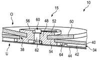
図1は、サブストレート(図示せず)収納用の空のカートリッジ12に挿入されたエンドエフェクタ10を示す。
FIG. 1 shows an
エンドエフェクタ10は、一連の動作要素の最後のロボット部品である。図示されたエンドエフェクタ10は、ウェーハなどのサブストレートをピックアップし搬送するためのホルダ又はグリッパである。そのために、エンドエフェクタは、ロボットの腕(図示せず)に接続可能である。
The
エンドエフェクタ10は、本体14および2つの保持器具15を有し、本体14は受入端16および取付端18を有する。
The
フランジ領域20は、取付端18に提供され、フランジ領域でフランジ板22が本体14に取り付けられる。フランジ板22は、エンドエフェクタ10をロボットの腕に取り付ける役割を果たす。
A
受入端16において、サブストレート(図1に破線で示されている)を保持するための保持領域24は、エンドエフェクタ10の上側Oにおいて形成される。図2において、円形サブストレートの中心点Mは、保持領域24においてサブストレートの受け入れが意図されている場所を示す。
At the receiving
切欠き部26は、受入端16から取付端18に向かって本体14の中に延びる。
The
切欠き部26は、まず受入端16から延びる2つの平行な横壁28を有し、それらの横壁は次に移行領域30で互いに接続する。この第一の実施形態においては、移行領域30は半径R1の半円である。
The
特に、切欠き部26は、本体14の取付端18の逆側にある本体14のU字型隙間である。
In particular, the
本体14の保持アーム32は切欠き部26によって形成され、平行な横壁28は本体の内側である。
The holding
加えて、流体チャンネル34が本体14内に形成され、フランジ領域20、すなわち取付端18から受入端16の方向に延びる。
In addition, a
図示されている実施形態において、流体チャンネル34は、負圧チャンネルである。しかし、流体チャンネル34はまた、過剰圧力チャンネルであってもよい。
In the illustrated embodiment, the
図2に示されるとおり、流体チャンネル34はフランジ領域20から始まり、保持領域24で保持アーム32の中まで延びる2つの支流36に分岐する。
As shown in FIG. 2, the
流体チャンネル34は、全体としてY字形状又はチューニング用音叉の形であり、2つの支流36が流体チャンネル34のU字形状部分を形成する。したがって、Uの両肢は、保持アーム32に延びる支流36の部分によって形成される。
The
支流36の終わりには本体14にそれぞれ開口部38が設置され、流体チャンネル34は保持領域24で上側Oから流出する。
保持器具15が開口部38に取り付けられる。したがって、保持器具15は、保持アーム32に設置されてもよい。したがって、少なくとも1つの開口部38が保持アーム32ごとに設置される。
A holding
図3は、本体14の分解図である。図示されている実施形態において、本体14は、上の層40、中間の層42および下の層44の3つの層を有する。上の層40および下の層44はそれぞれ本体14の外部層を形成する。
FIG. 3 is an exploded view of the
これらの3つの層40、42、44は全て同じ外形であり互いに固定されている。例えば、層40、42、44は互いに接着されている、および加えてねじ留めされていてもよい。3つの層40、42、44はまた、互いに溶接されてもよい。
These three
層40、42、44が同一の外形を有する構成であるために、切欠き部26は全ての層40、42、44を貫通して延びる。
Since the
下の層44は、全域で閉じており、中間の層42は流体チャンネル34を形成するためのスロット46を有し、上の層40も2つの開口部38を有する以外は全域で閉じている。
The
全ての層40、42、44は加えてねじ用の穴を有してもよい。 All layers 40, 42, 44 may additionally have holes for screws.
例えば、上の層40および中間の層42はそれぞれ金属板から製造される。例えば、高級鋼又はモリブデンが適当な材料である。
For example, the
いずれの場合も、上の層40と中間の層42を合わせると、金属板の材料特性により、保持領域24においてこれら2つの層40、42によってサブストレートが保持可能であるために十分に高いレベルの安定性を有する。当然、エンドエフェクタ10が全体として設計されたサイズのサブストレートを使用する場合を想定している。
In any case, when the
対照的に、下の層44は本来強くない、すなわちこの層単独では保持領域24において対応するサイズのサブストレートを保持できない。
In contrast, the
下の層は合成材料の膜から製造されてもよい。例えばポリエーテルエーテルケトン(PEEK)が適当な合成材料である。 The lower layer may be made from a film of synthetic material. For example, polyether ether ketone (PEEK) is a suitable synthetic material.
例えば、下の層44は0.1ミリメートル又はそれ以下の厚みを有する。
For example, the
流体チャンネル34を形成するために、流体チャンネル34の形状にあるスロット46が中間の層42に設置される。したがって、スロット46は、同様にY字形状又はチューニング用音叉の形である。
To form the
本体14が組み立てられた状態の場合、このスロット46は上および下から、すなわち垂直方向に上の層40および下の層44によって気密に完全に(開口部38およびフランジ板22の領域に提供される連結開口部を除いて)カバーされて閉じられる。
When the
流体チャンネル34は、上の層40に開口部38が設置される領域で、中間の層42のスロット46の端で終わる。
The
図4に示されるとおり、保持器具15の1つが、図示の開口部38内に取り付けられる。
As shown in FIG. 4, one of the
図示の実施形態において、保持器具15は吸引器具、特に真空吸引カップであり、キャリヤ48およびキャリヤ48に取り付けられた密封口50を有する。
In the illustrated embodiment, the holding
キャリヤ48は2つの円筒形部分、すなわち基礎部52および取付部54を有し、取付部54の直径は基礎部の直径よりも大きく、また開口部38の直径よりも大きい。
The
取付部54は、中間の層42の厚みに実質的に一致する厚みを有し、上の層40と下の層44の間に設置される。
The
基礎部52は、開口部38を貫通して延び、その上側、すなわち取付部54の逆側、に接触面56を有する。
The
吸引溝60が接触面56に提供され、キャリヤ48の中の貫通チャンネル62によって、および取付部54の中の連結チャンネル64によって、流体チャンネル34と流体連通している。
A
密封口50は、本体14の上側Oにおいて基礎部52に取り付けられ、接触面56を完全に包囲する。
The sealing
キャリヤ48は、中間の層42および上の層40を貫通して下の層44によって保持されることによりその場所でエンドエフェクタ10に取り付けられる。それはさらに、上の層40の上側に支えられる密封口50によって固定される。
The
サブストレートをピックアップするために、エンドエフェクタ10はサブストレートに向かって下から移動され、サブストレートを持ち上げてもよい。同時に、負圧チャンネルとして機能する流体チャンネル34によって吸引溝60に負の圧力をかける真空源(図示せず)によってサブストレートに吸引力が適用されてもよい。
To pick up the substrate, the
サブストレートは続いて、大気圧からの過剰圧力によって接触面56に押し付けられ、それによりエンドエフェクタ10にしっかりと固定される。サブストレートはそのとき、少なくとも接触面56の上で保持領域24に対して接触している。
The substrate is then pressed against the
保持器具15をベルヌーイ効果に基づく固定器具として設計することもまた可能である。この場合、過剰圧力源(図示せず)を使って、高圧気体が流体チャンネル34に供給され、高速で保持器具15から流れ出し、サブストレートを素早く超えて流れる。これによりエンドエフェクタ10に向かう力がサブストレートにかかり、サブストレートがエンドエフェクタ10に固定される。流体チャンネル34はこの場合、過剰圧力チャンネルである。
It is also possible to design the holding
加えて、支持面65を保持アーム32の上、特に受入端16に向いた端に形成してもよい。支持面65は例えばゴムなどの柔らかい材料で製造されてもよい。最適の場合、サブストレートはエンドエフェクタ10に固定されるとき、支持面65に接触する。
In addition, the
下の層44は本来強くないが、本体14の積層構造により全体として安定したエンドエフェクタ10が得られる。これは、このエンドエフェクタ10用のサイズで提供されたサブストレートを保持領域24において搬送可能であるために十分安定しているということである。下の層44が本来強くない薄膜で形成されていることにより、エンドエフェクタ10の厚みは、特に保持領域24において、明らかに低減される。
Although the
図5および図6は本願発明に係るエンドエフェクタ10の第二の実施形態を示し、それは実質的に第一の実施形態に一致する。したがって、ここからは相違点だけが記述され、同等で機能的に等価な部品には同じ参照符号が使われる。
5 and 6 show a second embodiment of the
第二の実施形態で図示されるエンドエフェクタ10は、第一の実施形態のエンドエフェクタ10よりも大きいサブストレート用に設計され、したがって第二の実施形態の部品は寸法が異なる。
The
例えば、より大きいサブストレートをより安定して保持する目的で、接触面56同士の間隔を大きくするために本体14の幅が広い。同時に切欠き部26も幅が広い。
For example, the width of the
図5は、第二の実施形態のエンドエフェクタ10を下から見た図であり、明確さのためにフランジ22は省略されている。
FIG. 5 is a view of the
この実施形態において、本体14は2つの層、すなわち上の層66および下の層68のみを有する。
In this embodiment, the
下の層68は、第一の実施形態の下の層44に対応し、第一の実施形態の下の層44と同一である。
The
対照的に、上の層66は、第一の実施形態の上の層40と中間の層42の組み合わせに対応する。
In contrast, the
流体チャンネル34の輪郭を部分的に定める溝70は、上の層66の下側に組み込まれる。したがって溝70は第一の実施形態のスロット46に対応し、溝70は下の層68によって閉じられて流体チャンネル34が形成される。
A
加えて、上の層66は、エンドエフェクタ110の上側Oに向かう流体チャンネル34の開口部38を含む。
In addition, the
上の層66はまた保持器具15の取付部54用に凹部を含んでもよい。
図解目的で、図5には下の層68が透明であるかのように示され、上の層66の溝70が見えている。
For illustration purposes, FIG. 5 shows the
第一の実施形態と対照的に、切欠き部26の移行領域30は半円ではなく、それぞれが四分円を描くR面取りR2を2つ有する。2つの四分円は短い直線部72によってつながる(図6を参照)。
In contrast to the first embodiment, the transition region 30 of the
当然、図解された実施形態の2つの特徴は互いに組み合わせることができる。特に、第一の実施形態のエンドエフェクタ10は2層で形成可能であり、第二の実施形態のエンドエフェクタは3層で形成可能である。
Of course, the two features of the illustrated embodiment can be combined with each other. In particular, the
同様に、エンドエフェクタの本体の層が全てそれぞれ本来強くなく、サブストレートを保持するために必要な強さはこれらの層を組み合わせることによってのみ達成されるということも可能である。 Similarly, it is possible that all layers of the body of the end effector are not inherently strong and that the strength required to hold the substrate is achieved only by combining these layers.
図7は、3つの異なるサイズのエンドエフェクタ10を、対応するサイズのサブストレート用カートリッジ12と共に示す。例えば、左側に示されるサイズは第一の実施形態のサイズに対応し、中央に示されるサイズは第二の実施形態のサイズに対応する。さらに、特に大きいサブストレート用のより大きいサイズが右側に示される。
FIG. 7 shows three different
例えば、左側のエンドエフェクタは、直径100ミリメートル以上のサブストレート用に設計され、中央のエンドエフェクタは、直径150ミリメートル以上のサブストレート用に設計され、右側のエンドエフェクタは、直径200ミリメートル以上のサブストレート用に設計されている。 For example, the left end effector is designed for a substrate having a diameter of 100 millimeters or more, the middle end effector is designed for a substrate having a diameter of 150 millimeters or more, and the right end effector is a substrate having a diameter of 200 millimeters or more. Designed for straight use.
当然、ウェーハの特性によっては、同じグリッパを異なるサイズのウェーハにも使用することができる。 Of course, depending on the properties of the wafer, the same gripper can be used for different size wafers.
エンドエフェクタを製造するために、例えばレーザやウォータージェットによって個々の層が同時に切断されてもよい。これによれば、層が完全に同一の外形を持つことが確かとなる。複数の層を機械的に連結するために使われる開口部もまた、連結される複数の層を重ねあわせた状態で1つの工程で同時に加工されてもよい。 In order to produce an end effector, the individual layers may be cut simultaneously, for example by means of a laser or a water jet. This ensures that the layers have the exact same contour. The openings used to mechanically connect the multiple layers may also be processed simultaneously in one step with the connected multiple layers superimposed.
Claims (16)
Applications Claiming Priority (2)
| Application Number | Priority Date | Filing Date | Title |
|---|---|---|---|
| NL2018244 | 2017-01-27 | ||
| NL2018244A NL2018244B1 (en) | 2017-01-27 | 2017-01-27 | Endeffektor |
Publications (3)
| Publication Number | Publication Date |
|---|---|
| JP2018174302A true JP2018174302A (en) | 2018-11-08 |
| JP2018174302A5 JP2018174302A5 (en) | 2019-12-26 |
| JP7109927B2 JP7109927B2 (en) | 2022-08-01 |
Family
ID=58606566
Family Applications (1)
| Application Number | Title | Priority Date | Filing Date |
|---|---|---|---|
| JP2018011616A Active JP7109927B2 (en) | 2017-01-27 | 2018-01-26 | end effector |
Country Status (9)
| Country | Link |
|---|---|
| US (1) | US10343292B2 (en) |
| JP (1) | JP7109927B2 (en) |
| KR (1) | KR20180088597A (en) |
| CN (1) | CN108364896A (en) |
| AT (1) | AT519588B1 (en) |
| DE (1) | DE102018100855A1 (en) |
| NL (1) | NL2018244B1 (en) |
| SG (1) | SG10201800713TA (en) |
| TW (1) | TWI710437B (en) |
Cited By (1)
| Publication number | Priority date | Publication date | Assignee | Title |
|---|---|---|---|---|
| JP7333114B2 (en) | 2021-06-16 | 2023-08-24 | 盛詮科技股▲フン▼有限公司 | Air floating wafer transfer arm |
Families Citing this family (9)
| Publication number | Priority date | Publication date | Assignee | Title |
|---|---|---|---|---|
| JP7175735B2 (en) * | 2018-12-11 | 2022-11-21 | 平田機工株式会社 | Substrate carrier |
| EP3896385B1 (en) * | 2018-12-11 | 2024-01-17 | Rorze Corporation | Electrostatic capacitance sensor |
| US11574837B2 (en) | 2020-06-12 | 2023-02-07 | Taiwan Semiconductor Manufacturing Co., Ltd. | Robot blade having multiple sensors for multiple different alignment tasks |
| FR3112980B1 (en) * | 2020-07-28 | 2022-07-22 | Defitech | Suction box for a gripper |
| USD949219S1 (en) * | 2020-08-20 | 2022-04-19 | Grey Orange Pte. Ltd. | Spatula gripper |
| EP4273911A1 (en) | 2022-05-03 | 2023-11-08 | Werner Lieb GmbH | Holding device and method for holding and/or transporting workpieces and/or components, optionally with tool-free replaceable suction elements |
| TWI826206B (en) * | 2022-12-07 | 2023-12-11 | 緯創資通股份有限公司 | Wafer handling equipment and sucker module thereof |
| CN115632023B (en) * | 2022-12-22 | 2023-08-04 | 河北博特半导体设备科技有限公司 | Double-arm wafer transmission device |
| TWI814679B (en) * | 2023-02-13 | 2023-09-01 | 盛詮科技股份有限公司 | Carrier suspended arm |
Citations (3)
| Publication number | Priority date | Publication date | Assignee | Title |
|---|---|---|---|---|
| JPH09139413A (en) * | 1995-11-14 | 1997-05-27 | Du Pont Kk | Wafer carrying parts and wafer carrying device |
| JPH11354607A (en) * | 1998-06-10 | 1999-12-24 | Mitsubishi Chemical Corp | Hand for transfer apparatus |
| JP2004186355A (en) * | 2002-12-03 | 2004-07-02 | Nikon Corp | Suction holding member and apparatus thereof |
Family Cites Families (20)
| Publication number | Priority date | Publication date | Assignee | Title |
|---|---|---|---|---|
| US4620738A (en) * | 1985-08-19 | 1986-11-04 | Varian Associates, Inc. | Vacuum pick for semiconductor wafers |
| US5226636A (en) * | 1992-06-10 | 1993-07-13 | International Business Machines Corporation | Holding fixture for substrates |
| EP0634787B1 (en) * | 1993-07-15 | 1997-05-02 | Applied Materials, Inc. | Subsrate tray and ceramic blade for semiconductor processing apparatus |
| US6244641B1 (en) * | 1999-12-02 | 2001-06-12 | M.E.C. Technology, Inc. | Wafer transfer arm |
| JP2003168718A (en) * | 2001-11-30 | 2003-06-13 | Murata Mach Ltd | Single wafer transfer device |
| AU2002361894A1 (en) * | 2002-07-29 | 2004-02-16 | E. I. Du Pont De Nemours And Company | Carbon fiber composite transfer member with reflective surfaces |
| US6942265B1 (en) * | 2002-10-23 | 2005-09-13 | Kla-Tencor Technologies Corporation | Apparatus comprising a flexible vacuum seal pad structure capable of retaining non-planar substrates thereto |
| US20050110292A1 (en) * | 2002-11-26 | 2005-05-26 | Axcelis Technologies, Inc. | Ceramic end effector for micro circuit manufacturing |
| US7055875B2 (en) * | 2003-07-11 | 2006-06-06 | Asyst Technologies, Inc. | Ultra low contact area end effector |
| DE102006031434B4 (en) * | 2006-07-07 | 2019-11-14 | Erich Thallner | Handling device and handling method for wafers |
| US20080247857A1 (en) * | 2007-04-05 | 2008-10-09 | Ichiro Yuasa | End effector and robot for transporting substrate |
| JP2009285823A (en) * | 2008-05-28 | 2009-12-10 | Meian Kokusai Gigyo Kofun Yugenkoshi | Robot arm, component of its holding means, and manufacturing method of the component |
| JP2011110682A (en) * | 2009-11-30 | 2011-06-09 | Jx Nippon Oil & Energy Corp | Robot hand and method of manufacturing the same |
| US9187256B2 (en) * | 2011-08-24 | 2015-11-17 | Harmotec Co., Ltd. | Non-contacting conveyance equipment |
| JP2013078810A (en) * | 2011-10-03 | 2013-05-02 | Smc Corp | Vacuum suction apparatus |
| TWI611997B (en) * | 2013-09-26 | 2018-01-21 | 應用材料股份有限公司 | Pneumatic end effector apparatus and substrate transportation systems for transporting substrates |
| JP6216219B2 (en) | 2013-11-07 | 2017-10-18 | 一般財団法人ファインセラミックスセンター | Thermal insulation structure |
| US20150290815A1 (en) * | 2014-04-11 | 2015-10-15 | Varian Semiconductor Equipment Associates, Inc. | Planar end effector and method of making a planar end effector |
| US9415519B2 (en) * | 2014-07-01 | 2016-08-16 | Varian Semiconductor Equipment Associates, Inc. | Composite end effector and method of making a composite end effector |
| US20160254176A1 (en) * | 2015-02-27 | 2016-09-01 | AZSimilate, LLC | Positive Pressure Bernoulli Wand with Coiled Path |
-
2017
- 2017-01-27 NL NL2018244A patent/NL2018244B1/en active
-
2018
- 2018-01-16 DE DE102018100855.4A patent/DE102018100855A1/en active Pending
- 2018-01-19 US US15/875,708 patent/US10343292B2/en active Active
- 2018-01-22 TW TW107102183A patent/TWI710437B/en active
- 2018-01-24 AT ATA50058/2018A patent/AT519588B1/en active
- 2018-01-26 KR KR1020180009853A patent/KR20180088597A/en not_active Application Discontinuation
- 2018-01-26 JP JP2018011616A patent/JP7109927B2/en active Active
- 2018-01-26 SG SG10201800713TA patent/SG10201800713TA/en unknown
- 2018-01-29 CN CN201810083865.7A patent/CN108364896A/en active Pending
Patent Citations (3)
| Publication number | Priority date | Publication date | Assignee | Title |
|---|---|---|---|---|
| JPH09139413A (en) * | 1995-11-14 | 1997-05-27 | Du Pont Kk | Wafer carrying parts and wafer carrying device |
| JPH11354607A (en) * | 1998-06-10 | 1999-12-24 | Mitsubishi Chemical Corp | Hand for transfer apparatus |
| JP2004186355A (en) * | 2002-12-03 | 2004-07-02 | Nikon Corp | Suction holding member and apparatus thereof |
Cited By (1)
| Publication number | Priority date | Publication date | Assignee | Title |
|---|---|---|---|---|
| JP7333114B2 (en) | 2021-06-16 | 2023-08-24 | 盛詮科技股▲フン▼有限公司 | Air floating wafer transfer arm |
Also Published As
| Publication number | Publication date |
|---|---|
| TW201829140A (en) | 2018-08-16 |
| SG10201800713TA (en) | 2018-08-30 |
| AT519588B1 (en) | 2021-10-15 |
| NL2018244B1 (en) | 2018-08-07 |
| DE102018100855A1 (en) | 2018-08-02 |
| JP7109927B2 (en) | 2022-08-01 |
| CN108364896A (en) | 2018-08-03 |
| US20180215048A1 (en) | 2018-08-02 |
| KR20180088597A (en) | 2018-08-06 |
| US10343292B2 (en) | 2019-07-09 |
| AT519588A2 (en) | 2018-08-15 |
| AT519588A3 (en) | 2020-02-15 |
| TWI710437B (en) | 2020-11-21 |
Similar Documents
| Publication | Publication Date | Title |
|---|---|---|
| JP2018174302A (en) | End effector | |
| US10259124B2 (en) | Suction apparatus for an end effector, end effector for holding substrates and method of producing an end effector | |
| JP5379589B2 (en) | Vacuum suction pad, transfer arm and substrate transfer device | |
| US10504762B2 (en) | Bridging front opening unified pod (FOUP) | |
| EP3605597B1 (en) | Silicon chip holding device, silicon chip conveying device, silicon chip delivery system and conveying method | |
| US20180012790A1 (en) | Substrate carrier | |
| JP4797013B2 (en) | Bonding device | |
| JP7364692B2 (en) | Substrate suction holding structure and substrate transfer robot | |
| KR102002553B1 (en) | Lightweight vacuum chuck for precise transfer of semiconductor wafers | |
| JP5202028B2 (en) | Vacuum tweezers, substrate transfer apparatus and substrate processing apparatus using the same | |
| JP2022051595A (en) | Vacuum suction chuck | |
| JP2013143518A (en) | Placement structure of substrate and plasma processing apparatus | |
| US20150279720A1 (en) | End effector pads | |
| KR101684739B1 (en) | Wafer transfer apparatus | |
| EP3655352A1 (en) | Non-contact handler and method of handling workpieces using the same | |
| JP2012164748A (en) | Wafer protection jig and wafer handling method | |
| CN111989196B (en) | Clamping device | |
| JPH01206643A (en) | Substrate attracting structure | |
| WO2020013013A1 (en) | Transportation hand | |
| JPH09225768A (en) | Board holding device | |
| JP2009006441A (en) | Vacuum tweezers, substrate carrier device using it and substrate treatment device | |
| CN112077830A (en) | Robot arm | |
| KR20160060922A (en) | Apparatus for transferring semiconductor packages |
Legal Events
| Date | Code | Title | Description |
|---|---|---|---|
| A521 | Request for written amendment filed |
Free format text: JAPANESE INTERMEDIATE CODE: A523 Effective date: 20191115 |
|
| A621 | Written request for application examination |
Free format text: JAPANESE INTERMEDIATE CODE: A621 Effective date: 20191115 |
|
| A977 | Report on retrieval |
Free format text: JAPANESE INTERMEDIATE CODE: A971007 Effective date: 20201211 |
|
| A131 | Notification of reasons for refusal |
Free format text: JAPANESE INTERMEDIATE CODE: A131 Effective date: 20201215 |
|
| A521 | Request for written amendment filed |
Free format text: JAPANESE INTERMEDIATE CODE: A523 Effective date: 20210311 |
|
| A02 | Decision of refusal |
Free format text: JAPANESE INTERMEDIATE CODE: A02 Effective date: 20210608 |
|
| A521 | Request for written amendment filed |
Free format text: JAPANESE INTERMEDIATE CODE: A523 Effective date: 20211008 |
|
| C60 | Trial request (containing other claim documents, opposition documents) |
Free format text: JAPANESE INTERMEDIATE CODE: C60 Effective date: 20211008 |
|
| A911 | Transfer to examiner for re-examination before appeal (zenchi) |
Free format text: JAPANESE INTERMEDIATE CODE: A911 Effective date: 20211018 |
|
| C21 | Notice of transfer of a case for reconsideration by examiners before appeal proceedings |
Free format text: JAPANESE INTERMEDIATE CODE: C21 Effective date: 20211019 |
|
| A912 | Re-examination (zenchi) completed and case transferred to appeal board |
Free format text: JAPANESE INTERMEDIATE CODE: A912 Effective date: 20211210 |
|
| C211 | Notice of termination of reconsideration by examiners before appeal proceedings |
Free format text: JAPANESE INTERMEDIATE CODE: C211 Effective date: 20211214 |
|
| C22 | Notice of designation (change) of administrative judge |
Free format text: JAPANESE INTERMEDIATE CODE: C22 Effective date: 20220329 |
|
| C22 | Notice of designation (change) of administrative judge |
Free format text: JAPANESE INTERMEDIATE CODE: C22 Effective date: 20220405 |
|
| C23 | Notice of termination of proceedings |
Free format text: JAPANESE INTERMEDIATE CODE: C23 Effective date: 20220531 |
|
| C03 | Trial/appeal decision taken |
Free format text: JAPANESE INTERMEDIATE CODE: C03 Effective date: 20220628 |
|
| C30A | Notification sent |
Free format text: JAPANESE INTERMEDIATE CODE: C3012 Effective date: 20220628 |
|
| A61 | First payment of annual fees (during grant procedure) |
Free format text: JAPANESE INTERMEDIATE CODE: A61 Effective date: 20220720 |
|
| R150 | Certificate of patent or registration of utility model |
Ref document number: 7109927 Country of ref document: JP Free format text: JAPANESE INTERMEDIATE CODE: R150 |