JP2018129405A5 - - Google Patents
Download PDFInfo
- Publication number
- JP2018129405A5 JP2018129405A5 JP2017021716A JP2017021716A JP2018129405A5 JP 2018129405 A5 JP2018129405 A5 JP 2018129405A5 JP 2017021716 A JP2017021716 A JP 2017021716A JP 2017021716 A JP2017021716 A JP 2017021716A JP 2018129405 A5 JP2018129405 A5 JP 2018129405A5
- Authority
- JP
- Japan
- Prior art keywords
- lead
- dam bar
- etched
- width
- etching
- Prior art date
- Legal status (The legal status is an assumption and is not a legal conclusion. Google has not performed a legal analysis and makes no representation as to the accuracy of the status listed.)
- Granted
Links
- 238000005530 etching Methods 0.000 description 2
- 238000004519 manufacturing process Methods 0.000 description 1
- 239000000463 material Substances 0.000 description 1
- 239000002184 metal Substances 0.000 description 1
- 230000001629 suppression Effects 0.000 description 1
Images
Description
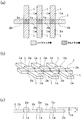
しかし、特許文献1に記載のリードフレームは、例えば、図3や図4に示すような、ダムバー50にハーフエッチングを施す部位の幅をダムバー50の幅より短くする構成は、ダムバー50の幅が小さいリードフレームには適用することが難しい。また、ハーフエッチングを施す部位の数やハーフエッチングの幅にバリエーションを持たせることができず、設計の自由度が制限されてしまう。
また、例えば、図5に示すような、ダムバー50の長手方向にわたってハーフエッチングを施す部位と施さない個所を設ける構成の場合であっても、ハーフエッチングを施す面が、材料である金属板の一方の側の面に偏っているため、ダムバー50の変形を十分に抑えることができない。しかも、ハーフエッチング部よりも厚い部分となる第2の部位52全てがハーフエッチングされずに残るため、その分、ダムバー50を切断するブレードが目詰まりを起こし易くなり、連続加工時間が延び難い。
更には、リードにおけるダムバーに連結される端部と、ダムバーにおけるリードの端部と連結する部位との全てにハーフエッチングが施されていると、リードが細長い或いは屈曲している場合、リードの先端の例えば端子となる部分に段差を生じ易く、リードフレームの製造過程で、搬送時の引っ掛かり等により、リードが連結された切断対象となる最も細いサポートリードに対し過剰な負荷がかかり、ねじれ変形を生じる虞がある。
However, in the lead frame described in
Further, for example, as shown in FIG. 5, even in the case of a configuration in which a portion to be half-etched and a portion not to be subjected are provided in the longitudinal direction of the dam bar 50, the surface to be half-etched is one of the metal plates that are materials. Therefore, the deformation of the dam bar 50 cannot be sufficiently suppressed. Moreover, since the second portion 52 of all of the thick portion than half etching portion is left without being half-etched in g, correspondingly, easily cause blade clogging of cutting the dam bar 50, hardly extends continuous processing time .
Furthermore, when the lead is connected to the end of the dam bar and the portion of the dam bar connected to the end of the lead is half-etched, if the lead is elongated or bent, the tip of the lead For example, it is easy to make a step in the part that becomes a terminal, and in the lead frame manufacturing process, excessive load is applied to the thinnest support lead to be cut to which the lead is connected due to catching at the time of conveyance, etc. May occur.
Priority Applications (4)
| Application Number | Priority Date | Filing Date | Title |
|---|---|---|---|
| JP2017021716A JP6798670B2 (en) | 2017-02-08 | 2017-02-08 | Lead frame and its manufacturing method |
| US15/891,755 US10304760B2 (en) | 2017-02-08 | 2018-02-08 | Lead frame and method for manufacturing the same |
| MYPI2018700506A MY192268A (en) | 2017-02-08 | 2018-02-08 | Lead frame and method for manufacturing the same |
| CN201810127202.0A CN108417553B (en) | 2017-02-08 | 2018-02-08 | Lead frame and method for manufacturing the same |
Applications Claiming Priority (1)
| Application Number | Priority Date | Filing Date | Title |
|---|---|---|---|
| JP2017021716A JP6798670B2 (en) | 2017-02-08 | 2017-02-08 | Lead frame and its manufacturing method |
Publications (3)
| Publication Number | Publication Date |
|---|---|
| JP2018129405A JP2018129405A (en) | 2018-08-16 |
| JP2018129405A5 true JP2018129405A5 (en) | 2019-11-21 |
| JP6798670B2 JP6798670B2 (en) | 2020-12-09 |
Family
ID=63037345
Family Applications (1)
| Application Number | Title | Priority Date | Filing Date |
|---|---|---|---|
| JP2017021716A Active JP6798670B2 (en) | 2017-02-08 | 2017-02-08 | Lead frame and its manufacturing method |
Country Status (4)
| Country | Link |
|---|---|
| US (1) | US10304760B2 (en) |
| JP (1) | JP6798670B2 (en) |
| CN (1) | CN108417553B (en) |
| MY (1) | MY192268A (en) |
Families Citing this family (2)
| Publication number | Priority date | Publication date | Assignee | Title |
|---|---|---|---|---|
| US11545418B2 (en) * | 2018-10-24 | 2023-01-03 | Texas Instruments Incorporated | Thermal capacity control for relative temperature-based thermal shutdown |
| US11581195B2 (en) * | 2020-12-21 | 2023-02-14 | Alpha And Omega Semiconductor International Lp | Semiconductor package having wettable lead flank and method of making the same |
Family Cites Families (14)
| Publication number | Priority date | Publication date | Assignee | Title |
|---|---|---|---|---|
| US6700186B2 (en) * | 2000-12-21 | 2004-03-02 | Mitsui High-Tec, Inc. | Lead frame for a semiconductor device, a semiconductor device made from the lead frame, and a method of making a semiconductor device |
| KR20020093250A (en) * | 2001-06-07 | 2002-12-16 | 삼성전자 주식회사 | ELP type leadframe and ELP using the same |
| US7259460B1 (en) * | 2004-06-18 | 2007-08-21 | National Semiconductor Corporation | Wire bonding on thinned portions of a lead-frame configured for use in a micro-array integrated circuit package |
| US7968377B2 (en) * | 2005-09-22 | 2011-06-28 | Stats Chippac Ltd. | Integrated circuit protruding pad package system |
| JP5214911B2 (en) * | 2006-12-27 | 2013-06-19 | 株式会社デンソー | Mold package manufacturing method |
| JP2009088412A (en) * | 2007-10-02 | 2009-04-23 | Renesas Technology Corp | Manufacturing method of semiconductor device |
| JP5899614B2 (en) * | 2010-11-26 | 2016-04-06 | 大日本印刷株式会社 | Leadframe and leadframe manufacturing method |
| JP6087153B2 (en) * | 2013-01-10 | 2017-03-01 | 株式会社三井ハイテック | Lead frame |
| JP6143468B2 (en) * | 2013-01-11 | 2017-06-07 | 株式会社三井ハイテック | Lead frame |
| KR101486790B1 (en) * | 2013-05-02 | 2015-01-28 | 앰코 테크놀로지 코리아 주식회사 | Micro Lead Frame for semiconductor package |
| JP6319644B2 (en) * | 2013-10-01 | 2018-05-09 | 大日本印刷株式会社 | Lead frame, manufacturing method thereof, and manufacturing method of semiconductor device |
| US9252063B2 (en) * | 2014-07-07 | 2016-02-02 | Infineon Technologies Ag | Extended contact area for leadframe strip testing |
| CN104659010B (en) * | 2015-02-11 | 2018-03-16 | 江苏长电科技股份有限公司 | A kind of lead frame structure and package body structure of square flat pinless encapsulation |
| JP6603538B2 (en) * | 2015-10-23 | 2019-11-06 | 新光電気工業株式会社 | Lead frame and manufacturing method thereof |
-
2017
- 2017-02-08 JP JP2017021716A patent/JP6798670B2/en active Active
-
2018
- 2018-02-08 MY MYPI2018700506A patent/MY192268A/en unknown
- 2018-02-08 CN CN201810127202.0A patent/CN108417553B/en active Active
- 2018-02-08 US US15/891,755 patent/US10304760B2/en active Active
Similar Documents
| Publication | Publication Date | Title |
|---|---|---|
| USD942406S1 (en) | Electric terminal | |
| USD801485S1 (en) | Faucet | |
| USD787640S1 (en) | Handle | |
| USD861838S1 (en) | Sink | |
| USD770020S1 (en) | Sink | |
| USD772306S1 (en) | Mixing drum | |
| USD858243S1 (en) | Demolition tool | |
| USD809631S1 (en) | Faucet | |
| JP2015027563A5 (en) | ||
| USD782018S1 (en) | Sink | |
| JP2017520899A5 (en) | ||
| JP2018129405A5 (en) | ||
| USD886255S1 (en) | Sink apron | |
| USD724712S1 (en) | Toilet | |
| USD767744S1 (en) | Toilet | |
| JP2019079674A5 (en) | ||
| USD725757S1 (en) | Sink | |
| JP2021150099A5 (en) | ||
| KR101465971B1 (en) | Bending device for metal plate | |
| JP2016029651A5 (en) | ||
| JP2013093477A5 (en) | ||
| JP2015012177A5 (en) | Semiconductor device | |
| TW201810586A (en) | Lead frame | |
| FR3010356B1 (en) | ASSEMBLY FOR A SEAT FRAME, SEAT FRAME AND METHOD FOR MANUFACTURING SUCH AN ASSEMBLY. | |
| JP2021072389A5 (en) |