JP2018109550A - Electronic component conveyance device and electronic component inspection device - Google Patents
Electronic component conveyance device and electronic component inspection device Download PDFInfo
- Publication number
- JP2018109550A JP2018109550A JP2016257051A JP2016257051A JP2018109550A JP 2018109550 A JP2018109550 A JP 2018109550A JP 2016257051 A JP2016257051 A JP 2016257051A JP 2016257051 A JP2016257051 A JP 2016257051A JP 2018109550 A JP2018109550 A JP 2018109550A
- Authority
- JP
- Japan
- Prior art keywords
- unit
- electronic component
- image
- imaging
- inspection
- Prior art date
- Legal status (The legal status is an assumption and is not a legal conclusion. Google has not performed a legal analysis and makes no representation as to the accuracy of the status listed.)
- Pending
Links
Images


Landscapes
- Length Measuring Devices By Optical Means (AREA)
- Testing Of Individual Semiconductor Devices (AREA)
Abstract
Description
本発明は、電子部品搬送装置および電子部品検査装置に関する。 The present invention relates to an electronic component conveying device and an electronic component inspection device.
従来から、例えばICデバイス等の電子部品の電気的特性を検査する電子部品検査装置が知られており、この電子部品検査装置には、ICデバイスを搬送するための電子部品搬送装置が組み込まれている(例えば、特許文献1参照)。 2. Description of the Related Art Conventionally, an electronic component inspection apparatus that inspects electrical characteristics of electronic components such as IC devices is known, and an electronic component conveyance apparatus for conveying an IC device is incorporated in the electronic component inspection apparatus. (For example, refer to Patent Document 1).
特許文献1に記載されている電子部品搬送装置では、電子部品の搬送が行われていない状態において、電子部品の検査を行うソケット(検査部)の画像を撮像し、その画像が基準画像データとして予め記憶されている。そして、電子部品の搬送中にソケットの画像を撮像し、その画像を前記基準画像データと比較するよう構成されている。これにより、ソケットにおける搬送異常等を検出することができる。
In the electronic component conveying apparatus described in
しかしながら、特許文献1に記載の電子部品検査装置では、搬送部(ハンド)とソケットとの位置関係等によっては、搬送部によって遮られ、ソケットを撮像するのが困難となる。その結果、ソケットにおける搬送異常等を見落とす可能性が有る。
However, in the electronic component inspection apparatus disclosed in
本発明は、上述の課題の少なくとも一部を解決するためになされたものであり、以下のものとして実現することが可能である。 SUMMARY An advantage of some aspects of the invention is to solve at least a part of the problems described above, and the invention can be implemented as follows.
本発明の電子部品搬送装置は、電子部品を載置する載置部を有する電子部品載置部を配置可能で、
第1方向と、前記第1方向と異なる第2方向とに移動可能であり、電子部品を把持可能な第1把持部と、
前記第1方向および前記第2方向に移動可能であり、電子部品を把持可能な第2把持部と、
前記第1把持部および前記第2把持部の間から前記電子部品載置部を撮像可能な撮像部と、
前記第1把持部および前記第2把持部のうちの少なくとも1つの把持部の位置情報を検出可能な位置検出部と、を有し、
前記第1把持部および前記第2把持部は、前記撮像部に対して第2方向に移動可能で、
前記撮像部は、前記位置検出部が検出した第1位置情報に基づいて前記電子部品載置部の第1像を撮像することを特徴とする。
The electronic component transport device of the present invention can arrange an electronic component placement portion having a placement portion for placing an electronic component,
A first gripper that is movable in a first direction and a second direction different from the first direction and capable of gripping an electronic component;
A second gripper that is movable in the first direction and the second direction and is capable of gripping an electronic component;
An imaging unit capable of imaging the electronic component placement unit from between the first holding unit and the second holding unit;
A position detection unit capable of detecting position information of at least one of the first gripping unit and the second gripping unit;
The first gripping part and the second gripping part are movable in a second direction with respect to the imaging part,
The imaging unit captures a first image of the electronic component placement unit based on first position information detected by the position detection unit.
これにより、把持部の位置情報に基づいて撮像を行うことができる。よって、第1把持部および第2把持部の間から電子部品載置部を撮像することができる。その結果、例えば、撮像結果に基づいて、載置部に電子部品が配置されているか否かを判断する場合、その判断をより正確に行うことができる。 Thereby, imaging can be performed based on the position information of the grip portion. Therefore, it is possible to take an image of the electronic component placement unit from between the first holding unit and the second holding unit. As a result, for example, when it is determined whether or not an electronic component is placed on the placement unit based on the imaging result, the determination can be made more accurately.
本発明の電子部品搬送装置では、前記撮像部に撮像された前記第1像に基づいて、第2位置情報を作成するのが好ましい。 In the electronic component transport device of the present invention, it is preferable that the second position information is created based on the first image picked up by the image pickup unit.
これにより、例えば、上記判断を行う場合、その判断により適した像を撮像することができる。 Thereby, for example, when the above determination is made, an image more suitable for the determination can be taken.
本発明の電子部品搬送装置では、前記第2位置情報は、前記第1位置情報とは異なるものであるのが好ましい。 In the electronic component transport device of the present invention, it is preferable that the second position information is different from the first position information.
これにより、例えば、上記判断を行う場合、その判断により適した像を撮像することができる。 Thereby, for example, when the above determination is made, an image more suitable for the determination can be taken.
本発明の電子部品搬送装置では、前記第2位置情報は、前記第1像に含まれる前記少なくとも1つの把持部の像と、前記第1像に含まれる前記載置部の像とに基づいて決められるのが好ましい。 In the electronic component transport device according to the aspect of the invention, the second position information is based on the image of the at least one gripping part included in the first image and the image of the placement part included in the first image. It is preferable to be determined.
これにより、例えば、上記判断を行う場合、その判断により適した像を撮像することができる。 Thereby, for example, when the above determination is made, an image more suitable for the determination can be taken.
本発明の電子部品搬送装置では、前記撮像部は、前記第2位置情報に基づいて、前記電子部品載置部の第2像を撮像するのが好ましい。 In the electronic component transport device according to the aspect of the invention, it is preferable that the imaging unit captures a second image of the electronic component placement unit based on the second position information.
これにより、例えば、上記判断を行う場合、その判断により適した像を撮像することができる。 Thereby, for example, when the above determination is made, an image more suitable for the determination can be taken.
本発明の電子部品搬送装置では、前記撮像部に撮像された前記第2像に基づいて、第3位置情報を作成するのが好ましい。 In the electronic component transport device of the present invention, it is preferable that the third position information is created based on the second image picked up by the image pickup unit.
これにより、例えば、上記判断を行う場合、その判断にさらに適した像を撮像することができる。 Thereby, for example, when the above determination is made, an image more suitable for the determination can be taken.
本発明の電子部品搬送装置では、前記第3位置情報は、前記第1位置情報および前記第2位置情報とは異なるものであるのが好ましい。 In the electronic component transport device of the present invention, it is preferable that the third position information is different from the first position information and the second position information.
これにより、例えば、上記判断を行う場合、その判断により適した像を撮像することができる。 Thereby, for example, when the above determination is made, an image more suitable for the determination can be taken.
本発明の電子部品搬送装置では、前記第3位置情報は、前記第2像に含まれる前記少なくとも1つの把持部の像と、前記第2像に含まれる前記載置部の像とに基づいて決められるのが好ましい。 In the electronic component transport device according to the aspect of the invention, the third position information is based on the image of the at least one gripping part included in the second image and the image of the mounting part included in the second image. It is preferable to be determined.
これにより、例えば、上記判断を行う場合、その判断にさらに適した像を撮像することができる。 Thereby, for example, when the above determination is made, an image more suitable for the determination can be taken.
本発明の電子部品搬送装置では、前記第1把持部と前記第2把持部との間を通して、前記電子部品載置部に光を照射可能に配置された光照射部を有するのが好ましい。 In the electronic component transport device of the present invention, it is preferable to have a light irradiation unit disposed between the first gripping unit and the second gripping unit so as to irradiate light to the electronic component mounting unit.
これにより、電子部品載置部に照射された光に基づいて、後述する判断を行うことができる。 Thereby, based on the light irradiated to the electronic component mounting part, the judgment mentioned later can be performed.
本発明の電子部品搬送装置では、前記撮像部に対して撮像指令信号を送信するタイミングを調整可能な制御部を有するのが好ましい。 In the electronic component conveying apparatus of the present invention, it is preferable to have a control unit capable of adjusting a timing at which an imaging command signal is transmitted to the imaging unit.
これにより、撮像部が撮像した画像において、載置部が映るよう調整することができる。 Thereby, it can adjust so that a mounting part may be reflected in the image which the imaging part imaged.
本発明の電子部品搬送装置では、前記制御部は、前記撮像部が撮像を開始するタイミングを調整可能であるのが好ましい。 In the electronic component transport device according to the aspect of the invention, it is preferable that the control unit can adjust a timing at which the imaging unit starts imaging.
これにより、撮像部が撮像した画像において、載置部が映るよう、正確に調整することができる。 Thereby, in the image which the imaging part imaged, it can adjust correctly so that a mounting part may be reflected.
本発明の電子部品搬送装置では、前記電子部品載置部では、前記電子部品の検査が行われるものであり、
前記制御部は、前記検査に先立って前記撮像指令信号を送信するタイミングを調整するのが好ましい。
In the electronic component transport device of the present invention, the electronic component placement unit performs inspection of the electronic component,
It is preferable that the control unit adjusts the timing at which the imaging command signal is transmitted prior to the inspection.
これにより、検査中に撮像した画像において、載置部が映るよう調整することができる。よって、撮像した画像に基づいて正確な判断を行うことができる。 Thereby, it can adjust so that a mounting part may be reflected in the image imaged during the test | inspection. Therefore, an accurate determination can be made based on the captured image.
本発明の電子部品搬送装置では、前記制御部は、前記少なくとも1つの把持部の位置と、前記撮像部が撮像した像における前記載置部の位置とに基づいて、前記撮像部の撮像開始のタイミングを調整可能であるのが好ましい。 In the electronic component transport device according to the aspect of the invention, the control unit may start imaging of the imaging unit based on the position of the at least one gripping unit and the position of the placement unit in the image captured by the imaging unit. It is preferable that the timing can be adjusted.
これにより、撮像部が撮像した画像において、載置部が映るよう調整することができる。 Thereby, it can adjust so that a mounting part may be reflected in the image which the imaging part imaged.
本発明の電子部品搬送装置では、前記制御部は、前記第1把持部および前記第2把持部の移動方向に応じで、前記撮像部の撮像開始のタイミングを調整可能であるのが好ましい。 In the electronic component transport device according to the aspect of the invention, it is preferable that the control unit is capable of adjusting the imaging start timing of the imaging unit according to the moving direction of the first gripping unit and the second gripping unit.
これにより、第1把持部および第2把持部の移動方向によらず、撮像タイミングを調整することができる。 Thereby, an imaging timing can be adjusted irrespective of the moving direction of a 1st holding part and a 2nd holding part.
本発明の電子部品搬送装置では、前記撮像部は、撮像素子を有し、
前記制御部は、前記撮像素子の露光時間を調整可能であるのが好ましい。
これにより、撮像した画像の明るさを調整することができる。
In the electronic component transport device of the present invention, the imaging unit includes an imaging element,
It is preferable that the control unit can adjust an exposure time of the image sensor.
Thereby, the brightness of the captured image can be adjusted.
本発明の電子部品搬送装置では、前記制御部は、前記撮像部が撮像した画像の明るさに応じて、前記露光時間を調整するのが好ましい。
これにより、より正確な判断を行うのに適した画像を得ることができる。
In the electronic component transport apparatus according to the aspect of the invention, it is preferable that the control unit adjusts the exposure time according to brightness of an image captured by the imaging unit.
Thereby, an image suitable for making a more accurate determination can be obtained.
本発明の電子部品搬送装置では、撮像部は、前記載置部が前記第1把持部または前記第2把持部に遮られている状態では、撮像を省略するのが好ましい。 In the electronic component transport device of the present invention, it is preferable that the imaging unit omits imaging in a state where the placement unit is blocked by the first gripping unit or the second gripping unit.
これにより、無駄なく撮像を行うことができるとともに、無駄に画像データが増えるのを防止することができる。 As a result, it is possible to take an image without waste, and it is possible to prevent an unnecessary increase in image data.
本発明の電子部品搬送装置では、前記撮像部の撮像結果と前記第1位置情報に基づいて、前記撮像部に対して撮像指令信号を送信するタイミングを調整する第1調整と、前記第1調整後に、前記撮像指令信号を送信してから前記撮像部が撮像を開始するまでの前記少なくとも1つの把持部の移動量に基づいて、前記撮像部に対して撮像指令信号を送信するタイミングを調整する第2調整とを行う制御部を有するのが好ましい。 In the electronic component transport device according to the aspect of the invention, the first adjustment for adjusting the timing of transmitting the imaging command signal to the imaging unit based on the imaging result of the imaging unit and the first position information, and the first adjustment Later, the timing at which the imaging command signal is transmitted to the imaging unit is adjusted based on the amount of movement of the at least one gripping unit from when the imaging command signal is transmitted until the imaging unit starts imaging. It is preferable to have a control unit that performs the second adjustment.
これにより、撮像部の個体差に関わらず、撮像指令信号を送信してから、実際に撮像部が撮像を開始するまでのタイムラグを考慮して、撮像指令信号を最適なタイミングで送信することができる。 As a result, the imaging command signal can be transmitted at an optimal timing in consideration of the time lag from when the imaging command signal is transmitted until the imaging unit actually starts imaging, regardless of individual differences between the imaging units. it can.
本発明の電子部品検査装置は、電子部品を載置する載置部を有する電子部品載置部を配置可能で、
第1方向と、前記第1方向と異なる第2方向とに移動可能であり、電子部品を把持可能な第1把持部と、
前記第1方向および前記第2方向に移動可能であり、電子部品を把持可能な第2把持部と、
前記第1把持部および前記第2把持部の間から前記電子部品載置部を撮像可能な撮像部と、
前記第1把持部および前記第2把持部のうちの少なくとも1つの把持部の位置情報を検出可能な位置検出部と、
前記電子部品の検査を行う検査部と、を有し、
前記第1把持部および前記第2把持部は、前記撮像部に対して第2方向に移動可能で、
前記撮像部は、前記位置検出部が検出した第1位置情報に基づいて前記電子部品載置部の第1像を撮像することを特徴とする。
The electronic component inspection apparatus of the present invention can arrange an electronic component placement unit having a placement unit for placing an electronic component,
A first gripper that is movable in a first direction and a second direction different from the first direction and capable of gripping an electronic component;
A second gripper that is movable in the first direction and the second direction and is capable of gripping an electronic component;
An imaging unit capable of imaging the electronic component placement unit from between the first holding unit and the second holding unit;
A position detection unit capable of detecting position information of at least one of the first gripping part and the second gripping part;
An inspection unit for inspecting the electronic component,
The first gripping part and the second gripping part are movable in a second direction with respect to the imaging part,
The imaging unit captures a first image of the electronic component placement unit based on first position information detected by the position detection unit.
これにより、把持部の位置情報に基づいて撮像を行うことができる。よって、第1把持部および第2把持部の間から電子部品載置部を撮像することができる。その結果、例えば、撮像結果に基づいて、載置部に電子部品が配置されているか否かを判断する場合、その判断をより正確に行うことができる。 Thereby, imaging can be performed based on the position information of the grip portion. Therefore, it is possible to take an image of the electronic component placement unit from between the first holding unit and the second holding unit. As a result, for example, when it is determined whether or not an electronic component is placed on the placement unit based on the imaging result, the determination can be made more accurately.
以下、本発明の電子部品搬送装置および電子部品検査装置を添付図面に示す好適な実施形態に基づいて詳細に説明する。 DESCRIPTION OF THE PREFERRED EMBODIMENTS Hereinafter, an electronic component conveying device and an electronic component inspection device according to the present invention will be described in detail based on preferred embodiments shown in the accompanying drawings.
<第1実施形態>
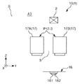
以下、図1〜図28および図60〜図63を参照して、本発明の電子部品搬送装置および電子部品検査装置の第1実施形態について説明する。なお、以下では、説明の便宜上、図1に示すように、互いに直交する3軸をX軸、Y軸およびZ軸とする。また、X軸とY軸を含むXY平面が水平となっており、Z軸が鉛直となっている。また、X軸に平行な方向を「X方向(第3方向)」とも言い、Y軸に平行な方向を「Y方向(第2方向)」とも言い、Z軸に平行な方向を「Z方向(第1方向)」とも言う。また、各方向の矢印が向いた方向を「正(+)」、その反対方向を「負(−)」と言う。また、本願明細書で言う「水平」とは、完全な水平に限定されず、電子部品の搬送が阻害されない限り、水平に対して若干(例えば5°未満程度)傾いた状態も含む。また、図1、図4〜図11、図16〜図20、図23および図60中の上側を「上」または「上方」、下側を「下」または「下方」と言うことがある。特に、第1方向および第2方向が互いに直交していることにより、電子部品搬送装置10の各部を作動させる制御動作を簡単に行うことができる。
<First Embodiment>
Hereinafter, with reference to FIGS. 1-28 and FIGS. 60-63, 1st Embodiment of the electronic component conveying apparatus and electronic component inspection apparatus of this invention is described. In the following, for convenience of explanation, as shown in FIG. 1, three axes orthogonal to each other are referred to as an X axis, a Y axis, and a Z axis. Further, the XY plane including the X axis and the Y axis is horizontal, and the Z axis is vertical. A direction parallel to the X axis is also referred to as “X direction (third direction)”, a direction parallel to the Y axis is also referred to as “Y direction (second direction)”, and a direction parallel to the Z axis is referred to as “Z direction”. (First direction) ". The direction in which the arrow in each direction is directed is called “positive (+)”, and the opposite direction is called “negative (−)”. In addition, the term “horizontal” in the specification of the present application is not limited to complete horizontal, and includes a state slightly inclined (for example, less than about 5 °) with respect to the horizontal as long as transportation of electronic components is not hindered. In addition, the upper side in FIGS. 1, 4 to 11, 16 to 20, 23, and 60 may be referred to as “upper” or “upper”, and the lower side may be referred to as “lower” or “lower”. In particular, since the first direction and the second direction are orthogonal to each other, a control operation for operating each part of the electronic
なお、図16〜図19では、検査部の大きさを誇張して図示しており、実際の寸法とは、大きく異なる。 16 to 19, the size of the inspection portion is exaggerated and is greatly different from the actual size.
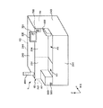
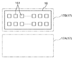
本発明の電子部品搬送装置10は、電子部品を載置する凹部161(載置部)を有する検査部16(電子部品載置部)を配置可能で、Z方向(第1方向)と、Z方向と異なるY方向(第2方向)とに移動可能であり、電子部品を把持可能な第1把持部としてのデバイス搬送ヘッド17Aと、Z方向およびY方向に移動可能であり、電子部品を把持可能な第2把持部としてのデバイス搬送ヘッド17Bと、デバイス搬送ヘッド17Aおよびデバイス搬送ヘッド17Bの間から検査部16(電子部品載置部)を撮像可能な撮像部としての第1カメラ31および第2カメラ32と、デバイス搬送ヘッド17Aおよびデバイス搬送ヘッド17Bのうちの少なくとも1つのデバイス搬送ヘッド(把持部)の位置情報を検出可能な位置検出部としてのエンコーダー23と、を有し、デバイス搬送ヘッド17Aおよびデバイス搬送ヘッド17Bは、撮像部としての第1カメラ31および第2カメラ32に対して第2方向に移動可能で、撮像部としての第1カメラ31および第2カメラ32は、エンコーダー23が検出した第1位置情報(エンコーダー値)に基づいて検査部16の第1像を撮像する。
The electronic
これにより、デバイス搬送ヘッド17Aまたはデバイス搬送ヘッド17Bの位置情報に基づいて撮像を行うことができる。よって、デバイス搬送ヘッド17Aおよびデバイス搬送ヘッド17Bの間から電子部品載置部を撮像することができる。その結果、例えば、撮像結果に基づいて、載置部に電子部品が配置されているか否かを判断する場合、その判断をより正確に行うことができる。
Thereby, imaging can be performed based on the position information of the
本発明の電子部品検査装置1は、電子部品を載置する凹部161(載置部)を有する検査部16(電子部品載置部)を配置可能で、Z方向(第1方向)と、Z方向と異なるY方向(第2方向)とに移動可能であり、電子部品を把持可能な第1把持部としてのデバイス搬送ヘッド17Aと、Z方向およびY方向に移動可能であり、電子部品を把持可能な第2把持部としてのデバイス搬送ヘッド17Bと、デバイス搬送ヘッド17Aおよびデバイス搬送ヘッド17Bの間から検査部16(電子部品載置部)を撮像可能な撮像部としての第1カメラ31および第2カメラ32と、デバイス搬送ヘッド17Aおよびデバイス搬送ヘッド17Bのうちの少なくとも1つのデバイス搬送ヘッド(把持部)の位置情報を検出可能な位置検出部としてのエンコーダー23と、電子部品を検査する検査部16を有し、デバイス搬送ヘッド17Aおよびデバイス搬送ヘッド17Bは、撮像部としての第1カメラ31および第2カメラ32に対して第2方向に移動可能で、撮像部としての第1カメラ31および第2カメラ32は、エンコーダー23が検出した第1位置情報(エンコーダー値)に基づいて検査部16の第1像を撮像する。
The electronic
これにより、前述した電子部品搬送装置10の利点を持つ電子部品検査装置1が得られる。また、検査部16にまで電子部品を搬送することができ、よって、当該電子部品に対する検査を検査部16で行なうことができる。また、検査後の電子部品を検査部16から搬送することができる。
Thereby, the electronic
なお、本明細書中では、第2輝度は、第1輝度よりも小さければよく、ゼロの状態、すなわち、光照射部が光を照射していない状態も含む。 In the present specification, the second luminance only needs to be smaller than the first luminance, and includes a zero state, that is, a state where the light irradiation unit is not irradiating light.
以下、各部の構成について説明する。
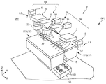
図1、図2に示すように、電子部品搬送装置10を内蔵する電子部品検査装置1は、例えばBGA(Ball Grid Array)パッケージであるICデバイス等の電子部品を搬送し、その搬送過程で電子部品の電気的特性を検査・試験(以下単に「検査」と言う)する装置である。なお、以下では、説明の便宜上、前記電子部品としてICデバイスを用いる場合について代表して説明し、これを「ICデバイス90」とする。ICデバイス90は、本実施形態では平板状をなすものとなっている。
Hereinafter, the configuration of each unit will be described.
As shown in FIGS. 1 and 2, an electronic
なお、ICデバイスとしては、前記のものの他に、例えば、「LSI(Large Scale Integration)」「CMOS(Complementary MOS)」「CCD(Charge Coupled Device)」や、ICデバイスを複数モジュールパッケージ化した「モジュールIC」、また、「水晶デバイス」、「圧力センサー」、「慣性センサー(加速度センサー)」、「ジャイロセンサー」、「指紋センサー」等が挙げられる。 In addition to the above-mentioned IC devices, for example, “LSI (Large Scale Integration)”, “CMOS (Complementary MOS)”, “CCD (Charge Coupled Device)”, or “modules” in which a plurality of IC devices are packaged. IC "," quartz device "," pressure sensor "," inertial sensor (acceleration sensor) "," gyro sensor "," fingerprint sensor ", and the like.
また、電子部品検査装置1(電子部品搬送装置10)は、ICデバイス90の種類ごとに交換される「チェンジキット」と呼ばれるものを予め搭載して用いられる。このチェンジキットには、ICデバイス90が載置される載置部があり、その載置部としては、例えば、後述する温度調整部12、デバイス供給部14等がある。また、ICデバイス90が載置される載置部としては、前記のようなチェンジキットとは別に、ユーザーが用意する検査部16やトレイ200もある。
Also, the electronic component inspection apparatus 1 (electronic component transport apparatus 10) is used by mounting in advance a so-called “change kit” that is exchanged for each type of
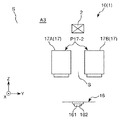
電子部品検査装置1は、トレイ供給領域A1と、デバイス供給領域(以下単に「供給領域」と言う)A2と、検査領域A3と、デバイス回収領域(以下単に「回収領域」と言う)A4と、トレイ除去領域A5とを備え、これらの領域は、後述するように各壁部で分けられている。そして、ICデバイス90は、トレイ供給領域A1からトレイ除去領域A5まで前記各領域を矢印α90方向に順に経由し、途中の検査領域A3で検査が行われる。このように電子部品検査装置1は、各領域でICデバイス90を搬送する電子部品搬送装置10であるハンドラーと、検査領域A3内で検査を行なう検査部16と、制御部800とを備えたものとなっている。また、その他、電子部品検査装置1は、モニター300と、シグナルランプ400と、操作パネル700とを備えている。
The electronic
なお、電子部品検査装置1は、トレイ供給領域A1、トレイ除去領域A5が配された方、すなわち、図2中の下側が正面側となり、検査領域A3が配された方、すなわち、図2中の上側が背面側として使用される。
In the electronic
トレイ供給領域A1は、未検査状態の複数のICデバイス90が配列されたトレイ200が供給される給材部である。トレイ供給領域A1では、多数のトレイ200を積み重ねることができる。
The tray supply area A1 is a material supply unit to which a
供給領域A2は、トレイ供給領域A1から搬送されたトレイ200上の複数のICデバイス90がそれぞれ検査領域A3まで搬送、供給される領域である。なお、トレイ供給領域A1と供給領域A2とを跨ぐように、トレイ200を1枚ずつ水平方向に搬送するトレイ搬送機構11A、11Bが設けられている。トレイ搬送機構11Aは、トレイ200を、当該トレイ200に載置されたICデバイス90ごとY方向の正側、すなわち、図2中の矢印α11A方向に移動させることができる移動部である。これにより、ICデバイス90を安定して供給領域A2に送り込むことができる。また、トレイ搬送機構11Bは、空のトレイ200をY方向の負側、すなわち、図2中の矢印α11B方向に移動させることができる移動部である。これにより、空のトレイ200を供給領域A2からトレイ供給領域A1に移動させることができる。
The supply area A2 is an area where a plurality of
供給領域A2には、温度調整部(ソークプレート(英語表記:soak plate、中国語表記(一例):均温板))12と、デバイス搬送ヘッド13と、トレイ搬送機構15とが設けられている。
In the supply area A2, a temperature adjustment unit (soak plate (English notation: soak plate, Chinese notation (example): soaking plate)) 12, a
温度調整部12は、複数のICデバイス90が載置される載置部として構成され、当該載置されたICデバイス90を一括して加熱または冷却することができる「ソークプレート」と呼ばれる。このソークプレートにより、検査部16で検査される前のICデバイス90を予め加熱または冷却して、当該検査(高温検査または低温検査)に適した温度に調整することができる。図2に示す構成では、温度調整部12は、Y方向に2つ配置、固定されている。そして、トレイ搬送機構11Aによってトレイ供給領域A1から搬入されたトレイ200上のICデバイス90は、いずれかの温度調整部12まで搬送される。なお、この載置部としての温度調整部12は、固定されていることにより、当該温度調整部12上でのICデバイス90に対して安定して温度調整することができる。
The
デバイス搬送ヘッド13は、供給領域A2内でX方向およびY方向に移動可能に支持され、さらにZ方向にも移動可能な部分を有している。これにより、デバイス搬送ヘッド13は、トレイ供給領域A1から搬入されたトレイ200と温度調整部12との間のICデバイス90の搬送と、温度調整部12と後述するデバイス供給部14との間のICデバイス90の搬送とを担うことができる。なお、図2中では、デバイス搬送ヘッド13のX方向の移動を矢印α13Xで示し、デバイス搬送ヘッド13のY方向の移動を矢印α13Yで示している。
The
トレイ搬送機構15は、全てのICデバイス90が除去された状態の空のトレイ200を供給領域A2内でX方向の正側、すなわち、矢印α15方向に搬送する機構である。そして、この搬送後、空のトレイ200は、トレイ搬送機構11Bによって供給領域A2からトレイ供給領域A1に戻される。
検査領域A3は、ICデバイス90を検査する領域である。この検査領域A3には、ICデバイス90に対して検査を行なう検査部16と、デバイス搬送ヘッド17とが設けられている。また、供給領域A2と検査領域A3とを跨ぐように移動するデバイス供給部14と、検査領域A3と回収領域A4とを跨ぐように移動するデバイス回収部18も設けられている。
The inspection area A3 is an area where the
デバイス供給部14は、温度調整部12で温度調整されたICデバイス90が載置される載置部として構成され、当該ICデバイス90を検査部16近傍まで搬送することができる「供給用シャトルプレート」または単に「供給シャトル」と呼ばれるものである。
The
また、この載置部としてのデバイス供給部14は、供給領域A2と検査領域A3との間をX方向、すなわち、矢印α14方向に沿って往復移動可能に支持されている。これにより、デバイス供給部14は、ICデバイス90を供給領域A2から検査領域A3の検査部16近傍まで安定して搬送することができ、また、検査領域A3でICデバイス90がデバイス搬送ヘッド17によって取り去られた後は再度供給領域A2に戻ることができる。
The
図2に示す構成では、デバイス供給部14は、Y方向に2つ配置されており、温度調整部12上のICデバイス90は、いずれかのデバイス供給部14まで搬送される。また、デバイス供給部14は、温度調整部12と同様に、当該デバイス供給部14に載置されたICデバイス90を加熱または冷却可能に構成されている。これにより、温度調整部12で温度調整されたICデバイス90に対して、その温度調整状態を維持して、検査領域A3の検査部16近傍まで搬送することができる。
In the configuration shown in FIG. 2, two
デバイス搬送ヘッド17は、前記温度調整状態が維持されたICデバイス90が把持され、当該ICデバイス90を検査領域A3内で搬送する動作部である。このデバイス搬送ヘッド17は、検査領域A3内でY方向およびZ方向に往復移動可能に支持され、「インデックスアーム」と呼ばれる機構の一部となっている。これにより、デバイス搬送ヘッド17は、供給領域A2から搬入されたデバイス供給部14上のICデバイス90を検査部16上に搬送し、載置することができる。なお、図2中では、デバイス搬送ヘッド17のY方向の往復移動を矢印α17Yで示している。また、デバイス搬送ヘッド17は、Y方向に往復移動可能に支持されているが、これに限定されず、X方向にも往復移動可能に支持されていてもよい。
The
また、デバイス搬送ヘッド17は、第1方向であるZ方向と、Z方向と異なる第2方向であるY方向とに移動可能であり、ICデバイス90を把持可能な第1把持部としてのデバイス搬送ヘッド17Aと、デバイス搬送ヘッド17Aとは独立してY方向およびZ方向に移動可能であり、ICデバイス90を把持可能な第2把持部であるデバイス搬送ヘッド17Bと、を有する。特に、図18および図19に示すように、デバイス搬送ヘッド17Aおよびデバイス搬送ヘッド17Bが互いに独立してZ方向に移動する構成とすることにより、デバイス搬送ヘッド17Aおよびデバイス搬送ヘッド17Bの双方が下降して、後述する第1カメラ31および第2カメラ32の撮像可能エリアが小さくなるのを防止することができる。
In addition, the
第1把持部としてのデバイス搬送ヘッド17Aと第2把持部としてのデバイス搬送ヘッド17Bとは、第2方向であるY方向に並んで互いに離間して配置されている。また、これにより、例えば、検査部16よりも−Y側のデバイス供給部14またはデバイス回収部18と検査部16との間でのICデバイス90の搬送をデバイス搬送ヘッド17Aが担い、検査部16よりも+Y側のデバイス供給部14またはデバイス回収部18と検査部16との間でのICデバイス90の搬送をデバイス搬送ヘッド17Bが担う構成とすることができる。よって、デバイス搬送ヘッド17全体で見たときの移動距離を低減することができ、搬送効率に優れる。
The
また、第1把持部としてのデバイス搬送ヘッド17Aと第2把持部としてのデバイス搬送ヘッド17Bとは、第2方向であるY方向に同時に移動可能である。これにより、例えば、デバイス搬送ヘッド17AがICデバイス90を押圧しているときに、デバイス搬送ヘッド17Bが異なる動作(デバイス供給部14またはデバイス回収部18との間でのICデバイス90のやり取り等)を行うことができたり、その逆も行うことができる。よって、搬送効率や検査効率を高めることができる。
Further, the
また、図1に示すように、電子部品搬送装置10は、第1把持部としてのデバイス搬送ヘッド17A、または、第2把持部としてのデバイス搬送ヘッド17Bの位置を検出する位置検出部としてのエンコーダー23を有する。本実施形態では、エンコーダー23は、デバイス搬送ヘッド17Aおよびデバイス搬送ヘッド17BのそれぞれのY方向およびZ方向の位置を検出する。これにより、後述するように、例えば、第1カメラ31および第2カメラ32が検査部16を撮像可能なときの、デバイス搬送ヘッド17Aおよびデバイス搬送ヘッド17Bの位置を検出することができる。このエンコーダー23は、図3に示すように、制御部800と電気的に接続され、デバイス搬送ヘッド17Aおよびデバイス搬送ヘッド17Bの位置情報が、制御部800に送信される。
Further, as shown in FIG. 1, the electronic
このようなデバイス搬送ヘッド17は、温度調整部12と同様に、把持したICデバイス90を加熱または冷却可能に構成されている。これにより、ICデバイス90における温度調整状態を、デバイス供給部14から検査部16まで継続して維持することができる。
Similar to the
検査部16は、電子部品であるICデバイス90を載置して、当該ICデバイス90の電気的特性を検査する電子部品載置部である。この検査部16は、Z方向から見たとき、X方向に延在する長方形の板状をなしている。また、検査部16は、ICデバイス90を収納する複数(本実施形態では、16個)の凹部161を有している。各凹部は、X方向に8個並んで設けられ、この8個の列がY方向に2列設けられた格子状に配置されている。また、図11に示すように、各凹部161は、その内周面がテーパ状をなしている。すなわち、各凹部161は、第3方向であるX方向に対して傾斜する内周面162を有している。
The
また、凹部161の底部には、ICデバイス90の端子(図示せず)と電気的に接続される複数のプローブピン(図示せず)が設けられている。そして、ICデバイス90の端とプローブピンとが電気的に接続される、すなわち、接触することにより、ICデバイス90の検査を行なうことができる。ICデバイス90の検査は、検査部16に接続されるテスターが備える検査制御部に記憶されているプログラムに基づいて行われる。なお、検査部16でも、温度調整部12と同様に、ICデバイス90を加熱または冷却して、当該ICデバイス90を検査に適した温度に調整することができる。
A plurality of probe pins (not shown) that are electrically connected to terminals (not shown) of the
デバイス回収部18は、検査部16で検査が終了したICデバイス90が載置され、当該ICデバイス90を回収領域A4まで搬送することができる載置部として構成され、「回収用シャトルプレート」または単に「回収シャトル」と呼ばれる。
The
また、デバイス回収部18は、検査領域A3と回収領域A4との間をX方向、すなわち、矢印α18方向に沿って往復移動可能に支持されている。また、図2に示す構成では、デバイス回収部18は、デバイス供給部14と同様に、Y方向に2つ配置されており、検査部16上のICデバイス90は、いずれかのデバイス回収部18に搬送され、載置される。この搬送は、デバイス搬送ヘッド17によって行なわれる。
The
回収領域A4は、検査領域A3で検査され、その検査が終了した複数のICデバイス90が回収される領域である。この回収領域A4には、回収用トレイ19と、デバイス搬送ヘッド20と、トレイ搬送機構21とが設けられている。また、回収領域A4には、空のトレイ200も用意されている。
The collection area A4 is an area in which a plurality of
回収用トレイ19は、検査部16で検査されたICデバイス90が載置される載置部であり、回収領域A4内で移動しないよう固定されている。これにより、デバイス搬送ヘッド20等の各種可動部が比較的多く配置された回収領域A4であっても、回収用トレイ19上では、検査済みのICデバイス90が安定して載置されることとなる。なお、図2に示す構成では、回収用トレイ19は、X方向に沿って3つ配置されている。
The
また、空のトレイ200も、X方向に沿って3つ配置されている。この空のトレイ200も、検査部16で検査されたICデバイス90が載置される載置部となる。そして、回収領域A4に移動してきたデバイス回収部18上のICデバイス90は、回収用トレイ19および空のトレイ200のうちのいずれかに搬送され、載置される。これにより、ICデバイス90は、検査結果ごとに分類されて、回収されることとなる。
Three
デバイス搬送ヘッド20は、回収領域A4内でX方向およびY方向に移動可能に支持され、さらにZ方向にも移動可能な部分を有している。これにより、デバイス搬送ヘッド20は、ICデバイス90をデバイス回収部18から回収用トレイ19や空のトレイ200に搬送することができる。なお、図2中では、デバイス搬送ヘッド20のX方向の移動を矢印α20Xで示し、デバイス搬送ヘッド20のY方向の移動を矢印α20Yで示している。
The
トレイ搬送機構21は、トレイ除去領域A5から搬入された空のトレイ200を回収領域A4内でX方向、すなわち、矢印α21方向に搬送する機構である。そして、この搬送後、空のトレイ200は、ICデバイス90が回収される位置に配されることとなる、すなわち、前記3つの空のトレイ200のうちのいずれかとなり得る。
トレイ除去領域A5は、検査済み状態の複数のICデバイス90が配列されたトレイ200が回収され、除去される除材部である。トレイ除去領域A5では、多数のトレイ200を積み重ねることができる。
The tray removal area A5 is a material removal unit from which the
また、回収領域A4とトレイ除去領域A5とを跨ぐように、トレイ200を1枚ずつY方向に搬送するトレイ搬送機構22A、22Bが設けられている。トレイ搬送機構22Aは、トレイ200をY方向、すなわち、矢印α22A方向に往復移動させることができる移動部である。これにより、検査済みのICデバイス90を回収領域A4からトレイ除去領域A5に搬送することができる。また、トレイ搬送機構22Bは、ICデバイス90を回収するための空のトレイ200をY方向の正側、すなわち、矢印α22B方向に移動させることができる。これにより、空のトレイ200をトレイ除去領域A5から回収領域A4に移動させることができる。
In addition,
制御部800は、例えば、トレイ搬送機構11Aと、トレイ搬送機構11Bと、温度調整部12と、デバイス搬送ヘッド13と、デバイス供給部14と、トレイ搬送機構15と、検査部16と、デバイス搬送ヘッド17と、デバイス回収部18と、デバイス搬送ヘッド20と、トレイ搬送機構21と、トレイ搬送機構22Aと、トレイ搬送機構22Bの各部の作動を制御することができる。
For example, the
また、図3に示すように、制御部800は、メモリー802(記憶部)を有している。メモリー802は、例えば不揮発性半導体メモリーの一種であるEEPROM(Electrically Erasable Programmable Read-Only Memory)等を有し、上記検査等の各種プログラム等が記憶されている。
As shown in FIG. 3, the
また、図3に示すように、制御部800は、後述する光照射部であるレーザー光源41がレーザー光Lを照射する方向が、予め定められた方向か否かの判断する照射位置判断部801を有する。これにより、例えば、レーザー光源41がレーザー光Lを照射する方向が所望の方向か否かを判断することができる。
As shown in FIG. 3, the
また、制御部800は、後述するように、撮像部としての第1カメラ31および第2カメラ32に対して撮像指令信号を送信するタイミングを調整可能である。これにより、撮像部が撮像した画像において、載置部が映るよう調整することができる。特に、制御部800は、後述するように、撮像部としての第1カメラ31および第2カメラ32が撮像を開始するタイミングを調整可能であるため、撮像指令信号を送信するタイミングの調整を正確に行うことができる。
Moreover, the
オペレーターは、モニター300を介して、電子部品検査装置1の動作条件等を設定したり、確認したりすることができる。このモニター300は、例えば液晶画面で構成された表示画面301を有し、電子部品検査装置1の正面側上部に配置されている。図1に示すように、トレイ除去領域A5の図中の右側には、マウスを載置するマウス台600が設けられている。このマウスは、モニター300に表示された画面を操作する際に用いられる。
The operator can set or confirm the operating conditions of the electronic
また、モニター300に対して図1の右下方には、操作パネル700が配置されている。操作パネル700は、モニター300とは別に、電子部品検査装置1に所望の動作を命令するものである。
In addition, an
また、シグナルランプ400は、発光する色の組み合わせにより、電子部品検査装置1の作動状態等を報知することができる。シグナルランプ400は、電子部品検査装置1の上部に配置されている。なお、電子部品検査装置1には、スピーカー500が内蔵されており、このスピーカー500によっても電子部品検査装置1の作動状態等を報知することもできる。
Further, the
これら、モニター300およびスピーカー500は、後述するように、検査部16の凹部161にICデバイス90が配置されているか否かの判断の結果を報知する報知部24として機能する。これにより、電子部品搬送装置10のオペレーターに判断の結果を知らせることができる。
As will be described later, the
電子部品検査装置1は、トレイ供給領域A1と供給領域A2との間が第1隔壁231によって区切られており、供給領域A2と検査領域A3との間が第2隔壁232によって区切られており、検査領域A3と回収領域A4との間が第3隔壁233によって区切られており、回収領域A4とトレイ除去領域A5との間が第4隔壁234によって区切られている。また、供給領域A2と回収領域A4との間も、第5隔壁235によって区切られている。
In the electronic
電子部品検査装置1は、最外装がカバーで覆われており、当該カバーには、例えばフロントカバー241、サイドカバー242、サイドカバー243、リアカバー244、トップカバー245がある。
The outermost exterior of the electronic
次に、検出ユニット2について説明する。
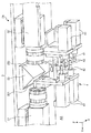
図4および図5に示すように、検出ユニット2は、検出ユニット2Aと、検出ユニット2Bとを有している。検出ユニット2Aおよび検出ユニット2Bは、デバイス搬送ヘッド17の+Z側に設けられ(図5参照)、この順で+X方向から並んで配置されている。
Next, the
As shown in FIGS. 4 and 5, the
検出ユニット2Aおよび検出ユニット2Bは、それぞれ、撮像ユニット3と、光照射ユニット4と、照明5とを有している。検出ユニット2Aおよび検出ユニット2Bは、撮像ユニット3と、光照射ユニット4と、照明5との配置位置がY軸に対して線対称であること以外は、同じ構成であるため、以下、検出ユニット2Aについて代表的に説明する。
Each of the
図6および図7に示すように、撮像ユニット3は、第1カメラ31(第1撮像部)と、第2カメラ32(第2撮像部)と、光反射部33とを有している。
As shown in FIGS. 6 and 7, the
第1カメラ31は、例えば、CCD(Charge Coupled Device)カメラを用いることができる。また、第1カメラ31は、−Y方向を向いて配置されており、−Y側を撮像する。この第1カメラ31は、図3に示すように、制御部800と電気的に接続されており、その作動が制御される。
As the
第2カメラ32は、第1カメラ31と同様の構成とすることができる。また、第2カメラ32は、+Y方向を向いて配置されており、+Y側を撮像する。この第2カメラ32は、図3に示すように、制御部800と電気的に接続されており、その作動が制御される。
The
また、撮像部としての第1カメラ31および第2カメラ32は、撮像素子を有し、例えば、シャッター速度等を調整することにより、撮像素子の露光時間を調整可能である。これにより、撮像した画像の明るさを調整することができる。なお、露光時間の調整は、デバイス搬送ヘッド17Aおよびデバイス搬送ヘッド17Bの間から凹部161の全部を撮像可能なときに行われる。
In addition, the
光反射部33は、第1カメラ31と第2カメラ32との間に設けられている。この光反射部33は、検査部16の像を第1カメラ31および第2カメラ32に向って反射させるものである。
The
光反射部33は、光を反射する第1光反射面331(第1光反射部)と、光を反射する第2光反射面332(第2光反射部)とを有する。この光反射部33は、X方向から見たときに二等辺三角形(本実施形態では、直角二等辺三角形)の三角柱の部材であり、頂角が−Z側に位置するよう配置されている。
The
また、光反射部33では、+Y側の面が第1光反射面331として機能し、−Y側の面が第2光反射面332として機能する。
In the
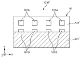
第1光反射面331は、第1カメラ31(第1撮像部)と第2カメラ32(第2撮像部)との間に設けられ、検査部16(電子部品載置部)の像を第1カメラ31に向って反射させるものである。第1光反射面331は、デバイス搬送ヘッド17A(第1把持部)とデバイス搬送ヘッド17B(第2把持部)との間から、第1カメラ31が、検査部16の像を撮像可能とする。第2光反射面332は、第2カメラ32(第2撮像部)と第1光反射面331との間に設けられ、検査部16(電子部品載置部)の像を第2カメラ32に向って反射させるものである。第2光反射面332は、デバイス搬送ヘッド17A(第1把持部)とデバイス搬送ヘッド17B(第2把持部)との間から、第2カメラ32が、検査部16の像を撮像可能とする。これにより、デバイス搬送ヘッド17Aとデバイス搬送ヘッド17Bとの間隙Sが比較的狭くても、第1カメラ31および第2カメラ32は、それぞれ、検査部16を撮像することができる。なお、本明細書における第1カメラ31および第2カメラ32の撮像方向は、Z方向とする。
The first
また、図20に示すように、第1カメラ31(第1撮像部)の第1光反射面331(第1光反射部)までの光軸と、第2カメラ32(第2撮像部)の光軸とは、Y方向(第2方向)に沿っている。すなわち、第1カメラ31(第1撮像部)の第1光反射面331(第1光反射部)までの光軸と、第2カメラ32(第2撮像部)の光軸とは、平行である。これにより、第1カメラ31、第2カメラ32および光反射部33の設置を容易に行うことができる。
As shown in FIG. 20, the optical axis to the first light reflecting surface 331 (first light reflecting portion) of the first camera 31 (first imaging portion) and the second camera 32 (second imaging portion). The optical axis is along the Y direction (second direction). That is, the optical axis to the first light reflecting surface 331 (first light reflecting unit) of the first camera 31 (first imaging unit) and the optical axis of the second camera 32 (second imaging unit) are parallel. is there. Thereby, installation of the
第1カメラ31(第1撮像部)と第2カメラ32(第2撮像部)とは、光が入射する方向が互いに反対方向である。すなわち、第1カメラ31と第2カメラ32とは、互いに向かい合って反対方向を撮像する配置である。これにより、デバイス搬送ヘッド17Aとデバイス搬送ヘッド17Bとの間隙Sが比較的狭くても、第1カメラ31と第2カメラ32との間に光反射部33を設けることにより、第1カメラ31と第2カメラ32とは、それぞれ、検査部16を撮像することができる。
In the first camera 31 (first imaging unit) and the second camera 32 (second imaging unit), the light incident directions are opposite to each other. In other words, the
このような構成とすることにより、第1カメラ31(第1撮像部)および第2カメラ32(第2撮像部)は、検査部16(電子部品載置部)において、互いに位置が異なる領域を撮像することができる。よって、検査部16のより多くの領域を撮像することができる。
By adopting such a configuration, the first camera 31 (first imaging unit) and the second camera 32 (second imaging unit) have regions whose positions are different from each other in the inspection unit 16 (electronic component placement unit). An image can be taken. Therefore, a larger area of the
また、図7に示すように、第1撮像部である第1カメラ31は、その光軸O32が、後述する各光反射部であるミラー42が並んでいる方向(X方向)の延長線L42と交わるよう配置されている。これにより、第1カメラ31は、各ミラー42で反射したレーザー光L1が検査部16に照射された部分を撮像することができる。
As shown in FIG. 7, the
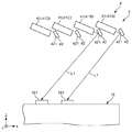
光照射ユニット4は、4つのレーザー光源(光照射部)41と、各レーザー光源41に対応して設けられ、レーザー光源41から出射されたレーザー光L1を反射する4つのミラー42と、各ミラー42を回動させる4つのモーター43とを有している。すなわち、光照射ユニット4では、光照射部であるレーザー光源41および光反射部であるミラー42は、複数(4つ)ずつ設けられている。
The
レーザー光源41(光照射部)は、デバイス搬送ヘッド17A(第1把持部)とデバイス搬送ヘッド17B(第2把持部)との間を通して、電子部品載置部である検査部16にレーザー光L1(光)を照射可能に配置されている。これにより、検査部16に照射されたレーザー光L1に基づいて、後述する判断を行うことができる。
The laser light source 41 (light irradiation unit) passes between the
レーザー光源41としては、公知のレーザー光源を用いることができ、出射するレーザー光L1の色は、特に限定されない。また、光照射部としてのレーザー光源41は、照射先(検査部16または検査部16上のICデバイス90)での照射形状が、Y方向(第2方向)の延在する線状のレーザー光L1(光)を照射するものである。これにより、後述するように、第1カメラ31および第2カメラ32が撮像した画像において、ICデバイス90の有無に応じて、照射されたレーザー光L1の位置の変化を分かり易くすることができる。よって、ICデバイス90が検査部16に残留しているか否かをより正確に検出することができる。
A known laser light source can be used as the
また、図4および図5に示すように、レーザー光源41が照射するレーザー光L1は、照射先の検査部16では、Y方向に並んだ2つの凹部161を包含するよう構成されている。すなわち、1つのレーザー光源41は、Y方向に並んだ2つの凹部161に一括してレーザー光L1を照射する。このようなレーザー光源41(光照射部)が、4つ(複数)設けられており、かつ、第3方向であるX方向に沿って並んで配置されていることにより、4つのレーザー光源41で8つの凹部161にレーザー光L1を照射することができる。そして、検出ユニット2Aおよび検出ユニット2Bで、合計8つのレーザー光源41が設けられていることにより、16個の凹部161の各々にレーザー光L1を照射することができる。
As shown in FIGS. 4 and 5, the laser light L <b> 1 irradiated by the
また、図8に示すように、Y方向から見たとき、各レーザー光源41は、X方向に対して傾斜して配置されている。このため、レーザー光源41が隣接するミラー42と干渉するのを防止することができる。その結果、レーザー光源41とミラー42とのX方向の距離を可及的に小さくすることができ、光照射ユニット4の小型化に寄与する。特に、電子部品搬送装置10では、デバイス搬送ヘッド17の+Z側のスペースは限られており、光照射ユニット4の小型化を図ることにより、電子部品搬送装置10全体の小型化に寄与する。
Moreover, as shown in FIG. 8, when viewed from the Y direction, each
このようなレーザー光源41は、制御部800と電気的に接続されており、その作動が制御される(図3参照)。
Such a
図6および図7に示すように、光照射ユニット4は、光照射部であるレーザー光源41が出射したレーザー光L1を反射する光反射部としてのミラー42を有する。これにより、レーザー光源41の向きを問わずレーザー光源41を配置することができる。よって、レーザー光源41の配置の自由度を高めることができる。
As shown in FIGS. 6 and 7, the
このミラー42は、図8に示すように、レーザー光L1を反射する反射面421を有しており、反射面421がレーザー光源41側に臨むように配置されている。
As shown in FIG. 8, the
また、各ミラー42は、Z方向(第1方向)およびY方向(第2方向)に対して交わるX方向(第3方向)に並んで配置されている。これにより、各レーザー光源41の配置形態に合わせることができるとともに、各ミラー42の配置形態を簡素にすることができる。
The
また、光照射ユニット4は、光反射部としてのミラー42を回動させる光反射部駆動部としての4つのモーター43を有している。ミラー42が、回動可能に構成されていることにより、ミラー42の反射面421の向きを調整することができ、レーザー光L1の照射位置を調整することができる。
Moreover, the
また、図9に示すように、ミラー42は、その回動軸Oが、前記光反射面上に位置するよう、モーター43に接続されている。これにより、ミラー42を回動させてレーザー光L1の照射方向を調整する際、その調整を正確に行うことができる。
Further, as shown in FIG. 9, the
このように、電子部品搬送装置10では、光照射部としてのレーザー光源41が照射するレーザー光L1の方向を調整可能であるため、レーザー光L1の検査部16での照射位置を調整したり、凹部161の配置箇所が図4および図5に示す構成とは異なる検査部にも対応することができる。
As described above, in the electronic
また、光照射部であるレーザー光源41が、少なくとも第1方向であるZ方向に対して傾斜した、すなわち、交差し、かつ、直交しない方向にレーザー光L1を照射するように調整することにより、後述するように、ICデバイス90の有無に応じて、照射されたレーザー光L1の位置の変化を分かり易くすることができる。
Further, by adjusting the
また、光反射部駆動部としての各モーター43は、第3方向であるX方向に沿って並んで配置されている。そして、X方向に隣り合うモーター43は、第2の方向であるY方向にずれて配置されており、いわゆる千鳥配置となっている。これにより、モーター43同士のX方向の間隔を比較的小さくしても、X方向に隣り合うモーター43同士が干渉し合うのを防止することができる。その結果、光照射ユニット4の小型化を図ることができる。
Moreover, each
照明5(第2光照射部)は、レーザー光L1よりも輝度が小さい光L2を照射するものである。また、光L2は、レーザー光L1よりも指向性が低く、検査部16全体を照らすよう構成されている。照明5は、光照射部であるレーザー光源41よりも輝度が小さい光L2を出射する第2光照射部である。これにより、レーザー光源41が照射する光に足りない照射条件(例えば、レーザー光L1よりも低い指向性)の光L2を照射することができる。また、照明5は、光照射ユニット4の+X側に配置されている。
The illumination 5 (second light irradiation unit) irradiates light L2 having a lower luminance than the laser light L1. The light L2 has a lower directivity than the laser light L1, and is configured to illuminate the
また、第2光照射部である照明5は、出射する光の輝度を調整可能であるこれにより、照明5が出射する光L2の照度を調整することができる。よって、後述する判断(第2判断)に際し、より良い条件の画像を用いることができる。
Moreover, the
このような検出ユニット2によれば、検査部16の凹部161におけるICデバイス90の有無を検出することができる。以下、この原理について、図10〜図13を用いて説明するが、各凹部161において同様の検出を行うため、1つの凹部161での検出について代表的に説明する。また、以下では、第1カメラ31が撮像した凹部161の画像のひとつを代表的に説明するが、第2カメラ32が撮像した凹部161の画像についても同様の制御を行うことができる。
According to such a
図10は、検出ユニット2を模式的に示した図であって、検出ユニット2をY方向から見た図である。また、図10では、レーザー光源41からレーザー光L1を検査部16に向って照射している。ICデバイス90が検査部16上に載置されていた場合(以下、この状態を「残留状態」と言う)には、レーザー光L1は、ICデバイス90上の位置P1に照射され、この位置P1には、照射形状が線状をなすレーザー光L1のラインが形成される。一方、ICデバイス90が検査部16上に無かった場合(以下、この状態を「除去状態」と言う)には、レーザー光L1は、検査部16の凹部161の底部の位置P2に照射され、この位置P2には、照射形状が線状をなすレーザー光L1のラインが形成される。なお、本明細書中での「線状」とは、1本の直線や、互いに離間して一方向に並んだ点の集合体や、楕円形や、長方形等、長尺な形状のもののことを言う。
FIG. 10 is a diagram schematically showing the
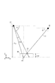
また、第1カメラ31は、残留状態および除去状態において、それぞれ画像(第1画像)を撮像する。図12には、残留状態で第1カメラ31が撮像した画像D1の一部を示しており、図13には、除去状態で第1カメラ31が撮像した画像D2の一部を示している。これら画像D1および画像D2は、撮像した画像のうち、必要な部分(凹部161が映っている部分)がトリミングされて用いられる。
The
図12に示すように、画像D1では、ICデバイス90上でのレーザー光L1のラインの位置P1は、検査部16の上面でのレーザー光L1のラインの位置Pよりも−X側(図中左右方向)にずれている。これは、ICデバイス90の上面が、検査部16の上面よりも低い、すなわち、−Z側に位置しているためである。なお、位置Pと位置P1とのX方向(図中左右方向)のずれ量を、ずれ量ΔD1とする。
As shown in FIG. 12, in the image D1, the position P1 of the line of the laser beam L1 on the
一方、図13に示すように、画像D2では、凹部161の底部上でのレーザー光L1のラインの位置P2は、検査部16の上面でのレーザー光L1のラインの位置Pよりも−X側にずれている。これは、凹部161の底部が、検査部16の上面よりも低い、すなわち、−Z側に位置しているためである。なお、位置Pと位置P2とのX方向(図中左右方向)のずれ量を、ずれ量ΔD2とする。
On the other hand, as shown in FIG. 13, in the image D <b> 2, the position P <b> 2 of the laser light L <b> 1 line on the bottom of the
また、ずれ量ΔD1は、ずれ量ΔD2よりも小さい。これは、ICデバイス90の上面が、凹部161の底部よりも+Z側に位置しているためである。電子部品搬送装置10では、例えば、画像D1および画像D2におけるずれ量が、ずれ量ΔD1であるかずれ量ΔD2であるかにより、残留状態か除去状態かを検出(判断)することができる。
Further, the deviation amount ΔD1 is smaller than the deviation amount ΔD2. This is because the upper surface of the
ここで、ICデバイス90の厚さΔdは、薄ければ薄いほど、ずれ量ΔD1およびずれ量ΔD2の差が小さくなり、ずれ量ΔD1であるかずれ量ΔD2であるかを判別しにくい。従って、比較的薄いICデバイス90において、残留状態か除去状態かを判断するには、比較的高い分解能を有する第1カメラ31を用いる必要がある。具体的には、図10中、位置P1と第1カメラ31の中心(光軸)とを結んだ線分と、位置P2と第1カメラ31の中心(光軸)とを結んだ線分とのなす角度Δαを認識可能な分解能を有する第1カメラ31を用いれば、残留状態か除去状態かを判断することができる。例えば、ICデバイス90の厚さΔdが分かっていたら、どの程度の角度Δαを認識可能なカメラを用いればよいか、また、第1カメラ31の分解能が分かっていたらどの程度の厚さΔdのICデバイス90において上記判断が可能かということを知るために、本発明者らは、以下の2つの式(1)および式(2)を導き出した。
Here, the thinner the thickness Δd of the
位置P2と第1カメラ31の中心(光軸)とを結んだ線分とX軸とのなす角度をαとし、レーザー光L1の光軸とX軸とのなす角度をβとし、第1カメラ31での光軸と凹部161の底部との離間距離をdcamとしたとき、ICデバイス90の厚さΔdは、式(1)で表すことができ、角度Δαは、式(2)で表すことができる。
The angle formed by the line connecting the position P2 and the center (optical axis) of the

例えば、角度Δαが分かっていたら、式(1)に代入することにより、上記判断が可能なICデバイス90の最小の厚さΔdを知ることができる。また、厚さΔdが分かっていたら式(2)に代入することにより、第1カメラ31に必要な分解能を知ることができる。
For example, if the angle Δα is known, the minimum thickness Δd of the
なお、厚さΔdが0.2mm以上のICデバイス90に対して前記判断を行うことが可能であるのが好ましく、0.1mm以上の電子部品に対して前記判断を行うことが可能であるのがより好ましい。これにより、比較的薄いICデバイス90であっても、検査部16にICデバイス90が残留しているか否かを検出することができる。なお、厚さΔdが薄すぎると、比較的高い分解能の第1カメラ31を用いる必要がありコストがかかる。
It is preferable that the determination can be made for an
なお、レーザー光L1の光軸とX軸とのなす角度βは、小さければ小さいほど、ずれ量ΔD1およびずれ量ΔD2が大きくなり、画像において、ずれ量ΔD1であるかずれ量ΔD2であるかを判別しやすくすることができる。角度βが小さすぎると、レーザー光L1は、凹部161内への入射が困難となる場合がある。
Note that the smaller the angle β between the optical axis of the laser beam L1 and the X-axis, the larger the shift amount ΔD1 and the shift amount ΔD2, and in the image whether the shift amount ΔD1 or the shift amount ΔD2. It can be made easy to distinguish. If the angle β is too small, the laser light L1 may be difficult to enter the
そこで、図11に示すように、光照射部であるレーザー光源41が出射するレーザー光L1の入射角θ1は、凹部161の内周面162とZ方向とのなす角度θ2よりも小さくするのが好ましい。これにより、凹部161内にレーザー光L1を照射することができる。その結果、ICデバイス90が凹部161内に残留しているか否かを検出することができる。
Therefore, as shown in FIG. 11, the incident angle θ1 of the laser light L1 emitted from the
以上、レーザー光L1を用いた判断(以下、この判断を「第1判断」とも言う)について説明した。電子部品搬送装置10は、第1判断とは異なる方式でも判断(以下、この判断を「第2判断」とも言う)を行うことができる。以下、このことについて図14および図15を用いて説明する。
The determination using the laser beam L1 (hereinafter, this determination is also referred to as “first determination”) has been described above. The electronic
図14および図15は、照明5によって検査部16に向って光L2を照射し、この状態で第1カメラ31を用いて検査部16を撮像した画像(第2画像)を示している。また、図14は残留状態での画像D1’の一部を示しており、図15は、除去状態での画像D2’の一部を示している。
14 and 15 show an image (second image) obtained by irradiating the
電子部品搬送装置10では、撮像した画像D1’および画像D2’に基づいて、ICデバイス90の色や、明るさを検出し、残留状態か除去状態かを検出(判断)することができる。
このように、電子部品搬送装置10は、第1判断と第2判断とを行うことができる。
The electronic
Thus, the electronic
さて、電子部品搬送装置10では、検出ユニット2を設置するスペースを確保するのが困難である。例えば、検査部16の近傍、すなわち、Z方向から見て、検査部16から外れた位置に検出ユニット2を配置したとしても、レーザー光L1や光L2の照射可能範囲が限られてきたり、第1カメラ31および第2カメラ32の撮像可能エリアが限られてきたりする。これらのことを鑑みると、検査部16の直上、すなわち、検査部16の+Z側に配置して撮像を行うのが好ましいが、検査部16+Z側には、デバイス搬送ヘッド17が設けられている。
Now, in the electronic
そこで、電子部品搬送装置10では、検出ユニット2を、デバイス搬送ヘッド17の+Z側に配置し、2つのデバイス搬送ヘッド17Aおよびデバイス搬送ヘッド17Bの間の間隙Sを介して検出を行う構成とした。すなわち、間隙Sを介して検査部16に向って、レーザー光L1および光L2のうちの少なくとも一方を照射し、間隙Sを介して、第1カメラ31および第2カメラ32を用いて画像を撮像し、第1判断および第2判断のうちの少なくとも一方を行う構成とした。これにより、上記構成であっても、残留状態か除去状態かを正確に検出(判断)することができる。
Therefore, in the electronic
また、間隙Sは、比較的狭いため、第1カメラ31および第2カメラ32で検査部16の全エリア、特に、検査部16のY方向の全域を撮像するのは困難な場合がある。そこで、図16に示すように、デバイス搬送ヘッド17の移動中において、16個の凹部161のうち、−Y側の8個の凹部161を撮像可能なときに撮像を行い、図17に示すように、+Y側の8個の凹部161を撮像可能なときに撮像を行う。これにより、検査部16のY方向の全域の撮像が困難であっても、複数の画像に基づいて、各凹部161の撮像を行うことができ、各凹部161において残留状態か除去状態かを検出(判断)することができる。なお、撮像可能な状態におけるデバイス搬送ヘッド17の位置は、エンコーダー23によって検出され、撮像可能なときのエンコーダー値がメモリー802に記憶されている。
In addition, since the gap S is relatively narrow, it may be difficult to image the entire area of the
なお、電子部品搬送装置10では、デバイス搬送ヘッド17A(第1把持部)が、ICデバイス90を検査部16(電子部品載置部)に対して押圧しているとき、デバイス搬送ヘッド17Aは、第1カメラ31(撮像部)とICデバイス90との間に位置している場合がある(図18参照)。この場合、デバイス搬送ヘッド17Aが遮って、−Y側の8個の凹部161の撮像が困難となる。一方、デバイス搬送ヘッド17B(第2把持部)が、ICデバイス90を検査部16(電子部品載置部)に対して押圧しているとき、デバイス搬送ヘッド17Bは、第1カメラ31(撮像部)とICデバイス90との間に位置している場合がある(図19参照)。この場合、デバイス搬送ヘッド17Bが遮って、+Y側の8個の凹部161の撮像が困難となる。この問題を利用すると、例えば、第1カメラ31が、ICデバイス90を撮像可能なときだけ撮像する構成とする場合には、撮影が困難なタイミングが分かっているため、どのタイミングで撮像を省略するかの設定を容易に行うことができる。その結果、無駄な画像を撮像するのを防止することができる。
In the electronic
また、第1カメラ31および第2カメラ32は、撮像開始時刻から撮像終了時刻の間、デバイス搬送ヘッド17A(第1把持部)とデバイス搬送ヘッド17B(第2把持部)の間を介して検査部16(電子部品載置部)を撮像可能である。すなわち、撮像部としての第1カメラ31および第2カメラ32は、検査部16がデバイス搬送ヘッド17Aまたはデバイス搬送ヘッド17Bに遮られている状態では、撮像するのを省略する。よって、無駄なく撮像を行うことができるとともに、無駄に画像データが増えるのを防止することができる。
Further, the
このように、第1カメラ31(第1撮像部)および第2カメラ32(第2撮像部)が撮像する画像D1、D2に基づいて、検査部16(電子部品載置部)にICデバイス90(電子部品)が配置されているか否かの判断を行うことが可能である。このため、ICデバイス90が不本意に凹部161内に残留しているのを検出することができる。
Thus, based on the images D1 and D2 captured by the first camera 31 (first imaging unit) and the second camera 32 (second imaging unit), the
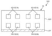
ここで、検査部16は、電子部品搬送装置10において、着脱可能に構成され、ICデバイス90の種類に応じて、最適なものに取り換えられて用いられることがある。このため、検査部16では、凹部161の配置位置や、配置個数が検査部16毎に異なる場合がある。以下、図20および図60に示すように、検査部16の凹部161がY方向に奇数列(図示の構成では、3列)設けられていた場合について説明する。なお、図20および図60は、検査部16を−X方向から見た図であり、これら図において、各凹部161を、+Y側から順に、凹部161A、凹部161Bおよび凹部161Cと言う。また、以下に述べることは、第1判断および第2判断の双方に適用可能であり、第1判断および第2判断を総称して「判断」とも言う。
Here, the
図60では、仮に、第1カメラ31および第2カメラ32を、第1カメラ31の光軸O31と第2カメラ32の光軸O32とが一致した状態で配置し、光反射部33を、第1カメラ31と第2カメラ32の中間に配置した場合を示している。
In FIG. 60, the
この場合、図61に示すように、第1カメラ31で撮像した画像D31’の図中上半分には、各凹部161Aの全域と、各凹部161Bの一部(半分)が映っている。また、画像31D’の図中下半分には、光反射部33よりも−Y側の像が映っている。この画像D31’では、図中上半分の領域が判断に用いられる使用領域A31’であり、図中下半分の領域が、判断の際に不要となる不要領域a31’である。
In this case, as shown in FIG. 61, in the upper half of the image D31 'captured by the
一方、図62に示すように、第2カメラ32で撮像した画像D32’の図中上半分には、光反射部33よりも+Y側の像が映っている。また、画像D32’の図中下半分には、凹部161Bの一部(半分)と、凹部161Cの全域とが映っている。この画像D32’では、図中上半分の領域が、判断の際に不要となる不要領域a32’であり、図中下半分の領域が判断に用いられる使用領域A32’である。
On the other hand, as shown in FIG. 62, an image on the + Y side of the
このような画像D31’および画像D32’に基づいて判断を行う場合、凹部161Aにおける判断は、画像D31’に基づいて行うことができる。また、凹部161Cにおける判断は、画像D32’に基づいて行うことができる。
When making a determination based on such an image D31 'and an image D32', the determination in the
そして、例えば、画像D31’および画像D32’を繋ぎ合わせ、凹部161Bを繋ぎ合わせた画像に基づいて、凹部161Bにおける判断を行うことができる。しかしながら、第1カメラ31および第2カメラ32の種類によっては、使用領域A31’と不要領域a32’との境界部で、ピントがぼけて不鮮明になる。すなわち、撮像した画像のうち、凹部161Bが映っている部分が不鮮明になる。この不鮮明な画像に基づいて凹部161Bの判断を行うと、その判断の信頼性が乏しくなる。そこで、電子部品搬送装置10では、この問題を以下の構成とすることにより、解消することができる。
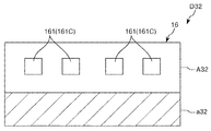
Then, for example, it is possible to make a determination in the
図20に示すように、電子部品搬送装置10では、光反射部33は、その頂点330が、検査部16のY方向の中心よりも−Y側にずれて配置されている。そして、さらに、第1カメラ31(第1撮像部)と、第2カメラ32(第2撮像部)とは、Z方向(第1方向)における位置が異なる。すなわち、第1カメラ31と第2カメラ32とは、設置高さ(鉛直方向での位置)が異なる。本実施形態では、第1カメラ31の方が第2カメラ32よりも高い位置、すなわち、+Z側に配置されている。このような構成により、第1カメラ31の第1光反射面331に対する高さと、第2カメラ32の第2光反射面332に対する高さとを異ならせることができる。よって、第1カメラ31が第1光反射面331を介して検査部16を撮像可能な領域と、第2カメラ32が第2光反射面332を介して検査部16を撮像可能な領域とで、検査部16における撮像位置を異ならせることができる。
As shown in FIG. 20, in the electronic
図21に示すように、第1カメラ31が撮像する画像D31には、凹部161Aおよび凹部161Bが映っている。なお、画像D31では、使用領域A31に凹部161Aおよび凹部161Bが映っており、画像D31の下側の不要領域a31には、凹部161Aおよび凹部161Bは映っていない。一方、第2カメラ32が撮像する画像D32には、凹部161Cが映っている。なお、画像D32では、使用領域A32に凹部161Cが映っており、画像D32の下側の不要領域a32には、凹部161Cは映っていない。
As shown in FIG. 21, the image D31 captured by the
このように、電子部品搬送装置10では、凹部161Aおよび凹部161Bの撮像を第1カメラ31が担い、凹部161Cの撮像を第2カメラ32が担っている。これにより、前述したような凹部161Bにおける画質の劣化を防止することができる。よって、凹部161Aおよび凹部161Cについてはもちろん、凹部161Bにおいても、ICデバイス90の有無の判断を正確に行うことができる。
As described above, in the electronic
このように、検査部16(電子部品載置部)における第1カメラ31(第1撮像部)が撮像する領域(第1撮像領域)と、検査部16(電子部品載置部)における第2カメラ32(第2撮像部)が撮像する領域(第2撮像領域)とは、大きさが異なる。すなわち、使用領域A31と使用領域A32との大きさが異なる。これにより、第1撮像領域と第2撮像領域との境界部の位置を検査部16のY方向の中心部からずらすことができる。よって、検査部16のY方向の中心部に位置する凹部161Bにおいても、ICデバイス90の有無の判断を正確に行うことができる。
As described above, the region (first imaging region) captured by the first camera 31 (first imaging unit) in the inspection unit 16 (electronic component placement unit) and the second in the inspection unit 16 (electronic component placement unit). The size is different from the region (second imaging region) captured by the camera 32 (second imaging unit). That is, the size of the use area A31 and the use area A32 is different. Thereby, the position of the boundary portion between the first imaging region and the second imaging region can be shifted from the central portion of the
また、第1カメラ31(第1撮像部)の、第1光反射面331(第1光反射部)から検査部16(電子部品載置部)までの光軸O31は、第2光反射面332(光反射部)を含む仮想平面と第2カメラ32(第2撮像部)の光軸O32との交点と交わっている。これにより、図20に示すように、第1カメラ31および第2カメラ32が撮像するアングルを、同じにすることができる。さらに、第1カメラ31および第2カメラ32が撮像するアングルを、理想の位置Pbestに撮像部を載置して撮像した場合のアングルと同じにすることができる。
The optical axis O31 from the first light reflecting surface 331 (first light reflecting portion) to the inspection unit 16 (electronic component placement portion) of the first camera 31 (first imaging unit) is the second light reflecting surface. It intersects with the intersection of the virtual plane including 332 (light reflecting section) and the optical axis O32 of the second camera 32 (second imaging section). Thereby, as shown in FIG. 20, the angle which the
なお、前述したように、デバイス搬送ヘッド17の+Z側のスペースは限られているため、理想の位置Pbestに撮像部を配置するのは困難である。しかしながら、第1カメラ31および第2カメラ32をY方向に沿って配置し、光反射部33を設けることにより、装置の小型化を図りつつ、検査部16の撮像を行うことができる。
As described above, since the space on the + Z side of the
なお、図20に示すように、第1光反射面331の法線N1と、第2光反射面332の法線N2とのなす角度θ3は、85°以上、95°以下であるのが好ましく、88°以上、92°以下であるのがより好ましい。これにより、光反射部33をX方向から見たときの頂角を略直角とすることができ、第1カメラ31および第2カメラ32を設置する際、第1カメラ31の光軸と第2カメラ32の光軸とを平行に設置すればよく、これらの設置を容易に行うことができる。
As shown in FIG. 20, the angle θ3 formed by the normal line N1 of the first
次に、ICデバイス90の検査を行うのに先立って行う、第1カメラ31および第2カメラ32が撮像を行うタイミングの調整方法(制御部800の制御動作)について説明するが、第1カメラ31および第2カメラ32では、同様の制御が行われるため、以下、第1カメラ31について代表的に説明する。
Next, a timing adjustment method (control operation of the control unit 800) at which the
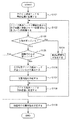
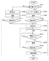
まず、ステップS101において、デバイス搬送ヘッド17Aおよびデバイス搬送ヘッド17Bを、開始位置Psに配置する(図23参照)。開始位置Psは、例えば、凹部161が見え始める位置である。
First, in step S101, the
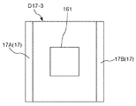
そして、ステップS102では、開始位置Psから終了位置Peに向ってデバイス搬送ヘッド17Aおよびデバイス搬送ヘッド17Bを移動させながら(図23中矢印α17Aおよび矢印α17B参照)、デバイス搬送ヘッド17Aおよびデバイス搬送ヘッド17Bのエンコーダー値が、予め決められた値となったときに、第1カメラ31に撮像指令信号を送信し、凹部161の撮像を1回行う。すなわち、エンコーダー23が検出した第1位置情報であるエンコーダー値に基づいて検査部16の像(第1像)を1回撮像し、図24に示す1つの画像D17−1を得る。
In step S102, the
なお、予め決められた値とは、デバイス搬送ヘッド17Aおよびデバイス搬送ヘッド17Bの間隙Sが凹部161と重なる位置のエンコーダー値を、凹部161の配置位置および位置検出部23の精度を考慮して理論的に推定して得られた値である。
The predetermined value is an encoder value at a position where the gap S between the
そして、ステップS103において、画像D17−1に凹部が映っているか否かを判断する。本ステップでは、凹部161の一部でも映っていた場合、ステップS105に移行する。図24に示すように、画像D17−1に、デバイス搬送ヘッド17Bが映っており、凹部161の全部を遮っていた場合には、凹部161が映っていないと判断し、ステップS104に移行する。
In step S103, it is determined whether or not a concave portion is reflected in the image D17-1. In this step, if even a part of the
そして、ステップS104において、画像D17−1を撮像した際に撮像指令信号を送信した時ときのエンコーダー値である第1位置情報を修正する。すなわち、第1カメラ31(撮像部)に撮像された第1像である画像D17−1に基づいて、次の補正した位置情報、すなわち、第1位置情報とは異なる第2位置情報を作成する。これにより、第1位置情報を踏まえてより正確な第2位置情報を作成することができる。よって、第2位置情報に基づいて撮像を行うと、判断を行うのにより適した画像を得ることができる。 In step S104, the first position information that is the encoder value when the imaging command signal is transmitted when the image D17-1 is captured is corrected. That is, the next corrected position information, that is, second position information different from the first position information is created based on the image D17-1 that is the first image captured by the first camera 31 (imaging unit). . Thereby, more accurate second position information can be created based on the first position information. Therefore, when imaging is performed based on the second position information, an image that is more suitable for performing the determination can be obtained.
具体的には、画像D17−1において、デバイス搬送ヘッド17Bがどの位置であれば凹部161が映るかを算出し、その算出結果に基づいて、撮像指令信号を送信するときのエンコーダー値(第2位置情報)を作成する。すなわち、第2位置情報は、第1像である画像D17−1に含まれる少なくとも1つの把持部(デバイス搬送ヘッド17B)の像と、画像D17−1に含まれる凹部161(載置部)の像とに基づいて決められる。これにより、第2位置情報に基づいて撮像した場合、デバイス搬送ヘッド17Bが凹部161の全部を遮るのを防止または抑制することができる。その結果、判断を行うのにより適した画像を得ることができる。
Specifically, in the image D17-1, the position where the
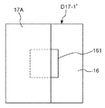
そして、デバイス搬送ヘッド17Aおよびデバイス搬送ヘッド17Bを開始位置Psに戻し(ステップS108)、ステップS102に戻り、撮像部である第1カメラ31は、第2位置情報(ステップS104において修正したエンコーダー値)に基づいて、検査部16(電子部品載置部)の第2像である1つの画像D17−2を撮像する(図25参照)。これにより、判断を行うのにより適した画像を得ることができる。
Then, the
そして、ステップS103で、画像D17−2において凹部161が映っていると判断した場合、ステップS105において、凹部161の中心が映っているか否かを判断する。なお、凹部161の中心とは、例えば、凹部161をZ方向からみたとき、各対角線が交わる部分であり、レーザー光L1が照射される部分である。
If it is determined in step S103 that the
ステップS105において、凹部161の中心が映っていない、すなわち、凹部161の一部がデバイス搬送ヘッド17Aまたはデバイス搬送ヘッド17Bに遮られていると判断した場合、デバイス搬送ヘッド17Bがどの位置であれば凹部161の中心が映るかを算出し(ステップS106)、画像D17−2を撮像した際に撮像指令信号を送信した時ときのエンコーダー値である第2位置情報を修正して、次の補正した位置情報である、第1位置情報および第2位置情報とは異なる第3位置情報を作成する(ステップS107)。すなわち、第1カメラ31(撮像部)に撮像された第2像である画像D17−1に基づいて、第3位置情報を作成する。このように、第3位置情報は、第2像である画像D17−2に含まれる少なくとも1つの把持部(デバイス搬送ヘッド17B)の像と、画像D17−2に含まれる凹部161(載置部)の像とに基づいて決められる。これにより、第3位置情報に基づいて撮像した場合、デバイス搬送ヘッド17Bが凹部161の全部を遮るのを防止または抑制することができる。その結果、判断を行うのにより適した画像を得ることができる。
If it is determined in step S105 that the center of the
そして、ステップS108において、デバイス搬送ヘッド17Aおよびデバイス搬送ヘッド17Bを開始位置Psに戻し、ステップS102において、第3位置情報に基づいて撮像を1回行い、第3像としての1つの画像D17−3を得る。
In step S108, the
そして、ステップS103において凹部161が映っていると判断し、ステップS105において、凹部161の中心が映っていると判断した場合、ステップS109において、実際の検査時に、撮像指令信号を送信する際のトリガーポイントとなるエンコーダー値として第3位置情報に決定する。
Then, when it is determined in step S103 that the
このように、電子部品搬送装置10では、制御部800は、少なくとも1つの把持部(本実施形態では、デバイス搬送ヘッド17B)の位置と、第1カメラ31(撮像部)が撮像した像における凹部161(載置部)の位置とに基づいて、第1カメラ31の撮像開始のタイミングを調整可能である。これにより、第1カメラ31が撮像した画像において、凹部161の中心が映るよう調整することができる。よって、撮像した画像に基づいて正確な判断を行うことができる。
As described above, in the electronic
また、検査部16(電子部品載置部)では、ICデバイス90(電子部品)の検査が行われるものであり、制御部800は、検査に先立って撮像指令信号を送信するタイミングを調整するため、検査中に撮像した画像において、凹部161の中心が映るよう調整することができる。よって、撮像した画像に基づいて正確な判断を行うことができる。
The inspection unit 16 (electronic component placement unit) inspects the IC device 90 (electronic component), and the
また、前記では、デバイス搬送ヘッド17Aおよびデバイス搬送ヘッド17Bが−Y側に移動しながらの撮像タイミングを調整する場合について説明したが、同様にして、デバイス搬送ヘッド17Aおよびデバイス搬送ヘッド17Bが+Y側に移動しながらの撮像タイミングを調整することもできる。さらに、Y方向に加え、Z方向に移動する場合についても、同様にして撮像タイミングを調整することができる。すなわち、デバイス搬送ヘッド17Aおよびデバイス搬送ヘッド17B(第1把持部および第2把持部)の移動方向に応じて、第1カメラ31(撮像部)の撮像開始のタイミングを調整可能である。これにより、デバイス搬送ヘッド17Aおよびデバイス搬送ヘッド17Bの移動方向によらず、撮像タイミングを調整することができる。
In the above description, the case where the imaging timing is adjusted while the
また、電子部品搬送装置10では、制御部800は、例えば、シャッター速度を調整することにより、第1カメラ31(撮像部)が撮像した画像の明るさに応じて、露光時間を調整可能である。これにより、より正確な判断を行うのに適した画像(例えば、第1判断を行うときには、レーザー光L1が鮮明に映っている画像)を得ることができる。
Moreover, in the electronic
なお、上記では、レーザー光源41および照明5の作動を停止した状態で撮像タイミングの調整を行った場合について説明したが、レーザー光源41および照明5を作動させた状態で撮像タイミングの調整を行ってもよい。これにより、撮像タイミングの調整や、露光時間の調整をさらに正確に行うことができる。
In the above description, the case where the imaging timing is adjusted while the operation of the
また、前記のような撮像タイミングの調整での条件(デバイス搬送ヘッド17Aおよびデバイス搬送ヘッド17Bの移動速度や、凹部161の配置形態等)をモニター300で設定することができる。図63は、モニター300の設定画面の一例を示す図である。
Further, the conditions for adjusting the imaging timing as described above (the moving speed of the
図63に示す構成では、デバイス搬送ヘッド17Aおよびデバイス搬送ヘッド17Bの移動速度を5段階で調整することができる。また、検査部16におけるY方向に並んだ凹部16の列の数も設定することができる。
In the configuration shown in FIG. 63, the moving speeds of the
なお、画像D17−3は、判断の際、凹部161の中心部のみをトリミングして用いられるのが好ましい。この場合、凹部161の中心と画像D17−3の中心が一致しているのが好ましい。これにより、トリミングした画像を可及的に小さくすることができる。その結果、制御部800とのデータのやり取りを迅速に行うことができる。
Note that it is preferable that the image D17-3 is used by trimming only the central portion of the
次に、図28に示すフローチャートに基づいて、検査中の制御部800の制御動作を説明する。以下の制御動作は、ICデバイス90を検査部16に搬送して検査を行い、検査部16からICデバイス90を除去した状態での制御動作である。
Next, based on the flowchart shown in FIG. 28, the control operation of the
まず、ステップS201において、レーザー光源41を作動させて、各凹部161にレーザー光L1を照射する(図5参照)。なお、このとき、本実施形態では、照明5は消灯させた状態としておく。これにより、次のステップS202で得られる画像D1または画像D2において、レーザー光L1のラインを際立たせることができる。
First, in step S201, the
次いで、ステップS202において、第1カメラ31を用いて検査部16を撮像する。これにより、図12または図13に示すような、画像D1(第1画像)または画像D2(第1画像)を得ることができる。なお、ステップS102における撮像は、図16および図17に示す撮像可能状態のときに行われる。なお、撮像が終わると、レーザー光L1の照射を停止する。
Next, in step S <b> 202, the
次いで、ステップS203において、残留状態か除去状態かを判断する。本実施形態では、予め、ずれ量ΔD2の画像D2を取得してメモリー802に記憶しておき、画像D2でのレーザー光L1のずれ量に基づいて、残留状態か除去状態かの判断が行われる。なお、ステップS203において、残留状態であると判断した場合には、後述するステップS205に移行する。
Next, in step S203, it is determined whether the remaining state or the removed state. In the present embodiment, an image D2 having a deviation amount ΔD2 is acquired in advance and stored in the
ステップS204において、除去状態であると判断した場合、デバイス搬送ヘッド17に把持異常が生じていないか否かを判断する。なお、把持異常とは、例えば、ICデバイス90をデバイス搬送ヘッド17が把持していない状態のことを言う。この把持異常は、例えば、デバイス搬送ヘッド17の吸引圧を検出することにより行われる。
If it is determined in step S204 that the device is in the removal state, it is determined whether or not a gripping abnormality has occurred in the
ステップS204において、把持異常が生じていると判断した場合、すなわち、電子部品載置部である検査部16にICデバイス90(電子部品)が配置されていると判断した場合、把持部であるデバイス搬送ヘッド17の作動を停止する。なお、ステップS205では、ICデバイス90を把持したまま、移動を停止する。これにより、残留状態で、搬送動作を継続するのを防止することができる。
If it is determined in step S204 that a gripping abnormality has occurred, that is, if it is determined that the IC device 90 (electronic component) is disposed in the
そして、ステップS206において、照明5を点灯して、検査部16全体に光L2を照射する。
In step S206, the
次いで、ステップS207において、第1カメラ31により検査部16を撮像する。これにより、図14または図15に示すような、画像D1’(第2画像)または画像D2’(第2画像)を得ることができる。なお、ステップS207における撮像は、図16および図17に示す撮像可能状態のときに行われる。
Next, in step S <b> 207, the
次いで、ステップS208において、残留状態か除去状態かを判断する。ステップS108では、前述したように、撮像した画像D1’および画像D2’に基づいて、ICデバイス90の色や、明るさを検出し、残留状態か除去状態かを判断する。本実施形態では、予め、除去状態の画像D2’を取得し、メモリー802に記憶しておき、得られた画像D1’または画像D2’と比較する。
Next, in step S208, it is determined whether the remaining state or the removed state. In step S108, as described above, based on the captured image D1 'and image D2', the color and brightness of the
ステップS208において残留状態であると判断した場合には、ステップS209において、残留状態であることを報知する。この報知は、報知部24を作動させることにより行われる。この報知により、オペレーターは、検査部16のICデバイス90を取り除き、残留状態を解消することができる。そして、オペレーターは、例えば、操作パネル700により、搬送再開のボタンを押すことができる。
If it is determined in step S208 that the state is the remaining state, in step S209, the remaining state is notified. This notification is performed by operating the
そして、ステップS210において、再開ボタンが押されたと判断した場合、ステップS211において、検査部16を再度撮像し、ステップS212において残留状態か除去状態かを判断する。なお、ステップS212では、第1判断を行ってもよく、第2判断を行ってもよく、第1判断および第2判断の双方を行ってもよい。また、ステップS212での判断に応じて、ステップS211で撮像する際にレーザー光源41を点灯させるか照明5を点灯させるか、または、双方を点灯させるかが決定される。また、ステップS211での撮像が完了したら、点灯させたレーザー光源41または照明5を消灯させる。
If it is determined in step S210 that the restart button has been pressed, in step S211, the
ステップS212において、除去状態であると判断した場合、ステップS213において、搬送を再開する。ステップS212において、残留状態であると判断した場合、ステップS209に戻り、残留状態であることを報知する。 If it is determined in step S212 that the state is the removal state, the conveyance is resumed in step S213. If it is determined in step S212 that the residual state is present, the process returns to step S209 to notify that the residual state is present.
このように本実施形態では、第1画像である画像D1または画像D2に基づいて判断(第1判断)を行った後に、第2画像である画像D1’または画像D2’に基づいて判断(第2判断)を行う。このように輝度が異なる光を照射して撮像した第1画像および第2画像を用いて2段階で残留状態か除去状態かを判断するため、その判断をより正確に行うことができる。 As described above, in the present embodiment, the determination (first determination) is performed based on the image D1 or the image D2 that is the first image, and then the determination (first determination) is performed based on the image D1 ′ or the image D2 ′ that is the second image. 2 judgment). As described above, since the first image and the second image captured by irradiating light with different luminances are used to determine whether the remaining state or the removed state is obtained in two stages, the determination can be performed more accurately.
また、電子部品搬送装置10では、上記判断は、デバイス搬送ヘッド13やデバイス搬送ヘッド20にも適用することができるが、検査領域A3のデバイス搬送ヘッド17に適用することにより、すなわち、電子部品載置部は、ICデバイス90の検査が行われる検査部16であるのが好ましい。これにより、検査部16において、残留状態か除去状態かを判断する構成とすることにより、ICデバイス90の検査を効率よく行うことができる。
In the electronic
以上説明したように、電子部品搬送装置10によれば、光照射部としてのレーザー光源41が第1輝度のレーザー光L1を出射した状態で検査部16(電子部品載置部)を撮像した第1画像である画像D1または画像D2と、レーザー光源41が第1輝度よりも小さい第2輝度の光L2を出射している状態で検査部16を撮像した第2画像である画像D1’または画像D2’とのうちの少なくとも一方の画像に基づいて、検査部16に電子部品であるICデバイス90が配置されているか否の判断を行う。
As described above, according to the electronic
これにより、電子部品載置部に対する電子部品の搬送動作を行った後に、電子部品が電子部品載置部に残留しているか否かを検出することができる。特に、輝度が異なる光を照射して撮像した2つの画像のうちの少なくとも一方の画像に基づいて、ICデバイス90が検査部16に残留しているか否かを判断するため、その判断をより正確に行うことができる。
Thus, it is possible to detect whether or not the electronic component remains on the electronic component placement unit after the electronic component carrying operation with respect to the electronic component placement unit is performed. In particular, since it is determined whether or not the
なお、第2輝度は、第1輝度よりも低ければよく、ゼロの状態、すなわち、照明5が光L2を照射していない状態も含む。
The second luminance only needs to be lower than the first luminance, and includes a zero state, that is, a state where the
<第2実施形態>
以下、図29〜図39を参照して本発明の電子部品搬送装置および電子部品検査装置の第2実施形態について説明するが、前述した実施形態との相違点を中心に説明し、同様の事項はその説明を省略する。
Second Embodiment
Hereinafter, the second embodiment of the electronic component transport device and the electronic component inspection device of the present invention will be described with reference to FIGS. 29 to 39, but the description will focus on the differences from the above-described embodiment, and the same matters will be described. Will not be described.
本実施形態は、制御部の制御動作が異なること以外は前記第1実施形態と略同様である。 This embodiment is substantially the same as the first embodiment except that the control operation of the control unit is different.
また、以下の制御動作は、ICデバイス90の検査を行うのに先立って行う、第1カメラ31(第2カメラ32についても同様)が撮像を行うタイミングの調整方法である。
The following control operation is a method for adjusting the timing at which the first camera 31 (the same applies to the second camera 32) performs imaging prior to the inspection of the
ステップS301において、まず、開始位置Psにデバイス搬送ヘッド17Aおよびデバイス搬送ヘッド17Bを配置する。開始位置Psは、例えば、図29に示すように、凹部161が見え始める位置である。
In step S301, first, the
次に、ステップS302において、デバイス搬送ヘッド17Aおよびデバイス搬送ヘッド17Bを−Y方向に向って終了位置Peまで、間欠的に移動させる。そして、デバイス搬送ヘッド17Aおよびデバイス搬送ヘッド17Bが停止しているときに、間隙Sを介して凹部161を複数回(本実施形態では、5回)撮像する(図29〜図38参照)。
Next, in step S302, the
なお、開始位置Psから終了位置Peまでの間に、どの位置で撮像を行うかは、デバイス搬送ヘッド17Aまたはデバイス搬送ヘッド17Bのエンコーダー値に基づいて、予めメモリー802に記憶されている。このエンコーダー値は、例えば、第1カメラ31の位置に応じて設定される。
本ステップでは、一例として、5枚の画像を撮像している。
Note that the position at which imaging is performed between the start position Ps and the end position Pe is stored in advance in the
In this step, five images are taken as an example.
図29および図30に示すように、開始位置Psにおいて撮像した画像DPsには、デバイス搬送ヘッド17Aが全面に写っており、凹部161は、写っていない。
As shown in FIGS. 29 and 30, in the image DPs picked up at the start position Ps, the
図31および図32に示すように、開始位置Psよりも−Y方向に移動した位置P17−1で撮像した画像D17−1’には、デバイス搬送ヘッド17Aの一部が映っており、凹部161の一部がデバイス搬送ヘッド17Aに遮られており、凹部161の残部が写っている。
As shown in FIGS. 31 and 32, an image D17-1 ′ picked up at a position P17-1 moved in the −Y direction from the start position Ps shows a part of the
図33および図34に示すように、位置P17−1よりも−Y方向に移動した位置P17−2で撮像した画像D17−2’には、デバイス搬送ヘッド17Aおよびデバイス搬送ヘッド17Bの一部が映っているものの、凹部161の中心が映っている。
As shown in FIGS. 33 and 34, in the image D17-2 ′ picked up at the position P17-2 moved in the −Y direction from the position P17-1, a part of the
図35および図36に示すように、位置P17−2よりも−Y方向に移動した位置P17−3で撮像した画像D17−3’には、デバイス搬送ヘッド17Bの一部が映っており、凹部161の一部がデバイス搬送ヘッド17Bに遮られており、凹部161の残部が写っている。
As shown in FIGS. 35 and 36, a part of the
図37および図38に示すように、終了位置Peにおいて撮像した画像DPeには、デバイス搬送ヘッド17Bが全面に写っており、凹部161は、写っていない。
As shown in FIGS. 37 and 38, in the image DPe picked up at the end position Pe, the
このように、ステップS302では、停止している状態で、複数枚(本実施形態では、5枚)の画像を撮像する。 As described above, in step S302, a plurality of images (in this embodiment, five images) are captured in a stopped state.
次に、ステップS303において、画像DPs、画像D17−1’、画像D17−2’、画像D17−3’および画像DPeから判断に適した画像、すなわち、凹部161の中心が写っている画像(画像D17−2’)を選択する。
Next, in step S303, an image suitable for determination from the image DPs, the image D17-1 ′, the image D17-2 ′, the image D17-3 ′, and the image DPe, that is, an image in which the center of the
次に、ステップS304において、選択した画像D17−2’を撮像したとき、すなわち、位置P17−2におけるエンコーダー値を記憶する。 Next, in step S304, when the selected image D17-2 'is captured, that is, the encoder value at the position P17-2 is stored.
次に、ステップS305において、デバイス搬送ヘッド17Aおよびデバイス搬送ヘッド17Bを開始位置Psに戻す。
Next, in step S305, the
そして、ステップS306において、デバイス搬送ヘッド17Aおよびデバイス搬送ヘッド17Bを開始位置Psから終了位置Peに向って移動させつつ、エンコーダー値に基づいて、位置P17−2のときに撮像を行う。本ステップでは、デバイス搬送ヘッド17Aおよびデバイス搬送ヘッド17Bを連続的に移動させつつ、動いている状態で、位置P17−2において撮像を行う。
In step S306, the
次いで、ステップS307において、ステップS306で撮像した画像と、ステップS303で選択した画像とを比較する。以下、一例として、ステップS306で撮像した画像が、図36に示す画像D17−3’であった場合について説明する。 In step S307, the image captured in step S306 is compared with the image selected in step S303. Hereinafter, as an example, a case will be described in which the image captured in step S306 is an image D17-3 'illustrated in FIG.
位置P17−2のときに撮像を行っても、得られた画像が、画像D17−2’ではなく、画像D17−3’である場合、画像D17−2’におけるデバイス搬送ヘッド17Bの位置と、画像D17−3におけるデバイス搬送ヘッド17Bの位置とに基づいて、制御部800が撮像指令信号を送信してから、実際に第1カメラ31が撮像を行うまでの間に、デバイス搬送ヘッド17Bがどれだけ移動したかを算出する。
Even if imaging is performed at the position P17-2, if the obtained image is not the image D17-2 ′ but the image D17-3 ′, the position of the
この算出は、デバイス搬送ヘッド17Bのうち、画像D17−2および画像D17−3の双方に写っている部分のうち、任意の部分(例えば、端部)同士を比較し、移動量を算出する。
This calculation calculates an amount of movement by comparing arbitrary portions (for example, end portions) among the portions of the
そして、ステップS308において、位置P17−2でのデバイス搬送ヘッド17Aおよびデバイス搬送ヘッド17Bのエンコーダー値に、前記移動量を考慮して、撮像指令信号を送信するエンコーダー値を算出する。すなわち、デバイス搬送ヘッド17Aおよびデバイス搬送ヘッド17Bが、位置P17−2よりも、移動量分、+Y側に位置しているときのエンコーダー値(補正後エンコーダー値)を算出する。この補正後エンコーダー値のときに、撮像指令信号を第1カメラ31に送信すれば、画像D17−2を得ることができる。
In step S308, an encoder value for transmitting an imaging command signal is calculated in consideration of the amount of movement in the encoder values of the
このように、制御部800は、撮像部である第1カメラ31に対して撮像指令信号を送信するタイミングを調整可能である。具体的には、撮像部である第1カメラ31が撮像を開始するタイミングを調整可能である。これにより、撮像指令信号を送信してから、実際に第1カメラ31が撮像を開始するまでのタイムラグを考慮して、第1カメラ31に撮像指令信号を送信することができる。よって、タイムラグがあるにも関わらず、所望の画像、すなわち、判断に適した画像(画像D17−3)を得ることができる。
As described above, the
以上説明したように、本実施形態では、制御部800は、第1カメラ31(撮像部)の撮像結果(画像D17−2’)と第1位置情報(画像D17−2’を撮像したときのエンコーダー値)に基づいて、第1カメラ31に対して撮像指令信号を送信するタイミングを決定(調整)する第1調整(ステップS304)を行う。そして、制御部800は、第1調整後に、撮像指令信号を送信してから第1カメラ31が撮像を開始するまでの少なくとも1つの把持部(デバイス搬送ヘッド17B)の移動量に基づいて、第1カメラ31に対して撮像指令信号を送信するタイミングを調整する第2調整を行う。これにより、第1カメラ31の個体差に関わらず、撮像指令信号を送信してから、実際に第1カメラ31が撮像を開始するまでのタイムラグを考慮して、撮像指令信号を最適なタイミングで送信することができる。その結果、第1カメラ31の個体差に関わらず、判断に適した画像(画像D17−3’)を得ることができる。
As described above, in the present embodiment, the
なお、画像D17−3’は、判断の際、凹部161の中心部のみをトリミングして用いられるのが好ましい。この場合、凹部161の中心と画像D17−3’の中心が一致しているのが好ましい。これにより、トリミングした画像を可及的に小さくすることができる。その結果、制御部800とのデータのやり取りを迅速に行うことができる。
Note that it is preferable that the image D17-3 'is used by trimming only the central portion of the
<第3実施形態>
以下、図40を参照して本発明の電子部品搬送装置および電子部品検査装置の第3実施形態について説明するが、前述した実施形態との相違点を中心に説明し、同様の事項はその説明を省略する。
<Third Embodiment>
Hereinafter, the third embodiment of the electronic component transport apparatus and the electronic component inspection apparatus according to the present invention will be described with reference to FIG. 40. The description will focus on the differences from the above-described embodiment, and the same matters will be described. Is omitted.
本実施形態は、制御部の制御動作が異なること以外は前記第1実施形態と略同様である。 This embodiment is substantially the same as the first embodiment except that the control operation of the control unit is different.
なお、以下の制御動作は、ICデバイス90を検査部16に搬送して検査を行い、検査部16からICデバイス90を除去した状態での制御動作である。
The following control operation is a control operation in a state where the
まず、ステップS401において、第1判断を行うか第2判断を行うかを選択する。ステップS401では、光照射部であるレーザー光源41や照明5の照射条件、検査部16(電子部品載置部)の色、ICデバイス90(電子部品)の色、第1カメラ31の分解能のうちの少なくとも1つの条件に基づいて、第1画像(画像D1、D2)および第2画像(画像D1’、画像D2’)から、残留状態か除去状態かの判断の際に用いる画像を選択する。これにより、残留状態か除去状態かの判断を行うのに際し、より良い条件の画像を用いることができる。よって、ICデバイス90が検査部16に残留しているか否かをより正確に判断することができる。
First, in step S401, it is selected whether to perform the first determination or the second determination. In step S <b> 401, among the irradiation conditions of the
なお、照射条件とは、例えば、レーザー光L1の出射角度や、レーザー光L1の輝度や、光L2の輝度等が挙げられる。これらの条件と、例えば、検査領域A3内の明るさとの検量線を予めメモリー802に記憶しておき、検量線に基づいて、ステップS401の判断を行うことができる。
The irradiation conditions include, for example, the emission angle of the laser light L1, the brightness of the laser light L1, the brightness of the light L2, and the like. A calibration curve between these conditions and, for example, the brightness in the inspection area A3 can be stored in the
ステップS401において第1画像を用いると判断した場合、ステップS402において、レーザー光源41を作動させて、各凹部161にレーザー光L1を照射する(図5参照)。
When it is determined in step S401 that the first image is used, in step S402, the
そして、ステップS403において、第1カメラ31を用いて検査部16を撮像する。これにより、図12または図13に示すような、画像D1(第1画像)または画像D2(第1画像)を得ることができる。
In step S <b> 403, the
次いで、ステップS404において、第1実施形態のステップS203と同様に、残留状態か除去状態かを判断する。ステップS404において、残留状態であると判断した場合、ステップS405において、デバイス搬送ヘッド17の作動を停止し、ステップS406において、報知部24により、残留状態であることを報知する。
Next, in step S404, as in step S203 of the first embodiment, it is determined whether the state is a residual state or a removed state. If it is determined in step S404 that the device is in the remaining state, the operation of the
そして、ステップS407において、再開ボタンが押されたと判断した場合、ステップS408において、検査部16を再度撮像し、ステップS409において残留状態か除去状態かを判断する。なお、ステップS409では、第1判断を行ってもよく、第2判断を行ってもよく、第1判断および第2判断の双方を行ってもよい。また、ステップS409での判断に応じて、ステップS408で撮像する際にレーザー光源41を点灯させるか照明5を点灯させるか、または、双方を点灯させるかが決定される。また、ステップS408での撮像が完了したら、点灯させたレーザー光源41または照明5を消灯させる。
If it is determined in step S407 that the resume button has been pressed, the
ステップS409において、除去状態であると判断した場合、ステップS410において、搬送を再開する。ステップS409において、残留状態であると判断した場合、ステップS206に戻り、残留状態であることを報知する。 If it is determined in step S409 that the state is the removal state, the conveyance is resumed in step S410. If it is determined in step S409 that the state is the remaining state, the process returns to step S206 to notify the remaining state.
なお、ステップS401において、第2画像を用いる、すなわち、第2判断を行うと判断した場合、ステップS411において、照明5を点灯させ、ステップS412において、第1カメラ31により検査部16を撮像し、第2画像を得る。そして、ステップS413において、第1実施形態でのステップS208と同様にして、残留状態か除去状態かを判断する。ステップS413において、残留状態であると判断した場合、ステップS405に移行し、以下のステップを行う。
In step S401, when it is determined that the second image is used, that is, the second determination is performed, the
<第4実施形態>
以下、図41〜図43を参照して本発明の電子部品搬送装置および電子部品検査装置の第3実施形態について説明するが、前述した実施形態との相違点を中心に説明し、同様の事項はその説明を省略する。
<Fourth embodiment>
Hereinafter, a third embodiment of the electronic component transport device and the electronic component inspection device of the present invention will be described with reference to FIGS. 41 to 43. The difference between the third embodiment and the above-described embodiment will be mainly described, and similar matters will be described. Will not be described.
本実施形態は、制御部の制御動作が異なること以外は前記第1実施形態と略同様である。 This embodiment is substantially the same as the first embodiment except that the control operation of the control unit is different.
図41に示すように、本実施形態では、検査部16の+X側には、照度を検出する照度センサー25が設けられている。この照度センサー25は、図示はしないが、制御部800と電気的に接続されており、照度センサー25が検出した照度の情報は、制御部800に送信される。
As shown in FIG. 41, in this embodiment, an
また、検査部16の上面のうち、−X軸側の端部近傍には、マーカー26が設けられている。マーカー26は、互いに色が異なる領域を有する着色部等により構成されている。
Further, a
次に、図43に示すフローチャートを用いて、本実施形態での制御部800の制御動作について説明するが、以下の制御動作は、ICデバイス90を検査部16に搬送して検査を行い、検査部16からICデバイス90を除去した状態での制御動作である。
Next, the control operation of the
まず、ステップS501において、レーザー光源41および照明5を点灯させる。このとき、レーザー光L1を際立たせるためには、光L2の輝度を小さくするのが好ましいが、光L2の輝度が小さすぎると、第2判断を正確に行うのが困難になる可能性が有る。
First, in step S501, the
そこで、ステップS502において、レーザー光L1および光L2のうちの少なくとも一方の輝度の調整を行う。なお、この調整は、照度センサー25が検出した照度の情報(検査領域A3内の明るさ)または画像の輝度分布から得られる情報等に応じて、レーザー光源41および照明5のうちの少なくとも一方の出力を調整することにより行われる。
Therefore, in step S502, the brightness of at least one of the laser light L1 and the light L2 is adjusted. This adjustment is performed at least one of the
そして、この調整状態で、ステップS503において、第1カメラ31を用い、図42に示す画像D3を撮像する。この画像D3は、図12および図13に示す画像D1、D2よりも大きく、凹部161の周辺部も撮像されているものである。
In this adjusted state, in step S503, the
そして、ステップS504において、残留状態か除去状態かの判断を行う。ステップS504の判断は、第1実施形態でのステップS208と同様にして行われる。なお、ステップS504では、例えば、図42に示すように、検査部16の上面にICデバイス90が不本意に配置されてしまった場合であっても、そのことを検出することができる。なお、本実施形態では、この場合も残留状態に含む。特に、検査部16の上面にICデバイス90が不本意に配置されてしまった場合、本実施形態では、レーザー光L1のラインがICデバイス90の上面にてX方向の位置がずれる。このため、検査部16の上面にICデバイス90が不本意に配置されてしまったことを正確に検出することができる。
In step S504, it is determined whether the remaining state or the removed state. The determination in step S504 is performed in the same manner as in step S208 in the first embodiment. In step S504, for example, as shown in FIG. 42, even if the
ステップS504において、残留状態であると判断した場合には、ステップS505において、デバイス搬送ヘッド17の作動を停止させ、ステップS506において、報知部24により、残留状態であることを報知する。
If it is determined in step S504 that the device is in the remaining state, the operation of the
そして、ステップS507において、再開ボタンが押されたと判断した場合、ステップS508において、検査部16を再度撮像し、ステップS509において残留状態か除去状態かを判断する。なお、ステップS509では、第1判断を行ってもよく、第2判断を行ってもよく、第1判断および第2判断の双方を行ってもよい。また、ステップS509での判断に応じて、ステップS508で撮像する際にレーザー光源41を点灯させるか照明5を点灯させるか、または、双方を点灯させるかが決定される。また、ステップS508での撮像が完了したら、点灯させたレーザー光源41または照明5を消灯させる。
If it is determined in step S507 that the restart button has been pressed, the
ステップS509において、除去状態であると判断した場合、ステップS510において、搬送を再開する。ステップS509において、残留状態であると判断した場合、ステップS506に戻り、残留状態であることを報知する。 If it is determined in step S509 that the state is the removal state, the conveyance is resumed in step S510. If it is determined in step S509 that the state is the remaining state, the process returns to step S506 to notify the remaining state.
<第5実施形態>
以下、図44を参照して本発明の電子部品搬送装置および電子部品検査装置の第5実施形態について説明するが、前述した実施形態との相違点を中心に説明し、同様の事項はその説明を省略する。
<Fifth Embodiment>
Hereinafter, the fifth embodiment of the electronic component transport device and the electronic component inspection device of the present invention will be described with reference to FIG. 44. The difference from the above-described embodiment will be mainly described, and the same matters will be described. Is omitted.
本実施形態は、カメラが3つ設けられていること以外は前記第1実施形態と同様である。 This embodiment is the same as the first embodiment except that three cameras are provided.
図44に示すように、本実施形態では、撮像部は、第1画像である画像D1、D2を撮像する第1撮像部である第1カメラ31と、第2撮像部である第2カメラ32とに加え、第2画像である画像D1’、D2’を撮像する第3撮像部であるカメラ34とを有する。すなわち、本実施形態では、画像D1、D2を撮像する専用の第1カメラ31および第2カメラ32と、画像D1’、D2’を撮像する専用のカメラ34とを有する構成となっている。このため、第1カメラ31および第2カメラ32を比較的高い分解能を有するものとし、カメラ34を、第1カメラ31および第2カメラ32よりも低い分解能を有するものとすることができる。その結果、第2判断において、制御部800とカメラ34との間でのデータのやり取りにかかる時間を短縮することができる。
As shown in FIG. 44, in this embodiment, the imaging unit includes a
<第6実施形態>
以下、図45〜図47を参照して本発明の電子部品搬送装置および電子部品検査装置の第6実施形態について説明するが、前述した実施形態との相違点を中心に説明し、同様の事項はその説明を省略する。
<Sixth Embodiment>
Hereinafter, the sixth embodiment of the electronic component transport device and the electronic component inspection device of the present invention will be described with reference to FIGS. 45 to 47. However, the difference from the above-described embodiment will be mainly described, and similar matters will be described. Will not be described.
本実施形態は、制御部800の制御動作が異なること以外は前記第1実施形態と同様である。
This embodiment is the same as the first embodiment except that the control operation of the
以下、図45に示すフローチャートを用いて本実施形態での制御部800の制御動作について説明するが、以下の制御動作は、ICデバイス90を検査部16に搬送して検査を行うのに先立って行われる制御動作である。
Hereinafter, the control operation of the
まず、ステップS601に示すように、照明5を作動させて、光L2を出射する。そして、第1カメラ31により、検査部16を撮像する(ステップS602)。次いで、ステップS603において、照明5を消灯させる。
First, as shown in step S601, the
次いで、ステップS604において、レーザー光源41を作動させて、レーザー光L1を検査部16に照射し、その状態で第1カメラ31により、検査部16を撮像する(ステップS405)。
Next, in step S604, the
そして、ステップS606において、ミラー42のモーター43を回動させて、レーザー光L1の照射位置を調整する。この調整は、ステップS602で撮像された画像において、中心位置Pcを割り出し(図46参照)、この中心位置Pcの座標を記憶し、ステップS405で撮像された画像において、レーザー光L1が、中心位置Pcに位置するまで調整する(図47参照)。これにより、レーザー光L1をより確実に凹部161に照射することができる。特に、検査部16の凹部161の数や配置形態は、テスト毎に異なる場合があり、この場合、検査部16の凹部161の位置に合わせて、画像を取得することができる。
In step S606, the
なお、本実施形態では、レーザー光L1の調整は、光反射部33の回動角度と、レーザー光L1の照射位置との検量線に基づいて行われる。
In the present embodiment, the adjustment of the laser beam L1 is performed based on a calibration curve between the rotation angle of the
<第7実施形態>
以下、図48を参照して本発明の電子部品搬送装置および電子部品検査装置の第7実施形態について説明するが、前述した実施形態との相違点を中心に説明し、同様の事項はその説明を省略する。
<Seventh embodiment>
Hereinafter, the seventh embodiment of the electronic component transport device and the electronic component inspection device of the present invention will be described with reference to FIG. 48, but the description will focus on the differences from the above-described embodiment, and the same matters will be described. Is omitted.
本実施形態は、検査部にマーカーおよび表示部が設けられていること以外は、前記第6実施形態と同様である。 This embodiment is the same as the sixth embodiment except that the inspection unit is provided with a marker and a display unit.
図48に示すように、本実施形態では、検査部16の上面に、マーカー27と、表示部28とが設けられている。
As shown in FIG. 48, in this embodiment, a
マーカー27は、各凹部161の縁部に設けられており、凹部161におけるX方向の中心位置Pcを示すものである。このマーカー27に合わせて、レーザー光L1の照射位置を合わせることにより、ステップS402における撮像を省略することができる。よって、レーザー光L1の照射位置の調整工程の簡素化を図ることができる。
The
また、表示部28は、例えば、二次元バーコードで構成されている。レーザー光L1の照射位置の調整工程終了後に、表示部28を読み取り、レーザー光L1の照射位置と表示部28の情報とを紐づけてメモリー802に記憶しておくことができる。これにより、例えば、検査毎に凹部161の配置形態が異なる検査部16を使用したとしても、表示部28を読み取ることにより、レーザー光L1の照射位置が分かる。すなわち、レーザー光L1の照射位置の再現性を高めることができる。よって、レーザー光L1の照射位置の調整を簡単に行うことができる。
Moreover, the
<第8実施形態>
以下、図49を参照して本発明の電子部品搬送装置および電子部品検査装置の第8実施形態について説明するが、前述した実施形態との相違点を中心に説明し、同様の事項はその説明を省略する。
<Eighth Embodiment>
The eighth embodiment of the electronic component transport apparatus and the electronic component inspection apparatus of the present invention will be described below with reference to FIG. 49. The description will focus on the differences from the above-described embodiment, and the same matters will be described. Is omitted.
本実施形態は、光の出射タイミングが異なること以外は前記第1実施形態と同様である。 This embodiment is the same as the first embodiment except that the light emission timing is different.
本実施形態では、レーザー光源41は、間欠的にレーザー光L1を照射する。すなわち、レーザー光源41は、レーザー光L1の照射と停止とを交互に繰り返す構成となっている。また、本実施形態でのレーザーパワーは、IEC 60825−1:2014や、JISはC 6802:2014に準じて設定される。これにより、オペレーターの安全性が確保される。
In the present embodiment, the
図49に示すタイミングチャートでは、図中上側のチャートが、第1カメラ31を示し、図中下側のチャートが、レーザー光源41を示している。図49に示すように、本実施形態では、光照射部であるレーザー光源41は、撮像開始時刻t1よりも先にレーザー光L1を照射し、撮像終了時刻t2よりも後にレーザー光L1の照射を停止する。これにより、第1カメラ31が撮像している間は、レーザー光L1を検査部16に照射している状態とすることができる。
In the timing chart shown in FIG. 49, the upper chart in the drawing shows the
さらに、光照射部であるレーザー光源41が、撮像可能なときにレーザー光L1を照射する構成とすることにより、検査部が、デバイス搬送ヘッド17に遮られるときに撮像するのを防止することができる。よって、無駄なく撮像を行うことができる。
Further, by adopting a configuration in which the
<第9実施形態>
以下、図50および図51を参照して本発明の電子部品搬送装置および電子部品検査装置の第9実施形態について説明するが、前述した実施形態との相違点を中心に説明し、同様の事項はその説明を省略する。
<Ninth Embodiment>
Hereinafter, the ninth embodiment of the electronic component transport apparatus and the electronic component inspection apparatus of the present invention will be described with reference to FIGS. 50 and 51. However, the differences from the above-described embodiment will be mainly described, and similar matters will be described. Will not be described.
本実施形態は、制御部の制御動作および検査部の凹部の配置形態が異なること以外は前記第1実施形態と同様である。 This embodiment is the same as the first embodiment except that the control operation of the control unit and the arrangement of the recesses of the inspection unit are different.
図50に示すように、本実施形態では、検査部16には、8つの凹部161が設けられている。検査部16では、4つの凹部161がX方向に一列に並んで配置され、その列の+Y側にさらに4つの凹部161が一列に並んで配置されている。
As shown in FIG. 50, in the present embodiment, the
このような検査部16では、検査部16のX方向の中心よりも+X側の4つの凹部161におけるレーザー光L1の照射および撮像を検出ユニット2Aが担い、検査部16のX方向の中心よりも−X側の4つの凹部161におけるレーザー光L1の照射および撮像を検出ユニット2Bが担う。以下、検出ユニット2Aと、検査部16のX方向の中心よりも+X側の4つの凹部161とを代表的に説明する。
In such an
第1実施形態で述べたように、検出ユニット2Aでは、4つのレーザー光源41が設けられており、1つのレーザー光源41でY方向に並ぶ2つの凹部161にレーザー光L1を照射する。このため、図50に示すような凹部161の配置形態であると、2つのレーザー光源41を作動させればよいため、検出ユニット2Aにおいて、4つのレーザー光源41のうち、2つのレーザー光源41を選択して作動させる。なお、4つのレーザー光源41を、+X側から順にレーザー光源41A、レーザー光源41B、レーザー光源41Cおよびレーザー光源41Dとする。
As described in the first embodiment, in the
この選択の際、前述したように、レーザー光L1の入射角θ1を大きくすれば大きくするほど、第1判断を正確に行うことができる。よって、検出ユニット2Aのうち、+X側のレーザー光源41Aおよびレーザー光源41Bが選択される(図51参照)。
In this selection, as described above, the first determination can be performed more accurately as the incident angle θ1 of the laser beam L1 is increased. Therefore, the
なお、例えば、レーザー光源41Aのレーザー光L1の入射角θ1が、凹部161の内周面162とZ方向とのなす角度θ2よりも大きかった場合には、レーザー光源41Aを選択するのを省略し、レーザー光源41Bおよびレーザー光源41Cを選択する(図示せず)。
For example, when the incident angle θ1 of the laser light L1 of the
このように、本実施形態では、入射角θ1<角度θ2を満足しつつ、入射角θ1が可及的に大きくなるようレーザー光源41の選択を行う。これにより、検査部16における凹部161の配置形態を問わず、第1判断を正確に行うことができる。
Thus, in this embodiment, the
<第10実施形態>
以下、図52を参照して本発明の電子部品搬送装置および電子部品検査装置の第10実施形態について説明するが、前述した実施形態との相違点を中心に説明し、同様の事項はその説明を省略する。
<Tenth Embodiment>
Hereinafter, a tenth embodiment of the electronic component transport apparatus and the electronic component inspection apparatus of the present invention will be described with reference to FIG. 52. The difference from the above-described embodiment will be mainly described, and the same matters will be described. Is omitted.
本実施形態は、検査部における凹部の配置形態と、第1撮像部および第2撮像部の撮像範囲とが異なること以外は前記第1実施形態と同様である。 The present embodiment is the same as the first embodiment except that the arrangement form of the recesses in the inspection unit and the imaging ranges of the first imaging unit and the second imaging unit are different.
図52に示すように、本実施形態では、検査部16には、14個の凹部161が設けられている。検査部16では、7つの凹部161がX方向に一列に並んで配置され、その列の+Y側にさらに7つの凹部161が一列に並んで配置されている。また、凹部161は、X方向に沿った1つの列において、奇数個の凹部161が設けられているため、検査部16のX方向の中心部に凹部161が配置されている。
As shown in FIG. 52, in the present embodiment, the
また、本実施形態では、検出ユニット2Aの第1カメラ31と、検出ユニット2Bの第1カメラ31との撮像範囲が互いに重なり合った重なり部を有している。具体的には、検出ユニット2Aの第1カメラ31は、+X側から4つの凹部161を撮像し、検出ユニット2Bの第1カメラ31は、−X側から4つの凹部161を撮像する。このため、真ん中の凹部161(凹部161D)は、検出ユニット2Aの第1カメラ31と、検出ユニット2Bの第1カメラ31との双方に撮像されている。すなわち、検出ユニット2Aの第1カメラ31が撮像する画像D31Aにも映っており、検出ユニット2Bの第1カメラ31が撮像する画像D31Bにも映っている。なお、このことは、検出ユニット2Aの第2カメラ32が撮像する画像D32Aと、検出ユニット2Bの第2カメラ32が撮像する画像D32Bにおいても同様である。
In the present embodiment, the imaging ranges of the
このような構成によれば、X方向の中心部に凹部161が位置している検査部16であっても、中心部に位置している凹部161Dを確実に撮像することができる。すなわち、凹部161Dが、画像D31Aおよび画像D31Bの境界部に位置するのを防止することができる(画像D32Aおよび画像D32Bについても同様)。よって、凹部161におけるICデバイス90の有無の判断を正確に行うことができる。
According to such a structure, even if it is the test |
なお、凹部161Dにおける判断は、画像D31Aおよび画像D31Bのうちの少なくとも一方に基づいて行うことができる(画像D32Aおよび画像D32Bについても同様)。 Note that the determination in the recess 161D can be made based on at least one of the image D31A and the image D31B (the same applies to the image D32A and the image D32B).
また、第1カメラ31および第2カメラ32として、CCDカメラを採用した場合、図36中左右方向に順次露光を行い、図36中上下方向に順次読み出しを行う。本実施形態では、第1カメラ31および第2カメラ32が撮像する画像が図中左右方向を長手方向とする形状をなしているため、図中上下方向の読み出し回数が増大するのを抑制することができる。その結果、撮像した画像の読み出しに係る時間を短縮することができ、画像に基づいた判断を円滑に行うことができる。
When CCD cameras are employed as the
<第11実施形態>
以下、図53を参照して本発明の電子部品搬送装置および電子部品検査装置の第11実施形態について説明するが、前述した実施形態との相違点を中心に説明し、同様の事項はその説明を省略する。
本実施形態は、制御部の制御動作が異なること以外は前記第1実施形態と同様である。
<Eleventh embodiment>
Hereinafter, the eleventh embodiment of the electronic component transport apparatus and the electronic component inspection apparatus of the present invention will be described with reference to FIG. 53, but the difference from the above-described embodiment will be mainly described, and the same matters will be described. Is omitted.
This embodiment is the same as the first embodiment except that the control operation of the control unit is different.
本実施形態では、第1実施形態でのステップS205において、搬送を停止した際、図53に示すように、デバイス搬送ヘッド17Aおよびデバイス搬送ヘッド17Bは、互いに反対方向に移動する。これにより、デバイス搬送ヘッド17Aおよびデバイス搬送ヘッド17Bの間隙Sが広がる。
In the present embodiment, when transport is stopped in step S205 in the first embodiment, as shown in FIG. 53, the
そして、この間隙Sが広がった状態で、ステップS206およびステップS207を経て、第2画像を撮像する。これにより、間隙Sが広がった分、一度の撮像において、検査部16のより多くの領域が撮像された第2画像を得ることができる。その結果、ステップS207での撮像の簡略化を図ることができる。
Then, in a state where the gap S is widened, the second image is captured through steps S206 and S207. Thereby, since the gap S is widened, it is possible to obtain a second image in which more areas of the
<第12実施形態>
以下、図54および図55を参照して本発明の電子部品搬送装置および電子部品検査装置の第12実施形態について説明するが、前述した実施形態との相違点を中心に説明し、同様の事項はその説明を省略する。
<Twelfth embodiment>
The twelfth embodiment of the electronic component transport apparatus and the electronic component inspection apparatus according to the present invention will be described below with reference to FIGS. 54 and 55. The difference from the above-described embodiment will be mainly described, and the same matters will be described. Will not be described.
本実施形態は、デバイス搬送ヘッドの動作が異なること以外は前記第1実施形態と同様である。 The present embodiment is the same as the first embodiment except that the operation of the device transport head is different.
図54および図55に示すように、本実施形態では、デバイス搬送ヘッド17Aおよびデバイス搬送ヘッド17Bは、それぞれ、検査部16の凹部161に対応する吸着部(図示せず)を有しており、交互に検査部16へのICデバイス90(図示せず)の搬送を行う。
As shown in FIGS. 54 and 55, in the present embodiment, the
すなわち、図54に示すように、デバイス搬送ヘッド17Bが検査部16に対してICデバイス90を搬送しているときには、デバイス搬送ヘッド17Aは、検査部16の−Y側に外れた位置に位置している。一方、図55に示すように、デバイス搬送ヘッド17Aが検査部16に対してICデバイス90を搬送しているときには、デバイス搬送ヘッド17Bは、検査部16の+Y側に外れた位置に位置している。
That is, as shown in FIG. 54, when the
このように、本実施形態では、検査部16に対して、一方のデバイス搬送ヘッド17がICデバイス90の搬送を行い、これを交互に繰り返す構成となっている。
このような第12実施形態によっても前記第1実施形態と同様の効果を奏する。
Thus, in the present embodiment, one
The twelfth embodiment has the same effect as the first embodiment.
<第13実施形態>
以下、図56〜図58を参照して本発明の電子部品搬送装置および電子部品検査装置の第13実施形態について説明するが、前述した実施形態との相違点を中心に説明し、同様の事項はその説明を省略する。
<13th Embodiment>
Hereinafter, a thirteenth embodiment of the electronic component transport apparatus and the electronic component inspection apparatus of the present invention will be described with reference to FIGS. 56 to 58. The difference from the above-described embodiment will be mainly described, and similar matters will be described. Will not be described.
本実施形態は、デバイス搬送ヘッドの動作が異なること以外は前記第1実施形態と同様である。 The present embodiment is the same as the first embodiment except that the operation of the device transport head is different.
本実施形態の検査部16は、X方向に凹部161が並んだ列が、Y方向に4列設けられている。
In the
デバイス搬送ヘッド17Aおよびデバイス搬送ヘッド17Bは、上記4列の凹部161のうち、2列ずつを担当する。
The
具体的には、図56に示すように、+Y側の2列の凹部161へのICデバイス90(図示せず)の搬送を、デバイス搬送ヘッド17Bが担い、−Y側の2列の凹部161へのICデバイス90(図示せず)の搬送を、デバイス搬送ヘッド17Aが担っている。
Specifically, as shown in FIG. 56, the
また、図57に示すように、検査部16からICデバイス90を搬出するとき等には、デバイス搬送ヘッド17Bは、+Y側に移動し、デバイス搬送ヘッド17Aは、−Y側に移動する(図57中矢印α17Aおよび矢印α17B参照)。すなわち、デバイス搬送ヘッド17Aおよびデバイス搬送ヘッド17Bは、Z方向から見た際、互いに接近離間を繰り返すように移動する。
As shown in FIG. 57, when the
なお、図58に示すように、デバイス搬送ヘッド17Aおよびデバイス搬送ヘッド17Bは、互いに離間する際、Y方向およびZ方向に移動することができるため、円弧を描くように移動することができる(図58中矢印α17Aおよび矢印α17B参照)。
このような第13実施形態によっても前記第1実施形態と同様の効果を奏する。
As shown in FIG. 58, since the
The thirteenth embodiment also has the same effects as the first embodiment.
<第14実施形態>
以下、図59を参照して本発明の電子部品搬送装置および電子部品検査装置の第14実施形態について説明するが、前述した実施形態との相違点を中心に説明し、同様の事項はその説明を省略する。
<Fourteenth embodiment>
Hereinafter, the fourteenth embodiment of the electronic component transport apparatus and the electronic component inspection apparatus according to the present invention will be described with reference to FIG. 59. The difference from the above-described embodiment will be mainly described, and the same matters will be described. Is omitted.
本実施形態は、撮像部に制御部が設けられていること以外は前記第1実施形態と同様である。 This embodiment is the same as the first embodiment except that the imaging unit is provided with a control unit.
図59に示すように、本実施形態では、制御部800とは、別途に、第1カメラ31および第2カメラ32には、それぞれ、制御部803が内蔵されている。すなわち、電子部品搬送装置10は、制御部800(第1制御部)と、制御部803(第2制御部)とを有している。以下、第1カメラ31の制御部803を代表的に説明する。
As shown in FIG. 59, in the present embodiment, the
制御部803は、第1カメラ31の撮像素子への露光を複数回(例えば、2回)行い、その画像に基づいて、第1判断および第2判断のうちの少なくとも一方の判断を行う。そして、制御部803は、その判断結果を、制御部800に送信する。
The
制御部800は、送信された判断結果に基づいて、デバイス搬送ヘッド17Aおよびデバイス搬送ヘッド17Bの作動を停止させたり、モニター300およびスピーカー500により、判断結果の報知を行ったりする。
Based on the transmitted determination result, the
このような本実施形態によれば、制御部800と第1カメラ31(第2カメラ32についても同様)との間での画像データの通信を省略し、判断結果のみを電気信号で送信するため、第1判断および第2判断の高速化を図ることができる。さらに、判断後の動作を迅速に行うことができ、電子部品搬送装置10のスループットの低下を効果的に抑制することができる。
According to this embodiment, communication of image data between the
以上、本発明の電子部品搬送装置および電子部品検査装置を図示の実施形態について説明したが、本発明は、これに限定されるものではなく、電子部品搬送装置および電子部品検査装置を構成する各部は、同様の機能を発揮し得る任意の構成のものと置換することができる。また、任意の構成物が付加されていてもよい。 As mentioned above, although the electronic component conveyance apparatus and electronic component inspection apparatus of this invention were demonstrated about embodiment of illustration, this invention is not limited to this, Each part which comprises an electronic component conveyance apparatus and an electronic component inspection apparatus Can be replaced with any structure capable of performing the same function. Moreover, arbitrary components may be added.
また、本発明の電子部品搬送装置および電子部品検査装置は、前記各実施形態のうちの、任意の2以上の構成(特徴)を組み合わせたものであってもよい。 Moreover, the electronic component conveying apparatus and the electronic component inspection apparatus of the present invention may be a combination of any two or more configurations (features) of the above embodiments.
なお、本発明の電子部品搬送装置では、撮像部は、フルカラーの画像を撮像するものであってもよく、モノクロの画像を撮像するものであってもよい。 In the electronic component conveying apparatus of the present invention, the imaging unit may capture a full-color image or a monochrome image.
また、前記各実施形態では、撮像部が撮像した画像のうち、凹部が全部写っている画像を選択して判断を行う場合について説明したが、本発明ではこれに限定されず、凹部の中心が移ってさえ入れは、凹部の全部が必ずしも写っていなくてもよい。 Further, in each of the above embodiments, the description has been given of the case where the determination is made by selecting an image in which all of the recesses are captured from the images captured by the imaging unit, but the present invention is not limited to this, and the center of the recesses is determined. Even if it moves, the entire recess may not necessarily be visible.
1…電子部品検査装置、2…検出ユニット、2A…検出ユニット、2B…検出ユニット、3…撮像ユニット、4…光照射ユニット、5…照明、6…検査部、10…電子部品搬送装置、11A…トレイ搬送機構、11B…トレイ搬送機構、12…温度調整部、13…デバイス搬送ヘッド、14…デバイス供給部、15…トレイ搬送機構、16…検査部、17…デバイス搬送ヘッド、17A…デバイス搬送ヘッド、17B…デバイス搬送ヘッド、18…デバイス回収部、19…回収用トレイ、20…デバイス搬送ヘッド、21…トレイ搬送機構、22A…トレイ搬送機構、22B…トレイ搬送機構、23…エンコーダー、24…報知部、25…照度センサー、26…マーカー、27…マーカー、28…表示部、31…第1カメラ、31D’…画像、32…第2カメラ、33…光反射部、34…カメラ、41…レーザー光源、41A…レーザー光源、41B…レーザー光源、41C…レーザー光源、41D…レーザー光源、42…ミラー、43…モーター、90…ICデバイス、161…凹部、161A…凹部、161B…凹部、161C…凹部、161D…凹部、162…内周面、200…トレイ、231…第1隔壁、232…第2隔壁、233…第3隔壁、234…第4隔壁、235…第5隔壁、241…フロントカバー、242…サイドカバー、243…サイドカバー、244…リアカバー、245…トップカバー、300…モニター、301…表示画面、330…頂点、331…第1光反射面、332…第2光反射面、400…シグナルランプ、421…反射面、500…スピーカー、600…マウス台、700…操作パネル、800…制御部、801…照射位置判断部、802…メモリー、803…制御部、A1…トレイ供給領域、A2…供給領域、A3…検査領域、A31…使用領域、A31’…使用領域、A32…使用領域、A32’…使用領域、A4…回収領域、A5…トレイ除去領域、D1…画像、D1’…画像、D2…画像、D2’…画像、D3…画像、D17−1…画像、D17−1’…画像、D17−2…画像、D17−2’…画像、D17−3…画像、D17−3’…画像、Ds…画像、De…画像、D31…画像、D31’…画像、D31A…画像、D31B…画像、D32…画像、D32’…画像、D32A…画像、D32B…画像、L…レーザー光、L1…レーザー光、L2…光、L42…延長線、N1…法線、N2…法線、O…回動軸、O31…光軸、O32…光軸、Pc…中心位置、S…間隙、S101…ステップ、S102…ステップ、S103…ステップ、S104…ステップ、S105…ステップ、S106…ステップ、S107…ステップ、S108…ステップ、S109…ステップ、S201…ステップ、S202…ステップ、S203…ステップ、S204…ステップ、S205…ステップ、S206…ステップ、S207…ステップ、S208…ステップ、S209…ステップ、S210…ステップ、S211…ステップ、S212…ステップ、S213…ステップ、S301…ステップ、S302…ステップ、S303…ステップ、S304…ステップ、S305…ステップ、S306…ステップ、S307…ステップ、S308…ステップ、S401…ステップ、S402…ステップ、S403…ステップ、S404…ステップ、S405…ステップ、S406…ステップ、S407…ステップ、S408…ステップ、S409…ステップ、S410…ステップ、S411…ステップ、S412…ステップ、S413…ステップ、S501…ステップ、S502…ステップ、S503…ステップ、S504…ステップ、S505…ステップ、S506…ステップ、S507…ステップ、S508…ステップ、S509…ステップ、S601…ステップ、S602…ステップ、S603…ステップ、S604…ステップ、S605…ステップ、S606…ステップ、a31…不要領域、a31’…不要領域、a32…不要領域、a32’…不要領域、t1…撮像開始時刻、t2…撮像終了時刻、Δd…厚さ、ΔD1…ずれ量、ΔD2…ずれ量、Δα…角度、α…角度、α11A…矢印、α11B…矢印、α13X…矢印、α13Y…矢印、α14…矢印、α15…矢印、α17A…矢印、α17B…矢印、α17Y…矢印、α18…矢印、α20X…矢印、α20Y…矢印、α21…矢印、α22A…矢印、α22B…矢印、α90…矢印、β…角度、θ1…入射角、θ2…角度、θ3…角度、P…位置、P1…位置、P2…位置、Ps…位置、位置…Pe、位置…P17−1、位置…P17−2、位置…P17−3、Pbest…位置
DESCRIPTION OF
Claims (19)
第1方向と、前記第1方向と異なる第2方向とに移動可能であり、電子部品を把持可能な第1把持部と、
前記第1方向および前記第2方向に移動可能であり、電子部品を把持可能な第2把持部と、
前記第1把持部および前記第2把持部の間から前記電子部品載置部を撮像可能な撮像部と、
前記第1把持部および前記第2把持部のうちの少なくとも1つの把持部の位置情報を検出可能な位置検出部と、を有し、
前記第1把持部および前記第2把持部は、前記撮像部に対して第2方向に移動可能で、
前記撮像部は、前記位置検出部が検出した第1位置情報に基づいて前記電子部品載置部の第1像を撮像することを特徴とする電子部品搬送装置。 An electronic component placement part having a placement part for placing an electronic component can be arranged,
A first gripper that is movable in a first direction and a second direction different from the first direction and capable of gripping an electronic component;
A second gripper that is movable in the first direction and the second direction and is capable of gripping an electronic component;
An imaging unit capable of imaging the electronic component placement unit from between the first holding unit and the second holding unit;
A position detection unit capable of detecting position information of at least one of the first gripping unit and the second gripping unit;
The first gripping part and the second gripping part are movable in a second direction with respect to the imaging part,
The said imaging part images the 1st image of the said electronic component mounting part based on the 1st position information which the said position detection part detected, The electronic component conveying apparatus characterized by the above-mentioned.
前記制御部は、前記検査に先立って前記撮像指令信号を送信するタイミングを調整する請求項10に記載の電子部品搬送装置。 In the electronic component placement section, the electronic component is inspected,
The electronic component conveying apparatus according to claim 10, wherein the control unit adjusts a timing at which the imaging command signal is transmitted prior to the inspection.
前記制御部は、前記撮像素子の露光時間を調整可能である請求項10に記載の電子部品搬送装置。 The imaging unit has an imaging element,
The electronic component transport apparatus according to claim 10, wherein the control unit is capable of adjusting an exposure time of the image sensor.
第1方向と、前記第1方向と異なる第2方向とに移動可能であり、電子部品を把持可能な第1把持部と、
前記第1方向および前記第2方向に移動可能であり、電子部品を把持可能な第2把持部と、
前記第1把持部および前記第2把持部の間から前記電子部品載置部を撮像可能な撮像部と、
前記第1把持部および前記第2把持部のうちの少なくとも1つの把持部の位置情報を検出可能な位置検出部と、
前記電子部品の検査を行う検査部と、を有し、
前記第1把持部および前記第2把持部は、前記撮像部に対して第2方向に移動可能で、
前記撮像部は、前記位置検出部が検出した第1位置情報に基づいて前記電子部品載置部の第1像を撮像することを特徴とする電子部品検査装置。 An electronic component placement part having a placement part for placing an electronic component can be arranged,
A first gripper that is movable in a first direction and a second direction different from the first direction and capable of gripping an electronic component;
A second gripper that is movable in the first direction and the second direction and is capable of gripping an electronic component;
An imaging unit capable of imaging the electronic component placement unit from between the first holding unit and the second holding unit;
A position detection unit capable of detecting position information of at least one of the first gripping part and the second gripping part;
An inspection unit for inspecting the electronic component,
The first gripping part and the second gripping part are movable in a second direction with respect to the imaging part,
The said imaging part images the 1st image of the said electronic component mounting part based on the 1st position information which the said position detection part detected, The electronic component inspection apparatus characterized by the above-mentioned.
Priority Applications (5)
| Application Number | Priority Date | Filing Date | Title |
|---|---|---|---|
| JP2016257051A JP2018109550A (en) | 2016-12-28 | 2016-12-28 | Electronic component conveyance device and electronic component inspection device |
| PCT/JP2017/042673 WO2018101276A1 (en) | 2016-11-29 | 2017-11-28 | Electronic component conveying apparatus and electronic component inspection apparatus |
| US16/464,368 US11079430B2 (en) | 2016-11-29 | 2017-11-28 | Electronic component handler and electronic component tester |
| CN201780073431.2A CN109997049A (en) | 2016-11-29 | 2017-11-28 | Electronic component conveying device and electronic component inspection device |
| TW106141578A TWI663381B (en) | 2016-11-29 | 2017-11-29 | Electronic component transfer device and electronic component inspection device |
Applications Claiming Priority (1)
| Application Number | Priority Date | Filing Date | Title |
|---|---|---|---|
| JP2016257051A JP2018109550A (en) | 2016-12-28 | 2016-12-28 | Electronic component conveyance device and electronic component inspection device |
Publications (2)
| Publication Number | Publication Date |
|---|---|
| JP2018109550A true JP2018109550A (en) | 2018-07-12 |
| JP2018109550A5 JP2018109550A5 (en) | 2019-12-12 |
Family
ID=62844495
Family Applications (1)
| Application Number | Title | Priority Date | Filing Date |
|---|---|---|---|
| JP2016257051A Pending JP2018109550A (en) | 2016-11-29 | 2016-12-28 | Electronic component conveyance device and electronic component inspection device |
Country Status (1)
| Country | Link |
|---|---|
| JP (1) | JP2018109550A (en) |
Cited By (1)
| Publication number | Priority date | Publication date | Assignee | Title |
|---|---|---|---|---|
| JP2020051939A (en) * | 2018-09-27 | 2020-04-02 | セイコーエプソン株式会社 | Electronic component conveyance device and electronic component inspection device |
Citations (5)
| Publication number | Priority date | Publication date | Assignee | Title |
|---|---|---|---|---|
| WO2006109358A1 (en) * | 2005-04-11 | 2006-10-19 | Advantest Corporation | Electronic component handling apparatus |
| CN202916209U (en) * | 2012-09-12 | 2013-05-01 | 白井电子工业股份有限公司 | Automatic inspection machine for two sides of base plate |
| JP2013232549A (en) * | 2012-04-27 | 2013-11-14 | Panasonic Corp | Component mounting apparatus and component shape recognition method |
| JP2014196908A (en) * | 2013-03-29 | 2014-10-16 | セイコーエプソン株式会社 | Handler and inspection device |
| JP2014220269A (en) * | 2013-05-01 | 2014-11-20 | 株式会社日立ハイテクインスツルメンツ | Electronic component mounting device |
-
2016
- 2016-12-28 JP JP2016257051A patent/JP2018109550A/en active Pending
Patent Citations (5)
| Publication number | Priority date | Publication date | Assignee | Title |
|---|---|---|---|---|
| WO2006109358A1 (en) * | 2005-04-11 | 2006-10-19 | Advantest Corporation | Electronic component handling apparatus |
| JP2013232549A (en) * | 2012-04-27 | 2013-11-14 | Panasonic Corp | Component mounting apparatus and component shape recognition method |
| CN202916209U (en) * | 2012-09-12 | 2013-05-01 | 白井电子工业股份有限公司 | Automatic inspection machine for two sides of base plate |
| JP2014196908A (en) * | 2013-03-29 | 2014-10-16 | セイコーエプソン株式会社 | Handler and inspection device |
| JP2014220269A (en) * | 2013-05-01 | 2014-11-20 | 株式会社日立ハイテクインスツルメンツ | Electronic component mounting device |
Cited By (1)
| Publication number | Priority date | Publication date | Assignee | Title |
|---|---|---|---|---|
| JP2020051939A (en) * | 2018-09-27 | 2020-04-02 | セイコーエプソン株式会社 | Electronic component conveyance device and electronic component inspection device |
Similar Documents
| Publication | Publication Date | Title |
|---|---|---|
| TWI663381B (en) | Electronic component transfer device and electronic component inspection device | |
| US8681211B2 (en) | High speed optical inspection system with adaptive focusing | |
| KR101808388B1 (en) | Probe apparatus and probe method | |
| US20120133920A1 (en) | High speed, high resolution, three dimensional printed circuit board inspection system | |
| TWI668793B (en) | Electronic component transport apparatus and electronic component inspection apparatus | |
| JP2009168581A (en) | Inspecting apparatus of inspection object | |
| TW201918439A (en) | Electronic component handler and electronic component tester | |
| US10679334B2 (en) | Electronic component handler and electronic component tester | |
| JP2009092485A (en) | Print solder inspection device | |
| JP2008196974A (en) | Device and method for measuring height of projection object | |
| JP2013228264A (en) | Protrusion height measuring apparatus | |
| JP2018109550A (en) | Electronic component conveyance device and electronic component inspection device | |
| JP2018096964A (en) | Electronic component transport device and electronic component inspection device | |
| JP6836938B2 (en) | Manufacturing method of die bonding equipment and semiconductor equipment | |
| JP2018087737A (en) | Electronic component conveyance device and electronic component inspection device | |
| US11009541B2 (en) | Electronic component handler and electronic component tester | |
| WO2018101276A1 (en) | Electronic component conveying apparatus and electronic component inspection apparatus | |
| WO2011056976A1 (en) | High speed optical inspection system with adaptive focusing | |
| JP2018091837A (en) | Electronic component conveyance device and electronic component inspection device | |
| JP5280918B2 (en) | Shape measuring device | |
| JP6196684B2 (en) | Inspection device | |
| JP2019128285A (en) | Electronic component conveyance device and electronic component inspection device | |
| KR101124566B1 (en) | Apparatus for examining a wafer | |
| JP2001217599A (en) | Surface mounting component attaching device and electronic component detecting method thereof | |
| JP2019144104A (en) | Electronic component conveyance device and electronic component inspection device |
Legal Events
| Date | Code | Title | Description |
|---|---|---|---|
| A521 | Request for written amendment filed |
Free format text: JAPANESE INTERMEDIATE CODE: A523 Effective date: 20191031 |
|
| A621 | Written request for application examination |
Free format text: JAPANESE INTERMEDIATE CODE: A621 Effective date: 20191031 |
|
| A131 | Notification of reasons for refusal |
Free format text: JAPANESE INTERMEDIATE CODE: A131 Effective date: 20201124 |
|
| A521 | Request for written amendment filed |
Free format text: JAPANESE INTERMEDIATE CODE: A523 Effective date: 20210122 |
|
| A711 | Notification of change in applicant |
Free format text: JAPANESE INTERMEDIATE CODE: A711 Effective date: 20210430 |
|
| A131 | Notification of reasons for refusal |
Free format text: JAPANESE INTERMEDIATE CODE: A131 Effective date: 20210629 |
|
| A02 | Decision of refusal |
Free format text: JAPANESE INTERMEDIATE CODE: A02 Effective date: 20220106 |