JP2018024240A - 透明基材およびその製造方法 - Google Patents
透明基材およびその製造方法 Download PDFInfo
- Publication number
- JP2018024240A JP2018024240A JP2017140284A JP2017140284A JP2018024240A JP 2018024240 A JP2018024240 A JP 2018024240A JP 2017140284 A JP2017140284 A JP 2017140284A JP 2017140284 A JP2017140284 A JP 2017140284A JP 2018024240 A JP2018024240 A JP 2018024240A
- Authority
- JP
- Japan
- Prior art keywords
- substrate
- transparent substrate
- base material
- region
- layer
- Prior art date
- Legal status (The legal status is an assumption and is not a legal conclusion. Google has not performed a legal analysis and makes no representation as to the accuracy of the status listed.)
- Granted
Links
- 239000000758 substrate Substances 0.000 title claims abstract description 148
- 238000004519 manufacturing process Methods 0.000 title claims abstract description 24
- 239000000463 material Substances 0.000 claims description 101
- VYPSYNLAJGMNEJ-UHFFFAOYSA-N Silicium dioxide Chemical compound O=[Si]=O VYPSYNLAJGMNEJ-UHFFFAOYSA-N 0.000 claims description 87
- 239000007788 liquid Substances 0.000 claims description 46
- 238000005452 bending Methods 0.000 claims description 33
- 239000000377 silicon dioxide Substances 0.000 claims description 33
- 239000011521 glass Substances 0.000 claims description 25
- 230000003746 surface roughness Effects 0.000 claims description 25
- 238000000576 coating method Methods 0.000 claims description 20
- 239000011248 coating agent Substances 0.000 claims description 19
- 239000006059 cover glass Substances 0.000 claims description 19
- 238000011282 treatment Methods 0.000 claims description 16
- 238000007639 printing Methods 0.000 claims description 9
- 230000007423 decrease Effects 0.000 claims description 5
- 238000010304 firing Methods 0.000 claims description 5
- 229910052710 silicon Inorganic materials 0.000 claims description 4
- 238000007599 discharging Methods 0.000 claims description 2
- 238000007654 immersion Methods 0.000 claims description 2
- 239000010703 silicon Substances 0.000 claims description 2
- 239000010410 layer Substances 0.000 description 118
- 239000002585 base Substances 0.000 description 66
- 239000002245 particle Substances 0.000 description 51
- 238000000034 method Methods 0.000 description 40
- 229910004298 SiO 2 Inorganic materials 0.000 description 15
- 230000003373 anti-fouling effect Effects 0.000 description 15
- 239000000243 solution Substances 0.000 description 14
- 238000005530 etching Methods 0.000 description 13
- 230000008569 process Effects 0.000 description 12
- 229910052814 silicon oxide Inorganic materials 0.000 description 12
- XLYOFNOQVPJJNP-UHFFFAOYSA-N water Substances O XLYOFNOQVPJJNP-UHFFFAOYSA-N 0.000 description 12
- 239000000203 mixture Substances 0.000 description 11
- -1 silane compound Chemical class 0.000 description 11
- 230000003068 static effect Effects 0.000 description 11
- 239000007787 solid Substances 0.000 description 10
- GWEVSGVZZGPLCZ-UHFFFAOYSA-N Titan oxide Chemical compound O=[Ti]=O GWEVSGVZZGPLCZ-UHFFFAOYSA-N 0.000 description 9
- 238000009503 electrostatic coating Methods 0.000 description 9
- 239000011159 matrix material Substances 0.000 description 9
- 239000002243 precursor Substances 0.000 description 9
- 238000012545 processing Methods 0.000 description 9
- LFQSCWFLJHTTHZ-UHFFFAOYSA-N Ethanol Chemical compound CCO LFQSCWFLJHTTHZ-UHFFFAOYSA-N 0.000 description 8
- 238000003426 chemical strengthening reaction Methods 0.000 description 8
- FGIUAXJPYTZDNR-UHFFFAOYSA-N potassium nitrate Chemical compound [K+].[O-][N+]([O-])=O FGIUAXJPYTZDNR-UHFFFAOYSA-N 0.000 description 8
- 238000009826 distribution Methods 0.000 description 7
- 239000011163 secondary particle Substances 0.000 description 7
- KRHYYFGTRYWZRS-UHFFFAOYSA-N Fluorane Chemical compound F KRHYYFGTRYWZRS-UHFFFAOYSA-N 0.000 description 6
- 229910052581 Si3N4 Inorganic materials 0.000 description 6
- MCMNRKCIXSYSNV-UHFFFAOYSA-N Zirconium dioxide Chemical compound O=[Zr]=O MCMNRKCIXSYSNV-UHFFFAOYSA-N 0.000 description 6
- 239000006185 dispersion Substances 0.000 description 6
- 229910000040 hydrogen fluoride Inorganic materials 0.000 description 6
- 239000011164 primary particle Substances 0.000 description 6
- HQVNEWCFYHHQES-UHFFFAOYSA-N silicon nitride Chemical compound N12[Si]34N5[Si]62N3[Si]51N64 HQVNEWCFYHHQES-UHFFFAOYSA-N 0.000 description 6
- 239000007921 spray Substances 0.000 description 6
- 239000011259 mixed solution Substances 0.000 description 5
- 230000003287 optical effect Effects 0.000 description 5
- 238000002360 preparation method Methods 0.000 description 5
- 229910000077 silane Inorganic materials 0.000 description 5
- 238000005728 strengthening Methods 0.000 description 5
- GRYLNZFGIOXLOG-UHFFFAOYSA-N Nitric acid Chemical compound O[N+]([O-])=O GRYLNZFGIOXLOG-UHFFFAOYSA-N 0.000 description 4
- 238000006243 chemical reaction Methods 0.000 description 4
- 230000001186 cumulative effect Effects 0.000 description 4
- 238000011156 evaluation Methods 0.000 description 4
- 230000004313 glare Effects 0.000 description 4
- 238000010438 heat treatment Methods 0.000 description 4
- 230000007062 hydrolysis Effects 0.000 description 4
- 238000006460 hydrolysis reaction Methods 0.000 description 4
- 239000000976 ink Substances 0.000 description 4
- 229910017604 nitric acid Inorganic materials 0.000 description 4
- 239000004323 potassium nitrate Substances 0.000 description 4
- 235000010333 potassium nitrate Nutrition 0.000 description 4
- 238000007788 roughening Methods 0.000 description 4
- 229910001415 sodium ion Inorganic materials 0.000 description 4
- YCKRFDGAMUMZLT-UHFFFAOYSA-N Fluorine atom Chemical compound [F] YCKRFDGAMUMZLT-UHFFFAOYSA-N 0.000 description 3
- XUIMIQQOPSSXEZ-UHFFFAOYSA-N Silicon Chemical compound [Si] XUIMIQQOPSSXEZ-UHFFFAOYSA-N 0.000 description 3
- PNEYBMLMFCGWSK-UHFFFAOYSA-N aluminium oxide Inorganic materials [O-2].[O-2].[O-2].[Al+3].[Al+3] PNEYBMLMFCGWSK-UHFFFAOYSA-N 0.000 description 3
- 230000015572 biosynthetic process Effects 0.000 description 3
- 239000005345 chemically strengthened glass Substances 0.000 description 3
- 229940075894 denatured ethanol Drugs 0.000 description 3
- 230000002349 favourable effect Effects 0.000 description 3
- 229910052731 fluorine Inorganic materials 0.000 description 3
- 239000011737 fluorine Substances 0.000 description 3
- 229910001416 lithium ion Inorganic materials 0.000 description 3
- 238000000465 moulding Methods 0.000 description 3
- URLJKFSTXLNXLG-UHFFFAOYSA-N niobium(5+);oxygen(2-) Chemical compound [O-2].[O-2].[O-2].[O-2].[O-2].[Nb+5].[Nb+5] URLJKFSTXLNXLG-UHFFFAOYSA-N 0.000 description 3
- 150000003961 organosilicon compounds Chemical class 0.000 description 3
- BPUBBGLMJRNUCC-UHFFFAOYSA-N oxygen(2-);tantalum(5+) Chemical compound [O-2].[O-2].[O-2].[O-2].[O-2].[Ta+5].[Ta+5] BPUBBGLMJRNUCC-UHFFFAOYSA-N 0.000 description 3
- RVTZCBVAJQQJTK-UHFFFAOYSA-N oxygen(2-);zirconium(4+) Chemical compound [O-2].[O-2].[Zr+4] RVTZCBVAJQQJTK-UHFFFAOYSA-N 0.000 description 3
- 239000011148 porous material Substances 0.000 description 3
- 230000002940 repellent Effects 0.000 description 3
- 239000005871 repellent Substances 0.000 description 3
- 150000003839 salts Chemical class 0.000 description 3
- 238000005507 spraying Methods 0.000 description 3
- 238000003756 stirring Methods 0.000 description 3
- 239000000126 substance Substances 0.000 description 3
- 229910001887 tin oxide Inorganic materials 0.000 description 3
- 229910052726 zirconium Inorganic materials 0.000 description 3
- 229910001928 zirconium oxide Inorganic materials 0.000 description 3
- DDFHBQSCUXNBSA-UHFFFAOYSA-N 5-(5-carboxythiophen-2-yl)thiophene-2-carboxylic acid Chemical compound S1C(C(=O)O)=CC=C1C1=CC=C(C(O)=O)S1 DDFHBQSCUXNBSA-UHFFFAOYSA-N 0.000 description 2
- OKTJSMMVPCPJKN-UHFFFAOYSA-N Carbon Chemical compound [C] OKTJSMMVPCPJKN-UHFFFAOYSA-N 0.000 description 2
- CURLTUGMZLYLDI-UHFFFAOYSA-N Carbon dioxide Chemical compound O=C=O CURLTUGMZLYLDI-UHFFFAOYSA-N 0.000 description 2
- BPQQTUXANYXVAA-UHFFFAOYSA-N Orthosilicate Chemical compound [O-][Si]([O-])([O-])[O-] BPQQTUXANYXVAA-UHFFFAOYSA-N 0.000 description 2
- NINIDFKCEFEMDL-UHFFFAOYSA-N Sulfur Chemical compound [S] NINIDFKCEFEMDL-UHFFFAOYSA-N 0.000 description 2
- 150000001298 alcohols Chemical class 0.000 description 2
- 229910001413 alkali metal ion Inorganic materials 0.000 description 2
- 239000005354 aluminosilicate glass Substances 0.000 description 2
- 229910052799 carbon Inorganic materials 0.000 description 2
- 230000008859 change Effects 0.000 description 2
- 150000001875 compounds Chemical class 0.000 description 2
- 238000013461 design Methods 0.000 description 2
- 238000005553 drilling Methods 0.000 description 2
- 230000000694 effects Effects 0.000 description 2
- 238000007610 electrostatic coating method Methods 0.000 description 2
- 150000002148 esters Chemical class 0.000 description 2
- 150000002170 ethers Chemical class 0.000 description 2
- LYCAIKOWRPUZTN-UHFFFAOYSA-N ethylene glycol Natural products OCCO LYCAIKOWRPUZTN-UHFFFAOYSA-N 0.000 description 2
- 239000012530 fluid Substances 0.000 description 2
- 238000000227 grinding Methods 0.000 description 2
- 150000002430 hydrocarbons Chemical group 0.000 description 2
- WGCNASOHLSPBMP-UHFFFAOYSA-N hydroxyacetaldehyde Natural products OCC=O WGCNASOHLSPBMP-UHFFFAOYSA-N 0.000 description 2
- 238000005342 ion exchange Methods 0.000 description 2
- 150000002500 ions Chemical class 0.000 description 2
- 150000002576 ketones Chemical class 0.000 description 2
- 238000010030 laminating Methods 0.000 description 2
- 238000005259 measurement Methods 0.000 description 2
- 239000012528 membrane Substances 0.000 description 2
- QJGQUHMNIGDVPM-UHFFFAOYSA-N nitrogen group Chemical group [N] QJGQUHMNIGDVPM-UHFFFAOYSA-N 0.000 description 2
- 230000002093 peripheral effect Effects 0.000 description 2
- BWHMMNNQKKPAPP-UHFFFAOYSA-L potassium carbonate Chemical compound [K+].[K+].[O-]C([O-])=O BWHMMNNQKKPAPP-UHFFFAOYSA-L 0.000 description 2
- 239000011347 resin Substances 0.000 description 2
- 229920005989 resin Polymers 0.000 description 2
- 238000007650 screen-printing Methods 0.000 description 2
- 238000007493 shaping process Methods 0.000 description 2
- 229910052709 silver Inorganic materials 0.000 description 2
- 239000004332 silver Substances 0.000 description 2
- SQGYOTSLMSWVJD-UHFFFAOYSA-N silver(1+) nitrate Chemical compound [Ag+].[O-]N(=O)=O SQGYOTSLMSWVJD-UHFFFAOYSA-N 0.000 description 2
- VWDWKYIASSYTQR-UHFFFAOYSA-N sodium nitrate Chemical compound [Na+].[O-][N+]([O-])=O VWDWKYIASSYTQR-UHFFFAOYSA-N 0.000 description 2
- 229910052717 sulfur Inorganic materials 0.000 description 2
- 239000011593 sulfur Substances 0.000 description 2
- 230000001629 suppression Effects 0.000 description 2
- 230000009466 transformation Effects 0.000 description 2
- 229910018072 Al 2 O 3 Inorganic materials 0.000 description 1
- 229910052684 Cerium Inorganic materials 0.000 description 1
- 238000006124 Pilkington process Methods 0.000 description 1
- BQCADISMDOOEFD-UHFFFAOYSA-N Silver Chemical compound [Ag] BQCADISMDOOEFD-UHFFFAOYSA-N 0.000 description 1
- BOTDANWDWHJENH-UHFFFAOYSA-N Tetraethyl orthosilicate Chemical compound CCO[Si](OCC)(OCC)OCC BOTDANWDWHJENH-UHFFFAOYSA-N 0.000 description 1
- ATJFFYVFTNAWJD-UHFFFAOYSA-N Tin Chemical compound [Sn] ATJFFYVFTNAWJD-UHFFFAOYSA-N 0.000 description 1
- 238000005299 abrasion Methods 0.000 description 1
- 239000002253 acid Substances 0.000 description 1
- 239000003513 alkali Substances 0.000 description 1
- 230000000844 anti-bacterial effect Effects 0.000 description 1
- 239000007864 aqueous solution Substances 0.000 description 1
- 239000006121 base glass Substances 0.000 description 1
- 230000005540 biological transmission Effects 0.000 description 1
- 238000009835 boiling Methods 0.000 description 1
- 239000001569 carbon dioxide Substances 0.000 description 1
- 229910002092 carbon dioxide Inorganic materials 0.000 description 1
- 238000005341 cation exchange Methods 0.000 description 1
- GWXLDORMOJMVQZ-UHFFFAOYSA-N cerium Chemical compound [Ce] GWXLDORMOJMVQZ-UHFFFAOYSA-N 0.000 description 1
- 239000008199 coating composition Substances 0.000 description 1
- 230000000052 comparative effect Effects 0.000 description 1
- 230000006835 compression Effects 0.000 description 1
- 238000007906 compression Methods 0.000 description 1
- 238000005520 cutting process Methods 0.000 description 1
- 230000007547 defect Effects 0.000 description 1
- 239000005357 flat glass Substances 0.000 description 1
- 239000007789 gas Substances 0.000 description 1
- 230000009477 glass transition Effects 0.000 description 1
- 238000007641 inkjet printing Methods 0.000 description 1
- 239000004973 liquid crystal related substance Substances 0.000 description 1
- 239000012046 mixed solvent Substances 0.000 description 1
- 238000002156 mixing Methods 0.000 description 1
- 238000012986 modification Methods 0.000 description 1
- 230000004048 modification Effects 0.000 description 1
- 238000005498 polishing Methods 0.000 description 1
- 229910000027 potassium carbonate Inorganic materials 0.000 description 1
- 238000003825 pressing Methods 0.000 description 1
- 230000001681 protective effect Effects 0.000 description 1
- 238000011160 research Methods 0.000 description 1
- 229910001961 silver nitrate Inorganic materials 0.000 description 1
- 239000004317 sodium nitrate Substances 0.000 description 1
- 235000010344 sodium nitrate Nutrition 0.000 description 1
- 239000002904 solvent Substances 0.000 description 1
- 239000002344 surface layer Substances 0.000 description 1
- 229910052718 tin Inorganic materials 0.000 description 1
- GFKCWAROGHMSTC-UHFFFAOYSA-N trimethoxy(6-trimethoxysilylhexyl)silane Chemical compound CO[Si](OC)(OC)CCCCCC[Si](OC)(OC)OC GFKCWAROGHMSTC-UHFFFAOYSA-N 0.000 description 1
- 238000000108 ultra-filtration Methods 0.000 description 1
Images


Classifications
-
- H—ELECTRICITY
- H01—ELECTRIC ELEMENTS
- H01L—SEMICONDUCTOR DEVICES NOT COVERED BY CLASS H10
- H01L33/00—Semiconductor devices having potential barriers specially adapted for light emission; Processes or apparatus specially adapted for the manufacture or treatment thereof or of parts thereof; Details thereof
- H01L33/44—Semiconductor devices having potential barriers specially adapted for light emission; Processes or apparatus specially adapted for the manufacture or treatment thereof or of parts thereof; Details thereof characterised by the coatings, e.g. passivation layer or anti-reflective coating
-
- H—ELECTRICITY
- H10—SEMICONDUCTOR DEVICES; ELECTRIC SOLID-STATE DEVICES NOT OTHERWISE PROVIDED FOR
- H10K—ORGANIC ELECTRIC SOLID-STATE DEVICES
- H10K77/00—Constructional details of devices covered by this subclass and not covered by groups H10K10/80, H10K30/80, H10K50/80 or H10K59/80
- H10K77/10—Substrates, e.g. flexible substrates
-
- B—PERFORMING OPERATIONS; TRANSPORTING
- B60—VEHICLES IN GENERAL
- B60R—VEHICLES, VEHICLE FITTINGS, OR VEHICLE PARTS, NOT OTHERWISE PROVIDED FOR
- B60R1/00—Optical viewing arrangements; Real-time viewing arrangements for drivers or passengers using optical image capturing systems, e.g. cameras or video systems specially adapted for use in or on vehicles
- B60R1/001—Optical viewing arrangements; Real-time viewing arrangements for drivers or passengers using optical image capturing systems, e.g. cameras or video systems specially adapted for use in or on vehicles integrated in the windows, e.g. Fresnel lenses
-
- G—PHYSICS
- G02—OPTICS
- G02F—OPTICAL DEVICES OR ARRANGEMENTS FOR THE CONTROL OF LIGHT BY MODIFICATION OF THE OPTICAL PROPERTIES OF THE MEDIA OF THE ELEMENTS INVOLVED THEREIN; NON-LINEAR OPTICS; FREQUENCY-CHANGING OF LIGHT; OPTICAL LOGIC ELEMENTS; OPTICAL ANALOGUE/DIGITAL CONVERTERS
- G02F1/00—Devices or arrangements for the control of the intensity, colour, phase, polarisation or direction of light arriving from an independent light source, e.g. switching, gating or modulating; Non-linear optics
- G02F1/01—Devices or arrangements for the control of the intensity, colour, phase, polarisation or direction of light arriving from an independent light source, e.g. switching, gating or modulating; Non-linear optics for the control of the intensity, phase, polarisation or colour
- G02F1/13—Devices or arrangements for the control of the intensity, colour, phase, polarisation or direction of light arriving from an independent light source, e.g. switching, gating or modulating; Non-linear optics for the control of the intensity, phase, polarisation or colour based on liquid crystals, e.g. single liquid crystal display cells
- G02F1/133—Constructional arrangements; Operation of liquid crystal cells; Circuit arrangements
- G02F1/1333—Constructional arrangements; Manufacturing methods
- G02F1/133308—Support structures for LCD panels, e.g. frames or bezels
-
- G—PHYSICS
- G02—OPTICS
- G02F—OPTICAL DEVICES OR ARRANGEMENTS FOR THE CONTROL OF LIGHT BY MODIFICATION OF THE OPTICAL PROPERTIES OF THE MEDIA OF THE ELEMENTS INVOLVED THEREIN; NON-LINEAR OPTICS; FREQUENCY-CHANGING OF LIGHT; OPTICAL LOGIC ELEMENTS; OPTICAL ANALOGUE/DIGITAL CONVERTERS
- G02F1/00—Devices or arrangements for the control of the intensity, colour, phase, polarisation or direction of light arriving from an independent light source, e.g. switching, gating or modulating; Non-linear optics
- G02F1/01—Devices or arrangements for the control of the intensity, colour, phase, polarisation or direction of light arriving from an independent light source, e.g. switching, gating or modulating; Non-linear optics for the control of the intensity, phase, polarisation or colour
- G02F1/13—Devices or arrangements for the control of the intensity, colour, phase, polarisation or direction of light arriving from an independent light source, e.g. switching, gating or modulating; Non-linear optics for the control of the intensity, phase, polarisation or colour based on liquid crystals, e.g. single liquid crystal display cells
- G02F1/133—Constructional arrangements; Operation of liquid crystal cells; Circuit arrangements
- G02F1/1333—Constructional arrangements; Manufacturing methods
- G02F1/1335—Structural association of cells with optical devices, e.g. polarisers or reflectors
- G02F1/133502—Antiglare, refractive index matching layers
-
- G—PHYSICS
- G02—OPTICS
- G02F—OPTICAL DEVICES OR ARRANGEMENTS FOR THE CONTROL OF LIGHT BY MODIFICATION OF THE OPTICAL PROPERTIES OF THE MEDIA OF THE ELEMENTS INVOLVED THEREIN; NON-LINEAR OPTICS; FREQUENCY-CHANGING OF LIGHT; OPTICAL LOGIC ELEMENTS; OPTICAL ANALOGUE/DIGITAL CONVERTERS
- G02F1/00—Devices or arrangements for the control of the intensity, colour, phase, polarisation or direction of light arriving from an independent light source, e.g. switching, gating or modulating; Non-linear optics
- G02F1/01—Devices or arrangements for the control of the intensity, colour, phase, polarisation or direction of light arriving from an independent light source, e.g. switching, gating or modulating; Non-linear optics for the control of the intensity, phase, polarisation or colour
- G02F1/13—Devices or arrangements for the control of the intensity, colour, phase, polarisation or direction of light arriving from an independent light source, e.g. switching, gating or modulating; Non-linear optics for the control of the intensity, phase, polarisation or colour based on liquid crystals, e.g. single liquid crystal display cells
- G02F1/133—Constructional arrangements; Operation of liquid crystal cells; Circuit arrangements
- G02F1/1333—Constructional arrangements; Manufacturing methods
- G02F1/1335—Structural association of cells with optical devices, e.g. polarisers or reflectors
- G02F1/133504—Diffusing, scattering, diffracting elements
-
- G—PHYSICS
- G03—PHOTOGRAPHY; CINEMATOGRAPHY; ANALOGOUS TECHNIQUES USING WAVES OTHER THAN OPTICAL WAVES; ELECTROGRAPHY; HOLOGRAPHY
- G03F—PHOTOMECHANICAL PRODUCTION OF TEXTURED OR PATTERNED SURFACES, e.g. FOR PRINTING, FOR PROCESSING OF SEMICONDUCTOR DEVICES; MATERIALS THEREFOR; ORIGINALS THEREFOR; APPARATUS SPECIALLY ADAPTED THEREFOR
- G03F1/00—Originals for photomechanical production of textured or patterned surfaces, e.g., masks, photo-masks, reticles; Mask blanks or pellicles therefor; Containers specially adapted therefor; Preparation thereof
- G03F1/38—Masks having auxiliary features, e.g. special coatings or marks for alignment or testing; Preparation thereof
- G03F1/46—Antireflective coatings
-
- G—PHYSICS
- G06—COMPUTING; CALCULATING OR COUNTING
- G06F—ELECTRIC DIGITAL DATA PROCESSING
- G06F3/00—Input arrangements for transferring data to be processed into a form capable of being handled by the computer; Output arrangements for transferring data from processing unit to output unit, e.g. interface arrangements
- G06F3/01—Input arrangements or combined input and output arrangements for interaction between user and computer
- G06F3/03—Arrangements for converting the position or the displacement of a member into a coded form
- G06F3/041—Digitisers, e.g. for touch screens or touch pads, characterised by the transducing means
-
- H—ELECTRICITY
- H01—ELECTRIC ELEMENTS
- H01B—CABLES; CONDUCTORS; INSULATORS; SELECTION OF MATERIALS FOR THEIR CONDUCTIVE, INSULATING OR DIELECTRIC PROPERTIES
- H01B5/00—Non-insulated conductors or conductive bodies characterised by their form
- H01B5/14—Non-insulated conductors or conductive bodies characterised by their form comprising conductive layers or films on insulating-supports
-
- H—ELECTRICITY
- H01—ELECTRIC ELEMENTS
- H01L—SEMICONDUCTOR DEVICES NOT COVERED BY CLASS H10
- H01L27/00—Devices consisting of a plurality of semiconductor or other solid-state components formed in or on a common substrate
- H01L27/02—Devices consisting of a plurality of semiconductor or other solid-state components formed in or on a common substrate including semiconductor components specially adapted for rectifying, oscillating, amplifying or switching and having potential barriers; including integrated passive circuit elements having potential barriers
- H01L27/12—Devices consisting of a plurality of semiconductor or other solid-state components formed in or on a common substrate including semiconductor components specially adapted for rectifying, oscillating, amplifying or switching and having potential barriers; including integrated passive circuit elements having potential barriers the substrate being other than a semiconductor body, e.g. an insulating body
- H01L27/1214—Devices consisting of a plurality of semiconductor or other solid-state components formed in or on a common substrate including semiconductor components specially adapted for rectifying, oscillating, amplifying or switching and having potential barriers; including integrated passive circuit elements having potential barriers the substrate being other than a semiconductor body, e.g. an insulating body comprising a plurality of TFTs formed on a non-semiconducting substrate, e.g. driving circuits for AMLCDs
- H01L27/1259—Multistep manufacturing methods
-
- H—ELECTRICITY
- H01—ELECTRIC ELEMENTS
- H01L—SEMICONDUCTOR DEVICES NOT COVERED BY CLASS H10
- H01L33/00—Semiconductor devices having potential barriers specially adapted for light emission; Processes or apparatus specially adapted for the manufacture or treatment thereof or of parts thereof; Details thereof
- H01L33/005—Processes
- H01L33/0093—Wafer bonding; Removal of the growth substrate
-
- H—ELECTRICITY
- H05—ELECTRIC TECHNIQUES NOT OTHERWISE PROVIDED FOR
- H05K—PRINTED CIRCUITS; CASINGS OR CONSTRUCTIONAL DETAILS OF ELECTRIC APPARATUS; MANUFACTURE OF ASSEMBLAGES OF ELECTRICAL COMPONENTS
- H05K1/00—Printed circuits
- H05K1/02—Details
- H05K1/0213—Electrical arrangements not otherwise provided for
-
- H—ELECTRICITY
- H05—ELECTRIC TECHNIQUES NOT OTHERWISE PROVIDED FOR
- H05K—PRINTED CIRCUITS; CASINGS OR CONSTRUCTIONAL DETAILS OF ELECTRIC APPARATUS; MANUFACTURE OF ASSEMBLAGES OF ELECTRICAL COMPONENTS
- H05K1/00—Printed circuits
- H05K1/02—Details
- H05K1/0274—Optical details, e.g. printed circuits comprising integral optical means
-
- H—ELECTRICITY
- H10—SEMICONDUCTOR DEVICES; ELECTRIC SOLID-STATE DEVICES NOT OTHERWISE PROVIDED FOR
- H10K—ORGANIC ELECTRIC SOLID-STATE DEVICES
- H10K30/00—Organic devices sensitive to infrared radiation, light, electromagnetic radiation of shorter wavelength or corpuscular radiation
- H10K30/80—Constructional details
- H10K30/81—Electrodes
- H10K30/82—Transparent electrodes, e.g. indium tin oxide [ITO] electrodes
-
- G—PHYSICS
- G02—OPTICS
- G02F—OPTICAL DEVICES OR ARRANGEMENTS FOR THE CONTROL OF LIGHT BY MODIFICATION OF THE OPTICAL PROPERTIES OF THE MEDIA OF THE ELEMENTS INVOLVED THEREIN; NON-LINEAR OPTICS; FREQUENCY-CHANGING OF LIGHT; OPTICAL LOGIC ELEMENTS; OPTICAL ANALOGUE/DIGITAL CONVERTERS
- G02F1/00—Devices or arrangements for the control of the intensity, colour, phase, polarisation or direction of light arriving from an independent light source, e.g. switching, gating or modulating; Non-linear optics
- G02F1/01—Devices or arrangements for the control of the intensity, colour, phase, polarisation or direction of light arriving from an independent light source, e.g. switching, gating or modulating; Non-linear optics for the control of the intensity, phase, polarisation or colour
- G02F1/13—Devices or arrangements for the control of the intensity, colour, phase, polarisation or direction of light arriving from an independent light source, e.g. switching, gating or modulating; Non-linear optics for the control of the intensity, phase, polarisation or colour based on liquid crystals, e.g. single liquid crystal display cells
- G02F1/133—Constructional arrangements; Operation of liquid crystal cells; Circuit arrangements
- G02F1/1333—Constructional arrangements; Manufacturing methods
- G02F1/1335—Structural association of cells with optical devices, e.g. polarisers or reflectors
- G02F1/133504—Diffusing, scattering, diffracting elements
- G02F1/133507—Films for enhancing the luminance
-
- H—ELECTRICITY
- H10—SEMICONDUCTOR DEVICES; ELECTRIC SOLID-STATE DEVICES NOT OTHERWISE PROVIDED FOR
- H10K—ORGANIC ELECTRIC SOLID-STATE DEVICES
- H10K30/00—Organic devices sensitive to infrared radiation, light, electromagnetic radiation of shorter wavelength or corpuscular radiation
- H10K30/80—Constructional details
-
- Y—GENERAL TAGGING OF NEW TECHNOLOGICAL DEVELOPMENTS; GENERAL TAGGING OF CROSS-SECTIONAL TECHNOLOGIES SPANNING OVER SEVERAL SECTIONS OF THE IPC; TECHNICAL SUBJECTS COVERED BY FORMER USPC CROSS-REFERENCE ART COLLECTIONS [XRACs] AND DIGESTS
- Y02—TECHNOLOGIES OR APPLICATIONS FOR MITIGATION OR ADAPTATION AGAINST CLIMATE CHANGE
- Y02E—REDUCTION OF GREENHOUSE GAS [GHG] EMISSIONS, RELATED TO ENERGY GENERATION, TRANSMISSION OR DISTRIBUTION
- Y02E10/00—Energy generation through renewable energy sources
- Y02E10/50—Photovoltaic [PV] energy
- Y02E10/549—Organic PV cells
Landscapes
- Physics & Mathematics (AREA)
- Engineering & Computer Science (AREA)
- General Physics & Mathematics (AREA)
- Nonlinear Science (AREA)
- Microelectronics & Electronic Packaging (AREA)
- Power Engineering (AREA)
- Mathematical Physics (AREA)
- Chemical & Material Sciences (AREA)
- Crystallography & Structural Chemistry (AREA)
- Optics & Photonics (AREA)
- Computer Hardware Design (AREA)
- Manufacturing & Machinery (AREA)
- General Engineering & Computer Science (AREA)
- Theoretical Computer Science (AREA)
- Human Computer Interaction (AREA)
- Condensed Matter Physics & Semiconductors (AREA)
- Multimedia (AREA)
- Mechanical Engineering (AREA)
- Electromagnetism (AREA)
- Optical Elements Other Than Lenses (AREA)
- Laminated Bodies (AREA)
- Surface Treatment Of Glass (AREA)
- Application Of Or Painting With Fluid Materials (AREA)
- Devices For Indicating Variable Information By Combining Individual Elements (AREA)
Abstract
【解決手段】表面の少なくとも一部に屈曲面を有する基材と、前記屈曲面の中央領域および端部領域上に設けられた防眩層とを備え、前記中央領域の60°鏡面光沢度と、前記端部領域の60°鏡面光沢度との差の絶対値が20%超であることを特徴とする透明基材。
【選択図】図1
Description
外光の映り込みを抑制する方法として、凹凸構造を表面に有する防眩膜を、画像表示装置の表示面に配置し、外光を拡散反射させることで、反射像を不鮮明にする方法がある。
本発明の一態様に係る透明基材の製造方法は、表面の少なくとも一部に屈曲面を有する基材を用意する工程と、前記基材を処理液に浸漬する工程と、浸漬後、前記屈曲面内で60°鏡面光沢度が最大である領域と最小である領域における60°鏡面光沢度の差の絶対値が20%超となるように前記基材を前記処理液から取り出す工程とを備えることを特徴とする。
また、本発明の別態様に係る透明基材の製造方法は、表面の少なくとも一部に屈曲面を有する基材を用意する工程と、前記基材の屈曲面上にノズルを位置させる工程と、前記ノズルからケイ素を含む塗布液を吐出し、前記基材上に塗膜を形成する工程と、前記塗膜を焼成する工程とを備え、前記ノズルの吐出口の面積が、前記ノズルの方向から見たときの前記基材の面積の20%以下であることを特徴とする。
「屈曲部」とは、平均曲率がゼロでない部分を意味する。
「屈曲面」とは、屈曲部を有する面を意味する。
「シリカ前駆体」とは、焼成することによってSiO2を主成分とするマトリックスを形成し得る物質を意味する。
「主成分」とは、物質を構成する成分のうち、当該物質に90質量%以上含まれる成分を意味する。
「鱗片状粒子」とは、扁平な形状を有する粒子を意味する。粒子の形状は、透過型電子顕微鏡(以下、TEMとも記す。)を用いて確認できる。
「60゜鏡面光沢度」は、JIS Z8741:1997(ISO2813:1994)に記載された方法によって、裏面(防眩層が形成された側とは反対側の面)反射を消さずに測定される。一般的に、60°鏡面光沢度が低いと防眩性が増す。一方で、60°鏡面光沢度が高いと、ディスプレイのカバーガラスとして使用した場合には、視認性が増し解像度が良好となる。
「ヘイズ率」は、JIS K7136:2000(ISO14782:1999)に記載された方法によって測定される。
「算術平均粗さRa」は、JIS B0601:2001(ISO4287:1997)に記載された方法によって測定される。
「平均粒子径」は、体積基準で求めた粒度分布の全体積を100%とした累積体積分布曲線において50%となる点の粒子径、すなわち体積基準累積50%径(D50)を意味する。粒度分布は、レーザ回折/散乱式粒子径分布測定装置で測定した頻度分布および累積体積分布曲線で求められる。
「アスペクト比」は、粒子の厚さに対する最長長さの比(最長長さ/厚さ)を意味し、「平均アスペクト比」は、無作為に選択された50個の粒子のアスペクト比の平均値である。粒子の厚さは、原子間力顕微鏡(以下、AFMとも記す。)によって測定され、最長長さは、TEMによって測定される。
(第1の実施形態)
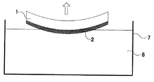
本発明の第1の実施形態に係る透明基材は、例えば、図1に示すように、表面の少なくとも一部に屈曲面を有する基材1と、基材1の屈曲面上に設けられた防眩層2を有する。以下、図1を使用して本発明の第1の実施形態に係る透明基材を説明する。なお、基材において表面とは防眩層2が設けられた側の面のことであり、表面と裏面とは、その組成や状態が同じであっても異なっていてもよい。図1に示す透明基材にあっては、基材のうち凸面側が表面、凹面側が裏面である。
屈曲部の曲率半径の下限値も特に制限はないが、1mm以上が好ましく、5mm以上がより好ましく、10mm以上がさらに好ましい。屈曲部の曲率半径が1mm以上であれば、屈曲面を有する基材の周辺部にある他部材と、滑らかに接続したデザインが得られやすい。
屈曲部の曲げ深さの下限値も特に制限はないが、3mm以上が好ましく、5mm以上がより好ましく、10mm以上がさらに好ましく、20mm以上が特に好ましい。屈曲部の曲げ深さが3mm以上であれば、屈曲部を有する基材の周辺部にある他部材と滑らかに接続したデザインが得られやすい。また屈曲面を有する基材の材質がガラスの場合、基材の剛性が向上し、組み付け工程時の変形抑制や、使用時の指での押し圧による不用意な変形を抑制できる。
なお、曲げ深さは、屈曲部を有する基材の厚さ方向断面視で、同一の主面における2つの端部を結ぶ直線と、この直線と平行となる直線のうち、屈曲部に接する接線との距離をいう。
ガラス組成がSiO2を60モル%以上、かつAl2O3を8モル%以上含有するアルミノシリケートガラスであると、さらに大きな表面圧縮応力および圧縮応力層深さを実現できるため、安全性が重視される車載用のディスプレイのカバーガラスに好適である。ガラスを用いる場合には基材1の厚さは0.5〜3mm程度である。
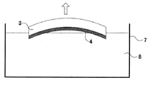
本発明の第2の実施形態に係る透明基材は、例えば、図2に示すように、屈曲面を表面に有する基材3と、基材3の屈曲面上に設けられた防眩層4を有する。以下、図2を使用して本発明の第2の実施形態に係る透明基材を説明する。
本発明の第3の実施形態に係る透明基材は、例えば、図3に示すように、複数の屈曲面を表面に有する基材5と、基材5の屈曲面上に設けられた防眩層6を有する。以下、図3を使用して本発明の第3の実施形態に係る透明基材を説明する。
(第1の実施形態)
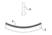
図4は本発明の第1の実施形態に係る透明基材の製造方法の一形態を模式的に示した断面図である。以下、図4を使用して本発明の第1の実施形態に係る透明基材の製造方法の一例を説明する。
図6は本発明の第2の実施形態に係る透明基材の製造方法の一形態を模式的に示した断面図である。以下、図6を使用して本発明の第2の実施形態に係る透明基材の製造方法の一例を説明する。
本実施形態の透明基材の製造方法は前記した第1および第2の実施形態を組み合わせて実施可能であるため詳細な説明は省略する。
以上説明したように、本発明は上記の実施形態に限定されるものではなく、実施形態の各構成を相互に組み合わせることや、明細書の記載、並びに周知の技術に基づいて、当業者が変更、応用することも本発明の予定するところであり、保護を求める範囲に含まれる。
例えば、基材や透明基材(以下、被加工物と記載)には以下のような工程・処理がされてもよい。
被加工物の端面は、面取加工等の処理がなされていてもよい。機械的な研削により一般的にR面取、C面取と呼ばれる加工を実施するのが好ましいが、エッチング等で加工を行ってもよく、特に限定されない。また、平板状の被成形ガラスを予め端面加工してから成形工程を経て屈曲部を有する基材としてもよい。
また成形工程前後問わず、被加工物に孔あけ加工や切断工程を行ってもよい。
被加工物がガラスである場合、該被加工物に表面圧縮応力層を形成する強化処理方法として、物理強化法や化学強化法が利用できる。ガラス主面が強化処理された被加工物は、機械的強度が高くなる。本構成においては、いずれの強化手法を採用してもよいが、厚みが薄くかつ表面圧縮応力(CS)値が大きな被加工物を得る場合には、化学強化法によって強化するのが好ましい。
強化処理工程は、成形工程後に実施することが好ましい。
被加工物に、化学強化により表面に圧縮応力層を形成し、強度及び耐擦傷性を高められる。化学強化は、ガラス転移点以下の温度でイオン交換によりガラス表面のイオン半径が小さなアルカリ金属イオン(典型的には、Liイオン、Naイオン)を、イオン半径のより大きなアルカリ金属イオン(典型的には、Liイオンに対してはNaイオン、Naイオンに対してはKイオン)に交換することで、ガラス表面に圧縮応力層を形成する処理である。化学強化処理は従来公知の方法によって実施でき、一般的には硝酸カリウム溶融塩にガラスを浸漬する。この溶融塩に炭酸カリウムを10質量%以下入れて使用してもよい。これによりガラスの表層のクラックなどを除去でき高強度のガラスを得られる。他に硝酸ナトリウムなどを混合した硝酸カリウム混合塩を使用してもよく、硝酸カリウム溶融塩中に水蒸気や炭酸ガスなどを吹き込んでもよい。化学強化時に硝酸カリウムに硝酸銀などの銀成分を混合することで、ガラスがイオン交換され銀イオンを表面に有し、抗菌性が付与される。
基材の裏面の少なくとも一部に印刷層を有することも好ましい。印刷層は、用途に応じて種々の印刷方法、インキ(印刷材料)により形成されて良い。印刷方法としては、例えば、スプレー印刷、インクジェット印刷やスクリーン印刷を利用できる。これらの方法により、面積の広い被加工物でも良好に印刷できる。特に、スプレー印刷では、屈曲部を有する被加工物に印刷しやすく、印刷面の表面粗さを調整しやすい。一方、スクリーン印刷では、広い被加工物に平均厚さが均一になるように所望の印刷パターンを形成しやすい。また、インキは、複数使用してよいが、印刷層の密着性の観点から同一のインキであるのが好ましい。印刷層を形成するインキは、無機系でも有機系であってもよい。
例1〜3のうち、例1および例2は実施例であり、例3は比較例である。
各例で使用した評価方法および材料を以下に示す。
「60゜鏡面光沢度」は、JIS Z8741:1997の60゜鏡面光沢度に規定されている方法で、光沢度計(コニカミノルタ社製、MULTI GLOSS 268Plus)を用い、防眩層付き基材の裏面反射は消さず測定した。
「ヘイズ」は、JIS K7136:2000(ISO14782:1999)に記載された方法によって測定され、ヘイズメーター(村上色彩研究所社製、HR−100型)を用いて測定した。
「算術平均粗さRa」は、JIS B0601:2001(ISO4287:1997)に記載された方法によって測定し、表面粗さ測定機(東京精密社製、サーフコム130A)を用いて測定した。測定長さは4mmとした。
[使用材料]
(鱗片状シリカ粒子分散液(a)の製造)
特開2014−094845号公報に記載された実施例1と同様の工程により、シリカ分散体を作製後、酸処理して洗浄、アルカリ処理、湿式解砕し、最後にカチオン交換したシリカ分散体を作製した。カチオン交換後のシリカ分散体を限外濾過膜(ダイセンメンブレンシステム製、MOLSEP(登録商標)、分画分子量:150000)にて処理し、濃度調整した。
得られたシリカ分散体(鱗片状シリカ粒子分散液(a))からシリカ粒子を取り出し、TEMにて観察したところ、不定形シリカ粒子を実質的に含まない鱗片状シリカ粒子のみであることが確認された。
鱗片状シリカ粒子分散液(a)に含まれる鱗片状シリカ粒子の平均粒子径は、湿式解砕後と同じであり、0.182μmであった。平均アスペクト比は188であった。
赤外線水分計で計測した鱗片状シリカ粒子分散液(a)の固形分濃度は5.0質量%であった。
変性エタノール(日本アルコール販売社製、ソルミックス(登録商標)AP−11、エタノールを主剤とした混合溶媒、沸点78℃。以下同じ。)の34.3gを撹拌しながら、シリケート40(多摩化学工業社製、テトラエトキシシランおよびその加水分解縮合物の混合物、固形分濃度(SiO2換算):40質量%、溶媒:エタノール(10%以下)。以下同じ。)の4.2gおよび鱗片状シリカ粒子分散液(a)の2.0gを加え、30分間撹拌した。これに、イオン交換水の3.6gおよび硝酸水溶液(硝酸濃度:61質量%)の0.06gの混合液を加え、60分間撹拌し、固形分濃度(SiO2換算)が4.0質量%のベース液(b)を調製した。なお、SiO2換算固形分濃度は、シリケート40のすべてのSiがSiO2に転化したときの固形分濃度である。
変性エタノールの3.85gを撹拌しながら、イオン交換水の0.4gおよび硝酸水溶液(硝酸濃度:61質量%)の0.01gの混合液を加え、5分間撹拌した。次いで、1,6−ビス(トリメトキシシリル)ヘキサン(信越化学工業社製、KBM−3066、固形分濃度(SiO2換算):37質量%)の0.5gを加え、ウォーターバス中60℃で15分間撹拌し、固形分濃度(SiO2換算)が4.3質量%のシラン化合物溶液(c)を調製した。
ベース液(b)の44.1gを撹拌しながら、シラン化合物溶液(c)の4.8gを加え、60分間撹拌した。これに、変性エタノールの146.7gを加え、室温で30分間撹拌し、固形分濃度(SiO2換算)が1.0質量%の組成物(d)を得た。
曲げ基材として、図7に示すような屈曲部と平坦部を備えた形状のアルミノシリケートガラス(ドラゴントレイル(商品名);旭硝子社製、サイズ:x=500mm、y=200mm(曲げ深さh=65mm)、厚さt=1.1mmのガラス基板。)を用意した。前記曲げ基材について化学強化処理を行い、CS750MPa、圧縮応力層深さ(DOL)28μmの圧縮応力層を形成した。該ガラスの表面を酸化セリウム分散水で洗浄後、イオン交換水でリンスし、乾燥させた。なお、使用した曲げ基材を上に凸になるように平坦面に載置し、平坦面との接地点を高さ0%、平坦面と最も遠い距離にある点を高さ100%とした場合、中央領域とは90〜100%の高さの58.5〜65mmの領域であり、端部領域とは0〜10%の高さの0〜6.5mmの領域である。
静電塗装装置(液体静電コーター、旭サナック社製)を用意し、静電塗装ガンとしては、回転霧化式自動静電ガン(旭サナック社製、サンベル、ESA120、70φカップ)を用意した。
基材を載置するための導電性基板として、カーボン製の導電性基板を用意した。これら導電性基板は成膜を行う曲げ基材との接触面と一致する形状となるように加工した。
(例1)
静電塗装装置のコーティングブース内の温度を25±1℃、湿度を50%±10%に調節した。
静電塗装装置のチェーンコンベア上に、カーボン製の導電性基板を介して曲げ基材を置いた。チェーンコンベアで等速搬送しながら、曲げ基材のトップ面(フロート法による製造時に溶融スズに接した面の反対側の面)に、表1に示す塗布条件による静電塗装法によって組成物(d)を塗布した後、大気中、300℃で60分間焼成し、防眩膜付き曲げ基材を得た。なお、防眩膜中のシリカ含有量は90%以上であった。
コート回数以外は例1と同様の条件で静電塗装を行った。例1および例2の塗布条件について表1に示す。例1、例2ともに凹面側に成膜を行った。

例3は例1および例2とは異なり、スプレー法により凹面側に成膜した。
[使用材料]
VAUノズルのエア吐出圧を0.4MPaに設定し、洗浄済みの曲げ基材上を750mm/分の速度で横方向に移動し、次いで、前方へ22mm移動し、そこから曲げ基材上を750mm/分のスピードで横方向に移動する。このとき、ガラスとVAUノズルの距離は200mmで一定となるように走査した。VAUノズルの移動は、あらかじめ90℃±3℃に加熱しておいた洗浄済みの曲げ基材の全面をVAUノズルがスキャニングするまで実施する。この方法で基材の全面に組成物を塗布したものを1面コート品と呼ぶ。その上に、さらに同じ方法でもう1回組成物を塗布することも出来る。同様に塗り重ねしていくことで、3面以上のコート品が得られる。表2に示す塗布条件によって組成物(d)を塗布した後、大気中、300℃で60分間焼成し、防眩膜付き曲げ基材を得た。
例1〜3の透明基材について、60°鏡面光沢度および表面粗さRaついての評価を行った。結果を表3に示す。例1および例2の透明基材は、屈曲面の中央領域(平坦面からの高さ61mmおよび62mmが相当)と端部領域(平坦面からの高さ4mmが相当)との60°鏡面光沢度の差の絶対値が20%超であった。また、欠点なども観察されず美観に優れた防眩膜であった。一方、例3の透明基材は、平坦部も屈曲部も同等の60°鏡面光沢度となる防眩膜が成膜された。
2、4、6 防眩層
7 処理槽
8 処理液
9 ノズル
Claims (19)
- 表面の少なくとも一部に屈曲面を有する基材と、
前記屈曲面の中央領域および端部領域上に設けられた防眩層とを備え、
前記中央領域の60°鏡面光沢度と、前記端部領域の60°鏡面光沢度との差の絶対値が20%超であることを特徴とする透明基材。 - 前記中央領域の60°鏡面光沢度が、前記端部領域の60°鏡面光沢度よりも小さい、請求項1に記載の透明基材。
- 前記中央領域の60°鏡面光沢度が30%以上120%未満であり、かつ前記端部領域の60°鏡面光沢度が60%〜140%である、請求項2に記載の透明基材。
- 前記中央領域の60°鏡面光沢度が80%以上120%未満であり、かつ前記端部領域の60°鏡面光沢度が100%〜140%である、請求項3に記載の透明基材。
- 前記防眩層は、前記屈曲面の中央領域から屈曲方向端部領域に向かって表面粗さRaが小さくなる、請求項4に記載の透明基材。
- 前記中央領域の60°鏡面光沢度が、前記端部領域の60°鏡面光沢度よりも大きい、請求項1に記載の透明基材。
- 前記端部領域の60°鏡面光沢度が30%以上120%未満であり、かつ前記中央領域の60°鏡面光沢度が60%〜140%である、請求項6に記載の透明基材。
- 前記端部領域の60°鏡面光沢度が80%以上120%未満であり、かつ前記中央領域の60°鏡面光沢度が100%〜140%である、請求項7に記載の透明基材。
- 前記防眩層は、前記屈曲面の中央領域から屈曲方向端部領域に向かって表面粗さRaが大きくなる、請求項8に記載の透明基材。
- 前記防眩層は、前記基材の表面の少なくとも一部がエッチングされた粗面化層である、請求項1〜9のいずれか1項に記載の透明基材。
- 前記防眩層は、前記基材の表面上の少なくとも一部に成膜された、シリカを主成分とする層である、請求項1〜9のいずれか1項に記載の透明基材。
- 前記基材が複数の屈曲面を有する、請求項1に記載の透明基材。
- 前記基材がガラスである、請求項1〜12のいずれか一項に記載の透明基材。
- 前記ガラスの表面には圧縮応力層がある、請求項13に記載の透明基材。
- 前記基材の裏面の少なくとも一部に印刷層を有する、請求項1〜14のいずれか一項に記載の透明基材。
- 請求項1〜15のいずれか一項に記載の透明基材からなるカバーガラスとディスプレイとを備える表示装置。
- 車載用である、請求項16に記載の表示装置。
- 表面の少なくとも一部に屈曲面を有する基材を用意する工程と、
前記基材を処理液に浸漬する工程と、
浸漬後、前記屈曲面内で60°鏡面光沢度が最大である領域と最小である領域における60°鏡面光沢度の差の絶対値が20%超となるように前記基材を前記処理液から取り出す工程とを備えることを特徴とする透明基材の製造方法。 - 表面の少なくとも一部に屈曲面を有する基材を用意する工程と、
前記基材の屈曲面上にノズルを位置させる工程と、
前記ノズルからケイ素を含む塗布液を吐出し、前記基材上に塗膜を形成する工程と、
前記塗膜を焼成する工程とを備え、
前記ノズルの吐出口の面積が、前記ノズルの方向から見たときの前記基材の面積の20%以下であることを特徴とする透明基材の製造方法。
Applications Claiming Priority (2)
| Application Number | Priority Date | Filing Date | Title |
|---|---|---|---|
| JP2016148399 | 2016-07-28 | ||
| JP2016148399 | 2016-07-28 |
Publications (2)
| Publication Number | Publication Date |
|---|---|
| JP2018024240A true JP2018024240A (ja) | 2018-02-15 |
| JP6855967B2 JP6855967B2 (ja) | 2021-04-07 |
Family
ID=61010639
Family Applications (1)
| Application Number | Title | Priority Date | Filing Date |
|---|---|---|---|
| JP2017140284A Active JP6855967B2 (ja) | 2016-07-28 | 2017-07-19 | 透明基材およびその製造方法 |
Country Status (2)
| Country | Link |
|---|---|
| US (2) | US10211237B2 (ja) |
| JP (1) | JP6855967B2 (ja) |
Cited By (4)
| Publication number | Priority date | Publication date | Assignee | Title |
|---|---|---|---|---|
| WO2019240178A1 (ja) * | 2018-06-13 | 2019-12-19 | 日本板硝子株式会社 | 防眩膜付基材、画像表示装置、及びデジタルサイネージ |
| JP2021533414A (ja) * | 2018-08-08 | 2021-12-02 | エージーシー グラス ユーロップAgc Glass Europe | 表示装置 |
| WO2023095538A1 (ja) * | 2021-11-26 | 2023-06-01 | 日本板硝子株式会社 | カバー部材 |
| US11994650B2 (en) | 2018-06-13 | 2024-05-28 | Nippon Sheet Glass Company, Limited | Antiglare film-attached substrate, image display apparatus, and digital signage |
Families Citing this family (10)
| Publication number | Priority date | Publication date | Assignee | Title |
|---|---|---|---|---|
| KR101920395B1 (ko) * | 2017-01-23 | 2018-11-20 | 주식회사 가치소프트 | 자동 물품 싱귤레이터 및 그 방법 |
| US20220011572A1 (en) * | 2018-11-29 | 2022-01-13 | Corning Incorporated | Aspheric mirror with reverse curvature for head-up display system and methods for forming the same |
| CN109920938B (zh) * | 2019-03-26 | 2021-03-19 | 京东方科技集团股份有限公司 | Oled显示面板及oled显示装置 |
| CN114097016B (zh) * | 2019-07-10 | 2023-10-20 | Agc株式会社 | 玻璃基体、盖板玻璃、组装体以及组装体的制造方法 |
| EP4071789A4 (en) | 2019-09-19 | 2024-02-14 | Lg Electronics Inc | SUBSTRATE CHUCK FOR SELF-ASSEMBLY OF LIGHT-EMITTING SEMICONDUCTOR DIODES |
| WO2021054507A1 (ko) | 2019-09-19 | 2021-03-25 | 엘지전자 주식회사 | 반도체 발광소자의 자가조립 장치 |
| WO2021054548A1 (en) | 2019-09-19 | 2021-03-25 | Lg Electronics Inc. | Substrate chuck for self-assembling semiconductor light-emitting diodes |
| WO2021054508A1 (ko) | 2019-09-19 | 2021-03-25 | 엘지전자 주식회사 | 반도체 발광소자의 자가조립 장치 |
| WO2021054550A1 (en) * | 2019-09-19 | 2021-03-25 | Lg Electronics Inc. | Device for self-assembling semiconductor light-emitting diodes |
| KR102323256B1 (ko) | 2019-09-19 | 2021-11-08 | 엘지전자 주식회사 | 반도체 발광소자의 자가조립 장치 |
Citations (6)
| Publication number | Priority date | Publication date | Assignee | Title |
|---|---|---|---|---|
| JP2003202813A (ja) * | 2000-11-09 | 2003-07-18 | Matsushita Electric Ind Co Ltd | 画像表示装置用フェースパネルの表面処理方法、およびこの表面処理を施されたフェースパネルを備えた画像表示装置 |
| WO2014061614A1 (ja) * | 2012-10-17 | 2014-04-24 | 旭硝子株式会社 | 反射防止性を有するガラスの製造方法 |
| WO2015133346A1 (ja) * | 2014-03-03 | 2015-09-11 | 日本電気硝子株式会社 | アンチグレア膜付ガラス曲板の製造方法 |
| WO2015137196A1 (ja) * | 2014-03-14 | 2015-09-17 | 日本電気硝子株式会社 | ディスプレイのカバー部材及びその製造方法 |
| WO2015186669A1 (ja) * | 2014-06-02 | 2015-12-10 | 旭硝子株式会社 | 防眩膜付き基材、その製造方法、および物品 |
| JP2016018068A (ja) * | 2014-07-08 | 2016-02-01 | 旭硝子株式会社 | 防眩膜付き基材および物品 |
Family Cites Families (5)
| Publication number | Priority date | Publication date | Assignee | Title |
|---|---|---|---|---|
| US5221424A (en) * | 1991-11-21 | 1993-06-22 | Applied Materials, Inc. | Method for removal of photoresist over metal which also removes or inactivates corosion-forming materials remaining from previous metal etch |
| SG99350A1 (en) * | 2000-02-17 | 2003-10-27 | Hoya Corp | Glass for cathode-ray tube, strengthened glass, method for the production thereof and use thereof |
| TW522437B (en) * | 2000-11-09 | 2003-03-01 | Matsushita Electric Ind Co Ltd | Method of treating surface of face panel used for image display device, and image display device comprising the treated face panel |
| JP4893539B2 (ja) | 2007-08-30 | 2012-03-07 | 旭硝子株式会社 | アンチグレア層を有する物品およびその製造方法 |
| KR102320143B1 (ko) * | 2015-02-13 | 2021-11-02 | 삼성디스플레이 주식회사 | 표시장치 |
-
2017
- 2017-07-19 US US15/653,760 patent/US10211237B2/en active Active
- 2017-07-19 JP JP2017140284A patent/JP6855967B2/ja active Active
-
2019
- 2019-01-02 US US16/238,361 patent/US10741725B2/en active Active
Patent Citations (11)
| Publication number | Priority date | Publication date | Assignee | Title |
|---|---|---|---|---|
| JP2003202813A (ja) * | 2000-11-09 | 2003-07-18 | Matsushita Electric Ind Co Ltd | 画像表示装置用フェースパネルの表面処理方法、およびこの表面処理を施されたフェースパネルを備えた画像表示装置 |
| WO2014061614A1 (ja) * | 2012-10-17 | 2014-04-24 | 旭硝子株式会社 | 反射防止性を有するガラスの製造方法 |
| JP2016001201A (ja) * | 2012-10-17 | 2016-01-07 | 旭硝子株式会社 | 反射防止性を有するガラスの製造方法 |
| WO2015133346A1 (ja) * | 2014-03-03 | 2015-09-11 | 日本電気硝子株式会社 | アンチグレア膜付ガラス曲板の製造方法 |
| WO2015137196A1 (ja) * | 2014-03-14 | 2015-09-17 | 日本電気硝子株式会社 | ディスプレイのカバー部材及びその製造方法 |
| CN106415333A (zh) * | 2014-03-14 | 2017-02-15 | 日本电气硝子株式会社 | 显示器的罩部件及其制造方法 |
| WO2015186669A1 (ja) * | 2014-06-02 | 2015-12-10 | 旭硝子株式会社 | 防眩膜付き基材、その製造方法、および物品 |
| US20170021383A1 (en) * | 2014-06-02 | 2017-01-26 | Asahi Glss Company, Limited | Antiglare film-coated substrate, method for its production, and article |
| CN106457303A (zh) * | 2014-06-02 | 2017-02-22 | 旭硝子株式会社 | 带防眩膜的基材、其制造方法及物品 |
| JP2016018068A (ja) * | 2014-07-08 | 2016-02-01 | 旭硝子株式会社 | 防眩膜付き基材および物品 |
| CN105319616A (zh) * | 2014-07-08 | 2016-02-10 | 旭硝子株式会社 | 带防眩膜基材以及物品 |
Cited By (5)
| Publication number | Priority date | Publication date | Assignee | Title |
|---|---|---|---|---|
| WO2019240178A1 (ja) * | 2018-06-13 | 2019-12-19 | 日本板硝子株式会社 | 防眩膜付基材、画像表示装置、及びデジタルサイネージ |
| JP2019215448A (ja) * | 2018-06-13 | 2019-12-19 | 日本板硝子株式会社 | 防眩膜付基材、画像表示装置、及びデジタルサイネージ |
| US11994650B2 (en) | 2018-06-13 | 2024-05-28 | Nippon Sheet Glass Company, Limited | Antiglare film-attached substrate, image display apparatus, and digital signage |
| JP2021533414A (ja) * | 2018-08-08 | 2021-12-02 | エージーシー グラス ユーロップAgc Glass Europe | 表示装置 |
| WO2023095538A1 (ja) * | 2021-11-26 | 2023-06-01 | 日本板硝子株式会社 | カバー部材 |
Also Published As
| Publication number | Publication date |
|---|---|
| US20180033986A1 (en) | 2018-02-01 |
| JP6855967B2 (ja) | 2021-04-07 |
| US10741725B2 (en) | 2020-08-11 |
| US10211237B2 (en) | 2019-02-19 |
| US20190139996A1 (en) | 2019-05-09 |
Similar Documents
| Publication | Publication Date | Title |
|---|---|---|
| JP6855967B2 (ja) | 透明基材およびその製造方法 | |
| CN107443948B (zh) | 带有印刷层的板及显示装置 | |
| JP7201370B2 (ja) | 膜付き曲げ基材およびその製造方法、ならびに画像表示装置 | |
| US10948633B2 (en) | Translucent structure, method for manufacturing same, and article | |
| CN107924003B (zh) | 透光性结构体 | |
| US10802318B2 (en) | Transparent substrate with antifouling film and capacitance in-cell touch panel-type liquid crystal display device | |
| EP3179280B1 (en) | Translucent structure | |
| WO2015186753A1 (ja) | 機能膜付き化学強化ガラス板、その製造方法および物品 | |
| JP4893539B2 (ja) | アンチグレア層を有する物品およびその製造方法 | |
| CN108623179A (zh) | 防眩光玻璃基板 | |
| WO2015115492A1 (ja) | 太陽電池用防眩機能付きガラス板 | |
| WO2015163330A1 (ja) | アンチグレア層付き基材および物品 | |
| JP7414524B2 (ja) | 膜付きガラス基板、物品、および膜付きガラス基板の製造方法 | |
| CN211367395U (zh) | 玻璃构造体 | |
| US11590844B2 (en) | Glass substrate and in-vehicle display device | |
| CN115398282A (zh) | 带防眩膜的基材和带防眩膜的基材的制造方法 |
Legal Events
| Date | Code | Title | Description |
|---|---|---|---|
| A621 | Written request for application examination |
Free format text: JAPANESE INTERMEDIATE CODE: A621 Effective date: 20200206 |
|
| A977 | Report on retrieval |
Free format text: JAPANESE INTERMEDIATE CODE: A971007 Effective date: 20201111 |
|
| A131 | Notification of reasons for refusal |
Free format text: JAPANESE INTERMEDIATE CODE: A131 Effective date: 20201222 |
|
| A521 | Request for written amendment filed |
Free format text: JAPANESE INTERMEDIATE CODE: A523 Effective date: 20210120 |
|
| TRDD | Decision of grant or rejection written | ||
| A01 | Written decision to grant a patent or to grant a registration (utility model) |
Free format text: JAPANESE INTERMEDIATE CODE: A01 Effective date: 20210216 |
|
| A61 | First payment of annual fees (during grant procedure) |
Free format text: JAPANESE INTERMEDIATE CODE: A61 Effective date: 20210301 |
|
| R150 | Certificate of patent or registration of utility model |
Ref document number: 6855967 Country of ref document: JP Free format text: JAPANESE INTERMEDIATE CODE: R150 |
|
| R250 | Receipt of annual fees |
Free format text: JAPANESE INTERMEDIATE CODE: R250 |