JP2018014469A5 - - Google Patents
Download PDFInfo
- Publication number
- JP2018014469A5 JP2018014469A5 JP2016144764A JP2016144764A JP2018014469A5 JP 2018014469 A5 JP2018014469 A5 JP 2018014469A5 JP 2016144764 A JP2016144764 A JP 2016144764A JP 2016144764 A JP2016144764 A JP 2016144764A JP 2018014469 A5 JP2018014469 A5 JP 2018014469A5
- Authority
- JP
- Japan
- Prior art keywords
- moving body
- mounting table
- mounting
- substrate
- stages
- Prior art date
- Legal status (The legal status is an assumption and is not a legal conclusion. Google has not performed a legal analysis and makes no representation as to the accuracy of the status listed.)
- Granted
Links
- 235000012431 wafers Nutrition 0.000 description 10
- 239000000758 substrate Substances 0.000 description 8
- 230000000875 corresponding Effects 0.000 description 3
- 230000003028 elevating Effects 0.000 description 3
Images
Description
左右の各載置台62A、62Bは夫々4段配列されているが、この構成は一例に過ぎず、例えば7段の配列とし、左側の載置台62Aに、左側の前後に配置された処理ユニットUの各々に受け渡すために6枚の未処理ウエハWを搭載し、また右側の載置台62Bに、右側の前後に配置された処理ユニットUの各々に受け渡すために6枚の未処理ウエハWを搭載する運用であってもよい。
第2の実施形態のように、基板載置部3として左右に夫々複数段の載置台62A、62Bを設ける構成とすれば、第1の実施形態のように回転機構を用いなくとも、ロードロック室42内の基板搬送機構43が短いストロークでウエハWの受け渡しをできる利点がある。
Each of the left and right mounting tables 62A and 62B is arranged in four stages, but this configuration is merely an example. For example, the arrangement is a seven-stage arrangement, and the left mounting table 62A has processing units U arranged on the left and right sides. Six unprocessed wafers W are mounted for transfer to each of the wafers, and six unprocessed wafers W for transfer to each of the processing units U disposed at the front and rear of the right side on the right mounting table 62B. It may be an operation to install.
As in the second embodiment, if the substrate mounting section 3 is provided with a plurality of stages of mounting tables 62A and 62B on the left and right sides, a load lock can be achieved without using a rotating mechanism as in the first embodiment. There is an advantage that the substrate transfer mechanism 43 in the chamber 42 can deliver the wafer W with a short stroke.
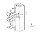
X移動体73には、第2の実施形態で用いられた載置台62A(62B)と同じ構造の載置台74が例えば7段設けられている。この例においては、7段の載置台74のうち例えば最上段の載置台74については空きスペースとし、受け渡し機構12により2段目以降の載置台74に未処理ウエハWを合計6枚搭載する。そして支柱部22を手前側の処理ユニットUに対応する位置まで移動させると共に昇降基体71により基板載置部3を最上段の処理ユニットUに対応する位置まで上昇する。
The X moving body 73 is provided with, for example, seven stages of mounting tables 74 having the same structure as the mounting tables 62A (62 B ) used in the second embodiment . In this example , for example, the top stage mounting table 74 among the seven stages mounting table 74 is set as an empty space, and a total of six unprocessed wafers W are mounted on the second and subsequent mounting tables 74 by the delivery mechanism 12. Then, the
そしてX移動体73を左側に寄ったところに位置させ、既に詳述したようにしてロードロック室42の基板搬送機構43により最上段の載置台74に処理済みウエハWを受け渡し、2段目の載置台74の未処理ウエハWを基板搬送機構43に受け渡す。次いで昇降基体71を載置台74の1段分上昇させると共にX移動体73を右側に寄ったところに位置させ、右側の最上段の処理ユニットU側から処理済みウエハWを2段目の載置台74に受け渡す。こうしてX移動体73を左右に順次移動させると共に昇降基体71の高さ位置を各処理ユニットUに対応する位置に設定することにより、基板載置部3と手前側の左右の処理ユニットUとの間で処理済みウエハWと未処理ウエハWとの受渡し(交換)が行われる。即ち、この例では、X移動体73が左側に寄った位置及び右側に寄った位置は、夫々第2の実施形態の載置台62A、62Bの位置に対応する。
この例においても基板搬送機構43のストロークが短くて済むが、X移動体73を構成する縦長の部材を左右の処理ユニットUの中間位置に固定する構成であってもよい。この構成であっても、基板搬送機構43のストロークが対応できる場合には、適用できる。
Then, the X moving body 73 is positioned on the left side, and the processed wafer W is delivered to the uppermost mounting table 74 by the substrate transfer mechanism 43 of the load lock chamber 42 as already described in detail. The unprocessed wafer W on the mounting table 74 is transferred to the substrate transfer mechanism 43. Next, the
In this example as well, the stroke of the substrate transport mechanism 43 may be short, but a vertically long member constituting the X moving body 73 may be fixed at an intermediate position between the left and right processing units U. Even this configuration can be applied if the stroke of the substrate transport mechanism 43 can be accommodated.
Priority Applications (5)
| Application Number | Priority Date | Filing Date | Title |
|---|---|---|---|
| JP2016144764A JP6747136B2 (en) | 2016-07-22 | 2016-07-22 | Substrate processing equipment |
| CN201780044348.2A CN109478527B (en) | 2016-07-22 | 2017-06-21 | Substrate processing apparatus |
| PCT/JP2017/022866 WO2018016257A1 (en) | 2016-07-22 | 2017-06-21 | Substrate processing device |
| KR1020197001350A KR102164404B1 (en) | 2016-07-22 | 2017-06-21 | Substrate processing equipment |
| US16/252,978 US10906756B2 (en) | 2016-07-22 | 2019-01-21 | Substrate processing device |
Applications Claiming Priority (1)
| Application Number | Priority Date | Filing Date | Title |
|---|---|---|---|
| JP2016144764A JP6747136B2 (en) | 2016-07-22 | 2016-07-22 | Substrate processing equipment |
Publications (3)
| Publication Number | Publication Date |
|---|---|
| JP2018014469A JP2018014469A (en) | 2018-01-25 |
| JP2018014469A5 true JP2018014469A5 (en) | 2019-11-07 |
| JP6747136B2 JP6747136B2 (en) | 2020-08-26 |
Family
ID=60992105
Family Applications (1)
| Application Number | Title | Priority Date | Filing Date |
|---|---|---|---|
| JP2016144764A Active JP6747136B2 (en) | 2016-07-22 | 2016-07-22 | Substrate processing equipment |
Country Status (5)
| Country | Link |
|---|---|
| US (1) | US10906756B2 (en) |
| JP (1) | JP6747136B2 (en) |
| KR (1) | KR102164404B1 (en) |
| CN (1) | CN109478527B (en) |
| WO (1) | WO2018016257A1 (en) |
Families Citing this family (5)
| Publication number | Priority date | Publication date | Assignee | Title |
|---|---|---|---|---|
| JP6851288B2 (en) * | 2017-08-23 | 2021-03-31 | 東京エレクトロン株式会社 | Substrate processing equipment and substrate transfer method |
| US11380564B2 (en) * | 2018-09-19 | 2022-07-05 | Applied Materials, Inc. | Processing system having a front opening unified pod (FOUP) load lock |
| JP7210960B2 (en) * | 2018-09-21 | 2023-01-24 | 東京エレクトロン株式会社 | Vacuum processing apparatus and substrate transfer method |
| KR20210127738A (en) * | 2019-03-19 | 2021-10-22 | 가부시키가이샤 코쿠사이 엘렉트릭 | Semiconductor device manufacturing method, substrate processing apparatus and program |
| US11705354B2 (en) * | 2020-07-10 | 2023-07-18 | Applied Materials, Inc. | Substrate handling systems |
Family Cites Families (14)
| Publication number | Priority date | Publication date | Assignee | Title |
|---|---|---|---|---|
| KR0147403B1 (en) * | 1994-06-24 | 1998-11-02 | 문정환 | Device of automatic chip loading |
| KR20020088419A (en) * | 2000-04-05 | 2002-11-27 | 동경 엘렉트론 주식회사 | Treating device |
| JP4114737B2 (en) * | 2001-03-09 | 2008-07-09 | 東京エレクトロン株式会社 | Processing equipment |
| JP2003188229A (en) | 2001-12-18 | 2003-07-04 | Hitachi Kasado Eng Co Ltd | System and method for manufacturing wafer |
| JP4389424B2 (en) * | 2001-12-25 | 2009-12-24 | 東京エレクトロン株式会社 | To-be-processed object conveyance mechanism and processing system |
| JP2004349503A (en) | 2003-05-22 | 2004-12-09 | Tokyo Electron Ltd | System and method for processing object to be processed |
| JP5264171B2 (en) * | 2004-06-09 | 2013-08-14 | ブルックス オートメーション インコーポレイテッド | Substrate transfer device |
| JP2008028035A (en) * | 2006-07-19 | 2008-02-07 | Phyzchemix Corp | Semiconductor-manufacturing apparatus |
| US7950407B2 (en) * | 2007-02-07 | 2011-05-31 | Applied Materials, Inc. | Apparatus for rapid filling of a processing volume |
| CN101330032B (en) * | 2008-07-22 | 2012-01-11 | 北京北方微电子基地设备工艺研究中心有限责任公司 | Plasma processing apparatus and transition chamber thereof |
| JP2011071293A (en) * | 2009-09-25 | 2011-04-07 | Tokyo Electron Ltd | Process module, substrate processing apparatus, and method of transferring substrate |
| KR102060544B1 (en) * | 2010-11-10 | 2019-12-30 | 브룩스 오토메이션 인코퍼레이티드 | Dual arm robot |
| KR102047033B1 (en) * | 2011-03-11 | 2019-11-20 | 브룩스 오토메이션 인코퍼레이티드 | Substrate processing tool |
| US9293317B2 (en) * | 2012-09-12 | 2016-03-22 | Lam Research Corporation | Method and system related to semiconductor processing equipment |
-
2016
- 2016-07-22 JP JP2016144764A patent/JP6747136B2/en active Active
-
2017
- 2017-06-21 CN CN201780044348.2A patent/CN109478527B/en active Active
- 2017-06-21 WO PCT/JP2017/022866 patent/WO2018016257A1/en active Application Filing
- 2017-06-21 KR KR1020197001350A patent/KR102164404B1/en active IP Right Grant
-
2019
- 2019-01-21 US US16/252,978 patent/US10906756B2/en active Active
Similar Documents
| Publication | Publication Date | Title |
|---|---|---|
| JP2018014469A5 (en) | ||
| JP2017108112A5 (en) | ||
| JP4980978B2 (en) | Substrate processing equipment | |
| TW200836289A (en) | Substrate transporting apparatus, substrate platform shelf and substrate processing apparatus | |
| JP2014513429A5 (en) | ||
| JP2010175565A (en) | Test handler | |
| JP2013143513A5 (en) | ||
| TWI265135B (en) | Substrate transporting device and substrate transfer method, and vacuum processing device | |
| KR102164404B1 (en) | Substrate processing equipment | |
| JP2011124564A5 (en) | Vacuum processing apparatus and operating method of vacuum processing apparatus | |
| JP2009004661A5 (en) | ||
| JP2012009870A5 (en) | ||
| JP2013102235A5 (en) | ||
| JP5518550B2 (en) | Object processing equipment | |
| JP5639963B2 (en) | Substrate processing apparatus, substrate processing method, and recording medium recording substrate processing program | |
| JP2017041523A5 (en) | ||
| JP2013058735A5 (en) | ||
| US10328580B2 (en) | Reduced footprint substrate transport vacuum platform | |
| WO2016185984A1 (en) | Treatment system | |
| US9214369B2 (en) | Dynamic pitch substrate lift | |
| KR20150090997A (en) | Feed mechanism | |
| JP2010041059A5 (en) | ||
| KR101024216B1 (en) | A unit and a method for transfering a wafer | |
| KR101383248B1 (en) | High speed substrate processing system | |
| JP2018060823A (en) | Carrier transport device and carrier transport method |