JP2018011073A - Solar battery module - Google Patents
Solar battery module Download PDFInfo
- Publication number
- JP2018011073A JP2018011073A JP2017172283A JP2017172283A JP2018011073A JP 2018011073 A JP2018011073 A JP 2018011073A JP 2017172283 A JP2017172283 A JP 2017172283A JP 2017172283 A JP2017172283 A JP 2017172283A JP 2018011073 A JP2018011073 A JP 2018011073A
- Authority
- JP
- Japan
- Prior art keywords
- connector
- solar cell
- wiring
- electrode
- cell module
- Prior art date
- Legal status (The legal status is an assumption and is not a legal conclusion. Google has not performed a legal analysis and makes no representation as to the accuracy of the status listed.)
- Granted
Links
- 239000000758 substrate Substances 0.000 claims abstract description 89
- 239000004065 semiconductor Substances 0.000 claims abstract description 74
- 239000000853 adhesive Substances 0.000 claims abstract description 35
- 230000001070 adhesive effect Effects 0.000 claims abstract description 35
- 238000009413 insulation Methods 0.000 abstract description 5
- 239000000463 material Substances 0.000 description 64
- 239000011248 coating agent Substances 0.000 description 20
- 238000000576 coating method Methods 0.000 description 20
- 239000007769 metal material Substances 0.000 description 19
- 239000010410 layer Substances 0.000 description 15
- 230000005684 electric field Effects 0.000 description 12
- 238000000034 method Methods 0.000 description 10
- 238000010586 diagram Methods 0.000 description 8
- 238000005452 bending Methods 0.000 description 6
- 239000010949 copper Substances 0.000 description 6
- 239000012792 core layer Substances 0.000 description 6
- 239000012535 impurity Substances 0.000 description 6
- 230000000644 propagated effect Effects 0.000 description 6
- 239000011247 coating layer Substances 0.000 description 5
- 238000005476 soldering Methods 0.000 description 5
- 238000002844 melting Methods 0.000 description 4
- 230000008018 melting Effects 0.000 description 4
- 239000002184 metal Substances 0.000 description 4
- 229910052751 metal Inorganic materials 0.000 description 4
- 238000010248 power generation Methods 0.000 description 4
- RYGMFSIKBFXOCR-UHFFFAOYSA-N Copper Chemical compound [Cu] RYGMFSIKBFXOCR-UHFFFAOYSA-N 0.000 description 3
- ATJFFYVFTNAWJD-UHFFFAOYSA-N Tin Chemical compound [Sn] ATJFFYVFTNAWJD-UHFFFAOYSA-N 0.000 description 3
- 229910052802 copper Inorganic materials 0.000 description 3
- 239000000945 filler Substances 0.000 description 3
- 238000004519 manufacturing process Methods 0.000 description 3
- 229910000679 solder Inorganic materials 0.000 description 3
- BQCADISMDOOEFD-UHFFFAOYSA-N Silver Chemical compound [Ag] BQCADISMDOOEFD-UHFFFAOYSA-N 0.000 description 2
- 230000000694 effects Effects 0.000 description 2
- 239000011810 insulating material Substances 0.000 description 2
- 239000002923 metal particle Substances 0.000 description 2
- 239000011347 resin Substances 0.000 description 2
- 229920005989 resin Polymers 0.000 description 2
- 229910052709 silver Inorganic materials 0.000 description 2
- 239000004332 silver Substances 0.000 description 2
- 239000000126 substance Substances 0.000 description 2
- 239000004593 Epoxy Substances 0.000 description 1
- XUIMIQQOPSSXEZ-UHFFFAOYSA-N Silicon Chemical compound [Si] XUIMIQQOPSSXEZ-UHFFFAOYSA-N 0.000 description 1
- 229910007637 SnAg Inorganic materials 0.000 description 1
- 229910008433 SnCU Inorganic materials 0.000 description 1
- 229910007116 SnPb Inorganic materials 0.000 description 1
- 239000002313 adhesive film Substances 0.000 description 1
- 229910045601 alloy Inorganic materials 0.000 description 1
- 239000000956 alloy Substances 0.000 description 1
- 229910052782 aluminium Inorganic materials 0.000 description 1
- 239000000470 constituent Substances 0.000 description 1
- 230000008602 contraction Effects 0.000 description 1
- 229910021419 crystalline silicon Inorganic materials 0.000 description 1
- 239000011521 glass Substances 0.000 description 1
- 229910052738 indium Inorganic materials 0.000 description 1
- APFVFJFRJDLVQX-UHFFFAOYSA-N indium atom Chemical compound [In] APFVFJFRJDLVQX-UHFFFAOYSA-N 0.000 description 1
- 239000011159 matrix material Substances 0.000 description 1
- 238000012986 modification Methods 0.000 description 1
- 230000004048 modification Effects 0.000 description 1
- 230000003287 optical effect Effects 0.000 description 1
- 238000002161 passivation Methods 0.000 description 1
- 230000000704 physical effect Effects 0.000 description 1
- 229920000642 polymer Polymers 0.000 description 1
- 238000005036 potential barrier Methods 0.000 description 1
- 238000005215 recombination Methods 0.000 description 1
- 230000006798 recombination Effects 0.000 description 1
- 238000000926 separation method Methods 0.000 description 1
- 229910052710 silicon Inorganic materials 0.000 description 1
- 239000010703 silicon Substances 0.000 description 1
- 239000002210 silicon-based material Substances 0.000 description 1
- 238000006467 substitution reaction Methods 0.000 description 1
Images


Classifications
-
- H—ELECTRICITY
- H01—ELECTRIC ELEMENTS
- H01L—SEMICONDUCTOR DEVICES NOT COVERED BY CLASS H10
- H01L31/00—Semiconductor devices sensitive to infrared radiation, light, electromagnetic radiation of shorter wavelength or corpuscular radiation and specially adapted either for the conversion of the energy of such radiation into electrical energy or for the control of electrical energy by such radiation; Processes or apparatus specially adapted for the manufacture or treatment thereof or of parts thereof; Details thereof
- H01L31/04—Semiconductor devices sensitive to infrared radiation, light, electromagnetic radiation of shorter wavelength or corpuscular radiation and specially adapted either for the conversion of the energy of such radiation into electrical energy or for the control of electrical energy by such radiation; Processes or apparatus specially adapted for the manufacture or treatment thereof or of parts thereof; Details thereof adapted as photovoltaic [PV] conversion devices
- H01L31/042—PV modules or arrays of single PV cells
- H01L31/05—Electrical interconnection means between PV cells inside the PV module, e.g. series connection of PV cells
- H01L31/0504—Electrical interconnection means between PV cells inside the PV module, e.g. series connection of PV cells specially adapted for series or parallel connection of solar cells in a module
- H01L31/0516—Electrical interconnection means between PV cells inside the PV module, e.g. series connection of PV cells specially adapted for series or parallel connection of solar cells in a module specially adapted for interconnection of back-contact solar cells
-
- H—ELECTRICITY
- H01—ELECTRIC ELEMENTS
- H01L—SEMICONDUCTOR DEVICES NOT COVERED BY CLASS H10
- H01L31/00—Semiconductor devices sensitive to infrared radiation, light, electromagnetic radiation of shorter wavelength or corpuscular radiation and specially adapted either for the conversion of the energy of such radiation into electrical energy or for the control of electrical energy by such radiation; Processes or apparatus specially adapted for the manufacture or treatment thereof or of parts thereof; Details thereof
- H01L31/04—Semiconductor devices sensitive to infrared radiation, light, electromagnetic radiation of shorter wavelength or corpuscular radiation and specially adapted either for the conversion of the energy of such radiation into electrical energy or for the control of electrical energy by such radiation; Processes or apparatus specially adapted for the manufacture or treatment thereof or of parts thereof; Details thereof adapted as photovoltaic [PV] conversion devices
- H01L31/042—PV modules or arrays of single PV cells
- H01L31/05—Electrical interconnection means between PV cells inside the PV module, e.g. series connection of PV cells
- H01L31/0504—Electrical interconnection means between PV cells inside the PV module, e.g. series connection of PV cells specially adapted for series or parallel connection of solar cells in a module
- H01L31/0512—Electrical interconnection means between PV cells inside the PV module, e.g. series connection of PV cells specially adapted for series or parallel connection of solar cells in a module made of a particular material or composition of materials
-
- H—ELECTRICITY
- H01—ELECTRIC ELEMENTS
- H01L—SEMICONDUCTOR DEVICES NOT COVERED BY CLASS H10
- H01L31/00—Semiconductor devices sensitive to infrared radiation, light, electromagnetic radiation of shorter wavelength or corpuscular radiation and specially adapted either for the conversion of the energy of such radiation into electrical energy or for the control of electrical energy by such radiation; Processes or apparatus specially adapted for the manufacture or treatment thereof or of parts thereof; Details thereof
- H01L31/02—Details
- H01L31/02002—Arrangements for conducting electric current to or from the device in operations
- H01L31/02005—Arrangements for conducting electric current to or from the device in operations for device characterised by at least one potential jump barrier or surface barrier
- H01L31/02008—Arrangements for conducting electric current to or from the device in operations for device characterised by at least one potential jump barrier or surface barrier for solar cells or solar cell modules
- H01L31/0201—Arrangements for conducting electric current to or from the device in operations for device characterised by at least one potential jump barrier or surface barrier for solar cells or solar cell modules comprising specially adapted module bus-bar structures
-
- H—ELECTRICITY
- H01—ELECTRIC ELEMENTS
- H01L—SEMICONDUCTOR DEVICES NOT COVERED BY CLASS H10
- H01L31/00—Semiconductor devices sensitive to infrared radiation, light, electromagnetic radiation of shorter wavelength or corpuscular radiation and specially adapted either for the conversion of the energy of such radiation into electrical energy or for the control of electrical energy by such radiation; Processes or apparatus specially adapted for the manufacture or treatment thereof or of parts thereof; Details thereof
- H01L31/02—Details
- H01L31/02016—Circuit arrangements of general character for the devices
- H01L31/02019—Circuit arrangements of general character for the devices for devices characterised by at least one potential jump barrier or surface barrier
- H01L31/02021—Circuit arrangements of general character for the devices for devices characterised by at least one potential jump barrier or surface barrier for solar cells
-
- H—ELECTRICITY
- H01—ELECTRIC ELEMENTS
- H01L—SEMICONDUCTOR DEVICES NOT COVERED BY CLASS H10
- H01L31/00—Semiconductor devices sensitive to infrared radiation, light, electromagnetic radiation of shorter wavelength or corpuscular radiation and specially adapted either for the conversion of the energy of such radiation into electrical energy or for the control of electrical energy by such radiation; Processes or apparatus specially adapted for the manufacture or treatment thereof or of parts thereof; Details thereof
- H01L31/02—Details
- H01L31/0224—Electrodes
- H01L31/022408—Electrodes for devices characterised by at least one potential jump barrier or surface barrier
- H01L31/022425—Electrodes for devices characterised by at least one potential jump barrier or surface barrier for solar cells
- H01L31/022441—Electrode arrangements specially adapted for back-contact solar cells
-
- H—ELECTRICITY
- H01—ELECTRIC ELEMENTS
- H01L—SEMICONDUCTOR DEVICES NOT COVERED BY CLASS H10
- H01L31/00—Semiconductor devices sensitive to infrared radiation, light, electromagnetic radiation of shorter wavelength or corpuscular radiation and specially adapted either for the conversion of the energy of such radiation into electrical energy or for the control of electrical energy by such radiation; Processes or apparatus specially adapted for the manufacture or treatment thereof or of parts thereof; Details thereof
- H01L31/04—Semiconductor devices sensitive to infrared radiation, light, electromagnetic radiation of shorter wavelength or corpuscular radiation and specially adapted either for the conversion of the energy of such radiation into electrical energy or for the control of electrical energy by such radiation; Processes or apparatus specially adapted for the manufacture or treatment thereof or of parts thereof; Details thereof adapted as photovoltaic [PV] conversion devices
- H01L31/042—PV modules or arrays of single PV cells
- H01L31/05—Electrical interconnection means between PV cells inside the PV module, e.g. series connection of PV cells
- H01L31/0504—Electrical interconnection means between PV cells inside the PV module, e.g. series connection of PV cells specially adapted for series or parallel connection of solar cells in a module
-
- H—ELECTRICITY
- H01—ELECTRIC ELEMENTS
- H01L—SEMICONDUCTOR DEVICES NOT COVERED BY CLASS H10
- H01L31/00—Semiconductor devices sensitive to infrared radiation, light, electromagnetic radiation of shorter wavelength or corpuscular radiation and specially adapted either for the conversion of the energy of such radiation into electrical energy or for the control of electrical energy by such radiation; Processes or apparatus specially adapted for the manufacture or treatment thereof or of parts thereof; Details thereof
- H01L31/04—Semiconductor devices sensitive to infrared radiation, light, electromagnetic radiation of shorter wavelength or corpuscular radiation and specially adapted either for the conversion of the energy of such radiation into electrical energy or for the control of electrical energy by such radiation; Processes or apparatus specially adapted for the manufacture or treatment thereof or of parts thereof; Details thereof adapted as photovoltaic [PV] conversion devices
- H01L31/06—Semiconductor devices sensitive to infrared radiation, light, electromagnetic radiation of shorter wavelength or corpuscular radiation and specially adapted either for the conversion of the energy of such radiation into electrical energy or for the control of electrical energy by such radiation; Processes or apparatus specially adapted for the manufacture or treatment thereof or of parts thereof; Details thereof adapted as photovoltaic [PV] conversion devices characterised by at least one potential-jump barrier or surface barrier
- H01L31/068—Semiconductor devices sensitive to infrared radiation, light, electromagnetic radiation of shorter wavelength or corpuscular radiation and specially adapted either for the conversion of the energy of such radiation into electrical energy or for the control of electrical energy by such radiation; Processes or apparatus specially adapted for the manufacture or treatment thereof or of parts thereof; Details thereof adapted as photovoltaic [PV] conversion devices characterised by at least one potential-jump barrier or surface barrier the potential barriers being only of the PN homojunction type, e.g. bulk silicon PN homojunction solar cells or thin film polycrystalline silicon PN homojunction solar cells
- H01L31/0682—Semiconductor devices sensitive to infrared radiation, light, electromagnetic radiation of shorter wavelength or corpuscular radiation and specially adapted either for the conversion of the energy of such radiation into electrical energy or for the control of electrical energy by such radiation; Processes or apparatus specially adapted for the manufacture or treatment thereof or of parts thereof; Details thereof adapted as photovoltaic [PV] conversion devices characterised by at least one potential-jump barrier or surface barrier the potential barriers being only of the PN homojunction type, e.g. bulk silicon PN homojunction solar cells or thin film polycrystalline silicon PN homojunction solar cells back-junction, i.e. rearside emitter, solar cells, e.g. interdigitated base-emitter regions back-junction cells
-
- Y—GENERAL TAGGING OF NEW TECHNOLOGICAL DEVELOPMENTS; GENERAL TAGGING OF CROSS-SECTIONAL TECHNOLOGIES SPANNING OVER SEVERAL SECTIONS OF THE IPC; TECHNICAL SUBJECTS COVERED BY FORMER USPC CROSS-REFERENCE ART COLLECTIONS [XRACs] AND DIGESTS
- Y02—TECHNOLOGIES OR APPLICATIONS FOR MITIGATION OR ADAPTATION AGAINST CLIMATE CHANGE
- Y02E—REDUCTION OF GREENHOUSE GAS [GHG] EMISSIONS, RELATED TO ENERGY GENERATION, TRANSMISSION OR DISTRIBUTION
- Y02E10/00—Energy generation through renewable energy sources
- Y02E10/50—Photovoltaic [PV] energy
- Y02E10/52—PV systems with concentrators
-
- Y—GENERAL TAGGING OF NEW TECHNOLOGICAL DEVELOPMENTS; GENERAL TAGGING OF CROSS-SECTIONAL TECHNOLOGIES SPANNING OVER SEVERAL SECTIONS OF THE IPC; TECHNICAL SUBJECTS COVERED BY FORMER USPC CROSS-REFERENCE ART COLLECTIONS [XRACs] AND DIGESTS
- Y02—TECHNOLOGIES OR APPLICATIONS FOR MITIGATION OR ADAPTATION AGAINST CLIMATE CHANGE
- Y02E—REDUCTION OF GREENHOUSE GAS [GHG] EMISSIONS, RELATED TO ENERGY GENERATION, TRANSMISSION OR DISTRIBUTION
- Y02E10/00—Energy generation through renewable energy sources
- Y02E10/50—Photovoltaic [PV] energy
- Y02E10/547—Monocrystalline silicon PV cells
Abstract
Description
本発明は太陽電池モジュールに関する。 The present invention relates to a solar cell module.
一般的な太陽電池は、p型とn型のように、互いに異なる導電型(conductive type)の半導体からなる基板(substrate)とエミッタ部(emitter region)、そして基板とエミッタ部にそれぞれ接続された電極を備える。この時、基板とエミッタ部の界面にはp−n接合が形成されている。 A general solar cell is connected to a substrate and an emitter region made of semiconductors of different conductive types, such as p-type and n-type, and to the substrate and the emitter, respectively. With electrodes. At this time, a pn junction is formed at the interface between the substrate and the emitter.
このように、半導体基板を用いる太陽電池は、構造に応じて、コンベンショナルタイプ、後面コンタクトタイプなど様々な種類に分けられる。 Thus, solar cells using a semiconductor substrate are classified into various types such as a conventional type and a rear contact type according to the structure.
ここで、コンベンショナルタイプはエミッタ部が基板の前面に位置し、エミッタ部に接続された電極が基板の前面に、基板に接続される電極が基板の後面に位置し、後面コンタクトタイプはエミッタ部が基板の後面に位置し、電極がすべて基板の後面に位置する。 Here, in the conventional type, the emitter portion is located on the front surface of the substrate, the electrode connected to the emitter portion is located on the front surface of the substrate, the electrode connected to the substrate is located on the rear surface of the substrate, and the rear contact type is located on the emitter portion. Located on the rear surface of the substrate, all the electrodes are located on the rear surface of the substrate.
ここで、後面コンタクトタイプの太陽電池は、電極がすべて基板の後面に形成されるので、基板の後面に形成された電極をインターコネクタや別の導電性金属を介して隣接する太陽電池の電極に直列接続して太陽電池モジュールを形成することがある。 Here, since all the electrodes of the rear contact type solar cell are formed on the rear surface of the substrate, the electrode formed on the rear surface of the substrate is connected to the electrode of the adjacent solar cell via an interconnector or another conductive metal. Sometimes connected in series to form a solar cell module.
本発明の目的は、効率と構造的安定性がさらに向上した太陽電池モジュールを提供することにある。 An object of the present invention is to provide a solar cell module with further improved efficiency and structural stability.
本発明の一例に係る太陽電池モジュールは、半導体基板と、半導体基板に形成され、異なる導電性電荷を収集する第1電極と第2電極を含む複数の太陽電池と、複数の太陽電池の内で互いに隣接した第1太陽電池と第2太陽電池の第1電極と第2電極に接続される複数の配線であって、第1太陽電池と第2太陽電池の直列接続のために導電性接着剤で接続し、第1太陽電池と第2太陽電池の第1電極と第2電極から絶縁層で絶縁される複数の配線と、第1太陽電池と第2太陽電池間に位置して複数の配線に接続されているコネクタを含み、コネクタの幅は、第1太陽電池とコネクタの間の第1距離または第2太陽電池とコネクタとの間の第2距離の内の少なくとも一つと同じか大きく、コネクタ上の絶縁層の塗布面積は、コネクタ上の導電性接着剤の塗布面積より大きい。 A solar cell module according to an example of the present invention includes a semiconductor substrate, a plurality of solar cells formed on the semiconductor substrate and including first and second electrodes that collect different conductive charges, and a plurality of solar cells. A plurality of wirings connected to the first and second electrodes of the first solar cell and the second solar cell adjacent to each other, wherein the conductive adhesive is used for series connection of the first solar cell and the second solar cell. A plurality of wires connected by the first solar cell and the first and second electrodes of the second solar cell and insulated by an insulating layer from the first electrode and the second electrode, and a plurality of wires located between the first solar cell and the second solar cell The width of the connector is equal to or greater than at least one of the first distance between the first solar cell and the connector or the second distance between the second solar cell and the connector; The insulation area on the connector is conductive on the connector. Larger than the area of application of Chakuzai.
ここで、複数の配線の先端とコネクタとの重畳領域は、コネクタの幅と同じか、小さいことがある。 Here, the overlapping area between the tips of the plurality of wires and the connector may be the same as or smaller than the width of the connector.
一例として、各配線の先端がコネクタとの重畳領域は、コネクタの幅×1/3と同じか、大きいことがある。 As an example, the overlapping region where the tip of each wiring is connected to the connector may be the same as or larger than the connector width × 1/3.
また、コネクタは、光が入射する第1面と第1面と反対の第2面を含み、複数の配線のすべては、コネクタの第2面に接続することがある。 The connector includes a first surface on which light is incident and a second surface opposite to the first surface, and all of the plurality of wirings may be connected to the second surface of the connector.
ここで、コネクタの第1面には、互いに傾斜面の角度が異なる複数の凹凸を含むことができ、コネクタの第2面は、複数の配線を形成する物質の少なくとも1つと同一の物質を含むことができる。 Here, the first surface of the connector may include a plurality of projections and depressions having different inclined surfaces, and the second surface of the connector includes the same material as at least one of the materials forming the plurality of wirings. be able to.
また、コネクタの第1面を形成する物質は、第2面を形成する物質と異なることがある。 Also, the material forming the first surface of the connector may be different from the material forming the second surface.
ここで、コネクタの長さは、複数の配線の内、最初と最後に位置する二つの配線間の距離と同じか大きく、第1太陽電池の幅と複数の太陽電池のストリングの間の間隔の合計より、小さいことがある。 Here, the length of the connector is equal to or larger than the distance between the first and last wirings of the plurality of wirings, and the distance between the first solar cell width and the plurality of solar cell strings. May be less than total.
一例として、コネクタの中心の幅は、コネクタの端の幅より小さく、端の幅と中心幅の差は最大10mmで有り得る。 As an example, the width of the center of the connector is smaller than the width of the end of the connector, and the difference between the end width and the center width can be up to 10 mm.
また、第1電極と第2電極は、半導体基板の後面に互いに並行に交互に形成され、複数の配線は、第1太陽電池の第1電極を第2太陽電池の第2電極に接続させる第1配線と、第1太陽電池の第2電極を第2太陽電池の第1電極に接続させる第2配線を含むことがある。 The first electrode and the second electrode are alternately formed in parallel with each other on the rear surface of the semiconductor substrate, and the plurality of wirings connect the first electrode of the first solar cell to the second electrode of the second solar cell. One wiring and a second wiring that connects the second electrode of the first solar cell to the first electrode of the second solar cell may be included.
ここで、第1配線は、第1太陽電池の第1電極と第2太陽電池の第2電極に導電性接着剤で接続され、第1太陽電池の第2電極及び第2太陽電池の第1電極から絶縁層で絶縁され、第2配線は、第1太陽電池の第2電極と第2太陽電池の第1電極にそれぞれ導電性接着剤で接続され、第1太陽電池の第1電極及び第2太陽電池の第2電極から絶縁層で絶縁されることがある。 Here, the first wiring is connected to the first electrode of the first solar cell and the second electrode of the second solar cell with a conductive adhesive, and the first electrode of the second solar cell and the second electrode of the first solar cell. Insulated from the electrode by an insulating layer, the second wiring is connected to the second electrode of the first solar cell and the first electrode of the second solar cell with a conductive adhesive, respectively, and the first electrode of the first solar cell and the first electrode of the first solar cell It may be insulated from the 2nd electrode of 2 solar cells with an insulating layer.
ここで、第1配線と第2配線は互いにコネクタにおいて、コネクタの幅と同じか、小さい距離で対面することができる。 Here, the first wiring and the second wiring can face each other at a distance equal to or smaller than the width of the connector in the connector.
また、コネクタによって互に接続されて列を成する複数の太陽電池からなる複数のストリングと、複数のストリングの内で、互いに隣接する第1ストリングと第2ストリングを接続させるブッシング バー(bushing bar)含み、コネクタの断面積は、ブッシング バーの断面積より小さいことがある。 In addition, a plurality of strings composed of a plurality of solar cells connected to each other by a connector, and a bushing bar for connecting a first string and a second string adjacent to each other among the plurality of strings. In addition, the cross-sectional area of the connector may be smaller than the cross-sectional area of the bushing bar.
ここで、ブッシング バーの形成物質、コネクタの形成材料及び、複数の配線の形成物質は、少なくとも1つ以上の物質を共通に含むことがある。 Here, the bushing bar forming material, the connector forming material, and the plurality of wiring forming materials may include at least one material in common.
さらに具体的には、ブッシング バーは光が入射する第1面と第1の面と反対の第2面を含み、ブッシング バーに接続された複数の配線は、ブッシングバーの第2面に接続され、ブッシングバーの第1面は互いに傾斜面の角度が異なり、一方向に傾く、複数の凹凸が形成されることがある。 More specifically, the bushing bar includes a first surface on which light is incident and a second surface opposite to the first surface, and the plurality of wirings connected to the bushing bar are connected to the second surface of the bushing bar. The first surface of the bushing bar may have a plurality of irregularities that are inclined in one direction with different angles of the inclined surfaces.
また、第1太陽電池とコネクタとの間の間隔及び、第2太陽電池とコネクタとの間の間隔は、50μm〜3mmで有り得、コネクタの幅は、0.1mm〜20mmであり、コネクタの厚さは0.015mm〜2mmで有り得る。 Further, the distance between the first solar cell and the connector and the distance between the second solar cell and the connector can be 50 μm to 3 mm, the width of the connector is 0.1 mm to 20 mm, and the thickness of the connector The thickness can be between 0.015 mm and 2 mm.
さらに、コネクタの厚さは、第1太陽電池または第2太陽電池の内、少なくとも一つの厚さより大きいことがある。 Further, the thickness of the connector may be greater than the thickness of at least one of the first solar cell or the second solar cell.
一例として、コネクタの厚さは、第1配線又は第2配線の内の少なくとも一つの厚さと同じか小さいことがある。 As an example, the thickness of the connector may be the same as or smaller than the thickness of at least one of the first wiring and the second wiring.
また、第1配線の断面積は、第2配線の断面積とは異なることがある。一例として、第1太陽電池の第1電極の断面積は、第2太陽電池の第1電極の断面積より小さく。第1配線の断面積は、第2配線の断面積より大きくすることがある。 The cross-sectional area of the first wiring may be different from the cross-sectional area of the second wiring. As an example, the cross-sectional area of the first electrode of the first solar cell is smaller than the cross-sectional area of the first electrode of the second solar cell. The cross-sectional area of the first wiring may be larger than the cross-sectional area of the second wiring.
このように、本発明に係る太陽電池モジュールは、太陽電池との間に複数の第1、2の配線と接続するコネクタを備え、太陽電池の方向への光入射率をさらに向上させ、複数の第1、2の配線をさらに安定的に固定し、太陽電池モジュールの効率をさらに向上させ、構造的安定性をさらに向上させることがある。 Thus, the solar cell module according to the present invention includes a connector connected to the plurality of first and second wirings between the solar cell, further improves the light incident rate in the direction of the solar cell, The first and second wirings may be more stably fixed, further improving the efficiency of the solar cell module and further improving the structural stability.
添付した図を参考にして、本発明の実施の形態について詳細に説明する。
以下では添付した図面を参照して本発明の実施の形態に対して本発明が属する技術分野で通常の知識を有する者が容易に実施できるように詳しく説明する。しかし本発明はいろいろ多様な形態に具現されることができここで説明する実施の形態に限定されない。そして図面で本発明を明確に説明するために説明と関係ない部分は省略し、明細書全体を介して類似の部分に対しては類似の図面符号を付けた。
Embodiments of the present invention will be described in detail with reference to the accompanying drawings.
Hereinafter, embodiments of the present invention will be described in detail with reference to the accompanying drawings so that those skilled in the art can easily implement the embodiments of the present invention. However, the present invention can be embodied in various forms and is not limited to the embodiment described here. In order to clearly describe the present invention in the drawings, parts not related to the description are omitted, and like parts are denoted by like reference numerals throughout the specification.
以下において、前面とは、直射光が入射される半導体基板の一面で有り得、後面とは、直射光が入射されないか、または、直射光ではなく、反射光が入射することがある半導体基板の反対面で有り得る。 In the following, the front surface may be one surface of the semiconductor substrate on which direct light is incident, and the rear surface is the opposite of the semiconductor substrate on which reflected light is not incident or direct light is not incident. It can be a surface.
さらに、以下の説明では、互いに異なる2つの構成要素の長さや幅が同じであるという意味は、10%の誤差範囲以内で互いに同じであることを意味する。 Furthermore, in the following description, the meaning that the length and width of two different constituent elements are the same means that they are the same within an error range of 10%.
以下では、添付した図面を参考にして、本発明の実施の形態に係る太陽電池モジュールについて説明する。 Below, the solar cell module which concerns on embodiment of this invention is demonstrated with reference to attached drawing.
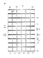
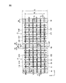
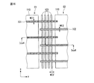
図1は、本発明の一実施の形態に係る太陽電池モジュールの全体様子を示す図であり、図2は、本発明の第1の実施の形態に係る太陽電池モジュールの後面平面様子を示す図であり、図3は、図2に適用される太陽電池の一例を示す図であり、図4は、図3に示された太陽電池の第1、第2電極(C141、C142)のパターンを示して図であり、図5は、図2でCSx1−CSx1ラインに沿った断面様子を示す図であり、図6は、コネクタの詳細の説明のために図2においてCSy1−CSy1ラインに沿った断面様子を示す図であり、図7は、コネクタ(Cn)の光反射効果を説明するための図である。 FIG. 1 is a diagram showing an overall state of a solar cell module according to an embodiment of the present invention, and FIG. 2 is a diagram showing a rear surface plan view of the solar cell module according to the first embodiment of the present invention. 3 is a diagram showing an example of the solar cell applied to FIG. 2, and FIG. 4 shows the pattern of the first and second electrodes (C141, C142) of the solar cell shown in FIG. FIG. 5 is a diagram showing a cross-sectional view along the CSx1-CSx1 line in FIG. 2, and FIG. 6 is a diagram along the CSy1-CSy1 line in FIG. 2 for explaining the connector in detail. FIG. 7 is a diagram showing a cross-sectional state, and FIG. 7 is a diagram for explaining the light reflection effect of the connector (Cn).
示されたように、この実施の形態の太陽電池モジュール10は、コネクタ(Cn)によって接続された複数の太陽電池モジュールが列をなして形成された複数のストリング11と互いに隣り合ったストリング11を接続させるブッシュ バー13を含みから構成されている。
As shown, the
まず、ストリング11は、複数の太陽電池110が1列で配置され、隣接したものとはコネクタ(Cn)によって互に接続され、1列のストリングが互いに接続されている。この図では、10個の太陽電池110が1列を成していることで例示し、第1乃至第6ストリング(11a−11f)が存在することで例示する。
First, in the
コネクタ(Cn)は、第1〜第6ストリング(11a−11f)内で太陽電池110と太陽電池110との間に配置されて隣接した二つの太陽電池を接続させる第1コネクタ(Cn1)と第1ストリング11aの一端と第6ストリング(11f)の一方の端だけそれぞれ接続されている第2コネクタ(Cn2)を含めて構成することがある。
The connector (Cn) is disposed between the
第1コネクタ(Cn1)と第2コネクタ(Cn2)は配置される位置でのみ異なり、基本的に後述するような同じ構成を有する。ただし、位置に違いがあるので、第2コネクタ(Cn2)は、第1配線(IC1)と第2配線(IC2)の内、いずれか1つでのみ接続がされるものの、第1コネクタ(Cn1)は、第1配線(IC1)と第2配線(IC2)のすべてが接続されるという点で違いがある。また、第1コネクタ(Cn1)と第2コネクタ(Cn2)は例外的に、表面に形成される凹凸の形状において違いがあることがある。これについては後述する。 The first connector (Cn1) and the second connector (Cn2) are different only at positions where they are arranged, and basically have the same configuration as described later. However, since there is a difference in position, the second connector (Cn2) is connected to only one of the first wiring (IC1) and the second wiring (IC2), but the first connector (Cn1) ) Is different in that all of the first wiring (IC1) and the second wiring (IC2) are connected. In addition, the first connector (Cn1) and the second connector (Cn2) are exceptionally different in the shape of the unevenness formed on the surface. This will be described later.
これにより、太陽電池11と、これに隣接した太陽電池11との間に位置して隣接している二つの太陽電池を接続させる第1コネクタ(Cn1)は1列に含まれている太陽電池110の数より1つ少なくする必要があるので、1列に対して9個の第1コネクタ(Cn1)が用いられ、第2コネクタ(Cn2)は、第1ストリング(11a)と第6ストリング(11f)の端に1つずつ、2個使用される。
As a result, the first connector (Cn1) for connecting the
このように、ストリング11は、コネクタ(Cn)で互に接続されている複数の太陽電池11が集まって構成され、太陽電池モジュール10は、このストリング11を少なくとも2つ以上含んで構成されるため、太陽電池モジュール10をなす複数の太陽電池110は、全体的にm*nマトリックス配列をなす。
As described above, the
そして、ブッシイング バー13は、ストリングの上下にそれぞれ位置し、互いに隣接している二つのストリングを接続させている。この実施の形態においては、太陽電池モジュール10は、6つのストリング11を含めて構成されるため、ストリングを直列接続するには、ブッッシング バー13は、5個が必要である。ブッシング バー13は、配置される位置に応じて、上部ブッシング バー13aと下部ブッシング バー13bに分けることがある。
The
上部ブッシング バー13aは、図に基づいてストリング11より上方に配置されており、下部ブッシング バー13bは、ストリング11より下側に配置されている。
The
図1において例示したように、第1列のストリング11aと第2列ストリング11b、第3列ストリング11cと第4列ストリング11d、そして第5列ストリング11eと第6列ストリング11fは、それぞれ下部ブッシング バー(13b)により互に接続されており、また、第2列ストリング11bと第3列ストリング11c、第4列ストリング11dと第5列ストリング11eは、上部ブッシング バー13aとも接続されている。
As illustrated in FIG. 1, the
このようにブッシング バー13aは、ストリングとストリングの間を接続しているので、コネクタ(Cn)よりは高い負荷(load)がかかる。それで、ブッシング バー13aは、コネクタ(Cn)よりは高い導電性を有する物質で形成されるか、断面積の大きさが、コネクタの断面積よりも大きく構成されることが望ましい。一例として、ブッシング バー13の幅は、コネクタ(Cn)の幅より広くしたり、ブッシング バー13の厚さがコネクタ(Cn)の厚さよりさらに厚いことがある。
Thus, since the
好ましい一形態として、コネクタ(Cn)とブッシング バー13は、同一の構成を有するように作成されることがあるが、例としてブッシング バー13は、図6を介して例示するコネクタ(Cn)と同様の構成を有するように形成されることが可能である。
As a preferred embodiment, the connector (Cn) and the
また、ブッシング バー13は、コネクタ(Cn)をなす金属物質を少なくとも1つ以上の同じように構成されることも可能である。例として、コネクタ(Cn)が鉛(Pb)またはスズ(Sn)の内、いずれか1つを含めて構成される場合、ブッシング バー13もコネクタ(Cn)と同様に、鉛(Pb)またはスズ(Sn)の内、いずれか1つを含めて構成されることがある。
In addition, the
また、ブッシング バー13とコネクタ(Cn)は、第1及び第2配線(IC1、IC2)と物理的に強固に付着しなければならないので、断面が長方形であるリボンで構成されることが望ましいが、第1及び第2配線(IC1、IC2)は熱変形を減少させ太陽電池が曲がる問題が発生しないようにブッシング バー13またはコネクタ(Cn)と異なるように、断面が円形であるワイヤ形状を有することが望ましい。
Further, since the
また、コネクタ(Cn)に接続される第1配線(IC1)と第2配線(IC2)、そしてブッシング バー13に接続される第1配線(IC1)と第2配線(IC2)は、すべてコネクタ(Cn)とブッシング バー13の後面に接続されて、モジュールの前面から見たとき、第1配線(IC1)と第2配線(IC2)がコネクタ(Cn)とブッシング バー13に接続された様子が見えないようにすること望ましい。
The first wiring (IC1) and the second wiring (IC2) connected to the connector (Cn), and the first wiring (IC1) and the second wiring (IC2) connected to the
一方、前述した説明においては、第2コネクタ(Cn2)が第1コネクタ(Cn1)と同じ構成で形成されることを説明したが、これとは異なり、ブッシング バー13を第2コネクタ(Cn2)で構成することやはり可能である。
On the other hand, in the above description, it has been described that the second connector (Cn2) is formed in the same configuration as the first connector (Cn1), but unlike this, the
以上は、太陽電池モジュールの全体様子を説明し、以下では、第1配線(IC1)と第2配線(IC2)、そしてコネクタ(Cn)により隣接した二つの太陽電池がどのように接続されているかを説明する。 The above describes the overall state of the solar cell module, and how the two adjacent solar cells are connected by the first wiring (IC1), the second wiring (IC2), and the connector (Cn) below. Will be explained.
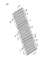
図2に示すように、この実施の形態において、太陽電池モジュールは、複数の太陽電池(C1、C2)、複数の太陽電池(C1、C2)の後面に形成された複数の第1、第2電極(C141、C142)に接続される複数の第1配線(IC1)と、複数の第2配線(IC2)、及び複数の第1、第2配線(IC1、IC2)に接続され、複数の太陽電池(C1、C2)を直列接続するコネクタ(Cn)を含む。 As shown in FIG. 2, in this embodiment, the solar cell module includes a plurality of first and second solar cells (C1, C2) and a plurality of first and second solar cells (C1, C2) formed on the rear surface. A plurality of first wirings (IC1) connected to the electrodes (C141, C142), a plurality of second wirings (IC2), and a plurality of first and second wirings (IC1, IC2), A connector (Cn) for connecting the batteries (C1, C2) in series is included.
ここで、複数の太陽電池(C1、C2)のそれぞれは、少なくとも半導体基板110と半導体基板110の後面に互いに離隔して形成される複数の第1電極(C141)と、複数の第2電極(C142)を備える。
Here, each of the plurality of solar cells (C1, C2) includes at least a plurality of first electrodes (C141) formed on the rear surface of the
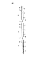
さらに具体的に説明すると、図3及び図4に示すように、本発明に係る太陽電池は、一例として、半導体基板110、反射防止膜130、エミッタ部121、後面電界部(back surface field: BSF、172)、複数の第1電極(C141)と、複数の第2電極(C142)を含むことがある。
More specifically, as shown in FIGS. 3 and 4, the solar cell according to the present invention includes, as an example, a
ここで、反射防止膜130と後面電界部172は省略されることもあるが、以下では、図3及び図4に示すように反射防止膜130と後面電界部172が含まれていることを一例として説明する。
Here, the
半導体基板110は、第1導電型、例えば、n型導電型のシリコンからなる半導体基板110で有り得る。このような半導体基板110は、結晶シリコンの材質で形成される半導体ウェハに第1導電型の不純物、例えばn型導電型の不純物がドーピングされて形成することがある。
The
エミッタ部121は、前面と対向している半導体基板110の後面内に複数個が互いに離隔して位置し、互いに並行する第1方向(x)に伸びている。このような複数のエミッタ部121は、半導体基板110の導電型と反対の第2導電型、例えばp型導電型の不純物が含まれることがある。
A plurality of
これにより、半導体基板110とエミッタ部121によってp−n接合が形成されることがある。
As a result, a pn junction may be formed by the
後面電界部172は、半導体基板110の後面内部に複数個が互いに離隔してい位置し、複数のエミッタ部121と並行する第1方向(x)に伸びている。したがって 図2及び図3に示したように、半導体基板110の後面において複数のエミッタ部121と、複数の後面電界部172は、交互に位置することがある。
A plurality of the rear surface
複数の後面電界部172は、半導体基板110と同じ第1導電型の不純物が半導体基板110より高濃度で含有したn++不純物部で有り得る。
The plurality of rear surface
複数の第1電極(C141)は、エミッタ部121とそれぞれ、物理的及び電気的に接続されてエミッタ部121に沿って半導体基板110の後面に形成することがある。
The plurality of first electrodes C <b> 141 may be formed on the rear surface of the
また、複数の第2電極(C142)は、複数の後面電界部172に沿って半導体基板110の後面に形成され、後面電界部172を介して半導体基板110とそれぞれ、物理的及び電気的に接続することがある。
The plurality of second electrodes (C142) are formed on the rear surface of the
ここで、複数の第1電極(C141)のそれぞれは、図3に示すように、第1方向(x)に伸びていることができ、複数の第1電極(C141)のそれぞれは、第1方向( x)と交差する第2方向(y)に互いに離隔して配列することがある。 Here, as shown in FIG. 3, each of the plurality of first electrodes (C141) can extend in the first direction (x), and each of the plurality of first electrodes (C141) In some cases, they are arranged apart from each other in the second direction (y) intersecting the direction (x).
さらに、複数の第2電極(C142)のそれぞれも、図3に示すように、第1方向(x)に伸びていることができ、複数の第2電極(C142)のそれぞれは、第1方向(x)と交差する第2方向(y)に互いに離隔して配列することがある。 Furthermore, each of the plurality of second electrodes (C142) can also extend in the first direction (x) as shown in FIG. 3, and each of the plurality of second electrodes (C142) can extend in the first direction. In some cases, they are arranged apart from each other in the second direction (y) intersecting (x).
また、複数の第1、第2電極(C141、C142)は、互いに離隔して、電気的に 隔離することができ、第1電極(C141)と第2電極(C142)が互いに交互して配置することがある。 The plurality of first and second electrodes (C141, C142) can be separated from each other and electrically isolated, and the first electrode (C141) and the second electrode (C142) are alternately arranged. There are things to do.
このように構成される複数の第1、第2電極(C141、C142)は、好ましい一形態で、コネクタ(Cn)やブッシングバー13を構成する金属物質と、少なくとも1つ以上の同一の物質で構成されることがある。コネクタ(Cn)やブッシングバー13は、複数の第1、第2電極(C141、C142)に溶融結合させるはんだ付け(soldering)方法で結合される。したがって、複数の第1、第2電極(C141、C142)がコネクタ(Cn)やブッシング バー13と同じ金属物質を含むようになれば、結合強度を高めることができるだけでなく、複数の第1、第2電極(C141、C142)、コネクタ(Cn)、ブッシング バー13を同時に結合させることが可能となる。
The plurality of first and second electrodes (C141, C142) configured in this way is a preferable embodiment, and is composed of at least one and the same material as the metal material constituting the connector (Cn) and the
このような構造で製造された本発明に係る太陽電池において、第1電極(C141)を介して収集された正孔と第2電極(C142)を介して収集された電子は、外部の回路装置を介して外部装置の電源で用いることがある。 In the solar cell according to the present invention manufactured with such a structure, the holes collected through the first electrode (C141) and the electrons collected through the second electrode (C142) are external circuit devices. It may be used as a power source of an external device via
本発明に係る太陽電池モジュールに適用された太陽電池は、必ず図3及び図4にのみ限定しなく、太陽電池に備えられる第1、第2電極(C141、C142)が半導体基板110の後面のみ形成される点を除外し、他の構成要素はいくらでも変更が可能である。
The solar cell applied to the solar cell module according to the present invention is not necessarily limited to FIGS. 3 and 4, and the first and second electrodes (C 141, C 142) provided in the solar cell are only on the rear surface of the
例えば、本発明の太陽電池モジュールにおいては、第1電極(C141)の一部とエミッタ部121が、半導体基板110の前面に位置し、第1電極(C141)の一部が半導体基板110に形成されたホールを介して半導体基板110の後面に形成された第1電極(C141)の残りの一部と接続されるMWTタイプの太陽電池も適用が可能である。
For example, in the solar cell module of the present invention, a part of the first electrode (C141) and the
このように、図3及び図4で説明した太陽電池は、図2に示すように、複数個が第2方向(y)に配列することがある。つまり、一例として、第1太陽電池(C1)と第2太陽電池(C2)は、第2方向(y)に配列することがある。 As described above, a plurality of solar cells described in FIGS. 3 and 4 may be arranged in the second direction (y) as shown in FIG. That is, as an example, the first solar cell (C1) and the second solar cell (C2) may be arranged in the second direction (y).
このとき、第1、第2太陽電池(C1、C2)に備えられる複数の第1、第2電極(C141、C142)の長さ方向が第1方向(x)に向くように配置することがある。 At this time, the first and second solar cells (C1, C2) may be arranged such that the length directions of the plurality of first and second electrodes (C141, C142) are directed to the first direction (x). is there.
このように、第1、第2太陽電池(C1、C2)が第2方向(y)に配列された状態で、第1、第2太陽電池(C1、C2)は、第1、第2配線(IC1、IC2)とコネクタ(Cn)によって互に接続されて太陽電池モジュールを構成し、この太陽電池モジュールが第2方向(y)に複数個配置された状態で、コネクタ(Cn)によって互に接続されて1つのストリングを形成することになる。 In this way, the first and second solar cells (C1, C2) are arranged in the second direction (y), and the first and second solar cells (C1, C2) are connected to the first and second wirings. (IC1, IC2) and the connector (Cn) are connected to each other to form a solar cell module, and a plurality of the solar cell modules are arranged in the second direction (y), and are connected to each other by the connector (Cn). Connected to form one string.
ここで、第1、第2配線(IC1、IC2)とコネクタ(Cn)は、導電性金属材質を含み、第1、第2配線(IC1、IC2)は、各太陽電池の半導体基板110の後面に接続され、太陽電池の直列接続のために、各半導体基板110に接続された第1、第2配線(IC1、IC2)は、コネクタ(Cn)に接続することがある。
Here, the first and second wirings (IC1, IC2) and the connector (Cn) include a conductive metal material, and the first and second wirings (IC1, IC2) are the rear surfaces of the
併せて、複数の第1、第2配線(IC1、IC2)は、幅と厚さが互いに同一の導電性ワイヤの形態であるか、幅が厚さより大きいリボンの形を有することがある。 In addition, the plurality of first and second wirings (IC1, IC2) may be in the form of conductive wires having the same width and thickness, or may have a ribbon shape having a width greater than the thickness.
具体的に、複数の第1配線(IC1)は、複数の太陽電池(C1、C2)の内直接隣接する二つの太陽電池の内、いずれか1つの太陽電池に備えられた複数の第1電極(C141)には、導電性接着剤(CA)を介して接続され、複数の第2電極(C142)については、絶縁層(IL)を介して絶縁され、複数の第2配線(IC2)は、もう一つの太陽電池に備えられた複数の第2電極(C142)には、導電性接着剤(CA)を介して接続され、複数の第1電極(C1412)については、絶縁層(IL)を介して絶縁することがある。 Specifically, the plurality of first wirings (IC1) are a plurality of first electrodes provided in any one of the two solar cells directly adjacent to each other among the plurality of solar cells (C1, C2). (C141) is connected via a conductive adhesive (CA), the plurality of second electrodes (C142) are insulated via an insulating layer (IL), and the plurality of second wirings (IC2) are In addition, a plurality of second electrodes (C142) provided in another solar cell are connected via a conductive adhesive (CA), and the plurality of first electrodes (C1412) are connected to an insulating layer (IL). It may be insulated through.
一例として、図2及び図6に示すように、複数の第1配線(IC1)は、互いに直接隣接する二つの第1、第2太陽電池(C1、C2)の内、第1太陽電池(C1)に備えられた複数の第1電極(C141)のみ接続することがある。 As an example, as shown in FIG. 2 and FIG. 6, the plurality of first wirings (IC1) is a first solar cell (C1) among two first and second solar cells (C1, C2) directly adjacent to each other. In some cases, only the plurality of first electrodes (C141) provided in the above are connected.
このとき、複数の第1配線(IC1)のそれぞれは、複数の第1電極(C141)の長さ方向と交差する第2方向(y)に長く配置することができ、図2に示すように、半導体基板110の後面から見たとき、複数個の第1配線(IC1)は、半導体基板110の外に引出されて形成することがある。
At this time, each of the plurality of first wirings (IC1) can be arranged long in the second direction (y) intersecting the length direction of the plurality of first electrodes (C141), as shown in FIG. When viewed from the rear surface of the
ここで、図2及び図5に示されたように、複数の第1配線(IC1)のそれぞれは、複数の第1電極(C141)に導電性接着剤(CA)を介して接続することがある。 Here, as shown in FIGS. 2 and 5, each of the plurality of first wirings (IC1) can be connected to the plurality of first electrodes (C141) via a conductive adhesive (CA). is there.
ここで、導電性接着剤(CA)は、金属材料間の接着力に優れたはんだペースト(半田paste)、絶縁性樹脂内に金属粒子が含有された導電性接着ペーストまたは導電性接着フィルムの内、いずれかが1つが用いられることがある。 Here, the conductive adhesive (CA) is a solder paste (solder paste) having an excellent adhesion between metal materials, a conductive adhesive paste containing conductive metal paste or a conductive adhesive film containing metal particles in an insulating resin. , Any one may be used.
さらに、複数の第1配線(IC1)のそれぞれと複数の第2電極(C142)との間との絶縁のために、複数の第1配線(IC1)と、複数の第2電極(C142)のそれぞれの間には、絶縁層(IL)が配置されることがある。 Furthermore, in order to insulate between each of the plurality of first wirings (IC1) and the plurality of second electrodes (C142), the plurality of first wirings (IC1) and the plurality of second electrodes (C142). An insulating layer (IL) may be disposed between each.
ここで、絶縁層(IL)は、絶縁性材質であればどのようなものでも構わないし、一例として、エポキシ(epoxy)のような絶縁性樹脂を用いることがある。 Here, the insulating layer (IL) may be any insulating material, and an insulating resin such as epoxy may be used as an example.
このとき、例えば、絶縁層(IL)に適用される材質は、溶解温度が約400℃以上であり、硬化温度が210℃〜250℃の間であることが望ましい。 At this time, for example, the material applied to the insulating layer (IL) preferably has a melting temperature of about 400 ° C. or higher and a curing temperature of 210 ° C. to 250 ° C.
一方、絶縁層(IL)の塗布面積は、導電性接着剤(CA)の塗布面積より大きい。つまり、図に示されたところのように、導電性接着剤(CA)の塗布面積は、絶縁層(IL)の塗布面積より小さい。導電性接着剤(CA)は、複数の第1配線(IC1)と第2配線(IC2)をそれぞれ複数の第1電極(C141)と第2電極(C142)と電気的に接続する構成であるが、絶縁層(IL)は、導電性接着剤(CA)と反対に、複数の第1配線(IC1)と第2配線(IC2)をそれぞれ複数の第1電極(C141)と第2電極(C142)と絶縁させる構成である。したがって、導電性接着剤(CA)の塗布面積が大きくなると、絶縁しなければならないところで導電性接着剤により電気的に接続されることがある。ため、この実施の形態では、このような点を考慮して 導電性接着剤(CA)の塗布面積は減少させ、絶縁層(IL)の塗布面積は広げ上記のような問題点が起こらないようにする。 On the other hand, the application area of the insulating layer (IL) is larger than the application area of the conductive adhesive (CA). That is, as shown in the figure, the application area of the conductive adhesive (CA) is smaller than the application area of the insulating layer (IL). The conductive adhesive (CA) is configured to electrically connect the plurality of first wirings (IC1) and the second wiring (IC2) to the plurality of first electrodes (C141) and the second electrodes (C142), respectively. However, the insulating layer (IL) has a plurality of first wirings (IC1) and second wirings (IC2), which are opposite to the conductive adhesive (CA), and a plurality of first electrodes (C141) and second electrodes ( C142). Therefore, when the application area of the conductive adhesive (CA) is increased, the conductive adhesive may be electrically connected where it must be insulated. Therefore, in this embodiment, the application area of the conductive adhesive (CA) is reduced in consideration of such points, and the application area of the insulating layer (IL) is widened so that the above problems do not occur. To.
次に、複数の第2配線(IC2)は、複数の太陽電池(C1、C2)の内、互いに直接隣接する二つの太陽電池の内、残りの一つの太陽電池に備えられた複数の第2電極(C142)に重畳されて、接続することがある。 Next, the plurality of second wirings (IC2) are a plurality of second wirings provided in the remaining one of the plurality of solar cells (C1, C2) that are directly adjacent to each other. There are cases where the electrodes (C142) are overlapped and connected.
一例として、図2及び図5に示すように、複数の第2配線(IC2)は、互いに直接隣接する二つの第1、第2太陽電池(C1、C2)の内、第2太陽電池(C2)に備えられた複数の第2電極(C142)に重畳され接続することがある。 As an example, as shown in FIG. 2 and FIG. 5, the plurality of second wirings (IC2) includes a second solar cell (C2) among two first and second solar cells (C1, C2) directly adjacent to each other. ) May be superimposed on and connected to the plurality of second electrodes (C142).
このとき、複数の第2配線(IC2)のそれぞれは、複数の第2電極(C142)の長さ方向と交差する第2方向(y)に長く配置することができ、図2に示すように、半導体基板110の後面から見たとき、複数個の第2配線(IC2)は、半導体基板110の外に引出されて形成することがある。
At this time, each of the plurality of second wirings (IC2) can be arranged long in the second direction (y) intersecting the length direction of the plurality of second electrodes (C142), as shown in FIG. When viewed from the rear surface of the
ここで、図2及び図5に示されたように、複数の第2配線(IC2)のそれぞれは、複数の第2電極(C142)に、前述したところと同じ導電性接着剤(CA)を介して接続することがある。 Here, as shown in FIG. 2 and FIG. 5, each of the plurality of second wirings (IC2) is provided with the same conductive adhesive (CA) as described above to the plurality of second electrodes (C142). May be connected through.
併せて、複数の第2配線(IC2)のそれぞれと複数の第1電極(C141)との間との絶縁のために、複数の第2配線(IC2)と、複数の第1電極(C141)のそれぞれの間には、前述したところと同じ絶縁層(IL)が配置されることがある。 In addition, a plurality of second wirings (IC2) and a plurality of first electrodes (C141) are provided for insulation between each of the plurality of second wirings (IC2) and the plurality of first electrodes (C141). In some cases, the same insulating layer (IL) as described above may be disposed between the two.
さらに、前では、第1配線(IC1)が第1太陽電池(C1)の第1電極(C141)に接続され、第2配線(IC2)が第2太陽電池(C2)の第2電極(C142)に接続されるものだけを説明したが、図2及び図5に示すように、第1太陽電池(C1)に備えられた複数の第2電極(C142)にも複数の第2配線(IC2)が導電性接着剤(CA)を介して接続することができ、第2太陽電池(C2)に備えられた複数の第1電極(C141)にも複数の第1配線(IC1)が導電性接着剤(CA)を介して接続することがある。 Furthermore, before, the first wiring (IC1) is connected to the first electrode (C141) of the first solar cell (C1), and the second wiring (IC2) is the second electrode (C142) of the second solar cell (C2). However, as shown in FIGS. 2 and 5, the plurality of second electrodes (C142) provided in the first solar cell (C1) also includes a plurality of second wirings (IC2). ) Can be connected through the conductive adhesive (CA), and the plurality of first wirings (IC1) are also conductive in the plurality of first electrodes (C141) provided in the second solar cell (C2). It may be connected via an adhesive (CA).
つまり、1つの太陽電池素子に形成される半導体基板110の後面には、複数個の第1配線(IC1)と複数の第2配線(IC2)が各セルの電極(C141、C142)に接続されることがある。
That is, a plurality of first wirings (IC1) and a plurality of second wirings (IC2) are connected to the electrodes (C141, C142) of each cell on the rear surface of the
したがって、図2及び図5に示すように、各太陽電池の第1電極(C141)には、第1配線(IC1)が接続され、第2電極(C142)には、第2配線(IC2)が接続することがある。 Therefore, as shown in FIGS. 2 and 5, the first wiring (IC1) is connected to the first electrode (C141) of each solar cell, and the second wiring (IC2) is connected to the second electrode (C142). May connect.
このように、各太陽電池の後面に接続された複数の第1配線(IC1)及び複数の第2配線(IC2)の内、各半導体基板110の外に引出される部分が図2及び図5に示されたように、第1、第2太陽電池(C1、C2)との間に配置されるコネクタ(Cn)の後面に接続することができ、これにより、複数の太陽電池(C1、C2)が一つのストリングに形成することがある。
As described above, portions of the plurality of first wirings (IC1) and the plurality of second wirings (IC2) connected to the rear surface of each solar cell are drawn out of each
このとき、コネクタ(Cn)の長さ方向は、各太陽電池の第1、第2電極(C141、C142)の長さ方向と同じ第1方向(x)に長く形成することがある。 At this time, the length direction of the connector (Cn) may be formed long in the same first direction (x) as the length direction of the first and second electrodes (C141, C142) of each solar cell.
ここで、コネクタ(Cn)は、一つまたは複数個であることがあるが、第1の実施の形態においては、コネクタ(Cn)が第1方向(x)に長く伸びた一つの金属パッドで形成された場合を一例として説明する。 Here, there may be one or a plurality of connectors (Cn), but in the first embodiment, the connector (Cn) is a single metal pad extending long in the first direction (x). The case where it is formed will be described as an example.
このとき、コネクタ(Cn)は、図2及び図5に示すように、各太陽電池に備えられた半導体基板110の間に配置することがある。つまり、コネクタ(Cn)は、複数の太陽電池(C1、C2)のそれぞれに備えられた半導体基板110と重畳されなく、離隔することができ、例えば、ストリングを後面から見たときに、図2に示すように、コネクタ(Cn)と第1太陽電池(C1)の半導体基板110との間はD1だけ離隔することができ、コネクタ(Cn)と第2太陽電池(C2)の半導体基板110との間は、D2だけ離隔することがある。このとき、D1とD2の離隔間隔は、互いに同一または異なることがある。
At this time, the connector (Cn) may be disposed between the
具体的には、D1とD2は、それぞれ、第1太陽電池(C1)と第2太陽電池(C2)との間の距離でコネクタの幅(WI3)を引いた値で決定されるが。一例として、50μm〜3mmの間で形成されることがある。一例として、D1とD2は、互いに同一に100μmで有り得、D1とD2の内、いずれか1つは、500μm、他の一つは、200μmになることもある。 Specifically, D1 and D2 are respectively determined by values obtained by subtracting the connector width (WI3) by the distance between the first solar cell (C1) and the second solar cell (C2). As an example, it may be formed between 50 μm and 3 mm. As an example, D1 and D2 may be the same 100 μm, and one of D1 and D2 may be 500 μm and the other may be 200 μm.
D1とD2の離隔間隔をこのように設定することは、各太陽電池(C1、C2)の半導体基板110とコネクタ(Cn)は、互に接続されて短絡することを防止し、各太陽電池(C1、C2)の半導体基板110とコネクタ(Cn)との間の空間に形成されたD1とD2に入射される光の量を最小化し、太陽電池モジュールの発電効率を最大化するためである。
Setting the separation distance of D1 and D2 in this way prevents the
このように、コネクタ(Cn)が半導体基板110の間に配置されることにより、各太陽電池間に入射された光を反射して太陽電池に再入射できるようにすることができ、併せて、各半導体基板110との間でコネクタ(Cn)が第1、第2配線(IC1、IC2)を固定させる役割をすることにより、太陽電池モジュールの構造的な安定性をさらに向上させることがある。
Thus, by arranging the connector (Cn) between the
コネクタ(Cn)の幅(WI3)は、十分な接着力と隣接したセル間の間隔を考慮してD1とD2の内、少なくとも一つと同じか大きく、好ましくは0.1mm〜20mmの範囲の値を有する。そして、コネクタの厚さは0.015mm〜2mmの間の値を有する。 The width (WI3) of the connector (Cn) is equal to or larger than at least one of D1 and D2 in consideration of sufficient adhesive force and the distance between adjacent cells, and preferably a value in the range of 0.1 mm to 20 mm. Have And the thickness of a connector has a value between 0.015 mm-2 mm.
コネクタ(Cn)の幅が小さすぎると、十分な接着力を得ることができないだけでなく、コネクタ(Cn)から反射される光の量が小さすぎる発電効率を上げることないので、コネクタの幅はD1とD2の内、少なくとも一つと同じか大きくなければならない。そして、コネクタ(Cn)の長さ(CL)は、コネクタ(Cn)に接続されている複数の第1配線と第2配線(IC1、IC2)の最初と最後に位置する二つの配線間の長さ(WL)と同じか大きいしなければならなく、太陽電池(C1、C2)の幅にストリングの間の幅(SL)を合わせたものよりは小さくなければならない。 If the width of the connector (Cn) is too small, not only a sufficient adhesive force cannot be obtained, but also the amount of light reflected from the connector (Cn) is too small to increase the power generation efficiency. Must be equal to or greater than at least one of D1 and D2. The length (CL) of the connector (Cn) is the length between two wirings positioned at the beginning and the end of the plurality of first wirings and second wirings (IC1, IC2) connected to the connector (Cn). Must be equal to or greater than (WL) and smaller than the width of the solar cells (C1, C2) plus the width (SL) between the strings.
もし、コネクタ(Cn)の長さ(CL)がWLより小さい場合コネクタ(Cn)に接続しなければならないすべての第1配線(IC1)と第2配線(IC2)が正常にコネクタ(Cn)に接続されないことがある。そして、コネクタ(Cn)の長さが太陽電池(C1、C2)の幅にストリングの間の幅(SL)を合わせたものと同じか大きくなると、コネクタ(Cn)が隣接したストリングと電気的に接続することがある。 If the length (CL) of the connector (Cn) is smaller than WL, all the first wiring (IC1) and the second wiring (IC2) that must be connected to the connector (Cn) are normally connected to the connector (Cn). May not be connected. When the length of the connector (Cn) is equal to or larger than the width of the solar cells (C1, C2) and the width (SL) between the strings, the connector (Cn) is electrically connected to the adjacent string. May connect.
そして、コネクタの厚さは、作業工程を考慮して、第1配線(IC1)または第2配線(IC2)の厚さと同じか小さいことが望ましい。金属物質で作られたコネクタ(Cn)の厚さが厚くなると、延性が小さくなって曲がったり曲げるのが容易でないため、第1配線(IC1)または第2配線(IC2)をコネクタに接合させることが容易ではないことがある。さらに、コネクタの延性が減ると、第1配線(IC1)または第2配線(IC2)が熱的変形を起こすとき、延性が小さくて接合部分でクラックが生じるなどの問題が発生することもある。 The thickness of the connector is preferably equal to or smaller than the thickness of the first wiring (IC1) or the second wiring (IC2) in consideration of the work process. When the thickness of the connector (Cn) made of a metal material is increased, the ductility is reduced and it is not easy to bend or bend. Therefore, the first wiring (IC1) or the second wiring (IC2) is joined to the connector. May not be easy. Further, when the ductility of the connector is reduced, when the first wiring (IC1) or the second wiring (IC2) is thermally deformed, there may be a problem that the ductility is small and a crack occurs at the joint portion.
さらに、図2では、各太陽電池において半導体基板110の後面に導電性接着剤(CA)を介して接続される第1、第2配線(IC1、IC2)の総数が6個である場合に図示したが、これは一例に過ぎず、各太陽電池において半導体基板110の後面に接続される第1、第2配線(IC1、IC2)の総数は、6個〜40個の間であり、さらに好ましくは太陽電池の大きさが156mm*156mmであれば、28〜32個の間で決定することがある。
Further, FIG. 2 shows the case where the total number of first and second wirings (IC1, IC2) connected to the rear surface of the
このとき、図2及び図5に示すように、第1太陽電池(C1)に接続された第1配線(IC1)と第2太陽電池(C2)に接続された第2配線(IC2)は互いに異なるライン上に位置してそれぞれ独立的、個別的に備えられることにより、コネクタ(Cn)と重畳される部分に位置する第1配線(IC1)の先端と第2配線(IC2)の先端は、DC1ほど互いに離隔されることがある。したがって、第1配線(IC1)の先端と第2配線(IC2)の先端は、ずれる(offset)ことがある。 At this time, as shown in FIGS. 2 and 5, the first wiring (IC1) connected to the first solar cell (C1) and the second wiring (IC2) connected to the second solar cell (C2) are mutually connected. By being provided independently and individually on different lines, the tip of the first wire (IC1) and the tip of the second wire (IC2) located at the portion overlapping the connector (Cn) are DC1 may be separated from each other. Therefore, the tip of the first wiring (IC1) and the tip of the second wiring (IC2) may be offset.
したがって、複数の太陽電池の内、第1、第2配線(IC1、IC2)と、第1、第2電極(C141、C142)の間に接続不良が発生した太陽電池がある場合、コネクタ(Cn)と、複数の第1、第2配線(IC1、IC2)との間の接続を解除して、その太陽電池だけ、さらに容易に交換することがある。 Therefore, when there is a solar cell in which connection failure occurs between the first and second wirings (IC1, IC2) and the first and second electrodes (C141, C142) among the plurality of solar cells, the connector (Cn ) And the plurality of first and second wirings (IC1, IC2) may be released, and only the solar cell may be replaced more easily.
さらに、コネクタ(Cn)が第1、第2配線(IC1、IC2)のいずれか1つと、重畳する領域(OA)は、コネクタ(Cn)の幅(WI3)と同じか小さく、コネクタ(Cn)の幅(WI3)×1/3と同じか大きい値を有することが好ましい。もし 重畳領域(OA)がコネクタ(Cn)の幅(WI3)より大きくなると、第1、第2配線(IC1、IC2)がコネクタ(Cn)の外に飛び出すようにされるので、デザイン面で見栄えが良くないだけでなく、接続されてはいけないことと接続される問題が発生する素地がある。そして、重なる領域(OA)がコネクタ(Cn)の幅(WI3×1/3より小さくなると接合面積が小さく、第1、第2配線(IC1、IC2)がコネクタ(Cn)に安定的に結合されない問題がある。 Further, the area (OA) where the connector (Cn) overlaps one of the first and second wirings (IC1, IC2) is equal to or smaller than the width (WI3) of the connector (Cn), and the connector (Cn) It is preferable to have a value equal to or larger than the width (WI3) × 1/3. If the overlap area (OA) is larger than the width (WI3) of the connector (Cn), the first and second wirings (IC1, IC2) will jump out of the connector (Cn). In addition to being bad, there are grounds where connection problems occur that must not be connected. When the overlapping area (OA) is smaller than the width (WI3 × 1/3) of the connector (Cn), the bonding area is small, and the first and second wirings (IC1, IC2) are not stably coupled to the connector (Cn). There's a problem.
さらに、第1配線(IC1)と第2配線(IC2)は、コネクタ(Cn)に配置されることが好ましく、向き合っているペーシング距離(FA)は、コネクタの幅と同じか、小さい。電極で収集された電荷はコネクタで、第1配線から第2配線に、または第2配線から第1配線に伝達される。したがって、第1配線(IC1)と第2配線(IC2)は、コネクタ(Cn)に向い合っていると効率的に電荷を伝達することがある。 Further, the first wiring (IC1) and the second wiring (IC2) are preferably arranged on the connector (Cn), and the pacing distance (FA) facing each other is the same as or smaller than the width of the connector. The charges collected by the electrodes are transmitted from the first wiring to the second wiring or from the second wiring to the first wiring at the connector. Therefore, when the first wiring (IC1) and the second wiring (IC2) face the connector (Cn), charges may be efficiently transmitted.
しかし、これとは異なり、コネクタ(Cn)と重なる部分で第1配線(IC1)と第2配線(IC2)は、互いに離隔しなく一体に接続されることも可能である。これについては、本発明の第2の実施の形態でさらに具体的に説明する。 However, unlike this, the first wiring (IC1) and the second wiring (IC2) can be integrally connected without being separated from each other at the portion overlapping the connector (Cn). This will be described more specifically in the second embodiment of the present invention.
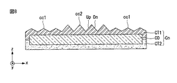
ここで、コネクタ(Cn)のさらに具体的な構造について、図6を参照して説明すると、次の通りである。 Here, a more specific structure of the connector (Cn) will be described with reference to FIG.
図6に示すように、コネクタ(Cn)は、導電性の第1金属材で形成されるコア(CO)、コア(CO)の入射面側の表面にコーティングされて位置する第1コーティング部(CT1)、及びコア(CO)の後面側の表面にコーティングされて位置する第2コーティング部(CT2)を含む形成することがある。 As shown in FIG. 6, the connector (Cn) includes a core (CO) formed of a conductive first metal material, and a first coating portion (coating on the incident surface side surface of the core (CO)). CT1) and a second coating portion (CT2) that is located on the rear surface of the core (CO) may be formed.
ここで、コア(CO)の第1金属材は、伝導性が良好な金属材質、例えば、銅(Cu)、Al、Niのような物質が用いられることがある。 Here, the first metal material of the core (CO) may be a metal material having good conductivity, for example, a material such as copper (Cu), Al, or Ni.
ここで、第1コーティング部(CT1)の入射面側の表面には、図6に示すように、複数の凹凸が備えられることがある。このような凹凸は、コネクタ(Cn)に入射する光を散乱させるためにピラミッド状の構造に形成することがある。 Here, the surface on the incident surface side of the first coating portion (CT1) may be provided with a plurality of irregularities as shown in FIG. Such irregularities may be formed in a pyramidal structure in order to scatter light incident on the connector (Cn).
併せて、このような第1コーティング部(CT1)は、コネクタ(Cn)による反射率を高めるために、第1金属材より表面反射率が高い第2金属材を含むことがある。一例として、第2金属材は、第1金属材である銅(Cu)より表面反射率の高い銀(Ag)が用いられる。 In addition, the first coating part (CT1) may include a second metal material having a surface reflectance higher than that of the first metal material in order to increase the reflectance by the connector (Cn). As an example, the second metal material is silver (Ag) having a higher surface reflectance than copper (Cu), which is the first metal material.
また、第2コーティング部(CT2)は、コネクタ(Cn)材の後面に接続された複数の第1、第2配線(IC1、IC2)材との接触力と接触抵抗をさらに向上させるために、第1、 2金属材より融点の低い第3金属材を含むことがある。 Further, the second coating part (CT2) is for further improving the contact force and contact resistance with the plurality of first and second wiring (IC1, IC2) materials connected to the rear surface of the connector (Cn) material. A third metal material having a lower melting point than the first and second metal materials may be included.
一例として、第3金属材は、第1、第2金属材である銅(Cu)や銀(Ag)より融点が低くて接着力が良いスズ(Sn)やインジウム(In)の内、少なくとも一つの金属材質を含むことことがある。さらに具体的には、第3金属材は一例として、SnをベースにするSnPb、SnAgCu、SnZnBi、SnCu、SnAgのような合金(alloy)またはInなどのような物質を含むことがある。このように第2コーティング部(CT2)がはんだ物質を含めば、コネクタ(Cn)は、第1及び第2配線(IC1、IC2)と母材を熱加熱して溶融結合させるはんだ付け方法で物理的、電気的に接続されることがある。別の方法として、コネクタ(Cn)は、第1及び第2配線(IC1、IC2)とポリマーに導電性金属粒子が入っているConductive Filmや、前述した導電性接着剤を介して結合されることもまた可能である。 As an example, the third metal material is at least one of tin (Sn) and indium (In) having a lower melting point and better adhesion than the first and second metal materials copper (Cu) and silver (Ag). May contain two metallic materials. More specifically, the third metal material may include, for example, an Sn-based alloy such as SnPb, SnAgCu, SnZnBi, SnCu, SnAg, or a material such as In. Thus, if the second coating part (CT2) includes a solder substance, the connector (Cn) is physically bonded by a soldering method in which the first and second wirings (IC1, IC2) and the base material are heated and melt-bonded. May be electrically and electrically connected. As another method, the connector (Cn) is bonded to the first and second wirings (IC1, IC2) through a conductive film containing conductive metal particles in a polymer or the conductive adhesive described above. Is also possible.
さらに、第2コーティング部(CT2)の後面表面には、図5に示すように、複数の第1、第2配線(IC1、IC2)が挿入される複数個の溝(HIC)が備えられることがある。つまり、第2コーティング部(CT2)の後面の表面に形成された複数個の溝(HIC)のそれぞれは、複数の第1、第2配線(IC1、IC2)が噛み合うことがある構造を有することがある。 Further, as shown in FIG. 5, a plurality of grooves (HIC) into which a plurality of first and second wirings (IC1, IC2) are inserted are provided on the rear surface of the second coating part (CT2). There is. In other words, each of the plurality of grooves (HIC) formed on the rear surface of the second coating part (CT2) has a structure in which the plurality of first and second wirings (IC1, IC2) may be engaged with each other. There is.
これにより、第2コーティング部(CT2)と第1、2配線(IC1、IC2)間の 接続面積を増加させ接触抵抗を最小化することができ、複数の第1、第2配線(IC1、IC2)をコネクタ(Cn)に接続させる際に、第1、第2配線(IC1、IC2)をさらに容易にアライン及び固定することができる。 Accordingly, the connection area between the second coating part (CT2) and the first and second wirings (IC1, IC2) can be increased and the contact resistance can be minimized, and the plurality of first and second wirings (IC1, IC2) can be achieved. ) To the connector (Cn), the first and second wirings (IC1, IC2) can be more easily aligned and fixed.
このとき、第2コーティング部(CT2)において溝(HIC)が形成されない部分の厚さ(TCT2)は、第2コーティング部(CT2)の接続力が十分に発揮されるようにするために、5μm〜30μm間に形成することがある。 At this time, the thickness (TCT2) of the portion where the groove (HIC) is not formed in the second coating portion (CT2) is 5 μm so that the connection force of the second coating portion (CT2) is sufficiently exerted. It may be formed between ˜30 μm.
もし第2コーティング部(CT2)の厚さが十分でない場合には、前述した導電性接着剤(CA)を用いて、第1、第2配線(IC1、IC2)をコネクタ(Cn)に接続することがある。 If the thickness of the second coating portion (CT2) is not sufficient, the first and second wirings (IC1, IC2) are connected to the connector (Cn) using the conductive adhesive (CA) described above. Sometimes.
しかし、前述したように、第2コーティング部(CT2)の厚さが5μm〜30μmの間である場合、別の導電性接着剤(CA)が必要ないため、製造工程をさらに単純化することができ、製造コストをさらに減小させることができる。 However, as described above, when the thickness of the second coating part (CT2) is between 5 μm and 30 μm, a separate conductive adhesive (CA) is not required, which can further simplify the manufacturing process. The manufacturing cost can be further reduced.
このように、第1、第2配線(IC1、IC2)とコネクタ(Cn)により複数個の太陽電池(C1、C2)が直列接続されたストリングは、透明基板(FG)と第1充填材(EC1)と、第2充填材(EC2)及び後面シート(BS)との間に配置された状態で一緒にラミネート(lamination)され、図7に示すように、一つの一体化されたモジュールで形成することができる。 As described above, the string in which the plurality of solar cells (C1, C2) are connected in series by the first and second wirings (IC1, IC2) and the connector (Cn) includes the transparent substrate (FG) and the first filler ( EC1), laminated together between the second filler (EC2) and the back sheet (BS) and laminated together, as shown in FIG. 7, formed in one integrated module can do.
ここで、透明基板(FG)は、光透過性のガラスまたはプラスチック材質で有り得、第1、第2充填材(EC1、EC2)は弾性力と絶縁性を備えた材質であり、例えば、EVAを含むことがある。さらに、後面シート(BS)は、防湿機能を有する絶縁性材質で形成することができる。 Here, the transparent substrate (FG) may be made of a light-transmitting glass or plastic material, and the first and second fillers (EC1, EC2) are materials having elasticity and insulation, for example, EVA. May contain. Further, the rear sheet (BS) can be formed of an insulating material having a moisture-proof function.
このように、複数個の太陽電池との間に反射体の役割をするコネクタ(Cn)を用いる場合、図7に示すように、太陽電池の間に入射される光をコネクタ(Cn)と透明基板(FG)を介して再び太陽電池に入射させることができ、太陽電池の効率をさらに向上させることができる。 Thus, when using the connector (Cn) which acts as a reflector between a plurality of solar cells, as shown in FIG. 7, the light incident between the solar cells is transparent to the connector (Cn). The light can enter the solar cell again through the substrate (FG), and the efficiency of the solar cell can be further improved.
以上の説明では、コネクタ(Cn)が太陽電池モジュールの入射面にさらに近く位置するに第1配線(IC1)と第2配線(IC2)がのすべてコネクタ(Cn)の底面に固定されるもので説明したが、これとは異なり、第1配線(IC1)と第2配線(IC2)がすべてコネクタ(Cn)の上面に固定されたり、第1配線(IC1)と第2配線(IC2)が互いに異なる面に固定されることもある。 In the above description, the first wiring (IC1) and the second wiring (IC2) are all fixed to the bottom surface of the connector (Cn) when the connector (Cn) is located closer to the incident surface of the solar cell module. Unlike the above, the first wiring (IC1) and the second wiring (IC2) are all fixed to the upper surface of the connector (Cn), or the first wiring (IC1) and the second wiring (IC2) are mutually connected. It may be fixed to different surfaces.
一方、図5においては、コネクタ(Cn)に複数の凹凸が備えない場合を一例として示したが、コネクタ(Cn)は、隣接した二つの太陽電池に光を反射させるためにコネクタ(Cn)の入射面側には図6、図8〜図11に例示するところような複数の凹凸を備えることも可能である。 On the other hand, in FIG. 5, the case where the connector (Cn) is not provided with a plurality of projections and depressions is shown as an example, but the connector (Cn) is a connector (Cn) for reflecting light to two adjacent solar cells. A plurality of projections and depressions as illustrated in FIGS. 6 and 8 to 11 can be provided on the incident surface side.
まず、図6において例示するところのように、第1コーティング部(CT1)の表面は、大きさが等しい凹凸(CC)を含むことが可能である。凹凸(CC)は、示されたところのような上り傾斜面(Up)と下り傾斜面(Dn)を含みから構成されるため、凹凸(CC)に入射された光は、上り傾斜面(Up)は、コネクタ(Cn)を基準に左に反射され、下り傾斜面(Dn)では、右に反射される。結果的に、コネクタ(Cn)に入射された光は、凹凸(CC)のためにコネクタによって接続された隣接した二太陽電池のそれぞれに追加で供給されることがある。 First, as illustrated in FIG. 6, the surface of the first coating portion (CT1) can include unevenness (CC) having the same size. Since the unevenness (CC) is configured to include an upward inclined surface (Up) and a downward inclined surface (Dn) as shown, the light incident on the unevenness (CC) is the upward inclined surface (Up). ) Is reflected to the left with reference to the connector (Cn), and is reflected to the right on the descending slope (Dn). As a result, light incident on the connector (Cn) may be additionally supplied to each of the adjacent two solar cells connected by the connector because of the unevenness (CC).
または、図8、図9において例示するような第1コーティング部(CT1)の表面は、大きさが異なる第1凹凸(CC1)と第2凹凸(CC2)を含んで構成することも可能である。 Alternatively, the surface of the first coating portion (CT1) as exemplified in FIGS. 8 and 9 can be configured to include first unevenness (CC1) and second unevenness (CC2) having different sizes. .
図8及び図9に例示する凹凸(CC)もまた図6に例示するよう同様に上り傾斜面(Up)と下り傾斜面(Dn)を含めて構成されるという点では同じである。 The unevenness (CC) illustrated in FIG. 8 and FIG. 9 is also the same in that it includes the upward inclined surface (Up) and the downward inclined surface (Dn) as illustrated in FIG.
ただし、図8及び図9に例示する凹凸(CC)は、位置に応じて、凹凸の大きさが異なるという点で違いがある。図8で例示するところによると、凹凸(CC)は、第1凹凸(CC1)とこれより大きな大きさを有する第2凹凸(CC2)を含む。ここで、大きさは、凹凸の断面積を意味する。 However, the unevenness (CC) illustrated in FIGS. 8 and 9 is different in that the size of the unevenness varies depending on the position. As illustrated in FIG. 8, the unevenness (CC) includes a first unevenness (CC1) and a second unevenness (CC2) having a larger size. Here, the size means the cross-sectional area of the unevenness.
コネクタ(Cn)の長さ方向(図のy軸方向)と交差する方向(図のx軸方向)に基づいて、コネクタ(Cn)の中心には、第2凹凸(CC2)が形成されることがあり、その他の部分には、第1凹凸(CC1)が形成されることがある。また、選択的に図9で例示するところのような、コネクタ(Cn)の中心には、第1凹凸(CC1)が形成され、それ以外の部分には、第2凹凸(CC2)が形成されることもまた可能である。 Based on the direction (x-axis direction in the figure) intersecting the length direction (y-axis direction in the figure) of the connector (Cn), the second unevenness (CC2) is formed at the center of the connector (Cn). In other parts, the first unevenness (CC1) may be formed. In addition, as illustrated in FIG. 9, the first unevenness (CC1) is formed at the center of the connector (Cn), and the second unevenness (CC2) is formed at the other portions. It is also possible.
ここで、コネクタ(Cn)の中心は、コネクタ(Cn)の長さ方向(図のy軸方向)と交差する方向(図のx軸方向)にコネクタを3等分したとき、中心部であり、断面全体の幅の20%よりは大きく、40%よりは小さな値から選択することができる。 Here, the center of the connector (Cn) is the center when the connector is equally divided into three in the direction (x-axis direction in the figure) intersecting the length direction (y-axis direction in the figure) of the connector (Cn). The value can be selected from a value larger than 20% of the entire width of the cross section and smaller than 40%.
図8に示すように中心に大きさが大きい第2凹凸(CC2)が配置されると、中心では、第1凹凸(CC1)より高い高さで光を反射させることができ、中心から反射された光が第1凹凸(CC1)により反射が邪魔された問題を減らすことができる。 As shown in FIG. 8, when the second unevenness (CC2) having a large size is arranged at the center, light can be reflected at a height higher than the first unevenness (CC1) at the center and reflected from the center. The problem that the reflection of light is disturbed by the first unevenness (CC1) can be reduced.
一方、図10及び図11においては、凹凸(CC‘)が上り傾斜面や下り傾斜面だけで構成される例を示している。図10において例示する凹凸(CC’)は上り傾斜面(Up)のみを含みから構成される場合を示しており、図11において例示する凹凸(CC‘)は下り傾斜面(Dn)のみを含みから構成される場合を示す。 On the other hand, in FIG.10 and FIG.11, the unevenness | corrugation (CC ') has shown the example comprised only by an up inclination surface or a down inclination surface. 10 illustrates a case where the unevenness (CC ′) illustrated in FIG. 10 includes only an upward inclined surface (Up), and the unevenness (CC ′) illustrated in FIG. 11 includes only a downward inclined surface (Dn). The case where it consists of is shown.
このように凹凸(CC‘)が上り傾斜面や下り傾斜面のみを選択的に含みから構成される場合に、コネクタ(Cn)は、いずれかの1つの方向にのみ光を反射させることになる。したがって、図1を介して説明したように、太陽電池と太陽電池との間に位置する第1コネクタ(Cn1)よりはストリングの一端にのみ位置する第2コネクタ(Cn2)にさらに有効に用いられる。つまり、第2コネクタ(Cn2)はストリングの一端にのみ位置しているので、凹凸は上り傾斜面や下り傾斜面のみを含むように構成されることが好ましく、第1コネクタ(Cn1)は、上り傾斜面と下り傾斜面のすべてを有するように構成されることが望ましい。 In this way, when the unevenness (CC ′) is configured to selectively include only an upward inclined surface or a downward inclined surface, the connector (Cn) reflects light only in any one direction. . Therefore, as described with reference to FIG. 1, the second connector (Cn2) positioned only at one end of the string is more effectively used than the first connector (Cn1) positioned between the solar cells. . That is, since the second connector (Cn2) is located only at one end of the string, it is preferable that the unevenness includes only an upward inclined surface and a downward inclined surface, and the first connector (Cn1) It is desirable to be configured to have all of the inclined surface and the downward inclined surface.
以上の説明は、コネクタ(Cn)に凹凸が形成されることで説明したが、ブッシング バー13にも、前述したように、上り傾斜面(Up)と下り傾斜面(Dn)を有する凹凸や、上り傾斜面(Up)と下り傾斜面(Dn)の内、いずれか一つだけで形成された凹凸が形成されることやはり可能である。
In the above description, the connector (Cn) is formed with unevenness. However, as described above, the
一例として、図1を基準にすると、上部ブッシング バー13aは、光モジュールの内側に反射させることができるように下り傾斜面だけを有する凹凸が形成されることがあり、下部ブッシング バー13bは、上り傾斜面のみ有する凹凸が形成されることがある。
As an example, with reference to FIG. 1, the
また、コネクタの高さは隣接した二つの太陽電池の高さより高いことが好ましいが、このように構成すると、光が反射されるコネクタの上面が太陽電池より高い位置に位置しており、コネクタから反射された光が隣接した二つ太陽電池によく伝達されることができる。 In addition, the height of the connector is preferably higher than the height of two adjacent solar cells, but when configured in this way, the upper surface of the connector from which light is reflected is located at a higher position than the solar cell. The reflected light can be transmitted well to two adjacent solar cells.
以下、太陽電池モジュールの第2の実施の形態について説明する。 Hereinafter, a second embodiment of the solar cell module will be described.
これまでの第1の実施の形態においては、第1太陽電池(C1)に接続された第1配線(IC1)と第2太陽電池(C2)に接続された第2配線(IC2)は互いに異なるライン線上に位置してそれぞれ独立的、個別的に備えられることにより、コネクタ(Cn)と重なる部分に位置する第1配線(IC1)の先端と第2配線(IC2)の先端は、互いに離隔される場合に対してのみ説明したが、これと異なり、以下の第2の実施の形態においては、第1太陽電池(C1)に接続された第1配線(IC1)と第2太陽電池(C2)に接続された第2配線(IC2)が一体に形成される場合について説明する。 In the first embodiment thus far, the first wiring (IC1) connected to the first solar cell (C1) and the second wiring (IC2) connected to the second solar cell (C2) are different from each other. By being provided independently and individually on the line line, the tip of the first wiring (IC1) and the tip of the second wiring (IC2) located in the portion overlapping the connector (Cn) are separated from each other. However, in the following second embodiment, the first wiring (IC1) and the second solar cell (C2) connected to the first solar cell (C1) are different. A case will be described in which the second wiring (IC2) connected to is integrally formed.
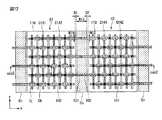
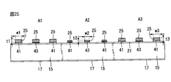
図12及び図13は、本発明に係る太陽電池モジュールの第2の実施の形態を説明するための図である。ここで、図12は、本発明の第2の実施の形態に係る太陽電池モジュールの後面の様子を示して、図13は、図12でCSx2−CSx2ラインに沿った断面図を示したものである。 FIG.12 and FIG.13 is a figure for demonstrating 2nd Embodiment of the solar cell module which concerns on this invention. Here, FIG. 12 shows a state of the rear surface of the solar cell module according to the second embodiment of the present invention, and FIG. 13 shows a cross-sectional view along the CSx2-CSx2 line in FIG. is there.
図12及び図13に示すように、第1太陽電池(C1)に接続された第1配線(IC1)と第2太陽電池(C2)に接続された第2配線(IC2)は、一体に形成することができ、これにより、3配線(IC3)と重なる部分で第1配線(IC1)と第2配線(IC2)は、互いに離隔しなく一体に形成することができる。したがって、第1配線(IC1)の先端と第2配線(IC2)の先端は、同一線上に位置することができる。 As shown in FIGS. 12 and 13, the first wiring (IC1) connected to the first solar cell (C1) and the second wiring (IC2) connected to the second solar cell (C2) are integrally formed. Accordingly, the first wiring (IC1) and the second wiring (IC2) can be integrally formed without being separated from each other in a portion overlapping with the three wirings (IC3). Therefore, the tip of the first wiring (IC1) and the tip of the second wiring (IC2) can be located on the same line.
したがって、第1太陽電池(C1)に接続された複数の第1配線(IC1)と第2太陽電池(C2)に接続された複数の第2配線(IC2)のそれぞれは、同一ライン線上に位置することができる。 Accordingly, the plurality of first wirings (IC1) connected to the first solar cell (C1) and the plurality of second wirings (IC2) connected to the second solar cell (C2) are positioned on the same line line. can do.
このとき、図12及び図13に示すように、第1太陽電池(C1)に接続された複数の第1配線(IC1)は、複数の第1電極(C141)に導電性接着剤(CA)を介して接続され、第2太陽電池(C2)に接続された複数の第2配線(IC2)は、複数の第2電極(C142)に導電性接着剤(CA)を介して接続することができる。 At this time, as shown in FIGS. 12 and 13, the plurality of first wirings (IC1) connected to the first solar cell (C1) are connected to the plurality of first electrodes (C141) by the conductive adhesive (CA). The plurality of second wirings (IC2) connected via the second solar cell (C2) may be connected to the plurality of second electrodes (C142) via the conductive adhesive (CA). it can.
これまでの第1、第2の実施の形態では、コネクタ(Cn)が各太陽電池の半導体基板110との間に位置し、各半導体基板110と重畳されず、離間して配置される場合だけを一例として説明したが、これと異なりコネクタ(Cn)が各太陽電池の半導体基板110との間に位置するが、一部の半導体基板110とは、重畳されて配置されることもある。これについて説明すると、次の通りである。
In the first and second embodiments thus far, only when the connector (Cn) is positioned between the
図14及び図15は、本発明に係る太陽電池モジュールの第3実施の形態を説明するための図である。ここで、図14は、本発明の第3の実施の形態に係る太陽電池モジュールの後面の様子を示した図であり、図15は、図14でCSx3−CSx3ラインに沿った断面図を示したものである。 FIG.14 and FIG.15 is a figure for demonstrating 3rd Embodiment of the solar cell module which concerns on this invention. Here, FIG. 14 is a view showing a state of the rear surface of the solar cell module according to the third embodiment of the present invention, and FIG. 15 is a cross-sectional view taken along the line CSx3-CSx3 in FIG. It is a thing.
この実施の形態においては、コネクタ(Cn)の少なくとも一部は、複数の太陽電池(C1、C2)に備えられた半導体基板110の内、一部の半導体基板110と重畳されて配置されることがある。
In this embodiment, at least a part of the connector (Cn) is arranged so as to overlap with a part of the
一例として、図14及び図15に示すように、コネクタ(Cn)の一部が、第1太陽電池(C1)の半導体基板110とは、重畳され、第2太陽電池(C2)の半導体基板110とは離隔された状態で配置されて形成されることも可能である。
As an example, as shown in FIGS. 14 and 15, a part of the connector (Cn) is overlapped with the
しかし、これと異なり、コネクタ(Cn)の全領域が第1太陽電池(C1)の半導体基板110と重畳されることも可能である。
However, unlike this, the entire region of the connector (Cn) can be overlapped with the
このとき、第1太陽電池(C1)に接続された第1配線(IC1)は、コネクタ(Cn)の前面に接続することができ、第2太陽電池(C2)に接続された第2配線(IC2)はコネクタ(Cn)の後面に接続することがある。 At this time, the first wiring (IC1) connected to the first solar cell (C1) can be connected to the front surface of the connector (Cn), and the second wiring (C2) connected to the second solar cell (C2) ( IC2) may be connected to the rear surface of the connector (Cn).
さらに、第1太陽電池(C1)の半導体基板110とコネクタ(Cn)が重畳される領域の中で第1配線(IC1)が位置しない領域には、コネクタ(Cn)と半導体基板110との不必要な短絡を防止するために、図10に示すように、絶縁層(IL)が形成されることがある。
Furthermore, in a region where the first wiring (IC1) is not located in a region where the
さらに、図14及び図15においては、第1太陽電池(C1)に接続された第1配線(IC1)が第1太陽電池(C1)の半導体基板110の外に引出されて形成された場合を一例として示したが、第1配線(IC1)が第1太陽電池(C1)の半導体基板110の外に引出されないこともある。
Further, in FIGS. 14 and 15, the first wiring (IC1) connected to the first solar cell (C1) is formed by being drawn out of the
これまで本発明の第1乃至第3実施の形態においては、コネクタ(Cn)が第1方向(x)に長く伸びた一つの金属パッドに形成された場合だけを例として説明したが、コネクタ(Cn)は、複数個で形成することもできる。これについて説明すると、次の通りである。 In the first to third embodiments of the present invention, the connector (Cn) has been described as an example only when it is formed on one metal pad extending in the first direction (x). A plurality of Cn) can be formed. This will be described as follows.
図16及び図17は、本発明に係る太陽電池モジュールの第4の実施の形態を説明するための図である。ここで、図16は、本発明の第4の実施の形態に係る太陽電池モジュールの後面の様子を示した図であり、図17は、図16でCSx4-CSx4ラインに沿った断面図を示のことである。 FIG.16 and FIG.17 is a figure for demonstrating 4th Embodiment of the solar cell module which concerns on this invention. Here, FIG. 16 is a view showing a state of the rear surface of the solar cell module according to the fourth embodiment of the present invention, and FIG. 17 is a sectional view taken along the line CSx4-CSx4 in FIG. That is.
図16及び図17に示すように、コネクタ(Cn)は、互いに離隔して、第1方向(x)に長く伸びた複数個で形成することができる。 As shown in FIGS. 16 and 17, the connectors (Cn) can be formed by a plurality of connectors that are spaced apart from each other and extend long in the first direction (x).
このような場合にも、第1方向(x)に長く伸びた複数個のコネクタ(Cn)を介して太陽電池の間に入射される光を太陽電池に再入射して、太陽電池モジュールの効率をさらに向上させることがある。 Also in such a case, the light incident between the solar cells through the plurality of connectors (Cn) extended in the first direction (x) is re-incident on the solar cells, and the efficiency of the solar cell module May be further improved.
このとき、複数個のコネクタ(Cn)も、また前述したように、コア(CO)、第1コーティング部(CT1)及び第2コーティング部(CT2)を含むことできる。 At this time, the plurality of connectors (Cn) may also include the core (CO), the first coating part (CT1), and the second coating part (CT2) as described above.
さらに、第4の実施の形態のような場合、コネクタ(Cn)の幅(WI3)は、第1、第2配線(IC1、IC2)の幅(WI1、WI2)と同じことがある。しかし、セル間の直列抵抗を確保するためにコネクタ(Cn)の幅(WI3)や厚さが第1、第2配線(IC1、IC2)の幅や厚さより大きく形成されることもできる。 Further, in the case of the fourth embodiment, the width (WI3) of the connector (Cn) may be the same as the width (WI1, WI2) of the first and second wirings (IC1, IC2). However, the width (WI3) and thickness of the connector (Cn) can be formed larger than the width and thickness of the first and second wirings (IC1 and IC2) in order to ensure the series resistance between the cells.
図18は、本発明に係る太陽電池モジュールの第5の実施の形態を説明するための図である。 FIG. 18 is a view for explaining a fifth embodiment of the solar cell module according to the present invention.
この実施の形態においては、太陽電池(C141、C142)は、コーナー(Cr)が傾斜している擬似四角形の太陽電池(pseudo square type solar cell)という点を除外しては、図3及び図4を介して説明した太陽電池と同じ構成を有する。このような擬似四角形の太陽電池は、前述した実施の形態の太陽電池とは異なり、コーナーが傾斜している。擬似四角形の太陽電池は製造する過程の特徴のためにコーナーが傾斜してなり作られるが、一般的にコーナーは、円の一部である弧をなしており、4コーナーがすべて同じ大きさを有している。 In this embodiment, the solar cells (C141, C142) are shown in FIGS. 3 and 4 except that they are pseudo square type solar cells whose corners (Cr) are inclined. This has the same configuration as the solar cell described above. Unlike the solar cell of the above-described embodiment, such a pseudo-rectangular solar cell has inclined corners. Pseudo-rectangular solar cells are made with inclined corners due to the characteristics of the manufacturing process, but generally the corners form an arc that is part of a circle, and all four corners have the same size. Have.
したがって、擬似四角形の太陽電池で太陽電池モジュールを構成すると、隣接した二つの太陽電池(C141、C142)の間隔が位置によって異なるが、コーナー部分は、外側を向くほど間隔が徐々に大きくなる形状を成し、その他の場所では、コーナー部分の間隔よりは小さいながら、一定の間隔を成している。 Therefore, when a solar cell module is configured with pseudo-rectangular solar cells, the interval between two adjacent solar cells (C141, C142) varies depending on the position, but the corner portion has a shape in which the interval gradually increases toward the outside. In other places, the interval is smaller than the interval of the corner portion, but is constant.
この実施の形態において、コネクタ(Cn)は、両端が外側を向くほど徐々に広くなるおよそ“I”字平面様子を有しており、太陽電池(C141、142)のコーナー(Cr)に関係なく、第1太陽電池(C141)とコネクタ(Cn)との間の間隔または第2太陽電池(C142)とコネクタ(Cn)との間の間隔は、位置に関係なく一定の値を有することができる。 In this embodiment, the connector (Cn) has an approximately “I” plane that gradually widens as both ends face outward, regardless of the corners (Cr) of the solar cells (C141, 142). The distance between the first solar cell (C141) and the connector (Cn) or the distance between the second solar cell (C142) and the connector (Cn) may have a constant value regardless of the position. .
この実施の形態において、コネクタ(Cn)の幅と厚さは、前述した実施の形態と同様に構成され、コネクタ(Cn)の長さ1は、コネクタの長さと同じ方向で太陽電池の幅と同じであるかまたは少し大きく構成される。好ましくは、コネクタ(Cn)の長さ1は、作業工程マージンと隣り合うようにコネクタの長さ方向に隣り合うように配置される他の列のストリングとの間隔を考慮して、太陽電池の幅と同じか大きく、最大180mmである。 In this embodiment, the width and thickness of the connector (Cn) are configured in the same manner as in the embodiment described above, and the length (1) of the connector (Cn) is the same as the length of the connector and the width of the solar cell. Composed of the same or slightly larger. Preferably, the length (1) of the connector (Cn) is determined in consideration of a distance from a string in another row arranged adjacent to the work process margin in the length direction of the connector. Same as or larger than the width, maximum 180mm.
一例として、現在の市場で広く使用されている156(mm)*156(mm)大きさの太陽電池を用いて、太陽電池モジュールを構成する場合、コネクタ(Cn)の最大長は180(mm)である。 As an example, when a solar cell module is configured using 156 (mm) * 156 (mm) size solar cells widely used in the current market, the maximum length of the connector (Cn) is 180 (mm). It is.
このように、コネクタ(Cn)が太陽電池の幅より長く、また、端からコネクタの幅は徐々に広くなる形状をなしているので、コネクタ(Cn)が太陽電池(C141、142)のコーナー(Cr)を包んだ様子を成す。 Thus, since the connector (Cn) is longer than the width of the solar cell and the width of the connector gradually increases from the end, the connector (Cn) has a corner of the solar cell (C141, 142) ( Cr).
したがって、太陽電池が傾斜角(Cr)を有していても、コネクタ(Cn)から反射された光は、コーナー(Cr)の有無にかかわらず、隣接した太陽電池(C141、C142)に入射されることがある。 Therefore, even if the solar cell has an inclination angle (Cr), the light reflected from the connector (Cn) is incident on the adjacent solar cells (C141, C142) regardless of the presence or absence of the corner (Cr). Sometimes.
一方、コネクタ(Cn)の端幅(Ma)は、太陽電池(C141、C142)のコーナー(Cr)を考慮して中心幅(Mi)より最大10mm大きいことが望ましい。 On the other hand, it is desirable that the end width (Ma) of the connector (Cn) is larger by 10 mm at the maximum than the center width (Mi) in consideration of the corners (Cr) of the solar cells (C141, C142).
一方、この実施の形態にのみコネクタ(Cn)の長さが太陽電池の幅より大きいと説明するが、コーナー(Cr)の有無にかかわらず、コネクタ(Cn)の長さ1は、太陽電池の幅より大きなものも可能である。したがって、前述した実施の形態1〜4の場合にもコネクタ(Cn)は、太陽電池の幅より大きいことがある。
On the other hand, it is described that the length of the connector (Cn) is larger than the width of the solar cell only in this embodiment, but the
前述した第1の実施の形態乃至第5の実施の形態の説明は、太陽電池が、第1電極(C141)と第2電極(C142)がすべて基板の後面に位置する後面接触型太陽電池を持って説明した。しかし、第1電極(C141)と第2電極(C142)が基板の前面と後面にそれぞれ形成されるコンベンショナル構造である場合にも、前述した実施の形態は、同様に適用が可能である。以下、前述した実施の形態で説明したコネクタ(Cn)がコンベンショナル構造の太陽電池をゆうして作成された太陽電池モジュールにも同様に適用できることを第6の実施の形態を一例として説明する。以下の説明は、前述した実施の形態と比較して、他の点でのみ詳細に説明し、同じ構成については、その説明を簡単にする。 In the description of the first to fifth embodiments, the solar cell is a rear contact solar cell in which the first electrode (C141) and the second electrode (C142) are all located on the rear surface of the substrate. I explained. However, the embodiments described above can be similarly applied to the conventional structure in which the first electrode (C141) and the second electrode (C142) are respectively formed on the front surface and the rear surface of the substrate. Hereinafter, the sixth embodiment will be described as an example that the connector (Cn) described in the above-described embodiment can be similarly applied to a solar cell module created by using a conventional solar cell. The following description will be described in detail only in other points compared to the above-described embodiment, and the description of the same configuration will be simplified.
図19は、コンベンショナル構造の太陽電池を有して作られた本発明の第6の実施の形態に係る太陽電池モジュールの平面様子を示し、図20と図21は、図19のA−A線とB−B線に沿った断面様子をそれぞれ示す。 FIG. 19 shows a plan view of a solar cell module according to the sixth embodiment of the present invention, which is manufactured with a conventional solar cell, and FIGS. 20 and 21 are taken along line AA in FIG. Sectional views along line BB are respectively shown.
図19〜図21に例示するところのように、この実施の形態の太陽電池モジュールは、複数の太陽電池(C1、C2、C3)、隣接した二つの太陽電池との間を接続する複数の配線125 、隣接する二つの太陽電池の間に配置されて複数の配線と物理的、電気的に接続されたコネクタ(Cn)を含む。 As illustrated in FIGS. 19 to 21, the solar cell module of this embodiment includes a plurality of solar cells (C1, C2, C3) and a plurality of wirings connecting between two adjacent solar cells. 125 includes a connector (Cn) disposed between two adjacent solar cells and physically and electrically connected to a plurality of wirings.
この実施の形態の太陽電池モジュールは、互いに隣りに配置された複数の太陽電池の(C1−C3)のいずれかの太陽電池の前面に形成された第1電極113と、これに隣接した他の太陽電池の後面に形成された第2電極115を複数の配線125が接続するという点で、前述した実施の形態と異なる。
The solar cell module of this embodiment includes a
配線125は、隣接した二つの太陽電池の内、第1太陽電池(C1)の前面に形成された前面電極113に接続されており、また、第1太陽電池(C1)に隣接した第2太陽電池(C2)の後面に形成された第2電極115に接続されている。
The
この実施の形態において、太陽電池は、半導体基板111の前面と後面にそれぞれ電極が位置するコンベンショナル(conventional)構造をなしている。
In this embodiment, the solar cell has a conventional structure in which electrodes are respectively located on the front surface and the rear surface of the
図20で例示するように、この実施の形態の太陽電池は、薄い厚さを有する立方体形状を有しており、光が入射される面である前面には、第1電極113が位置して配線材125と接続される。この第1電極113は、半導体基板111と反対の導電性の電荷を収集する。一例では、半導体基板111がp型半導体基板であれば、第1電極113は、電子を収集する。
As illustrated in FIG. 20, the solar cell of this embodiment has a cubic shape with a thin thickness, and the
第1電極113は、配線材125の長さ方向と交差する方向に長く形成されており、隣接したものと並行するように配列されて全体的にストライプ配列を成している。
The
半導体基板111は、p−n接合を成しており、第1導電性不純物を含めてn型またはp型半導体基板で構成されている。
The
この半導体基板111の後面には、第1電極113と交差する方向に第2電極115が形成されている。第2電極115は、第1電極113と反対の導電性の電荷を収集する。
A
一例において、第2電極115は、島状の電極で、配線材の長さ方向に島形状を有する複数の電極が存在して配線材125と接続される。
In one example, the
半導体基板111と第1電極113/第2電極115の間には、電位障壁を下げるエミッタ層と後面電界部、そして電荷が表面から再結合することを防止するパッシベーション膜が存在するが、図では、この構成を省略した。
Between the
このような構成を有する太陽電池は、複数の配線125によって隣接した二つの太陽電池が接続される。この実施の形態の複数配線125は前述した実施の形態と同様の構成を有するように構成される。
In a solar cell having such a configuration, two adjacent solar cells are connected by a plurality of
このような複数の配線125は、隣接した二つの太陽電池を接続させるが、一方は、第1太陽電池(C1)の第1電極113に接続され、他方では、第2太陽電池(C2)の第2電極115に接続される。第1/第2電極と、複数の配線125を接続させる好ましい一形態は、材料を溶かして溶融結合させるはんだ付けである。
Such a plurality of
この実施の形態においては、前面電極113と配線材125が交差する地点においては、選択的にパッド部140がさらに形成されることがある。パッド部140は、第1電極113と、複数の配線125が交差する領域を広げて複数の配線125を第1電極113に接続時の接触抵抗を減少させ、複数の配線125と第1電極113との間の結合力を高める。
In this embodiment, the
はんだ付け方法の一例は、複数の配線125を隣接した二つの太陽電池の前面と後面にそれぞれ位置させ、複数の配線125が第1電極113及び第2電極115とそれぞれ対向させて、この状態で、複数の配線125のコーティング部を溶融温度以上で秒間加熱することである。これにより、コーティング部が溶融された冷めながら複数の配線125が第1電極113と第2電極115にそれぞれ取り付けられる。
One example of the soldering method is that a plurality of
代案的な例において、複数の配線125は、前述した導電性接着剤(CA)で付着することもできる。
In an alternative example, the plurality of
そして、第1太陽電池(C1)と第2太陽電池(C2)、第2太陽電池(C2)と3太陽電池(C3)の間には、前述したようなコネクタ(Cn)が配置され、隣接した第1太陽電池(C1)と第2太陽電池(C2)、そして第2太陽電池(C2)と第3太陽電池(C3)をそれぞれ接続させている。 Between the first solar cell (C1) and the second solar cell (C2), between the second solar cell (C2) and the three solar cells (C3), the connector (Cn) as described above is arranged and adjacent to each other. The first solar cell (C1) and the second solar cell (C2), and the second solar cell (C2) and the third solar cell (C3) are connected to each other.
前述したように、第1太陽電池(C1)と第2太陽電池(C2)、第2太陽電池(C2)と第3太陽電池(C3)は、細ワイヤ状の複数配線125によって接続されているが、機械的衝撃により複数の配線125は、切れたり、熱変形を起こすことがある。
As described above, the first solar cell (C1) and the second solar cell (C2), and the second solar cell (C2) and the third solar cell (C3) are connected by the thin wire-like
ところで、この実施の形態では、コネクタ(Cn)が複数配線125に結合されておりますので、これらの問題を解決することができる。さらに、コネクタ(Cn)が凹凸(CC)を含めて構成されることにより、隣接する太陽電池で光の供給を増やし太陽電池の発電量を高めることもできる。
By the way, in this embodiment, since the connector (Cn) is coupled to the plurality of
この実施の形態において、複数の配線125は、コネクタ(Cn)の後面に取り付けられることが好ましく、前述したようと同様にはんだ付け方法、または導電性接着剤(CA)によってコネクタ(Cn)に付着される。
In this embodiment, the plurality of
以下、図22〜図30を参照するに、配線材の太さが異なりに構成される実施の形態について説明する。以下で説明される実施の形態を説明するにあたり、太陽電池モジュールの構成は、前述したようと同一であるが、説明の便宜のために、単に太陽電池に位置する配線材のみを選択的に示して説明する。 Hereinafter, with reference to FIGS. 22 to 30, an embodiment in which the thickness of the wiring material is different will be described. In describing the embodiments described below, the configuration of the solar cell module is the same as described above, but for convenience of explanation, only the wiring material positioned in the solar cell is selectively shown. I will explain.
図22は、太陽電池100が3つの領域に区画されており、各領域に属する配線材の太さが領域に応じて異なることを示しており、図23は、図22のVIII−VIII’線に沿って切断した端面の様子を示す。
22 shows that the
配線材25は、太陽電池100の後面に隣接したものと並行するように配置されて電極と接続されている。この配線材25は、全体でストライプ配列を成しており、すべての領域で配線材は、隣接したものと一定の距離で離れている。したがって、電極ピッチを示す「d1」「d2」「d3」は「A1」「A2」「A3」においてすべて同じである。
The
図において、「A1」「A2」「A3」は、配線材25の長さ方向と交差する横方向に基づいて、太陽電池を3つの領域に分けたとき、各領域を示す。第2領域(A2)は、基板の中央を示し、第1領域(A1)と第3領域(A3)は、それぞれ、第2領域(A2)を基準に左側と右側の領域である。
In the drawing, “A1”, “A2”, and “A3” indicate each region when the solar cell is divided into three regions based on the lateral direction intersecting the length direction of the
この実施の形態において、第1領域(A1)から第3領域(A3)は、位置に応じて、太陽電池が曲がっ違いに基づいて割ったものである。 In this embodiment, the first region (A1) to the third region (A3) are obtained by dividing the solar cell based on the bending according to the position.
配線材25が熱変形しながら発生する応力は、配線材の長さ方向に伝播され、太陽電池を曲げ、太陽電池の反りの程度は配線材から伝播される応力を含めて様々な変数、一例として、太陽電池の厚さの違い、形成物質に応じた物性の違いなどにより、位置に応じて異なる場合がことがある。そして、このような曲げ違いは、太陽電池の領域に関係なく、同じ条件の配線材を付着した後、熱工程を行い、この時、確認される太陽電池の曲げを持って、知ることができる。
The stress generated while the
この実施の形態においては、このようなストレスの違いを減少させ、太陽電池が曲がる問題を減少させる。 In this embodiment, such a difference in stress is reduced, and the problem of bending of the solar cell is reduced.
以下の説明では、第2領域(A2)のストレスは、第1領域(A1)と第3領域(A3)のストレスより小さく、第1領域(A1)と第3領域(A3)のストレスは、同じことで仮定する。 In the following description, the stress in the second region (A2) is smaller than the stress in the first region (A1) and the third region (A3), and the stress in the first region (A1) and the third region (A3) is Assume the same.
この実施の形態においては、ストレスが小さい第2領域(A2)には、太い配線材25bが配置され、第1領域(A1)と第3領域(A3)には、細い配線材25aが配置される。
In this embodiment, a
図に示すように、第1領域(A1)において、長方形の断面を有する配線材25は、第1横幅(w1)と第1縦幅(t1)を有する。これと比較して第2領域(A2)において、配線材25は、第1横幅(w1)より大きい第2横幅(w2)と第1縦幅(t1)より大きい第2縦幅(t2)を有するので、第2領域(A2)に配置された大きい配線材25bの大きさは、第1領域(A1)に配置された小さな配線材25aより大きいことがある。
As shown in the drawing, in the first region (A1), the
また、第3領域(A3)に配置された配線材25は、第3横幅(w3)と第3縦幅(t3)を有し、第3横幅(w3)と第3縦幅(t3)は、すべて第2横幅(w2)と第2縦幅(t2)より小さい。
The
この実施の形態においては、このように、ストレスが小さい第2領域(A2)に太い配線材25bを配置し、ストレスが大きい第1領域と第3領域には細い配線材25aを配置し、第2領域及び第3領域で配線材の長さ方向に伝播される応力を減少させ第2領域及び第3領域でのストレスを減少させる。
In this embodiment, the
すなわち、配線材は長さ方向に収縮と膨張をするため、その長さ方向に収縮と膨張に伴う応力が伝播されながら、太陽電池を曲げ、応力は媒質の配線材の断面積が大きいほどよく伝播される。ところが、この実施の形態においては、ストレスが大きい第1領域と第3領域には薄い配線材が位置しており、応力がよく伝播されないため、結果的に第1領域乃至第3領域のストレス偏差を減少することができる。 In other words, since the wiring material contracts and expands in the length direction, the solar cell is bent while the stress accompanying the contraction and expansion propagates in the length direction. The larger the cross-sectional area of the wiring material of the medium, the better the stress. Propagated. However, in this embodiment, since the thin wiring material is located in the first region and the third region where the stress is large and the stress is not transmitted well, the stress deviation of the first region to the third region is consequently obtained. Can be reduced.
図24及び図25は、前述したところと逆に配置された配線材を説明する図である。この実施の形態では、前述したものと異なり、第2領域(A2)のストレスは、第1領域(A1)と第3領域(A3)のストレスより大きい。 FIG. 24 and FIG. 25 are diagrams for explaining wiring members arranged in reverse to the above. In this embodiment, unlike the foregoing, the stress in the second region (A2) is greater than the stress in the first region (A1) and the third region (A3).
ので、第2領域(A2)には細い配線材25aが位置し、第1領域(A1)と第3領域(A3)には、太い配線材25bが位置する。
Therefore, the
図26は、配線材の断面の様子を示し、厚さを調節する方法を例示する。前述したように、配線材25は、コア層253と、これを覆っているコーティング層251を含めて構成される。
FIG. 26 illustrates a cross-sectional state of the wiring material and illustrates a method of adjusting the thickness. As described above, the
図26において、(A)と(B)は、縦幅と横幅が互いに同じであるため、断面積は同じである。しかし コア層253とコーティング層251の厚さは、互いに異なりに構成されている。(A)に示している配線材は、コア層253が(B)と比較してさらに厚い一方、コーティング層251は、さらに薄い。したがって、総厚さは(A)と(B)が互いに同一である。
In FIG. 26, (A) and (B) have the same vertical and horizontal widths, and therefore have the same cross-sectional area. However, the thicknesses of the
これと類似に、太い配線材25bと細い配線材25aもまた、同様にコア層253とコーティング層251を含めて構成されるため、コア層253またはコーティング層251の厚さを異なるように、太さを異なるように構成することが可能である。
Similarly, the
以上の実施の形態は、配線材の間隔がすべての領域で同じである一方、配線材の太さを異なりに構成の実施の形態に関するものである。 The embodiment described above relates to an embodiment in which the interval of the wiring material is the same in all regions, while the thickness of the wiring material is different.
これとは異なり、配線材の大きさは同じである反面、領域別配線材の間隔を異なるようにして配線材の分布、すなわち単位面積当たりの配線材の数を異なるように構成することもまた可能である。 Unlike this, the size of the wiring material is the same, but the distribution of the wiring material, that is, the number of wiring materials per unit area, can be made different by changing the interval of the wiring material by region. Is possible.
図27は、配線材の太さはすべての領域で同じである一方、配線材の間隔が領域に応じて他の実施の形態を示しており、図28は、図27のX−X’線に沿って切断した断面の様子を示す。 FIG. 27 shows another embodiment in which the thickness of the wiring material is the same in all regions, while the interval of the wiring material shows another embodiment according to the region, and FIG. 28 shows the XX ′ line in FIG. The state of the cross section cut along is shown.
この実施の形態において、第2領域(A2)のストレスは、第1領域(A1)と第3領域(A3)のストレスより小さく、第1領域(A1)と第3領域(A3)のストレスは、同じことと仮定する。 In this embodiment, the stress in the second region (A2) is smaller than the stress in the first region (A1) and the third region (A3), and the stress in the first region (A1) and the third region (A3) is Suppose the same thing.
配線材25は、第1領域(A1)で第1横幅(w1)及び第1縦幅(t1)を有し、第2領域(A2)でも第1横幅(w1)と第1縦幅(t1)と同じ第2横幅(w2)と第2縦幅(t2)を有している。したがって、配線材25の大きさは、第1領域(A1)と第2領域(A2)で同一である。図において、第3領域(A3)で配線材25が第3横幅(w3)と第3縦幅(t3)を有するものと示しているが、この大きさは実質的に第2領域(A2)の 第2横幅(w2)及び第縦幅(t2)と同一である。
The
これとは異なり、配線材25の間隔は、第1領域(A1)で「d1」であり、第2領域(A2)で配線材25の間隔は、第1領域より小さい「d2」である。
Unlike this, the interval between the
したがって、配線材25の単位面積当たりの分布は、第1領域(A1)より第2領域(A2)がさらに多い。したがって、ストレスが相対的に多く発生した第1領域(A1)で配線材25の分布は、むしろ少ないので、第2領域(A2)より相対的に小さいストレスが配線材に伝播されるため、領域別ストレスの違いを減少させることができ、結果的に太陽電池が曲がる問題を減少させることができる。
Accordingly, the distribution per unit area of the
一方、太陽電池で作られる電荷の量は中心が外郭より大きい。つまり、第2領域(A2)で収集される電荷の量は、第1領域(A1)や第3領域(A3)で収集される電荷の量より多い。ところが、この実施の形態においては、第2領域に相対的に多くの配線材が配置されることにより、電極を介して収集された電荷を損失することなく、よく伝えることができる。 On the other hand, the amount of electric charge produced by the solar cell is larger at the center than at the outline. That is, the amount of charge collected in the second region (A2) is larger than the amount of charge collected in the first region (A1) and the third region (A3). However, in this embodiment, since a relatively large number of wiring members are arranged in the second region, the charges collected through the electrodes can be transmitted well without loss.
以上の説明では、太陽電池が領域に分かれていて、これに合わせて配線材が配置されるものと説明した。しかし、領域に関係なく、図29乃至図30で例示するような互いに異なる大きさを有する配線材が配置されることもまた可能である。 In the above description, the solar cell is divided into regions, and the wiring material is arranged according to this. However, it is also possible to arrange wiring materials having different sizes as illustrated in FIGS. 29 to 30 regardless of the region.
図29においては、一定のパターンなしで細い配線材25aと太い配線材25bが配置された様子を示し、図30では細い配線材25aと太い配線材25bが交互に配置された様子を示す。
FIG. 29 shows a state in which
また、細い配線材25aと太い配線材25bは、第1電極と第2電極に合わせて配置されることもまた可能である。
Further, the
一例として、配線材は、一つの太陽電池で前述したように、第1電極11または第2電極13の内、いずれか1つでのみ接続されるが、この内、細い配線材25aは、第1電極11または第2電極13の内、いずれか1つでのみ接続されており、太い配線材25bは、細い配線材25aに接続された電極を除外した残りの電極とのみ、接続され得る。この場合、細い配線材25aは、前述した実施の形態の説明の中で、第1配線材21または第2配線材23の内、いずれか1つに該当し、太い配線材25bは、残りの配線材に該当する。
As an example, the wiring material is connected to only one of the
太陽電池は、図3に例示するようなエミッタ18と後面電界部19を含んで構成され、選択的に太陽電池の発電効率を良くするために、エミッタ18と後面電界部19の領域を異なるように構成することもある。この場合に、エミッタ18と後面電界部19に形成される第1電極11と第2電極13もまたエミッタ18と後面電界部19の領域に合わせて構成をしてみると、第1電極11と第2電極13の太さが異なるようになる。
The solar cell is configured to include the
ところで、このように第1電極11と第2電極13の太さが異なるようになると、第1電極と第2電極を介して互いに異なる応力が伝播され、太陽電池を曲げるようにすることができるが、配線材の太さを異なるように構成することにより、前述したようと同じ原理で、この問題を解決することができる。
By the way, when the thicknesses of the
以上の説明では、配線材が細い配線材と太い配線材の2つに分かれることで説明したが、必要によって太さをさらに細分化させて配置することもまた可能である。 In the above description, the wiring material has been described as being divided into a thin wiring material and a thick wiring material. However, it is also possible to dispose the wiring material by further dividing the thickness if necessary.
また、配線材は、配線材の長さ方向に太さが異なるように構成されたものもまた可能である。 Further, the wiring material may be configured such that the thickness differs in the length direction of the wiring material.
以上の説明は、本発明の技術思想を例示的に説明したものに過ぎないものであって、本発明が属する技術分野で通常の知識を有する者であれば、本発明の本質的な特性から逸脱しない範囲内で多様な修正、変更、及び置換が可能である。 The above description is merely illustrative of the technical idea of the present invention. If the person has ordinary knowledge in the technical field to which the present invention belongs, the essential characteristics of the present invention are described. Various modifications, changes, and substitutions can be made without departing from the scope.
したがって、本発明に開示された実施の形態及び添付された図面は、本発明の技術思想を限定するためのものではなく説明するためのものであり、このような実施の形態及び添付された図面によって本発明の技術思想の範囲が限定されるものではない。本発明の保護範囲は、以下の請求の範囲によって解釈されるべきであり、それと同等の範囲内にあるすべての技術思想は、本発明の権利範囲に含まれるものと解釈されるべきである。 Therefore, the embodiments disclosed in the present invention and the accompanying drawings are not intended to limit the technical idea of the present invention, but to illustrate the embodiments, and the accompanying drawings. The scope of the technical idea of the present invention is not limited by the above. The protection scope of the present invention should be construed by the following claims, and all technical ideas within the equivalent scope should be construed as being included in the scope of the right of the present invention.
Claims (14)
前記複数の太陽電池のそれぞれの後面に前記第1、第2電極と交差する第2方向に長く配置され、前記第1電極と導電性接着剤を介して電気的に接続し、前記第2電極と絶縁層により絶縁される第1配線と、
前記複数の太陽電池のそれぞれの後面に前記第1、第2電極と交差する第2方向に長く配置され、前記第2電極と前記導電性接着剤を介して電気的に接続し、前記第1電極と絶縁層により絶縁される第2配線と、
前記複数の太陽電池の内で互いに隣接した第1、第2太陽電池と、の間に位置し、前記第1太陽電池に接続した前記第1配線と前記第2太陽電池に接続した前記第2配線に共通に接続したコネクタを含み、
前記コネクタは、前記第1太陽電池の半導体基板と第1距離だけ離隔され、前記第2太陽電池の半導体基板と第2距離だけ離隔され、
前記第1配線は、前記複数の太陽電池の各々で前記導電性接着剤により前記第1電極と接続され、前記絶縁層により前記第2電極と絶縁され、
前記第2配線は、前記複数の太陽電池の各々で前記導電性接着剤により前記第2電極と接続され、前記絶縁層により前記第1電極と絶縁され、
前記複数の太陽電池のそれぞれの半導体基板の後面に位置する前記絶縁層のそれぞれの塗布面積は、前記導電性接着剤のそれぞれの塗布面積より大きい、太陽電池モジュール。 A plurality of solar cells including a semiconductor substrate and a first electrode and a second electrode formed on a rear surface of the semiconductor substrate and collecting different conductive charges;
A plurality of solar cells, each of which is long in the second direction intersecting the first and second electrodes, electrically connected to the first electrode via a conductive adhesive, and the second electrode. And a first wiring insulated by an insulating layer;
Each of the plurality of solar cells is disposed long in the second direction intersecting with the first and second electrodes, electrically connected to the second electrode via the conductive adhesive, and the first A second wiring insulated from the electrode by the insulating layer;
Among the plurality of solar cells, the first and second solar cells that are adjacent to each other, the first wiring connected to the first solar cell and the second connected to the second solar cell. Includes connectors commonly connected to wiring,
The connector is separated from the semiconductor substrate of the first solar cell by a first distance, separated from the semiconductor substrate of the second solar cell by a second distance,
The first wiring is connected to the first electrode by the conductive adhesive in each of the plurality of solar cells, and is insulated from the second electrode by the insulating layer,
The second wiring is connected to the second electrode by the conductive adhesive in each of the plurality of solar cells, and is insulated from the first electrode by the insulating layer,
The solar cell module, wherein each application area of the insulating layer located on the rear surface of each semiconductor substrate of the plurality of solar cells is larger than each application area of the conductive adhesive.
前記複数のストリングの中で、互いに隣接する第1ストリングと第2ストリングを接続するブッシングバーを含み、
前記コネクタの断面積は、前記ブッシングバーの断面積よりも小さい、請求項2に記載の太陽電池モジュール。 A plurality of strings composed of a plurality of solar cells connected to each other by the connector to form a row;
A bushing bar for connecting a first string and a second string adjacent to each other among the plurality of strings;
The solar cell module according to claim 2, wherein a cross-sectional area of the connector is smaller than a cross-sectional area of the bushing bar.
Applications Claiming Priority (4)
| Application Number | Priority Date | Filing Date | Title |
|---|---|---|---|
| KR10-2014-0074609 | 2014-06-18 | ||
| KR1020140074609A KR102244597B1 (en) | 2014-06-18 | 2014-06-18 | Solar cell module |
| KR10-2014-0128553 | 2014-09-25 | ||
| KR1020140128553A KR102273018B1 (en) | 2014-09-25 | 2014-09-25 | Solar cell module |
Related Parent Applications (1)
| Application Number | Title | Priority Date | Filing Date |
|---|---|---|---|
| JP2015122060A Division JP6208714B2 (en) | 2014-06-18 | 2015-06-17 | Solar cell module |
Publications (2)
| Publication Number | Publication Date |
|---|---|
| JP2018011073A true JP2018011073A (en) | 2018-01-18 |
| JP6382414B2 JP6382414B2 (en) | 2018-08-29 |
Family
ID=53434179
Family Applications (2)
| Application Number | Title | Priority Date | Filing Date |
|---|---|---|---|
| JP2015122060A Active JP6208714B2 (en) | 2014-06-18 | 2015-06-17 | Solar cell module |
| JP2017172283A Active JP6382414B2 (en) | 2014-06-18 | 2017-09-07 | Solar cell module |
Family Applications Before (1)
| Application Number | Title | Priority Date | Filing Date |
|---|---|---|---|
| JP2015122060A Active JP6208714B2 (en) | 2014-06-18 | 2015-06-17 | Solar cell module |
Country Status (4)
| Country | Link |
|---|---|
| US (1) | US10483421B2 (en) |
| EP (1) | EP2958152B1 (en) |
| JP (2) | JP6208714B2 (en) |
| CN (1) | CN105206696B (en) |
Cited By (1)
| Publication number | Priority date | Publication date | Assignee | Title |
|---|---|---|---|---|
| JP7455564B2 (en) | 2018-12-05 | 2024-03-26 | シャンラオ シンユエン ユエドン テクノロジー デベロップメント シーオー.,エルティーディー | How to manufacture solar cells |
Families Citing this family (22)
| Publication number | Priority date | Publication date | Assignee | Title |
|---|---|---|---|---|
| KR20150100146A (en) * | 2014-02-24 | 2015-09-02 | 엘지전자 주식회사 | Solar cell module |
| KR101820103B1 (en) * | 2014-10-27 | 2018-01-18 | 엘지전자 주식회사 | Solar cell module and Methods and Apparatus thereof |
| JP6352894B2 (en) * | 2015-12-24 | 2018-07-04 | トヨタ自動車株式会社 | Solar cell module |
| CN107425082B (en) * | 2016-05-03 | 2022-10-28 | Lg电子株式会社 | Solar cell module |
| JP6877897B2 (en) * | 2016-06-22 | 2021-05-26 | シャープ株式会社 | Solar cell module |
| KR101806972B1 (en) * | 2016-07-21 | 2018-01-18 | 엘지전자 주식회사 | Solar cell module |
| EP3288086A1 (en) * | 2016-08-26 | 2018-02-28 | LG Electronics Inc. | Solar cell module and method for manufacturing the same |
| KR101806971B1 (en) * | 2016-08-26 | 2018-01-18 | 엘지전자 주식회사 | A manufacturing method and solar cell module thereby |
| JP2018046112A (en) * | 2016-09-13 | 2018-03-22 | パナソニックIpマネジメント株式会社 | Solar cell module |
| JP2018056490A (en) * | 2016-09-30 | 2018-04-05 | パナソニックIpマネジメント株式会社 | Solar cell module and solar cell |
| WO2019016118A1 (en) * | 2017-07-20 | 2019-01-24 | Meyer Burger (Switzerland) Ag | Stabilized shingled solar cell strings and methods for their production |
| CN108010981A (en) * | 2017-12-28 | 2018-05-08 | 常州华威新材料有限公司 | Improve reflective membrane of photovoltaic conversion efficiency and preparation method thereof |
| JP2021193695A (en) * | 2018-09-28 | 2021-12-23 | パナソニック株式会社 | Manufacturing method of solar cell module and solar cell module |
| JP7317479B2 (en) * | 2018-09-28 | 2023-07-31 | パナソニックホールディングス株式会社 | SOLAR MODULE AND METHOD FOR MANUFACTURING SOLAR MODULE |
| KR20200039184A (en) * | 2018-10-05 | 2020-04-16 | 엘지전자 주식회사 | Solar cell panel |
| JP2020107758A (en) | 2018-12-27 | 2020-07-09 | パナソニック株式会社 | Solar cell module |
| CN109950334B (en) * | 2019-04-02 | 2024-03-26 | 晶澳(扬州)太阳能科技有限公司 | MWT solar battery string, preparation method thereof and assembly |
| KR102367612B1 (en) | 2020-04-29 | 2022-02-24 | 엘지전자 주식회사 | Solar cell panel and method for manufacturing the same |
| CN113193058A (en) * | 2021-05-28 | 2021-07-30 | 浙江爱旭太阳能科技有限公司 | Back contact solar cell string, preparation method, assembly and system |
| US11791431B2 (en) | 2021-05-28 | 2023-10-17 | Zhejiang Aiko Solar Energy Technology Co., Ltd. | Back contact solar cell string and preparation method therefor, module, and system |
| CN113327997A (en) | 2021-07-15 | 2021-08-31 | 浙江爱旭太阳能科技有限公司 | Back contact solar cell string, preparation method, assembly and system |
| EP4125137A1 (en) * | 2021-07-28 | 2023-02-01 | Meyer Burger (Switzerland) AG | Solar cell module |
Citations (9)
| Publication number | Priority date | Publication date | Assignee | Title |
|---|---|---|---|---|
| WO2008090718A1 (en) * | 2007-01-25 | 2008-07-31 | Sharp Kabushiki Kaisha | Solar battery cell, solar battery array, solar battery module and method for manufacturing solar battery array |
| WO2009025147A1 (en) * | 2007-08-23 | 2009-02-26 | Sharp Kabushiki Kaisha | Rear surface bonding type solar cell, rear surface bonding type solar cell having wiring board, solar cell string and soar cell module |
| US20100139746A1 (en) * | 2007-03-19 | 2010-06-10 | Q-Cells Se | Solar cell device, solar cell module, and connector device |
| JP2011003724A (en) * | 2009-06-18 | 2011-01-06 | Sanyo Electric Co Ltd | Solar cell module |
| US20110174355A1 (en) * | 2008-08-30 | 2011-07-21 | Fraunhofer-Gesellschaft Zur Forderung Der Angewandten Forschung E.V. | Solar cell and solar cell module with one-sided connections |
| JP2012074414A (en) * | 2010-09-27 | 2012-04-12 | Sanyo Electric Co Ltd | Solar cell module and manufacturing method thereof |
| JP2013008785A (en) * | 2011-06-23 | 2013-01-10 | Sanyo Electric Co Ltd | Solar cell module |
| WO2013168612A1 (en) * | 2012-05-09 | 2013-11-14 | 三洋電機株式会社 | Solar cell module |
| JP2014007384A (en) * | 2012-06-22 | 2014-01-16 | Lg Electronics Inc | Solar cell module and ribbon assembly applied to the same |
Family Cites Families (5)
| Publication number | Priority date | Publication date | Assignee | Title |
|---|---|---|---|---|
| KR101284278B1 (en) * | 2011-04-12 | 2013-07-08 | 엘지전자 주식회사 | Solar cell module and interconnector used in solar cell module |
| KR101231314B1 (en) * | 2011-05-25 | 2013-02-07 | 현대중공업 주식회사 | Solar cell module |
| KR102319721B1 (en) * | 2013-10-29 | 2021-11-01 | 엘지전자 주식회사 | Solar cell and solar cell module |
| KR102175893B1 (en) * | 2014-02-24 | 2020-11-06 | 엘지전자 주식회사 | Manufacturing method of solar cell module |
| KR20150100146A (en) * | 2014-02-24 | 2015-09-02 | 엘지전자 주식회사 | Solar cell module |
-
2015
- 2015-06-17 US US14/742,478 patent/US10483421B2/en active Active
- 2015-06-17 EP EP15001796.0A patent/EP2958152B1/en active Active
- 2015-06-17 JP JP2015122060A patent/JP6208714B2/en active Active
- 2015-06-18 CN CN201510341156.0A patent/CN105206696B/en active Active
-
2017
- 2017-09-07 JP JP2017172283A patent/JP6382414B2/en active Active
Patent Citations (9)
| Publication number | Priority date | Publication date | Assignee | Title |
|---|---|---|---|---|
| WO2008090718A1 (en) * | 2007-01-25 | 2008-07-31 | Sharp Kabushiki Kaisha | Solar battery cell, solar battery array, solar battery module and method for manufacturing solar battery array |
| US20100139746A1 (en) * | 2007-03-19 | 2010-06-10 | Q-Cells Se | Solar cell device, solar cell module, and connector device |
| WO2009025147A1 (en) * | 2007-08-23 | 2009-02-26 | Sharp Kabushiki Kaisha | Rear surface bonding type solar cell, rear surface bonding type solar cell having wiring board, solar cell string and soar cell module |
| US20110174355A1 (en) * | 2008-08-30 | 2011-07-21 | Fraunhofer-Gesellschaft Zur Forderung Der Angewandten Forschung E.V. | Solar cell and solar cell module with one-sided connections |
| JP2011003724A (en) * | 2009-06-18 | 2011-01-06 | Sanyo Electric Co Ltd | Solar cell module |
| JP2012074414A (en) * | 2010-09-27 | 2012-04-12 | Sanyo Electric Co Ltd | Solar cell module and manufacturing method thereof |
| JP2013008785A (en) * | 2011-06-23 | 2013-01-10 | Sanyo Electric Co Ltd | Solar cell module |
| WO2013168612A1 (en) * | 2012-05-09 | 2013-11-14 | 三洋電機株式会社 | Solar cell module |
| JP2014007384A (en) * | 2012-06-22 | 2014-01-16 | Lg Electronics Inc | Solar cell module and ribbon assembly applied to the same |
Cited By (1)
| Publication number | Priority date | Publication date | Assignee | Title |
|---|---|---|---|---|
| JP7455564B2 (en) | 2018-12-05 | 2024-03-26 | シャンラオ シンユエン ユエドン テクノロジー デベロップメント シーオー.,エルティーディー | How to manufacture solar cells |
Also Published As
| Publication number | Publication date |
|---|---|
| JP6382414B2 (en) | 2018-08-29 |
| CN105206696A (en) | 2015-12-30 |
| EP2958152B1 (en) | 2021-04-21 |
| US10483421B2 (en) | 2019-11-19 |
| CN105206696B (en) | 2017-05-24 |
| EP2958152A1 (en) | 2015-12-23 |
| US20150372177A1 (en) | 2015-12-24 |
| JP6208714B2 (en) | 2017-10-04 |
| JP2016005002A (en) | 2016-01-12 |
Similar Documents
| Publication | Publication Date | Title |
|---|---|---|
| JP6382414B2 (en) | Solar cell module | |
| JP6082039B2 (en) | Solar cell module | |
| JP7432571B2 (en) | Solar module and its manufacturing method | |
| JP6665221B2 (en) | Solar cell module | |
| JP6307131B2 (en) | Solar cell module and manufacturing method thereof | |
| JP6835800B2 (en) | Solar cell module | |
| JP6139581B2 (en) | Solar cell module | |
| KR102244597B1 (en) | Solar cell module | |
| JP7129786B2 (en) | SOLAR CELL WITH IMPROVED STRUCTURE AND SOLAR CELL MODULE USING THE SAME | |
| JP7004513B2 (en) | Solar cell module | |
| JP6373919B2 (en) | Solar cell module | |
| KR102219791B1 (en) | Solar cell module | |
| KR101714778B1 (en) | Solar cell module | |
| KR102374145B1 (en) | Solar cell panel | |
| KR102233873B1 (en) | Solar cell module |
Legal Events
| Date | Code | Title | Description |
|---|---|---|---|
| TRDD | Decision of grant or rejection written | ||
| A01 | Written decision to grant a patent or to grant a registration (utility model) |
Free format text: JAPANESE INTERMEDIATE CODE: A01 Effective date: 20180703 |
|
| A61 | First payment of annual fees (during grant procedure) |
Free format text: JAPANESE INTERMEDIATE CODE: A61 Effective date: 20180801 |
|
| R150 | Certificate of patent or registration of utility model |
Ref document number: 6382414 Country of ref document: JP Free format text: JAPANESE INTERMEDIATE CODE: R150 |
|
| R250 | Receipt of annual fees |
Free format text: JAPANESE INTERMEDIATE CODE: R250 |
|
| R250 | Receipt of annual fees |
Free format text: JAPANESE INTERMEDIATE CODE: R250 |
|
| S111 | Request for change of ownership or part of ownership |
Free format text: JAPANESE INTERMEDIATE CODE: R313113 |
|
| R350 | Written notification of registration of transfer |
Free format text: JAPANESE INTERMEDIATE CODE: R350 |
|
| R250 | Receipt of annual fees |
Free format text: JAPANESE INTERMEDIATE CODE: R250 |
|
| S533 | Written request for registration of change of name |
Free format text: JAPANESE INTERMEDIATE CODE: R313533 |
|
| R350 | Written notification of registration of transfer |
Free format text: JAPANESE INTERMEDIATE CODE: R350 |