JP2017534243A - Boost converter with self-adaptive maximum duty cycle limit control - Google Patents
Boost converter with self-adaptive maximum duty cycle limit control Download PDFInfo
- Publication number
- JP2017534243A JP2017534243A JP2017543711A JP2017543711A JP2017534243A JP 2017534243 A JP2017534243 A JP 2017534243A JP 2017543711 A JP2017543711 A JP 2017543711A JP 2017543711 A JP2017543711 A JP 2017543711A JP 2017534243 A JP2017534243 A JP 2017534243A
- Authority
- JP
- Japan
- Prior art keywords
- duty cycle
- boost converter
- current
- generating
- response
- Prior art date
- Legal status (The legal status is an assumption and is not a legal conclusion. Google has not performed a legal analysis and makes no representation as to the accuracy of the status listed.)
- Pending
Links
Images


Classifications
-
- H—ELECTRICITY
- H02—GENERATION; CONVERSION OR DISTRIBUTION OF ELECTRIC POWER
- H02M—APPARATUS FOR CONVERSION BETWEEN AC AND AC, BETWEEN AC AND DC, OR BETWEEN DC AND DC, AND FOR USE WITH MAINS OR SIMILAR POWER SUPPLY SYSTEMS; CONVERSION OF DC OR AC INPUT POWER INTO SURGE OUTPUT POWER; CONTROL OR REGULATION THEREOF
- H02M3/00—Conversion of dc power input into dc power output
- H02M3/02—Conversion of dc power input into dc power output without intermediate conversion into ac
- H02M3/04—Conversion of dc power input into dc power output without intermediate conversion into ac by static converters
- H02M3/10—Conversion of dc power input into dc power output without intermediate conversion into ac by static converters using discharge tubes with control electrode or semiconductor devices with control electrode
- H02M3/145—Conversion of dc power input into dc power output without intermediate conversion into ac by static converters using discharge tubes with control electrode or semiconductor devices with control electrode using devices of a triode or transistor type requiring continuous application of a control signal
- H02M3/155—Conversion of dc power input into dc power output without intermediate conversion into ac by static converters using discharge tubes with control electrode or semiconductor devices with control electrode using devices of a triode or transistor type requiring continuous application of a control signal using semiconductor devices only
- H02M3/156—Conversion of dc power input into dc power output without intermediate conversion into ac by static converters using discharge tubes with control electrode or semiconductor devices with control electrode using devices of a triode or transistor type requiring continuous application of a control signal using semiconductor devices only with automatic control of output voltage or current, e.g. switching regulators
- H02M3/157—Conversion of dc power input into dc power output without intermediate conversion into ac by static converters using discharge tubes with control electrode or semiconductor devices with control electrode using devices of a triode or transistor type requiring continuous application of a control signal using semiconductor devices only with automatic control of output voltage or current, e.g. switching regulators with digital control
-
- H—ELECTRICITY
- H02—GENERATION; CONVERSION OR DISTRIBUTION OF ELECTRIC POWER
- H02M—APPARATUS FOR CONVERSION BETWEEN AC AND AC, BETWEEN AC AND DC, OR BETWEEN DC AND DC, AND FOR USE WITH MAINS OR SIMILAR POWER SUPPLY SYSTEMS; CONVERSION OF DC OR AC INPUT POWER INTO SURGE OUTPUT POWER; CONTROL OR REGULATION THEREOF
- H02M3/00—Conversion of dc power input into dc power output
- H02M3/02—Conversion of dc power input into dc power output without intermediate conversion into ac
- H02M3/04—Conversion of dc power input into dc power output without intermediate conversion into ac by static converters
- H02M3/10—Conversion of dc power input into dc power output without intermediate conversion into ac by static converters using discharge tubes with control electrode or semiconductor devices with control electrode
- H02M3/145—Conversion of dc power input into dc power output without intermediate conversion into ac by static converters using discharge tubes with control electrode or semiconductor devices with control electrode using devices of a triode or transistor type requiring continuous application of a control signal
- H02M3/155—Conversion of dc power input into dc power output without intermediate conversion into ac by static converters using discharge tubes with control electrode or semiconductor devices with control electrode using devices of a triode or transistor type requiring continuous application of a control signal using semiconductor devices only
- H02M3/156—Conversion of dc power input into dc power output without intermediate conversion into ac by static converters using discharge tubes with control electrode or semiconductor devices with control electrode using devices of a triode or transistor type requiring continuous application of a control signal using semiconductor devices only with automatic control of output voltage or current, e.g. switching regulators
- H02M3/158—Conversion of dc power input into dc power output without intermediate conversion into ac by static converters using discharge tubes with control electrode or semiconductor devices with control electrode using devices of a triode or transistor type requiring continuous application of a control signal using semiconductor devices only with automatic control of output voltage or current, e.g. switching regulators including plural semiconductor devices as final control devices for a single load
-
- H—ELECTRICITY
- H02—GENERATION; CONVERSION OR DISTRIBUTION OF ELECTRIC POWER
- H02M—APPARATUS FOR CONVERSION BETWEEN AC AND AC, BETWEEN AC AND DC, OR BETWEEN DC AND DC, AND FOR USE WITH MAINS OR SIMILAR POWER SUPPLY SYSTEMS; CONVERSION OF DC OR AC INPUT POWER INTO SURGE OUTPUT POWER; CONTROL OR REGULATION THEREOF
- H02M3/00—Conversion of dc power input into dc power output
- H02M3/02—Conversion of dc power input into dc power output without intermediate conversion into ac
- H02M3/04—Conversion of dc power input into dc power output without intermediate conversion into ac by static converters
- H02M3/10—Conversion of dc power input into dc power output without intermediate conversion into ac by static converters using discharge tubes with control electrode or semiconductor devices with control electrode
- H02M3/145—Conversion of dc power input into dc power output without intermediate conversion into ac by static converters using discharge tubes with control electrode or semiconductor devices with control electrode using devices of a triode or transistor type requiring continuous application of a control signal
- H02M3/155—Conversion of dc power input into dc power output without intermediate conversion into ac by static converters using discharge tubes with control electrode or semiconductor devices with control electrode using devices of a triode or transistor type requiring continuous application of a control signal using semiconductor devices only
- H02M3/156—Conversion of dc power input into dc power output without intermediate conversion into ac by static converters using discharge tubes with control electrode or semiconductor devices with control electrode using devices of a triode or transistor type requiring continuous application of a control signal using semiconductor devices only with automatic control of output voltage or current, e.g. switching regulators
-
- H—ELECTRICITY
- H02—GENERATION; CONVERSION OR DISTRIBUTION OF ELECTRIC POWER
- H02M—APPARATUS FOR CONVERSION BETWEEN AC AND AC, BETWEEN AC AND DC, OR BETWEEN DC AND DC, AND FOR USE WITH MAINS OR SIMILAR POWER SUPPLY SYSTEMS; CONVERSION OF DC OR AC INPUT POWER INTO SURGE OUTPUT POWER; CONTROL OR REGULATION THEREOF
- H02M1/00—Details of apparatus for conversion
- H02M1/0003—Details of control, feedback or regulation circuits
- H02M1/0012—Control circuits using digital or numerical techniques
-
- H—ELECTRICITY
- H02—GENERATION; CONVERSION OR DISTRIBUTION OF ELECTRIC POWER
- H02M—APPARATUS FOR CONVERSION BETWEEN AC AND AC, BETWEEN AC AND DC, OR BETWEEN DC AND DC, AND FOR USE WITH MAINS OR SIMILAR POWER SUPPLY SYSTEMS; CONVERSION OF DC OR AC INPUT POWER INTO SURGE OUTPUT POWER; CONTROL OR REGULATION THEREOF
- H02M1/00—Details of apparatus for conversion
- H02M1/0003—Details of control, feedback or regulation circuits
- H02M1/0016—Control circuits providing compensation of output voltage deviations using feedforward of disturbance parameters
- H02M1/0022—Control circuits providing compensation of output voltage deviations using feedforward of disturbance parameters the disturbance parameters being input voltage fluctuations
Abstract
一実施形態において、制御回路は、ブーストコンバータのデューティサイクルを調整し、ブーストコンバータに提供される入力電圧を受信することと、入力電圧に応答して、ブースターコンバータの出力電圧を制御するようにブーストコンバータのデューティサイクルを調整するためのブーストコンバータに提供されるべき制御信号を生成することとを行うように構成されたデューティサイクルリミッタジェネレータを備える。一実施形態において、最大デューティサイクルリミットジェネレータは、ブーストコンバータの出力電圧に応答して最大デューティサイクル信号をさらに生成する。In one embodiment, the control circuit adjusts the duty cycle of the boost converter, receives the input voltage provided to the boost converter, and boosts to control the booster converter output voltage in response to the input voltage. A duty cycle limiter generator configured to generate a control signal to be provided to the boost converter for adjusting the duty cycle of the converter. In one embodiment, the maximum duty cycle limit generator further generates a maximum duty cycle signal in response to the output voltage of the boost converter.
Description
[0001] 米国特許法第119条に従って、本願は、2014年11月5日に出願された米国特許出願第14/534,034号の出願日の利益を得る権利があり、その利益を主張するものであり、それらの内容は、すべての目的のためにその全体が参照により本明細書に組み込まれる。 [0001] In accordance with Section 119 of the US Patent Act, this application is entitled to and claims the benefit of the filing date of US Patent Application No. 14 / 534,034 filed on November 5, 2014. The contents of which are incorporated herein by reference in their entirety for all purposes.
[0002] 本開示は、ブーストコンバータに関し、具体的には、自己適応最大デューティサイクルリミット制御を有するブーストコンバータに関する。 [0002] The present disclosure relates to a boost converter, and more particularly, to a boost converter having self-adaptive maximum duty cycle limit control.
[0003] 本明細書で別途示されない限り、このセクションで説明されるアプローチは、このセクションにおける包含によって先行技術であるとは認められるものではない。 [0003] Unless otherwise indicated herein, the approaches described in this section are not admitted to be prior art by inclusion in this section.
[0004] ブーストコンバータは、固定のデューティサイクルにおいてブーストコンバータをスイッチングすることによって、入力電圧Vinよりも高い出力電圧Voutを生成する。ブーストコンバータがより低い入力電圧でより高い出力負荷を駆動する場合、ブーストコンバータで許容可能な規制を達成することは困難となる可能性がある。この問題は、ブーストコンバータの利得が高く、変化が大きい場合に頻繁に起こり得る。例えば、入力電圧Vinは、2.5ボルトから4.7ボルトまで様々であるが、その一方で出力電圧Voutは、10ボルトである(ブーストコンバータによって2.12から4.0までの利得を生成する)。 [0004] The boost converter generates an output voltage Vout higher than the input voltage Vin by switching the boost converter at a fixed duty cycle. If the boost converter drives a higher output load with a lower input voltage, it may be difficult to achieve acceptable regulation with the boost converter. This problem can frequently occur when the boost converter gain is high and the change is large. For example, the input voltage Vin varies from 2.5 volts to 4.7 volts, while the output voltage Vout is 10 volts (a boost converter produces a gain from 2.12 to 4.0). To do).
[0005] 入力電圧Vinがターゲット出力電圧Voutにほぼ近い場合、許容可能な信頼性および許容可能なスパイクレベルを達成することは困難となる可能性がある。この場合、デューティサイクルは低くあるべきである。デューティサイクルは固定であるので、最大デューティサイクルによって定義される可能な最大出力電圧は、ブーストコンバータのターゲット出力電圧よりもはるかに高い可能性がある。 [0005] If the input voltage Vin is approximately close to the target output voltage Vout, it may be difficult to achieve acceptable reliability and acceptable spike levels. In this case, the duty cycle should be low. Since the duty cycle is fixed, the maximum possible output voltage defined by the maximum duty cycle may be much higher than the target output voltage of the boost converter.
[0006] 本開示は、自己適応最大デューティサイクルリミット制御を有するブーストコンバータを説明する。 [0006] This disclosure describes a boost converter with self-adaptive maximum duty cycle limit control.
[0007] 一実施形態において、制御回路は、ブーストコンバータのデューティサイクルを調整する。制御回路は、ブーストコンバータに提供される入力電圧を受信することと、入力電圧に応答して、ブースターコンバータの出力電圧を制御するようにブーストコンバータのデューティサイクルを調整するためのブーストコンバータに提供されるべき制御信号を生成することとを行うように構成されたデューティサイクルリミッタジェネレータを備える。 [0007] In one embodiment, the control circuit adjusts the duty cycle of the boost converter. A control circuit is provided to the boost converter for receiving the input voltage provided to the boost converter and adjusting the duty cycle of the boost converter to control the booster converter output voltage in response to the input voltage. A duty cycle limiter generator configured to generate a control signal to be generated.
[0008] 一実施形態において、デューティサイクルリミッタジェネレータは、ブーストコンバータの入力電圧に応答して、デジタル化された信号を生成するためのアナログデジタルコンバータ、およびアナログデジタルコンバータによって生成されたデジタル化された信号に応答して、ブーストコンバータのデューティサイクルを制限するために最大デューティサイクル信号を生成するためのデューティサイクルリミットジェネレータを備える。 [0008] In one embodiment, a duty cycle limiter generator is responsive to an input voltage of a boost converter, an analog to digital converter for generating a digitized signal, and a digitized generated by the analog to digital converter A duty cycle limit generator is provided for generating a maximum duty cycle signal to limit the duty cycle of the boost converter in response to the signal.
[0009] 一実施形態において、最大デューティサイクルリミットジェネレータは、ブーストコンバータを制御するために提供されるスイッチング信号に応答して、電流を供給するための電流枯渇型バッファ(current starved buffer)、電流枯渇型バッファの出力と接地との間に結合されたキャパシタ、デジタル化された信号に応答して、基準電圧を生成するための基準電圧選択回路、および、キャパシタの両端の電圧および基準電圧に応答して、最大デューティサイクル信号を生成するためのコンパレータを備える。 [0009] In one embodiment, the maximum duty cycle limit generator includes a current starved buffer for supplying current in response to a switching signal provided to control the boost converter, A capacitor coupled between the output of the type buffer and ground, a reference voltage selection circuit for generating a reference voltage in response to the digitized signal, and responsive to the voltage across the capacitor and the reference voltage And a comparator for generating a maximum duty cycle signal.
[0010] 一実施形態において、最大デューティサイクルリミットジェネレータは、ブーストコンバータの出力電圧に応答して、最大デューティサイクル信号をさらに生成する。 [0010] In one embodiment, the maximum duty cycle limit generator further generates a maximum duty cycle signal in response to the output voltage of the boost converter.
[0011] 一実施形態において、最大デューティサイクルリミットジェネレータは、ブーストコンバータの入力電圧および出力電圧に応答して、電流を生成するための電圧電流コンバータ、電流を時間測定する(time)アナログタイマ、および、時間測定された電流に応答して最大デューティサイクル信号を生成するためのデューティサイクルリミットジェネレータを備える。 [0011] In one embodiment, the maximum duty cycle limit generator is responsive to the input voltage and output voltage of the boost converter, a voltage-to-current converter for generating current, an analog timer that times the current, and A duty cycle limit generator for generating a maximum duty cycle signal in response to the timed current.
[0012] 一実施形態において、アナログタイマは、電流を蓄積するために電圧電流ジェネレータの出力に結合されたキャパシタである。 [0012] In one embodiment, the analog timer is a capacitor coupled to the output of the voltage-current generator for storing current.
[0013] 一実施形態において、最大デューティサイクルリミットジェネレータは、電圧電流コンバータからの電流に応答して、バイアス電流を生成するための可変電流源、ブーストコンバータを制御するために提供されるスイッチング信号およびバイアス電流に応答して、バイアス電流を供給するためのバッファ、電流枯渇型バッファの出力と接地との間に結合されたキャパシタ、およびキャパシタの両端の電圧および基準電圧に応答して、最大デューティサイクル信号を生成するためのコンパレータを備える。 [0013] In one embodiment, a maximum duty cycle limit generator is a variable current source for generating a bias current in response to current from the voltage current converter, a switching signal provided to control the boost converter, and In response to the bias current, a buffer for supplying the bias current, a capacitor coupled between the output of the current depleted buffer and ground, and a maximum duty cycle in response to the voltage across the capacitor and the reference voltage A comparator is provided for generating a signal.
[0014] 一実施形態において、方法は、ブーストコンバータのデューティサイクルを調整するためのものである。方法は、ブーストコンバータに提供される入力電圧を受信することと、入力電圧に応答して、ブースターコンバータの出力電圧を制御するようにブーストコンバータのデューティサイクルを調整するためのブーストコンバータに提供すべき制御信号を生成することとを備える。 [0014] In one embodiment, the method is for adjusting the duty cycle of a boost converter. The method should be provided to the boost converter for receiving the input voltage provided to the boost converter and adjusting the duty cycle of the boost converter to control the output voltage of the boost converter in response to the input voltage Generating a control signal.
[0015] 一実施形態において、制御信号を生成することは、ブーストコンバータの入力電圧に応答して、デジタル化された信号を生成することと、デジタル化された信号に応答して、ブーストコンバータのデューティサイクルを制限するために最大デューティサイクル信号を生成することを備える。 [0015] In one embodiment, generating the control signal includes generating a digitized signal in response to the input voltage of the boost converter, and responding to the digitized signal in the boost converter. Generating a maximum duty cycle signal to limit the duty cycle.
[0016] 一実施形態において、最大デューティサイクル信号を生成することは、ブーストコンバータを制御するために提供されるスイッチング信号に応答して、電流を生成することと、電流を蓄積することと、デジタル化された信号に応答して、基準電圧を生成することと、最大デューティサイクル信号を生成するために蓄積されたバッファ電流と基準電圧を比較することを備える。 [0016] In one embodiment, generating a maximum duty cycle signal includes generating current, storing current, digitally in response to a switching signal provided to control the boost converter. Generating a reference voltage in response to the normalized signal and comparing the stored buffer current to the reference voltage to generate a maximum duty cycle signal.
[0017] 一実施形態において、制御信号を生成することは、ブーストコンバータの入力電圧および出力電圧に応答して、制御信号を生成することをさらに備える。 [0017] In one embodiment, generating the control signal further comprises generating the control signal in response to an input voltage and an output voltage of the boost converter.
[0018] 一実施形態において、制御信号を生成することは、ブーストコンバータの入力電圧および出力電圧に応答して、電流を生成することと、生成された電流を時間測定することと、時間測定された電流に応答して、最大デューティサイクル信号を生成することを備える。 [0018] In one embodiment, generating the control signal includes generating a current in response to the input voltage and the output voltage of the boost converter, timing the generated current, and timing. Generating a maximum duty cycle signal in response to the received current.
[0019] 一実施形態において、生成された電流を時間測定することは、生成された電流の電荷を蓄積することを備える。 [0019] In one embodiment, timing the generated current comprises accumulating a charge of the generated current.
[0020] 一実施形態において、最大デューティサイクル信号を生成することは、生成された電流に応答して、バイアス電流を生成することと、ブーストコンバータを制御するために提供されるスイッチング信号およびバイアス電流に応答して、バッファ電流を生成することと、バッファ電流を蓄積することと、蓄積されたバッファ電流を示す電圧および基準電圧に応答して、最大デューティサイクル信号を生成するために蓄積されたバッファ電流と基準電圧を比較することを備える。 [0020] In one embodiment, generating the maximum duty cycle signal includes generating a bias current in response to the generated current, and a switching signal and bias current provided to control the boost converter. In response to generating a buffer current, storing the buffer current, and a buffer stored to generate a maximum duty cycle signal in response to a voltage indicating the stored buffer current and a reference voltage Comparing the current with a reference voltage.
[0021] 一実施形態において、制御回路は、ブーストコンバータのデューティサイクルを調整するためのものである。制御回路は、ブーストコンバータに提供される入力電圧を受信するための手段と、入力電圧に応答して、ブースターコンバータの出力電圧を制御するようにブーストコンバータのデューティサイクルを調整するためのブーストコンバータに提供すべき制御信号を生成するための手段を備える。 [0021] In one embodiment, the control circuit is for adjusting the duty cycle of the boost converter. The control circuit has a means for receiving the input voltage provided to the boost converter and a boost converter for adjusting the duty cycle of the boost converter to control the booster converter output voltage in response to the input voltage. Means are provided for generating a control signal to be provided.
[0022] 一実施形態において、制御信号を生成するための手段は、ブーストコンバータの入力電圧に応答して、デジタル化された信号を生成するための手段と、デジタル化された信号に応答して、ブーストコンバータのデューティサイクルを制限するために最大デューティサイクル信号を生成するための手段を備える。 [0022] In one embodiment, the means for generating the control signal is responsive to the input voltage of the boost converter and is responsive to the digitized signal and the means for generating the digitized signal. Means for generating a maximum duty cycle signal to limit the duty cycle of the boost converter.
[0023] 一実施形態において、最大デューティサイクル信号を生成するための手段は、ブーストコンバータを制御するために提供されるスイッチング信号に応答して、電流を生成するための手段と、電流を蓄積するための手段と、デジタル化された信号に応答して、基準電圧を生成するための手段と、最大デューティサイクル信号を生成するために蓄積されたバッファ電流と基準電圧を比較するための手段を備える。 [0023] In one embodiment, the means for generating a maximum duty cycle signal is responsive to a switching signal provided to control the boost converter and accumulates the current in response to a switching signal provided to control the boost converter. Means for generating a reference voltage in response to the digitized signal, and means for comparing the stored buffer current and the reference voltage to generate a maximum duty cycle signal. .
[0024] 一実施形態において、制御信号を生成するための手段は、ブーストコンバータの入力電圧および出力電圧に応答して、制御信号を生成するための手段をさらに備える。 [0024] In one embodiment, the means for generating the control signal further comprises means for generating the control signal in response to the input voltage and the output voltage of the boost converter.
[0025] 一実施形態において、制御信号を生成するための手段は、ブーストコンバータの入力電圧および出力電圧に応答して、電流を生成するための手段と、生成された電流を時間測定するための手段と、時間測定された電流に応答して、最大デューティサイクル信号を生成するための手段を備える。 [0025] In one embodiment, the means for generating the control signal includes means for generating a current in response to the input voltage and the output voltage of the boost converter and for timing the generated current. Means and means for generating a maximum duty cycle signal in response to the timed current.
[0026] 一実施形態において、生成された電流を時間測定するための手段は、生成された電流の電荷を蓄積するための手段を備える。 [0026] In one embodiment, the means for timing the generated current comprises means for accumulating the charge of the generated current.
[0027] 一実施形態において、最大デューティサイクル信号を生成するための手段は、生成された電流に応答して、バイアス電流を生成するための手段と、ブーストコンバータを制御するために提供されるスイッチング信号およびバイアス電流に応答して、バッファ電流を生成するための手段と、バッファ電流を蓄積するための手段と、蓄積されたバッファ電流を示す電圧および基準電圧に応答して、最大デューティサイクル信号を生成するために蓄積されたバッファ電流と基準電圧を比較するための手段を備える。 [0027] In one embodiment, the means for generating the maximum duty cycle signal includes means for generating a bias current in response to the generated current and switching provided to control the boost converter. Means for generating a buffer current in response to the signal and bias current; means for storing the buffer current; and a maximum duty cycle signal in response to a voltage indicative of the stored buffer current and a reference voltage. Means are provided for comparing the buffer current stored for generation with a reference voltage.
[0028] 以下の詳細な説明および添付の図面は、本開示の性質および利点のより良い理解を提供する。 [0028] The following detailed description and the accompanying drawings provide a better understanding of the nature and advantages of the present disclosure.
[0029] 次に続く論述および特に図面に関して、示される詳細は、例示的な論述の目的のために例を表し、本開示の原理の説明および概念的な態様を提供するために提示されることが強調される。この点に関して、本開示の根本的な理解に必要とされるものを超える実現の詳細を示す試みは行われない。図面と共に次に続く論述は、本開示に従った実施形態がどのように実施され得るかを当業者に明らかにする。添付の図面は以下の通りである。
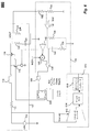
[0040] 以下の説明では、説明の目的のために、多数の例および特定の詳細が、本開示の完全な理解を提供するために記載される。しかしながら、特許請求の範囲において表される本開示が、単独であるいは以下に説明される他の特徴との組み合わせにおいて、これらの例における特徴の一部またはすべてを含み、本明細書で説明される特徴および概念の修正および同等物をさらに含み得ることは、当業者にとって明らかであろう。 [0040] In the following description, for purposes of explanation, numerous examples and specific details are set forth in order to provide a thorough understanding of the present disclosure. However, the disclosure as expressed in the claims, including any or all of the features in these examples, either alone or in combination with other features described below, is described herein. It will be apparent to those skilled in the art that further modifications and equivalents of the features and concepts may be included.
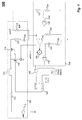
[0041] 図1は、従来のブーストコンバータ100のブロック図を例示する。ブーストコンバータ100は、ブーストコンバータ102、フィードバック回路104、ORゲート106、およびRSフリップフロップ108を備える。ブーストコンバータ102は、入力DC電圧よりも大きい出力DC電圧を備えた電力コンバータである。フィードバック回路104は、出力電圧Voutおよびインダクタ電流を検出し、出力電圧によって設定されたしきい値を超えるインダクタ電流を示す電圧に応答して、トリガ信号を生成する。フィードバック回路104は、ORゲート106の第1の入力にトリガ信号を提供する。ORゲート106の第2の入力は、固定の(この例では50%のデューティで固定の)最大デューティサイクル(ClockMaxD)信号を受信する。ORゲート106は、最大デューティサイクル(ClockMaxD)信号またはトリガ信号のいずれかがハイであることに応答して、RSフリップフロップ108にリセット信号を提供する。RSフリップフロップ108は、外部のコントローラ(図示せず)からのブーストクロック入力またはORゲート106からのリセット信号に応答して、ブーストコンバータ102をスイッチするための制御信号を提供する。
FIG. 1 illustrates a block diagram of a
[0042] ブーストコンバータ102は、入力電圧(VIN)源110、直列抵抗器112、インダクタ114、NMOSトランジスタ116、PMOSトランジスタ118、キャパシタ120、実効直列抵抗器122、および負荷抵抗器124を備える。RSフリップフロップ108からの制御信号に応答して、NMOSトランジスタ116は、インダクタ114にエネルギーを蓄積するためにブーストコンバータ102のオン位相(on phase)中に、接地にインダクタ114を結合する。オン位相中に、RSフリップフロップ108は、PMOSトランジスタ118の電源を切る。ブーストコンバータ102のオフ位相(off phase)中に、RSフリップフロップ108からの制御信号は、インダクタ114に蓄積された電流を負荷抵抗器124に供給するためにNMOSトランジスタ116の電源を切り、PMOSトランジスタ118の電源を入れる。キャパシタ120は、実効直列抵抗器122と直列に存在する理想的なキャパシタとして示される。キャパシタ120は、オフ位相中にインダクタ電流を蓄積する。
The
[0043] フィードバック回路104は、複数の抵抗器132および134、複数のコンパレータ136および138、加算回路140および電流電圧コンバータ142を備える。抵抗器132および134は、出力電圧VOUTと接地との間に直列に結合され、出力電圧VOUTを示すフィードバック電圧をコンパレータ136の反転入力に提供するために電圧分配器として配置される。基準電圧Vrefは、コンパレータ136の非反転入力に提供される。コンパレータ136は、しきい値を超える出力電圧VOUTに応じてコンパレータ138の反転入力に出力電圧しきい値信号を提供し、それは、基準電圧Vrefを超える抵抗器132および134の分配された出力電圧によって表される。抵抗器134および135およびキャパシタ144は、コンパレータ138の出力に対してループ安定性のためのフィルタリングを提供する。NMOSトランジスタ116のソース上の電流は感知され、電圧コンバータ142への電流に提供され、それは、NMOSトランジスタ116を通した電流を示す電圧を加算回路140に提供する。ループ安定性のための補償ランプ信号は、加算回路140に提供され、それは、ランプ電圧信号をコンパレータ138の非反転入力に提供し、それは、トリガ信号をORゲート106の第1の入力に提供する。ORゲート106の動作は、上記で説明されている。
The
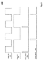
[0044] 図2は、ブーストコンバータ100のタイミング図を例示する。ライン202は、ブーストコンバータ100の外部のコントローラのクロック信号のタイミングを例示する。ライン204は、ライン202に示されるクロック信号から導出された50%のクロック信号のタイミングを例示する。ライン206は、ブーストコンバータ102によってブーストのオンステージ(on-stage)を開始するためのフリップフロップ108をセットするようにORゲート106によってフリップフロップ108に提供されるブーストクロック信号のタイミングを例示する。
FIG. 2 illustrates a timing diagram for the
[0045] ライン208は、ブーストコンバータ102によってブーストのオンステージを終了するためのフリップフロップ108をリセットするようにORゲート106に提供される最大デューティサイクルクロック信号のタイミングを例示する。最大デューティサイクルクロック信号のパルスは固定である。
[0045]
[0046] 図3は、いくつかの実施形態に従ったブーストコンバータ300のブロック図を例示する。ブーストコンバータ300は、ブーストコンバータ102、フィードバック回路104、ORゲート306、RSフリップフロップ308、および最大デューティサイクルリミットジェネレータ310を備える。ブーストコンバータ300は、ブーストコンバータ102以外のブーストコンバータを、またはフィードバック回路104以外のフィードバック回路を含み得る。フィードバック回路104は、ORゲート306の第1の入力にトリガ信号を提供する。ORゲート306の第2の入力は、最大デューティサイクルリミットジェネレータ310から可変である最大デューティサイクル(ClockMaxD)信号を受信する。ORゲート306は、最大デューティサイクル(ClockMaxD)信号またはフィードバック回路104からのトリガ信号のいずれかがハイであることに応答して、RSフリップフロップ308にリセット信号を提供する。RSフリップフロップ308は、外部のコントローラ(図示せず)からのブーストクロック入力またはORゲート306からのリセット信号に応答して、ブーストコンバータ102をスイッチするための制御信号を提供する。
[0046] FIG. 3 illustrates a block diagram of a
[0047] 最大デューティサイクルリミットジェネレータ310は、入力電圧Vinに適応的である。最大デューティサイクルリミットジェネレータ310は、入力電圧Vinに応答して、出力電圧Voutを制御するためにRSフリップフロップ308からブーストコンバータ102への制御信号の最大許容デューティサイクルを調整する。最大デューティサイクルリミットジェネレータ310は、最大デューティサイクルを増加させ、それによって、入力電圧Vinの減少に応答してブーストコンバータ102の許容利得を増加させる。一方では、最大デューティサイクルリミットジェネレータ310は、最大デューティサイクルを減少させ、それによって、入力電圧Vinの増加に応答してブーストコンバータ102の許容利得を低下させる。
[0047] Maximum duty
[0048] 最大デューティサイクルリミットジェネレータ310は、アナログデジタルコンバータ312およびデューティサイクルリミットジェネレータ314を備える。アナログデジタルコンバータ312は、入力電圧Vinをデジタル化し、そのデジタル化された信号をデューティサイクルリミットジェネレータ314に提供する。デューティサイクルリミットジェネレータ314は、最大デューティサイクル(ClockMaxD)信号をORゲート306に提供し、それによって、RSフリップフロップ308をリセットする。以下で説明されるように、図7は、デューティサイクルリミットジェネレータ314の実施形態を示す。
The maximum duty
[0049] いくつかの実施形態において、最大デューティサイクルリミットジェネレータ310は、以下の関係性に基づいて最大デューティサイクルDmaxを生成する:
[0050]
[0049] In some embodiments, the maximum duty
[0050]
![]()
![]()
[0051] ここで、Gは、電圧利得(Vout/Vin)であり、Rnは、NMOSトランジスタ116のインピーダンスであり、Rpは、PMOSトランジスタ118のインピーダンスであり、Reqは、等価負荷抵抗(Vout/Iout)である。
Here, G is a voltage gain (Vout / Vin), Rn is an impedance of the
[0052] いくつかの実施形態において、等価負荷抵抗は、以下のようにPMOSトランジスタ118のインピーダンスとNMOSトランジスタ116のインピーダンスとの間の違いよりもはるかに大きい:
[0053] (Req>>(Rp−Rn)
[0054] この事例において、最大デューティサイクルDmaxは、以下のようになる:
[0055]
[0052] In some embodiments, the equivalent load resistance is much greater than the difference between the impedance of the
[0053] (Req >> (Rp-Rn)
[0054] In this case, the maximum duty cycle Dmax is as follows:
[0055]
![]()
![]()
[0056] 以下に説明される最大デューティサイクルリミットジェネレータはまた、これら関係性に基づいて最大デューティサイクルDmaxを生成し得る。 [0056] The maximum duty cycle limit generator described below may also generate a maximum duty cycle Dmax based on these relationships.
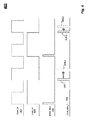
[0057] 図4は、ブーストコンバータ300のタイミング図を例示する。ライン402は、ブーストコンバータ300の外部のコントローラのクロック信号のタイミングを例示する。ライン404は、ライン402に示されるクロック信号から導出された50%のクロック信号のタイミングを例示する。ライン406は、ブーストコンバータ102によってブーストのオンステージを開始するためのフリップフロップ108をセットするようにORゲート306によってフリップフロップ108に提供されるブーストクロック信号のタイミングを例示する。
FIG. 4 illustrates a timing diagram for
[0058] ライン408は、ブーストコンバータ102によってブーストのオンステージを終了するためのフリップフロップ308をリセットするようにORゲート306に提供される最大デューティサイクルクロック信号のタイミングを例示する。最大デューティサイクルリミットジェネレータ310は、デューティサイクルを変更するために、図4の矢印によって示されるように、最大クロックデューティ信号のタイミングを調整する。最大デューティサイクルクロック信号のパルスは可変である。パルス408−1および408−3は、50%のデューティサイクルに対応するパルスを表す。ブーストコンバータ300は、パルス408−1およびパルス408−3とは異なる時間で発生する最大デューティサイクル(ClockMaxD)信号を生成することによってブーストレギュレータ302の最大デューティサイクルを変更することができる。この例において、最大デューティサイクル(ClockMaxD)信号は、パルス408−1よりも遅いパルス408−2、およびパルス408−3よりも遅いパルス408−4として発生する。パルス408−4は、パルス408−3後の時点で発生し、それは、時間パルス480−2がパルス408−1の後に発生することよりも短い。図4には示されていないが、パルス408−2および408−4は、それぞれ、パルス408−1および408−3より前に発生し得る。
[0058]
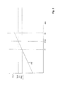
[0059] 図5は、いくつかの実施形態に従ったブーストコンバータ300の適応デューティサイクルのタイミング図を例示する。線502は、経時的なブーストコンバータ300の出力電圧Voutを表す。この例において、線502は、デューティサイクルD1に対してターゲットVoutにある。デューティサイクルがデューティサイクルD2まで増加すると、出力電圧Voutは、最大出力電圧Voutを超える。ブーストコンバータ300は、最大出力電圧Voutにブーストコンバータ300の出力電圧を制限するための最大デューティサイクルDmaxを設定する。
[0059] FIG. 5 illustrates a timing diagram of an adaptive duty cycle of a
[0060] 図6は、いくつかの実施形態に従ったブーストコンバータのブロック図を例示する。ブーストコンバータ600は、ブーストコンバータ102、フィードバック回路104、ORゲート306、RSフリップフロップ308、および最大デューティサイクルリミットジェネレータ610を備える。ブーストコンバータ600は、ブーストコンバータ102以外のブーストコンバータを、またはフィードバック回路104以外のフィードバック回路を含み得る。フィードバック回路104は、ORゲート306の第1の入力にトリガ信号を提供する。ORゲート306の第2の入力は、最大デューティサイクルリミットジェネレータ610から可変である最大デューティサイクル(ClockMaxD)信号を受信する。ORゲート306は、最大デューティサイクル(ClockMaxD)信号またはフィードバック回路104からのトリガ信号のいずれかがハイであることに応答して、RSフリップフロップ308にリセット信号を提供する。RSフリップフロップ308は、外部のコントローラ(図示せず)からのブーストクロック入力またはORゲート306からのリセット信号に応答して、ブーストコンバータ102をスイッチするための制御信号を提供する。
[0060] FIG. 6 illustrates a block diagram of a boost converter according to some embodiments.
[0061] 最大デューティサイクルリミットジェネレータ610は、入力電圧Vinおよび出力電圧Voutに適応的である。最大デューティサイクルリミットジェネレータ610は、入力電圧Vinおよび出力電圧Voutに応答して、出力電圧Voutを制御するためにRSフリップフロップ308からブーストコンバータ102への制御信号の最大デューティサイクルを調整する。最大デューティサイクルリミットジェネレータ610は、最大デューティサイクルを増加させ、それによって、入力電圧Vinの減少または出力電圧Voutにおける減少に応答してブーストコンバータ102の許容利得を増加させる。一方で、最大デューティサイクルリミットジェネレータ610は、最大デューティサイクルを減少させ、それによって、入力電圧Vinの増加または出力電圧Voutにおける増加に応答してブーストコンバータ102の許容利得を減少させる。
[0061] Maximum duty
[0062] 最大デューティサイクルリミットジェネレータ610は、電圧電流コンバータ612、アナログタイマ614、およびデューティサイクルリミットジェネレータ616を備える。電圧電流コンバータ612は、入力電圧Vinをアナログタイマ614に提供される電流に変換する。電流への電圧の変換は、Vout−setを設定する出力電圧の関数であり、それに基づくものであり、それは、出力電圧のプログラムされた値である。アナログタイマ614は、デューティサイクルの開始からの持続時間についてのブーストクロックに関する時間を決定し、その時間をデューティサイクルリミットジェネレータ314に提供する。デューティサイクルリミットジェネレータ616は、しきい値時間以上の時間に応答して最大デューティサイクル(ClockMaxD)信号をORゲート306に提供し、それによって、RSフリップフロップ308をリセットする。以下で説明されるように、図8は、デューティサイクルリミットジェネレータ614の実施形態を示す。
Maximum duty
[0063] 図7は、いくつかの実施形態に従ったデューティサイクルリミッタ700のブロック図を例示する。デューティサイクルリミッタ700は、デューティサイクルリミットジェネレータ314に使用され得る。デューティサイクルリミッタ700は、バッファ702、キャパシタ704、コンパレータ706、基準電圧選択回路708、および遅延回路710を備える。バッファ702は、供給電圧と接地との間に直列に結合された電流枯渇型バッファ716および電流源714を備える。電流枯渇型バッファ716は、ブーストコンバータ102をスイッチするRSフリップフロップ308からの制御信号に応答して、コンパレータ706をトリガするためにコンパレータ706の非反転入力に、およびキャパシタ704を充電するためにキャパシタ704に、電圧信号を提供する。キャパシタ704の充電は、タイマとして機能する。キャパシタ704は、放電回路(図示せず)によって次のデューティサイクルの間、放電されることができる。
[0063] FIG. 7 illustrates a block diagram of a
[0064] 基準電圧選択回路708は、ADC312からの入力電圧コード(VIN ADC CODE)に応答して、コンパレータ706の反転入力に基準電圧を提供する。基準電圧は、入力電圧コードによって示されるような入力電圧VINに反比例する。すなわち、より高い入力電圧は、より低い基準電圧を生成し、その一方で、より低い入力電圧は、より高い基準電圧を生成する。コンパレータ706は、基準電圧選択回路708によって設定される基準電圧を超える電圧を通したキャパシタ704に応答してRSフリップフロップ308をリセットするために遅延回路710に信号を提供する。デフォルトの基準電圧出力および電流源714からの電流の量は、それらを任意の入力クロック周波数に対して動作するよう設定するために電源オン中に調整され得る。
The reference
[0065] 図8は、いくつかの実施形態に従ったデューティサイクルリミッタ800のブロック図を例示する。デューティサイクルリミッタ800は、デューティサイクルリミットジェネレータ314に使用され得る。デューティサイクルリミッタ800は、バッファ802、キャパシタ704、コンパレータ706、および遅延回路710を備える。バッファ802は、供給電圧と接地との間に直列に結合されたバッファ816および可変電流源814を備える。バッファ802はまた、ブーストコンバータ102の出力電圧Voutから導出される、Vout−setを設定する出力電圧に応答して、可変電流源814によって提供された電流を変更するための電圧電流コンバータ818を備える。電圧電流コンバータ818は、Vout−setを設定する出力電圧およびブーストコンバータ102をスイッチするRSフリップフロップ308からの制御信号に応答して、可変電流源814によって提供される適応電流を変更するための制御信号を生成する。バッファ816は、ブーストコンバータ102をスイッチするRSフリップフロップ308からの制御信号に応答して、コンパレータ706をトリガするためにコンパレータ706の非反転入力に、およびキャパシタ704を充電するためにキャパシタ704に、電圧信号を提供する。
[0065] FIG. 8 illustrates a block diagram of a
[0066] キャパシタ704の充電は、タイマとして機能する。キャパシタ704は、放電回路(図示せず)によって次のデューティサイクルの間、放電されることができる。固定の基準電圧Vrefは、コンパレータ706の反転入力に提供される。デューティサイクルリミッタ800において、コンパレータ706に適用される基準電圧Vrefは固定であり、バッファ802によって提供される電流は、入力電圧Vinおよび出力電圧Voutに基づいて可変である。これに対し、デューティサイクルリミッタ800において、コンパレータ706に適用される基準電圧Vrefは、入力電圧Vinに基づいて可変であり、バッファ702によって提供される電圧は、固定である。コンパレータ706は、基準電圧Vrefを超える電圧を通したキャパシタ704に応答して、RSフリップフロップ308をリセットするために遅延回路710に信号を提供する。理解されるように、バッファ802およびコンパレータ706は、同様の機能を提供する他のタイプの回路であり得る。最大デューティサイクル(ClockMaxD)信号は、ブーストレギュレータ102のより滑らかな制御を可能にするように適応的および連続的である。
[0066] Charging of the
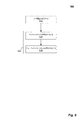
[0067] 図9は、一実施形態に従ったブーストコンバータ102のデューティサイクルを調整するための処理フロー900を例示する簡易図である。
[0067] FIG. 9 is a simplified diagram illustrating a
[0068] 902において、ブーストコンバータ102に提供されるべき入力電圧が受信される。904において、制御信号が入力電圧に応答して生成される。制御信号は、ブースターコンバータ102の出力電圧を制御するようにブーストコンバータ102のデューティサイクルを調整するためのブーストコンバータ102に提供されるべきである。
[0068] At 902, an input voltage to be provided to the
[0069] 904において、制御信号を生成することは、906において、デジタル化された信号がブーストコンバータ102の入力電圧に応答して生成されることを備え得る。908において、ブーストコンバータ102のデューティサイクルを制限するための最大デューティサイクルリミット信号が、デジタル化された信号に応答して生成される。
[0069] Generating the control signal at 904 may comprise, at 906, a digitized signal is generated in response to the input voltage of the
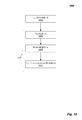
[0070] 図10は、一実施形態に従ったブーストコンバータ102のデューティサイクルを調整するための処理フロー1000を例示する簡易図である。
[0070] FIG. 10 is a simplified diagram illustrating a
[0071] 1002において、ブーストコンバータ102に提供されるべき入力電圧が受信される。1004において、制御信号が、ブーストコンバータ102の出力電圧および入力電圧に応答して生成される。制御信号は、ブースターコンバータ102の出力電圧を制御するようにブーストコンバータ102のデューティサイクルを調整するためのブーストコンバータ102に提供されるべきである。
[0071] At 1002, an input voltage to be provided to the
[0072] 1004において、制御信号を生成することは、1006において、電流がブーストコンバータ102の入力電圧および出力電圧に応答して生成されることを備え得る。1008において、生成された電流が時間測定される。1010において、最大デューティサイクルリミット信号が、時間測定された電流に応答して生成される。
[0072] At 1004, generating the control signal may comprise, at 1006, a current is generated in response to the input voltage and output voltage of the
[0073] 上記の説明は、どのように特定の実施形態の態様が実現され得るかの例と共に、本開示の様々な実施形態を例示する。上記の例は、唯一の実施形態であるように見なされるべきではなく、以下の特許請求の範囲によって定義される特定の実施形態の柔軟性および利点を例示するために提示されている。上記の開示および以下の特許請求の範囲に基づいて、他の配置、実施形態、実現および同等物が、特許請求の範囲によって定義される本開示の範囲から逸脱することなく用いられ得る。 [0073] The above description illustrates various embodiments of the present disclosure, along with examples of how aspects of particular embodiments may be implemented. The above examples should not be considered to be the only embodiments, but are presented to illustrate the flexibility and advantages of certain embodiments as defined by the following claims. Based on the above disclosure and the following claims, other arrangements, embodiments, implementations and equivalents may be used without departing from the scope of this disclosure as defined by the claims.
Claims (20)
前記ブーストコンバータに提供される入力電圧を受信することと、前記入力電圧に応答して、前記ブースターコンバータの前記出力電圧を制御するように前記ブーストコンバータの前記デューティサイクルを調整するための前記ブーストコンバータに提供されるべき制御信号を生成することとを行うように構成されたデューティサイクルリミッタジェネレータ
を備える、制御回路。 A control circuit for adjusting the duty cycle of the boost converter,
The boost converter for receiving an input voltage provided to the boost converter and adjusting the duty cycle of the boost converter to control the output voltage of the boost converter in response to the input voltage A control circuit comprising: a duty cycle limiter generator configured to generate a control signal to be provided to the control circuit.
前記ブーストコンバータの入力電圧に応答して、デジタル化された信号を生成するためのアナログデジタルコンバータと、
前記アナログデジタルコンバータによって生成された前記デジタル化された信号に応答して、前記ブーストコンバータの前記デューティサイクルを制限するために最大デューティサイクル信号を生成するためのデューティサイクルリミットジェネレータと
を備える、請求項1に記載の制御回路。 The duty cycle limiter generator is
An analog-to-digital converter for generating a digitized signal in response to the input voltage of the boost converter;
A duty cycle limit generator for generating a maximum duty cycle signal to limit the duty cycle of the boost converter in response to the digitized signal generated by the analog to digital converter. The control circuit according to 1.
前記ブーストコンバータを制御するために提供されるスイッチング信号に応答して、電流を供給するための電流枯渇型バッファと、
前記電流枯渇型バッファの前記出力と接地との間に結合されたキャパシタと、
前記デジタル化された信号に応答して、基準電圧を生成するための基準電圧選択回路と、
前記キャパシタの両端の電圧および前記基準電圧に応答して、最大デューティサイクル信号を生成するためのコンパレータと
を備える、請求項2に記載の制御回路。 The maximum duty cycle limit generator is:
A current depleted buffer for supplying current in response to a switching signal provided to control the boost converter;
A capacitor coupled between the output of the current depleted buffer and ground;
A reference voltage selection circuit for generating a reference voltage in response to the digitized signal;
A control circuit according to claim 2, comprising: a comparator for generating a maximum duty cycle signal in response to the voltage across the capacitor and the reference voltage.
前記ブーストコンバータの前記入力電圧および出力電圧に応答して、電流を生成するための電圧電流コンバータと、
前記電流を時間測定するためのアナログタイマと、
前記時間測定された電流に応答して、最大デューティサイクル信号を生成するためのデューティサイクルリミットジェネレータと
を備える、請求項1に記載の制御回路。 The maximum duty cycle limit generator is:
A voltage-current converter for generating current in response to the input voltage and output voltage of the boost converter;
An analog timer for time measuring the current;
The control circuit of claim 1, comprising: a duty cycle limit generator for generating a maximum duty cycle signal in response to the timed current.
前記電圧電流コンバータからの前記電流に応答して、バイアス電流を生成するための可変電流源と、
前記ブーストコンバータを制御するために提供されるスイッチング信号および前記バイアス電流に応答して、バッファ電流を供給するためのバッファと、
前記電流枯渇型バッファの前記出力と接地との間に結合されたキャパシタと、
前記キャパシタの両端の電圧および基準電圧に応答して、最大デューティサイクル信号を生成するためのコンパレータと
を備える、請求項5に記載の制御回路。 The maximum duty cycle limit generator is:
A variable current source for generating a bias current in response to the current from the voltage-current converter;
A buffer for supplying a buffer current in response to a switching signal provided to control the boost converter and the bias current;
A capacitor coupled between the output of the current depleted buffer and ground;
6. A control circuit according to claim 5, comprising a comparator for generating a maximum duty cycle signal in response to a voltage across the capacitor and a reference voltage.
前記ブーストコンバータに提供される入力電圧を受信することと、
前記入力電圧に応答して、前記ブースターコンバータの前記出力電圧を制御するように前記ブーストコンバータの前記デューティサイクルを調整するための前記ブーストコンバータに提供すべき制御信号を生成することと
を備える、方法。 A method for adjusting the duty cycle of a boost converter,
Receiving an input voltage provided to the boost converter;
Generating a control signal to be provided to the boost converter for adjusting the duty cycle of the boost converter to control the output voltage of the booster converter in response to the input voltage. .
前記ブーストコンバータの前記入力電圧に応答して、デジタル化された信号を生成することと、
前記デジタル化された信号に応答して、前記ブーストコンバータの前記デューティサイクルを制限するために最大デューティサイクル信号を生成することと
を備える、請求項8に記載の方法。 Generating the control signal is
Generating a digitized signal in response to the input voltage of the boost converter;
Generating a maximum duty cycle signal to limit the duty cycle of the boost converter in response to the digitized signal.
前記ブーストコンバータを制御するために提供されるスイッチング信号に応答して、電流を生成することと、
前記電流を蓄積することと、
前記デジタル化された信号に応答して、基準電圧を生成することと、
最大デューティサイクル信号を生成するために前記蓄積されたバッファ電流と前記基準電圧を比較することと
を備える、請求項9に記載の方法。 Generating the maximum duty cycle signal comprises:
Generating a current in response to a switching signal provided to control the boost converter;
Storing the current;
Generating a reference voltage in response to the digitized signal;
The method of claim 9, comprising comparing the accumulated buffer current to the reference voltage to generate a maximum duty cycle signal.
前記ブーストコンバータの前記入力電圧および出力電圧に応答して、電流を生成することと、
前記生成された電流を時間測定することと、
前記時間測定された電流に応答して、最大デューティサイクル信号を生成することと
を備える、請求項8に記載の方法。 Generating the control signal comprises:
Generating current in response to the input voltage and output voltage of the boost converter;
Timing the generated current;
9. A method according to claim 8, comprising: generating a maximum duty cycle signal in response to the timed current.
前記生成された電流に応答して、バイアス電流を生成することと、
前記ブーストコンバータを制御するために提供されるスイッチング信号および前記バイアス電流に応答してバッファ電流を生成することと、
前記バッファ電流を蓄積することと、
前記蓄積されたバッファ電流を示す電圧および基準電圧に応答して、最大デューティサイクル信号を生成するために前記蓄積されたバッファ電流および基準電圧を比較することと
を備える、請求項12に記載の方法。 Generating a maximum duty cycle signal is
Generating a bias current in response to the generated current;
Generating a buffer current in response to a switching signal provided to control the boost converter and the bias current;
Storing the buffer current;
13. The method of claim 12, comprising: comparing the accumulated buffer current and reference voltage to generate a maximum duty cycle signal in response to a voltage indicative of the accumulated buffer current and a reference voltage. .
前記ブーストコンバータに提供される入力電圧を受信するための手段と、
前記入力電圧に応答して、前記ブースターコンバータの前記出力電圧を制御するように前記ブーストコンバータの前記デューティサイクルを調整するための前記ブーストコンバータに提供すべき制御信号を生成するための手段と
を備える、制御回路。 A control circuit for adjusting the duty cycle of the boost converter,
Means for receiving an input voltage provided to the boost converter;
Means for generating a control signal to be provided to the boost converter for adjusting the duty cycle of the boost converter to control the output voltage of the booster converter in response to the input voltage. , Control circuit.
前記ブーストコンバータの前記入力電圧に応答して、デジタル化された信号を生成するための手段と、
前記デジタル化された信号に応答して、前記ブーストコンバータの前記デューティサイクルを制限するために最大デューティサイクル信号を生成するための手段と
を備える、請求項15に記載の制御回路。 Said means for generating a control signal comprises:
Means for generating a digitized signal in response to the input voltage of the boost converter;
16. A control circuit according to claim 15, comprising means for generating a maximum duty cycle signal to limit the duty cycle of the boost converter in response to the digitized signal.
前記ブーストコンバータを制御するために提供されるスイッチング信号に応答して、電流を生成するための手段と、
前記電流を蓄積するための手段と、
前記デジタル化された信号に応答して、基準電圧を生成するための手段と、
最大デューティサイクル信号を生成するために前記蓄積されたバッファ電流と前記基準電圧を比較するための手段と
を備える、請求項16に記載の制御回路。 The means for generating the maximum duty cycle signal comprises:
Means for generating a current in response to a switching signal provided to control the boost converter;
Means for storing the current;
Means for generating a reference voltage in response to the digitized signal;
17. The control circuit of claim 16, comprising: means for comparing the accumulated buffer current and the reference voltage to generate a maximum duty cycle signal.
前記ブーストコンバータの前記入力電圧および出力電圧に応答して、電流を生成するための手段と、
前記生成された電流を時間測定するための手段と、
前記時間測定された電流に応答して、最大デューティサイクル信号を生成するための手段と
を備える、請求項15に記載の制御回路。 The means for generating the control signal comprises:
Means for generating a current in response to the input voltage and output voltage of the boost converter;
Means for timing the generated current;
16. The control circuit of claim 15, comprising: means for generating a maximum duty cycle signal in response to the timed current.
Applications Claiming Priority (3)
| Application Number | Priority Date | Filing Date | Title |
|---|---|---|---|
| US14/534,034 US10374514B2 (en) | 2014-11-05 | 2014-11-05 | Boost converters having self-adaptive maximum duty-cycle-limit control |
| US14/534,034 | 2014-11-05 | ||
| PCT/US2015/053706 WO2016073090A1 (en) | 2014-11-05 | 2015-10-02 | Boost converters having self-adaptive maximum duty-cycle-limit control |
Publications (2)
| Publication Number | Publication Date |
|---|---|
| JP2017534243A true JP2017534243A (en) | 2017-11-16 |
| JP2017534243A5 JP2017534243A5 (en) | 2018-10-25 |
Family
ID=54330061
Family Applications (1)
| Application Number | Title | Priority Date | Filing Date |
|---|---|---|---|
| JP2017543711A Pending JP2017534243A (en) | 2014-11-05 | 2015-10-02 | Boost converter with self-adaptive maximum duty cycle limit control |
Country Status (6)
| Country | Link |
|---|---|
| US (1) | US10374514B2 (en) |
| EP (1) | EP3216118A1 (en) |
| JP (1) | JP2017534243A (en) |
| KR (1) | KR20170078647A (en) |
| CN (1) | CN107078637A (en) |
| WO (1) | WO2016073090A1 (en) |
Cited By (1)
| Publication number | Priority date | Publication date | Assignee | Title |
|---|---|---|---|---|
| CN112098708A (en) * | 2020-11-23 | 2020-12-18 | 成都市易冲半导体有限公司 | Line voltage information detection circuit and detection method for secondary side PD controller |
Families Citing this family (6)
| Publication number | Priority date | Publication date | Assignee | Title |
|---|---|---|---|---|
| US10270338B2 (en) * | 2017-09-19 | 2019-04-23 | Texas Instruments Incorporated | Shunt regulator including ramp control circuit |
| CN108616209B (en) * | 2018-04-17 | 2019-10-18 | 华南理工大学 | A kind of dynamic regulating method of digital power largest duty cycle value |
| CN109906556B (en) * | 2019-01-22 | 2022-10-04 | 香港应用科技研究院有限公司 | Duty cycle controller with calibration circuit |
| KR102453380B1 (en) | 2019-08-02 | 2022-10-11 | 한국전자통신연구원 | Boost dc-dc converter using dsm, duty ratio controller for the boost dc-dc converter, and a method for configuring the duty ratio controller |
| CN111817562B (en) * | 2020-07-08 | 2021-06-22 | 无锡力芯微电子股份有限公司 | Buck type DC-DC converter |
| CN113258760B (en) * | 2021-05-14 | 2022-11-11 | 珠海格力电器股份有限公司 | Circuit control method and device, electronic equipment and storage medium |
Family Cites Families (13)
| Publication number | Priority date | Publication date | Assignee | Title |
|---|---|---|---|---|
| US6977492B2 (en) | 2002-07-10 | 2005-12-20 | Marvell World Trade Ltd. | Output regulator |
| US6922346B2 (en) | 2003-07-23 | 2005-07-26 | Texas Instruments Incorporated | System and method to limit maximum duty cycle and/or provide a maximum volt-second clamp |
| US6992469B1 (en) | 2004-12-08 | 2006-01-31 | Kiawe Forest, Llc | Digital voltage regulator for DC/DC converters |
| US8059432B2 (en) | 2007-12-12 | 2011-11-15 | Semiconductor Components Industries, Llc. | PWM controller having drive control with input voltage sensing and method therefor |
| JP4577420B2 (en) * | 2008-07-10 | 2010-11-10 | 富士ゼロックス株式会社 | Image processing apparatus and image processing program |
| JP5399734B2 (en) | 2008-09-30 | 2014-01-29 | スパンション エルエルシー | OUTPUT VOLTAGE CONTROL DEVICE, OUTPUT VOLTAGE CONTROL METHOD, AND ELECTRONIC DEVICE |
| TWI371906B (en) | 2009-03-09 | 2012-09-01 | Delta Electronics Inc | Two-stage switching power conversion circuit |
| US8232787B2 (en) | 2009-04-28 | 2012-07-31 | Analog Devices, Inc. | Pulse time detector, a controller for a switched mode power supply, and a switched mode power supply including such a controller |
| US20110140684A1 (en) | 2009-12-10 | 2011-06-16 | Chiccony Power Technology Co., Ltd. | Power controller having externally adjustable duty cycle |
| CN102598866B (en) * | 2010-06-04 | 2014-08-20 | 丰裕国际电子私人有限公司 | Device and method for driving LEDs |
| US8564259B2 (en) * | 2010-11-02 | 2013-10-22 | Intersil Americas LLC | Clock phase shifter for use with buck-boost converter |
| US8970068B2 (en) | 2011-02-10 | 2015-03-03 | Draker, Inc. | Pseudo-random bit sequence generation for maximum power point tracking in photovoltaic arrays |
| US8564267B2 (en) * | 2011-08-26 | 2013-10-22 | Maxim Integrated Products, Inc. | Multi-mode parameter analyzer for power supplies |
-
2014
- 2014-11-05 US US14/534,034 patent/US10374514B2/en not_active Expired - Fee Related
-
2015
- 2015-10-02 KR KR1020177011518A patent/KR20170078647A/en unknown
- 2015-10-02 CN CN201580059849.9A patent/CN107078637A/en active Pending
- 2015-10-02 EP EP15781520.0A patent/EP3216118A1/en not_active Withdrawn
- 2015-10-02 JP JP2017543711A patent/JP2017534243A/en active Pending
- 2015-10-02 WO PCT/US2015/053706 patent/WO2016073090A1/en active Application Filing
Cited By (1)
| Publication number | Priority date | Publication date | Assignee | Title |
|---|---|---|---|---|
| CN112098708A (en) * | 2020-11-23 | 2020-12-18 | 成都市易冲半导体有限公司 | Line voltage information detection circuit and detection method for secondary side PD controller |
Also Published As
| Publication number | Publication date |
|---|---|
| EP3216118A1 (en) | 2017-09-13 |
| KR20170078647A (en) | 2017-07-07 |
| US10374514B2 (en) | 2019-08-06 |
| WO2016073090A1 (en) | 2016-05-12 |
| CN107078637A (en) | 2017-08-18 |
| US20160126839A1 (en) | 2016-05-05 |
Similar Documents
| Publication | Publication Date | Title |
|---|---|---|
| JP2017534243A (en) | Boost converter with self-adaptive maximum duty cycle limit control | |
| US8669744B1 (en) | Adaptive control of switching losses in power converters | |
| US9054596B2 (en) | Device for synchronous DC-DC conversion and synchronous DC-DC converter | |
| US9093899B2 (en) | Timer based PFM exit control method for a boost regulator | |
| US8519691B2 (en) | Current limiting for DC-DC converters | |
| US9529373B2 (en) | Switching regulator and control circuit and control method therefor | |
| US7714547B2 (en) | Method and apparatus for constant on-time switch mode converters | |
| JP6211916B2 (en) | Switching regulator | |
| US9614437B2 (en) | Switching regulator and control circuit and control method therefor | |
| US9716437B2 (en) | Power converter for a switching power supply and manner of operation thereof | |
| TWI679835B (en) | DC-DC converter | |
| US10381927B2 (en) | Pulse-frequency modulation constant on-time with peak-current servo | |
| US9160229B2 (en) | DC-DC converter | |
| US7391195B2 (en) | Self-oscillating boost DC-DC converters with current feedback and digital control algorithm | |
| WO2016077226A1 (en) | Power converter controller with stability compensation | |
| US10948934B1 (en) | Voltage regulator with piecewise linear loadlines | |
| US10060954B2 (en) | Load capacitance determination circuitry and power supply control | |
| CN107317462B (en) | Switch mode power supply control | |
| JP2022549255A (en) | 4-phase buck-boost converter | |
| JP5721403B2 (en) | Buck-boost circuit and buck-boost circuit control method | |
| JP2011155778A (en) | Step-up/down dc-dc converter and switching control circuit | |
| US20220360170A1 (en) | Power delivery control circuit | |
| CN113809916A (en) | Single inductor multiple output DC-DC converter with current control in continuous conduction mode and discontinuous conduction mode | |
| EP1499004B1 (en) | Method for controlling a synchronous rectifier and synchronous rectifier controller | |
| US8120330B1 (en) | Amplitude lock loop for producing constant amplitude oscillator ramp signal |
Legal Events
| Date | Code | Title | Description |
|---|---|---|---|
| A521 | Written amendment |
Free format text: JAPANESE INTERMEDIATE CODE: A523 Effective date: 20180911 |
|
| A621 | Written request for application examination |
Free format text: JAPANESE INTERMEDIATE CODE: A621 Effective date: 20180911 |
|
| A977 | Report on retrieval |
Free format text: JAPANESE INTERMEDIATE CODE: A971007 Effective date: 20190626 |
|
| A131 | Notification of reasons for refusal |
Free format text: JAPANESE INTERMEDIATE CODE: A131 Effective date: 20190716 |
|
| A02 | Decision of refusal |
Free format text: JAPANESE INTERMEDIATE CODE: A02 Effective date: 20200225 |