KR20170078647A - Boost converters having self-adaptive maximum duty-cycle-limit control - Google Patents
Boost converters having self-adaptive maximum duty-cycle-limit control Download PDFInfo
- Publication number
- KR20170078647A KR20170078647A KR1020177011518A KR20177011518A KR20170078647A KR 20170078647 A KR20170078647 A KR 20170078647A KR 1020177011518 A KR1020177011518 A KR 1020177011518A KR 20177011518 A KR20177011518 A KR 20177011518A KR 20170078647 A KR20170078647 A KR 20170078647A
- Authority
- KR
- South Korea
- Prior art keywords
- duty cycle
- boost converter
- current
- generating
- response
- Prior art date
Links
Images


Classifications
-
- H—ELECTRICITY
- H02—GENERATION; CONVERSION OR DISTRIBUTION OF ELECTRIC POWER
- H02M—APPARATUS FOR CONVERSION BETWEEN AC AND AC, BETWEEN AC AND DC, OR BETWEEN DC AND DC, AND FOR USE WITH MAINS OR SIMILAR POWER SUPPLY SYSTEMS; CONVERSION OF DC OR AC INPUT POWER INTO SURGE OUTPUT POWER; CONTROL OR REGULATION THEREOF
- H02M3/00—Conversion of dc power input into dc power output
- H02M3/02—Conversion of dc power input into dc power output without intermediate conversion into ac
- H02M3/04—Conversion of dc power input into dc power output without intermediate conversion into ac by static converters
- H02M3/10—Conversion of dc power input into dc power output without intermediate conversion into ac by static converters using discharge tubes with control electrode or semiconductor devices with control electrode
- H02M3/145—Conversion of dc power input into dc power output without intermediate conversion into ac by static converters using discharge tubes with control electrode or semiconductor devices with control electrode using devices of a triode or transistor type requiring continuous application of a control signal
- H02M3/155—Conversion of dc power input into dc power output without intermediate conversion into ac by static converters using discharge tubes with control electrode or semiconductor devices with control electrode using devices of a triode or transistor type requiring continuous application of a control signal using semiconductor devices only
- H02M3/156—Conversion of dc power input into dc power output without intermediate conversion into ac by static converters using discharge tubes with control electrode or semiconductor devices with control electrode using devices of a triode or transistor type requiring continuous application of a control signal using semiconductor devices only with automatic control of output voltage or current, e.g. switching regulators
- H02M3/157—Conversion of dc power input into dc power output without intermediate conversion into ac by static converters using discharge tubes with control electrode or semiconductor devices with control electrode using devices of a triode or transistor type requiring continuous application of a control signal using semiconductor devices only with automatic control of output voltage or current, e.g. switching regulators with digital control
-
- H—ELECTRICITY
- H02—GENERATION; CONVERSION OR DISTRIBUTION OF ELECTRIC POWER
- H02M—APPARATUS FOR CONVERSION BETWEEN AC AND AC, BETWEEN AC AND DC, OR BETWEEN DC AND DC, AND FOR USE WITH MAINS OR SIMILAR POWER SUPPLY SYSTEMS; CONVERSION OF DC OR AC INPUT POWER INTO SURGE OUTPUT POWER; CONTROL OR REGULATION THEREOF
- H02M3/00—Conversion of dc power input into dc power output
- H02M3/02—Conversion of dc power input into dc power output without intermediate conversion into ac
- H02M3/04—Conversion of dc power input into dc power output without intermediate conversion into ac by static converters
- H02M3/10—Conversion of dc power input into dc power output without intermediate conversion into ac by static converters using discharge tubes with control electrode or semiconductor devices with control electrode
- H02M3/145—Conversion of dc power input into dc power output without intermediate conversion into ac by static converters using discharge tubes with control electrode or semiconductor devices with control electrode using devices of a triode or transistor type requiring continuous application of a control signal
- H02M3/155—Conversion of dc power input into dc power output without intermediate conversion into ac by static converters using discharge tubes with control electrode or semiconductor devices with control electrode using devices of a triode or transistor type requiring continuous application of a control signal using semiconductor devices only
- H02M3/156—Conversion of dc power input into dc power output without intermediate conversion into ac by static converters using discharge tubes with control electrode or semiconductor devices with control electrode using devices of a triode or transistor type requiring continuous application of a control signal using semiconductor devices only with automatic control of output voltage or current, e.g. switching regulators
- H02M3/158—Conversion of dc power input into dc power output without intermediate conversion into ac by static converters using discharge tubes with control electrode or semiconductor devices with control electrode using devices of a triode or transistor type requiring continuous application of a control signal using semiconductor devices only with automatic control of output voltage or current, e.g. switching regulators including plural semiconductor devices as final control devices for a single load
-
- H—ELECTRICITY
- H02—GENERATION; CONVERSION OR DISTRIBUTION OF ELECTRIC POWER
- H02M—APPARATUS FOR CONVERSION BETWEEN AC AND AC, BETWEEN AC AND DC, OR BETWEEN DC AND DC, AND FOR USE WITH MAINS OR SIMILAR POWER SUPPLY SYSTEMS; CONVERSION OF DC OR AC INPUT POWER INTO SURGE OUTPUT POWER; CONTROL OR REGULATION THEREOF
- H02M1/00—Details of apparatus for conversion
- H02M1/0003—Details of control, feedback or regulation circuits
- H02M1/0012—Control circuits using digital or numerical techniques
-
- H—ELECTRICITY
- H02—GENERATION; CONVERSION OR DISTRIBUTION OF ELECTRIC POWER
- H02M—APPARATUS FOR CONVERSION BETWEEN AC AND AC, BETWEEN AC AND DC, OR BETWEEN DC AND DC, AND FOR USE WITH MAINS OR SIMILAR POWER SUPPLY SYSTEMS; CONVERSION OF DC OR AC INPUT POWER INTO SURGE OUTPUT POWER; CONTROL OR REGULATION THEREOF
- H02M1/00—Details of apparatus for conversion
- H02M1/0003—Details of control, feedback or regulation circuits
- H02M1/0016—Control circuits providing compensation of output voltage deviations using feedforward of disturbance parameters
- H02M1/0022—Control circuits providing compensation of output voltage deviations using feedforward of disturbance parameters the disturbance parameters being input voltage fluctuations
-
- H02M2001/0012—
-
- H02M2001/0022—
Abstract
일 실시예에서, 제어 회로는, 부스트 컨버터의 듀티 사이클을 조절하고, 그리고 입력 전압에 대한 응답으로 부스트 컨버터의 출력 전압을 제어하도록 부스트 컨버터의 듀티 사이클을 조절하기 위해 부스트 컨버터에 제공될 제어 신호를 발생시키도록 그리고 부스트 컨버터에 제공되는 입력 전압을 수신하도록 구성되는 듀티 사이클 리미터 발생기를 포함한다. 일 실시예에서, 최대 듀티 사이클 리미트 발생기는 부스트 컨버터의 출력 전압에 대한 응답으로 최대 듀티 사이클 신호를 추가로 발생시킨다. In one embodiment, the control circuit includes a control signal to adjust the duty cycle of the boost converter, and to control the duty cycle of the boost converter to control the output voltage of the boost converter in response to the input voltage And a duty cycle limiter generator configured to receive the input voltage provided to the boost converter. In one embodiment, the maximum duty cycle limit generator further generates a maximum duty cycle signal in response to the output voltage of the boost converter.
Description
관련 출원들에 대한 상호 참조Cross reference to related applications
[0001] 35 U.S.C. §119(e)에 따라, 본 출원은, 2014년 11월 5일자로 출원된 U.S 출원 제14/534,034호의 출원일의 이익을 주장하고 이를 우선권으로 주장하며, 그 내용은 모든 목적을 위해 그 전체가 참조로 본원에 포함된다. [0001] 35 U.S.C. In accordance with §119 (e), the present application claims and claims priority from the filing date of U.S. Serial No. 14 / 534,034, filed November 5, 2014, which is hereby incorporated by reference in its entirety for all purposes Which is incorporated herein by reference.
[0002] 본 개시내용은, 부스트 컨버터들, 특히, 자체-적응형 최대 듀티-사이클-리미트 제어를 갖는 부스트 컨버터들에 관한 것이다. [0002] The present disclosure relates to boost converters, and in particular to boost converters with self-adaptive maximum duty-cycle-limit control.
[0003] 본원에 달리 명시되지 않는 한, 이 섹션에서 설명된 접근방식들은 이 섹션에 포함됨으로 인해 종래 기술이 되는 것으로 인정되지는 않는다. [0003] Unless otherwise specified herein, the approaches described in this section are not admitted to be prior art due to their inclusion in this section.
[0004] 부스트 컨버터들은, 고정 듀티 사이클에서 부스트 컨버터를 스위칭함으로써 입력 전압(Vin) 보다 더 높은 출력 전압(Vout)을 발생시킨다. 부스트 컨버터가 더 낮은 입력 전압들에서 더 높은 출력 부하들을 구동할 때, 부스트 컨버터에 의한 허용가능한 규제를 달성하는 것은 어려울 수 있다. 이러한 문제는, 부스트 컨버터의 이득이 높고 큰 변동을 가질 때 종종 발생한다. 예컨대, 입력 전압(Vin)은 2.5볼트 내지 4.7볼트로 변할 수 있는 반면, 출력 전압(Vout)은 10볼트에 있다(부스트 컨버터에 의해 2.12 내지 4.0의 이득을 생성한다). [0004] The boost converters generate an output voltage Vout that is higher than the input voltage Vin by switching the boost converter in a fixed duty cycle. When the boost converter drives higher output loads at lower input voltages, it may be difficult to achieve acceptable regulation by the boost converter. This problem often occurs when the gain of the boost converter is high and has large variations. For example, the input voltage Vin may vary from 2.5 volts to 4.7 volts, while the output voltage Vout is 10 volts (produces a gain of 2.12 to 4.0 by the boost converter).
[0005] 허용가능한 신뢰도 및 허용가능한 스파이크 레벨들을 달성하는 것은, 입력 전압(Vin)이 타겟 출력 전압(Vout)에 매우 가까울 때에는 어려울 수 있다. 이러한 예시에서, 듀티 사이클은 더 낮아야만 한다. 듀티 사이클이 고정되기 때문에, 최대 듀티 사이클에 의해 정의되는 가능한 최대 출력 전압은 부스트 컨버터의 타겟 출력 전압보다 훨씬 더 높을 수 있다. [0005] Achieving acceptable reliability and acceptable spike levels may be difficult when the input voltage Vin is very close to the target output voltage Vout. In this example, the duty cycle must be lower. Because the duty cycle is fixed, the maximum possible output voltage defined by the maximum duty cycle may be much higher than the target output voltage of the boost converter.
[0006] 본 개시내용은 자체-적응형 최대 듀티-사이클-리미트 제어를 갖는 부스트 컨버터들을 설명한다. [0006] This disclosure describes boost converters with self-adaptive maximum duty-cycle-limit control.
[0007] 일 실시예에서, 제어 회로는 부스트 컨버터의 듀티 사이클을 조절한다. 제어 회로는, 부스트 컨버터에 제공되는 입력 전압을 수신하고, 입력 전압에 대한 응답으로 부스트 컨버터의 출력 전압을 제어하도록 부스트 컨버터의 듀티 사이클을 조절하기 위해 부스트 컨버터에 제공될 제어 신호를 발생시키도록 구성되는 듀티 사이클 리미터 발생기(duty cycle limiter generator)를 포함한다. [0007] In one embodiment, the control circuit regulates the duty cycle of the boost converter. The control circuit is configured to receive the input voltage provided to the boost converter and to generate a control signal to be provided to the boost converter to adjust the duty cycle of the boost converter to control the output voltage of the boost converter in response to the input voltage And a duty cycle limiter generator.
[0008] 일 실시예에서, 듀티 사이클 리미터 발생기는, 부스트 컨버터의 입력 전압에 대한 응답으로 디지털화된 신호를 발생시키기 위한 아날로그-디지털 컨버터; 및 아날로그-디지털 컨버터에 의해 발생된 디지털화된 신호에 대한 응답으로 부스트 컨버터의 듀티 사이클을 제한하도록 최대 듀티 사이클 신호를 발생시키기 위한 최대 듀티 사이클 리미트 발생기를 포함한다. [0008] In one embodiment, the duty cycle limiter generator comprises: an analog-to-digital converter for generating a digitized signal in response to an input voltage of the boost converter; And a maximum duty cycle limit generator for generating a maximum duty cycle signal to limit the duty cycle of the boost converter in response to the digitized signal generated by the analog-to-digital converter.
[0009] 일 실시예에서, 최대 듀티 사이클 리미트 발생기는, 부스트 컨버터를 제어하도록 제공된 스위칭 신호에 대한 응답으로 전류를 제공하기 위한 전류 제한 버퍼(current starved buffer); 전류 제한 버퍼의 출력과 접지 사이에 커플링된 커패시터; 디지털화된 신호에 대한 응답으로 기준 전압을 발생시키기 위한 기준 전압 선택 회로; 및 커패시터 양단의 전압 및 기준 전압에 대한 응답으로 최대 듀티 사이클 신호를 발생시키기 위한 비교기를 포함한다. [0009] In one embodiment, the maximum duty cycle limit generator includes: a current starved buffer for providing current in response to a switching signal provided to control the boost converter; A capacitor coupled between the output of the current limit buffer and ground; A reference voltage selection circuit for generating a reference voltage in response to the digitized signal; And a comparator for generating a maximum duty cycle signal in response to a voltage and a reference voltage across the capacitor.
[0010] 일 실시예에서, 최대 듀티 사이클 리미트 발생기는 부스트 컨버터의 출력 전압에 대한 응답으로 최대 듀티 사이클 신호를 추가로 발생시킨다. [0010] In one embodiment, the maximum duty cycle limit generator further generates a maximum duty cycle signal in response to the output voltage of the boost converter.
[0011] 일 실시예에서, 최대 듀티 사이클 리미트 발생기는: 부스트 컨버터의 입력 전압 및 출력 전압에 대한 응답으로 전류를 발생시키기 위한 전압-전류 컨버터; 전류를 타이밍하기 위한 아날로그 타이머; 및 타이밍된 전류에 대한 응답으로 최대 듀티 사이클 신호를 발생시키기 위한 듀티 사이클 리미트 발생기를 포함한다. [0011] In one embodiment, the maximum duty cycle limit generator comprises: a voltage-to-current converter for generating a current in response to an input voltage and an output voltage of the boost converter; An analog timer for timing current; And a duty cycle limit generator for generating a maximum duty cycle signal in response to the timed current.
[0012] 일 실시예에서, 아날로그 타이머는 전류를 저장하기 위해 전압-전류 컨버터의 출력에 커플링된 커패시터이다. [0012] In one embodiment, the analog timer is a capacitor coupled to the output of the voltage-current converter to store the current.
[0013] 일 실시예에서, 최대 듀티 사이클 리미트 발생기는, 전압-전류 컨버터로부터의 전류에 대한 응답으로 바이어스 전류를 발생시키기 위한 가변 전류원; 부스트 컨버터를 제어하도록 제공된 스위칭 신호 및 바이어스 전류에 대한 응답으로 버퍼 전류를 제공하기 위한 버퍼; 전류 제한 버퍼의 출력과 접지 사이에 커플링된 커패시터; 및 커패시터 양단의 전압 및 기준 전압에 대한 응답으로 최대 듀티 사이클 신호를 발생시키기 위한 비교기를 포함한다. [0013] In one embodiment, the maximum duty cycle limit generator comprises: a variable current source for generating a bias current in response to a current from the voltage-current converter; A buffer for providing a buffer current in response to a switching signal and a bias current provided to control the boost converter; A capacitor coupled between the output of the current limit buffer and ground; And a comparator for generating a maximum duty cycle signal in response to a voltage and a reference voltage across the capacitor.
[0014] 일 실시예에서, 방법은, 부스트 컨버터의 듀티 사이클을 조절하기 위한 것이다. 방법은, 부스트 컨버터에 제공되는 입력 전압을 수신하는 단계; 및 입력 전압에 대한 응답으로 부스트 컨버터의 출력 전압을 제어하도록 부스트 컨버터의 듀티 사이클을 조절하기 위해 부스트 컨버터에 제공하기 위한 제어 신호를 발생시키는 단계를 포함한다. [0014] In one embodiment, the method is for regulating the duty cycle of the boost converter. The method includes receiving an input voltage provided to the boost converter; And generating a control signal for providing to the boost converter to adjust the duty cycle of the boost converter to control the output voltage of the boost converter in response to the input voltage.
[0015] 일 실시예에서, 제어 신호를 발생시키는 단계는, 부스트 컨버터의 입력 전압에 대한 응답으로 디지털화된 신호를 발생시키는 단계; 및 디지털화된 신호에 대한 응답으로 부스트 컨버터의 듀티 사이클을 제한하기 위해 최대 듀티 사이클 신호를 발생시키는 단계를 포함한다. [0015] In one embodiment, generating the control signal comprises: generating a digitized signal in response to an input voltage of the boost converter; And generating a maximum duty cycle signal to limit the duty cycle of the boost converter in response to the digitized signal.
[0016] 일 실시예에서, 최대 듀티 사이클 신호를 발생시키는 단계는, 부스트 컨버터를 제어하도록 제공된 스위칭 신호에 대한 응답으로 전류를 발생시키는 단계; 전류를 저장하는 단계; 디지털화된 신호에 대한 응답으로 기준 전압을 발생시키는 단계; 및 최대 듀티 사이클 신호를 발생시키기 위해 기준 전압과 저장된 버퍼 전류를 비교하는 단계를 포함한다. [0016] In one embodiment, generating the maximum duty cycle signal comprises: generating a current in response to a switching signal provided to control the boost converter; Storing a current; Generating a reference voltage in response to the digitized signal; And comparing the stored buffer current with a reference voltage to generate a maximum duty cycle signal.
[0017] 일 실시예에서, 제어 신호를 발생시키는 단계는, 부스트 컨버터의 입력 전압 및 출력 전압에 대한 응답으로 제어 신호를 발생시키는 단계를 더 포함한다. [0017] In one embodiment, generating the control signal further comprises generating a control signal in response to an input voltage and an output voltage of the boost converter.
[0018] 일 실시예에서, 제어 신호를 발생시키는 단계는, 부스트 컨버터의 입력 전압 및 출력 전압에 대한 응답으로 전류를 발생시키는 단계; 발생된 전류를 타이밍하는 단계; 및 타이밍된 전류에 대한 응답으로 최대 듀티 사이클 신호를 발생시키는 단계를 포함한다. [0018] In one embodiment, generating the control signal comprises: generating a current in response to an input voltage and an output voltage of the boost converter; Timing the generated current; And generating a maximum duty cycle signal in response to the timed current.
[0019] 일 실시예에서, 발생된 전류를 타이밍하는 단계는, 발생된 전류의 전하를 저장하는 단계를 포함한다. [0019] In one embodiment, timing the generated current includes storing the charge of the generated current.
[0020] 일 실시예에서, 최대 듀티 사이클 신호를 발생시키는 단계는, 발생된 전류에 대한 응답으로 바이어스 전류를 발생시키는 단계; 부스트 컨버터를 제어하도록 제공된 스위칭 신호 및 바이어스 전류에 대한 응답으로 버퍼 전류를 발생시키는 단계; 버퍼 전류를 저장하는 단계; 및 저장된 버퍼 전류를 나타내는 전압 및 기준 전압에 대한 응답으로 최대 듀티 사이클 신호를 발생시키기 위해 저장된 버퍼 전류와 기준 전압을 비교하는 단계를 포함한다. [0020] In one embodiment, generating the maximum duty cycle signal comprises: generating a bias current in response to the generated current; Generating a buffer current in response to a switching signal and a bias current provided to control the boost converter; Storing a buffer current; And comparing the stored buffer current and a reference voltage to generate a maximum duty cycle signal in response to the voltage and reference voltage representing the stored buffer current.
[0021] 일 실시예에서, 제어 회로는 부스트 컨버터의 듀티 사이클을 조절하기 위한 것이다. 제어 회로는, 부스트 컨버터에 제공되는 입력 전압을 수신하기 위한 수단; 및 입력 전압에 대한 응답으로 부스트 컨버터의 출력 전압을 제어하도록 부스트 컨버터의 듀티 사이클을 조절하기 위해 부스트 컨버터에 제공하기 위한 제어 신호를 발생시키기 위한 수단을 포함한다. [0021] In one embodiment, the control circuit is for regulating the duty cycle of the boost converter. The control circuit comprising: means for receiving an input voltage provided to the boost converter; And means for generating a control signal for providing to the boost converter to adjust the duty cycle of the boost converter to control the output voltage of the boost converter in response to the input voltage.
[0022] 일 실시예에서, 제어 신호를 발생시키기 위한 수단은, 부스트 컨버터의 입력 전압에 대한 응답으로 디지털화된 신호를 발생시키기 위한 수단; 및 디지털화된 신호에 대한 응답으로 부스트 컨버터의 듀티 사이클을 제한하기 위해 최대 듀티 사이클 신호를 발생시키기 위한 수단을 포함한다. [0022] In one embodiment, the means for generating a control signal comprises means for generating a digitized signal in response to an input voltage of the boost converter; And means for generating a maximum duty cycle signal to limit the duty cycle of the boost converter in response to the digitized signal.
[0023] 일 실시예에서, 최대 듀티 사이클 신호를 발생시키기 위한 수단은, 부스트 컨버터를 제어하도록 제공된 스위칭 신호에 대한 응답으로 전류를 발생시키기 위한 수단; 전류를 저장하기 위한 수단; 디지털화된 신호에 대한 응답으로 기준 전압을 발생시키기 위한 수단; 및 최대 듀티 사이클 신호를 발생시키기 위해 기준 전압과 저장된 버퍼 전류를 비교하기 위한 수단을 포함한다. [0023] In one embodiment, the means for generating a maximum duty cycle signal comprises means for generating a current in response to a switching signal provided to control the boost converter; Means for storing current; Means for generating a reference voltage in response to the digitized signal; And means for comparing the stored buffer current with a reference voltage to generate a maximum duty cycle signal.
[0024] 일 실시예에서, 제어 신호를 발생시키기 위한 수단은, 부스트 컨버터의 입력 전압 및 출력 전압에 대한 응답으로 제어 신호를 발생시키기 위한 수단을 더 포함한다. [0024] In one embodiment, the means for generating a control signal further comprises means for generating a control signal in response to an input voltage and an output voltage of the boost converter.
[0025] 일 실시예에서, 제어 신호를 발생시키기 위한 수단은, 부스트 컨버터의 입력 전압 및 출력 전압에 대한 응답으로 전류를 발생시키기 위한 수단; 발생된 전류를 타이밍하기 위한 수단; 및 타이밍된 전류에 대한 응답으로 최대 듀티 사이클 신호를 발생시키기 위한 수단을 포함한다. [0025] In one embodiment, the means for generating a control signal comprises means for generating a current in response to an input voltage and an output voltage of the boost converter; Means for timing the generated current; And means for generating a maximum duty cycle signal in response to the timed current.
[0026] 일 실시예에서, 발생된 전류를 타이밍하기 위한 수단은, 발생된 전류의 전하를 저장하기 위한 수단을 포함한다. [0026] In one embodiment, the means for timing the generated current comprises means for storing the charge of the generated current.
[0027] 일 실시예에서, 최대 듀티 사이클 신호를 발생시키기 위한 수단은, 발생된 전류에 대한 응답으로 바이어스 전류를 발생시키기 위한 수단; 부스트 컨버터를 제어하도록 제공된 스위칭 신호 및 바이어스 전류에 대한 응답으로 버퍼 전류를 발생시키기 위한 수단; 버퍼 전류를 저장하기 위한 수단; 및 저장된 버퍼 전류를 나타내는 전압 및 기준 전압에 대한 응답으로 최대 듀티 사이클 신호를 발생시키기 위해 저장된 버퍼 전류와 기준 전압을 비교하기 위한 수단을 포함한다. [0027] In one embodiment, the means for generating a maximum duty cycle signal comprises means for generating a bias current in response to the generated current; Means for generating a buffer current in response to a switching signal and a bias current provided to control the boost converter; Means for storing a buffer current; And means for comparing the stored buffer current and the reference voltage to generate a maximum duty cycle signal in response to the voltage and reference voltage representing the stored buffer current.
[0028] 후술하는 상세한 설명 및 첨부 도면들은 본 개시내용의 속성 및 이점들의 더 나은 이해를 제공한다. [0028] The following detailed description and the annexed drawings provide a better understanding of the nature and advantages of the present disclosure.
[0029]
후술하는 특히 도면들에 대한 논의와 관련하여, 도시된 특정사항들이 예시적인 논의의 목적을 위한 예시들을 나타내고, 본 개시내용의 원리들 및 개념적 양상들의 설명을 제공하기 위해 제시되는 것이 강조된다. 이와 관련하여, 본 개시내용의 기본적인 이해를 위해 필수적인 것 이외의 구현 세부사항들을 나타내기 위한 어떠한 시도도 이루어지지 않는다. 도면들과 관련하여 후술하는 논의는, 본 발명에 따른 실시예들이 어떻게 실행되는지를 당업자들에게 명백하게 한다. 첨부 도면들에서:
[0030]
도 1은 종래의 부스트 컨버터의 블록도를 도시한다.
[0031]
도 2는 도 1의 종래의 부스트 컨버터의 타이밍도를 도시한다.
[0032]
도 3은 일부 실시예들에 따른 부스트 컨버터의 블록도를 도시한다.
[0033]
도 4는 일부 실시예들에 따른 도 3의 부스트 컨버터의 타이밍도를 도시한다.
[0034]
도 5는 일부 실시예들에 따른 도 3의 부스트 컨버터의 적응형 듀티 사이클의 타이밍도를 도시한다.
[0035]
도 6은 일부 실시예들에 따른 부스트 컨버터의 블록도를 도시한다.
[0036]
도 7은 일부 실시예들에 따른 듀티 사이클 리미터의 블록도를 도시한다.
[0037]
도 8은 일부 실시예들에 따른 듀티 사이클 리미터의 블록도를 도시한다.
[0038]
도 9는 일부 실시예들에 따라 부스트 컨버터의 듀티 사이클을 조절하기 위한 프로세스 흐름을 도시하는 간략화된 도면이다.
[0039]
도 10는 일부 다른 실시예들에 따라 부스트 컨버터의 듀티 사이클을 조절하기 위한 프로세스 흐름을 도시하는 간략화된 도면이다. [0029] In connection with the discussion of the figures specifically set forth below, it should be emphasized that the specifics indicated represent examples for the purposes of illustrative discussion, and are presented to provide an understanding of the principles and conceptual aspects of the present disclosure do. In this regard, no attempt is made to represent implementation details other than those necessary for a basic understanding of the present disclosure. The discussion that follows with reference to the drawings makes it clear to those skilled in the art how the embodiments according to the invention are implemented. In the accompanying drawings:
[0030] FIG. 1 shows a block diagram of a conventional boost converter.
[0031] FIG. 2 shows a timing diagram of the conventional boost converter of FIG.
[0032] FIG. 3 illustrates a block diagram of a boost converter in accordance with some embodiments.
[0033] FIG. 4 shows a timing diagram of the boost converter of FIG. 3 in accordance with some embodiments.
[0034] FIG. 5 illustrates a timing diagram of an adaptive duty cycle of the boost converter of FIG. 3 in accordance with some embodiments.
[0035] FIG. 6 illustrates a block diagram of a boost converter in accordance with some embodiments.
[0036] FIG. 7 illustrates a block diagram of a duty cycle limiter in accordance with some embodiments.
[0037] Figure 8 illustrates a block diagram of a duty cycle limiter in accordance with some embodiments.
[0038] FIG. 9 is a simplified diagram illustrating a process flow for adjusting the duty cycle of a boost converter in accordance with some embodiments.
[0039] FIG. 10 is a simplified diagram illustrating a process flow for adjusting the duty cycle of a boost converter in accordance with some other embodiments.
[0040] 이하의 설명에서, 설명의 목적들을 위해, 본 개시내용의 완전한 이해를 제공하기 위해 다수의 예시들 및 특정 세부사항들이 설명된다. 그러나, 청구항들에 나타낸 것과 같은 본 개시내용은 몇몇 또는 모든 특징들을 이들의 예시들에서만 단독으로 또는 이하 설명된 다른 특징들과 조합하여 포함할 수 있고, 본원에 설명된 특징들 및 개념들의 변형들 및 등가물들을 추가로 포함할 수 있다는 점이 당업자에게 명백하게 될 것이다. [0040] In the following description, for purposes of explanation, numerous illustrations and specific details are set forth in order to provide a thorough understanding of the present disclosure. It should be understood, however, that the present disclosure, as set forth in the claims, may include some or all of the features singly or in combination with other features described below in these examples, and variations of the features and concepts described herein And equivalents thereof, as will be apparent to those skilled in the art.
[0041]
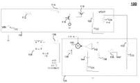
도 1은 종래의 부스트 컨버터(100)의 블록도를 도시한다. 부스트 컨버터(100)는, 부스트 컨버터(102), 피드백 회로(104), OR 게이트(106), 및 RS 플립-플롭(108)을 포함한다. 부스트 컨버터(102)는 입력 DC 전압보다 더 큰 출력 DC 전압을 갖는 전력 컨버터이다. 피드백 회로(104)는, 출력 전압(Vout) 및 인덕터 전류를 검출하고, 출력 전압에 의해 설정된 임계치를 초과하는 인덕터 전류를 나타내는 전압에 대한 응답으로 트리거 신호를 발생시킨다. 피드백 회로(104)는 OR 게이트(106)의 제 1 입력에 그 트리거 신호를 제공한다. OR 게이트(106)의 제 2 입력은, 고정된(이 예시에서는, 50% 듀티에 고정된) 최대 듀티 사이클(ClockMaxD) 신호를 수신한다. OR 게이트(106)는, 트리거 신호 또는 최대 듀티 사이클(ClockMaxD) 신호가 하이인 것에 대한 응답으로, 리셋 신호를 RS 플립-플롭(108)에 제공한다. RS 플립-플롭(108)은 외부 제어기(미도시)로부터의 부스트 클록 입력 또는 OR 게이트(106)로부터의 리셋 신호에 대한 응답으로 부스트 컨버터(102)를 스위칭하기 위한 제어 신호를 제공한다. [0041]
Figure 1 shows a block diagram of a
[0042]
부스트 컨버터(102)는, 입력 전압(VIN) 소스(110), 직렬 저항기(112), 인덕터(114), NMOS 트랜지스터(116), PMOS 트랜지스터(118), 커패시터(120), 유효 직렬 저항기(122), 및 부하 저항기(124)를 포함한다. RS 플립-플롭(108)으로부터의 제어 신호에 대한 응답으로, NMOS 트랜지스터(116)는 인덕터(114) 내에 에너지를 저장하기 위해 부스트 컨버터(102)의 온 페이즈(on phase) 동안 접지에 인덕터(114)를 커플링한다. 온 페이즈 동안, RS 플립-플롭(108)은 PMOS 트랜지스터(118)를 턴 오프한다. 부스트 컨버터(102)의 오프 페이즈 동안, RS 플립-플롭(108)으로부터의 제어 신호는, NMOS 트랜지스터(116)를 턴 오프하고 그리고 PMOS 트랜지스터(118)를 턴 온하여 인덕터(114)에 저장된 전류를 부하 저항기(124)에 제공한다. 커패시터(120)는 유효 직렬 저항기(122)과 직렬로 이상적인 커패시터로서 도시된다. 커패시터(120)는 오프 페이즈 동안 인덕터 전류를 저장한다. [0042]
The
[0043]
피드백 회로(104)는, 복수의 저항기들(132 및 134), 복수의 비교기들(136 및 138), 합산 회로(140), 및 전류-전압 컨버터(142)를 포함한다. 저항기들(132 및 134)은, 출력 전압(VOUT)과 접지 사이에 직렬로 커플링되고, 출력 전압(VOUT)을 나타내는 피드백 전압을 비교기(136)의 반전 입력에 제공하기 위해 전압 분배기로서 배열된다. 기준 전압(Vref)은 비교기(136)의 비-반전 입력에 제공된다. 비교기(136)는, 기준 전압(Vref)을 초과하는 저항기들(132 및 134)의 분할된 출력 전압으로 표현되는, 임계치를 초과하는 출력 전압(VOUT)에 대한 응답으로 비교기(138)의 반전 입력에 출력 전압 임계 신호를 제공한다. 저항기들(134 및 135) 및 커패시터(144)는 비교기(138)의 출력에 루프 안정성을 위한 필터링을 제공한다. NMOS 트랜지스터(116)의 소스 상의 전류는, 감지되어 NMOS 트랜지스터(116)를 통해 합산회로(140)로 흐르는 전류를 나타내는 전압을 제공하는 전류-전압 컨버터(142)에 제공된다. 보상 램프 신호는, 루프 안정성을 위해, OR 게이트(106)의 제 1 입력에 트리거 신호를 제공하는 비교기(138)의 비-반전 입력에 램프 전압 신호를 제공하는 합산 회로(140)에 제공된다. OR 게이트(106)의 동작이 위에 설명된다. [0043]
The
[0044]
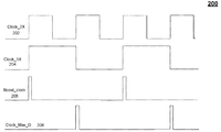
도 2는 부스트 컨버터(100)의 타이밍도를 도시한다. 라인(202)은 부스트 컨버터(100)의 외부 제어기의 클록 신호의 타이밍을 도시한다. 라인(204)은 라인(202)에 도시된 클록 신호로부터 도출된 50% 클록 신호의 타이밍을 도시한다. 라인(206)은 부스트 컨버터(102)에 의한 부스트의 온-스테이지를 시작하도록 플립-플롭(108)을 설정하기 위해 OR 게이트(106)에 의해 플립-플롭(108)에 제공된 부스트 클록 신호의 타이밍을 도시한다. [0044]
2 shows a timing diagram of the
[0045]
라인(208)은 부스트 컨버터(102)에 의한 부스트의 온-스테이지를 종료하도록 플립-플롭(108)을 리셋하기 위해 OR 게이트(106)에 제공된 최대 듀티 사이클 클록 신호의 타이밍을 도시한다. 최대 듀티 사이클 클록 신호의 펄스는 고정된다. [0045]
[0046]
도 3은 일부 실시예들에 따른 부스트 컨버터(300)의 블록도를 도시한다. 부스트 컨버터(300)는, 부스트 컨버터(102), 피드백 회로(104), OR 게이트(306), RS 플립-플롭(308), 및 최대 듀티 사이클 리미트 발생기(310)를 포함한다. 부스트 컨버터(300)는, 부스트 컨버터(102) 이외의 부스트 컨버터들을 포함할 수 있거나 또는 피드백 회로(104) 이외의 피드백 회로를 포함할 수 있다. 피드백 회로(104)는 OR 게이트(306)의 제 1 입력에 그 트리거 신호를 제공한다. OR 게이트(306)의 제 2 입력은, 최대 듀티 사이클 리미트 발생기(310)로부터 가변적인 최대 듀티 사이클(ClockMaxD) 신호를 수신한다. OR 게이트(306)는, 피드백 회로(104)로부터의 트리거 신호 또는 최대 듀티 사이클(ClockMaxD) 신호가 하이(high)인 것에 대한 응답으로 RS 플립-플롭(308)에 리셋 신호를 제공한다. RS 플립-플롭(308)은 외부 제어기(미도시)로부터의 부스트 클록 입력 또는 OR 게이트(306)로부터의 리셋 신호에 대한 응답으로 부스트 컨버터(102)를 스위칭하기 위한 제어 신호를 제공한다. [0046]
FIG. 3 shows a block diagram of
[0047]
최대 듀티 사이클 리미트 발생기(310)는 입력 전압(Vin)에 적응가능하다. 최대 듀티 사이클 리미트 발생기(310)는 입력 전압(Vin)에 대한 응답으로 출력 전압(Vout)을 제어하기 위해 RS 플립-플롭(308)으로부터 부스트 컨버터(102)로 제어 신호의 최대 허용 듀티 사이클을 조절한다. 최대 듀티 사이클 리미트 발생기(310)는 최대 듀티 사이클을 증가시키고 이에 의해 입력 전압(Vin)의 감소에 대한 응답으로 부스트 컨버터(102)의 허용 이득을 증가시킨다. 반대로, 최대 듀티 사이클 리미트 발생기(310)는 최대 듀티 사이클을 감소시키고 이에 의해 입력 전압(Vin)의 증가에 대한 응답으로 부스트 컨버터(102)의 허용 이득을 감소시킨다. [0047]
The maximum duty
[0048]
최대 듀티 사이클 리미트 발생기(310)는 아날로그-디지털 컨버터(312) 및 듀티 사이클 리미트 발생기(314)를 포함한다. 아날로그-디지털 컨버터(312)는 입력 전압(Vin)을 디지털화하여 디지털화된 신호를 듀티 사이클 리미트 발생기(314)에 제공한다. 듀티 사이클 리미트 발생기(314)는 최대 듀티 사이클(ClockMaxD) 신호를 OR 게이트(306)에 제공하여 이에 의해 RS 플립-플롭(308)을 리셋한다. 아래 설명된 바와 같이, 도 7은 듀티 사이클 리미트 발생기(314)의 일 실시예를 도시한다. [0048]
The maximum duty
[0049]
일부 실시예들에서, 최대 듀티 사이클 리미트 발생기(310)는, 이하의 관계식에 기반하여 최대 듀티 사이클 Dmax를 발생시킨다. [0049]
In some embodiments, the maximum duty
[0050]

[0051]
여기서, ![]()
![]()
![]()
![]()
![]()
![]()
![]()
![]()
[0052]
일부 실시예들에서, 등가 부하 저항은 PMOS 트랜지스터(118)의 임피던스와 NMOS 트랜지스터(116)의 임피던스 사이의 차이보다 훨씬 더 크다. [0052]
In some embodiments, the equivalent load resistance is much greater than the difference between the impedance of the
[0053]
![]()
![]()
[0054]
이 예시에서, 최대 듀티 사이클 ![]()
![]()
[0055]
![]()
![]()
가 된다. .
[0056] 이하에 설명된 최대 듀티 사이클 리미트 발생기들은 또한 이러한 관계식들에 기반하여 최대 듀티 사이클 Dmax를 발생시킬 수 있다. [0056] The maximum duty cycle limit generators described below may also generate a maximum duty cycle Dmax based on these relationships.
[0057]
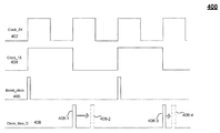
도 4는 부스트 컨버터(300)의 타이밍도를 도시한다. 라인(402)은 부스트 컨버터(300)의 외부 제어기의 클록 신호의 타이밍을 도시한다. 라인(404)은 라인(402)에 도시된 클록 신호로부터 도출된 50% 클록 신호의 타이밍을 도시한다. 라인(406)은 부스트 컨버터(102)에 의한 부스트의 온-스테이지를 시작하도록 플립-플롭(108)을 설정하기 위해 OR 게이트(306)에 의해 플립-플롭(108)에 제공된 부스트 클록 신호의 타이밍을 도시한다. [0057]
4 shows a timing diagram of the
[0058]
라인(408)은 부스트 컨버터(102)에 의한 부스트의 온-스테이지를 종료하도록 플립-플롭(308)을 리셋하기 위해 OR 게이트(306)에 제공된 최대 듀티 사이클 클록 신호의 타이밍을 도시한다. 최대 듀티 사이클 리미트 발생기(310)는, 듀티 사이클을 변경시키기 위해, 도 4에서 화살표에 의해 도시된 바와 같이, 최대 클록 듀티 신호의 타이밍을 조절한다. 최대 듀티 사이클 클록 신호의 펄스는 가변적이다. 펄스들(408-1 및 408-3)은 50% 듀티 사이클에 대응하는 펄스들을 나타낸다. 부스트 컨버터(300)는, 펄스(408-1) 및 펄스(408-3)와는 상이한 시간에 발생하는 최대 듀티 사이클(ClockMaxD) 신호들을 발생시킴으로써 부스트 조절기(302)의 최대 듀티 사이클을 변경시킬 수 있다. 이 예에서, 최대 듀티 사이클(ClockMaxD) 신호는, 펄스(408-1)보더 더 나중의 펄스(408-2), 및 펄스(408-3)보다 더 나중의 펄스(408-4)로서 발생한다. 펄스(408-4)는, 시간 펄스(408-2) 보다 더 짧은 펄스(408-3)가 펄스(408-1) 이후에, 한 번에 발생한다. 도 4에 도시되지 않았지만, 펄스들(408-2 및 408-4)은 각각 펄스(408-1 및 408-3) 이전에 발생할 수 있다. [0058]
[0059]
도 5는 일부 실시예들에 따른 부스트 컨버터(300)의 적응형 듀티 사이클의 타이밍도를 도시한다. 라인(502)은 시간 경과에 따라 부스트 컨버터(300)의 출력 전압(Vout)을 나타낸다. 이 예에서, 라인(502)은 듀티 사이클(D1) 동안 타겟(Vout)에 있다. 듀티 사이클이 듀티 사이클(D2)까지 증가하면, 출력 전압(Vout)은 최대 출력 전압(Vout)을 초과한다. 부스트 컨버터(300)는 부스트 컨버터(300)의 출력 전압을 최대 출력 전압(Vout)까지 제한시키도록 최대 듀티 사이클(Dmax)을 설정한다. [0059]
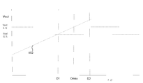
FIG. 5 illustrates a timing diagram of an adaptive duty cycle of
[0060]
도 6은 일부 실시예들에 따른 부스트 컨버터(600)의 블록도를 도시한다. 부스트 컨버터(600)는, 부스트 컨버터(102), 피드백 회로(104), OR 게이트(306), RS 플립-플롭(308), 및 최대 듀티 사이클 리미트 발생기(610)를 포함한다. 부스트 컨버터(600)는, 부스트 컨버터(102) 이외의 컨버터들을 포함할 수 있거나 또는 피드백 회로(104) 이외의 피드백 회로를 포함할 수 있다. 피드백 회로(104)는 OR 게이트(306)의 제 1 입력에 그 트리거 신호를 제공한다. OR 게이트(306)의 제 2 입력은, 최대 듀티 사이클 리미트 발생기(610)로부터 가변적인 최대 듀티 사이클(ClockMaxD) 신호를 수신한다. OR 게이트(306)는, 피드백 회로(104)로부터의 트리거 신호 또는 최대 듀티 사이클(ClockMaxD) 신호가 하이(high)인 것에 대한 응답으로 RS 플립-플롭(308)에 리셋 신호를 제공한다. RS 플립-플롭(308)은 외부 제어기(미도시)로부터의 부스트 클록 입력 또는 OR 게이트(306)로부터의 리셋 신호에 대한 응답으로 부스트 컨버터(102)를 스위칭하기 위한 제어 신호를 제공한다. [0060]
6 shows a block diagram of
[0061]
최대 듀티 사이클 리미트 발생기(610)는 입력 전압(Vin) 및 출력 전압(Vout)에 적응가능하다. 최대 듀티 사이클 리미트 발생기(610)는 입력 전압(Vin) 및 출력 전압(Vout)에 대한 응답으로 출력 전압(Vout)을 제어하기 위해 RS 플립-플롭(308)으로부터 부스트 컨버터(102)로의 제어 신호의 최대 듀티 사이클을 조절한다. 최대 듀티 사이클 리미트 발생기(610)는 최대 듀티 사이클을 증가시키고 이에 의해 입력 전압(Vin)의 감소 또는 출력 전압(Vout)의 감소에 대한 응답으로 부스트 컨버터(102)의 허용 이득을 증가시킨다. 반대로, 최대 듀티 사이클 리미트 발생기(610)는 최대 듀티 사이클을 감소시키고 이에 의해 입력 전압(Vin)의 증가 또는 출력 전압(Vout)의 증가에 대한 응답으로 부스트 컨버터(102)의 허용 이득을 감소시킨다. [0061]
The maximum duty
[0062]
최대 듀티 사이클 리미트 발생기(610)는 전압-전류 컨버터(612), 아날로그 타이머(614) 및 듀티 사이클 리미트 발생기(616)를 포함한다. 전압-전류 컨버터(612)는, 입력 전압(Vin)을, 아날로그 타이머(614)에 제공되는 전류로 컨버팅한다. 전압의 전류로의 컨버전은, 출력 전압의 프로그래밍된 값인 출력 전압 세팅 Vout-set에 기반하거나 또는 그의 함수이다. 아날로그 타이머(614)는, 듀티 사이클의 시작으로부터의 지속기간 동안 부스트 클록과 관련하여 시간을 결정하고, 그 시간을 듀티 사이클 리미트 발생기(314)에 제공한다. 듀티 사이클 리미트 발생기(616)는, 임계 시간과 동일하거나 또는 초과하는 시간에 대한 응답으로 최대 듀티 사이클(ClockMaxD) 신호를 OR 게이트(306)에 제공하고 이에 의해 RS 플립-플롭(308)을 리셋한다. 아래 설명된 바와 같이, 도 8은 듀티 사이클 리미트 발생기(614)의 일 실시예를 도시한다. [0062]
The maximum duty
[0063]
도 7은 일부 실시예들에 따른 듀티 사이클 리미터(700)의 블록도를 도시한다. 듀티 사이클 리미터(700)는 듀티 사이클 리미트 발생기(314)를 위해 사용될 수 있다. 듀티 사이클 리미터(700)는, 버퍼(702), 커패시터(704), 비교기(706), 기준 전압 선택 회로(708), 및 딜레이 회로(710)를 포함한다. 버퍼(702)는, 공급 전압과 접지 사이에 직렬로 커플링된 전류원(714) 및 전류 제한 버퍼(716)를 포함한다. 전류 제한 버퍼(716)는 부스트 컨버터(102)를 스위칭하는 RS 플립-플롭(308)로부터의 제어 신호에 대한 응답으로 비교기(706)를 트리거하기 위해 비교기(706)의 비-반전 입력에 그리고 커패시터(704)를 충전하기 위해 커패시터(704)에 전압 신호를 제공한다. 커패시터(704)의 충전은 타이머로서 기능한다. 커패시터(704)는 방전 회로(미도시)에 의해 다음 듀티 사이클 동안 방전될 수 있다. [0063]
FIG. 7 illustrates a block diagram of a
[0064]
기준 전압 선택 회로(708)는 ADC(312)로부터의 입력 전압 코드(VIN ADC CODE)에 대한 응답으로 비교기(706)의 반전 입력에 기준 전압을 제공한다. 기준 전압은 입력 전압 코드에 의해 표시된 바와 같이 입력 전압(VIN)에 반비례한다. 다시 말해서, 더 높은 입력 전압들이 더 낮은 기준 전압들을 발생시키며, 반대로 더 낮은 입력 전압들이 더 높은 기준 전압들을 발생시킨다. 비교기(706)는 기준 전압 선택 회로(708)에 의해 설정된 기준 전압을 초과하는 커패시터(704) 양단의 전압에 대한 응답으로 RS 플립-플롭(308)을 리셋하기 위한 신호를 딜레이 회로(710)에 제공한다. 전류원(714)으로부터의 전류의 양 및 디폴트 기준 전압 출력은 파워-온 동안 캘리브레이팅되어 임의의 입력 클록 주파수에 대해 작동하도록 그것들을 설정할 수 있다. [0064]
The reference
[0065]
도 8은 일부 실시예들에 따른 듀티 사이클 리미터(800)의 블록도를 도시한다. 듀티 사이클 리미터(800)는 듀티 사이클 리미트 발생기(314)를 위해 사용될 수 있다. 듀티 사이클 리미터(800)는, 버퍼(802), 커패시터(704), 비교기(706), 및 딜레이 회로(710)를 포함한다. 버퍼(802)는, 공급 전압과 접지 사이에 직렬로 커플링된 가변 전류원(814) 및 버퍼(816)를 포함한다. 버퍼(802)는 또한 부스트 컨버터(102)의 출력 전압(Vout)으로부터 도출된 출력 전압 설정(Vout-set)에 대한 응답으로 가변 전류원(814)에 의해 제공되는 전류를 변경시키기 위한 전압-전류 컨버터(818)를 포함한다. 전압-전류 컨버터(818)는, 부스트 컨버터(102) 및 출력 전압 설정(Vout-set)을 스위칭하는 RS 플립-플롭(308)으로부터의 제어 신호에 대한 응답으로 가변 전류원(814)에 의해 제공되는 적응형 전류를 변경시키기 위한 제어 신호를 발생시킨다. 버퍼(816)는 부스트 컨버터(102)를 스위칭하는 RS 플립-플롭(308)로부터의 제어 신호에 대한 응답으로 비교기(706)를 트리거하기 위해 비교기(706)의 비-반전 입력에 그리고 커패시터(704)를 충전하기 위해 커패시터(704)에 전압 신호를 제공한다. [0065]
FIG. 8 illustrates a block diagram of a
[0066]
커패시터(704)의 충전은 타이머로서 기능한다. 커패시터(704)는 방전 회로(미도시)에 의해 다음 듀티 사이클 동안 방전될 수 있다. 고정 기준 전압(Vref)은 비교기(706)의 반전 입력에 제공된다. 듀티 사이클 리미터(800)에서, 비교기(706)에 공급되는 기준 전압(Vref)은 고정되고, 버퍼(802)에 의해 제공되는 전류는 입력 전압(Vin) 및 출력 전압(Vour)에 기반하여 가변적이다. 대조적으로, 듀티 사이클 리미터(800)에서, 비교기(706)에 공급되는 기준 전압(Vref)은 입력 전압(Vin)에 기반하여 가변적이며, 버퍼(702)에 의해 제공되는 전류는 고정된다. 비교기(706)는 기준 전압(Vref)을 초과하는 커패시터(704) 양단의 전압에 대한 응답으로 RS 플립-플롭(308)을 리셋하기 위한 신호를 딜레이 회로(710)에 제공한다. 인식할 바와 같이, 버퍼(802) 및 비교기(706)는 유사한 기능을 제공하는 다른 타입들의 회로들일 수 있다. 최대 듀티 사이클(ClockMaxD) 신호는 부스트 조절기(102)의 더 원활한 제어를 허용하기 위해 적응형이고 연속적이다. [0066]
The charging of the
[0067]
도 9는 일 실시예에 따라 부스트 컨버터(102)의 듀티 사이클을 조절하기 위한 프로세스 흐름(900)을 도시하는 간략화된 도면이다. [0067]
9 is a simplified diagram illustrating a
[0068]
902에서, 부스트 컨버터(102)에 제공될 입력 전압이 수신된다. 904에서, 입력 전압에 대한 응답으로 제어 신호가 발생된다. 제어 신호는, 부스트 컨버터(102)의 출력 전압을 제어하도록 부스트 컨버터(102)의 듀티 사이클을 조절하기 위해 부스트 컨버터(102)에 제공될 것이다. [0068]
At 902, the input voltage to be provided to the
[0069]
904에서 제어 신호를 발생시키는 것은, 906에서, 부스트 컨버터(102)의 입력 전압에 대한 응답으로 디지털화된 신호가 발생되는 것을 포함할 수 있다. 908에서, 부스트 컨버터(102)의 듀티 사이클을 제한하기 위해 최대 듀티 사이클 리미트 신호가 디지털화된 신호에 대한 응답으로 발생된다. [0069]
Generating the control signal at 904 may include generating a digitized signal at 906 in response to the input voltage of the
[0070]
도 10는 일 실시예에 따라 부스트 컨버터(102)의 듀티 사이클을 조절하기 위한 프로세스 흐름(1000)을 도시하는 간략화된 도면이다. [0070]
10 is a simplified diagram illustrating a
[0071]
1002에서, 부스트 컨버터(102)에 제공될 입력 전압이 수신된다. 1004에서, 부스트 컨버터(102)의 입력 전압 및 출력 전압에 대한 응답으로 제어 신호가 발생된다. 제어 신호는, 부스트 컨버터(102)의 출력 전압을 제어하도록 부스트 컨버터(102)의 듀티 사이클을 조절하기 위해 부스트 컨버터(102)에 제공될 것이다. [0071]
At 1002, the input voltage to be provided to the
[0072] 1004에서 제어 신호를 발생시키는 것은, 1006에서, 부스트 컨버터의 입력 전압 및 출력 전압에 대한 응답으로 전류가 발생되는 것을 포함할 수 있다. 1008에서, 발생된 전류는 타이밍된다. 1010에서, 최대 듀티 사이클 리미트 신호는 타이밍된 전류에 대한 응답으로 발생된다. [0072] Generating a control signal at 1004 may include generating a current at 1006 in response to the input voltage and the output voltage of the boost converter. At 1008, the generated current is timed. At 1010, the maximum duty cycle limit signal is generated in response to the timed current.
[0073] 전술한 설명은, 특정 실시예들의 양상들이 구현될 수 있는 방법의 예시들과 함께 본 개시내용의 다양한 실시예들을 도시한다. 전술한 예시들은, 유일한 실시예들인 것으로 간주되어서는 안되며, 이하의 청구범위들에 의해 정의되는 것과 같이 특정 실시예들의 유연성 및 이점들을 예시하기 위해 제공된다. 전술한 개시내용 및 이하의 청구항들에 기초하여, 청구항들에 의해 정의된 바와 같은 본 개시내용의 범위를 벗어나지 않고 다른 배열들, 실시예들, 구현들, 및 등가물들이 사용될 수 있다. [0073] The foregoing description, together with illustrative examples of how aspects of the specific embodiments may be implemented, illustrates various embodiments of the present disclosure. The foregoing examples are provided to illustrate the flexibility and advantages of particular embodiments, as defined by the following claims, not to be considered as unique embodiments. Other arrangements, embodiments, implementations, and equivalents may be used without departing from the scope of the present disclosure as defined by the claims, based on the foregoing disclosure and the following claims.
Claims (20)
상기 부스트 컨버터에 제공되는 입력 전압을 수신하고, 상기 입력 전압에 대한 응답으로 상기 부스트 컨버터의 출력 전압을 제어하도록 상기 부스트 컨버터의 상기 듀티 사이클을 조절하기 위해 상기 부스트 컨버터에 제공될 제어 신호를 발생시키도록 구성되는 듀티 사이클 리미터 발생기(duty cycle limiter generator)를 포함하는,
부스트 컨버터의 듀티 사이클을 조절하기 위한 제어 회로. A control circuit for adjusting a duty cycle of a boost converter,
A boost converter configured to receive an input voltage provided to the boost converter and generate a control signal to be provided to the boost converter to adjust the duty cycle of the boost converter to control the output voltage of the boost converter in response to the input voltage And a duty cycle limiter generator configured to < RTI ID = 0.0 >
A control circuit for regulating the duty cycle of the boost converter.
상기 듀티 사이클 리미터 발생기는:
상기 부스트 컨버터의 입력 전압에 대한 응답으로 디지털화된 신호를 발생시키기 위한 아날로그-디지털 컨버터; 및
상기 아날로그-디지털 컨버터에 의해 발생되는 상기 디지털화된 신호에 대한 응답으로 상기 부스트 컨버터의 상기 듀티 사이클을 제한하기 위해 최대 듀티 사이클 신호를 발생시키기 위한 최대 듀티 사이클 리미트 발생기를 포함하는,
부스트 컨버터의 듀티 사이클을 조절하기 위한 제어 회로. The method according to claim 1,
The duty cycle limiter generator comprising:
An analog-to-digital converter for generating a digitized signal in response to an input voltage of the boost converter; And
And a maximum duty cycle limit generator for generating a maximum duty cycle signal to limit said duty cycle of said boost converter in response to said digitized signal generated by said analog to digital converter.
A control circuit for regulating the duty cycle of the boost converter.
상기 최대 듀티 사이클 리미트 발생기는:
상기 부스트 컨버터를 제어하도록 제공된 스위칭 신호에 대한 응답으로 전류를 제공하기 위한 전류 제한 버퍼(current starved buffer);
상기 전류 제한 버퍼의 출력과 접지 사이에 커플링된 커패시터;
상기 디지털화된 신호에 대한 응답으로 기준 전압을 발생시키기 위한 기준 전압 선택 회로; 및
상기 커패시터 양단의 전압 및 상기 기준 전압에 대한 응답으로 최대 듀티 사이클 신호를 발생시키기 위한 비교기를 포함하는,
부스트 컨버터의 듀티 사이클을 조절하기 위한 제어 회로. 3. The method of claim 2,
The maximum duty cycle limit generator comprises:
A current starved buffer for providing current in response to a switching signal provided to control the boost converter;
A capacitor coupled between the output of the current limit buffer and ground;
A reference voltage selection circuit for generating a reference voltage in response to the digitized signal; And
A comparator for generating a maximum duty cycle signal in response to the voltage across the capacitor and the reference voltage,
A control circuit for regulating the duty cycle of the boost converter.
상기 최대 듀티 사이클 리미트 발생기는 상기 부스트 컨버터의 출력 전압에 대한 응답으로 상기 최대 듀티 사이클 신호를 추가로 발생시키는,
부스트 컨버터의 듀티 사이클을 조절하기 위한 제어 회로. The method according to claim 1,
Wherein the maximum duty cycle limit generator further generates the maximum duty cycle signal in response to an output voltage of the boost converter,
A control circuit for regulating the duty cycle of the boost converter.
상기 최대 듀티 사이클 리미트 발생기는:
상기 부스트 컨버터의 상기 입력 전압 및 출력 전압에 대한 응답으로 전류를 발생시키기 위한 전압-전류 컨버터;
상기 전류를 타이밍하기 위한 아날로그 타이머; 및
타이밍된 전류에 대한 응답으로 최대 듀티 사이클 신호를 발생시키기 위한 듀티 사이클 리미트 발생기를 포함하는,
부스트 컨버터의 듀티 사이클을 조절하기 위한 제어 회로. The method according to claim 1,
The maximum duty cycle limit generator comprises:
A voltage-to-current converter for generating a current in response to the input voltage and the output voltage of the boost converter;
An analog timer for timing said current; And
And a duty cycle limit generator for generating a maximum duty cycle signal in response to the timed current.
A control circuit for regulating the duty cycle of the boost converter.
상기 아날로그 타이머는 상기 전류를 저장하기 위해 상기 전압-전류 컨버터의 출력에 커플링된 커패시터인,
부스트 컨버터의 듀티 사이클을 조절하기 위한 제어 회로. 6. The method of claim 5,
Wherein the analog timer is a capacitor coupled to the output of the voltage-to-current converter for storing the current,
A control circuit for regulating the duty cycle of the boost converter.
상기 최대 듀티 사이클 리미트 발생기는:
상기 전압-전류 컨버터로부터의 전류에 대한 응답으로 바이어스 전류를 발생시키기 위한 가변 전류원;
상기 부스트 컨버터를 제어하도록 제공된 스위칭 신호 및 상기 바이어스 전류에 대한 응답으로 버퍼 전류를 제공하기 위한 버퍼;
상기 전류 제한 버퍼의 출력과 접지 사이에 커플링된 커패시터; 및
상기 커패시터 양단의 전압 및 기준 전압에 대한 응답으로 최대 듀티 사이클 신호를 발생시키기 위한 비교기를 포함하는,
부스트 컨버터의 듀티 사이클을 조절하기 위한 제어 회로. 6. The method of claim 5,
The maximum duty cycle limit generator comprises:
A variable current source for generating a bias current in response to a current from the voltage-current converter;
A buffer for providing a buffer current in response to the bias current and a switching signal provided to control the boost converter;
A capacitor coupled between the output of the current limit buffer and ground; And
A comparator for generating a maximum duty cycle signal in response to a voltage across the capacitor and a reference voltage,
A control circuit for regulating the duty cycle of the boost converter.
상기 부스트 컨버터에 제공되는 입력 전압을 수신하는 단계; 및
상기 입력 전압에 대한 응답으로 상기 부스트 컨버터의 출력 전압을 제어하도록 상기 부스트 컨버터의 상기 듀티 사이클을 조절하기 위해 상기 부스트 컨버터에 제공하기 위한 제어 신호를 발생시키는 단계를 포함하는,
부스트 컨버터의 듀티 사이클을 조절하기 위한 방법. CLAIMS 1. A method for adjusting a duty cycle of a boost converter,
Receiving an input voltage provided to the boost converter; And
And generating a control signal for providing to the boost converter to adjust the duty cycle of the boost converter to control the output voltage of the boost converter in response to the input voltage.
A method for adjusting a duty cycle of a boost converter.
상기 제어 신호를 발생시키는 단계는:
상기 부스트 컨버터의 상기 입력 전압에 대한 응답으로 디지털화된 신호를 발생시키는 단계; 및
상기 디지털화된 신호에 대한 응답으로 상기 부스트 컨버터의 상기 듀티 사이클을 제한하기 위해 최대 듀티 사이클 신호를 발생시키는 단계를 포함하는,
부스트 컨버터의 듀티 사이클을 조절하기 위한 방법. 9. The method of claim 8,
Wherein generating the control signal comprises:
Generating a digitized signal in response to the input voltage of the boost converter; And
Generating a maximum duty cycle signal to limit the duty cycle of the boost converter in response to the digitized signal.
A method for adjusting a duty cycle of a boost converter.
상기 최대 듀티 사이클 신호를 발생시키는 단계는:
상기 부스트 컨버터를 제어하도록 제공된 스위칭 신호에 대한 응답으로 전류를 발생시키는 단계;
상기 전류를 저장하는 단계;
상기 디지털화된 신호에 대한 응답으로 기준 전압을 발생시키는 단계; 및
최대 듀티 사이클 신호를 발생시키기 위해, 저장된 버퍼 전류와 상기 기준 전압을 비교하는 단계를 포함하는,
부스트 컨버터의 듀티 사이클을 조절하기 위한 방법. 10. The method of claim 9,
Wherein generating the maximum duty cycle signal comprises:
Generating a current in response to a switching signal provided to control the boost converter;
Storing the current;
Generating a reference voltage in response to the digitized signal; And
And comparing the stored buffer current to the reference voltage to generate a maximum duty cycle signal.
A method for adjusting a duty cycle of a boost converter.
상기 제어 신호를 발생시키는 단계는, 상기 부스트 컨버터의 상기 입력 전압 및 출력 전압에 대한 응답으로 제어 신호를 발생시키는 단계를 더 포함하는,
부스트 컨버터의 듀티 사이클을 조절하기 위한 방법. 9. The method of claim 8,
Wherein generating the control signal further comprises generating a control signal in response to the input voltage and the output voltage of the boost converter.
A method for adjusting a duty cycle of a boost converter.
상기 제어 신호를 발생시키는 단계는:
상기 부스트 컨버터의 상기 입력 전압 및 출력 전압에 대한 응답으로 전류를 발생시키는 단계;
발생된 전류를 타이밍하는 단계; 및
타이밍된 전류에 대한 응답으로 최대 듀티 사이클 신호를 발생시키는 단계를 포함하는,
부스트 컨버터의 듀티 사이클을 조절하기 위한 방법. 9. The method of claim 8,
Wherein generating the control signal comprises:
Generating a current in response to the input voltage and the output voltage of the boost converter;
Timing the generated current; And
And generating a maximum duty cycle signal in response to the timed current.
A method for adjusting a duty cycle of a boost converter.
상기 발생된 전류를 타이밍하는 단계는, 상기 발생된 전류의 전하를 저장하는 단계를 포함하는,
부스트 컨버터의 듀티 사이클을 조절하기 위한 방법. 13. The method of claim 12,
Wherein the step of timing the generated current comprises the step of storing the charge of the generated current.
A method for adjusting a duty cycle of a boost converter.
상기 최대 듀티 사이클 신호를 발생시키는 단계는:
상기 발생된 전류에 대한 응답으로 바이어스 전류를 발생시키는 단계;
상기 부스트 컨버터를 제어하도록 제공된 스위칭 신호 및 상기 바이어스 전류에 대한 응답으로 버퍼 전류를 발생시키는 단계;
상기 버퍼 전류를 저장하는 단계; 및
저장된 버퍼 전류를 나타내는 전압 및 기준 전압에 대한 응답으로 최대 듀티 사이클 신호를 발생시키기 위해 상기 저장된 버퍼 전류와 기준 전압을 비교하는 단계를 포함하는,
부스트 컨버터의 듀티 사이클을 조절하기 위한 방법. 13. The method of claim 12,
Wherein generating the maximum duty cycle signal comprises:
Generating a bias current in response to the generated current;
Generating a buffer current in response to the bias current and a switching signal provided to control the boost converter;
Storing the buffer current; And
Comparing the stored buffer current with a reference voltage to generate a maximum duty cycle signal in response to a voltage representing the stored buffer current and a reference voltage,
A method for adjusting a duty cycle of a boost converter.
상기 부스트 컨버터에 제공되는 입력 전압을 수신하기 위한 수단; 및
상기 입력 전압에 대한 응답으로 상기 부스트 컨버터의 출력 전압을 제어하도록 상기 부스트 컨버터의 상기 듀티 사이클을 조절하기 위해 상기 부스트 컨버터에 제공하기 위한 제어 신호를 발생시키기 위한 수단을 포함하는,
부스트 컨버터의 듀티 사이클을 조절하기 위한 제어 회로. A control circuit for adjusting a duty cycle of a boost converter,
Means for receiving an input voltage provided to the boost converter; And
And means for generating a control signal for providing to the boost converter to adjust the duty cycle of the boost converter to control the output voltage of the boost converter in response to the input voltage.
A control circuit for regulating the duty cycle of the boost converter.
상기 제어 신호를 발생시키기 위한 수단은:
상기 부스트 컨버터의 상기 입력 전압에 대한 응답으로 디지털화된 신호를 발생시키기 위한 수단; 및
상기 디지털화된 신호에 대한 응답으로 상기 부스트 컨버터의 상기 듀티 사이클을 제한하기 위해 최대 듀티 사이클 신호를 발생시키기 위한 수단을 포함하는,
부스트 컨버터의 듀티 사이클을 조절하기 위한 제어 회로. 16. The method of claim 15,
Wherein the means for generating the control signal comprises:
Means for generating a digitized signal in response to the input voltage of the boost converter; And
And means for generating a maximum duty cycle signal to limit the duty cycle of the boost converter in response to the digitized signal.
A control circuit for regulating the duty cycle of the boost converter.
상기 최대 듀티 사이클 신호를 발생시키기 위한 수단은:
상기 부스트 컨버터를 제어하도록 제공된 스위칭 신호에 대한 응답으로 전류를 발생시키기 위한 수단;
상기 전류를 저장하기 위한 수단;
상기 디지털화된 신호에 대한 응답으로 기준 전압을 발생시키기 위한 수단; 및
최대 듀티 사이클 신호를 발생시키기 위해, 저장된 버퍼 전류와 상기 기준 전압을 비교하기 위한 수단을 포함하는,
부스트 컨버터의 듀티 사이클을 조절하기 위한 제어 회로. 17. The method of claim 16,
Wherein the means for generating the maximum duty cycle signal comprises:
Means for generating a current in response to a switching signal provided to control the boost converter;
Means for storing the current;
Means for generating a reference voltage in response to the digitized signal; And
Means for comparing the stored buffer current and the reference voltage to generate a maximum duty cycle signal,
A control circuit for regulating the duty cycle of the boost converter.
상기 제어 신호를 발생시키기 위한 수단은, 상기 부스트 컨버터의 상기 입력 전압 및 출력 전압에 대한 응답으로 상기 제어 신호를 발생시키기 위한 수단을 더 포함하는,
부스트 컨버터의 듀티 사이클을 조절하기 위한 제어 회로. 16. The method of claim 15,
Wherein the means for generating the control signal further comprises means for generating the control signal in response to the input voltage and the output voltage of the boost converter.
A control circuit for regulating the duty cycle of the boost converter.
상기 제어 신호를 발생시키기 위한 수단은:
상기 부스트 컨버터의 상기 입력 전압 및 출력 전압에 대한 응답으로 전류를 발생시키기 위한 수단;
발생된 전류를 타이밍하기 위한 수단; 및
타이밍된 전류에 대한 응답으로 최대 듀티 사이클 신호를 발생시키기 위한 수단을 포함하는,
부스트 컨버터의 듀티 사이클을 조절하기 위한 제어 회로. 16. The method of claim 15,
Wherein the means for generating the control signal comprises:
Means for generating a current in response to the input voltage and the output voltage of the boost converter;
Means for timing the generated current; And
And means for generating a maximum duty cycle signal in response to the timed current.
A control circuit for regulating the duty cycle of the boost converter.
상기 발생된 전류를 타이밍하기 위한 수단은, 발생된 전류의 전하를 저장하기 위한 수단을 포함하는,
부스트 컨버터의 듀티 사이클을 조절하기 위한 제어 회로. 20. The method of claim 19,
Wherein the means for timing the generated current comprises means for storing the charge of the generated current,
A control circuit for regulating the duty cycle of the boost converter.
Applications Claiming Priority (3)
| Application Number | Priority Date | Filing Date | Title |
|---|---|---|---|
| US14/534,034 US10374514B2 (en) | 2014-11-05 | 2014-11-05 | Boost converters having self-adaptive maximum duty-cycle-limit control |
| US14/534,034 | 2014-11-05 | ||
| PCT/US2015/053706 WO2016073090A1 (en) | 2014-11-05 | 2015-10-02 | Boost converters having self-adaptive maximum duty-cycle-limit control |
Publications (1)
| Publication Number | Publication Date |
|---|---|
| KR20170078647A true KR20170078647A (en) | 2017-07-07 |
Family
ID=54330061
Family Applications (1)
| Application Number | Title | Priority Date | Filing Date |
|---|---|---|---|
| KR1020177011518A KR20170078647A (en) | 2014-11-05 | 2015-10-02 | Boost converters having self-adaptive maximum duty-cycle-limit control |
Country Status (6)
| Country | Link |
|---|---|
| US (1) | US10374514B2 (en) |
| EP (1) | EP3216118A1 (en) |
| JP (1) | JP2017534243A (en) |
| KR (1) | KR20170078647A (en) |
| CN (1) | CN107078637A (en) |
| WO (1) | WO2016073090A1 (en) |
Cited By (1)
| Publication number | Priority date | Publication date | Assignee | Title |
|---|---|---|---|---|
| US11290014B2 (en) | 2019-08-02 | 2022-03-29 | Electronics And Telecommunications Research Institute | Boost DC-DC converter using DSM, duty controller for boost DC-DC converter, and method for configuring duty controller |
Families Citing this family (6)
| Publication number | Priority date | Publication date | Assignee | Title |
|---|---|---|---|---|
| US10270338B2 (en) * | 2017-09-19 | 2019-04-23 | Texas Instruments Incorporated | Shunt regulator including ramp control circuit |
| CN108616209B (en) * | 2018-04-17 | 2019-10-18 | 华南理工大学 | A kind of dynamic regulating method of digital power largest duty cycle value |
| CN109906556B (en) * | 2019-01-22 | 2022-10-04 | 香港应用科技研究院有限公司 | Duty cycle controller with calibration circuit |
| CN111817562B (en) * | 2020-07-08 | 2021-06-22 | 无锡力芯微电子股份有限公司 | Buck type DC-DC converter |
| CN112098708B (en) * | 2020-11-23 | 2021-02-02 | 成都市易冲半导体有限公司 | Line voltage information detection circuit and detection method for secondary side PD controller |
| CN113258760B (en) * | 2021-05-14 | 2022-11-11 | 珠海格力电器股份有限公司 | Circuit control method and device, electronic equipment and storage medium |
Family Cites Families (13)
| Publication number | Priority date | Publication date | Assignee | Title |
|---|---|---|---|---|
| US6977492B2 (en) | 2002-07-10 | 2005-12-20 | Marvell World Trade Ltd. | Output regulator |
| US6922346B2 (en) | 2003-07-23 | 2005-07-26 | Texas Instruments Incorporated | System and method to limit maximum duty cycle and/or provide a maximum volt-second clamp |
| US6992469B1 (en) | 2004-12-08 | 2006-01-31 | Kiawe Forest, Llc | Digital voltage regulator for DC/DC converters |
| US8059432B2 (en) | 2007-12-12 | 2011-11-15 | Semiconductor Components Industries, Llc. | PWM controller having drive control with input voltage sensing and method therefor |
| JP4577420B2 (en) * | 2008-07-10 | 2010-11-10 | 富士ゼロックス株式会社 | Image processing apparatus and image processing program |
| JP5399734B2 (en) | 2008-09-30 | 2014-01-29 | スパンション エルエルシー | OUTPUT VOLTAGE CONTROL DEVICE, OUTPUT VOLTAGE CONTROL METHOD, AND ELECTRONIC DEVICE |
| TWI371906B (en) | 2009-03-09 | 2012-09-01 | Delta Electronics Inc | Two-stage switching power conversion circuit |
| US8232787B2 (en) | 2009-04-28 | 2012-07-31 | Analog Devices, Inc. | Pulse time detector, a controller for a switched mode power supply, and a switched mode power supply including such a controller |
| US20110140684A1 (en) | 2009-12-10 | 2011-06-16 | Chiccony Power Technology Co., Ltd. | Power controller having externally adjustable duty cycle |
| CN102598866B (en) * | 2010-06-04 | 2014-08-20 | 丰裕国际电子私人有限公司 | Device and method for driving LEDs |
| US8564259B2 (en) * | 2010-11-02 | 2013-10-22 | Intersil Americas LLC | Clock phase shifter for use with buck-boost converter |
| US8970068B2 (en) | 2011-02-10 | 2015-03-03 | Draker, Inc. | Pseudo-random bit sequence generation for maximum power point tracking in photovoltaic arrays |
| US8564267B2 (en) * | 2011-08-26 | 2013-10-22 | Maxim Integrated Products, Inc. | Multi-mode parameter analyzer for power supplies |
-
2014
- 2014-11-05 US US14/534,034 patent/US10374514B2/en not_active Expired - Fee Related
-
2015
- 2015-10-02 KR KR1020177011518A patent/KR20170078647A/en unknown
- 2015-10-02 CN CN201580059849.9A patent/CN107078637A/en active Pending
- 2015-10-02 EP EP15781520.0A patent/EP3216118A1/en not_active Withdrawn
- 2015-10-02 JP JP2017543711A patent/JP2017534243A/en active Pending
- 2015-10-02 WO PCT/US2015/053706 patent/WO2016073090A1/en active Application Filing
Cited By (1)
| Publication number | Priority date | Publication date | Assignee | Title |
|---|---|---|---|---|
| US11290014B2 (en) | 2019-08-02 | 2022-03-29 | Electronics And Telecommunications Research Institute | Boost DC-DC converter using DSM, duty controller for boost DC-DC converter, and method for configuring duty controller |
Also Published As
| Publication number | Publication date |
|---|---|
| EP3216118A1 (en) | 2017-09-13 |
| US10374514B2 (en) | 2019-08-06 |
| WO2016073090A1 (en) | 2016-05-12 |
| CN107078637A (en) | 2017-08-18 |
| US20160126839A1 (en) | 2016-05-05 |
| JP2017534243A (en) | 2017-11-16 |
Similar Documents
| Publication | Publication Date | Title |
|---|---|---|
| KR20170078647A (en) | Boost converters having self-adaptive maximum duty-cycle-limit control | |
| US10333403B2 (en) | Adaptive on-time switching converter | |
| US9529373B2 (en) | Switching regulator and control circuit and control method therefor | |
| US11342856B2 (en) | Power converter controller with stability compensation | |
| US10250122B2 (en) | Multi-phase control for pulse width modulation power converters | |
| US9742302B2 (en) | Zero-crossing detection circuit and switching power supply thereof | |
| US10566901B2 (en) | Constant-frequency control method with fast transient | |
| US9614437B2 (en) | Switching regulator and control circuit and control method therefor | |
| CN105262329A (en) | Constant on-time controlled switching converter and controller and control method thereof | |
| US10381927B2 (en) | Pulse-frequency modulation constant on-time with peak-current servo | |
| US9160229B2 (en) | DC-DC converter | |
| US20170187213A1 (en) | Battery charging circuit with high capacity, control circuit and associated control method | |
| US10033273B1 (en) | System and method for controlling switching power supply | |
| US10348111B2 (en) | Charging circuit and the method thereof | |
| US20190222122A1 (en) | Control and Detection of Average Phase Current in Switching DC-DC Power Converters | |
| US10103720B2 (en) | Method and apparatus for a buck converter with pulse width modulation and pulse frequency modulation mode | |
| US6930526B1 (en) | Quasi-feedforward PWM modulator | |
| US9847720B2 (en) | SIDO power converter operable in discontinuous conduction mode and control method thereof | |
| CN109921627B (en) | Apparatus and method for limiting electromagnetic interference in a switching converter | |
| CN107317462B (en) | Switch mode power supply control | |
| US10060954B2 (en) | Load capacitance determination circuitry and power supply control | |
| US10720839B1 (en) | System and method for operating a switching converter in light load | |
| US9081403B1 (en) | Optimal compensating ramp generator for fixed frequency current mode DC-DC converters | |
| US20220360170A1 (en) | Power delivery control circuit | |
| US9653993B2 (en) | Signal control circuit and switching apparatus for increased current control |