JP2017534083A - Method for producing a soft electro-optic cell - Google Patents
Method for producing a soft electro-optic cell Download PDFInfo
- Publication number
- JP2017534083A JP2017534083A JP2017526079A JP2017526079A JP2017534083A JP 2017534083 A JP2017534083 A JP 2017534083A JP 2017526079 A JP2017526079 A JP 2017526079A JP 2017526079 A JP2017526079 A JP 2017526079A JP 2017534083 A JP2017534083 A JP 2017534083A
- Authority
- JP
- Japan
- Prior art keywords
- substrate
- electro
- boundary
- optic material
- liquid crystal
- Prior art date
- Legal status (The legal status is an assumption and is not a legal conclusion. Google has not performed a legal analysis and makes no representation as to the accuracy of the status listed.)
- Granted
Links
- 238000004519 manufacturing process Methods 0.000 title claims abstract description 28
- 239000000758 substrate Substances 0.000 claims abstract description 210
- 238000000034 method Methods 0.000 claims abstract description 129
- 125000006850 spacer group Chemical group 0.000 claims abstract description 68
- 239000000382 optic material Substances 0.000 claims abstract description 49
- 239000000463 material Substances 0.000 claims abstract description 48
- 238000000151 deposition Methods 0.000 claims abstract description 16
- 238000011049 filling Methods 0.000 claims abstract description 10
- 239000004973 liquid crystal related substance Substances 0.000 claims description 103
- 239000000565 sealant Substances 0.000 claims description 75
- 230000008569 process Effects 0.000 claims description 46
- 239000004033 plastic Substances 0.000 claims description 33
- 229920003023 plastic Polymers 0.000 claims description 33
- 239000000203 mixture Substances 0.000 claims description 31
- 230000003287 optical effect Effects 0.000 claims description 20
- 239000007788 liquid Substances 0.000 claims description 10
- 238000005520 cutting process Methods 0.000 claims description 7
- 238000007639 printing Methods 0.000 claims description 6
- 238000005192 partition Methods 0.000 claims description 2
- 229920002457 flexible plastic Polymers 0.000 abstract description 4
- 210000004027 cell Anatomy 0.000 description 89
- 239000010410 layer Substances 0.000 description 40
- 239000000975 dye Substances 0.000 description 24
- 229920000642 polymer Polymers 0.000 description 20
- 238000000576 coating method Methods 0.000 description 14
- 239000011521 glass Substances 0.000 description 14
- 239000004642 Polyimide Substances 0.000 description 9
- 229920001721 polyimide Polymers 0.000 description 9
- 239000011248 coating agent Substances 0.000 description 8
- 239000000126 substance Substances 0.000 description 8
- 239000002775 capsule Substances 0.000 description 7
- 230000008021 deposition Effects 0.000 description 7
- 238000005429 filling process Methods 0.000 description 7
- 230000003993 interaction Effects 0.000 description 7
- 238000010030 laminating Methods 0.000 description 7
- 238000003825 pressing Methods 0.000 description 7
- 239000004983 Polymer Dispersed Liquid Crystal Substances 0.000 description 6
- 239000000853 adhesive Substances 0.000 description 6
- 230000001070 adhesive effect Effects 0.000 description 6
- 230000005540 biological transmission Effects 0.000 description 6
- 238000010586 diagram Methods 0.000 description 5
- 230000005684 electric field Effects 0.000 description 5
- 238000005538 encapsulation Methods 0.000 description 5
- 239000010408 film Substances 0.000 description 5
- 238000003475 lamination Methods 0.000 description 5
- 239000004593 Epoxy Substances 0.000 description 4
- 230000008901 benefit Effects 0.000 description 4
- 238000005191 phase separation Methods 0.000 description 4
- 238000010521 absorption reaction Methods 0.000 description 3
- 230000004888 barrier function Effects 0.000 description 3
- 239000008393 encapsulating agent Substances 0.000 description 3
- 238000003698 laser cutting Methods 0.000 description 3
- 239000012528 membrane Substances 0.000 description 3
- 239000002985 plastic film Substances 0.000 description 3
- 230000010287 polarization Effects 0.000 description 3
- 229920000139 polyethylene terephthalate Polymers 0.000 description 3
- 239000005020 polyethylene terephthalate Substances 0.000 description 3
- 238000006116 polymerization reaction Methods 0.000 description 3
- 230000001681 protective effect Effects 0.000 description 3
- 239000007787 solid Substances 0.000 description 3
- 239000007921 spray Substances 0.000 description 3
- XLYOFNOQVPJJNP-UHFFFAOYSA-N water Chemical compound O XLYOFNOQVPJJNP-UHFFFAOYSA-N 0.000 description 3
- 238000003466 welding Methods 0.000 description 3
- 239000004696 Poly ether ether ketone Substances 0.000 description 2
- 239000004697 Polyetherimide Substances 0.000 description 2
- 230000015572 biosynthetic process Effects 0.000 description 2
- 230000008859 change Effects 0.000 description 2
- 238000001723 curing Methods 0.000 description 2
- 230000007547 defect Effects 0.000 description 2
- 229920001971 elastomer Polymers 0.000 description 2
- 239000012530 fluid Substances 0.000 description 2
- 239000011888 foil Substances 0.000 description 2
- AMGQUBHHOARCQH-UHFFFAOYSA-N indium;oxotin Chemical compound [In].[Sn]=O AMGQUBHHOARCQH-UHFFFAOYSA-N 0.000 description 2
- 238000007641 inkjet printing Methods 0.000 description 2
- 229910052751 metal Inorganic materials 0.000 description 2
- 239000002184 metal Substances 0.000 description 2
- DVDUMIQZEUTAGK-UHFFFAOYSA-N p-nitrophenyl butyrate Chemical compound CCCC(=O)OC1=CC=C([N+]([O-])=O)C=C1 DVDUMIQZEUTAGK-UHFFFAOYSA-N 0.000 description 2
- 229920001230 polyarylate Polymers 0.000 description 2
- 239000004417 polycarbonate Substances 0.000 description 2
- 229920000515 polycarbonate Polymers 0.000 description 2
- 229920002530 polyetherether ketone Polymers 0.000 description 2
- 229920001601 polyetherimide Polymers 0.000 description 2
- -1 polyethylene terephthalate Polymers 0.000 description 2
- 230000005855 radiation Effects 0.000 description 2
- 239000011347 resin Substances 0.000 description 2
- 229920005989 resin Polymers 0.000 description 2
- 238000005096 rolling process Methods 0.000 description 2
- 239000005060 rubber Substances 0.000 description 2
- 238000006748 scratching Methods 0.000 description 2
- 230000002393 scratching effect Effects 0.000 description 2
- 238000007650 screen-printing Methods 0.000 description 2
- NIXOWILDQLNWCW-UHFFFAOYSA-M Acrylate Chemical compound [O-]C(=O)C=C NIXOWILDQLNWCW-UHFFFAOYSA-M 0.000 description 1
- 229920002284 Cellulose triacetate Polymers 0.000 description 1
- 239000004986 Cholesteric liquid crystals (ChLC) Substances 0.000 description 1
- PEDCQBHIVMGVHV-UHFFFAOYSA-N Glycerine Chemical compound OCC(O)CO PEDCQBHIVMGVHV-UHFFFAOYSA-N 0.000 description 1
- 239000004839 Moisture curing adhesive Substances 0.000 description 1
- 229920012266 Poly(ether sulfone) PES Polymers 0.000 description 1
- 239000004952 Polyamide Substances 0.000 description 1
- 229920002367 Polyisobutene Polymers 0.000 description 1
- 239000004820 Pressure-sensitive adhesive Substances 0.000 description 1
- 238000003848 UV Light-Curing Methods 0.000 description 1
- NNLVGZFZQQXQNW-ADJNRHBOSA-N [(2r,3r,4s,5r,6s)-4,5-diacetyloxy-3-[(2s,3r,4s,5r,6r)-3,4,5-triacetyloxy-6-(acetyloxymethyl)oxan-2-yl]oxy-6-[(2r,3r,4s,5r,6s)-4,5,6-triacetyloxy-2-(acetyloxymethyl)oxan-3-yl]oxyoxan-2-yl]methyl acetate Chemical compound O([C@@H]1O[C@@H]([C@H]([C@H](OC(C)=O)[C@H]1OC(C)=O)O[C@H]1[C@@H]([C@@H](OC(C)=O)[C@H](OC(C)=O)[C@@H](COC(C)=O)O1)OC(C)=O)COC(=O)C)[C@@H]1[C@@H](COC(C)=O)O[C@@H](OC(C)=O)[C@H](OC(C)=O)[C@H]1OC(C)=O NNLVGZFZQQXQNW-ADJNRHBOSA-N 0.000 description 1
- 230000002730 additional effect Effects 0.000 description 1
- 239000000654 additive Substances 0.000 description 1
- 239000012790 adhesive layer Substances 0.000 description 1
- 230000004075 alteration Effects 0.000 description 1
- 238000000149 argon plasma sintering Methods 0.000 description 1
- 230000005779 cell damage Effects 0.000 description 1
- 208000037887 cell injury Diseases 0.000 description 1
- 230000003098 cholesteric effect Effects 0.000 description 1
- 229920001940 conductive polymer Polymers 0.000 description 1
- 239000004020 conductor Substances 0.000 description 1
- 238000010924 continuous production Methods 0.000 description 1
- 229920001577 copolymer Polymers 0.000 description 1
- 210000002858 crystal cell Anatomy 0.000 description 1
- 230000006378 damage Effects 0.000 description 1
- 230000001419 dependent effect Effects 0.000 description 1
- 238000011161 development Methods 0.000 description 1
- 230000018109 developmental process Effects 0.000 description 1
- 238000002845 discoloration Methods 0.000 description 1
- 238000009826 distribution Methods 0.000 description 1
- 238000001035 drying Methods 0.000 description 1
- 230000000694 effects Effects 0.000 description 1
- 238000005516 engineering process Methods 0.000 description 1
- 238000001704 evaporation Methods 0.000 description 1
- 239000004744 fabric Substances 0.000 description 1
- 238000013007 heat curing Methods 0.000 description 1
- 238000010438 heat treatment Methods 0.000 description 1
- 238000007731 hot pressing Methods 0.000 description 1
- 230000031700 light absorption Effects 0.000 description 1
- 230000013011 mating Effects 0.000 description 1
- 238000002156 mixing Methods 0.000 description 1
- 239000002070 nanowire Substances 0.000 description 1
- 239000002245 particle Substances 0.000 description 1
- 238000000059 patterning Methods 0.000 description 1
- 239000008188 pellet Substances 0.000 description 1
- 230000035699 permeability Effects 0.000 description 1
- 238000000206 photolithography Methods 0.000 description 1
- 229920002647 polyamide Polymers 0.000 description 1
- 239000011112 polyethylene naphthalate Substances 0.000 description 1
- 238000009877 rendering Methods 0.000 description 1
- 230000004044 response Effects 0.000 description 1
- 238000007761 roller coating Methods 0.000 description 1
- 238000007790 scraping Methods 0.000 description 1
- 239000002094 self assembled monolayer Substances 0.000 description 1
- 239000013545 self-assembled monolayer Substances 0.000 description 1
- 238000000926 separation method Methods 0.000 description 1
- 230000001568 sexual effect Effects 0.000 description 1
- 238000004381 surface treatment Methods 0.000 description 1
- 229920001187 thermosetting polymer Polymers 0.000 description 1
- 230000009974 thixotropic effect Effects 0.000 description 1
- 239000002699 waste material Substances 0.000 description 1
- 238000009736 wetting Methods 0.000 description 1
Images


Classifications
-
- G—PHYSICS
- G02—OPTICS
- G02F—OPTICAL DEVICES OR ARRANGEMENTS FOR THE CONTROL OF LIGHT BY MODIFICATION OF THE OPTICAL PROPERTIES OF THE MEDIA OF THE ELEMENTS INVOLVED THEREIN; NON-LINEAR OPTICS; FREQUENCY-CHANGING OF LIGHT; OPTICAL LOGIC ELEMENTS; OPTICAL ANALOGUE/DIGITAL CONVERTERS
- G02F1/00—Devices or arrangements for the control of the intensity, colour, phase, polarisation or direction of light arriving from an independent light source, e.g. switching, gating or modulating; Non-linear optics
- G02F1/01—Devices or arrangements for the control of the intensity, colour, phase, polarisation or direction of light arriving from an independent light source, e.g. switching, gating or modulating; Non-linear optics for the control of the intensity, phase, polarisation or colour
- G02F1/13—Devices or arrangements for the control of the intensity, colour, phase, polarisation or direction of light arriving from an independent light source, e.g. switching, gating or modulating; Non-linear optics for the control of the intensity, phase, polarisation or colour based on liquid crystals, e.g. single liquid crystal display cells
- G02F1/133—Constructional arrangements; Operation of liquid crystal cells; Circuit arrangements
- G02F1/1333—Constructional arrangements; Manufacturing methods
- G02F1/1341—Filling or closing of cells
-
- G—PHYSICS
- G02—OPTICS
- G02F—OPTICAL DEVICES OR ARRANGEMENTS FOR THE CONTROL OF LIGHT BY MODIFICATION OF THE OPTICAL PROPERTIES OF THE MEDIA OF THE ELEMENTS INVOLVED THEREIN; NON-LINEAR OPTICS; FREQUENCY-CHANGING OF LIGHT; OPTICAL LOGIC ELEMENTS; OPTICAL ANALOGUE/DIGITAL CONVERTERS
- G02F1/00—Devices or arrangements for the control of the intensity, colour, phase, polarisation or direction of light arriving from an independent light source, e.g. switching, gating or modulating; Non-linear optics
- G02F1/01—Devices or arrangements for the control of the intensity, colour, phase, polarisation or direction of light arriving from an independent light source, e.g. switching, gating or modulating; Non-linear optics for the control of the intensity, phase, polarisation or colour
- G02F1/13—Devices or arrangements for the control of the intensity, colour, phase, polarisation or direction of light arriving from an independent light source, e.g. switching, gating or modulating; Non-linear optics for the control of the intensity, phase, polarisation or colour based on liquid crystals, e.g. single liquid crystal display cells
- G02F1/1303—Apparatus specially adapted to the manufacture of LCDs
-
- G—PHYSICS
- G02—OPTICS
- G02F—OPTICAL DEVICES OR ARRANGEMENTS FOR THE CONTROL OF LIGHT BY MODIFICATION OF THE OPTICAL PROPERTIES OF THE MEDIA OF THE ELEMENTS INVOLVED THEREIN; NON-LINEAR OPTICS; FREQUENCY-CHANGING OF LIGHT; OPTICAL LOGIC ELEMENTS; OPTICAL ANALOGUE/DIGITAL CONVERTERS
- G02F1/00—Devices or arrangements for the control of the intensity, colour, phase, polarisation or direction of light arriving from an independent light source, e.g. switching, gating or modulating; Non-linear optics
- G02F1/01—Devices or arrangements for the control of the intensity, colour, phase, polarisation or direction of light arriving from an independent light source, e.g. switching, gating or modulating; Non-linear optics for the control of the intensity, phase, polarisation or colour
- G02F1/13—Devices or arrangements for the control of the intensity, colour, phase, polarisation or direction of light arriving from an independent light source, e.g. switching, gating or modulating; Non-linear optics for the control of the intensity, phase, polarisation or colour based on liquid crystals, e.g. single liquid crystal display cells
- G02F1/133—Constructional arrangements; Operation of liquid crystal cells; Circuit arrangements
- G02F1/1333—Constructional arrangements; Manufacturing methods
- G02F1/133305—Flexible substrates, e.g. plastics, organic film
-
- G—PHYSICS
- G02—OPTICS
- G02F—OPTICAL DEVICES OR ARRANGEMENTS FOR THE CONTROL OF LIGHT BY MODIFICATION OF THE OPTICAL PROPERTIES OF THE MEDIA OF THE ELEMENTS INVOLVED THEREIN; NON-LINEAR OPTICS; FREQUENCY-CHANGING OF LIGHT; OPTICAL LOGIC ELEMENTS; OPTICAL ANALOGUE/DIGITAL CONVERTERS
- G02F1/00—Devices or arrangements for the control of the intensity, colour, phase, polarisation or direction of light arriving from an independent light source, e.g. switching, gating or modulating; Non-linear optics
- G02F1/01—Devices or arrangements for the control of the intensity, colour, phase, polarisation or direction of light arriving from an independent light source, e.g. switching, gating or modulating; Non-linear optics for the control of the intensity, phase, polarisation or colour
- G02F1/13—Devices or arrangements for the control of the intensity, colour, phase, polarisation or direction of light arriving from an independent light source, e.g. switching, gating or modulating; Non-linear optics for the control of the intensity, phase, polarisation or colour based on liquid crystals, e.g. single liquid crystal display cells
- G02F1/133—Constructional arrangements; Operation of liquid crystal cells; Circuit arrangements
- G02F1/1333—Constructional arrangements; Manufacturing methods
- G02F1/133351—Manufacturing of individual cells out of a plurality of cells, e.g. by dicing
-
- G—PHYSICS
- G02—OPTICS
- G02F—OPTICAL DEVICES OR ARRANGEMENTS FOR THE CONTROL OF LIGHT BY MODIFICATION OF THE OPTICAL PROPERTIES OF THE MEDIA OF THE ELEMENTS INVOLVED THEREIN; NON-LINEAR OPTICS; FREQUENCY-CHANGING OF LIGHT; OPTICAL LOGIC ELEMENTS; OPTICAL ANALOGUE/DIGITAL CONVERTERS
- G02F1/00—Devices or arrangements for the control of the intensity, colour, phase, polarisation or direction of light arriving from an independent light source, e.g. switching, gating or modulating; Non-linear optics
- G02F1/01—Devices or arrangements for the control of the intensity, colour, phase, polarisation or direction of light arriving from an independent light source, e.g. switching, gating or modulating; Non-linear optics for the control of the intensity, phase, polarisation or colour
- G02F1/13—Devices or arrangements for the control of the intensity, colour, phase, polarisation or direction of light arriving from an independent light source, e.g. switching, gating or modulating; Non-linear optics for the control of the intensity, phase, polarisation or colour based on liquid crystals, e.g. single liquid crystal display cells
- G02F1/133—Constructional arrangements; Operation of liquid crystal cells; Circuit arrangements
- G02F1/1333—Constructional arrangements; Manufacturing methods
- G02F1/133377—Cells with plural compartments or having plurality of liquid crystal microcells partitioned by walls, e.g. one microcell per pixel
-
- G—PHYSICS
- G02—OPTICS
- G02F—OPTICAL DEVICES OR ARRANGEMENTS FOR THE CONTROL OF LIGHT BY MODIFICATION OF THE OPTICAL PROPERTIES OF THE MEDIA OF THE ELEMENTS INVOLVED THEREIN; NON-LINEAR OPTICS; FREQUENCY-CHANGING OF LIGHT; OPTICAL LOGIC ELEMENTS; OPTICAL ANALOGUE/DIGITAL CONVERTERS
- G02F1/00—Devices or arrangements for the control of the intensity, colour, phase, polarisation or direction of light arriving from an independent light source, e.g. switching, gating or modulating; Non-linear optics
- G02F1/01—Devices or arrangements for the control of the intensity, colour, phase, polarisation or direction of light arriving from an independent light source, e.g. switching, gating or modulating; Non-linear optics for the control of the intensity, phase, polarisation or colour
- G02F1/13—Devices or arrangements for the control of the intensity, colour, phase, polarisation or direction of light arriving from an independent light source, e.g. switching, gating or modulating; Non-linear optics for the control of the intensity, phase, polarisation or colour based on liquid crystals, e.g. single liquid crystal display cells
- G02F1/133—Constructional arrangements; Operation of liquid crystal cells; Circuit arrangements
- G02F1/1333—Constructional arrangements; Manufacturing methods
- G02F1/1337—Surface-induced orientation of the liquid crystal molecules, e.g. by alignment layers
-
- G—PHYSICS
- G02—OPTICS
- G02F—OPTICAL DEVICES OR ARRANGEMENTS FOR THE CONTROL OF LIGHT BY MODIFICATION OF THE OPTICAL PROPERTIES OF THE MEDIA OF THE ELEMENTS INVOLVED THEREIN; NON-LINEAR OPTICS; FREQUENCY-CHANGING OF LIGHT; OPTICAL LOGIC ELEMENTS; OPTICAL ANALOGUE/DIGITAL CONVERTERS
- G02F1/00—Devices or arrangements for the control of the intensity, colour, phase, polarisation or direction of light arriving from an independent light source, e.g. switching, gating or modulating; Non-linear optics
- G02F1/01—Devices or arrangements for the control of the intensity, colour, phase, polarisation or direction of light arriving from an independent light source, e.g. switching, gating or modulating; Non-linear optics for the control of the intensity, phase, polarisation or colour
- G02F1/13—Devices or arrangements for the control of the intensity, colour, phase, polarisation or direction of light arriving from an independent light source, e.g. switching, gating or modulating; Non-linear optics for the control of the intensity, phase, polarisation or colour based on liquid crystals, e.g. single liquid crystal display cells
- G02F1/133—Constructional arrangements; Operation of liquid crystal cells; Circuit arrangements
- G02F1/1333—Constructional arrangements; Manufacturing methods
- G02F1/1339—Gaskets; Spacers; Sealing of cells
- G02F1/13392—Gaskets; Spacers; Sealing of cells spacers dispersed on the cell substrate, e.g. spherical particles, microfibres
-
- G—PHYSICS
- G02—OPTICS
- G02F—OPTICAL DEVICES OR ARRANGEMENTS FOR THE CONTROL OF LIGHT BY MODIFICATION OF THE OPTICAL PROPERTIES OF THE MEDIA OF THE ELEMENTS INVOLVED THEREIN; NON-LINEAR OPTICS; FREQUENCY-CHANGING OF LIGHT; OPTICAL LOGIC ELEMENTS; OPTICAL ANALOGUE/DIGITAL CONVERTERS
- G02F1/00—Devices or arrangements for the control of the intensity, colour, phase, polarisation or direction of light arriving from an independent light source, e.g. switching, gating or modulating; Non-linear optics
- G02F1/01—Devices or arrangements for the control of the intensity, colour, phase, polarisation or direction of light arriving from an independent light source, e.g. switching, gating or modulating; Non-linear optics for the control of the intensity, phase, polarisation or colour
- G02F1/13—Devices or arrangements for the control of the intensity, colour, phase, polarisation or direction of light arriving from an independent light source, e.g. switching, gating or modulating; Non-linear optics for the control of the intensity, phase, polarisation or colour based on liquid crystals, e.g. single liquid crystal display cells
- G02F1/133—Constructional arrangements; Operation of liquid crystal cells; Circuit arrangements
- G02F1/1333—Constructional arrangements; Manufacturing methods
- G02F1/1339—Gaskets; Spacers; Sealing of cells
- G02F1/13394—Gaskets; Spacers; Sealing of cells spacers regularly patterned on the cell subtrate, e.g. walls, pillars
-
- G—PHYSICS
- G02—OPTICS
- G02F—OPTICAL DEVICES OR ARRANGEMENTS FOR THE CONTROL OF LIGHT BY MODIFICATION OF THE OPTICAL PROPERTIES OF THE MEDIA OF THE ELEMENTS INVOLVED THEREIN; NON-LINEAR OPTICS; FREQUENCY-CHANGING OF LIGHT; OPTICAL LOGIC ELEMENTS; OPTICAL ANALOGUE/DIGITAL CONVERTERS
- G02F1/00—Devices or arrangements for the control of the intensity, colour, phase, polarisation or direction of light arriving from an independent light source, e.g. switching, gating or modulating; Non-linear optics
- G02F1/01—Devices or arrangements for the control of the intensity, colour, phase, polarisation or direction of light arriving from an independent light source, e.g. switching, gating or modulating; Non-linear optics for the control of the intensity, phase, polarisation or colour
- G02F1/13—Devices or arrangements for the control of the intensity, colour, phase, polarisation or direction of light arriving from an independent light source, e.g. switching, gating or modulating; Non-linear optics for the control of the intensity, phase, polarisation or colour based on liquid crystals, e.g. single liquid crystal display cells
- G02F1/133—Constructional arrangements; Operation of liquid crystal cells; Circuit arrangements
- G02F1/1333—Constructional arrangements; Manufacturing methods
- G02F1/1343—Electrodes
- G02F1/13439—Electrodes characterised by their electrical, optical, physical properties; materials therefor; method of making
-
- G—PHYSICS
- G02—OPTICS
- G02F—OPTICAL DEVICES OR ARRANGEMENTS FOR THE CONTROL OF LIGHT BY MODIFICATION OF THE OPTICAL PROPERTIES OF THE MEDIA OF THE ELEMENTS INVOLVED THEREIN; NON-LINEAR OPTICS; FREQUENCY-CHANGING OF LIGHT; OPTICAL LOGIC ELEMENTS; OPTICAL ANALOGUE/DIGITAL CONVERTERS
- G02F1/00—Devices or arrangements for the control of the intensity, colour, phase, polarisation or direction of light arriving from an independent light source, e.g. switching, gating or modulating; Non-linear optics
- G02F1/01—Devices or arrangements for the control of the intensity, colour, phase, polarisation or direction of light arriving from an independent light source, e.g. switching, gating or modulating; Non-linear optics for the control of the intensity, phase, polarisation or colour
- G02F1/13—Devices or arrangements for the control of the intensity, colour, phase, polarisation or direction of light arriving from an independent light source, e.g. switching, gating or modulating; Non-linear optics for the control of the intensity, phase, polarisation or colour based on liquid crystals, e.g. single liquid crystal display cells
- G02F1/133—Constructional arrangements; Operation of liquid crystal cells; Circuit arrangements
- G02F1/1333—Constructional arrangements; Manufacturing methods
- G02F1/133354—Arrangements for aligning or assembling substrates
-
- G—PHYSICS
- G02—OPTICS
- G02F—OPTICAL DEVICES OR ARRANGEMENTS FOR THE CONTROL OF LIGHT BY MODIFICATION OF THE OPTICAL PROPERTIES OF THE MEDIA OF THE ELEMENTS INVOLVED THEREIN; NON-LINEAR OPTICS; FREQUENCY-CHANGING OF LIGHT; OPTICAL LOGIC ELEMENTS; OPTICAL ANALOGUE/DIGITAL CONVERTERS
- G02F1/00—Devices or arrangements for the control of the intensity, colour, phase, polarisation or direction of light arriving from an independent light source, e.g. switching, gating or modulating; Non-linear optics
- G02F1/01—Devices or arrangements for the control of the intensity, colour, phase, polarisation or direction of light arriving from an independent light source, e.g. switching, gating or modulating; Non-linear optics for the control of the intensity, phase, polarisation or colour
- G02F1/13—Devices or arrangements for the control of the intensity, colour, phase, polarisation or direction of light arriving from an independent light source, e.g. switching, gating or modulating; Non-linear optics for the control of the intensity, phase, polarisation or colour based on liquid crystals, e.g. single liquid crystal display cells
- G02F1/133—Constructional arrangements; Operation of liquid crystal cells; Circuit arrangements
- G02F1/1333—Constructional arrangements; Manufacturing methods
- G02F1/1339—Gaskets; Spacers; Sealing of cells
- G02F1/13398—Spacer materials; Spacer properties
Abstract
提供されるのは、境界シールにより取り囲まれ電気光学材料で満たされる軟質セルユニットを生成する方法である。軟質セルは、スペーサにより維持される制御距離だけ分離された第1の基板と第2の基板を含む。本方法は、第1の基板と第2の基板を形成するために軟質プラスチック材料の2つの連続シートを設ける工程と、少なくとも一方の基板上に電気光学材料を蒸着する工程とを含む。電気光学材料は非カプセル化・非重合体状態であり、1%未満の重合可能材料を含む。本方法はさらに、電気光学材料が第1の基板と第2の基板の間の制御距離を完全に満たすように、1つまたは複数の積層化ローラを使用することにより軟質セルを電気光学材料でロールフィルしながら第1の基板と第2の基板を対にする工程を含む。Provided is a method for producing a soft cell unit surrounded by a boundary seal and filled with an electro-optic material. The soft cell includes a first substrate and a second substrate separated by a control distance maintained by the spacer. The method includes providing two continuous sheets of flexible plastic material to form a first substrate and a second substrate, and depositing an electro-optic material on at least one substrate. The electro-optic material is in an unencapsulated, non-polymeric state and contains less than 1% polymerizable material. The method further includes using one or more laminated rollers to make the soft cell with the electro-optic material so that the electro-optic material completely satisfies the control distance between the first substrate and the second substrate. A step of pairing the first substrate and the second substrate while roll filling.
Description
ほとんどの液晶(LC)装置は透明導電体で被覆された2つの離間されたガラス基板間の液晶のサンドイッチ構造からなる。ガラス基板同士は通常、エッジにエポキシベースガスケット(エッジシール)を使用することにより所定ギャップで抱き合わせられており、パネルと呼ばれる。液晶は真空充填プロセスまたはワンドロップ充填プロセスのいずれかを使用することによりパネルのギャップ内に注入される。真空充填プロセスの場合、パネル周囲のガスケットが連続的でなく「充填孔」と呼ばれる開口を有する。次に、パネルはパネルの内部から空気を抜くために真空槽に置かれる。この工程後、そして依然として真空下状態で、液晶が充填孔へ導入される。次に、液晶は毛管力のおかげでパネル内のギャップを満たす。これは、充填孔への液晶導入後パネルを大気圧にすることにより加速され得る。本プロセスは、液晶がパネルギャップを満たすと完了する。しかし、将来の問題(例えば収縮、気泡の形成など)を回避するために、パネル内の液晶の量は期待量より多い。したがって、次に、パネルは、過剰液晶を除去するために「冷間加圧」と呼ばれるプロセスにより加圧される。次に、充填孔は、空気がパネル内に入ることを回避するために二次的エポキシを使用して密閉される。 Most liquid crystal (LC) devices consist of a liquid crystal sandwich structure between two spaced glass substrates coated with a transparent conductor. The glass substrates are usually bonded together at a predetermined gap by using an epoxy base gasket (edge seal) at the edge, which is called a panel. The liquid crystal is injected into the panel gap by using either a vacuum filling process or a one drop filling process. In the case of a vacuum filling process, the gasket around the panel is not continuous but has openings called “filling holes”. The panel is then placed in a vacuum chamber to bleed air from the interior of the panel. After this step, and still under vacuum, the liquid crystal is introduced into the filling hole. The liquid crystal then fills the gap in the panel thanks to the capillary force. This can be accelerated by bringing the panel to atmospheric pressure after the liquid crystal is introduced into the filling hole. The process is complete when the liquid crystal fills the panel gap. However, in order to avoid future problems (eg shrinkage, bubble formation, etc.), the amount of liquid crystal in the panel is greater than expected. Thus, the panel is then pressed by a process called “cold pressing” to remove excess liquid crystal. The fill hole is then sealed using a secondary epoxy to avoid air entering the panel.
このプロセスは、充填時間がパネル面積に比例するので大面積パネルにおいて実行するのが困難であるので充填が完了するのに必要とされる待ち時間はパネル毎に数時間かかり得る。このプロセスは、特に真空プロセス中に空気を抜くのに必要とされる追加時間により、非経済的である。さらに、セルギャップの制御が非常に困難となる。 This process is difficult to perform on large area panels because the fill time is proportional to the panel area, so the latency required to complete the fill can take several hours per panel. This process is uneconomic due to the additional time required to deflate, especially during the vacuum process. Furthermore, the control of the cell gap becomes very difficult.
伝統的真空プロセスにおける軟質基板の使用は別の困難をもたらす。真空槽内の空気が空にされると、空セル内のいかなる捕獲空気も空セルを膨張させる(全く風船のように)。これは、セルの損傷またはセルガスケットの破壊に繋がる可能性がある。真空充填プロセスには、膨張を防止するために2つの隆起材料間に軟質セルを挟むなど追加の予防措置が必要である。 The use of soft substrates in traditional vacuum processes poses other difficulties. When the air in the vacuum chamber is evacuated, any trapped air in the empty cell will inflate the empty cell (just like a balloon). This can lead to cell damage or cell gasket failure. The vacuum filling process requires additional precautions such as sandwiching a soft cell between the two raised materials to prevent expansion.
これを軽減するために、ワンドロップ充填(ODF)と呼ばれる新しいプロセスが発明された。このプロセスでは、ガラス基板が被覆される。ガスケットがガラス基板の全周囲の周りに蒸着される。次に、基板は大きな真空槽内に置かれる。第2のガラス基板もまた真空槽内に置かれ、元の基板の上に保持される。この時点で、分注器が、下部ガラス基板上に必要とされる正確な量の液晶を蒸着する。真空状態が実現されると、2つの基板は一緒にされる。エポキシガスケットは硬化され密封系を生成する。液晶はこのパネルを毛管力により満たす。パネルは前と同様に充填プロセスを加速するために大気圧にされ得る。ODF方法の利点は冷間加圧工程が省略されるということである。さらに、このシステムは特に大面積パネルの処理時間を低減し得る。 To alleviate this, a new process called one drop filling (ODF) has been invented. In this process, a glass substrate is coated. A gasket is deposited around the entire circumference of the glass substrate. The substrate is then placed in a large vacuum chamber. A second glass substrate is also placed in the vacuum chamber and held on the original substrate. At this point, the dispenser deposits the exact amount of liquid crystal required on the lower glass substrate. When the vacuum state is achieved, the two substrates are brought together. The epoxy gasket is cured to create a sealed system. The liquid crystal fills this panel with capillary forces. The panel can be brought to atmospheric pressure to accelerate the filling process as before. The advantage of the ODF method is that the cold pressing step is omitted. Furthermore, this system can reduce the processing time of large area panels in particular.
これらの処理方法の重要な態様は、最終パネルが負圧下にあると考えられるということである。換言すれば、パネルは真空下で製作されるので、内部圧力は大気圧未満であると考えられる。これは、機会があれば、空気がパネル内に侵入するということを意味する。したがって、ガスケット内の割れ目はパネルの破局故障を生じることになる。この問題を回避するために、ガスケットは空気に対し不可入性となるように設計される。 An important aspect of these treatment methods is that the final panel is considered to be under negative pressure. In other words, since the panel is manufactured under vacuum, the internal pressure is considered to be below atmospheric pressure. This means that if there is an opportunity, air will enter the panel. Thus, cracks in the gasket can cause catastrophic panel failure. In order to avoid this problem, the gasket is designed to be impervious to air.
ガラスベースパネルは、耐久性、柔軟性または軽量が重要である用途では使用され得ない。このような用途は眼鏡、保護シールド、高湾曲窓/ディスプレイなどを含む。したがって、軟質プラスチックLC装置の需要がある。 Glass-based panels cannot be used in applications where durability, flexibility or light weight is important. Such applications include eyeglasses, protective shields, highly curved windows / displays and the like. Therefore, there is a demand for soft plastic LC devices.
液晶パネル製作に使用される製造法はプラスチック基板と十分に互換性が無い。1つには、プラスチックは軟質であり、プラスチック基板の扱いを製作プロセス中に特に困難にする。多くの用途に対する欠点と考えられるガラスの柔軟性の欠如が実際には上述の製作プロセスに必要である。いくつかの小面積プラスチックセルは上記従来のプロセスを使用して作られてきたが、低歩留りがその導入を制限してきた。これは主として、いかなる真空充填プロセスにも必要な厳しい条件による。さらに、パネルが製作されると、プラスチックベース装置は著しく短い寿命を有する。これは、プラスチックが透過性材料であり気体の移動を許容するということによる。パネルは負圧力下で製作されるので、空気がセル内に結局入ることになる。これは、プラスチックベース液晶装置の導入を著しく制限してきた。多くの会社(例えば帝人、デュポン、三菱など)は、プラスチック基板の気体透過率を低減するために硬質皮膜に取り組んできたが、最も薄いガラスによりさえ提示される値にすら到達していない。 The manufacturing method used to manufacture the liquid crystal panel is not sufficiently compatible with the plastic substrate. For one, plastics are soft, making the handling of plastic substrates particularly difficult during the fabrication process. The lack of glass flexibility, which is considered a drawback for many applications, is actually necessary for the fabrication process described above. Some small area plastic cells have been made using the conventional process described above, but low yields have limited their introduction. This is mainly due to the stringent conditions required for any vacuum filling process. Furthermore, when the panel is fabricated, the plastic-based device has a significantly shorter life. This is because plastic is a permeable material and allows gas movement. Since the panel is made under negative pressure, air will eventually enter the cell. This has severely limited the introduction of plastic-based liquid crystal devices. Many companies (eg Teijin, DuPont, Mitsubishi, etc.) have worked on hard coatings to reduce the gas permeability of plastic substrates, but have not even reached the values presented even by the thinnest glass.
プラスチックに基づくいくつかの液晶装置が市場に出現した。これらは、このシステムを大気圧内で処理することによりこれらの問題を克服しようとしている。これを実現する方法は、ガスケットシールを除去し、ローラを使用して液晶を基板上に配置する。しかし、液晶がガスケットシールの欠如のためにパネルから出て来ることを回避するために、かなりの量の重合体を液晶内に導入する。この方法では、液晶材料が「カプセル化される」は、一定量の液晶材料が封入剤内に閉じ込められるまたは含まれることを意味する。このようなマイクロカプセル化は液晶が「流れる」ことを防止し、大型表示器の製造を可能にする。重合体カプセル化液晶はマイクロ「パネル」を大型パネル内に生成する。重合体はまた、2つの基板に接着することにより、セルギャップを維持するのを助ける。重合体分散型液晶(PDLC)、ネマチック曲線整列相(N−CAP)、重合体安定化コレステリックテキスチャ(PSCT)、重合体カプセル化液晶(PELC)および重合体網目液晶(PNLC)などのような最も一般的に知られたこれらの材料は、光学的清澄性を呈示せず、カプセル化液晶領域による光散乱のおかげで曇っているという点で著しい欠点を有する。このことは、それらの使用をプライバシ用途(例えばプライバシ窓など)に制限してきた。これらのシステムはガスケットの欠落のためにガラスパネルの安定性を欠くということに注意すべきである。特に、空気と湿気が時間の経過に伴ってパネル内に侵入し、製品を動作不能にする。したがって、これらのシステムは市場性を実現していない。この制限を克服するために、重合体によるカプセル化サイズが増加された。さらに、最終大型パネル内の液晶の流れを制限するためにパターン化マイクロパネルが生成された。しかし、これらの追加構造は、セルの光学性能を低下し、回折などの付加的影響を生じる。光学装置用途では、表示画面内のいかなる光学的アーティファクトも回避するためにこれらの重合体壁および構造が無い装置が必要とされる。 Several liquid crystal devices based on plastic have appeared on the market. They seek to overcome these problems by treating the system at atmospheric pressure. A way to achieve this is to remove the gasket seal and use a roller to place the liquid crystal on the substrate. However, a significant amount of polymer is introduced into the liquid crystal to avoid it coming out of the panel due to the lack of a gasket seal. In this method, the liquid crystal material is “encapsulated” means that a certain amount of liquid crystal material is confined or contained within the encapsulant. Such microencapsulation prevents the liquid crystal from “flowing” and enables the manufacture of large displays. Polymer encapsulated liquid crystals produce micro “panels” in large panels. The polymer also helps maintain the cell gap by adhering to the two substrates. Most like polymer dispersed liquid crystal (PDLC), nematic curve alignment phase (N-CAP), polymer stabilized cholesteric texture (PSCT), polymer encapsulated liquid crystal (PELC) and polymer network liquid crystal (PNLC) etc. These generally known materials do not exhibit optical clarity and have significant drawbacks in that they are cloudy thanks to light scattering by the encapsulated liquid crystal region. This has limited their use to privacy applications (eg privacy windows). It should be noted that these systems lack the stability of the glass panel due to missing gaskets. In particular, air and moisture can enter the panel over time, rendering the product inoperable. Therefore, these systems have not realized marketability. To overcome this limitation, the encapsulation size with the polymer was increased. In addition, patterned micropanels were created to limit the flow of liquid crystals in the final large panel. However, these additional structures reduce the optical performance of the cell and cause additional effects such as diffraction. In optical device applications, devices without these polymer walls and structures are required to avoid any optical artifacts in the display screen.
他の提案解決案は例えば、液晶を分割するための複数のストライプを含む「パターン化エンクロージャ構造」を使用してセルを製造するロールツーロール方法について記載する表題「液晶表示装置の製作方法」米国特許第出願第2009/0128771号明細書(Yangら)を含む。別の方法は、小さな限定空間内にLC材料を含むためにパターン化マイクロ重合体スペーサを使用する。例えば、Wen−Tuan Wuらの“P−55:Cell filling of Flexible Liquid Crystal Displays Using One Line Filling and Tilted Roller Pressing”,SID 07 Digest,p393(2007)に記載された方法では、小さな矩形空間内に液晶材料を含むために10μm幅×170μm長×3μm高であるマイクロ重合体スペーサが1つの基板上で形成され、したがって大きなセルの製造を可能にする。パターン化スペーサの他の例としては、Liangらの表題「Compositions for liquid crystal display」米国特許第7,850,867号明細書方法が挙げられる。 Other proposed solutions include, for example, the title “Method of manufacturing a liquid crystal display device” that describes a roll-to-roll method of manufacturing cells using a “patterned enclosure structure” that includes a plurality of stripes for dividing liquid crystal. Patent application No. 2009/0128771 (Yang et al.). Another method uses patterned micropolymer spacers to contain the LC material in a small confined space. For example, “P-55: Cell filling of Flexible Liquid Crystals Displaying One Line Filing and Tilted Roller Pressing” in SID 07 Digest 7 and SID 07 Digest 7 Micropolymer spacers that are 10 μm wide × 170 μm long × 3 μm high to contain the liquid crystal material are formed on one substrate, thus allowing the manufacture of large cells. Another example of a patterned spacer is the method of Liang et al., “Compositions for liquid crystal display” US Pat. No. 7,850,867.
他の方法は、LC層の厚さを寸法的に安定にするように、そして行うのに十分な厚さのLC層を作るように、LC材料を吸収またはLC材料同士を結合することができる材料で作られる「支持層」を設ける工程を含む。米国特許第5,868,892号明細書を参照。 Other methods can absorb LC materials or combine LC materials together to make the LC layer thickness dimensionally stable and to create an LC layer that is thick enough to do so. Providing a “support layer” made of the material. See U.S. Pat. No. 5,868,892.
プラスチック基板は費用を低減し製造効率を増加させるロールツーロール型の製造に向いているが、様々な軟質ディスプレイのロールツーロール連続的製造プロセスを実現する従来の努力は成功していない。大表面領域軟質ディスプレイの製造は特に期待に反するものであった。1つの理由は、ディスプレイまたは光学装置などの液晶装置では、厚さの変動が液晶装置の光学的性質の変動または粒度を生じるので、液晶層(すなわち、液晶材料とその中に共に混合された任意の色素)が最適一様厚さを有することが必須である。加えて、液晶材料の厚さの変動は、キャパシタンスとインピーダンスなど液晶材料の電気特性の対応変動を生じ、さらに液晶装置(特に大サイズを有するもの)の一様性を低減する。液晶材料の電気特性変動はまた、液晶材料両端に印加される実効電界の対応変動を生じ得る。加えて、一定電界に応じて、様々な厚さでのものである液晶の領域が異なるやり方で応答するだろう。したがって、電界が液晶材料に印加される電極同士の最適間隔もまたあるべきである。このような最適厚さと間隔とを維持するために、むしろ精密公差が維持されなければならない。精密公差を維持するために、このような液晶を使用する装置のサイズに関する限界があり、大表面領域全体にわたって精密公差を維持することは極めて困難である。加えて、液晶の量が、真空ベース処理の場合がそうであるように制御されなければならない。しかし、ロールベースプラスチックプロセスでは、真空の存在は上述の理由のために避けた方が良い。 Although plastic substrates are suitable for roll-to-roll manufacturing, which reduces costs and increases manufacturing efficiency, conventional efforts to realize a roll-to-roll continuous manufacturing process for various soft displays have not been successful. The production of large surface area flexible displays was particularly disappointing. One reason is that in a liquid crystal device such as a display or optical device, variations in thickness result in variations in optical properties or grain size of the liquid crystal device, so that the liquid crystal layer (ie, any liquid crystal material and any mixed together in it) It is essential that the dyes have an optimal uniform thickness. In addition, variations in the thickness of the liquid crystal material cause corresponding variations in the electrical properties of the liquid crystal material, such as capacitance and impedance, and further reduce the uniformity of the liquid crystal device (especially those having a large size). Variations in the electrical properties of the liquid crystal material can also cause corresponding variations in the effective electric field applied across the liquid crystal material. In addition, depending on the constant electric field, regions of liquid crystal that are of various thicknesses will respond differently. Therefore, there should also be an optimum spacing between electrodes where an electric field is applied to the liquid crystal material. In order to maintain such optimum thickness and spacing, rather tight tolerances must be maintained. In order to maintain close tolerances, there are limitations on the size of devices that use such liquid crystals, and it is extremely difficult to maintain close tolerances across the large surface area. In addition, the amount of liquid crystal must be controlled as is the case with vacuum-based processing. However, in a roll-based plastic process, the presence of a vacuum should be avoided for the reasons described above.
これらの理由のために、例えばサンルーフまたは窓などの大サイズ単一セル液晶装置は、主として液晶の流動性(すなわち材料の流れる傾向)のために、まだ満足に作られていなく、非一様な光学的および電気的特性を生じる様々な材料厚さを有する領域を生成する。 For these reasons, large size single cell liquid crystal devices such as sunroofs or windows, for example, have not yet been made satisfactorily and non-uniform mainly due to the liquidity of the liquid crystals (ie, the tendency of the material to flow) Produce regions with various material thicknesses that produce optical and electrical properties.
一般的に、ここで説明された様々なカプセル化/パターン化スペーサ方法を使用すること以外に、ロールツーロール、ロールツーシート、ロールツーパートまたは連続的製造プロセス(本明細書ではロールツーロールと総称される)を使用して軟質セルを液晶などの流体電子光学混合物で満たすことは可能ではないと従来考えられてきた。これは、2つの基板間の制御距離を+/−1〜2μmの変動(公差)だけでもって約5〜20μmに維持し、気泡または欠陥を形成すること無く全ギャップを満たすのに十分な液晶の量で上部および下部基板間の制御ギャップを満たすのに必要な精度を維持し、そして重合化またはカプセル化を使用してLCを安定化する必要があるおよび/または離散的パターンを形成し得るスペーサを使用する必要がある液晶の流体性質を維持しなければならない軟質プラスチックを扱うことの難しさのためである。これらすべての失敗結果は望ましくない「曇り」となる。 In general, in addition to using the various encapsulation / patterned spacer methods described herein, roll-to-roll, roll-to-sheet, roll-to-part or continuous manufacturing processes (herein roll-to-roll and It has traditionally been thought that it is not possible to fill a soft cell with a fluid electro-optic mixture such as a liquid crystal using a generic term). This keeps the control distance between the two substrates at about 5-20 μm with a variation of +/− 1 to 2 μm (tolerance) and is sufficient to fill the entire gap without forming bubbles or defects. Maintain the accuracy needed to fill the control gap between the upper and lower substrates in an amount of and need to stabilize the LC using polymerization or encapsulation and / or form discrete patterns This is due to the difficulty in handling soft plastics that must maintain the fluid properties of the liquid crystals that require the use of spacers. All these failure results are undesirable “cloudy”.
したがって、軟質プラスチックでありかつ実質的に無重合体の液晶装置の効率的製造方法の要求が依然としてある。 Accordingly, there remains a need for an efficient method of manufacturing a soft plastic and substantially non-polymeric liquid crystal device.
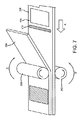
本明細書において開示されるのは、フレーム状境界シールにより取り囲まれた軟質セルユニットの連続生成方法であり、ここでは、非パターン化スペーサにより維持された制御距離だけ分離された2つの軟質基板が連続生成プロセス中に組み合わされ電気光学材料(EOM)でロールフィルされる。本明細書で使用されるように用語「ロールフィルされた」および「ロールフィルする」は、電気光学材料が基板間の制御距離を完全に満たすように1つまたは複数の積層化ローラを使用して軟質基板間の空間またはセルの活性領域をEOMで満たすことを指す。いくつかの実施形態では、ロールフィルは真空を使用することなく実現される(無真空方法)。 Disclosed herein is a method for the continuous generation of soft cell units surrounded by a frame-like boundary seal, where two soft substrates separated by a controlled distance maintained by an unpatterned spacer. Combined during a continuous production process and roll filled with electro-optic material (EOM). As used herein, the terms “roll-filled” and “roll-fill” use one or more laminated rollers so that the electro-optic material completely satisfies the controlled distance between the substrates. In other words, the space between soft substrates or the active region of a cell is filled with EOM. In some embodiments, roll fill is achieved without the use of vacuum (vacuumless method).
一実施形態では、本方法は、第1の(例えば下部)基板と第2の(例えば上部)基板を形成するために軟質プラスチック材料の2つの連続シートを設ける工程と、第1の基板上に電気光学材料を蒸着する工程と、第2の基板と第1の基板とを嵌合し、電気光学材料が第1の基板と第2の基板間の制御距離を満たすようにセル(またはシート)を電気光学材料でロールフィルするために積層化ローラを使用する工程とを含む。境界封止剤はEOMを蒸着する工程の前またはEOMが蒸着された後に塗布され得る。 In one embodiment, the method includes providing two continuous sheets of soft plastic material to form a first (eg, lower) substrate and a second (eg, upper) substrate; The step of depositing the electro-optic material, the second substrate and the first substrate are fitted together, and the cell (or sheet) so that the electro-optic material satisfies the control distance between the first substrate and the second substrate. Using a laminating roller to roll fill the film with an electro-optic material. The boundary sealant can be applied before the step of depositing the EOM or after the EOM is deposited.
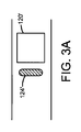
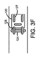
いくつかの実施形態では、境界封止剤はロールフィル工程の前に塗布されるので、本方法は、EOMを蒸着する前に境界封止剤を第1および/または第2または両方の基板上に塗布する工程と、ロールフィル工程の前または後に、境界シールを形成するために境界封止剤を硬化する工程とを含む。この方法では、電気光学材料は境界封止剤の周囲外の領域上に蒸着され得る(図3A)。または、電気光学材料は境界シールの周囲の内部に蒸着され得る(図3B)。他の実施形態では、EOMは、境界封止剤により形成された周囲の内部および外部の両方に1または様々な形状で蒸着され得る(図3C〜F)。この方法は、機械的切断機(例えばxy切断機またはダイ切断機)、またはレーザ切断機、またはそれらの組み合せ、または当該技術分野で知られた任意の他の切断/分離技術を使用して軟質プラスチック材料の2つの連続シートから軟質セルユニットを切断する別の工程を有し得る。 In some embodiments, the boundary sealant is applied prior to the roll fill process, so that the method applies the boundary sealant on the first and / or second or both substrates prior to depositing the EOM. And a step of curing the boundary sealant to form a boundary seal before or after the roll fill step. In this way, the electro-optic material can be deposited on areas outside the perimeter of the boundary sealant (FIG. 3A). Alternatively, the electro-optic material can be deposited inside the periphery of the boundary seal (FIG. 3B). In other embodiments, the EOM can be deposited in one or various shapes both inside and outside the perimeter formed by the boundary sealant (FIGS. 3C-F). This method is flexible using a mechanical cutter (eg, xy cutter or die cutter), or laser cutter, or a combination thereof, or any other cutting / separation technique known in the art. There may be another step of cutting the soft cell unit from two continuous sheets of plastic material.
いくつかのケースでは、境界封止剤が上部基板および下部基板の両方の上に印刷されることが有利かもしれない。この実施形態では、ロールフィルプロセス中、EOMは下部境界封止剤の厳密に上ではなく上部および下部境界封止剤間に流れる。これは、境界封止剤が各基板表面へ接触するということを保証する。これはシールの接着性および安定性を促進する。 In some cases, it may be advantageous for the boundary sealant to be printed on both the upper and lower substrates. In this embodiment, during the roll fill process, the EOM flows between the upper and lower boundary sealants rather than exactly above the lower boundary sealant. This ensures that the boundary sealant contacts each substrate surface. This promotes seal adhesion and stability.
いくつかのケースでは、2つ以上の境界封止剤が塗布され得、例えば、境界シールを設けるために、それぞれが異なる機能(例えば接着機能対非相互作用機能)を提供する2つ以上のタイプの接着剤が採用され得る。 In some cases, more than one boundary sealant may be applied, eg, two or more types, each providing a different function (eg, adhesive function versus non-interacting function) to provide a boundary seal The adhesive may be employed.
他の実施形態では、EOMが最初に塗布され、次に境界封止剤が塗布され、セルがロールフィルされる。一実施形態では、境界封止剤はロールフィル工程の前に硬化される。別の実施形態では、境界封止剤はロールフィル工程後に硬化される。 In other embodiments, EOM is applied first, then boundary sealant is applied, and the cells are roll-filled. In one embodiment, the boundary sealant is cured prior to the roll fill process. In another embodiment, the boundary sealant is cured after the roll fill process.
境界封止剤が存在する場合、境界封止剤は粘度>1000センチポアズ(cP)、>2000cP、>3000cP、>4000cPまたは>5000cPを有する。いくつかの実施形態では、粘度は、10,000cP、20,000cP、30,000cP、40,000cP、50,000cP、60,000cPまたは70,000cP未満である。いくつかの実施形態では、EOM粘度対境界シール粘度の比は、5、6、7、8、9、10、20、30、40または50より大きい。 When present, the boundary sealant has a viscosity> 1000 centipoise (cP),> 2000 cP,> 3000 cP,> 4000 cP or> 5000 cP. In some embodiments, the viscosity is less than 10,000 cP, 20,000 cP, 30,000 cP, 40,000 cP, 50,000 cP, 60,000 cP, or 70,000 cP. In some embodiments, the ratio of EOM viscosity to boundary seal viscosity is greater than 5, 6, 7, 8, 9, 10, 20, 30, 40, or 50.
本方法のいくつかの実施形態では、電気光学材料は化学的に相互作用しないまたは境界封止剤とだけ最小限に相互作用する。いくつかの例では、複数(すなわち、2つ以上)の境界封止剤が一方の基板または両方の基板に塗布され得る。 In some embodiments of the method, the electro-optic material does not interact chemically or minimally interacts only with the boundary sealant. In some examples, multiple (ie, two or more) boundary sealants may be applied to one substrate or both substrates.
別の実施形態では、境界シールは、レーザまたは加熱素子、またはロールフィルされたセル周囲を密閉するために使用される同様な溶着方法を使用して、ロールフィル工程後に生成される。レーザは、活性領域周囲に連続シールを形成するために上部および下部基板を一緒に溶融することができる。レーザはまた、シールを生成しながらシートから個々のセルを同時に切断するように構成され得る。この方法の工程は、第1の(下部)基板および第2の(上部)基板を形成するために軟質プラスチック材料の2つの連続シートを設ける工程と、第1(または第2)の基板上に電気光学材料を蒸着する工程と、電気光学材料で満たされたセルであって非パターン化スペーサにより維持された制御距離を有するセルを形成するために第2の基板と第1の基板とを嵌合するために積層化ローラを使用する工程と、次に、境界シールを形成するとともに軟質プラスチックの2つの連続シートから軟質セルユニットを分離するための形状をレーザ切断する工程とを含む。この方法では、境界封止剤はロールフィル工程の前に塗布されない。むしろ、境界シールはロールフィル工程後に生成される。 In another embodiment, the boundary seal is generated after the roll fill process using a laser or heating element or similar welding method used to seal around the roll filled cell. The laser can melt the upper and lower substrates together to form a continuous seal around the active area. The laser can also be configured to simultaneously cut individual cells from the sheet while producing a seal. The method steps include providing two continuous sheets of soft plastic material to form a first (lower) substrate and a second (upper) substrate, and on the first (or second) substrate. Depositing the second substrate and the first substrate to form a cell filled with the electro-optic material and having a control distance maintained by the non-patterned spacer, the cell being filled with the electro-optic material; Using laminated rollers to combine and then laser cutting a shape to form a boundary seal and separate the soft cell unit from two continuous sheets of soft plastic. In this method, the boundary sealant is not applied prior to the roll fill process. Rather, the boundary seal is created after the roll fill process.
上記方法のうちの任意のものでは、軟質プラスチックのシートが非パターン化スペーサにより予め被覆され得る、または、本プロセスはさらに、非パターン化スペーサを第1の基板、または第2の基板、または両方上へ塗布する工程を含み得る。さらに他の実施形態では、スペーサは電気光学材料内に蒸着され得る。または、そうでなければ、スペーサは第1の基板、第2の基板または両方上のアライメント層内に蒸着され得る。 In any of the above methods, a sheet of soft plastic can be pre-coated with a non-patterned spacer, or the process can further include the non-patterned spacer as a first substrate, a second substrate, or both It may include a step of applying to the top. In yet other embodiments, the spacer can be deposited in the electro-optic material. Alternatively, spacers can be deposited in the alignment layer on the first substrate, the second substrate, or both.
いくつかの例では、スペーサは一方または両方の基板上へ印刷され得る。スペーサの分布は、スペーサが最小回折パターンだけを生成するまたは回折パターンを生成しないようにならなければならない。したがって、用語「非パターン化スペーサ」はランダムパターンまたは非回折生成パターンを有するスペーサを指す。 In some examples, spacers can be printed on one or both substrates. The spacer distribution should be such that the spacer produces only a minimal diffraction pattern or no diffraction pattern. Thus, the term “non-patterned spacer” refers to a spacer having a random pattern or a non-diffracted pattern.
さらに、本明細書で説明するほとんどの例では、スペーサ数(またはスペーサの密度)は>80/平方mmに維持される。 Furthermore, in most examples described herein, the spacer number (or spacer density) is maintained at> 80 / square mm.
上述の実施形態の任意のものでは、基板は、電気光学材料への電圧または電流の印加のための導電層(例えばインジウムスズ酸化物すなわちITO)を含み得る。したがって、軟質プラスチックのシートは導電層により予め被覆され得る、または、本プロセスは導電層を第1の基板と第2の基板へ塗布する工程をさらに含み得る。 In any of the above embodiments, the substrate can include a conductive layer (eg, indium tin oxide or ITO) for application of voltage or current to the electro-optic material. Thus, the sheet of flexible plastic can be pre-coated with a conductive layer, or the process can further include applying the conductive layer to the first substrate and the second substrate.
第1の基板と第2の基板はまた、EOM分子のアライメントを支援するためのアライメント層を含み得る。アライメント層は、軟質プラスチック材料の連続シート上に既に存在し得る(前被覆)。または、本方法は第1の基板、第2の基板または両方上にアライメント層を蒸着する工程を含み得る。アライメント層は、第1または第2の基板シートの全表面へ塗布されてもよいし、第1および第2の基板の一方または両方上に選択的に塗布されてもよい。活性領域は、電気光学材料により満たされ境界シールにより境界をつけられた基板上の領域を指す。選択的塗布は、様々な技術(例えばスクリーン印刷、インクジェット印刷、プレーナ被覆、ローラ加圧、熱加圧、混合物からの相分離、または当該技術分野で知られた他の方法)を使用して実現され得る。いくつかのケースでは、これは所望アライメントを生成し得る自己組織化単層である。 The first substrate and the second substrate may also include an alignment layer to assist in alignment of EOM molecules. The alignment layer can already be present on a continuous sheet of soft plastic material (pre-coating). Alternatively, the method can include depositing an alignment layer on the first substrate, the second substrate, or both. The alignment layer may be applied to the entire surface of the first or second substrate sheet, or may be selectively applied on one or both of the first and second substrates. The active area refers to the area on the substrate that is filled with electro-optic material and bounded by a boundary seal. Selective application can be accomplished using a variety of techniques such as screen printing, ink jet printing, planar coating, roller pressing, heat pressing, phase separation from the mixture, or other methods known in the art. Can be done. In some cases, this is a self-assembled monolayer that can produce the desired alignment.
いくつかの実施形態では、アライメント層は基板間の制御距離を維持するスペーサを含み得る。 In some embodiments, the alignment layer can include spacers that maintain a controlled distance between the substrates.
電気光学材料は、電流または電圧の印加により様替わりされ得る任意の材料を含む。その例としては液晶、電気的着色材料、SPDなどが挙げられる。 Electro-optic materials include any material that can be altered by the application of current or voltage. Examples thereof include a liquid crystal, an electrically colored material, and SPD.
いくつかの実施形態では、電気光学材料は概して、重合可能ではなく非カプセル化状態である。または、1%、2%、3%、4%、5%超の重合可能材料を含まない。いくつかの例では、電気光学材料は非重合可能非カプセル化液晶または液晶−染料混合物を含む。いくつかの例では、電気光学材料はゲスト−ホスト二色性染料−液晶混合物である。いくつかの例では、EOMは非離散的である。特に軟質セルが大きい他の実施形態では、EOMは、基板間の制御距離を維持するのを支援するために、非パターン化スペーサに加えて隔壁の適用により離散的領域に分割または区分化され得る。 In some embodiments, the electro-optic material is generally not polymerizable and is in an unencapsulated state. Or it contains no 1%, 2%, 3%, 4%, more than 5% polymerizable material. In some examples, the electro-optic material comprises a non-polymerizable non-encapsulated liquid crystal or liquid crystal-dye mixture. In some examples, the electro-optic material is a guest-host dichroic dye-liquid crystal mixture. In some examples, the EOM is non-discrete. In other embodiments, particularly where the soft cells are large, the EOM can be divided or segmented into discrete regions by applying partition walls in addition to non-patterned spacers to help maintain the control distance between the substrates. .
電気光学材料は、当該技術分野で知られた任意の蒸着手段を使用することにより第1の基板上の連続膜内に液滴、線、形状、またはシートで蒸着され得る(図3〜図5)。 The electro-optic material can be deposited in droplets, lines, shapes, or sheets in a continuous film on the first substrate by using any deposition means known in the art (FIGS. 3-5). ).
EOMが液晶混合物を含む場合、基板はアライメント層で被覆され得、本方法は、液晶分子(および/または色素)と基板との適切なアライメントを可能にするためにアライメント層を処理する工程を含み得る。本明細書で使用される「処理された」は、液晶の所望アライメントを生成するために当該技術分野で知られた任意数のやり方を含む。例えば、アライメント層ポリイミド(PI)が柔らかい布で物理的に擦られる可能性がある。または、乾燥中にアライメント層ポリイミド(PI)が空気ジェットでアライメントされる可能性がある。UV光などによりアライメントを誘起する光アライメント可能アライメント層もまた知られている。 If the EOM includes a liquid crystal mixture, the substrate can be coated with an alignment layer, and the method includes processing the alignment layer to allow proper alignment of the liquid crystal molecules (and / or dyes) with the substrate. obtain. As used herein, “processed” includes any number of ways known in the art to produce the desired alignment of liquid crystals. For example, the alignment layer polyimide (PI) may be physically rubbed with a soft cloth. Alternatively, the alignment layer polyimide (PI) may be aligned with an air jet during drying. Photoalignable alignment layers that induce alignment by UV light or the like are also known.
いくつかの実施形態では、軟質セルユニットは光学装置である。「光学装置」は、同装置を通して見られる画像の著しい歪み無しにユーザが同装置をのぞくことができために好適な光学特性を有する装置を指す。光学装置は、ユーザが通常、ディスプレイを通して画像を見ないので伝統的ディスプレイと異なる。光学装置の例は、眼鏡、ゴーグル、サンバイザ、保護眼鏡、サンルーフ、窓、窓割りなどを含む。いくつかの例では、光学装置は15%、10%、7%、5%、3%、2%または1%未満の曇価度を有する。 In some embodiments, the soft cell unit is an optical device. “Optical device” refers to a device that has suitable optical properties so that a user can look through the device without significant distortion of the image seen through the device. Optical devices differ from traditional displays because the user typically does not see images through the display. Examples of optical devices include glasses, goggles, sun visors, protective glasses, sunroofs, windows, window splits and the like. In some examples, the optical device has a haze of less than 15%, 10%, 7%, 5%, 3%, 2% or 1%.
いくつかの例では、軟質セルユニットは、様々な電圧の印加により高透過「クリア」状態と低透過「暗」状態とで切り替わることができる液晶−二色性染料混合物を含む光学装置である。このようなゲスト−ホスト液晶−染料混合物は、セルのセルギャップの変動に対するセルの比較的高い耐量のために、本明細書において開示される製造方法に良く適している。 In some examples, the soft cell unit is an optical device that includes a liquid crystal-dichroic dye mixture that can be switched between a high transmission “clear” state and a low transmission “dark” state by application of various voltages. Such guest-host liquid crystal-dye mixtures are well suited for the manufacturing methods disclosed herein because of the relatively high tolerance of the cell to variations in the cell gap of the cell.
本明細書で説明する発明の方法の多くの利点のうちの1つは無真空方法として行われ得るということである。しかし、本方法はまた、必要に応じ真空下で行われ得る。 One of the many advantages of the inventive method described herein is that it can be performed as a vacuumless method. However, the method can also be performed under vacuum if necessary.
本明細書において開示されるのは、境界シールにより取り囲まれ(エッジシールされ)電気光学材料(EOM)で満たされる軟質セルユニットを生成する方法である。概して、本方法は、第1の(例えば下部)基板および第2の(例えば上部)基板を形成するために軟質プラスチック材料の2つの連続シートを設ける工程と、第1の基板上に一定量の電気光学材料を蒸着または分注する工程と、(a)第2の基板と第1の基板とを嵌合し、(b)電気光学材料が第1の基板と第2の基板間の制御距離を満たすように電気光学材料でセルをロールフィルするために積層化ローラを使用する工程とを含む。 Disclosed herein is a method for producing a soft cell unit surrounded by an edge seal (edge sealed) and filled with electro-optic material (EOM). In general, the method includes providing two continuous sheets of flexible plastic material to form a first (eg, lower) substrate and a second (eg, upper) substrate, and a certain amount on the first substrate. A step of evaporating or dispensing the electro-optic material; (a) fitting the second substrate and the first substrate; and (b) controlling distance between the first substrate and the second substrate. Using a laminated roller to roll fill the cell with electro-optic material to satisfy.
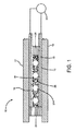
図1は軟質セルユニット10の概要図である。セル10は上部および下部軟質プラスチック基板12、14をそれぞれ含む。用途に依存して、基板は導電層16で被覆され得る。光学的にクリアな導電層は酸化インジウムスズ(ITO)、導電性重合体、導電性ナノワイヤなどを含む。そうでなければまたは加えて、基板はまた、ポリイミドなどのアライメント層18で被覆され得る。
FIG. 1 is a schematic diagram of a
軟質基板12、14は軟質セルユニットを構築するために好適なクリア軟質プラスチック(ポリカーボネート(PC)、ポリカーボネートおよび共重合体混合物、ポリエーテルスルホン(PES)、テレフタル酸ポリエチレン(PET)、三酢酸セルロース(TAC)、ポリアミド、P−酪酸ニトロフェニル(PNB)、ポリエーテルエーテルケトン(PEEK)、ポリエチレンナフタレート(PEN)、ポリエーテルイミド(PEI)、ポリアリレート(PAR)など)または当該技術分野で知られたもので作られる。これらの基板の多くは、例えば三菱プラスチック社または帝人デュポンフィルム社から商業的に入手可能であり、硬皮膜などの様々な被覆と共に標準品となっている。
The
軟質基板12、14はスペーサ24により維持される制御ギャップまたは距離だけ隔てられる。基板間の容積は電気光学材料26により満たされる。
The
スペーサ24は基板間の制御距離またはギャップを維持するために使用される。いくつかの実施形態では、制御ギャップはサイズが3、4、5、6、7、8、9、10、11、12、13、14、15、16、17、18、19、20、30、40、50、60、70、80、90または100μmである。いくつかの例では、制御ギャップは好適にはサイズが5、6、7、8、9または10μmである。「制御」ギャップまたは距離は、基板間の距離の変動が平均でスペーサ直径(制御ギャップを決定する)の30%未満に留まるべきであることを意味する。いくつかの例では、変動はスペーサ直径の25%、20%、15%、10%または5%未満である。
通常、基板間の制御距離を維持するために2種類のスペーサが使用される。1つのカテゴリは、繰り返された幾何学形状の特定パターンを形成するために基板上に意図的に配置または生成されるまたはフォトリトグラフィ/重合化または当該技術分野で知られた同様な方法を使用して生成され回折パターンを生成するスペーサである「パターン化スペーサ」である。その例としては重合体壁が挙げられる。他の例としては、Wen−Tuan Wuらの“P−55:Cell filling of Flexible Liquid Crystal Displays Using One Line Filling and Tilted Roller Pressing”,SID 07 Digest,p393(2007)において使用されるパターン化スペーサが挙げられる。Wuらは、長い列の液晶を生成するために伸ばされるパターン化マイクロ重合体スペーサ(10μm幅×170μm長)を形成するためにフォトリソグラフィ技術を使用する。通常、これらのスペーサはセルギャップより大きい長さおよび幅を有する、すなわち、これらのスペーサは、装置内の可視パターンを生成し得るパターンにおいて>20であるセルギャップ対長辺とのアスペクト比を保有する。 Usually, two types of spacers are used to maintain the control distance between the substrates. One category is intentionally placed or generated on the substrate to form a specific pattern of repeated geometric shapes or uses photolithography / polymerization or similar methods known in the art. It is a “patterned spacer” that is a spacer that generates a diffraction pattern. An example is a polymer wall. As another example, “P-55: Cell filling of Flexible Liquid Crystal Display Using One Line Filling and Tilted Roller Pressing” by Wen-Tuan Wu et al. Can be mentioned. Wu et al. Uses photolithographic techniques to form patterned micropolymer spacers (10 μm wide × 170 μm long) that are stretched to produce long columns of liquid crystals. Typically, these spacers have a length and width greater than the cell gap, i.e., they possess a cell gap to long side aspect ratio that is> 20 in a pattern that can produce a visible pattern in the device. To do.
上記ものとは対照的に、本方法は、基板間の制御距離を維持するために「非パターン化スペーサ」を使用する。本明細書で定義されるように「非パターン化スペーサ」は、回折パターンなどの光学収差などを生成しないようなやり方で位置付けられた場所に無作為に配置(例えば噴霧)または印刷されるスペーサである。本出願の非パターン化スペーサは球状であってもよいし、10/1、5/1、4/1、または3/1未満のアスペクト比(長さ/幅)を有する長方形であってもよい。スペーサは3〜100μm好適には4〜20μmの基板間の距離を維持するために使用される。 In contrast to the above, the method uses “unpatterned spacers” to maintain a controlled distance between the substrates. As defined herein, an “unpatterned spacer” is a spacer that is randomly placed (eg, sprayed) or printed in a location that is positioned in a manner that does not generate optical aberrations such as diffraction patterns. is there. The non-patterned spacer of the present application may be spherical or rectangular having an aspect ratio (length / width) of less than 10/1, 5/1, 4/1, or 3/1. . The spacers are used to maintain a distance between the substrates of 3-100 μm, preferably 4-20 μm.
本明細書で説明される方法の別の特徴はスペーサ数または密度である。本方法は、長いパターン化スペーサが選択位置に配置される場合より大きな密度の小さなスペーサで基板が覆われる場合に、うまく働く。例えば、いくつかの実施形態では、スペーサ数は>80/平方mm(mm2)に維持される。 Another feature of the method described herein is the spacer number or density. The method works well when the substrate is covered with a small spacer of greater density than if a long patterned spacer is placed at a selected location. For example, in some embodiments, the number of spacers is maintained at> 80 / square mm (mm 2 ).
いくつかの実施形態では、スペーサ24は、基板へ予め塗布されてもよいし(例えば、連続シートはスペーサにより予め被覆される)、またはロールツーロールプロセス中に基板へ塗布されてもよく、例えば、スペーサが無作為に配置されるまたは非回折作成パターンで配置される層内に噴霧または塗布され得る。スペーサ24は当該技術領域で知られるように湿式または乾式法を使用して分散され得る。スペーサ24はまた、事前被覆プロセスまたはロールツーロール製造プロセス中にアライメント層内に配置され得る。スペーサはまた、接着層で被覆され得る。
In some embodiments, the
球状スペーサはFERGASONの表題「Encapsulated Liquid Crystal and Method」PCT/米国特許出願第1982/001240号明細書(国際公開第1983/001016号パンフレット)に記載されたような球状カプセル化液晶とは異なるが、これは後者がEOMの容積をカプセル化しないためである。 The spherical spacer is different from the spherical encapsulated liquid crystal as described in the FERGASON title “Encapsulated Liquid Crystal and Method” PCT / US Patent Application No. 1982/001240 (International Publication No. 1983/001016), This is because the latter does not encapsulate the volume of EOM.
いくつかの実施形態では、スペーサ24はアライメント層の内部にまたはその一部として蒸着され得、したがってスペーサ24はアライメント層が一方または両方の基板へ塗布されると塗布される。他の実施形態では、球状スペーサ24は基板上へ蒸着される電気光学材料内に組み込まれ得る。
In some embodiments, the
セル10はさらに、セル内部にEOMを含むとともに外部環境とEOMとの間に障壁を形成する境界シール(エッジシール)27/28を含み、EOMがセルから流出するのを防止するだけでなく環境因子(空気、湿気、デブリ)がセルの内部に入るのを防止する。いくつかの例では、境界シールは基板の一方または両方へ境界封止剤を塗布することにより形成される。境界封止剤は、基板と一緒にされ硬化されると、セル内に含まれる電気光学材料の周囲に境界シールを形成する。図1は、境界封止剤が基板へ塗布される際に基板上の様々な被覆に依存する境界シールの変動を示す。図1において、片側において、境界封止剤27は軟質基板12、14を一緒に密閉する。または、境界シール配置は、アライメント層および/または導電層間のギャップを密閉する境界封止剤28を有するセルの反対側で描かれ得る。特定の配置は境界封止剤を塗布するタイミングおよび方法に依存することになる。
いくつかの実施形態では、境界封止剤は、ロールフィルプロセス中に70,000センチポアズ(cP)未満でありかつ1000cP、2000cP、3000cP、4000cPまたは5000cPを越える粘度を有する。境界封止剤は、接着を支援するために熱が使用される場合に粘度が低下する熱的接着剤だけでなく圧力に応じて粘度が変化する揺変性接着剤も含む。いくつかの実施形態では、EOM粘度対境界シール粘度の比は、5、6、7、8、9、10、20、30、40または50より大きい。いくつかの例では、6000cPの粘度を有する境界シールが成功裡に使用された。境界封止剤の粘度が余りに低ければ境界封止剤は化学的相互作用を促進する処理中にEOMと混じリ得るまたはロールフィルプロセス中に液晶と共に流れて望ましくない位置の基板の表面上に蒸着し得るので、境界封止剤の粘度はセルの品位に影響を与える。境界封止剤が余りにも粘着性であれば、境界シール周囲および近傍の制御ギャップまたは距離は一様ではない。 In some embodiments, the boundary sealant has a viscosity of less than 70,000 centipoise (cP) and greater than 1000 cP, 2000 cP, 3000 cP, 4000 cP or 5000 cP during the roll fill process. Boundary sealants include not only thermal adhesives that decrease in viscosity when heat is used to aid adhesion, but also thixotropic adhesives that change in viscosity as a function of pressure. In some embodiments, the ratio of EOM viscosity to boundary seal viscosity is greater than 5, 6, 7, 8, 9, 10, 20, 30, 40, or 50. In some examples, boundary seals with a viscosity of 6000 cP have been used successfully. If the viscosity of the boundary sealant is too low, the boundary sealant can be mixed with the EOM during a process that promotes chemical interaction, or it can flow with the liquid crystal during the roll fill process and deposit on the surface of the substrate at an undesirable location. As such, the viscosity of the boundary sealant affects cell quality. If the boundary sealant is too tacky, the control gap or distance around and near the boundary seal is not uniform.
いくつかの例では、境界封止剤が長期間(典型的には6か月超、1年超、2年超)にわたり電気光学材料26との化学的相互作用を最小に経験すればまたはそれを経験しなければ有利である。例えば、我々は、封止剤がセルの内部の電気光学材料(例えば液晶)を劣化させるまたはそれと相互作用し得、空気がセル内に忍び込むことを可能にする微小孔を形成し得、したがって気泡または欠陥を形成するということを、長時間をかけて(例えば6か月以上)発見した。いくつかの例では、境界封止剤がEOMまたはその成分に対して非多孔性であれば有利である。例えば、我々は、多孔性境界封止剤がEOM成分の一部を吸着することにより装置の寿命を低下するということを発見した。いくつかの境界封止剤は化学的相互作用を境界シール近傍の液晶の望ましくない変色の形式で提示した。化学的相互作用のいくつかの例では、境界封止剤自体が変色する。これらの相互作用は望ましくない。 In some examples, or if the boundary sealant experiences minimal chemical interaction with the electro-optic material 26 over a long period of time (typically over 6 months, over 1 year, over 2 years) or It is advantageous if you do not experience. For example, we can form a micropore that allows the sealant to degrade or interact with the electro-optic material (eg, liquid crystal) inside the cell, allowing air to sneak into the cell, and thus bubbles Or it discovered that it formed a defect over a long time (for example, 6 months or more). In some instances, it is advantageous if the boundary sealant is non-porous with respect to EOM or its components. For example, we have discovered that porous boundary sealants reduce device life by adsorbing some of the EOM components. Some boundary sealants presented chemical interactions in the form of undesirable discoloration of the liquid crystal near the boundary seal. In some examples of chemical interactions, the boundary sealant itself changes color. These interactions are undesirable.
境界封止剤は、当該技術領域において知られた任意の技術を使用して(例えばブラシ、ローラ、膜またはペレット、噴霧銃、塗布銃、スクリーン印刷、インクジェット印刷、フレキソ印刷、プレーナ被覆、ローラ加圧、熱加圧などを使用して)塗布され得る。これらのすべては手動で行われてもよいし、機械でまたはそれらの組み合せで自動化されてもよい。境界封止剤は、好適な(UV、熱的、化学的、圧力、多液型エポキシ、および/または放射硬化)接着剤、ポリイソブチレンまたはアクリル酸塩ベース封止剤等々、または圧力敏感接着剤、二液型接着剤、湿気硬化接着性などであり得る。他のタイプの境界(エッジ)シールはセルのエッジ全体にわたって接着された金属化箔または他の障壁箔で構成され得る。ハイブリッド放射および熱硬化封止剤(すなわち熱的ポストベークによりUV硬化可能な)がいくつかの利点を提供するということが分かった。例えば、Threebond 30Y−491材料(米国オハイオ州シンシナティのThreebond社の)は、その好ましい水蒸気バリア特性、エッジ封止剤の容易蒸着のための高温における低粘度、良好な濡れ特性、および管理可能硬化特性のために特に有用である。当業者および先進的封止剤に熟知している人々は同等性能を提示する他の封止剤を特定することができるようになる。 The boundary sealant can be obtained using any technique known in the art (eg, brush, roller, film or pellet, spray gun, coating gun, screen printing, ink jet printing, flexographic printing, planar coating, roller coating, etc. Can be applied (using pressure, hot pressing, etc.). All of these may be done manually or automated with a machine or a combination thereof. The boundary sealant is a suitable (UV, thermal, chemical, pressure, multi-part epoxy, and / or radiation curable) adhesive, polyisobutylene or acrylate based sealant, etc., or a pressure sensitive adhesive , Two-part adhesives, moisture-curing adhesives, and the like. Other types of boundary (edge) seals may consist of a metallized foil or other barrier foil adhered across the edges of the cell. It has been found that hybrid radiation and thermoset sealants (ie UV curable by thermal post-bake) provide several advantages. For example, Threebond 30Y-491 material (from Threebond, Cincinnati, Ohio) has its preferred water vapor barrier properties, low viscosity at high temperatures for easy deposition of edge sealants, good wetting properties, and manageable cure properties. Especially useful for. Those skilled in the art and those familiar with advanced sealants will be able to identify other sealants that offer equivalent performance.
セル10は電気光学材料(EOM)で満たされる。電気光学材料は、装置の意図された所望動作特性を有するようにセル両端に印加される電界に応答するとともに電流または電圧の印加により様替わりされ得る任意の材料を含む任意の材料であり得る。例えば、EOMは液晶材料、電気光学材料が電流または電圧の印加により様替わりされ得る電気的着色材料、懸濁粒子装置(SPD)のうちの1つ、またはそれと色素(二色性色素、多色性色素など)など他の添加剤との組み合わせであり得る。好適な実施形態では、EOMはゲスト−ホスト液晶−二色性染料混合物である。
The
いくつかの実施形態では、電気光学材料は概して、重合可能ではなく、非カプセル化状態でありかつ非離散的である。したがって、EOM材料はPDLC、PELC、PSCT、PNLC、NCAPなどの重合体またはカプセル化液晶組成を除外する。 In some embodiments, the electro-optic material is generally not polymerizable, is unencapsulated, and is non-discrete. Thus, EOM materials exclude polymers such as PDLC, PELC, PSCT, PNLC, NCAP or encapsulated liquid crystal compositions.
本明細書で使用されるように、「重合可能でない」は材料の相を固体、半固体またはゲルなどへ変化させることによりEOM層を寸法的に安定させるのに必要な量のいかなる化学成分(例えば重合体)も含まないEOM組成を意味する。 As used herein, “non-polymerizable” means any chemical component (in the amount necessary to dimensionally stabilize the EOM layer by changing the phase of the material to a solid, semi-solid, gel, etc.). For example, it means an EOM composition not including a polymer.
「非離散的」は、カプセル化、重合体壁、重合体網目、パターン化スペーサなどにより離散的かつ別個のコンパートメントに分割されないEOMを意味する。 “Non-discrete” means an EOM that is not divided into discrete and separate compartments by encapsulation, polymer walls, polymer networks, patterned spacers, and the like.
「非カプセル化」は、カプセルの境界または内容積内に含まれないEOMを意味する。カプセルは一定量のEOM材料(液晶など)を閉じ込める格納装置または媒体を指し、したがって「カプセル化EOM」は封入剤(例えば重合体カプセル)内に閉じ込められたまたは含まれる一定量のEOMである。カプセルは球形を有してもよいし、任意の他の好適な形状を有してもよい。カプセル化EOM(例えばカプセル化液晶)は液晶がそれから流れるのを防止するために作られる。カプセル化EOMの例としては重合体網目内部の液晶の液滴からなる重合体分散型液晶(PDLC)が挙げられる。 “Non-encapsulated” means an EOM that is not contained within the boundary or internal volume of the capsule. A capsule refers to a containment device or medium that encloses an amount of EOM material (such as liquid crystal), and thus an “encapsulated EOM” is an amount of EOM that is encapsulated or contained within an encapsulant (eg, a polymer capsule). The capsule may have a spherical shape or any other suitable shape. Encapsulated EOM (eg, encapsulated liquid crystal) is made to prevent liquid crystal from flowing from it. An example of an encapsulated EOM is a polymer dispersed liquid crystal (PDLC) composed of liquid crystal droplets inside a polymer network.
「ロールツーロールプロセス」は、当該ロールの巻き戻しからセルの製造までに基板が経験する全プロセスを意味する。 “Roll-to-roll process” means the entire process that a substrate experiences from unwinding the roll to manufacturing the cell.
例えば、マイクロカプセル化の方法は、表題「Encapsulated liquid crystal and method」米国特許第4,435,047号明細書(1984)および表題「Encapsulated liquid crystal and method」PCT/米国特許出願第1982/001240号明細書(国際公開第1983/001016号パンフレット)においてFERGASONにより説明される。この方法では、樹脂材料は、液晶(LC)材料をカプセル化して離散量のLC材料を含む湾曲球状カプセルを形成するために使用される。これらは、LC材料と、LC材料が溶解しなくLC材料を含む離散的カプセルの形成を可能にする封入剤(例えば樹脂)とを混ぜ合わせることにより作られる。マイクロカプセル化では、液晶は水中で溶解された重合体と混合される。水が蒸発すると、液晶は重合体により囲まれる。多数の小さな「カプセル」が生成され、バルク重合体全体に分散される。カプセル化により製造される材料はNCAPすなわちネマチック曲線配列相と呼ばれる。 For example, the method of microencapsulation is described in the title “Encapsulated liquid crystal and method” US Pat. No. 4,435,047 (1984) and the title “Encapsulated liquid crystal and method” PCT / US Patent Application No. 1982/001240. It is explained by FERGASON in the description (WO 1983/001016 pamphlet). In this method, a resin material is used to encapsulate a liquid crystal (LC) material to form a curved spherical capsule containing a discrete amount of LC material. These are made by mixing the LC material with an encapsulant (eg, a resin) that allows the formation of discrete capsules that do not dissolve and contain the LC material. In microencapsulation, the liquid crystal is mixed with a polymer dissolved in water. As the water evaporates, the liquid crystal is surrounded by the polymer. A number of small “capsules” are produced and dispersed throughout the bulk polymer. The material produced by encapsulation is called NCAP or nematic curve alignment phase.
PDLC、PSCT、相分離(例えば重合化誘起相分離(PIPS))などのPNLCを作成する他の方法が存在する。PIPSにより、LCの液滴は、重合体鎖が分子量で成長するので相分離を介しバルクから排除される、LCは固体重合体壁によりマイクロメートルサイズの液滴内にカプセル化されるようになる。カプセル化されると、液晶は基板が切断されたとしても基板間を流れるまたはそれから漏出することができない。この方法については、例えばSchneiderらのSID Int.Symp.Digest Tech.Papers,vol.36,p.1568(2005)とSchneider t.“New Developments in Flexible Cholesteric Liquid Crystal Displays” Emerging Liquid Crystal Technologies II,Proc.of SPIE,Vol.6487,64870J(2007)とに記載されている。 There are other methods of creating PNLC such as PDLC, PSCT, phase separation (eg polymerization induced phase separation (PIPS)). With PIPS, LC droplets are excluded from the bulk via phase separation as the polymer chains grow in molecular weight, and the LC becomes encapsulated in micrometer-sized droplets by solid polymer walls . Once encapsulated, the liquid crystal cannot flow between or leak out of the substrates even if the substrates are cut. For this method, see, for example, Schneider et al., SID Int. Symp. Digest Tech. Papers, vol. 36, p. 1568 (2005) and Schneider t. “New Developments in Flexible Cholesteric Liquid Crystal Displays”, Emerging Liquid Crystal Technologies II, Proc. of SPIE, Vol. 6487, 64870 J (2007).
電気光学材料が「ゲスト−ホスト」液晶−染料混合物を含む場合、同混合物は液晶「ホスト」溶液内で混合される一定量の1つまたは複数の二色性染料「ゲスト」を含む。液晶「ホスト」分子は、基板の両端に印加される電圧の調整により変更可能な配向の軸を有する。「ゲスト」染料混合物は、液晶ホスト内に溶解され液晶分子の配向とアライメントするとともにその偏光の吸収が色素分子内の吸収ダイポールに対する分極の方向に強く依存する1つまたは複数の二色性色素を含む。印加電圧は、ゲスト−ホスト配向が最大光透過を可能にする第1の状態(ここではクリア状態と呼ばれる)とゲスト−ホスト配向が最小光透過を可能にする第2の状態(ここでは「暗状態」と呼ばれる)と完全クリア状態と完全暗状態間の中間状態の組み合わせとの切り換えを生じる。ゲスト−ホスト混合物の組成に依存して、クリア状態は零電圧(オフ状態)で発生し得る。または、混合物は零電圧(オフ状態)が暗(最小透過)状態に対応するように処方され得る。 Where the electro-optic material includes a “guest-host” liquid crystal-dye mixture, the mixture includes an amount of one or more dichroic dyes “guests” that are mixed in a liquid crystal “host” solution. Liquid crystal “host” molecules have an axis of orientation that can be altered by adjusting the voltage applied across the substrate. A “guest” dye mixture contains one or more dichroic dyes that are dissolved in a liquid crystal host to align with the orientation of the liquid crystal molecules and whose absorption is strongly dependent on the direction of polarization relative to the absorbing dipole in the dye molecule. Including. The applied voltage includes a first state where the guest-host orientation allows maximum light transmission (referred to herein as a clear state) and a second state where the guest-host orientation allows minimum light transmission (here “dark”). Switching between a completely clear state and a combination of intermediate states between a completely dark state. Depending on the composition of the guest-host mixture, the clear state can occur at zero voltage (off state). Alternatively, the mixture can be formulated so that zero voltage (off state) corresponds to the dark (minimum transmission) state.
ゲスト−ホスト液晶−染料混合物を含むセルは、セルギャップの変動に対するそれらのより大きな耐性(すなわち、セルギャップの公差または変動が<1%に保たれなければならない偏光子ベースのLC装置など相遅延に依存するセルと比較して、セルはより寛容であり、セルギャップがわずかな変動(+/−5%、10%、15%、20%、25%、またはさらには30%などの許容限度内の)を有してもうまく機能し得る)のために、本明細書で説明する方法による製造に特に良く適している。 Cells containing guest-host liquid crystal-dye mixtures are more resistant to their cell gap variations (ie, cell-gap tolerance or variation must be kept <1%, such as polarizer-based LC devices). Compared to cells that depend on the cell, the cell is more forgiving and the cell gap varies slightly (+/− 5%, 10%, 15%, 20%, 25%, or even 30% acceptable limits Are particularly well suited for production by the methods described herein.
いくつかの実施形態では、上に説明されたゲスト−ホスト液晶−染料混合物は光学装置内の光を減衰するために使用される。「光学装置」は、ユーザが物体を見ることができる主として透過性装置(例えば一対の眼鏡、ゴーグル、サンバイザ、または窓)であるセルを指す。 In some embodiments, the guest-host liquid crystal-dye mixture described above is used to attenuate light in an optical device. “Optical device” refers to a cell that is primarily a transmissive device (eg, a pair of glasses, goggles, sun visor, or window) through which a user can see an object.
零電圧(オフ状態)においてクリア(最大透過)状態を有する装置は例えば次の場合に実現され得る:ゲスト−ホスト液晶−染料混合物は電圧が印可されていないとホメオトロピックアライメント(すなわち基板に垂直なアライメント)を有し、液晶ホストは負の誘電体異方性を有し、二色性色素は正の二色性を有する(すなわち、分極が色素分子の長い分子軸と平行な場合に最大吸収を、分極が同軸に対して垂直な場合に最小吸収を有する)場合。このような装置では、電圧が印加されると(ON状態)、ゲスト−ホスト混合物は平面またはホモジニアスアライメント(すなわち、基板と平行アライメント)を取り、最大光吸収(暗)状態になる。このような構成は、明るい光が存在する場合に印加された電圧に応じて装置を「暗くする」ことが望ましいかもしれない例えばゴーグル、眼鏡、サンバイザなどにおいて使用され得る。他の用途は窓(車両、建物、航空機など)およびサンルーフ/ムーンルーフなどを含む。 A device having a clear (maximum transmission) state at zero voltage (off state) can be realized, for example, when: a guest-host liquid crystal-dye mixture is homeotropic alignment (ie perpendicular to the substrate) when no voltage is applied. The liquid crystal host has a negative dielectric anisotropy, and the dichroic dye has a positive dichroism (ie, maximum absorption when the polarization is parallel to the long molecular axis of the dye molecule) With minimal absorption when the polarization is perpendicular to the coaxial). In such a device, when a voltage is applied (ON state), the guest-host mixture takes a planar or homogeneous alignment (ie parallel alignment with the substrate) and is in a maximum light absorption (dark) state. Such a configuration may be used in eg goggles, glasses, sun visors etc. where it may be desirable to “darken” the device in response to an applied voltage in the presence of bright light. Other applications include windows (vehicles, buildings, aircraft, etc.) and sunroof / moon roofs.
他の例では、印加電圧がオフである場合にゲスト−ホスト液晶−染料混合物が暗状態の平面アライメント(ホモジニアスアライメント)を有し得、電圧が印加された場合にクリア状態のホメオトロピックアライメントを有し得るように逆のアライメントが実施され得る。これは、正の二色性を有する色素と正の誘電異方性を有する液晶材料とを併用してアライメント層のプレーナ表面処理を使用することにより実現され得る。このような構成は、装置が通常「暗」状態にあるが電圧の印加によりクリア状態へ切り替わることができることが望ましい場合(例えば窓またはサンルーフ)に使用され得る。 In another example, the guest-host liquid crystal-dye mixture can have a dark planar alignment (homogeneous alignment) when the applied voltage is off and have a clear homeotropic alignment when a voltage is applied. A reverse alignment can be performed as is possible. This can be achieved by using a planar surface treatment of the alignment layer in combination with a dye having positive dichroism and a liquid crystal material having positive dielectric anisotropy. Such a configuration can be used when the device is normally in a “dark” state, but it is desirable to be able to switch to a clear state by application of a voltage (eg, a window or sunroof).
最後に、セル10はセル両端の電界または電圧の印加のために制御回路30へ接続され得る。電圧源はACまたはDCのいずれでもよい。
Finally, the
セル10を作るロールフィル方法の一例が図2に示される。この例では、2つの軟質プラスチックのロール100、102が上部基板104と下部基板106とをそれぞれ形成するために使用される。プラスチックの連続シートは、プラスチックシートを回転し一組の積層化ローラ110、110’の方向へ移動させる一組のローラ(108)上へ配置される。この例では、軟質プラスチックの各連続シートは既にITO導電層で被覆されている。一組の塗布器112、112’が、ポリイミドアライメント層116、116’を上部および下部基板104、106上へ塗布するために使用される。噴霧塗布器117が、球状スペーサ118の層を下部基板106上へ塗布するために使用される。
An example of a roll fill method for making the
図2はスペーサが下部基板へ塗布されていることを示すが、他の例では、スペーサは上部基板、または上部基板と下部基板の両方へ塗布され得る。スペーサはロールツーロールプロセスの前に単一ロールまたは両ロールの基板へ塗布され得る。スペーサ18はまた、当該技術領域において知られた任意の方法(湿式または乾式噴霧、印刷、または溶液中での湿式被覆を含む)を使用してロールツーロールプロセス中に塗布され得る。
Although FIG. 2 shows that the spacer is applied to the lower substrate, in other examples, the spacer can be applied to the upper substrate or both the upper and lower substrates. Spacers can be applied to single roll or both roll substrates prior to the roll-to-roll process. The
いくつかの例では、スペーサはアライメント層の一部として埋め込まれ塗布され得る。さらに他の例では、スペーサは、EOMが基板上へ蒸着される際にEOMの一部として埋め込まれ塗布され得る。 In some examples, the spacer may be embedded and applied as part of the alignment layer. In yet another example, the spacer may be embedded and applied as part of the EOM as the EOM is deposited on the substrate.
スクリーン印刷機119は、基板が方向Aへ転がると境界封止剤パターン120を下部基板106上へ印刷する。いくつかの実施形態では、スクリーン印刷機は回転スクリーン印刷機であり、上部基板、下部基板または両方の基板は境界封止剤で印刷される。
When the substrate rolls in direction A, the
液晶/染料混合物124などのEOMのストリップまたは線は、境界封止剤120により形成された領域の近傍であるがその外側の下部基板106上へ蒸着針125を使用することにより蒸着される。本明細書でまた企図されるのは、EOM124が境界封止剤120の前に蒸着される方法である。
An EOM strip or line, such as a liquid crystal /
次に、積層化ローラ110、110’が、上部基板104と下部基板106とを一緒にして「嵌合する」するために使用される。ローラからの圧力は、EOM124を押し、境界シール120の上を転がして境界封止剤120の境界内部の「活性」領域内に入れ、こうしてEOM124で満たされたセル130を形成する。上部および下部基板の「嵌合」は上部基板104を境界封止剤120に接触させ、さらに上部および下部基板をスペーサの幅だけ分離するスペーサ118に接触させる。スペーサ118は上部および下部基板間の制御距離または「ギャップ」(次にEOM124で満たされる)を維持する。
Next,
最後に、境界封止剤120は硬化装置128により硬化され、セル130は転がるプラスチックシートから切断され除去される。しかし、最初にセルを切断し分離し、次に、UV光、熱、圧力、化学的相互作用、湿気、またはそれらの組み合せ、または境界封止剤を硬化するための任意の手段を使用することにより境界シールを硬化することが可能である。セルを含む嵌合された基板の部分は、セルを含むシートに切断され得る。次に、セルは機械的または光学的のいずれかの他の方法により切り出され得る。機械的手段は、ダイ切断、x−yカミソリ刃による切断、またははさみなどを含む。光学的切断はレーザ切断などを含む。
Finally, the
電気光学材料は、図3A〜3Bに示すように、境界シールの周囲の内部または外部のいずれかの上に蒸着され得る。他の例では、EOMは境界封止剤の内部と外部の両方の様々な領域内に蒸着され得る(図3C〜3F)。図3に示すように、電気光学材料は液滴、線または形状で選択的に蒸着され得る。 The electro-optic material can be deposited either on the inside or the outside of the perimeter seal, as shown in FIGS. In other examples, the EOM can be deposited in various regions both inside and outside the boundary sealant (FIGS. 3C-3F). As shown in FIG. 3, the electro-optic material can be selectively deposited in droplets, lines or shapes.
EOMの一部またはすべてが境界封止剤周囲外に蒸着されれば、積層化ローラからの圧力が、活性セル領域を満たすために、EOMに境界封止剤の上を転がらせる。したがって、電気光学混合物と封止剤との間の最小相互作用を有し、したがって一方の機能が他方の機能と干渉しないことが好ましい。 If some or all of the EOM is deposited outside the periphery of the boundary sealant, the pressure from the lamination roller causes the EOM to roll over the boundary sealant to fill the active cell area. Accordingly, it is preferred to have a minimum interaction between the electro-optic mixture and the sealant and thus one function does not interfere with the other.
無境界処理
図4に示す製造方法の別の実施形態では、いかなる境界シールもロールフィル工程の前に塗布されない。むしろ、一定量のEOM270が基板272上へ塗布され、次に、要望により予め被覆された2つの基板272、274が一緒にされEOMでロールフィルされ、それらの分離性は一方または両方の基板上でスペーサにより維持される。ロールフィルの工程は単一または二重ローラにより行われ得る。
Borderless treatment In another embodiment of the manufacturing method shown in FIG. 4, no boundary seal is applied prior to the roll fill process. Rather, a certain amount of
エッジシール278は、形状を切断し境界シールを同時に生成するように働くレーザ切断またはレーザ溶着装置279により生成され、EOM充填軟質セルユニット280がプラスチックの連続シートの残りから生成され分離される。または、嵌合された基板からセルを分離することなく基板同士が最初に溶着され、次にセルがシートの残りから切断および/または分離される二段法が採用され得る。溶着工程はレーザ、熱または両方の組み合わせにより行われ得る。
The
図5は、図4に示す無境界方法におけるEOM蒸着の様々なパターンを示す。図から分かるように、EOMは、離散的パターンで、または一方(または両方)の基板上の領域のほとんどを覆う「シート」として、蒸着される。 FIG. 5 shows various patterns of EOM deposition in the borderless method shown in FIG. As can be seen, the EOM is deposited in a discrete pattern or as a “sheet” covering most of the area on one (or both) substrates.
本明細書で説明する方法のうちのいかなるものも大面積装置(すなわち30cm2、40cm2または50cm2より大きな面積を有する任意のもの、または10cm長を越える任意のセル)を製造するために使用され得る。 Any of the methods described herein can be used to manufacture large area devices (ie, any having an area greater than 30 cm 2 , 40 cm 2 or 50 cm 2 , or any cell over 10 cm long). Can be done.
いくつかの実施形態では、本プロセスは「膜誘導器」を使用することなく行われる。「膜誘導器」は、通常は上部基板を適切なアライメントに誘導するために使用される剛性シートである。このような上部膜誘導器は、Wuらの“P−55:Cell filling of Flexible Liquid Crystal Displays Using One Line Filling and Tilted Roller Pressing”,SID 07 Digest,p393(2007)に記載される。しかし、その使用は、このような「誘導装置」が上部基板に容易に接触しそれを擦り、したがって上部基板を引っ掻くまたは導電性および/またはアライメント層などの被覆をこすり落とし得るという欠点を有する。 In some embodiments, the process is performed without the use of a “membrane inductor”. A “membrane inductor” is a rigid sheet that is typically used to guide the upper substrate to proper alignment. Such an upper membrane inductor is described in Wu et al., “P-55: Cell filling of Flexible Liquid Crystals Displaying One Line Filing and Tilted Roller Pressing”, SID 07 Digest 7 (page 39). However, its use has the disadvantage that such a “guidance device” can easily contact and rub the upper substrate, thus scratching the upper substrate or scraping the coating such as the conductive and / or alignment layers.
本明細書で説明する方法はまた、一方または両方の基板を運ぶために「プレート」を使用することなく実施され得る。例えば、Wuらにおいては、下部基板は「ステージ」またはプレートへ固定される。このプレートは製造されるセルのサイズの制限因子になり得る。大きなセル(例えばディスプレイ、窓)を生成するために、大きなプレートが必要とされる。これはクリーンルーム環境内の貴重な空間を占める。加えて、各異なるサイズのセルは異なるサイズのプレートを必要とするだろう。さらに、基板を移動するためにステージを使用することは、セルが正しく動作するために基板間のギャップが低偏差(例えば+/−15%または1〜3μmの公差)でもって一定に維持される必要があるので、大きな軟質セル製造では問題である。但し、ステージ自体はしばしば完全に平坦ではないので、より大きなセルでは、このような低公差を維持することはますます困難になる。 The methods described herein can also be practiced without using “plates” to carry one or both substrates. For example, in Wu et al., The lower substrate is fixed to a “stage” or plate. This plate can be a limiting factor for the size of the cell being manufactured. Large plates are required to create large cells (eg, displays, windows). This takes up valuable space within the clean room environment. In addition, each different sized cell will require a different sized plate. Furthermore, using a stage to move the substrate keeps the gap between the substrates constant with low deviations (eg +/− 15% or 1 to 3 μm tolerance) for the cell to operate correctly. This is a problem in large soft cell manufacturing because it is necessary. However, since the stage itself is often not perfectly flat, it becomes increasingly difficult to maintain such low tolerances in larger cells.
ここで説明するロールフィル方法がプレートやステージを使用しない場合、プラスチック基板の運動はローラの運動により可能にされる。したがって、本方法は様々なサイズのセルを迅速かつ容易に生成するようにされ得る。例えば、1つの長さのセルが作成され得、まさしく次のセルは異なる長さであり得、いかなる設備一新工程も材料浪費も無い。 If the roll fill method described here does not use plates or stages, the movement of the plastic substrate is made possible by the movement of the rollers. Thus, the method can be adapted to quickly and easily generate cells of various sizes. For example, one length of cell can be created, and the next cell can be of a different length, without any equipment renewal process or material waste.
2つの基板間の嵌合(積層化)工程は1つまたは2つのローラを使用して実現され得る。2つのローラを使用する場合、2つのローラ間の圧力および/またはギャップが2つの基板を積層するために使用される。ローラはゴム、金属またはそれらの組み合せで作製され得、例えば、一方のローラはゴムを有し、他方のローラは金属外側層を有する。ロールツーロール製作において、損傷を回避するためにローラの直径とプラスチック強度とが調節されなければならないということは当該技術領域ではよく知られている。 The mating (lamination) process between two substrates can be realized using one or two rollers. When using two rollers, the pressure and / or gap between the two rollers is used to laminate the two substrates. The rollers can be made of rubber, metal, or combinations thereof, for example, one roller has rubber and the other roller has a metal outer layer. It is well known in the art that in roll-to-roll fabrication, the roller diameter and plastic strength must be adjusted to avoid damage.
積層化が単一ローラを使用して実施される場合、ウェブ内の張力が圧力の主要な源である。一例では、2つの基板はそれぞれローラを動き回れ得るようにされ、積層化圧力がロール上の張力のおかげで実現される。 When lamination is performed using a single roller, the tension in the web is the primary source of pressure. In one example, the two substrates are each allowed to move around the roller, and the lamination pressure is achieved thanks to the tension on the roll.
基板は、プロセス中の引っ掻きに対する保護のために、またはその厚さを増加するために、または抗張力を変えるために保護膜が予め積層化され得る。さらに、基板は、防曇、反射防止、硬皮膜、スリップ層など機能性被覆により前処理され得る。 The substrate may be pre-laminated with a protective film to protect against scratching during the process, or to increase its thickness, or to change the tensile strength. Further, the substrate can be pretreated with a functional coating such as antifogging, antireflection, hard coating, slip layer.
以下の実施例では、どのように軟質液晶セルが本明細書で説明する方法に従って製造されるかについて説明する。 The following examples describe how a soft liquid crystal cell is manufactured according to the method described herein.
実施例1
●ITOとアライメント層PIにより予め被覆された2つの基板が、一方が上部基板を形成し他方は下部基板を形成する一組のローラ上に配置される、
●下部基板は非パターン化スペーサで噴霧される、
●境界封止剤が下部基板上へ印刷される、
●液晶/染料混合物の線が境界封止剤の周囲外に蒸着される、
●ローラは、上部および下部基板を一緒にし、境界封止剤の周囲の内部の活性領域を液晶/染料混合物でロールフィルするために使用される、
●境界封止剤はエッジシールを形成するためにUV硬化される。
Example 1
Two substrates pre-coated with ITO and alignment layer PI are placed on a set of rollers, one forming the upper substrate and the other forming the lower substrate,
● The lower substrate is sprayed with non-patterned spacers,
● Boundary sealant is printed on the lower substrate,
● A line of liquid crystal / dye mixture is deposited outside the boundary sealant,
● Rollers are used to bring the upper and lower substrates together and roll fill the active area around the boundary sealant with a liquid crystal / dye mixture,
The boundary sealant is UV cured to form an edge seal.
実施例2−単一ローラ
図6に示す別の実施例では、下部基板は、セル120をロールフィルするために使用される移動プレート150および単一ローラ(110’)上に配置され、それへ固定され得る。この実施例では、移動ローラ110’がプレートおよび/または下部基板の方向Aの運動を引き起こし得るか、または移動プレート150が下部基板を移動し、ローラを方向Bに転回させ、基板同士を対にし、セルをロールフィルするかのいずれかである。
Example 2-Single Roller In another embodiment shown in FIG. 6, the lower substrate is placed on and over a moving
実施例3−二重ローラ(上部および下部)
この実施例では(図7)、一組の上部および下部ローラ200、202が、上部軟質基板204を下部軟質基板206へ嵌合するまたはこれらを対にするために使用される。境界封止剤208が下部基板206へ塗布される。ローラ200、202はローラ自身を介し軟質基板をウェブ方向Aに引っ張る。転回中、蒸着された電気光学混合物210は、2つの基板204、206が対にされている間に、2つの基板204、206間に生成された制御ギャップを同時に満たす。
Example 3 Double Roller (Upper and Lower)
In this embodiment (FIG. 7), a set of upper and
この方法は連続的ロールツーロール型プロセスにおいて採用され得る。基板上に蒸着されたOEMの量は、本プロセスがより多くのOEMが使用されてもうまく働き一定量のEOMがロールフィル工程中に境界シールの上を流れる結果になるので注意深く測定される必要はない。これは、セルが完全に満たされるが境界封止剤はLCに最小限度に接触するだけであろうようにセルを満たすために必要とされる極めて正確な量のOEMの蒸着を必要とした従来の製造方法を越える利点である。 This method can be employed in a continuous roll-to-roll process. The amount of OEM deposited on the substrate needs to be carefully measured as the process works well even when more OEMs are used, resulting in a certain amount of EOM flowing over the boundary seal during the roll fill process. There is no. This required the deposition of a very accurate amount of OEM required to fill the cell so that the cell was completely filled but the boundary sealant would only touch LC minimally. This is an advantage over the manufacturing method.
実施例4−二重ローラ(左および右)
この実施例では、一組の左右ローラ250、252が、基板を垂直下方向に移動させながら軟質基板254と軟質基板256とを対にするために使用される(図8)。
Example 4-Double roller (left and right)
In this embodiment, a set of left and
実質的に、前述の方法の上部および下部ローラは今や並んで配置される。違いは、この新しい配置では基板254、256が2つの異なる水平方向E、Fからそれぞれ一緒に来るということである。ローラはローラ自身を介し軟質基板を垂直下方向であるウェブ方向Gに引っ張る。転回中、前述のように、蒸着されたEOMは、2つの基板が対にされている間に、2つの基板間に生成された制御ギャップを同時に満たす。このセットアップは、基板上のいかなるアライメント層も印刷またはパターン化することを容易にし、および/または追加処理工程が一方または両方のプラスチックシート/基板に対し行われ得るようにするであろう。
In effect, the upper and lower rollers of the aforementioned method are now arranged side by side. The difference is that in this new arrangement, the
実施例5
別の実施例では、基板の2つのロールがそれぞれローラ上に配置される。各ロールは三菱プラスチック社の0.076mm(3mil)PETである。基板ロールはMaterion社による導電層(ITO)で予め被覆される。次に、ITO被覆基板はポリイミドアライメント層(Nissan Chemicals社の5661)で被覆される。直径6マイクロメートルのShinshikyuEWプラスチック球(Hiko Industrial社、香港)が被覆処理中にポリイミド内に混合され、基板ロールの少なくとも一方内に存在する。ローラはロールツーロールプロセス中に基板のロールを巻き戻す。1つの巻き戻されたロールが上部基板になり、第2番目は下部基板になる。基板はロールツーロールプロセス中約1.27cm(0.5インチ)/秒から約2.54cm(10インチ)/秒のウェブ速度で移動する。各基板は当該境界封止剤印刷機を有する。この場合、これらの印刷機は回転スクリーン印刷機である。回転スクリーン印刷機は境界封止剤(Loctite3108)を上部および下部基板の活性面のそれぞれの上に印刷する。活性面は完成セル内のEOMに接することになる面である。回転印刷機は境界封止剤を約5マイクロメートル〜約100マイクロメートル(好適には約5マイクロメートル〜約40マイクロメートル)の高さで印刷するだろう。回転印刷後、EOMは注射器および針分注器により下部基板の活性面上に蒸着される。EOMはゲスト−ホスト二色性染料−液晶混合物(AMI577)である。一組の上部および下部積層化ローラは、上部境界封止剤が下部境界封止剤とアライメントされ、EOMが上部および下部活性面の両方と接触しロールフィルプロセス中に全内部境界封止剤領域を満たすように、上部および下部基板同士を嵌合する。積層化ローラは、積層化中に基板両端に定圧を印加する加圧ローラとなるように構成される、または、上部積層化ローラが下部積層化ローラからある設定距離で離間され、上部および下部基板の間の制御ギャップおよびスペーサを加圧することなく上部および下部基板を嵌合できるようにするギャップ設定ローラとなるように構成される。嵌合された基板は、紫外線、熱、またはUVおよび熱硬化の組み合わせにより、積層化後に硬化される。次に、硬化基板は、追加処理のためにロールから切断されシートにされる。
Example 5
In another embodiment, two rolls of substrate are each placed on a roller. Each roll is 0.076 mm (3 mil) PET from Mitsubishi Plastics. The substrate roll is pre-coated with a conductive layer (ITO) from Material. The ITO coated substrate is then coated with a polyimide alignment layer (5661 from Nissan Chemicals). A 6 micrometer diameter Shinshiyu EW plastic sphere (Hiko Industrial, Hong Kong) is mixed into the polyimide during the coating process and is present in at least one of the substrate rolls. The roller unwinds the roll of substrate during the roll-to-roll process. One unrolled roll becomes the upper substrate and the second becomes the lower substrate. The substrate moves at a web speed of about 0.5 inches / second to about 10 inches / second during the roll-to-roll process. Each substrate has the boundary sealant printer. In this case, these printers are rotary screen printers. The rotary screen printer prints boundary sealant (Loctite 3108) on each of the active surfaces of the upper and lower substrates. The active surface is the surface that will contact the EOM in the completed cell. The rotary printer will print the boundary sealant at a height of about 5 micrometers to about 100 micrometers (preferably about 5 micrometers to about 40 micrometers). After rotational printing, the EOM is deposited on the active surface of the lower substrate by a syringe and needle dispenser. EOM is a guest-host dichroic dye-liquid crystal mixture (AMI577). A set of upper and lower laminated rollers has the upper boundary sealant aligned with the lower boundary sealant and the EOM contacts both the upper and lower active surfaces so that the entire inner boundary sealant area during the roll fill process The upper and lower substrates are fitted together so as to satisfy the above. The laminating roller is configured to be a pressure roller that applies constant pressure to both ends of the substrate during laminating, or the upper laminating roller is separated from the lower laminating roller by a set distance, and the upper and lower substrates It is configured to be a gap setting roller that allows the upper and lower substrates to be fitted without pressurizing the control gap and spacers between them. The mated substrate is cured after lamination by ultraviolet light, heat, or a combination of UV and heat curing. The cured substrate is then cut from the roll into a sheet for additional processing.
Claims (20)
前記第1の基板と前記第2の基板を形成するために軟質プラスチック材料の2つの連続シートを設ける工程と、
非カプセル化・非重合体状態であり1%未満の重合可能材料を含む電気光学材料を少なくとも一方の基板上に蒸着する工程と、
前記電気光学材料が前記第1の基板と前記第2の基板の間の前記制御距離を完全に満たすように、1つまたは複数の積層化ローラを使用することにより前記軟質セルを前記電気光学材料でロールフィルしながら前記第1の基板と前記第2の基板を対にする工程と、を含む方法。 A method for producing a soft cell unit surrounded by a boundary seal and filled with an electro-optic material, the first and second substrates being separated by a control distance maintained by a spacer, said method Is
Providing two continuous sheets of soft plastic material to form the first substrate and the second substrate;
Depositing an electro-optic material in a non-encapsulated, non-polymeric state and containing less than 1% polymerizable material on at least one substrate;
Using one or more laminated rollers, the electro-optic material makes the electro-optic material the electro-optic material so that the electro-optic material completely satisfies the control distance between the first substrate and the second substrate. And pairing the first substrate and the second substrate while roll-filling.
Applications Claiming Priority (3)
| Application Number | Priority Date | Filing Date | Title |
|---|---|---|---|
| US201462080630P | 2014-11-17 | 2014-11-17 | |
| US62/080,630 | 2014-11-17 | ||
| PCT/US2015/058737 WO2016081185A1 (en) | 2014-11-17 | 2015-11-03 | Method for producing a flexible electro-optic cell |
Publications (3)
| Publication Number | Publication Date |
|---|---|
| JP2017534083A true JP2017534083A (en) | 2017-11-16 |
| JP2017534083A5 JP2017534083A5 (en) | 2018-12-13 |
| JP7027165B2 JP7027165B2 (en) | 2022-03-01 |
Family
ID=56014388
Family Applications (1)
| Application Number | Title | Priority Date | Filing Date |
|---|---|---|---|
| JP2017526079A Active JP7027165B2 (en) | 2014-11-17 | 2015-11-03 | How to generate a soft electro-optic cell |
Country Status (8)
| Country | Link |
|---|---|
| US (1) | US10401690B2 (en) |
| JP (1) | JP7027165B2 (en) |
| KR (1) | KR102413786B1 (en) |
| CN (2) | CN117850105A (en) |
| DE (1) | DE112015005187T5 (en) |
| GB (1) | GB2546935B (en) |
| TW (1) | TWI741970B (en) |
| WO (1) | WO2016081185A1 (en) |
Cited By (1)
| Publication number | Priority date | Publication date | Assignee | Title |
|---|---|---|---|---|
| JP2020030288A (en) * | 2018-08-21 | 2020-02-27 | 大日本印刷株式会社 | Dimmer unit and dimming member |
Families Citing this family (11)
| Publication number | Priority date | Publication date | Assignee | Title |
|---|---|---|---|---|
| US11435610B2 (en) | 2014-11-17 | 2022-09-06 | Alphamicron Incorporated | Method for producing a flexible electro-optic cell |
| US10843535B1 (en) * | 2015-12-01 | 2020-11-24 | Apple Inc. | System and method for dynamic privacy and window tinting |
| KR102056595B1 (en) * | 2015-12-17 | 2019-12-17 | 주식회사 엘지화학 | Liquid crystal window and optical member comprising it |
| US10326205B2 (en) * | 2016-09-01 | 2019-06-18 | Wafer Llc | Multi-layered software defined antenna and method of manufacture |
| CN115308949A (en) * | 2016-12-22 | 2022-11-08 | 大日本印刷株式会社 | Light control member, method for manufacturing light control member, light controller, and vehicle |
| CN206710760U (en) * | 2017-05-12 | 2017-12-05 | 北京京东方光电科技有限公司 | A kind of shooting part, display device |
| KR102489356B1 (en) * | 2017-07-31 | 2023-01-18 | 다이니폰 인사츠 가부시키가이샤 | Laminated glass, manufacturing method of laminated glass |
| CN108594042B (en) * | 2018-04-23 | 2021-04-02 | 张家港康得新光电材料有限公司 | Online electrification detection method and detection system for PDLC film |
| CN109143653A (en) * | 2018-11-07 | 2019-01-04 | 深圳秋田微电子股份有限公司 | Flexible liquid crystal device and preparation method thereof |
| WO2020237568A1 (en) * | 2019-05-30 | 2020-12-03 | 京东方科技集团股份有限公司 | Manufacturing apparatus and method for flexible liquid crystal display screen |
| CN110501774A (en) * | 2019-07-19 | 2019-11-26 | 华为机器有限公司 | The method of rotatory polarization piece and manufacture rotatory polarization piece, light emitting device |
Citations (15)
| Publication number | Priority date | Publication date | Assignee | Title |
|---|---|---|---|---|
| JPS58140718A (en) * | 1982-02-17 | 1983-08-20 | Hitachi Ltd | Method and apparatus for manufacturing liquid crystal display element |
| JPH01293316A (en) * | 1988-05-20 | 1989-11-27 | Toray Ind Inc | Spacer for liquid crystal display and production thereof |
| JPH05232472A (en) * | 1992-02-20 | 1993-09-10 | Seiko Instr Inc | Production of electrooptical device |
| JPH07325280A (en) * | 1994-04-08 | 1995-12-12 | Dainippon Printing Co Ltd | Formation of liquid crystal/high polymer composite optical element |
| JPH10186384A (en) * | 1996-11-08 | 1998-07-14 | Sony Corp | Liquid crystal element, its production, and manufacturing device therefor |
| JPH11119180A (en) * | 1997-10-09 | 1999-04-30 | Fuji Photo Film Co Ltd | Production of liquid crystal display device |
| JP2001042349A (en) * | 1999-07-27 | 2001-02-16 | Minolta Co Ltd | Liquid crystal display device |
| JP2003270642A (en) * | 2002-03-18 | 2003-09-25 | Minolta Co Ltd | Liquid crystal display device |
| JP2004258673A (en) * | 2004-04-20 | 2004-09-16 | Semiconductor Energy Lab Co Ltd | Method for manufacturing liquid crystal display device |
| JP2006349899A (en) * | 2005-06-15 | 2006-12-28 | Nippon Electric Glass Co Ltd | Spacer for liquid crystal display element and liquid crystal display element |
| WO2008007715A1 (en) * | 2006-07-14 | 2008-01-17 | Asahi Glass Company, Limited | Liquid crystal optical device and process for manufacturing the same |
| WO2008007788A1 (en) * | 2006-07-14 | 2008-01-17 | Asahi Glass Company, Limited | Structure and process for producing the same |
| WO2008041268A1 (en) * | 2006-09-29 | 2008-04-10 | Fujitsu Limited | Liquid crystal display element, process for producing the same and electronic paper having the element |
| US20110308076A1 (en) * | 2010-06-22 | 2011-12-22 | Yeon Heui Nam | Apparatus for manufacturing liquid crystal display panel |
| JP2012063761A (en) * | 2010-08-17 | 2012-03-29 | Semiconductor Energy Lab Co Ltd | Liquid crystal device and manufacturing method for liquid crystal device |
Family Cites Families (37)
| Publication number | Priority date | Publication date | Assignee | Title |
|---|---|---|---|---|
| US4435047A (en) | 1981-09-16 | 1984-03-06 | Manchester R & D Partnership | Encapsulated liquid crystal and method |
| US4647157A (en) * | 1984-12-04 | 1987-03-03 | Polaroid Corporation | Fluoroelastomeric sealants for liquid crystal cells |
| US4904056A (en) * | 1985-07-19 | 1990-02-27 | General Electric Company | Light blocking and cell spacing for liquid crystal matrix displays |
| US5514504A (en) | 1991-01-31 | 1996-05-07 | Dai Nippon Printing Co., Ltd. | Information recording medium, and information recording a reproducing method |
| US5997964A (en) | 1991-04-11 | 1999-12-07 | Sprayex Llc | Liquid crystal display |
| US20020124950A1 (en) | 1997-08-21 | 2002-09-12 | Walter Klima | Liquid crystal display |
| JPH11264991A (en) * | 1998-01-13 | 1999-09-28 | Matsushita Electric Ind Co Ltd | Manufacture of liquid crystal display element |
| US6459467B1 (en) | 1998-05-15 | 2002-10-01 | Minolta Co., Ltd. | Liquid crystal light modulating device, and a manufacturing method and a manufacturing apparatus thereof |
| JP3777837B2 (en) * | 1998-11-11 | 2006-05-24 | コニカミノルタホールディングス株式会社 | Manufacturing method of liquid crystal light modulation device |
| KR20010015442A (en) | 1999-07-27 | 2001-02-26 | 카나야 오사무 | Liquid crystal display and method of producing a liquid crystal display |
| GB2356462A (en) * | 1999-11-16 | 2001-05-23 | Sharp Kk | Optical properties of spacers in liquid crystal devices |
| AU2000254964A1 (en) * | 2000-06-16 | 2002-01-08 | Gl Displays, Inc. | Seamless tiled active matrix liquid crystal display |
| CN1241079C (en) * | 2000-10-26 | 2006-02-08 | 西铁城时计株式会社 | Method and device for automatically preparing processing program |
| US6795138B2 (en) | 2001-01-11 | 2004-09-21 | Sipix Imaging, Inc. | Transmissive or reflective liquid crystal display and novel process for its manufacture |
| US7649674B2 (en) | 2002-06-10 | 2010-01-19 | E Ink Corporation | Electro-optic display with edge seal |
| WO2004013060A2 (en) * | 2002-08-02 | 2004-02-12 | Chelix Technologies Corp. | Flexible electrically switchable glazing structure and methods of forming same |
| TWI337679B (en) | 2003-02-04 | 2011-02-21 | Sipix Imaging Inc | Novel compositions and assembly process for liquid crystal display |
| TWI228190B (en) | 2003-09-29 | 2005-02-21 | Ind Tech Res Inst | Method of fabricating a passive matrix plastic display by roll-to-roll process |
| US7427782B2 (en) | 2004-03-29 | 2008-09-23 | Articulated Technologies, Llc | Roll-to-roll fabricated light sheet and encapsulated semiconductor circuit devices |
| GB2424851B (en) * | 2005-04-09 | 2010-09-15 | Hewlett Packard Development Co | Laminated article with flexible substrate |
| US7351506B2 (en) | 2005-07-27 | 2008-04-01 | Kent Displays, Incorporated | Polymerization-encapsulated cholesteric liquid crystal for bistable reflective displays |
| KR100669483B1 (en) * | 2006-01-20 | 2007-01-16 | 이미지랩(주) | Apparatus and manufacture method for plastic flat display |
| US7550834B2 (en) * | 2006-06-29 | 2009-06-23 | Sandisk Corporation | Stacked, interconnected semiconductor packages |
| KR20080002070A (en) * | 2006-06-30 | 2008-01-04 | 삼성전자주식회사 | Liquid crystal display |
| JP2008052168A (en) * | 2006-08-28 | 2008-03-06 | Toppan Printing Co Ltd | Method of manufacturing liquid crystal display |
| TWI368061B (en) | 2007-08-16 | 2012-07-11 | Ind Tech Res Inst | Fabrication methods for liquid crystal display devices |
| KR101376756B1 (en) * | 2007-10-16 | 2014-03-21 | 삼성디스플레이 주식회사 | Composition of End Sealant, Liquid Crystal Display Panel And Method of Manufacturing Liquid Crystal Display Panel |
| JP2009134274A (en) * | 2007-10-30 | 2009-06-18 | Semiconductor Energy Lab Co Ltd | Liquid crystal display and method for manufacturing the same |
| JP2009139486A (en) * | 2007-12-04 | 2009-06-25 | Asahi Glass Co Ltd | Liquid crystal optical element and its manufacturing method |
| WO2009128115A1 (en) | 2008-04-15 | 2009-10-22 | 日東電工株式会社 | Optical film layered roll and method and device for manufacturing the same |
| US8592007B2 (en) * | 2008-10-29 | 2013-11-26 | Merck Patent Gmbh | Liquid-crystal display |
| JP4673414B2 (en) | 2009-03-18 | 2011-04-20 | 日東電工株式会社 | Manufacturing method of liquid crystal display element |
| US8836908B2 (en) * | 2011-11-18 | 2014-09-16 | Shenzhen China Star Optoelectronics Technology Co., Ltd. | COF, COF carrier tape and drive circuit of liquid crystal television |
| WO2013080495A1 (en) * | 2011-11-29 | 2013-06-06 | シャープ株式会社 | Display device substrate and display device equipped with same |
| TWI463227B (en) * | 2011-12-23 | 2014-12-01 | Au Optronics Corp | A fabrication method of liquid crystal panel |
| JP2014025348A (en) * | 2012-07-24 | 2014-02-06 | Yamaha Motor Co Ltd | Saddle-type vehicle |
| TWI533064B (en) * | 2014-07-09 | 2016-05-11 | 群創光電股份有限公司 | Display panel |
-
2015
- 2015-11-03 TW TW104136180A patent/TWI741970B/en active
- 2015-11-03 CN CN202410203169.0A patent/CN117850105A/en active Pending
- 2015-11-03 CN CN201580062129.8A patent/CN107111195A/en active Pending
- 2015-11-03 JP JP2017526079A patent/JP7027165B2/en active Active
- 2015-11-03 DE DE112015005187.2T patent/DE112015005187T5/en active Pending
- 2015-11-03 US US15/526,023 patent/US10401690B2/en active Active
- 2015-11-03 GB GB1707328.9A patent/GB2546935B/en active Active
- 2015-11-03 WO PCT/US2015/058737 patent/WO2016081185A1/en active Application Filing
- 2015-11-03 KR KR1020177016460A patent/KR102413786B1/en active IP Right Grant
Patent Citations (15)
| Publication number | Priority date | Publication date | Assignee | Title |
|---|---|---|---|---|
| JPS58140718A (en) * | 1982-02-17 | 1983-08-20 | Hitachi Ltd | Method and apparatus for manufacturing liquid crystal display element |
| JPH01293316A (en) * | 1988-05-20 | 1989-11-27 | Toray Ind Inc | Spacer for liquid crystal display and production thereof |
| JPH05232472A (en) * | 1992-02-20 | 1993-09-10 | Seiko Instr Inc | Production of electrooptical device |
| JPH07325280A (en) * | 1994-04-08 | 1995-12-12 | Dainippon Printing Co Ltd | Formation of liquid crystal/high polymer composite optical element |
| JPH10186384A (en) * | 1996-11-08 | 1998-07-14 | Sony Corp | Liquid crystal element, its production, and manufacturing device therefor |
| JPH11119180A (en) * | 1997-10-09 | 1999-04-30 | Fuji Photo Film Co Ltd | Production of liquid crystal display device |
| JP2001042349A (en) * | 1999-07-27 | 2001-02-16 | Minolta Co Ltd | Liquid crystal display device |
| JP2003270642A (en) * | 2002-03-18 | 2003-09-25 | Minolta Co Ltd | Liquid crystal display device |
| JP2004258673A (en) * | 2004-04-20 | 2004-09-16 | Semiconductor Energy Lab Co Ltd | Method for manufacturing liquid crystal display device |
| JP2006349899A (en) * | 2005-06-15 | 2006-12-28 | Nippon Electric Glass Co Ltd | Spacer for liquid crystal display element and liquid crystal display element |
| WO2008007715A1 (en) * | 2006-07-14 | 2008-01-17 | Asahi Glass Company, Limited | Liquid crystal optical device and process for manufacturing the same |
| WO2008007788A1 (en) * | 2006-07-14 | 2008-01-17 | Asahi Glass Company, Limited | Structure and process for producing the same |
| WO2008041268A1 (en) * | 2006-09-29 | 2008-04-10 | Fujitsu Limited | Liquid crystal display element, process for producing the same and electronic paper having the element |
| US20110308076A1 (en) * | 2010-06-22 | 2011-12-22 | Yeon Heui Nam | Apparatus for manufacturing liquid crystal display panel |
| JP2012063761A (en) * | 2010-08-17 | 2012-03-29 | Semiconductor Energy Lab Co Ltd | Liquid crystal device and manufacturing method for liquid crystal device |
Cited By (2)
| Publication number | Priority date | Publication date | Assignee | Title |
|---|---|---|---|---|
| JP2020030288A (en) * | 2018-08-21 | 2020-02-27 | 大日本印刷株式会社 | Dimmer unit and dimming member |
| JP7133142B2 (en) | 2018-08-21 | 2022-09-08 | 大日本印刷株式会社 | Light control unit, light control component |
Also Published As
| Publication number | Publication date |
|---|---|
| GB2546935A (en) | 2017-08-02 |
| CN117850105A (en) | 2024-04-09 |
| KR20170086579A (en) | 2017-07-26 |
| GB201707328D0 (en) | 2017-06-21 |
| DE112015005187T5 (en) | 2017-08-24 |
| US10401690B2 (en) | 2019-09-03 |
| TWI741970B (en) | 2021-10-11 |
| CN107111195A (en) | 2017-08-29 |
| WO2016081185A1 (en) | 2016-05-26 |
| US20170329161A1 (en) | 2017-11-16 |
| JP7027165B2 (en) | 2022-03-01 |
| GB2546935B (en) | 2021-07-28 |
| TW201624083A (en) | 2016-07-01 |
| KR102413786B1 (en) | 2022-06-28 |
Similar Documents
| Publication | Publication Date | Title |
|---|---|---|
| JP7027165B2 (en) | How to generate a soft electro-optic cell | |
| JP7435667B2 (en) | Light control film and laminated glass | |
| TWI531838B (en) | Horizontal electric-field type liquid crystal display device, liquid crystal retard panel emitted after changing polarization axis of incident light and manufacturing method therefor | |
| US9182646B2 (en) | Electro-optic displays, and processes for the production thereof | |
| US9470950B2 (en) | Electro-optic displays, and processes for the production thereof | |
| JP7073249B2 (en) | A device for controlling the transmission of light | |
| US20090109522A1 (en) | Electro-optic displays, and processes for the production thereof | |
| US10914991B2 (en) | Method for producing a flexible electro-optic cell | |
| US11435610B2 (en) | Method for producing a flexible electro-optic cell | |
| US20070268446A1 (en) | Liquid crystal device and method for forming the same | |
| JP2016164617A (en) | Method for manufacturing liquid crystal cell, method for manufacturing dimming material, and method for manufacturing glass laminate | |
| EP3422089A1 (en) | Light control cell | |
| JP2018141891A (en) | Light control film and laminated glass | |
| EP1676165B1 (en) | Film for use in manufacturing electro-optic displays | |
| JP2016161862A (en) | Method for manufacturing liquid crystal cell, method for manufacturing dimming material, and method for manufacturing glass laminate | |
| JP2017151167A (en) | Dimming film, laminated glass and method for manufacturing dimming film | |
| JP7310247B2 (en) | Light control sheet and method for manufacturing light control sheet | |
| JP7172262B2 (en) | Light control film and its manufacturing method | |
| JP2017049584A (en) | Method for manufacturing liquid crystal cell, method for manufacturing dimming film, liquid crystal cell and dimming film | |
| JP2003262858A (en) | Liquid crystal display device | |
| JP2003140124A (en) | Optical display element manufacturing method and optical display element | |
| JP2017223809A (en) | Production method of light control film and light control film | |
| JP2018005040A (en) | Light control film and method for forming the light control film | |
| JPH05303067A (en) | Production of liquid crystal panel | |
| JPH0854634A (en) | Liquid crystal optical element and its production |
Legal Events
| Date | Code | Title | Description |
|---|---|---|---|
| A521 | Request for written amendment filed |
Free format text: JAPANESE INTERMEDIATE CODE: A523 Effective date: 20181031 |
|
| A621 | Written request for application examination |
Free format text: JAPANESE INTERMEDIATE CODE: A621 Effective date: 20181031 |
|
| RD03 | Notification of appointment of power of attorney |
Free format text: JAPANESE INTERMEDIATE CODE: A7423 Effective date: 20190520 |
|
| RD04 | Notification of resignation of power of attorney |
Free format text: JAPANESE INTERMEDIATE CODE: A7424 Effective date: 20190607 |
|
| RD04 | Notification of resignation of power of attorney |
Free format text: JAPANESE INTERMEDIATE CODE: A7424 Effective date: 20190607 |
|
| A977 | Report on retrieval |
Free format text: JAPANESE INTERMEDIATE CODE: A971007 Effective date: 20190906 |
|
| A131 | Notification of reasons for refusal |
Free format text: JAPANESE INTERMEDIATE CODE: A131 Effective date: 20190930 |
|
| A601 | Written request for extension of time |
Free format text: JAPANESE INTERMEDIATE CODE: A601 Effective date: 20191227 |
|
| A601 | Written request for extension of time |
Free format text: JAPANESE INTERMEDIATE CODE: A601 Effective date: 20200302 |
|
| A521 | Request for written amendment filed |
Free format text: JAPANESE INTERMEDIATE CODE: A523 Effective date: 20200331 |
|
| A131 | Notification of reasons for refusal |
Free format text: JAPANESE INTERMEDIATE CODE: A131 Effective date: 20200907 |
|
| A601 | Written request for extension of time |
Free format text: JAPANESE INTERMEDIATE CODE: A601 Effective date: 20201207 |
|
| A521 | Request for written amendment filed |
Free format text: JAPANESE INTERMEDIATE CODE: A523 Effective date: 20210208 |
|
| A131 | Notification of reasons for refusal |
Free format text: JAPANESE INTERMEDIATE CODE: A131 Effective date: 20210802 |
|
| A601 | Written request for extension of time |
Free format text: JAPANESE INTERMEDIATE CODE: A601 Effective date: 20211101 |
|
| A521 | Request for written amendment filed |
Free format text: JAPANESE INTERMEDIATE CODE: A523 Effective date: 20220104 |
|
| TRDD | Decision of grant or rejection written | ||
| A01 | Written decision to grant a patent or to grant a registration (utility model) |
Free format text: JAPANESE INTERMEDIATE CODE: A01 Effective date: 20220117 |
|
| A61 | First payment of annual fees (during grant procedure) |
Free format text: JAPANESE INTERMEDIATE CODE: A61 Effective date: 20220216 |
|
| R150 | Certificate of patent or registration of utility model |
Ref document number: 7027165 Country of ref document: JP Free format text: JAPANESE INTERMEDIATE CODE: R150 |