JP2017533451A - Dielectric polarization beam splitter - Google Patents
Dielectric polarization beam splitter Download PDFInfo
- Publication number
- JP2017533451A JP2017533451A JP2017511936A JP2017511936A JP2017533451A JP 2017533451 A JP2017533451 A JP 2017533451A JP 2017511936 A JP2017511936 A JP 2017511936A JP 2017511936 A JP2017511936 A JP 2017511936A JP 2017533451 A JP2017533451 A JP 2017533451A
- Authority
- JP
- Japan
- Prior art keywords
- refractive index
- thin film
- layer
- pbs
- index regions
- Prior art date
- Legal status (The legal status is an assumption and is not a legal conclusion. Google has not performed a legal analysis and makes no representation as to the accuracy of the status listed.)
- Pending
Links
Images


Classifications
-
- G—PHYSICS
- G02—OPTICS
- G02B—OPTICAL ELEMENTS, SYSTEMS OR APPARATUS
- G02B27/00—Optical systems or apparatus not provided for by any of the groups G02B1/00 - G02B26/00, G02B30/00
- G02B27/28—Optical systems or apparatus not provided for by any of the groups G02B1/00 - G02B26/00, G02B30/00 for polarising
- G02B27/283—Optical systems or apparatus not provided for by any of the groups G02B1/00 - G02B26/00, G02B30/00 for polarising used for beam splitting or combining
-
- G—PHYSICS
- G02—OPTICS
- G02B—OPTICAL ELEMENTS, SYSTEMS OR APPARATUS
- G02B5/00—Optical elements other than lenses
- G02B5/18—Diffraction gratings
- G02B5/1833—Diffraction gratings comprising birefringent materials
-
- G—PHYSICS
- G02—OPTICS
- G02B—OPTICAL ELEMENTS, SYSTEMS OR APPARATUS
- G02B5/00—Optical elements other than lenses
- G02B5/30—Polarising elements
- G02B5/3083—Birefringent or phase retarding elements
Abstract
本発明は、基板(11)の実質的な平面上に配置される格子層(13)を含む誘電体偏光ビームスプリッタ(10、20a、20b、30、40)である。格子層は、細長く、実質的に平行な、交互に並んだ高屈折率領域(13H)と低屈折率領域(13L)との配列を含み得る。低屈折率領域の屈折率(nL)は、高屈折率領域の屈折率(nH)より低いことがあり得る。The present invention is a dielectric polarizing beam splitter (10, 20a, 20b, 30, 40) comprising a grating layer (13) disposed on a substantial plane of a substrate (11). The grating layer may include an elongated, substantially parallel, alternating array of high index regions (13H) and low index regions (13L). The refractive index (nL) of the low refractive index region can be lower than the refractive index (nH) of the high refractive index region.
Description
本出願は概して、偏光ビームスプリッタ、または、反射ワイヤグリッド偏光子と呼ばれる光学デバイスに関する。 The present application relates generally to optical devices called polarizing beam splitters, or reflective wire grid polarizers.
多くの光学系は、偏光の使用を必要とする。偏光ビームスプリッタは光を、反対の偏光状態を有する2つの光に分離できる。偏光ビームスプリッタの各タイプは、欠点を有する。MacNeilleプリズムには、光入射角度の範囲が小さいという欠点がある。ワイヤグリッド偏光ビームスプリッタプレートは、MacNeilleプリズムと比較して、遥かに広い光入射角度の範囲を可能にするが、効率が比較的低い、光学系における背面焦点距離が長い、および、脆弱な性質に起因して、光学系への組み立てが困難であるという欠点を有し得る。キューブ内のいくつかのワイヤグリッド偏光ビームスプリッタは、背面焦点距離、および、ワイヤグリッド偏光ビームスプリッタプレートの組み立ての問題を克服できるが、ワイヤグリッド偏光ビームスプリッタプレートと比較して、効率がより低いことがある。偏光子に使用される材料は通常、大量の光を吸収する。いくつかの用途において、吸収に起因する、光のいかなる損失も最低限に抑えることが重要である。 Many optical systems require the use of polarized light. A polarizing beam splitter can split light into two lights having opposite polarization states. Each type of polarizing beam splitter has drawbacks. The MacNeil prism has the disadvantage that the range of light incident angles is small. Wire grid polarizing beam splitter plates allow a much wider range of light incidence angles compared to MacNeille prisms, but with relatively low efficiency, long back focal length in optics and fragile properties As a result, it may have a drawback that it is difficult to assemble into an optical system. Some wire grid polarizing beam splitters in the cube can overcome back focal length and wire grid polarizing beam splitter plate assembly problems, but are less efficient compared to wire grid polarizing beam splitter plates There is. The materials used for polarizers usually absorb large amounts of light. In some applications, it is important to minimize any loss of light due to absorption.
光入射角度の範囲が広く、一方の偏光の透過率が高く(例えば、Tpが高い)、反対の偏光の反射が高いか制御され(例えば、Rsが高い、または、Rsが所望の値に制御されている)、効率が高く、光学系の背面焦点距離が短く、光学系への組み立てが容易で、吸収に起因する光の損失が最低限に抑えられている偏光ビームスプリッタを提供することは有利になり得ると考えられている。本発明は、これらの必要性を満たす、可視スペクトルのための誘電体偏光ビームスプリッタ(PBS)の様々な実施形態に関する。各実施形態は、これらの必要性の1つ、いくつか、またはすべてを満たし得る。PBSは、基板の実質的な平面に配置された格子層を備え得る。格子層は、細長く、実質的に平行な、交互に並んだ高屈折率領域と低屈折率領域の配列を含む。 Wide range of light incident angle, high transmittance of one polarization (for example, high Tp), high reflection of opposite polarization is controlled (for example, Rs is high or Rs is controlled to a desired value) Providing a polarizing beam splitter that is highly efficient, has a short back focal length of the optical system, is easy to assemble into the optical system, and has minimal loss of light due to absorption. It is believed that it can be advantageous. The present invention relates to various embodiments of a dielectric polarizing beam splitter (PBS) for the visible spectrum that meets these needs. Each embodiment may meet one, some, or all of these needs. The PBS may comprise a lattice layer disposed in a substantial plane of the substrate. The grating layer includes an array of alternating high and low refractive index regions that are elongated and substantially parallel.
[定義]
本明細書で使用される、「コントラスト」という用語は、所望の偏光の透過率(例えば、Tp)を、反対の偏光の透過率(例えば、Ts)で割った値を意味する。従って、コントラストは、Tp/Tsに等しい。
[Definition]
As used herein, the term “contrast” means the desired polarization transmission (eg, Tp) divided by the opposite polarization transmission (eg, Ts). Therefore, the contrast is equal to Tp / Ts.
本明細書で使用される、「効率」という用語は、一方の偏光の透過率(例えば、Tp)に、反対の偏光の反射率(例えば、Rs)を掛けることを意味する。従って、効率はTp×Rsに等しい。 As used herein, the term “efficiency” means multiplying the transmittance (eg, Tp) of one polarization by the reflectance (eg, Rs) of the opposite polarization. Therefore, the efficiency is equal to Tp × Rs.
本明細書で使用される、高屈折率領域13Hおよび低屈折率領域13Lに関する、「細長い」という用語は、実質的に低屈折率領域13Lの幅WLより長く(L>>WL)、高屈折率領域13Hの幅WHより長い(L>>WH)、長さ方向Lを意味する。例えば、一態様において、長さ方向Lは、幅WHおよびWLより少なくとも10倍長くてよく、別の態様において、幅WHおよびWLより少なくとも100倍長くてよく、別の態様において、幅WHおよびWLより少なくとも1000倍長くてよい。
As used herein, the term “elongated” with respect to the
本明細書で使用される、「偏光ビームスプリッタ」または「PBS」という用語は、基板の平面に鉛直な角度を含む、様々な角度から入射する光について、一方の偏光を十分に透過し得て、反対の偏光を十分に反射し得る偏光子を意味する。例えばPBSは、一態様において、一方の偏光の少なくとも70%を透過し得て、反対の偏光の少なくとも30%を反射し得て、別の態様において、一方の偏光の少なくとも80を透過し得て、反対の偏光の少なくとも80%を反射し得る。 As used herein, the term “polarizing beam splitter” or “PBS” is sufficient to transmit one polarization sufficiently for light incident from various angles, including an angle perpendicular to the plane of the substrate. Means a polarizer capable of sufficiently reflecting the opposite polarized light. For example, the PBS can, in one aspect, transmit at least 70% of one polarization, reflect at least 30% of the opposite polarization, and, in another aspect, transmit at least 80 of one polarization. May reflect at least 80% of the opposite polarization.
本明細書で使用される、「薄膜層」という用語は、グリッドへと分けられない連続的な層を意味する。 As used herein, the term “thin film layer” means a continuous layer that cannot be divided into grids.
従来、金属(例えば、アルミニウム)が、可視スペクトルにおいて、偏光ワイヤとして使用されてきた。このような、金属製偏光ワイヤを備えた偏光子は、作成が比較的容易であり、比較的高いコントラストを実現し、所望の偏光の高い透過率(例えば、高いTp)を実現し得る。そのような偏光子におけるアルミニウムなどの金属は、大量の光を吸収し得る。例えば、アルミニウムは、可視スペクトル全体で、約4.8〜8.4のk値を有する。いくつかの偏光子の用途において、この吸収は、非常に望ましくない。 Traditionally, metals (eg, aluminum) have been used as polarizing wires in the visible spectrum. Such a polarizer with a metal polarizing wire is relatively easy to produce, can achieve a relatively high contrast, and can achieve a high transmittance (eg, high Tp) of the desired polarization. Metals such as aluminum in such polarizers can absorb large amounts of light. For example, aluminum has a k value of about 4.8 to 8.4 across the visible spectrum. In some polarizer applications, this absorption is highly undesirable.
図1 − 5は、誘電体偏光ビームスプリッタ(PBS)10、20a、20b、30、40を示し、それらは大部分、実質的に、または全体的に、使用される波長範囲における光に対して実質的に透過的な誘電体材料(例えば、k値/減衰係数が低い)から成り得る。これにより、吸収に起因する光損失が回避され得る。これは、いくつかの用途において、非常に重要な特徴であり得る。PBS10、20a、20b、30および40は、可視スペクトル、または、電磁放射の他の領域において使用するべく作られ得る。
FIGS. 1-5 show dielectric polarizing beam splitters (PBS) 10, 20a, 20b, 30, 40, which for the most part, substantially, or entirely are for light in the wavelength range used. It can be made of a substantially transparent dielectric material (eg, low k value / damping factor). Thereby, light loss due to absorption can be avoided. This can be a very important feature in some applications.
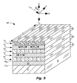
PBS10、20a、20b、30および40は、基板11の実質的な平面11Plの上に位置し得る格子層13を含む。格子層13は、細長く、実質的に平行な、交互に並んだ高屈折率領域13Hおよび低屈折率領域13Lの配列を含み得る。格子層13は、基板11の平面11Plに実質的に平行な平面13Plに位置し得る。
The
高屈折率領域13Hは、低屈折率領域13Lと異なる誘電体材料から成り得て、これら異なる材料間に明確な境界の層が存在してよい。高屈折率領域13Hは、固体の誘電体材料から成り得る。低屈折率領域13Lは、固体の誘電体材料、空気、別の気体、または真空から成り得る。細長く、実質的に平行な高屈折率領域13Hおよび低屈折率領域13Lの配列は、規則的な反復配列であってよい。
The high
低屈折率領域13Lの屈折率nLを高屈折率領域13Hの屈折率nHより十分に低くするには、誘電性PBS10、20a、20b、30および40の効率を改善することが有益であり得る。例えば、想定用途の波長範囲(例えば、可視光スペクトル)にわたって、高屈折率領域13Hの屈折率nHと、低屈折率領域13Lの屈折率nLとの間の差は、一態様において、0.3より大きく(nH − nL>0.3)、別の態様において、1.0より大きく(nH − nL>1.0)、別の態様において、1.3より大きく(nH − nL>1.3)、別の態様において、1.5より大きく(nH − nL>1.5)、または、別の態様において、1.7より大きい(nH − nL>1.7)ことがある。高い屈折率nHを有する高屈折率領域13Hの材料(例えば、可視スペクトルにおいて2.0、2.3、または、2.5より大きい)の選択により、PBS10、20a、20b、30および40の設計が改善し得る。
In order to make the refractive index n L of the low
誘電性PBS10、20a、20b、30および40の効率を改善するために、次の2つの条件(1または2)のうち1つを満たすことも有益であり得る。 1.基板11の屈折率nsubと、領域13Hおよび13Lの長さ方向Lに平行な偏光のための格子層13の実効屈折率n||との差が大きく、かつ、基板11の屈折率nsubと、領域13Hおよび13Lの長さ方向Lに鉛直な偏光のための格子層13の実効屈折率n⊥との差が小さい。例えば、格子層13および基板11は、次の方程式を満たし得る。
a.|nsub − n|||>0.3、|nsub − n|||>0.45、|nsub − n|||>0.6、|nsub − n|||>0.7、または|nsub − n|||>0.8、かつ
b.|nsub − n⊥|<0.25、|nsub − n⊥|<0.2、|nsub − n⊥|<0.15、|nsub − n⊥|<0.1、または|nsub − n⊥|<0.05。
2.基板11の屈折率nsubと、領域13Hおよび13Lの長さ方向Lに鉛直な偏光のための格子層13の実効屈折率n⊥との差が大きく、かつ、基板11の屈折率nsubと、領域13Hおよび13Lの長さ方向Lに平行な偏光のための格子層13の実効屈折率n||との差が小さい。例えば、格子層13および基板11は、次の方程式を満たし得る。
a.|nsub − n⊥|>0.3、|nsub − n⊥|>0.45、|nsub − n⊥|>0.6、|nsub − n⊥|>0.7、または|nsub − n⊥|>0.8、かつ
b.|nsub − n|||<0.25、|nsub − n|||<0.2、|nsub − n|||<0.15、|nsub − n|||<0.1、または|nsub − n|||<0.05。
上の方程式1.a、1.b、2.a、および2.bにおける所望の関係を達成するべく、デューティサイクル(WH/P)、nsub、nH、およびnLが選択され得る。
In order to improve the efficiency of the
a. | N sub -n || |> 0.3, | n sub -n || |> 0.45, | n sub -n || |> 0.6, | n sub -n || 7, or | n sub −n || |> 0.8, and b. | N sub - n ⊥ | < 0.25, | n sub - n ⊥ | <0.2, | n sub - n ⊥ | <0.15, | n sub - n ⊥ | <0.1 or, | n sub -n⊥ | <0.05.
2. The difference between the refractive index n sub of the
a. | N sub - n ⊥ |> 0.3, | n sub - n ⊥ |> 0.45, | n sub - n ⊥ |> 0.6, | n sub - n ⊥ |> 0.7 , or, | n sub -n⊥ |> 0.8, and b. | N sub −n || | <0.25, | n sub −n || | <0.2, | n sub −n || | <0.15, | n sub −n || 1, or | n sub −n || | <0.05.
Equation 1 above. a. b. a, and 2. Duty cycle (W H / P), n sub , n H , and n L can be selected to achieve the desired relationship in b.
格子層13の実効屈折率n||およびn⊥は、鉛直入射光Ln(θ=0、図4、5を参照)のための次の方程式によって概算され得る。

非鉛直入射光については、角度θはz軸に対する角度であり、角度θxzは、x − z平面(領域13Hおよび13Lに交差する平面であり、入射の平面を画定する)に対する角度である。角度θxzの非鉛直入射光Lxz(図4を参照)については、入射の平面に鉛直な偏光のための格子層13の実効屈折率n||(θxz)は、入射角θxzによって影響されない。従って、n||(θxz)=n||である。しかしながら、入射の平面に平行な偏光のための格子層13の実効屈折率n⊥(θxz)は、入射角θxzに依存する。入射角θxzである、この実効屈折率n⊥(θxz)を概算する方程式は、以下の通りである。
y − z平面(領域13Hおよび13Lに平行な平面であり、入射の平面を画定する)内の角度θyzの非鉛直入射光Lyz(図5を参照)については、入射の平面内の偏光のための格子層13の実効屈折率n||(θyz)、および、入射の平面に鉛直な偏光のための格子層13の実効屈折率n⊥(θyz)は、入射角θに影響されない。従って、n||(θyz)=n||、n⊥(θyz)=n⊥である。
For non-vertical incident light L yz (see FIG. 5) at angle θ yz in the yz plane (plane parallel to
PBS10(図1)は、基板11上に単一の格子層13のみを含み、他の層を含まない単純な誘電性PBSである。このPBSは、製造コストが低く、光の吸収量が非常に低いという利点を有し得るが、コントラストが低いという欠点を有し得る。適切に設計された薄膜層12を追加することで、効率が向上し得る(PBS20a、20b、30および40を参照)。
PBS 10 (FIG. 1) is a simple dielectric PBS that includes only a single
薄膜層12の屈折率nTFと、基板11の屈折率nsubとの間の差が小さいと、誘電性PBS20a、20b、30および40の効率が改善し得る。例えば、この差は、一態様において、0.6より低く(|nTF − nsub|<0.6)、別の態様において、0.25より低く(|nTF − nsub|<0.25)、別の態様において、0.15より低く(|nTF − nsub|<0.15)、別の態様において、0.05より低くなり得る(|nTF − nsub|<0.05)。
If the difference between the refractive index n TF of the
誘電性PBS20a、20b、30および40の効率を改善するために、次の2つの条件(3または4)のうち1つを満たすことも有益であり得る。 3.薄膜層12の屈折率nTFと、領域13Hおよび13Lの長さ方向Lに平行な偏光のための格子層13の実効屈折率n||との差が大きく、かつ、薄膜層12の屈折率nTFと、領域13Hおよび13Lの長さ方向Lに鉛直な偏光のための格子層13の実効屈折率n⊥との差が小さい。例えば、格子層13および薄膜層12は、次の方程式を満たし得る。
a.|nTF − n|||>0.3、|nTF − n|||>0.45、|nTF − n|||>0.6、|nTF − n|||>0.7、または|nTF − n|||>0.8、かつ
b.|nTF − n⊥|<0.25、|nTF − n⊥|<0.2、|nTF − n⊥|<0.15、|nTF − n⊥|<0.1、または|nTF − n⊥|<0.05。 4.薄膜層12の屈折率nTFと、領域13Hおよび13Lの長さ方向Lに鉛直な偏光のための格子層13の実効屈折率n⊥との差が大きく、かつ、薄膜層12の屈折率nTFと、領域13Hおよび13Lの長さ方向Lに平行な偏光のための格子層13の実効屈折率n||との差が小さい。例えば、格子層13および薄膜層12は、次の方程式を満たし得る。 a.|nTF −n⊥|>0.3、|nTF − n⊥|>0.45、|nTF − n⊥|>0.6、|nTF − n⊥|>0.7、または|nTF − n⊥|>0.8、かつ
b.|nTF − n|||<0.25、|nTF − n|||<0.2、|nTF − n|||<0.15、|nTF − n|||<0.1、または|nTF − n|||<0.05。
In order to improve the efficiency of the
a. | N TF −n || |> 0.3, | n TF −n || |> 0.45, | n TF −n || |> 0.6, | n TF −n || 7, or | n TF −n || |> 0.8, and b. | N TF −n⊥ | <0.25, | n TF− n⊥ | <0.2, | n TF− n⊥ | <0.15, | n TF− n⊥ | <0.1, or | n TF - n ⊥ | <0.05 . 4). The difference between the refractive index n TF of the
上の方程式3.a、3.b、4.a、および4.bにおける所望の関係を達成するべく、デューティサイクル(WH/P)、nTF、nH、およびnLが選択され得る。 Equation 3 above. a. b. a, and 4. Duty cycle (W H / P), n TF , n H , and n L can be selected to achieve the desired relationship in b.
薄膜層12は、薄膜層全体にわたり、等方性の光学特性を有し得る。薄膜層12は、y軸方向(領域13Hおよび13Lの長さ方向Lに沿う方向)およびx軸方向(領域13Hおよび13Lの長さ方向Lに鉛直な方向)において、等方性であり得る。薄膜層12は、単一材料(例えば、実質的に、二酸化ケイ素の均質層)から構成され得る。低屈折率領域13Lの材料が、高屈折率領域13Hと異なることに起因して、格子層13は、y軸方向(領域13Hおよび13Lの長さ方向Lに沿う方向)において等方性であり得るが、x軸方向(領域13Hおよび13Lの長さ方向Lに鉛直な方向)において異方性であり得る。
The
図2aに示すように、格子層13は、基板11に隣接し得て、薄膜層12と基板11との間に挟まれ得る。図2bに示すように、薄膜層12は、基板11に隣接し得て、格子層13と基板11との間に挟まれ得る。格子層13内において、高屈折率領域13Hは、低屈折率領域13Lに接触または隣接し得る。上の関係は、各誘電性PBSの設計を最適化するように選択され得る。
As shown in FIG. 2 a, the
いくつかの用途については、PBSの性能は、格子層13と薄膜層12との間に位置するグリッド層32を追加することで向上し得る(図3を参照)。グリッド層32は、細長く実質的に平行なリブ32rの配列を含み得る。各リブ32rは、示されているように、各高屈折率領域13Hと薄膜層12との間に位置し得るか、各低屈折率領域13Lと薄膜層12との間に位置し得る(図示せず)。グリッド層32は、薄膜層12と同一の材料から成り得る。グリッド層32は、薄膜層12をエッチングするためのマスクとして高屈折率領域13Hまたは低屈折率領域13Lを使用することで形成され得る。一実施形態において、グリッド層32は、10〜60ナノメートルの厚32Thを有し得る。
For some applications, the performance of the PBS may be improved by adding a
図4 − 5に示すように、格子層13および薄膜層12は共に、対43を構成し得る。PBS40は更に、一態様において、少なくとも1つの追加的な対43を含み得て、別の態様において、少なくとも2つの追加的な対43を含み得る。PBS40は、別の態様において、少なくとも1つの、15より少ない対43を含み得る。複数の対43によって、効率が向上し得る。格子層13の実効屈折率n⊥およびn||と、薄膜層12の屈折率nTFと、基板11の屈折率nsubとの間の関係における欠陥は、追加的な複数の対43によって補償され得る。より多くの対43を追加すると、コストが増加し得るので、当該の屈折率の間の関係を可能な限り最適化し、次に、必要に応じて、より多くの対43を追加することが好ましいことがある。
As shown in FIG. 4-5, both the
基板11、格子層13、グリッド層32、および/または、薄膜層12の材料は、誘電体であり得、非重合性誘電体材料であり得る。誘電体材料の例には、Na3AlF6、MgF2、ZnS、酸化チタン、SiO2、Al2O3、およびHfO2が含まれる。基板11、格子層13、グリッド層32、および/または、薄膜層12の材料が、想定用途の光スペクトルにおいて、小さい屈折率のk値部分を有することは、有益であり得る。例えば、k値は、一態様において、0.1より低く、別の態様において、0.05より低く、別の態様において、0.03より低く、別の態様において、0.01より低くてよい。k値は、想定用途のスペクトルにおける1点で、または、想定用途のスペクトル全体(例えば、400〜700ナノメートル)において、これらの値より低くてよい。
The material of the
PBS10、20a、20b、30および40の他の態様において、特定の設計の各々について性能を最適化するべく、設計は修正され得る。例えば、図1で示すように、低屈折率領域13Lの厚さ13LThは、高屈折率領域13Hの厚さ13HThと同一であり得る(従って、格子層13は、単一の厚さ13Thを有し得る)。図1で示されているように、低屈折率領域13Lの上面、および、高屈折率領域13Hの上面は、共通面13PTで終端となり得る。図1で示されているように、低屈折率領域13Lの底面、および、高屈折率領域13Hの底面は、共通面13PBで終端となり得る。図3で示されているように、低屈折率領域13Lの厚さ13LThは、高屈折率領域13Hの厚さ13HThより大きいことがあり得る。図示されていないが、低屈折率領域13Lの厚さ13LThは、高屈折率領域13Hの厚さ13HThより小さいことがあり得る。
In other aspects of
高次回折を最低限に抑えることが望ましい場合、使用される波長スペクトルにおける最低波長より小さい、または、その半分より小さいピッチPを有することが有益であり得る。例えば、可視光において使用する場合、ピッチPは、一態様において、400ナノメートルより小さいか、または、別の態様において、200ナノメートルより小さい。 If it is desirable to minimize high-order diffraction, it may be beneficial to have a pitch P that is less than or less than half the lowest wavelength in the wavelength spectrum used. For example, when used in visible light, the pitch P is less than 400 nanometers in one aspect, or less than 200 nanometers in another aspect.
高次回折を最低限に抑えるべく、低屈折率領域13Lの幅WL、および/または、高屈折率領域13Hの幅WHを、使用する波長スペクトルの最低波長より小さくするか、または、その半分より小さくすることは、有益であり得る(図4 − 5を参照)。例えば、可視光での使用については、低屈折率領域13Lの幅WL、および/または、高屈折率領域13Hの幅WHは、一態様において、400ナノメートルより小さく、別の態様において、200ナノメートルより小さく、別の態様において、100ナノメートルより小さく、別の態様において、60ナノメートルより小さくよい。
In order to suppress the high-order diffraction to a minimum, the low
格子層13および薄膜層12は、光学薄膜であり得る。例えば、格子層13は、厚13Thを有し、薄膜層12は、想定されるPBSの使用の波長範囲における光について、一態様において、1波長より小さい、または、別の態様において、1/2波長より小さい、厚さ12Thを有し得る。格子層13は、厚13Thを有し、薄膜層12は、別の態様において、400ナノメートルより小さい厚さ12Thを有し得る。
The
本明細書に記載されている誘電性PBS10、20a、20b、30および40は、ガラス製キューブ内に位置し得るので、背面焦点距離が短く、耐久性が高く、光学系への組み立てが容易であるという、プリズムの利点を有し得るが、また、MacNeilleプリズムより遥かに大きい光入射角度範囲で偏光させ得る。本明細書に記載されている誘電性PBS10、20a、20b、30、40では、他のワイヤグリッド偏光ビームスプリッタ設計と比較して、効率が向上し得る。
The
[光線分離システムおよび使用方法]
図6は、光線分離システム60を示している。光源61は、本明細書に記載された実施形態のうち1つに従って作られ得るPBS65に光62(例えば、可視光)を照射するように配置され得る。PBS65は、光62を透過ビーム64(主に一方の偏光、例えばp偏光を含み得る)と反射ビーム63(主に反対の偏光、例えばs偏光を含み得る)とに分離し得る。入射光62が、透過ビーム64および反射ビーム63の合計に等しいことが望ましい(光62=透過ビーム64+反射ビーム63)。しかしながら、吸収に起因して、入射光62は、透過ビーム64および反射ビーム63の合計より大きいことがあり得る(光62>透過ビーム64+反射ビーム63)。それ故、より大きく、より強力で、より高価な光源61が必要となり得て、冷却の必要性が増大し得て、結果的に、システム60のコスト、重量、サイズ、および騒音が増大するので、望ましくない。従って、吸収を最低限に抑えることと、入射光62が透過ビーム64および反射ビーム63の合計に等しくなるという理想の状態に近づけることとは、有益であり得る。
[Light separation system and method of use]
FIG. 6 shows a
PBS65をすべて、または、実質的にすべて、誘電体材料から作り上げることによって、吸収を最低限に抑えられ得る。従って、例えば、一態様において、PBS上の入射光62の少なくとも90%が、PBS65で反射または透過し得て(0.9×光62≦反射ビーム63+透過ビーム64)、別の態様において、PBS上の入射光62の少なくとも95%が、PBS65で反射または透過し得て、別の態様において、PBS上の入射光62の少なくとも98%が、PBS65で反射または透過し得て、別の態様において、PBS上の入射光62の少なくとも99%が、PBS65で反射または透過し得る。
By making all or substantially all of the
本明細書で記載されている、PBS10、20a、20b、30または40のうち1つを使用する方法は、次の段階を含み得る。
1.PBS10、20a、20b、30または40を光源61に配置する。
2.一態様において、入射光62の少なくとも90%を透過または反射し、別の態様において、入射光の少なくとも95を透過または反射し、別の態様において、入射光の少なくとも98を透過または反射し、別の態様において、入射光の少なくとも99%を透過または反射する。
The methods described herein using one of
1.
2. In one aspect, at least 90% of
[例示的な設計]
以下は、角度θxz=45°で空気から入射する550ナノメートル波長の光Lxzのために設計されたプレート状誘電性PBSの例示的な設計である。 1.高屈折率領域13Hは、TiO2で、nH≒2.58であり、低屈折率領域13Lは、空気で、nL≒1.0である。nH − nL=1.58。
2.薄膜層12は、MgF2で、nTF≒1.38である。
3.基板11は、Borofloat製ガラスプレートであり、nsub=1.50である。
4.ピッチは144ナノメートルである。
5.デューティサイクル(WH/P)は、65%である。
6.鉛直入射光Ln:n||=2.17、n⊥=1.50。
7.x − z平面に沿った角度45°の非鉛直入射光Lxz:n||(45°)=2.17、n⊥(45°)=1.58。
8.|nTF − n⊥|=0.20、|nsub − n⊥|=0。
9.|nTF − n|||=0.79、|nsub − n|||=0.67。
10.|nTF − nsub|=0.12。
[Example design]
The following is an exemplary design of a plate-like dielectric PBS designed for 550 nanometer wavelength light L xz incident from air at an angle θ xz = 45 °. 1. The high
2. The
3. The
4). The pitch is 144 nanometers.
5. The duty cycle (W H / P) is 65%.
6). Vertical incident light L n: n || = 2.17, n ⊥ = 1.50.
7). Non-vertical incident light L xz at an angle of 45 ° along the x-z plane: n || (45 °) = 2.17, n ⊥ (45 °) = 1.58.
8). | N TF −n ∥ | = 0.20, | n sub −n ∥ | = 0.
9. | NTF −n ||| = 0.79, | nsub −n ||| = 0.67.
10. | N TF −n sub | = 0.12.
以下は、角度θyz=45°でガラス入射する広帯域の可視光Lyzのために設計された誘電性PBSキューブの例示的な設計である。
1.高屈折率領域13Hは、TiO2で、nH≒2.58であり、低屈折率領域13Lは、スピンオングラスで、nL≒1.17である。nH − nL=1.41。
2.薄膜層12は、HfO2で、nTF≒1.93である。
3.基板11は、ガラスで、nsub≒1.88である。入射光の媒体もガラスであり、nsub≒1.88である。
4.ピッチは120ナノメートルである。
5.デューティサイクル(WH/P)は、40%である。
6.鉛直入射光Ln:n||=1.87、n⊥=1.42。
7.x − z平面に沿った角度45°の非鉛直入射光Lyz:n||(45°)=1.87、n⊥(45°)=1.42。
8.|nTF − n⊥|=0.51、|nsub − n⊥|=0.46。
9.|nTF − n|||=0.06、|nTF − n|||=0.01。
10.|nTF − nsub|=0.05。
The following is an exemplary design of a dielectric PBS cube designed for broadband visible light L yz incident on glass at an angle θ yz = 45 °.
1. The high
2. The
3. The
4). The pitch is 120 nanometers.
5. The duty cycle (W H / P) is 40%.
6). Vertical incident light L n: n || = 1.87, n ⊥ = 1.42.
7). Non-vertical incident light L yz at an angle of 45 ° along the x-z plane: n || (45 °) = 1.87, n ⊥ (45 °) = 1.42.
8). | N TF −n⊥ | = 0.51, | n sub− nn | = 0.46.
9. | N TF −n || | = 0.06, | n TF −n || | = 0.01.
10. | N TF −n sub | = 0.05.
[設計の概要]
上述の設計上の考慮事項をまとめると、光入射角度の範囲が広く、一方の偏光の透過率が高く(例えば、Tpが高い)、反対の偏光の反射が高いか制御され(例えば、Rsが高い、または、Rsが所望の値に制御されている)、効率が高く、光学系の背面焦点距離が短く、光の吸収量が少なく、および/または、光学系への組み立てが容易であるという利点を有するPBSは、以下の設計上の考慮事項によって作られ得る。
[Overview of design]
To summarize the design considerations described above, the range of light incident angles is wide, the transmittance of one polarization is high (eg, high Tp), and the reflection of the opposite polarization is high (eg, Rs is controlled). High, or Rs is controlled to the desired value), high efficiency, short back focal length of optical system, low light absorption, and / or easy assembly into optical system Advantageous PBSs can be made with the following design considerations.
第1に、ビームスプリッタは、大部分、実質的に、または全体的に、使用される波長範囲における光に対して実質的に透過的な誘電体材料(例えば、k値が低い)から作られ得る。 First, the beam splitter is made, for the most part, substantially or entirely from a dielectric material that is substantially transparent to light in the wavelength range used (eg, a low k value). obtain.
第2に、ビームスプリッタは少なくとも1つの格子層13を含み得る。格子層13は、細長く、実質的に平行で、交互に並んだ高屈折率領域13Hおよび低屈折率領域13Lの配列を含み得る。これら2つの領域13Hおよび13Lの屈折率の間の差が大きい(すなわち、nH − nLの値が大きい)と、性能が向上し得る。
Second, the beam splitter may include at least one grating
第3に、薄膜層12が使用される場合、|nTF − n⊥|が大きく、|nTF − n|||が小さくなるように、または、|nTF − n⊥|が小さく、|nTF − n|||が大きくなるように設計する。薄膜層12が使用されない場合、|nsub − n⊥|が大きく、|nsub − n|||が小さくなるように、または、|nsub − n⊥|が小さく、|nsub − n|||が大きくなるように設計する。nTF/nsubとn⊥またはn||との間の差が小さいと、一方の偏光が層の境界を通過するときの反射を最低限に抑えることが可能になる。理論上、nTF/nsub=n⊥、またはnTF=n||/nsubである場合、この偏光は、薄膜層12と格子層13との間の境界で反射しないであろう。nTF/nsubとn⊥またはn||との間の差が大きい場合、他方の偏光の反射が大きくなり得る。理論上、この差を可能な限り大きくすることは有益である。
Third, if the
第4に、|nTF − nsub|が小さくなるように設計する。これにより、基板と薄膜層12または格子層13との間のいかなる境界でも、この偏光の反射が最低限に抑えることが可能になる。理論上、nTF=nsubの場合が最適である。
Fourth, it is designed so that | n TF −n sub | This makes it possible to minimize the reflection of this polarization at any boundary between the substrate and the
実際的な設計において、材料の特性は理想的でないので、トレードオフが存在し得る。1つの設計は、主に一方の偏光の透過率について最適化し得るが、別の所望される特性を犠牲にする。別の設計は、主に一方の偏光の反射について最適化し得るが、別の所望される特性を犠牲にする。 In a practical design, tradeoffs may exist because the material properties are not ideal. One design can be optimized primarily for the transmission of one polarization, but at the expense of another desired property. Another design can be optimized primarily for reflection of one polarization, but at the expense of another desired property.
利用可能な材料の欠陥、および、製造上の欠陥に起因して、実際の設計は通常、理想的な条件を満たさない。従って、上の例示的な設計で示すように、「大きい」および「小さい」という用語は、相対的なものである。このような欠陥は、対43の数を増やすことによって、少なくとも部分的に補償され得る。しかしながら、対43の数を増やす場合、製造コストが増大し得るので、性能の向上と、偏光子のコスト増大の回避との間には、トレードオフが存在し得る。
Due to defects in available materials and manufacturing defects, actual designs usually do not meet ideal conditions. Thus, as shown in the exemplary design above, the terms “large” and “small” are relative. Such defects can be compensated at least in part by increasing the number of
[作成方法]
誘電性PBSを作成する第1の方法は、次の段階のいくつか、またはすべてを含み得る(段階1および2は、任意の順序で実施され得て、段階3は、段階1および2の後で実施され得る)。
1.次の段階aからcを順番に実施することで、格子層13を形成する。
a.基板11の上に平行な第1領域13R1の配列を形成する。例えば、材料13M1を基板11上にスパッタリングし(図7を参照)、次に、材料13M1をパターニングおよびエッチングして、第1領域13R1を形成する(図8を参照)。グリッド層32を作成することが望ましい場合、下の材料(例えば、薄膜層12または基板11)にエッチングするべく、マスクとして、第1領域13R1が使用され得る。
b.第1領域13R1の間の細長い溝83、および、第1領域13R1の上を、第2材料13M2(例えば、スピンオンまたはALD)で満たす。図8 − 9を参照。
c.第1領域13R1の上部13R1Tが第2材料13M2を実質的に含まないように、第2材料13M2をエッチングして、溝83内に第2領域13R2を形成する。図9 − 10を参照。
2.基板11の表面上に薄膜層12を(例えば、スパッタリングによって)形成する。図11を参照。
3.段階1 − 2を繰り返す(この段階3は複数回繰り返される)。
第1領域13R1または第2領域13R2のいずれかは、高屈折率領域13Hであり得て、第1領域13R1または第2領域13R2の他方は、低屈折率領域13Lであり得る。
[How to make]
The first method of making a dielectric PBS can include some or all of the following steps (steps 1 and 2 can be performed in any order, and step 3 follows steps 1 and 2 Can be implemented).
1. The lattice layers 13 are formed by sequentially performing the following steps a to c.
a. An array of parallel
b. The
c. As the top 13 R1T the first region 13 R1 does not include the second material 13 M2 substantially, by etching the second material 13 M2, to form the second region 13 R2 in the
2. A
3. Repeat steps 1-2 (this step 3 is repeated multiple times).
Either the
誘電性PBSを作成する第2の方法は、次の段階のいくつか、またはすべてを含み得る(段階1および2は、任意の順序で実施され得て、段階3は、段階1および2の後で実施され得る)。
1.基板11の表面上に薄膜層12を(例えば、スパッタリングによって)形成する。図12を参照。
2.平行で細長い高屈折率領域13Hの配列を基板11の表面上に形成することで、格子層13を形成する。例えば、高屈折率領域13Hの材料を基板11上にスパッタリングし、次に、パターニングおよびエッチングを実施して、高屈折率領域13Hを形成する。図3に示すように、グリッド層32を作成することが望ましい場合、薄膜層12にエッチングするべく、マスクとして、高屈折率領域13Hが使用され得る。高屈折率領域13Hの間の、空気で満たされた溝は、低屈折率領域13Lであり得る。図13を参照。
3.段階1 − 2を繰り返す(段階3は複数回繰り返され得る)。図14を参照。低屈折率領域13Lを薄膜層の材料で満たすことなく、格子層13の上に薄膜層12を堆積させることは困難であり得る。薄膜層12の材料で低屈折率領域13Lが満たされることを最低限に抑えるべく、大きな斜角(例えば80°)での堆積、または、参照によって本明細書に組み込まれる米国特許出願第2012/0075699号に記載される方法が使用され得る。
A second method of making a dielectric PBS may include some or all of the following steps (steps 1 and 2 can be performed in any order, and step 3 follows steps 1 and 2 Can be implemented).
1. A
2. The
3. Repeat steps 1-2 (step 3 can be repeated multiple times). See FIG. It may be difficult to deposit the
Claims (20)
a.実質的な平面を有する基板を備え、
b.前記基板の前記平面上に配置される格子層および薄膜層を備え、
c.前記格子層は、細長く実質的に平行な、交互に並んだ複数の高屈折率領域と複数の低屈折率領域との配列を含み、
d.前記格子層は、前記基板の前記平面に実質的に平行な平面内に配置され、
e.前記複数の低屈折率領域の屈折率(nL)は、前記複数の高屈折率領域の屈折率(nH)より低く、
f.前記格子層および前記薄膜層は、
i.|nTF − n|||>0.7および|nTF − n⊥|<0.25、または、
ii.|nTF − n⊥|>0.7および|nTF − n|||<0.25、
の方程式を満たし、
iii.ここで、
1.nTFは、前記薄膜層の屈折率であり、
2.n||は、前記複数の高屈折率領域および前記複数の低屈折率領域の長さ方向に平行な偏光のための前記格子層の実効屈折率であり、
3.n⊥は、前記複数の高屈折率領域および前記複数の低屈折率領域の長さ方向に鉛直な偏光のための前記格子層の実効屈折率であり、
4.nTFは、前記薄膜層の屈折率であり、
g.前記格子層の材料は誘電体であり、前記薄膜層の材料は誘電体である、
誘電体偏光ビームスプリッタ(PBS)。 A dielectric polarization beam splitter (PBS),
a. Comprising a substrate having a substantially planar surface;
b. Comprising a lattice layer and a thin film layer disposed on the plane of the substrate;
c. The lattice layer includes an array of a plurality of alternating high refractive index regions and a plurality of low refractive index regions that are elongated and substantially parallel.
d. The lattice layer is disposed in a plane substantially parallel to the plane of the substrate;
e. The refractive index (n L ) of the plurality of low refractive index regions is lower than the refractive index (n H ) of the plurality of high refractive index regions,
f. The lattice layer and the thin film layer are:
i. | N TF −n || |> 0.7 and | n TF −n⊥ | <0.25, or
ii. | N TF −n⊥ |> 0.7 and | n TF −n || | <0.25,
Satisfy the equation
iii. here,
1. n TF is the refractive index of the thin film layer,
2. n || is the effective refractive index of the grating layer for polarized light parallel to the length direction of the plurality of high refractive index regions and the plurality of low refractive index regions;
3. n ⊥ is the effective refractive index of the grating layer for polarized light perpendicular to the length direction of the plurality of high refractive index regions and the plurality of low refractive index regions,
4). n TF is the refractive index of the thin film layer,
g. The material of the lattice layer is a dielectric, and the material of the thin film layer is a dielectric.
Dielectric polarization beam splitter (PBS).
a.実質的な平面を有する基板を備え、
b.前記基板の前記平面上に配置された格子層および薄膜層を備え、
c.前記格子層は、細長く実質的に平行な、交互に並んだ複数の高屈折率領域と複数の低屈折率領域との配列を含み、
d.前記格子層は、前記基板の前記平面に実質的に平行な平面内に配置され、
e.前記複数の低屈折率領域の屈折率(nL)は、前記複数の高屈折率領域の屈折率(nH)より低く、
f.前記格子層および前記薄膜層は、
i.|nTF − n|||>0.45および|nTF − n⊥|<0.1、または、
ii.|nTF − n⊥|>0.45および|nTF − n|||<0.1、
の方程式を満たし、
iii.ここで、
1.nTFは、前記薄膜層の屈折率であり、
2.n||は、前記複数の高屈折率領域および前記複数の低屈折率領域の長さ方向に平行な偏光のための前記格子層の実効屈折率であり、
3.n⊥は、前記複数の高屈折率領域および前記複数の低屈折率領域の長さ方向に鉛直な偏光のための前記格子層の実効屈折率であり、
4.nTFは、前記薄膜層の屈折率であり、
g.前記格子層および前記薄膜層の複数の材料は、屈折率のk値部分が0.05より小さい誘電体材料である、
誘電体偏光ビームスプリッタ(PBS)。 A dielectric polarization beam splitter (PBS),
a. Comprising a substrate having a substantially planar surface;
b. Comprising a lattice layer and a thin film layer disposed on the plane of the substrate;
c. The lattice layer includes an array of a plurality of alternating high refractive index regions and a plurality of low refractive index regions that are elongated and substantially parallel.
d. The lattice layer is disposed in a plane substantially parallel to the plane of the substrate;
e. The refractive index (n L ) of the plurality of low refractive index regions is lower than the refractive index (n H ) of the plurality of high refractive index regions,
f. The lattice layer and the thin film layer are:
i. | N TF −n || |> 0.45 and | n TF −n⊥ | <0.1, or
ii. | N TF −n⊥ |> 0.45 and | n TF −n || | <0.1,
Satisfy the equation
iii. here,
1. n TF is the refractive index of the thin film layer,
2. n || is the effective refractive index of the grating layer for polarized light parallel to the length direction of the plurality of high refractive index regions and the plurality of low refractive index regions;
3. n ⊥ is the effective refractive index of the grating layer for polarized light perpendicular to the length direction of the plurality of high refractive index regions and the plurality of low refractive index regions,
4). n TF is the refractive index of the thin film layer,
g. The plurality of materials of the lattice layer and the thin film layer are dielectric materials in which the k value portion of the refractive index is smaller than 0.05.
Dielectric polarization beam splitter (PBS).
a.実質的な平面を有する基板を備え、
b.前記基板の前記平面上に配置される格子層および薄膜層を備え、
c.前記格子層は、細長く実質的に平行な、交互に並んだ複数の高屈折率領域と複数の低屈折率領域との配列を含み、
d.前記格子層は、前記基板の前記平面に実質的に平行な平面内に配置され、
e.前記複数の低屈折率領域の屈折率(nL)は、前記複数の高屈折率領域の屈折率(nH)より低く、
f.前記格子層の材料は誘電体であり、前記薄膜層の材料は誘電体である、
誘電体偏光ビームスプリッタ(PBS)。 A dielectric polarization beam splitter (PBS),
a. Comprising a substrate having a substantially planar surface;
b. Comprising a lattice layer and a thin film layer disposed on the plane of the substrate;
c. The lattice layer includes an array of a plurality of alternating high refractive index regions and a plurality of low refractive index regions that are elongated and substantially parallel.
d. The lattice layer is disposed in a plane substantially parallel to the plane of the substrate;
e. The refractive index (n L ) of the plurality of low refractive index regions is lower than the refractive index (n H ) of the plurality of high refractive index regions,
f. The material of the lattice layer is a dielectric, and the material of the thin film layer is a dielectric.
Dielectric polarization beam splitter (PBS).
5. The refractive index (n L ) of the plurality of low refractive index regions and the refractive index (n H ) of the plurality of high refractive index regions satisfy an equation of n H −n L > 1.5. PBS.
a.|nTF − n|||>0.7および|nTF − n⊥|<0.25、または、
b.|nTF − n⊥|>0.7および|nTF − n|||<0.25
の方程式を満たし、
c.ここで、
i.鉛直入射光について、
iv.WLは、前記複数の低屈折率領域の幅であり、
v.WHは、前記複数の高屈折率領域の幅であり、
vi.Pは、前記複数の高屈折率領域のピッチである、
請求項4に記載のPBS。 The lattice layer and the thin film layer are:
a. | N TF −n || |> 0.7 and | n TF −n⊥ | <0.25, or
b. | N TF −n⊥ |> 0.7 and | n TF −n || | <0.25
Satisfy the equation
c. here,
i. For vertically incident light
iv. W L is the width of the plurality of low refractive index regions,
v. W H is the width of the plurality of high refractive index regions,
vi. P is the pitch of the plurality of high refractive index regions,
The PBS according to claim 4.
a.|nTF − n|||>0.45および|nTF − n⊥|<0.1、または、
b.|nTF − n⊥|>0.45および|nTF − n|||<0.1
の方程式を満たし、
c.ここで、
i.鉛直入射光について、
iv.WLは、前記複数の低屈折率領域の幅であり、
v.WHは、前記複数の高屈折率領域の幅であり、
vi.Pは、前記複数の高屈折率領域のピッチである、
請求項4に記載のPBS。 The lattice layer and the thin film layer are:
a. | N TF −n || |> 0.45 and | n TF −n⊥ | <0.1, or
b. | N TF −n⊥ |> 0.45 and | n TF −n || | <0.1
Satisfy the equation
c. here,
i. For vertically incident light
iv. W L is the width of the plurality of low refractive index regions,
v. W H is the width of the plurality of high refractive index regions,
vi. P is the pitch of the plurality of high refractive index regions,
The PBS according to claim 4.
a.|nTF − n|||>0.7および|nTF − n⊥|<0.25、または、
b.|nTF − n⊥|>0.7および|nTF − n|||<0.25
の方程式を満たし、
c.ここで、
i.nTFは、前記薄膜層の屈折率であり、
ii.n||は、前記複数の高屈折率領域および前記複数の低屈折率領域の長さ方向に平行な偏光のための前記格子層の実効屈折率であり、
iii.n⊥は、前記複数の高屈折率領域および前記複数の低屈折率領域の長さ方向に鉛直な偏光のための前記格子層の実効屈折率であり、
iv.nTFは、前記薄膜層の屈折率である、
請求項4に記載のPBS。 The lattice layer and the thin film layer are:
a. | N TF −n || |> 0.7 and | n TF −n⊥ | <0.25, or
b. | N TF −n⊥ |> 0.7 and | n TF −n || | <0.25
Satisfy the equation
c. here,
i. n TF is the refractive index of the thin film layer,
ii. n || is the effective refractive index of the grating layer for polarized light parallel to the length direction of the plurality of high refractive index regions and the plurality of low refractive index regions;
iii. n ⊥ is the effective refractive index of the grating layer for polarized light perpendicular to the length direction of the plurality of high refractive index regions and the plurality of low refractive index regions,
iv. n TF is the refractive index of the thin film layer,
The PBS according to claim 4.
a.|nTF − n|||>0.45および|nTF − n⊥|<0.1、または、
b.|nTF − n⊥|>0.45および|nTF − n|||<0.1、
の方程式を満たし、
c.ここで、
i.nTFは、前記薄膜層の屈折率であり、
ii.n||は、前記複数の高屈折率領域および前記複数の低屈折率領域の長さ方向に平行な偏光のための格子層の実効屈折率であり、
iii.n⊥は、前記複数の高屈折率領域および前記複数の低屈折率領域の長さ方向に鉛直な偏光のための前記格子層の実効屈折率であり、
iv.nTFは、前記薄膜層の屈折率である、
請求項4に記載のPBS。 The lattice layer and the thin film layer are
a. | N TF −n || |> 0.45 and | n TF −n⊥ | <0.1, or
b. | N TF −n⊥ |> 0.45 and | n TF −n || | <0.1,
Satisfy the equation
c. here,
i. n TF is the refractive index of the thin film layer,
ii. n || is the effective refractive index of the grating layer for polarized light parallel to the length direction of the plurality of high refractive index regions and the plurality of low refractive index regions,
iii. n ⊥ is the effective refractive index of the grating layer for polarized light perpendicular to the length direction of the plurality of high refractive index regions and the plurality of low refractive index regions,
iv. n TF is the refractive index of the thin film layer,
The PBS according to claim 4.
a.nTFは、前記薄膜層の屈折率であり、
b.nsubは、前記基板の屈折率である、
請求項4に記載のPBS。 The thin film layer and the substrate satisfy the equation | n TF −n sub | <0.15;
a. n TF is the refractive index of the thin film layer,
b. n sub is the refractive index of the substrate,
The PBS according to claim 4.
請求項4に記載のPBS。 The plurality of materials of the substrate, the lattice layer, and the thin film layer are dielectric materials in which the k value portion of the refractive index is smaller than 0.03.
The PBS according to claim 4.
b.前記PBSは更に、少なくとも2つの追加的な対を備える、請求項4に記載のPBS。 a. The lattice layer and the thin film layer together constitute a pair,
b. The PBS of claim 4, wherein the PBS further comprises at least two additional pairs.
b.前記PBSは、少なくとも1つの、15より少ない対を含む、
請求項4に記載のPBS。 a. The lattice layer and the thin film layer constitute a pair,
b. The PBS comprises at least one, fewer than 15 pairs;
The PBS according to claim 4.
a.格子層が、基板の実質的な平面上に配置され、
b.前記格子層は、細長く実質的に平行な、交互に並んだ複数の高屈折率領域と複数の低屈折率領域との配列を含み、
c.前記格子層は、前記基板の前記平面に実質的に平行な平面に配置され、
d.前記複数の低屈折率領域の屈折率(nL)および前記複数の高屈折率領域の屈折率(nH)は、400〜700ナノメートルの範囲で、nH − nL>1.3の方程式を満たし、
e.前記格子層の材料は誘電体である、
可視スペクトルのための偏光ビームスプリッタ(PBS)。 A polarizing beam splitter (PBS) for the visible spectrum,
a. A lattice layer is disposed on a substantial plane of the substrate;
b. The lattice layer includes an array of a plurality of alternating high refractive index regions and a plurality of low refractive index regions that are elongated and substantially parallel.
c. The lattice layer is disposed in a plane substantially parallel to the plane of the substrate;
d. The refractive index (n L ) of the plurality of low refractive index regions and the refractive index (n H ) of the plurality of high refractive index regions are in the range of 400 to 700 nanometers, and n H −n L > 1.3. Satisfy the equation,
e. The material of the lattice layer is a dielectric,
Polarizing beam splitter (PBS) for the visible spectrum.
b.入射する可視光の少なくとも95%を透過または反射する、
請求項17に記載の前記PBSの使用方法。 a. Place the PBS in a visible light source,
b. Transmit or reflect at least 95% of incident visible light;
The method of using the PBS according to claim 17.
b.前記複数の低屈折率領域の底面および前記複数の高屈折率領域の底面は、共通面において終端となる、
請求項17に記載のPBS。 a. The upper surfaces of the plurality of low refractive index regions and the upper surfaces of the plurality of high refractive index regions are terminated at a common surface,
b. The bottom surfaces of the plurality of low refractive index regions and the bottom surfaces of the plurality of high refractive index regions are terminated at a common plane.
The PBS of claim 17.
Applications Claiming Priority (7)
| Application Number | Priority Date | Filing Date | Title |
|---|---|---|---|
| US201462069649P | 2014-10-28 | 2014-10-28 | |
| US62/069,649 | 2014-10-28 | ||
| US201462097476P | 2014-12-29 | 2014-12-29 | |
| US62/097,476 | 2014-12-29 | ||
| US14/841,234 | 2015-08-31 | ||
| US14/841,234 US20160116754A1 (en) | 2014-10-28 | 2015-08-31 | Dielectric Polarizing Beam Splitter |
| PCT/US2015/047952 WO2016069103A1 (en) | 2014-10-28 | 2015-09-01 | Dielectric polarizing beam splitter |
Publications (1)
| Publication Number | Publication Date |
|---|---|
| JP2017533451A true JP2017533451A (en) | 2017-11-09 |
Family
ID=55791876
Family Applications (1)
| Application Number | Title | Priority Date | Filing Date |
|---|---|---|---|
| JP2017511936A Pending JP2017533451A (en) | 2014-10-28 | 2015-09-01 | Dielectric polarization beam splitter |
Country Status (4)
| Country | Link |
|---|---|
| US (1) | US20160116754A1 (en) |
| JP (1) | JP2017533451A (en) |
| KR (1) | KR20170073598A (en) |
| WO (1) | WO2016069103A1 (en) |
Families Citing this family (3)
| Publication number | Priority date | Publication date | Assignee | Title |
|---|---|---|---|---|
| US10234613B2 (en) | 2015-02-06 | 2019-03-19 | Moxtek, Inc. | High contrast inverse polarizer |
| US10139536B2 (en) * | 2016-11-22 | 2018-11-27 | Moxtek, Inc. | Embedded wire grid polarizer with high reflectivity on both sides |
| CN109557606A (en) * | 2017-09-25 | 2019-04-02 | 佳能株式会社 | Polarization beam apparatus and image projection device |
Family Cites Families (7)
| Publication number | Priority date | Publication date | Assignee | Title |
|---|---|---|---|---|
| US6447120B2 (en) * | 1999-07-28 | 2002-09-10 | Moxtex | Image projection system with a polarizing beam splitter |
| JP4593894B2 (en) * | 2003-09-01 | 2010-12-08 | キヤノン株式会社 | Optical encoder |
| JP2006133403A (en) * | 2004-11-04 | 2006-05-25 | Canon Inc | Polarized beam splitter |
| US20080055719A1 (en) * | 2006-08-31 | 2008-03-06 | Perkins Raymond T | Inorganic, Dielectric Grid Polarizer |
| US7524073B2 (en) * | 2006-11-16 | 2009-04-28 | Canon Kabushiki Kaisha | Layered periodic structures with peripheral supports |
| JP2010261999A (en) * | 2009-04-30 | 2010-11-18 | Ricoh Co Ltd | Optical element, polarizing filter, optical isolator, and optical device |
| KR101321079B1 (en) * | 2012-02-28 | 2013-10-23 | 광운대학교 산학협력단 | Wavelength filter based on a subwavelength metal grating |
-
2015
- 2015-08-31 US US14/841,234 patent/US20160116754A1/en not_active Abandoned
- 2015-09-01 KR KR1020177010021A patent/KR20170073598A/en unknown
- 2015-09-01 JP JP2017511936A patent/JP2017533451A/en active Pending
- 2015-09-01 WO PCT/US2015/047952 patent/WO2016069103A1/en active Application Filing
Also Published As
| Publication number | Publication date |
|---|---|
| US20160116754A1 (en) | 2016-04-28 |
| KR20170073598A (en) | 2017-06-28 |
| WO2016069103A1 (en) | 2016-05-06 |
Similar Documents
| Publication | Publication Date | Title |
|---|---|---|
| JP7187745B2 (en) | Wire grid polarizer with high reflectivity on both sides | |
| JP4843617B2 (en) | Multilayer wire grid polarizer | |
| JP7125640B2 (en) | Manufacturing method of transmission type diffraction grating | |
| EP1510838B1 (en) | Polarization beam splitter, optical system and image displaying apparatus using the same | |
| US6665119B1 (en) | Wire grid polarizer | |
| US9910198B2 (en) | Optical filter and optical apparatus | |
| JP2005534981A (en) | Precision phase lag device and method of manufacturing the same | |
| US20170184898A1 (en) | Wire Grid Polarizer with Dual Absorptive Regions | |
| JP2002328234A (en) | Wire grid polarizer | |
| CN107179576B (en) | A kind of gradual change phase metal grating of visible light wave range | |
| JP2004280050A5 (en) | ||
| CN111913246B (en) | Polarizing plate, optical device, and method for manufacturing polarizing plate | |
| JP2017533451A (en) | Dielectric polarization beam splitter | |
| JP4427026B2 (en) | Polarizer and polarization separation element | |
| JP6611443B2 (en) | Optical filter and optical device | |
| US20150022893A1 (en) | Diffraction Grating and Method for the Production Thereof | |
| JP2001083321A (en) | Polarizer and method for its production | |
| JP6999719B2 (en) | Polarizing elements and LCD projectors | |
| US20240069378A1 (en) | Optical device | |
| RU81601U1 (en) | RESONANT GRILLE WAVEGUIDE MIRROR | |
| US8809890B2 (en) | Reflective phase retarder and semiconductor light-emitting device including such reflecting phase retarder | |
| CN109665722B (en) | High-transparency composite glass | |
| WO2021230275A1 (en) | Polarization plate, production method therefor, and optical instrument | |
| JP6378252B2 (en) | Polarizing element and liquid crystal projector | |
| JP2012247455A (en) | Polarization separation element |