JP2017531865A - イベントベースのコンピュータビジョン計算 - Google Patents
イベントベースのコンピュータビジョン計算 Download PDFInfo
- Publication number
- JP2017531865A JP2017531865A JP2017516855A JP2017516855A JP2017531865A JP 2017531865 A JP2017531865 A JP 2017531865A JP 2017516855 A JP2017516855 A JP 2017516855A JP 2017516855 A JP2017516855 A JP 2017516855A JP 2017531865 A JP2017531865 A JP 2017531865A
- Authority
- JP
- Japan
- Prior art keywords
- sensor
- sensor element
- dedicated
- event
- feature
- Prior art date
- Legal status (The legal status is an assumption and is not a legal conclusion. Google has not performed a legal analysis and makes no representation as to the accuracy of the status listed.)
- Pending
Links
- 238000004364 calculation method Methods 0.000 title claims abstract description 31
- 238000000034 method Methods 0.000 claims abstract description 64
- 230000008859 change Effects 0.000 claims abstract description 37
- 230000000007 visual effect Effects 0.000 claims description 26
- 230000002093 peripheral effect Effects 0.000 claims description 21
- 238000001514 detection method Methods 0.000 abstract description 50
- 230000008569 process Effects 0.000 description 20
- 238000004891 communication Methods 0.000 description 12
- 238000010586 diagram Methods 0.000 description 11
- 230000015654 memory Effects 0.000 description 10
- 230000003936 working memory Effects 0.000 description 10
- 235000019580 granularity Nutrition 0.000 description 8
- 230000003287 optical effect Effects 0.000 description 5
- 230000005540 biological transmission Effects 0.000 description 4
- 239000003990 capacitor Substances 0.000 description 4
- 238000012986 modification Methods 0.000 description 4
- 230000004048 modification Effects 0.000 description 4
- ORQBXQOJMQIAOY-UHFFFAOYSA-N nobelium Chemical compound [No] ORQBXQOJMQIAOY-UHFFFAOYSA-N 0.000 description 3
- 230000007613 environmental effect Effects 0.000 description 2
- 230000006870 function Effects 0.000 description 2
- 238000009434 installation Methods 0.000 description 2
- 239000003550 marker Substances 0.000 description 2
- 230000004044 response Effects 0.000 description 2
- RYGMFSIKBFXOCR-UHFFFAOYSA-N Copper Chemical compound [Cu] RYGMFSIKBFXOCR-UHFFFAOYSA-N 0.000 description 1
- 230000001133 acceleration Effects 0.000 description 1
- 230000010267 cellular communication Effects 0.000 description 1
- 230000006835 compression Effects 0.000 description 1
- 238000007906 compression Methods 0.000 description 1
- 238000004590 computer program Methods 0.000 description 1
- 238000010276 construction Methods 0.000 description 1
- 238000013500 data storage Methods 0.000 description 1
- 230000006837 decompression Effects 0.000 description 1
- 238000005516 engineering process Methods 0.000 description 1
- 230000017525 heat dissipation Effects 0.000 description 1
- 238000007726 management method Methods 0.000 description 1
- 239000013307 optical fiber Substances 0.000 description 1
- 239000007787 solid Substances 0.000 description 1
- 230000003068 static effect Effects 0.000 description 1
- 239000000126 substance Substances 0.000 description 1
- 230000009466 transformation Effects 0.000 description 1
- 230000001052 transient effect Effects 0.000 description 1
- 230000001960 triggered effect Effects 0.000 description 1
Images


Classifications
-
- G—PHYSICS
- G06—COMPUTING; CALCULATING OR COUNTING
- G06F—ELECTRIC DIGITAL DATA PROCESSING
- G06F3/00—Input arrangements for transferring data to be processed into a form capable of being handled by the computer; Output arrangements for transferring data from processing unit to output unit, e.g. interface arrangements
- G06F3/01—Input arrangements or combined input and output arrangements for interaction between user and computer
- G06F3/03—Arrangements for converting the position or the displacement of a member into a coded form
- G06F3/041—Digitisers, e.g. for touch screens or touch pads, characterised by the transducing means
- G06F3/042—Digitisers, e.g. for touch screens or touch pads, characterised by the transducing means by opto-electronic means
- G06F3/0425—Digitisers, e.g. for touch screens or touch pads, characterised by the transducing means by opto-electronic means using a single imaging device like a video camera for tracking the absolute position of a single or a plurality of objects with respect to an imaged reference surface, e.g. video camera imaging a display or a projection screen, a table or a wall surface, on which a computer generated image is displayed or projected
-
- G—PHYSICS
- G06—COMPUTING; CALCULATING OR COUNTING
- G06V—IMAGE OR VIDEO RECOGNITION OR UNDERSTANDING
- G06V10/00—Arrangements for image or video recognition or understanding
- G06V10/40—Extraction of image or video features
- G06V10/44—Local feature extraction by analysis of parts of the pattern, e.g. by detecting edges, contours, loops, corners, strokes or intersections; Connectivity analysis, e.g. of connected components
-
- G—PHYSICS
- G06—COMPUTING; CALCULATING OR COUNTING
- G06V—IMAGE OR VIDEO RECOGNITION OR UNDERSTANDING
- G06V10/00—Arrangements for image or video recognition or understanding
- G06V10/94—Hardware or software architectures specially adapted for image or video understanding
- G06V10/955—Hardware or software architectures specially adapted for image or video understanding using specific electronic processors
-
- H—ELECTRICITY
- H01—ELECTRIC ELEMENTS
- H01L—SEMICONDUCTOR DEVICES NOT COVERED BY CLASS H10
- H01L27/00—Devices consisting of a plurality of semiconductor or other solid-state components formed in or on a common substrate
- H01L27/14—Devices consisting of a plurality of semiconductor or other solid-state components formed in or on a common substrate including semiconductor components sensitive to infrared radiation, light, electromagnetic radiation of shorter wavelength or corpuscular radiation and specially adapted either for the conversion of the energy of such radiation into electrical energy or for the control of electrical energy by such radiation
- H01L27/144—Devices controlled by radiation
- H01L27/146—Imager structures
- H01L27/14643—Photodiode arrays; MOS imagers
-
- H—ELECTRICITY
- H04—ELECTRIC COMMUNICATION TECHNIQUE
- H04N—PICTORIAL COMMUNICATION, e.g. TELEVISION
- H04N25/00—Circuitry of solid-state image sensors [SSIS]; Control thereof
- H04N25/70—SSIS architectures; Circuits associated therewith
- H04N25/71—Charge-coupled device [CCD] sensors; Charge-transfer registers specially adapted for CCD sensors
- H04N25/75—Circuitry for providing, modifying or processing image signals from the pixel array
-
- H—ELECTRICITY
- H04—ELECTRIC COMMUNICATION TECHNIQUE
- H04N—PICTORIAL COMMUNICATION, e.g. TELEVISION
- H04N25/00—Circuitry of solid-state image sensors [SSIS]; Control thereof
- H04N25/70—SSIS architectures; Circuits associated therewith
- H04N25/76—Addressed sensors, e.g. MOS or CMOS sensors
- H04N25/77—Pixel circuitry, e.g. memories, A/D converters, pixel amplifiers, shared circuits or shared components
-
- G—PHYSICS
- G06—COMPUTING; CALCULATING OR COUNTING
- G06V—IMAGE OR VIDEO RECOGNITION OR UNDERSTANDING
- G06V10/00—Arrangements for image or video recognition or understanding
- G06V10/40—Extraction of image or video features
- G06V10/46—Descriptors for shape, contour or point-related descriptors, e.g. scale invariant feature transform [SIFT] or bags of words [BoW]; Salient regional features
- G06V10/467—Encoded features or binary features, e.g. local binary patterns [LBP]
Abstract
Description
いくつかの例示的な実施形態について、本明細書の一部を形成する添付図面に関して説明する。本開示の1つまたは複数の態様が実装され得る特定の実施形態について以下で説明するが、本開示の範囲または添付の特許請求の範囲の趣旨から逸脱することなく、他の実施形態が使用されることがあり、様々な修正が行われることがある。
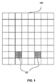
102 センサ素子
200 ピクセル
202 センサ素子
204 ピクセル内回路
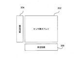
302 センサ素子アレイ
304 周辺回路
306 周辺回路
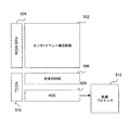
402 センサ素子アレイ
404 専用CV処理モジュール
406 アプリケーションプロセッサ
506 列並列SRAM
508 アナログ-デジタル変換器
512 プロセッサ、画像プロセッサ
602 フォトダイオード、センサ素子
604 動的視覚センサ(DVS)、イベント検出モジュール
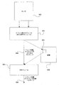
702 センサ
704 イベント検出モジュール
706 CVモジュール
900 センサ素子アレイ
901 DVSモジュール
902 画像ピクセル値のグループ
903 CVモジュール
904 画像
906 情報
908 オプションの特徴ペイロード
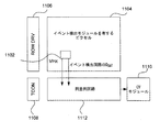
1002 センサ回路
1004 DVSおよび/またはCV回路、CVブロック
1102 ピクセル
1110 CVモジュール
1112 列並列SRAM
1202 ピクセル
1206 行ドライバ
1208 タイミングコントローラ
1210 CVモジュール
1212 列並列インベント検出モジュール
1214 アービタ回路
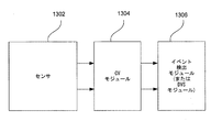
1302 センサ
1304 CVモジュール
1306 DVSモジュール
1502 ピクセル
1504 センサ回路
1506 CV回路
1508 SRAM、SRAMセル
1510 比較器
1702 センサ装置
1706 CVモジュール
1708 SRAM
1710 比較器
1802 センサ装置
1804 センサ回路
1806 CVモジュール
1808 SRAM
1810 比較器
1900 コンピューティングデバイス
1905 バス
1910 プロセッサ
1915 入力デバイス
1920 出力デバイス
1925 非一時的記憶デバイス
1930 通信サブシステム
1935 作業メモリ
1940 オペレーティングシステム
1945 アプリケーションプログラム
1950 カメラセンサ、センサ
Claims (30)
- センサ読取り値に基づいて計算結果を生成するための方法であって、
対象センサ素子に入射する光に基づく少なくとも1つのセンサ読取り値を受信するステップであって、前記対象センサ素子が、複数のセンサ素子を備えるセンサ素子アレイからのものであり、前記複数のセンサ素子が、前記センサ素子アレイの少なくとも第1の寸法および第2の寸法に沿って配置された、ステップと、
前記対象センサ素子および前記対象センサ素子に対する隣接センサ素子に関する少なくとも1つのセンサ読取り値に基づいて、専用コンピュータビジョン(CV)計算ハードウェアを使用して局所CV特徴を計算するステップと、
前記対象センサ素子に関する以前に計算されたCV特徴からの前記計算されたCV特徴における変化に基づいてイベントを生成するステップであって、前記イベントが、前記計算されたCV特徴における前記変化に関連する前記対象センサ素子の位置に関する情報を含む、ステップと
を備える方法。 - 前記専用CV計算ハードウェアが、専用CV処理モジュールとして実装される、請求項1に記載の方法。
- 前記専用CV計算ハードウェアが、ピクセル内回路または周辺回路の一部として実装される、請求項1に記載の方法。
- ピクセルが、前記センサ素子とピクセル内回路とを備える、請求項1に記載の方法。
- 前記専用CV計算ハードウェアにおいて生成された前記イベントが、アプリケーションプロセッサに送られる、請求項1に記載の方法。
- 前記局所CV特徴を計算するステップが、局所バイナリパターン(LBP)ラベルまたは前記LBPラベルの変形を生成するステップを備える、請求項1に記載の方法。
- 前記局所CV特徴を計算するステップが、符号付き勾配(HSG)ラベルのヒストグラムを生成するステップを備える、請求項1に記載の方法。
- 前記センサ素子アレイが、視覚センサであり、前記センサ素子アレイの前記複数のセンサ素子の各々が、少なくとも1つのフォトダイオードを備える、請求項1に記載の方法。
- 前記イベントが、動的視覚センサ(DVS)回路を使用して生成される、請求項1に記載の方法。
- 複数のセンサ素子を備えるセンサ素子アレイであって、前記複数のセンサ素子が、前記センサ素子アレイの少なくとも第1の寸法および第2の寸法に沿って配置され、前記複数のセンサ素子の各々が、前記センサ素子に入射する光に基づいてセンサ読取り値を生成することが可能である、センサ素子アレイと、
対象センサ素子および前記対象センサ素子に対する隣接センサ素子に関する少なくともセンサ読取り値に基づいて前記対象センサ素子に関する局所コンピュータビジョン(CV)特徴を計算し、
前記対象センサ素子に関する以前に計算されたCV特徴からの前記計算されたCV特徴における変化に基づいてイベントを生成するように構成され、前記イベントが、前記計算されたCV特徴における前記変化に関連する前記対象センサ素子の位置に関する情報を含む、専用CV計算ハードウェアと
を備える視覚センサ。 - 前記専用CV計算ハードウェアが、専用CV処理モジュールとして実装された、請求項10に記載の視覚センサ。
- 前記専用CV計算ハードウェアが、ピクセル内回路または周辺回路の一部として実装された、請求項10に記載の視覚センサ。
- ピクセルが、前記センサ素子と前記ピクセル内回路とを備える、請求項12に記載の視覚センサ。
- 前記専用CV計算ハードウェアにおいて生成された前記イベントが、アプリケーションプロセッサに送られる、請求項10に記載の視覚センサ。
- 前記局所CV特徴を計算することが、局所バイナリパターン(LBP)ラベルまたは前記LBPラベルの変形を生成することを備える、請求項10に記載の視覚センサ。
- 前記局所コンピュータCV特徴を計算することが、符号付き勾配(HSG)ラベルのヒストグラムを生成することを備える、請求項10に記載の視覚センサ。
- 前記センサ素子アレイの前記センサ素子の各々が、少なくとも1つのフォトダイオードを備える、請求項10に記載の視覚センサ。
- 前記イベントが、動的視覚センサ(DVS)回路を使用して生成される、請求項10に記載の視覚センサ。
- 対象センサ素子に入射する光に基づく少なくとも1つのセンサ読取り値を受信するための手段であって、前記対象センサ素子が、複数のセンサ素子を備えるセンサ素子アレイからのものであり、前記センサ素子が、前記センサ素子アレイの少なくとも第1の寸法および第2の寸法に沿って配置された、手段と、
前記対象センサ素子および前記対象センサ素子に対する隣接センサ素子に関する少なくとも1つのセンサ読取り値に基づいて、専用コンピュータビジョン(CV)計算ハードウェアを使用して局所CV特徴を計算するための手段と、
前記対象センサ素子に関する以前に計算されたCV特徴からの前記計算されたCV特徴における変化に基づいてイベントを生成するための手段であって、前記イベントが、前記計算されたCV特徴における前記変化に関連する前記対象センサ素子の位置に関する情報を含む、手段と
を備える装置。 - 前記専用CV計算ハードウェアが、専用CV処理モジュールとして実装された、請求項19に記載の装置。
- 前記専用CV計算ハードウェアが、ピクセル内回路または周辺回路の一部として実装された、請求項19に記載の装置。
- 前記専用CV計算ハードウェアにおいて生成された前記イベントが、アプリケーションプロセッサに送られる、請求項19に記載の装置。
- 前記局所CV特徴を計算することが、局所バイナリパターン(LBP)ラベルまたは前記LBPラベルの変形を生成することを備える、請求項19に記載の装置。
- 前記局所CV特徴を計算することが、符号付き勾配(HSG)ラベルのヒストグラムを生成することを備える、請求項19に記載の装置。
- 前記イベントが、動的視覚センサ(DVS)回路を使用して生成される、請求項19に記載の装置。
- 非一時的コンピュータ可読記憶媒体であって、
対象センサ素子に入射する光に基づく少なくとも1つのセンサ読取り値を受信することであって、前記対象センサ素子が、複数のセンサ素子を備えるセンサ素子アレイからのものであり、前記センサ素子が、前記センサ素子アレイの少なくとも第1の寸法および第2の寸法に沿って配置された、受信することと、
前記対象センサ素子および前記対象センサ素子に対する隣接センサ素子に関する少なくとも1つのセンサ読取り値に基づいて、専用コンピュータビジョン(CV)マイクロプロセッサを使用して局所CV特徴を計算することと、
前記対象センサ素子に関する以前に計算されたCV特徴からの前記計算されたCV特徴における変化に基づいてイベントを生成することであって、前記イベントが、前記計算されたCV特徴における前記変化に関連する前記対象センサ素子の位置に関する情報を含む、生成することと
を行うための、専用CV処理モジュールによって実行可能な命令を備える、非一時的コンピュータ可読記憶媒体。 - 前記専用CVマイクロプロセッサにおいて生成された前記イベントが、アプリケーションプロセッサに送られる、請求項26に記載の非一時的コンピュータ可読記憶媒体。
- 前記局所CV特徴を計算することが、局所バイナリパターン(LBP)ラベルまたは前記LBPラベルの変形を生成することを備える、請求項26に記載の非一時的コンピュータ可読記憶媒体。
- 前記局所コンピュータCV特徴を計算することが、符号付き勾配(HSG)ラベルのヒストグラムを生成することを備える、請求項26に記載の非一時的コンピュータ可読記憶媒体。
- 前記センサ素子アレイの前記センサ素子の各々が、少なくとも1つのフォトダイオードを備える、請求項26に記載の非一時的コンピュータ可読記憶媒体。
Applications Claiming Priority (5)
| Application Number | Priority Date | Filing Date | Title |
|---|---|---|---|
| US201462057927P | 2014-09-30 | 2014-09-30 | |
| US62/057,927 | 2014-09-30 | ||
| US14/859,146 | 2015-09-18 | ||
| US14/859,146 US10728450B2 (en) | 2014-09-30 | 2015-09-18 | Event based computer vision computation |
| PCT/US2015/052067 WO2016053761A1 (en) | 2014-09-30 | 2015-09-24 | Event based computer vision computation |
Publications (2)
| Publication Number | Publication Date |
|---|---|
| JP2017531865A true JP2017531865A (ja) | 2017-10-26 |
| JP2017531865A5 JP2017531865A5 (ja) | 2018-10-18 |
Family
ID=55585868
Family Applications (1)
| Application Number | Title | Priority Date | Filing Date |
|---|---|---|---|
| JP2017516855A Pending JP2017531865A (ja) | 2014-09-30 | 2015-09-24 | イベントベースのコンピュータビジョン計算 |
Country Status (5)
| Country | Link |
|---|---|
| US (1) | US10728450B2 (ja) |
| EP (1) | EP3201827A1 (ja) |
| JP (1) | JP2017531865A (ja) |
| CN (1) | CN106716441B (ja) |
| WO (1) | WO2016053761A1 (ja) |
Cited By (2)
| Publication number | Priority date | Publication date | Assignee | Title |
|---|---|---|---|---|
| WO2022009807A1 (ja) * | 2020-07-10 | 2022-01-13 | ソニーセミコンダクタソリューションズ株式会社 | 撮像素子および撮像方法 |
| WO2023182049A1 (ja) * | 2022-03-23 | 2023-09-28 | ソニーセミコンダクタソリューションズ株式会社 | イメージセンサ、データ構造 |
Families Citing this family (26)
| Publication number | Priority date | Publication date | Assignee | Title |
|---|---|---|---|---|
| GB2562911B (en) | 2015-12-02 | 2021-07-07 | Fisher & Paykel Healthcare Ltd | Flow path sensing for flow therapy apparatus |
| JP6668728B2 (ja) * | 2015-12-14 | 2020-03-18 | 株式会社リコー | 光電変換素子、画像読取装置及び画像形成装置 |
| US20180146149A1 (en) * | 2016-11-21 | 2018-05-24 | Samsung Electronics Co., Ltd. | Event-based sensor, user device including the same, and operation method of the same |
| US11138742B2 (en) | 2017-02-14 | 2021-10-05 | The Trustees Of The University Of Pennsylvania | Event-based feature tracking |
| US10516841B2 (en) | 2017-03-08 | 2019-12-24 | Samsung Electronics Co., Ltd. | Pixel, pixel driving circuit, and vision sensor including the same |
| CN108574793B (zh) * | 2017-03-08 | 2022-05-10 | 三星电子株式会社 | 被配置为重新生成时间戳的图像处理设备及包括其在内的电子设备 |
| US10855927B2 (en) | 2017-03-08 | 2020-12-01 | Samsung Electronics Co., Ltd. | Event detecting device including an event signal generator and an output signal generator |
| CN111417983B (zh) | 2017-11-14 | 2023-11-24 | 苹果公司 | 基于事件相机的可变形对象跟踪 |
| US10887535B2 (en) * | 2018-07-18 | 2021-01-05 | The Regents Of The University Of California | Query driven image sensing |
| WO2020066432A1 (ja) * | 2018-09-28 | 2020-04-02 | ソニーセミコンダクタソリューションズ株式会社 | 固体撮像素子、固体撮像素子の制御方法および電子機器 |
| KR20200066962A (ko) * | 2018-12-03 | 2020-06-11 | 삼성전자주식회사 | 사용자의 움직임에 기반하여 콘텐트를 제공하기 위한 전자 장치 및 방법 |
| US10832543B2 (en) | 2019-01-11 | 2020-11-10 | The Chamberlain Group, Inc. | Activity sensor |
| KR102640070B1 (ko) * | 2019-01-23 | 2024-02-27 | 애플 인크. | 이벤트 구동 센서들을 위한 픽셀 크기 축소 방법 |
| EP3693698A1 (de) * | 2019-02-05 | 2020-08-12 | Leica Geosystems AG | Vermessungsgerät mit ereignisbasierter kamera |
| KR20200115881A (ko) * | 2019-03-28 | 2020-10-08 | 삼성전자주식회사 | 옵티컬 블랙 영역을 이용하여 이벤트 신호들을 보정하도록 구성되는 다이나믹 비전 센서 및 그 동작 방법 |
| CN112118380B (zh) * | 2019-06-19 | 2022-10-25 | 北京小米移动软件有限公司 | 相机操控方法、装置、设备及存储介质 |
| CN112311964B (zh) * | 2019-07-26 | 2022-06-07 | 华为技术有限公司 | 一种像素采集电路、动态视觉传感器以及图像采集设备 |
| EP4099686A4 (en) * | 2020-01-31 | 2023-07-19 | Sony Semiconductor Solutions Corporation | SOLID STATE IMAGING ELEMENT AND IMAGING DEVICE |
| US11134194B2 (en) * | 2020-02-26 | 2021-09-28 | Himax Technologies Limited | Always-on system with multi-layer power management |
| US11227402B2 (en) | 2020-05-29 | 2022-01-18 | Icatch Technology, Inc. | Velocity measuring device |
| EP3930312B8 (en) * | 2020-06-26 | 2023-10-25 | Alpsentek GmbH | Delta image sensor with digital pixel storage |
| CN111770245B (zh) * | 2020-07-29 | 2021-05-25 | 中国科学院长春光学精密机械与物理研究所 | 一种类视网膜图像传感器的像素结构 |
| EP3955566B1 (en) | 2020-08-14 | 2023-06-07 | Alpsentek GmbH | Image sensor with configurable pixel circuit and method |
| CN114095678A (zh) * | 2021-11-23 | 2022-02-25 | 深圳锐视智芯科技有限公司 | 一种具有外部可写数字像素存储的差量图像传感器 |
| CN114095676A (zh) * | 2021-11-23 | 2022-02-25 | 深圳锐视智芯科技有限公司 | 一种带数字像素存储的差量图像传感器 |
| WO2023186468A1 (en) * | 2022-03-31 | 2023-10-05 | Sony Semiconductor Solutions Corporation | Image sensor including pixel circuits for event detection connected to a column signal line |
Family Cites Families (50)
| Publication number | Priority date | Publication date | Assignee | Title |
|---|---|---|---|---|
| US5543590A (en) | 1992-06-08 | 1996-08-06 | Synaptics, Incorporated | Object position detector with edge motion feature |
| US6822563B2 (en) | 1997-09-22 | 2004-11-23 | Donnelly Corporation | Vehicle imaging system with accessory control |
| JPH0799646A (ja) | 1993-05-31 | 1995-04-11 | Sony Corp | ディジタル画像信号の階層符号化および復号装置 |
| JP3212874B2 (ja) | 1996-04-19 | 2001-09-25 | 日本電気株式会社 | ボロメータ型赤外線撮像装置 |
| US7151844B2 (en) | 2001-12-06 | 2006-12-19 | General Motors Corporation | Image sensor method and apparatus having hardware implemented edge detection processing |
| DE602004020737D1 (de) | 2003-02-03 | 2009-06-04 | Goodrich Corp | Bildsensor mit wahlfreiem zugriff |
| US8902971B2 (en) | 2004-07-30 | 2014-12-02 | Euclid Discoveries, Llc | Video compression repository and model reuse |
| US7038185B1 (en) | 2004-12-01 | 2006-05-02 | Mitsubishi Electric Research Laboratories, Inc. | Camera for directly generating a gradient image |
| WO2006078861A2 (en) * | 2005-01-18 | 2006-07-27 | Board Of Regents, The University Of Texas System | Method, system and apparatus for a time stamped visual motion sensor |
| DE102006023611A1 (de) | 2006-05-19 | 2007-11-22 | Siemens Ag | Verfahren und Vorrichtung zur pixelsynchronen Bildauswertung eines kamerabasierten Systems |
| US20100226495A1 (en) | 2007-10-29 | 2010-09-09 | Michael Kelly | Digital readout method and apparatus |
| JP2008131407A (ja) | 2006-11-22 | 2008-06-05 | Matsushita Electric Ind Co Ltd | 固体撮像素子およびそれを用いた撮像装置 |
| AT504582B1 (de) | 2006-11-23 | 2008-12-15 | Arc Austrian Res Centers Gmbh | Verfahren zur generierung eines bildes in elektronischer form, bildelement für einen bildsensor zur generierung eines bildes sowie bildsensor |
| US20090020612A1 (en) | 2007-06-28 | 2009-01-22 | Symbol Technologies, Inc. | Imaging dual window scanner with presentation scanning |
| JP5083887B2 (ja) * | 2007-12-05 | 2012-11-28 | Kddi株式会社 | 情報端末装置 |
| JP4948379B2 (ja) | 2007-12-18 | 2012-06-06 | キヤノン株式会社 | パターン識別器生成方法、情報処理装置、プログラム及び記憶媒体 |
| US8462996B2 (en) | 2008-05-19 | 2013-06-11 | Videomining Corporation | Method and system for measuring human response to visual stimulus based on changes in facial expression |
| DE102008052930B4 (de) | 2008-10-23 | 2011-04-07 | Leuze Electronic Gmbh & Co Kg | Bildverarbeitender Sensor |
| FR2939919A1 (fr) | 2008-12-16 | 2010-06-18 | New Imaging Technologies Sas | Capteur matriciel |
| US8588555B1 (en) * | 2009-06-12 | 2013-11-19 | Cognitive Electronics, Inc. | Power-efficient sensory recognition processor |
| JP5721994B2 (ja) | 2009-11-27 | 2015-05-20 | 株式会社ジャパンディスプレイ | 放射線撮像装置 |
| WO2011077623A1 (ja) | 2009-12-24 | 2011-06-30 | 株式会社ソニー・コンピュータエンタテインメント | 画像処理装置、画像データ生成装置、画像処理方法、画像データ生成方法、および画像ファイルのデータ構造 |
| SG10201503516VA (en) | 2010-05-12 | 2015-06-29 | Pelican Imaging Corp | Architectures for imager arrays and array cameras |
| WO2012093381A1 (en) | 2011-01-03 | 2012-07-12 | Vitaly Sheraizin | Camera assembly with an integrated content analyzer |
| EP2697775A4 (en) | 2011-04-11 | 2015-03-04 | Intel Corp | METHOD FOR DETECTING FACE FEATURES |
| JP2013003787A (ja) | 2011-06-15 | 2013-01-07 | Panasonic Corp | 対象物検出装置 |
| US9299036B2 (en) | 2011-08-31 | 2016-03-29 | Striiv, Inc. | Life pattern detection |
| US8748828B2 (en) | 2011-09-21 | 2014-06-10 | Kla-Tencor Corporation | Interposer based imaging sensor for high-speed image acquisition and inspection systems |
| US9030445B2 (en) * | 2011-10-07 | 2015-05-12 | Qualcomm Incorporated | Vision-based interactive projection system |
| US9824296B2 (en) | 2011-11-10 | 2017-11-21 | Canon Kabushiki Kaisha | Event detection apparatus and event detection method |
| JP6143190B2 (ja) | 2011-11-16 | 2017-06-07 | 国立大学法人静岡大学 | ランプ信号発生回路及びcmosイメージセンサ |
| FR2985065B1 (fr) | 2011-12-21 | 2014-01-10 | Univ Paris Curie | Procede d'estimation de flot optique a partir d'un capteur asynchrone de lumiere |
| CN102663409B (zh) | 2012-02-28 | 2015-04-22 | 西安电子科技大学 | 一种基于hog-lbp描述的行人跟踪方法 |
| US9143687B2 (en) * | 2012-03-14 | 2015-09-22 | University Of Dayton | Method of analyzing motion blur using double discrete wavelet transform |
| US9389229B2 (en) | 2012-07-18 | 2016-07-12 | Theranos, Inc. | Methods for detecting and measuring aggregation |
| EP2709066A1 (en) | 2012-09-17 | 2014-03-19 | Lakeside Labs GmbH | Concept for detecting a motion of a moving object |
| US9936132B2 (en) * | 2012-10-26 | 2018-04-03 | The Regents Of The University Of Michigan | CMOS image sensors with feature extraction |
| US9081571B2 (en) | 2012-11-29 | 2015-07-14 | Amazon Technologies, Inc. | Gesture detection management for an electronic device |
| US20140169663A1 (en) * | 2012-12-19 | 2014-06-19 | Futurewei Technologies, Inc. | System and Method for Video Detection and Tracking |
| US20140254864A1 (en) | 2013-03-07 | 2014-09-11 | Google Inc. | System and method for gesture detection through local product map |
| US10373470B2 (en) | 2013-04-29 | 2019-08-06 | Intelliview Technologies, Inc. | Object detection |
| CN103259985B (zh) | 2013-05-17 | 2016-08-17 | 昆山锐芯微电子有限公司 | Cmos图像传感器、像素单元及其控制方法 |
| US10091419B2 (en) | 2013-06-14 | 2018-10-02 | Qualcomm Incorporated | Computer vision application processing |
| US20140368423A1 (en) | 2013-06-17 | 2014-12-18 | Nvidia Corporation | Method and system for low power gesture recognition for waking up mobile devices |
| KR102081087B1 (ko) * | 2013-06-17 | 2020-02-25 | 삼성전자주식회사 | 동기적 영상과 비동기적 영상을 위한 영상 정합 장치 및 이미지 센서 |
| US20150036942A1 (en) | 2013-07-31 | 2015-02-05 | Lsi Corporation | Object recognition and tracking using a classifier comprising cascaded stages of multiple decision trees |
| US10009549B2 (en) | 2014-02-28 | 2018-06-26 | The Board Of Trustees Of The Leland Stanford Junior University | Imaging providing ratio pixel intensity |
| US9380312B2 (en) * | 2014-07-14 | 2016-06-28 | Apple Inc. | Encoding blocks in video frames containing text using histograms of gradients |
| US9762834B2 (en) | 2014-09-30 | 2017-09-12 | Qualcomm Incorporated | Configurable hardware for computing computer vision features |
| US9838635B2 (en) | 2014-09-30 | 2017-12-05 | Qualcomm Incorporated | Feature computation in a sensor element array |
-
2015
- 2015-09-18 US US14/859,146 patent/US10728450B2/en active Active
- 2015-09-24 EP EP15778823.3A patent/EP3201827A1/en not_active Ceased
- 2015-09-24 JP JP2017516855A patent/JP2017531865A/ja active Pending
- 2015-09-24 WO PCT/US2015/052067 patent/WO2016053761A1/en active Application Filing
- 2015-09-24 CN CN201580050415.2A patent/CN106716441B/zh active Active
Cited By (2)
| Publication number | Priority date | Publication date | Assignee | Title |
|---|---|---|---|---|
| WO2022009807A1 (ja) * | 2020-07-10 | 2022-01-13 | ソニーセミコンダクタソリューションズ株式会社 | 撮像素子および撮像方法 |
| WO2023182049A1 (ja) * | 2022-03-23 | 2023-09-28 | ソニーセミコンダクタソリューションズ株式会社 | イメージセンサ、データ構造 |
Also Published As
| Publication number | Publication date |
|---|---|
| US10728450B2 (en) | 2020-07-28 |
| CN106716441B (zh) | 2021-05-25 |
| US20160094787A1 (en) | 2016-03-31 |
| EP3201827A1 (en) | 2017-08-09 |
| WO2016053761A1 (en) | 2016-04-07 |
| CN106716441A (zh) | 2017-05-24 |
Similar Documents
| Publication | Publication Date | Title |
|---|---|---|
| JP2017531865A (ja) | イベントベースのコンピュータビジョン計算 | |
| JP6737776B2 (ja) | センサ素子アレイにおける特徴計算 | |
| US9762834B2 (en) | Configurable hardware for computing computer vision features | |
| CN108230357B (zh) | 关键点检测方法、装置、存储介质和电子设备 | |
| US10129495B2 (en) | Apparatus and method for generating local binary patterns (LBPS) | |
| KR102512828B1 (ko) | 이벤트 신호 처리 방법 및 장치 | |
| US20150220134A1 (en) | Optimizing boot-time peak power consumption for server/rack systems | |
| US20130107065A1 (en) | Inertial sensor aided stationary object detection in videos | |
| US20130113813A1 (en) | Computing device, storage medium and method for processing location holes of motherboard | |
| JP7268063B2 (ja) | 低電力のリアルタイムオブジェクト検出用のシステム及び方法 | |
| KR20150103507A (ko) | 모션 인식 잠금 해제 방법, 모션 인식 잠금 해제 시스템 및 이를 포함하는 전자 기기 | |
| US9766276B2 (en) | Power adapter detection | |
| WO2017112131A1 (en) | Determining values of angular gauges | |
| US9923004B2 (en) | Hardware acceleration of computer vision feature detection | |
| US8953893B2 (en) | System and method to determine feature candidate pixels of an image | |
| JP2020525963A (ja) | メディア特徴の比較方法及び装置 | |
| US9292763B2 (en) | System, method, and medium for image object and contour feature extraction | |
| US20150042821A1 (en) | Handheld device and method for controlling orientation of display of handheld device | |
| US10606419B2 (en) | Touch screen control | |
| US9704056B2 (en) | Computing hierarchical computations for computer vision calculations | |
| US20180113031A1 (en) | Method and device for monitoring temperature of an electronic element | |
| KR102348366B1 (ko) | 전자 장치 및 전자 장치에서 눈의 중심을 판단하는 방법 | |
| WO2017049626A1 (en) | Face detection window refinement using depth | |
| CN115526814A (zh) | 图像预测的方法以及装置 | |
| CN112613401A (zh) | 一种人脸检测的方法、装置、电子设备及存储介质 |
Legal Events
| Date | Code | Title | Description |
|---|---|---|---|
| A521 | Request for written amendment filed |
Free format text: JAPANESE INTERMEDIATE CODE: A523 Effective date: 20170403 |
|
| A521 | Request for written amendment filed |
Free format text: JAPANESE INTERMEDIATE CODE: A523 Effective date: 20180906 |
|
| A621 | Written request for application examination |
Free format text: JAPANESE INTERMEDIATE CODE: A621 Effective date: 20180906 |
|
| A977 | Report on retrieval |
Free format text: JAPANESE INTERMEDIATE CODE: A971007 Effective date: 20190805 |
|
| A131 | Notification of reasons for refusal |
Free format text: JAPANESE INTERMEDIATE CODE: A131 Effective date: 20190819 |
|
| A02 | Decision of refusal |
Free format text: JAPANESE INTERMEDIATE CODE: A02 Effective date: 20200323 |