JP2017531418A - Measurement of output current in buck SMPS - Google Patents
Measurement of output current in buck SMPS Download PDFInfo
- Publication number
- JP2017531418A JP2017531418A JP2017519887A JP2017519887A JP2017531418A JP 2017531418 A JP2017531418 A JP 2017531418A JP 2017519887 A JP2017519887 A JP 2017519887A JP 2017519887 A JP2017519887 A JP 2017519887A JP 2017531418 A JP2017531418 A JP 2017531418A
- Authority
- JP
- Japan
- Prior art keywords
- voltage
- timing capacitor
- current
- constant current
- power inductor
- Prior art date
- Legal status (The legal status is an assumption and is not a legal conclusion. Google has not performed a legal analysis and makes no representation as to the accuracy of the status listed.)
- Ceased
Links
Images
Classifications
-
- G—PHYSICS
- G01—MEASURING; TESTING
- G01R—MEASURING ELECTRIC VARIABLES; MEASURING MAGNETIC VARIABLES
- G01R19/00—Arrangements for measuring currents or voltages or for indicating presence or sign thereof
- G01R19/0046—Arrangements for measuring currents or voltages or for indicating presence or sign thereof characterised by a specific application or detail not covered by any other subgroup of G01R19/00
-
- H—ELECTRICITY
- H02—GENERATION; CONVERSION OR DISTRIBUTION OF ELECTRIC POWER
- H02M—APPARATUS FOR CONVERSION BETWEEN AC AND AC, BETWEEN AC AND DC, OR BETWEEN DC AND DC, AND FOR USE WITH MAINS OR SIMILAR POWER SUPPLY SYSTEMS; CONVERSION OF DC OR AC INPUT POWER INTO SURGE OUTPUT POWER; CONTROL OR REGULATION THEREOF
- H02M1/00—Details of apparatus for conversion
- H02M1/0003—Details of control, feedback or regulation circuits
- H02M1/0009—Devices or circuits for detecting current in a converter
-
- H—ELECTRICITY
- H02—GENERATION; CONVERSION OR DISTRIBUTION OF ELECTRIC POWER
- H02M—APPARATUS FOR CONVERSION BETWEEN AC AND AC, BETWEEN AC AND DC, OR BETWEEN DC AND DC, AND FOR USE WITH MAINS OR SIMILAR POWER SUPPLY SYSTEMS; CONVERSION OF DC OR AC INPUT POWER INTO SURGE OUTPUT POWER; CONTROL OR REGULATION THEREOF
- H02M3/00—Conversion of dc power input into dc power output
- H02M3/02—Conversion of dc power input into dc power output without intermediate conversion into ac
- H02M3/04—Conversion of dc power input into dc power output without intermediate conversion into ac by static converters
- H02M3/10—Conversion of dc power input into dc power output without intermediate conversion into ac by static converters using discharge tubes with control electrode or semiconductor devices with control electrode
- H02M3/145—Conversion of dc power input into dc power output without intermediate conversion into ac by static converters using discharge tubes with control electrode or semiconductor devices with control electrode using devices of a triode or transistor type requiring continuous application of a control signal
- H02M3/155—Conversion of dc power input into dc power output without intermediate conversion into ac by static converters using discharge tubes with control electrode or semiconductor devices with control electrode using devices of a triode or transistor type requiring continuous application of a control signal using semiconductor devices only
- H02M3/156—Conversion of dc power input into dc power output without intermediate conversion into ac by static converters using discharge tubes with control electrode or semiconductor devices with control electrode using devices of a triode or transistor type requiring continuous application of a control signal using semiconductor devices only with automatic control of output voltage or current, e.g. switching regulators
- H02M3/158—Conversion of dc power input into dc power output without intermediate conversion into ac by static converters using discharge tubes with control electrode or semiconductor devices with control electrode using devices of a triode or transistor type requiring continuous application of a control signal using semiconductor devices only with automatic control of output voltage or current, e.g. switching regulators including plural semiconductor devices as final control devices for a single load
- H02M3/1588—Conversion of dc power input into dc power output without intermediate conversion into ac by static converters using discharge tubes with control electrode or semiconductor devices with control electrode using devices of a triode or transistor type requiring continuous application of a control signal using semiconductor devices only with automatic control of output voltage or current, e.g. switching regulators including plural semiconductor devices as final control devices for a single load comprising at least one synchronous rectifier element
-
- Y—GENERAL TAGGING OF NEW TECHNOLOGICAL DEVELOPMENTS; GENERAL TAGGING OF CROSS-SECTIONAL TECHNOLOGIES SPANNING OVER SEVERAL SECTIONS OF THE IPC; TECHNICAL SUBJECTS COVERED BY FORMER USPC CROSS-REFERENCE ART COLLECTIONS [XRACs] AND DIGESTS
- Y02—TECHNOLOGIES OR APPLICATIONS FOR MITIGATION OR ADAPTATION AGAINST CLIMATE CHANGE
- Y02B—CLIMATE CHANGE MITIGATION TECHNOLOGIES RELATED TO BUILDINGS, e.g. HOUSING, HOUSE APPLIANCES OR RELATED END-USER APPLICATIONS
- Y02B70/00—Technologies for an efficient end-user side electric power management and consumption
- Y02B70/10—Technologies improving the efficiency by using switched-mode power supplies [SMPS], i.e. efficient power electronics conversion e.g. power factor correction or reduction of losses in power supplies or efficient standby modes
Abstract
サンプルホールド回路が、パルス幅変調(PWM)周期のローサイド部分の実質的に中間(ローサイドスイッチON中の50パーセント点)において、バックスイッチモード電源(SMPS)のインダクタを通って流れる電流のサンプルを取得する。ローサイドONの50%点中にSMPSインダクタを通る電流のこのサンプルは、SMPSの「平均」電流または「DC出力」電流とみなされ、全く同一のローサイドONの50%において毎回取得され得る。一定電流源およびシンクが、電圧電荷が高速電圧比較器によって監視されるタイミングコンデンサを充電および放電するために使用されることにより、正確なサンプルタイミングを提供する。A sample and hold circuit takes a sample of the current flowing through the inductor of the buck switch mode power supply (SMPS) substantially midway through the low side portion of the pulse width modulation (PWM) period (50 percent point when the low side switch is ON) To do. This sample of current through the SMPS inductor during the 50% point of the low side ON is considered as the “average” or “DC output” current of the SMPS and can be taken every time at 50% of the exact same low side ON. A constant current source and sink are used to charge and discharge a timing capacitor whose voltage charge is monitored by a fast voltage comparator to provide accurate sample timing.
Description
(関連特許出願)
本願は、2014年10月17日に出願された共有の米国仮特許出願第62/065,152号に対する優先権を主張し、この出願は、あらゆる目的のために、参照により、本明細書に援用される。
(Related patent application)
This application claims priority to shared US Provisional Patent Application No. 62 / 065,152 filed on October 17, 2014, which is hereby incorporated by reference for all purposes. Incorporated.
(技術分野)
本開示は、スイッチモード電源(SMPS)に関し、より具体的には、バックSMPSにおける出力電流の正確な測定に関する。
(Technical field)
The present disclosure relates to switch mode power supplies (SMPS), and more specifically to accurate measurement of output current in a buck SMPS.
(背景)
スイッチモード電源(SMPS)は、SMPSの回路要素が極めて効率的でありかつ電力を殆ど消散しないため、大量の電力を殆ど無駄にすることなく送達する。SMPS(特に、負荷点(POL)コンバータ)では、最大動作効率のために高正確度(全負荷において1%〜3%)で出力電流のリアルタイム測定を提供することが不可欠である。この電流測定は、正確でなければならないだけではなく、SMPS POLコンバータの効率または動的性能に影響を及ぼしてはならない。そのような高正確度(1%〜3%)まで電流を感知および測定することは、SMPS設計において長年にわたって存在してきた問題である。POLコンバータの効率に悪影響を及ぼさないというこの要件を満たす公知の解決策は、今日まで存在していない。
(background)
Switch mode power supplies (SMPS) deliver large amounts of power with little waste because the SMPS circuitry is very efficient and dissipates little power. In SMPS (especially load point (POL) converters), it is essential to provide real-time measurement of output current with high accuracy (1% to 3% at full load) for maximum operating efficiency. This current measurement must not only be accurate, but must also affect the efficiency or dynamic performance of the SMPS POL converter. Sensing and measuring current to such high accuracy (1% to 3%) is a problem that has existed for many years in SMPS designs. There are no known solutions to date that meet this requirement of not adversely affecting the efficiency of POL converters.
(要旨)
したがって、SMPSの効率および/または動的性能を低下させることのないSMPS出力電流のより正確な測定の必要性がある。
(Summary)
Thus, there is a need for a more accurate measurement of SMPS output current without degrading SMPS efficiency and / or dynamic performance.
ある実施形態によると、供給電圧と供給コモンとの間に直列に結合されるハイサイドスイッチおよびローサイドスイッチと、ハイサイドスイッチおよびローサイドスイッチの接合部と負荷との間に結合される電力インダクタとを有するスイッチモード電源(SMPS)において電流測定を実施するための方法が、ハイサイドスイッチがオンであり得るとき、第1の一定電流を用いてタイミングコンデンサを充電するステップと、パルス幅変調(PWM)周期が50%に到達しかつハイサイドスイッチがオンであり得るとき、第1の一定電流を用いてタイミングコンデンサを放電するステップと、PWM周期が50%に到達しかつハイサイドスイッチがオフであり得るとき、第2の一定電流を用いてタイミングコンデンサを放電するステップであって、第2の一定電流は、第1の一定電流の2倍であり得る、ステップと、タイミングコンデンサ上の電圧が所定の基準電圧に到達すると、電力インダクタ電流をサンプリングするステップとを含み得る。 According to one embodiment, a high side switch and a low side switch coupled in series between a supply voltage and a supply common, and a power inductor coupled between a junction of the high side switch and the low side switch and a load. A method for performing current measurements in a switch mode power supply (SMPS) having a step of charging a timing capacitor with a first constant current when the high-side switch can be on, and pulse width modulation (PWM) Discharging the timing capacitor using a first constant current when the period reaches 50% and the high-side switch can be on, and the PWM period reaches 50% and the high-side switch is off When obtaining, in the step of discharging the timing capacitor using a second constant current Thus, the second constant current may comprise twice the first constant current and may sample the power inductor current when the voltage on the timing capacitor reaches a predetermined reference voltage. .
本方法のさらなる実施形態によると、ハイサイドスイッチがオフであり得かつPWM周期が50%を下回り得るとき、タイミングコンデンサは、充電または放電されない場合がある。さらなる実施形態によると、電力インダクタ電流がサンプリングされ得ると、該コンデンサを基準電圧まで事前充電する。さらなる実施形態によると、電力インダクタ電流サンプルをそのデジタル表現に変換するステップが、アナログ/デジタルコンバータ(ADC)を用いて行われ得る。 According to a further embodiment of the method, the timing capacitor may not be charged or discharged when the high side switch may be off and the PWM period may be below 50%. According to a further embodiment, once the power inductor current can be sampled, the capacitor is precharged to a reference voltage. According to a further embodiment, converting the power inductor current sample to its digital representation may be performed using an analog / digital converter (ADC).
本方法のさらなる実施形態によると、複数の電力インダクタ電流サンプルを平均化するステップと、アナログ/デジタルコンバータ(ADC)を用いて複数の電力インダクタ電流サンプルの平均をそのデジタル表現に変換するステップとを含み得る。 According to a further embodiment of the method, averaging a plurality of power inductor current samples and converting an average of the plurality of power inductor current samples into its digital representation using an analog / digital converter (ADC). May be included.
本方法のさらなる実施形態によると、電力インダクタ電流をサンプリングするステップは、ローサイドスイッチと供給コモンとの間に電流測定抵抗器を提供するステップと、タイミングコンデンサ上の電圧が所定の基準電圧に到達すると、電流測定抵抗器を横断して生じる電圧をサンプリングするステップとを含み得る。 According to a further embodiment of the method, sampling the power inductor current comprises providing a current measuring resistor between the low side switch and the supply common, and when the voltage on the timing capacitor reaches a predetermined reference voltage. Sampling a voltage generated across the current measuring resistor.
本方法のさらなる実施形態によると、ハイサイドスイッチおよびローサイドスイッチは、電力トランジスタであり得る。本方法のさらなる実施形態によると、電力トランジスタは、金属酸化物半導体電界効果トランジスタ(MOSFET)であり得る。本方法のさらなる実施形態によると、電力インダクタ電流をサンプリングするステップは、タイミングコンデンサ上の電圧が所定の基準電圧に到達すると、ローサイドMOSFETを横断して生じる電圧をサンプリングするステップを含み得る。 According to a further embodiment of the method, the high side switch and the low side switch may be power transistors. According to a further embodiment of the method, the power transistor may be a metal oxide semiconductor field effect transistor (MOSFET). According to a further embodiment of the method, sampling the power inductor current may include sampling the voltage that occurs across the low-side MOSFET when the voltage on the timing capacitor reaches a predetermined reference voltage.
本方法のさらなる実施形態によると、電力インダクタ電流をサンプリングするステップは、ローサイドMOSFETに関連付けられるパイロット電界効果トランジスタ(FET)を提供するステップであって、パイロットFETは、電力インダクタを通って流れる電力インダクタ電流のごく一部を有し得る、ステップと、タイミングコンデンサ上の電圧が所定の基準電圧に到達すると、パイロットFETおよびローサイドMOSFETを横断して生じる電圧をサンプリングするステップとを含み得る。本方法のさらなる実施形態によると、電力インダクタ電流をサンプリングするステップは、電力インダクタと直列に電流測定抵抗器を提供するステップと、タイミングコンデンサ上の電圧が所定の基準電圧に到達すると、電流測定抵抗器を横断して生じる電圧をサンプリングするステップとを含み得る。本方法のさらなる実施形態によると、電力インダクタ電流をサンプリングするステップは、タイミングコンデンサ上の電圧が所定の基準電圧に到達すると、電力インダクタを横断する電圧をサンプリングするステップを含み得る。 According to a further embodiment of the method, sampling the power inductor current is providing a pilot field effect transistor (FET) associated with the low-side MOSFET, where the pilot FET flows through the power inductor. A step of having a fraction of the current and sampling the voltage that occurs across the pilot FET and the low-side MOSFET when the voltage on the timing capacitor reaches a predetermined reference voltage. According to a further embodiment of the method, sampling the power inductor current comprises providing a current measurement resistor in series with the power inductor, and when the voltage on the timing capacitor reaches a predetermined reference voltage, the current measurement resistor Sampling the voltage generated across the vessel. According to a further embodiment of the method, sampling the power inductor current may include sampling the voltage across the power inductor when the voltage on the timing capacitor reaches a predetermined reference voltage.
本方法のさらなる実施形態によると、所定の閾値電圧は、約ゼロ(0)ボルトであり得る。本方法のさらなる実施形態によると、タイミングコンデンサ上の電圧が所定の基準電圧に到達すると、サンプル信号を生成するステップを含み得る。本方法のさらなる実施形態によると、タイミングコンデンサ上の電圧が所定の基準電圧に到達するn回目毎に、アナログ/デジタルコンバータ(ADC)を用いて電力インダクタ電流サンプルをそのデジタル表現に変換するステップを含み得る。 According to a further embodiment of the method, the predetermined threshold voltage may be about zero (0) volts. According to a further embodiment of the method, a sample signal may be generated when the voltage on the timing capacitor reaches a predetermined reference voltage. According to a further embodiment of the method, every nth time the voltage on the timing capacitor reaches a predetermined reference voltage, an analog / digital converter (ADC) is used to convert the power inductor current sample to its digital representation. May be included.
別の実施形態によると、バックスイッチモード電源(SMPS)において電力インダクタ電流サンプル点を決定するための装置が、第1のノードおよび第2のノードを有する一定電流源であって、一定電流源の第1のノードは、電圧源に結合され得る、一定電流源と、第1のノードおよび第2のノードを有する一定電流シンクであって、一定電流シンクは、一定電流源の電流値の2倍であり得る、一定電流シンクと、一定電流源の第2のノードと一定電流シンクの第1のノードとの間に結合される電流源スイッチと、一定電流シンクの第2のノードと電圧源コモンとの間に結合される電流シンクスイッチと、一定電流シンクの第1のノードと電圧源コモンとの間に結合されるタイミングコンデンサと、所定の基準電圧に結合される第1の入力とタイミングコンデンサに結合される第2の入力と出力とを有する電圧比較器であって、電圧比較器の出力は、タイミングコンデンサ上の電圧が所定の基準電圧を上回り得るとき、第1の論理レベルにあり得、タイミングコンデンサ上の電圧が所定の基準電圧に等しいかまたは所定の基準電圧を下回り得るとき、第2の論理レベルにあり得る、電圧比較器とを備え得、SMPSからのハイサイドスイッチ信号が第1の論理レベルになると、電流源スイッチは、オンになり、かつ、一定電流源をタイミングコンデンサに結合し、それによって、タイミングコンデンサ上の電圧は増加し、SMPSからのハイサイドスイッチ信号が第2の論理レベルになると、電流源スイッチは、オフになり、かつ、一定電流源をタイミングコンデンサから分離し、それによって、タイミングコンデンサ上の電圧は、同一のままであり、SMPSからの50%パルス幅変調(PWM)周期信号が受信され得ると、電流シンクスイッチは、オンになり、かつ、一定電流シンクをタイミングコンデンサに結合し、それによって、タイミングコンデンサ上の電圧は、ハイサイドスイッチ信号が第2の論理レベルにあり得るとき、前記タイミングコンデンサ上の電圧が増加したときよりも2倍早く減少し、ハイサイドスイッチ信号が第1の論理レベルにあり得るとき、タイミングコンデンサ上の電圧は、前記タイミングコンデンサ上の電圧が増加したときと同一の速度で減少する。 According to another embodiment, an apparatus for determining a power inductor current sample point in a buck switch mode power supply (SMPS) is a constant current source having a first node and a second node, the constant current source The first node is a constant current source and a constant current sink having a first node and a second node that can be coupled to a voltage source, the constant current sink being twice the current value of the constant current source A constant current sink, a current source switch coupled between the second node of the constant current source and the first node of the constant current sink, and the second node of the constant current sink and the voltage source common A current sink switch coupled between the first node, a timing capacitor coupled between the first node of the constant current sink and the voltage source common, and a first input coupled to a predetermined reference voltage. A voltage comparator having a second input and an output coupled to the timing capacitor, the output of the voltage comparator being at a first logic level when the voltage on the timing capacitor can exceed a predetermined reference voltage. A high-side switch signal from the SMPS, which may comprise a voltage comparator, which may be at a second logic level when the voltage on the timing capacitor may be equal to or below the predetermined reference voltage. Becomes the first logic level, the current source switch is turned on and couples a constant current source to the timing capacitor, thereby increasing the voltage on the timing capacitor and the high side switch signal from the SMPS is When the second logic level is reached, the current source switch turns off and isolates the constant current source from the timing capacitor. Thereby, the voltage on the timing capacitor remains the same, and when a 50% pulse width modulation (PWM) periodic signal from SMPS can be received, the current sink switch is turned on and the constant current sink is Coupled to the timing capacitor so that the voltage on the timing capacitor decreases twice as fast as the voltage on the timing capacitor increases when the high-side switch signal can be at a second logic level, When the side switch signal can be at the first logic level, the voltage on the timing capacitor decreases at the same rate as when the voltage on the timing capacitor increases.
さらなる実施形態によると、電圧比較器の出力が第2の論理レベルにあり得るとき、サンプル信号が、生成され得る。さらなる実施形態によると、電圧等化スイッチが、タイミングコンデンサと所定の基準電圧との間に結合され得、サンプル信号が生成され得ると、電圧等化スイッチは、オンになり得、タイミングコンデンサ上の電圧が、所定の基準電圧と実質的に同一になるように強制し得る。さらなる実施形態によると、電力インダクタ電流のサンプルは、サンプル信号が生成され得るときに取得され得る。 According to a further embodiment, a sample signal can be generated when the output of the voltage comparator can be at a second logic level. According to a further embodiment, a voltage equalization switch can be coupled between the timing capacitor and a predetermined reference voltage, and once the sample signal can be generated, the voltage equalization switch can be turned on and on the timing capacitor The voltage can be forced to be substantially the same as a predetermined reference voltage. According to a further embodiment, a sample of the power inductor current can be obtained when a sample signal can be generated.
さらに別の実施形態によると、バックスイッチモード電源(SMPS)において電力インダクタ電流サンプル点を決定するためのマイクロコントローラが、第1のノードおよび第2のノードを有する一定電流源であって、一定電流源の第1のノードは、電圧源に結合され得る、一定電流源と、第1のノードおよび第2のノードを有する一定電流シンクであって、一定電流源の電流値の2倍であり得る、一定電流シンクと、一定電流源の第2のノードと一定電流シンクの第1のノードとの間に結合される電流源スイッチと、一定電流シンクの第2のノードと電圧源コモンとの間に結合される電流シンクスイッチと、一定電流シンクの第1のノードと電圧源コモンとの間に結合されるタイミングコンデンサと、所定の基準電圧に結合される第1の入力とタイミングコンデンサに結合される第2の入力と出力とを有する電圧比較器であって、電圧比較器の出力は、タイミングコンデンサ上の電圧が所定の基準電圧を上回り得るとき、第1の論理レベルにあり得、タイミングコンデンサ上の電圧が所定の基準電圧に等しいかまたは所定の基準電圧を下回り得るとき、第2の論理レベルにあり得る、電圧比較器とを備え得、SMPSからのハイサイドスイッチ信号が第1の論理レベルになると、電流源スイッチは、オンになり、かつ、一定電流源をタイミングコンデンサに結合し、それによって、タイミングコンデンサ上の電圧は増加し、SMPSからのハイサイドスイッチ信号が第2の論理レベルになると、電流源スイッチは、オフになり、かつ、一定電流源をタイミングコンデンサから分離し、それによって、タイミングコンデンサ上の電圧は、同一のままであり、SMPSからの50%パルス幅変調(PWM)周期信号が受信され得ると、電流シンクスイッチは、オンになり、かつ、一定電流シンクをタイミングコンデンサに結合し、それによって、タイミングコンデンサ上の電圧は、ハイサイドスイッチ信号が第2の論理レベルにあり得るとき、タイミングコンデンサ上の電圧が増加したときよりも2倍早く減少し、ハイサイドスイッチ信号が第1の論理レベルにあり得るとき、タイミングコンデンサ上の電圧は、タイミングコンデンサ上の電圧が増加したときと同一の速度で減少する。 According to yet another embodiment, a microcontroller for determining a power inductor current sample point in a buck switch mode power supply (SMPS) is a constant current source having a first node and a second node, wherein the constant current The first node of the source is a constant current source and a constant current sink having a first node and a second node, which can be coupled to a voltage source, and can be twice the current value of the constant current source A constant current sink, a current source switch coupled between the second node of the constant current source and the first node of the constant current sink, and between the second node of the constant current sink and the voltage source common A current sink switch coupled to the first capacitor, a timing capacitor coupled between the first node of the constant current sink and the voltage source common, and a first capacitor coupled to the predetermined reference voltage. A voltage comparator having a second input coupled to the timing capacitor and an output coupled to the timing capacitor, the output of the voltage comparator having a first logic when the voltage on the timing capacitor can exceed a predetermined reference voltage. A voltage comparator, which can be at a second logic level when the voltage on the timing capacitor can be equal to or less than the predetermined reference voltage When the switch signal is at the first logic level, the current source switch is turned on and couples a constant current source to the timing capacitor, thereby increasing the voltage on the timing capacitor and the high side switch from the SMPS. When the signal is at the second logic level, the current source switch is turned off and the constant current source is separated from the timing capacitor. Thus, when the voltage on the timing capacitor remains the same and a 50% pulse width modulation (PWM) periodic signal from SMPS can be received, the current sink switch is turned on and a constant current Coupling the sink to the timing capacitor so that the voltage on the timing capacitor decreases twice as fast as the voltage on the timing capacitor increases when the high-side switch signal can be at the second logic level; When the high side switch signal can be at the first logic level, the voltage on the timing capacitor decreases at the same rate as the voltage on the timing capacitor increases.
本開示のより完全な理解が、付随の図面と併せて検討される以下の説明を参照することによって得られ得る。 A more complete understanding of the present disclosure may be obtained by reference to the following description that is considered in conjunction with the accompanying drawings.
本開示は、種々の改変および代替形態の余地があるが、その具体的な例示的実施形態が、図面に示され、本明細書に詳細に説明されている。しかしながら、具体的な例示的実施形態の本明細書における説明は、本開示を本明細書に開示される特定の形態に限定することを意図するものではないことを理解されるべきである。 While the present disclosure is susceptible to various modifications and alternative forms, specific exemplary embodiments thereof are shown in the drawings and are described in detail herein. However, it is to be understood that the description herein of specific exemplary embodiments is not intended to limit the present disclosure to the specific forms disclosed herein.
(詳細な説明)
本開示の種々の実施形態によると、サンプルホールド回路が、パルス幅変調(PWM)周期のローサイド部分の実質的に中間(ローサイドスイッチON中の50パーセント点)において、バックスイッチモード電源(SMPS)のインダクタを通って流れる電流のサンプルを取得する。ローサイドONの50%点中にSMPSインダクタを通る電流のこのサンプルは、SMPSの「平均」電流または「DC出力」電流とみなされ得る。また、好ましくは、SMPSインダクタ電流がサンプリングされる度に、全く同一のローサイドONの50%点において取得されるはずである。
(Detailed explanation)
According to various embodiments of the present disclosure, the sample and hold circuit may be configured to operate a buck switch mode power supply (SMPS) substantially midway through the low side portion of the pulse width modulation (PWM) period (50 percent point during low side switch ON). Take a sample of the current flowing through the inductor. This sample of current through the SMPS inductor during the 50% point of the low side ON can be considered as the “average” current or “DC output” current of the SMPS. Also preferably, every time the SMPS inductor current is sampled, it should be taken at the exact same low side ON 50% point.
SMPSは、エミュレートされた電流モード制御アーキテクチャを使用し得る。感知要素を通る電流から生成される電流ランプの代わりに、平均出力電流が、スロープ補償ランプとともに合計される。合計された電流波形の出力は、次いで、誤差増幅器出力と比較される。したがって、PWM周期毎のローサイドONの50パーセント点において取得された平均負荷電流は、SMPSを制御する際に使用され得る。高レベルでは、平均負荷電流を決定または測定することの問題は、タイミングに帰着する。平均負荷電流を提供するために、感知された電流がいつサンプリングされるべきか?このサンプリングは、サイクル(PWM周期)毎に実質的に同一の時間において行われ、かつ、ローサイドスイッチ(例えば、金属酸化物半導体電界効果トランジスタ(MOSFET))の中間点において時間通りに行われる必要がある。いずれのサイクル毎または中間点タイミングの偏移も、測定される平均出力電流において誤差をもたらす。 The SMPS may use an emulated current mode control architecture. Instead of a current ramp generated from the current through the sensing element, the average output current is summed with the slope compensation ramp. The summed current waveform output is then compared to the error amplifier output. Thus, the average load current obtained at the 50 percent point of the low side ON per PWM cycle can be used in controlling the SMPS. At high levels, the problem of determining or measuring average load current results in timing. When should the sensed current be sampled to provide an average load current? This sampling needs to be done at substantially the same time every cycle (PWM period) and on time at the midpoint of the low-side switch (eg, metal oxide semiconductor field effect transistor (MOSFET)). is there. Any cycle or midpoint timing deviation introduces an error in the measured average output current.
平均システム負荷電流は、PWM生成制御システムのためだけではなく、アナログ電流サンプルを表すデジタル値に変換するためのアナログ/デジタルコンバータ(ADC)によって測定されることが可能である値としても必要とされる。しかしながら、ADC変換は、PWM周期よりも長くかかり得、したがって、50%点が起こるn回目毎にインダクタ電流のサンプルを変換することが、必要であり得る。PWM周期のn回目よりも多くのローサイドONの50%点の複数のサンプルを取得すること、および、これらのサンプルをADCによる後の変換のために平均化することもまた、想定され、かつ、本開示の範囲内である。ローサイドONの50%点中のインダクタ電流のサンプリングのための本技法(方法)は、現在の技術のインダクタ電流サンプリング方法と比較して、統合的解決策において、平均インダクタ電流の非常に正確かつ繰り返し可能なサンプルを提供する。 The average system load current is required not only for the PWM generation control system, but also as a value that can be measured by an analog to digital converter (ADC) to convert it to a digital value representing an analog current sample. The However, the ADC conversion can take longer than the PWM period, so it may be necessary to convert a sample of the inductor current every nth time the 50% point occurs. It is also envisaged to acquire multiple samples of the 50% point of the low side ON more than n times of the PWM period, and to average these samples for later conversion by the ADC, and It is within the scope of this disclosure. The present technique for sampling the inductor current during the 50% point of the low-side ON is very accurate and repeatable of the average inductor current in an integrated solution compared to the inductor current sampling method of the current technology. Provide possible samples.
このADC測定を可能な限り正確にし、したがって、電力スイッチングトランジスタ(例えば、電力MOSFET)、ドライバのいずれも切り替わっていないときに生じさせることが所望される。SAMPLE信号がロードライブ時間の中間点において発生するため、ADC変換を開始する良好な時間は、SAMPLE信号が与えられるときである。 It is desirable to make this ADC measurement as accurate as possible and therefore occur when neither the power switching transistor (eg, power MOSFET) nor the driver is switched. Since the SAMPLE signal occurs at the midpoint of the low drive time, a good time to start the ADC conversion is when the SAMPLE signal is provided.
要求される高正確度のサンプルタイミングを提供するために、タイミングコンデンサの一定電流の充電および放電が、高速アナログ電圧比較器と組み合わせて利用され得る。PWM周期の50パーセント点は、PWM周期の2倍の周波数(周期=1/周波数)で起動するクロックによって容易に提供され、例えば、PWM周期時間は、50パーセント点生成クロックを2で除算することによって導出される。 To provide the required high accuracy sample timing, constant current charging and discharging of the timing capacitor can be utilized in combination with a high speed analog voltage comparator. The 50 percent point of the PWM period is easily provided by a clock that starts at twice the frequency of the PWM cycle (cycle = 1 / frequency), for example, the PWM cycle time is divided by 2 by the 50 percent point generation clock. Is derived by
ここで図面を参照すると、例示的実施形態の詳細が図式的に示される。図面における同様の要素は、同様の番号によって表され、類似する要素は、異なる小文字の添字を伴う同様の番号によって表される。 Referring now to the drawings, details of exemplary embodiments are shown schematically. Like elements in the drawings are represented by like numbers, and like elements are represented by like numbers with different lower case subscripts.
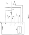
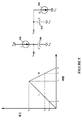
図1を参照すると、本開示の具体的な例示的実施形態に従った、バックスイッチモード電源(SMPS)の概略図が、描写される。概して番号100によって表されるバックSMPSは、パルス幅変調(PWM)生成器102と、ハイサイドスイッチ(例えば、電力MOSFET)104と、ローサイドスイッチ(例えば、電力MOSFET106)と、電力インダクタ108と、出力フィルタコンデンサ110とを備え得る。出力フィルタコンデンサ110を横断する出力電圧(+VSEN、−VSEN)が感知され得る。例えば抵抗器112を横断する電圧降下(+ISEN、−ISEN)もしくはインダクタ108の抵抗自体を使用して、インダクタ108を通る電流を測定するか、または、例えば抵抗器114を横断する電圧降下(ISN、ISP)を使用して、ローサイドスイッチ106を通る電流を測定するかのいずれかによって、出力電流が決定され得る。厳密にいつ電流測定を行うかの決定は、本開示の具体的な例示的実施形態に従った、電流サンプルタイミングおよびトリガ論理200によって決定される。PWM生成器102ならびに電流サンプルタイミングおよびトリガ論理200は、マイクロコントローラの一部であるかまたはマイクロコントローラと協働する機能であり得ることが、想定され、かつ、本開示の範囲内である。PWM生成に関するさらなる詳細および情報が、譲受人のウェブサイトのwww.microchip.com(例えば、アプリケーションノートAN1050、AN564など)において利用可能であり、かつ、あらゆる目的のために、参照することにより、本明細書に援用される。
Referring to FIG. 1, a schematic diagram of a buck switch mode power supply (SMPS) is depicted in accordance with a specific exemplary embodiment of the present disclosure. A back SMPS, generally represented by the
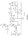
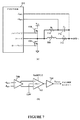
図2を参照すると、本開示の具体的な例示的実施形態に従った、電流サンプルタイミングおよびトリガ論理の概略図が、描写される。概して番号200によって表される電流サンプルタイミングおよびトリガ論理は、一定電流源220と、充電スイッチ(FET)222と、一定電流シンク226と、放電スイッチ(FET)228と、タイミングコンデンサ238と、放電スイッチ(FET)240と、アナログ入力電圧比較器242と、プリスケーラ(n分周器)254と、NANDゲート246およびNANDゲート248と、ANDゲート230と、インバータ224、インバータ232、インバータ234、インバータ244、インバータ250、およびインバータ252とを備え得る。図2に示される回路と同一の機能を実行し得る他の異なる回路構成であって、本開示の利益を有する電子回路設計における当業者によって設計され得る他の異なる回路構成が存在し得ることが、想定され、かつ、本開示の範囲内である。
Referring to FIG. 2, a schematic diagram of current sample timing and trigger logic is depicted in accordance with a specific exemplary embodiment of the present disclosure. The current sample timing and trigger logic, generally represented by the
充電スイッチ222がオンになると、一定電流源220は、Iの一定電流においてタイミングコンデンサ238を充電し始め、タイミングコンデンサ238上の電荷が、経時的に線形に増加することにより、充電電圧を作り出す。放電スイッチ228がオンになると、一定電流シンク226は、タイミングコンデンサ238上の電荷を放電し始める。充電スイッチ222および放電スイッチ228がそれぞれ両方ともオンであるとき、タイミングコンデンサ226の充電/放電は、一定電流源220と一定電流シンク226との間の電流差となる。一定電流シンク226は2Iの一定電流値を有し、かつ、一定電流源220はIの一定電流値を有するため、スイッチ222およびスイッチ228の両方がオンであるとき、タイミングコンデンサ238は、Iの一定電流において放電される。スイッチ222のみがオンであるとき、一定電流源220は、Iの一定電流においてタイミングコンデンサ238を充電する。スイッチ228のみがオンであるとき、一定電流シンク226は、2Iの一定電流においてタイミングコンデンサ238を放電する。
When the charging
電流感知経路からのSAMPLE信号は、PWM信号のスイッチング周波数に等しい速度で発生する。図2に示される論理によってSAMPLE信号が生成されると、SAMPLE信号はまた、基準電圧までタイミングコンデンサ238を事前充電(電圧等化)するようにスイッチ240を制御し得、スイッチ240は、電圧比較器242の非反転入力にも結合される。この基準電圧は、一実施形態によると、例えば、0.7ボルト(V)であり得るが、これに限定されない。しかしながら、他の基準電圧(例えば、0.0ボルト)が使用され得る。
The SAMPLE signal from the current sensing path is generated at a rate equal to the switching frequency of the PWM signal. When the SAMPLE signal is generated by the logic shown in FIG. 2, the SAMPLE signal may also control the
PMW周期は、アナログ/デジタルコンバータ(ADC)(図示せず)がアナログ電流サンプルをそのデジタル表現に変換するよりも早くあり得る。したがって、プリスケーラ254(n除算回路)は、SAMPLE信号と、ADC変換を開始するために使用されるADC変換トリガ信号との間に必要とされ得る。アナログ電流値のサンプルが、依然として、ローサイドの50%点毎に取得され得るが、ADCによる変換のためにともに平均化され得る。NANDゲート230およびNANDゲート234と、インバータ232およびインバータ236とを備えるフリップフロップ回路を使用して、50%PWM周期信号は、スイッチ228をオンにし、これは、SAMPLE信号がアサートされるまでオンのままである。
The PMW period can be faster than an analog to digital converter (ADC) (not shown) converts the analog current sample into its digital representation. Thus, a prescaler 254 (n divider circuit) may be required between the SAMPLE signal and the ADC conversion trigger signal used to initiate the ADC conversion. Samples of the analog current value can still be taken every 50% of the low side, but can be averaged together for conversion by the ADC. Using a flip-flop circuit comprising
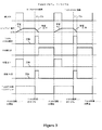
図3を参照すると、本開示の具体的な例示的実施形態に従った、20パーセントのPWMデューティサイクルにおける、図2に示される電流サンプルタイミングおよびトリガ論理の概略的なタイミング図が、描写される。PWMデューティサイクルが50%を下回ると、SAMPLE信号が、以下の説明に従って生成され、SAMPLE信号が、図3に描写される。コンデンサ238は、ハイドライブ(HI_ON)がアサート(オンに)される(ハイサイドスイッチ104がオンである)ときのみ、一定電流源220からのIに等しい一定電流を用いて充電され、充電スイッチ222を導通させ(オンにさせ)、それによって、一定電流源220をタイミングコンデンサ238に結合する。タイミングコンデンサ238は、すでに0.7Vまで充電されており、一定充電電流Iは、タイミングコンデンサ238上の電圧電荷をさらに増加させる。ハイドライブ(HI_ON)がデアサート(オフに)される(ハイサイドスイッチ104がオフになる)まで、充電スイッチ222は、オンのままであり、かつ、一定電流源220は、タイミングコンデンサ238に結合されたままである。
Referring to FIG. 3, a schematic timing diagram of the current sample timing and trigger logic shown in FIG. 2 at a 20 percent PWM duty cycle is depicted, in accordance with a specific exemplary embodiment of the present disclosure. . When the PWM duty cycle is below 50%, a SAMPLE signal is generated according to the following description and the SAMPLE signal is depicted in FIG.
PWMスイッチング周期が50%に到達する前にハイサイドスイッチ104がオフになる場合、充電スイッチ222は、オフになり、コンデンサ238上の電荷は、保持される。電流源220および/または電流シンク226がタイミングコンデンサ238に結合されていない場合、タイミングコンデンサ238上に電荷(電圧)が維持される。PWMスイッチング周期が50%に到達すると、スイッチ228は、オンになり、電流シンク226は、タイミングコンデンサ238に結合され、それによって、2Iの一定電流率においてタイミングコンデンサ238上の電圧電荷を放電する。したがって、コンデンサ238は、コンデンサ238が充電されたときよりも2倍早く放電する。コンデンサ238上の電圧電荷が0.7Vであるとき、負荷電流がサンプリングされる時点に到達する。このサンプリング点は、ローサイドスイッチ106の導通時間の中間点と一致する。
If the
PWM周期50%点で開始すると、タイミングコンデンサ238上の電圧は、一定電流シンク226がタイミングコンデンサ238に結合されている限り、タイミングコンデンサ238上の電圧が0.7Vに到達するまで減少し続け、電圧比較器242の出力は、高になり、インバータ244の出力は、低になり、NANDゲート246の出力は、高になる。これは、ハイドライブ(HI_ON)がデアサート(オフに)されるため、NANDゲート248の出力を低にさせる。NANDゲート248の出力が低になると、インバータ252の出力は高になり、SAMPLE信号が生成され、FETスイッチ240をオンにさせ、それによって、タイミングコンデンサ238上の電圧をもとの0.7Vにリセットする(異なる電圧における場合)。SAMPLE信号は、ローサイドスイッチ106がオンであるときの中間点で高になる。したがって、インダクタ108を通る電流のサンプルは、インダクタ電流の中間点または平均において取得される。
Starting at the 50% PWM period, the voltage on the
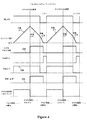
図4を参照すると、本開示の具体的な例示的実施形態に従った、80パーセントのPWMデューティサイクルにおける、図2に示される電流サンプルタイミングおよびトリガ論理の概略的なタイミング図が、描写される。PWMデューティサイクルが50%を上回ると、SAMPLE信号が、以下の説明に従って生成され、SAMPLE信号が、図4に描写される。コンデンサ238は、ハイドライブ(HI_ON)がアサート(オンに)される(ハイサイドスイッチ104がオンである)ときのみ、一定電流源220からのIに等しい一定電流を用いて充電され、充電スイッチ222を導通させ(オンにさせ)、それによって、一定電流源220をタイミングコンデンサ238に結合する。タイミングコンデンサ238は、すでに0.7Vまで充電されており、一定充電電流Iは、タイミングコンデンサ238上の電圧電荷をさらに増加させる。ハイドライブ(HI_ON)がデアサート(オフに)されるまで、充電スイッチ222は、オンのままであり、一定電流源は、タイミングコンデンサ238に結合されたままである。PWM周期50%点において、スイッチ228は、オンにされ、電流シンク226もまた、タイミングコンデンサ238に結合され、それによって、電流源220がタイミングコンデンサ238に結合されたままであるため、Iの一定電流率においてタイミングコンデンサ238上の電圧電荷を放電する。
Referring to FIG. 4, a schematic timing diagram of the current sample timing and trigger logic shown in FIG. 2 at 80 percent PWM duty cycle is depicted, in accordance with a specific exemplary embodiment of the present disclosure. . When the PWM duty cycle exceeds 50%, a SAMPLE signal is generated according to the following description and the SAMPLE signal is depicted in FIG.
ハイサイドスイッチ104がオフになると、スイッチ222は、低になるハイサイドドライブ(HI_ON)によってオフにされる。次いで、タイミングコンデンサ238上の電圧は、タイミングコンデンサ238上の電圧が0.7Vに到達するまで、タイミングコンデンサ238が充電された速度の2倍で減少する。電圧比較器242の出力が高になると、インバータ244の出力は低になり、NANDゲート246の出力は高になる。これは、ハイドライブ(HI_ON)がデアサート(オフに)されるため、NANDゲート248の出力を低にさせる。NANDゲート248の出力が低になると、インバータ252の出力は高になり、SAMPLE信号が生成され、それによって、タイミングコンデンサ238上の電圧をもとの0.7Vにリセットする(異なる電圧における場合)。SAMPLE信号は、ローサイドスイッチ106がオンであるときの中間点で高になる。したがって、インダクタ108を通る電流のサンプルは、インダクタ電流の中間点または平均において取得される。
When the
図5を参照すると、本開示の具体的な例示的実施形態に従った、一定電流源から充電されかつシンクから放電されているコンデンサの概略的な時間−電圧グラフが、描写される。図2に示されるアナログタイミング回路の機能は、図5を参照することによって、より良く理解され得、図5では、一定電流源520から充電されかつ一定電流シンク526によって放電されているコンデンサ538の時間−電圧グラフが描写される。コンデンサ538が一定電流源520を通して充電されると、コンデンサ518を横断する電圧Vcapは、方程式I=C×dV/dtに従って、時間とともに線形に増加し、式中、Cは、コンデンサ538の容量値であり、Iは、一定電流源520からの電流であり、Vは、時間tにおけるコンデンサ538上の電圧である。電流I、時間t、および電圧Vのうちの任意の2つの値が既知であるとき、他の未知の値は、2つの既知の値から計算され得る。例えば、コンデンサ538の容量と、一定電流源520からの充電電流とが既知である場合、電圧V1における時間t1および電圧V2における時間t2は、上記の方程式(1)を使用して決定され得る。同様に、コンデンサ538上の電圧は、一定電流シンク526をコンデンサ538に結合することによって放電され得る。一定電流シンク526が2Iの一定電流または一定電流源520の2倍の一定電流値を有するとき、タイミングコンデンサ538は、一定電流Iにおいてタイミングコンデンサ538が充電されたときの2倍早く(2I)放電される。一定電流シンク526が一定電流源520の電流値の実質的に2倍である場合、タイミングコンデンサ538は、一定電流シンク526のみがタイミングコンデンサ538に結合されているときは、常時、タイミングコンデンサ538が充電された速度の2倍で放電される。タイミングコンデンサの一定電流充電および放電のための用途のより一般的な使用説明が、www.microchip.comにおいて利用可能なMicrochipアプリケーションノートAN1250およびAN1375、ならびに、「Measuring a long time period」と題された共有の米国特許第7,460,441号B2および「Current−time digital−to−analogconverter」と題された米国特許第7,764,213号B2(両方とも、James E. Bartlingによる)においてより完全に説明され、全てが、あらゆる目的のために、参照することにより、本明細書に援用される。
Referring to FIG. 5, a schematic time-voltage graph of a capacitor charged from a constant current source and discharged from a sink, according to a specific exemplary embodiment of the present disclosure, is depicted. The function of the analog timing circuit shown in FIG. 2 can be better understood by referring to FIG. 5, in which the
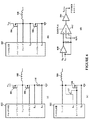
図6を参照すると、本開示の具体的な例示的実施形態に従った、インダクタ電流測定回路の概略図が、描写される。電流測定回路が図6(a)に示され、ローサイド電流が電流測定回路を通過するときに抵抗器114が電圧を生じさせる。図6(b)では、スイッチ(FET)106の内部抵抗が、抵抗器114の代わりに使用される。図6(c)では、感知またはパイロットFET107が、電流感知要素として使用され得る。小型パイロットFET107を通る電流が、抵抗器114を横断して生じる電圧の代わりに使用され得る。パイロットFET107は、主要電力FET106に内蔵されるかまたは主要電力FET106とともにパッケージ化され得、典型的には、主要電力FET106よりもはるかに大きいRDSonを有する。例えば、この設計は、10,000:1のRDSon比で、パイロットFET107を用いて電力FET106への電流を感知することが可能であり得る。これらの電流測定回路の全ては、ローサイドスイッチ106の導通中にインダクタ108を通る電流のアナログパラメータ指示を提供する。
Referring to FIG. 6, a schematic diagram of an inductor current measurement circuit is depicted in accordance with a specific exemplary embodiment of the present disclosure. A current measurement circuit is shown in FIG. 6 (a), where the
図6(d)を参照すると、入力端子ISNおよび入力端子ISP上のインダクタ電流信号は、差動入力増幅器660に印加され、次いで、SAMPLE信号アサーション毎に電圧サンプルを取得し得るサンプルホールド回路662に印加され得、電圧オフセット(例えば、0.5V)を導入させ得る。電圧オフセットは、誤差増幅器が軽負荷条件下で狭いデューティサイクルを制御することが可能なように使用される。典型的には、レールツーレール出力増幅器でさえ、電圧レールに至るまで駆動することはできない。この電圧オフセットは、誤差増幅器が、全てのデューティサイクル条件に対する制御を維持することを可能にする。増幅器664はさらに、ADC(図示せず)による変換のためにISENSE信号を調整および/または増幅し得る。ADCは、SAMPLE信号が発生するn回目毎にISENSE信号をそのデジタル表現に変換し得る。アナログ電流値のサンプルが、ローサイドの50%点毎に取得され、かつ、ADCによってデジタル値に変換される前にともに平均化され得る。
Referring to FIG. 6 (d), the inductor current signal on the input terminal I SN and the input terminal I SP is applied to the
図7を参照すると、本開示の他の具体的な例示的実施形態に従った、インダクタ電流測定回路の概略図が、描写される。インダクタ電流感知要素は、負荷への出力と直列の抵抗器112(図1)、または、インダクタ708の直列抵抗712のいずれかであり得る。インダクタ708の直列抵抗712が使用される場合、RCフィルタが、図7(a)に示されるように、インダクタ708付近に置かれ得る。抵抗器770(RS)およびコンデンサ772(CS)の値は、以下の公式を使用することによって決定され得る。
L/RL=RS×CSであり、式中、
Lは、出力インダクタ708のインダクタンス値であり、
RLは、出力インダクタ708の直列抵抗712であり、
RSは、電流感知フィルタ抵抗器770であり、
CSは、電流感知フィルタコンデンサ772である。
Referring to FIG. 7, a schematic diagram of an inductor current measurement circuit is depicted, according to another specific exemplary embodiment of the present disclosure. The inductor current sensing element can be either a resistor 112 (FIG. 1) in series with the output to the load or a
L / R L = R S × C S where
L is the inductance value of the
R L is the
R S is a current
CS is a current
電流感知フィルタの時定数がインダクタの時定数に等しく設定されるとき、コンデンサ772(CS)を横断して出現する電圧は、インダクタ708内を流れる電流をインダクタ708の直列抵抗712で乗算したものに近似する。
When the time constant of the current sense filter is set equal to the time constant of the inductor, the voltage appearing across capacitor 772 (C S ) is the current flowing in
図7(b)を参照すると、入力端子ISNおよび入力端子ISP上のインダクタ電流信号は、差動入力増幅器760に印加され、次いで、SAMPLE信号アサーション毎に電圧サンプルを取得し得るサンプルホールド回路762に印加され得、電圧オフセット(例えば、0.5V)を導入させ得る。電圧オフセットは、誤差増幅器が軽負荷条件下で狭いデューティサイクルを制御することが可能なように使用される。典型的には、レールツーレール出力増幅器であさえ、電圧レールに至るまで駆動することはできない。この電圧オフセットは、誤差増幅器が、全てのデューティサイクル条件に対する制御を維持することを可能にする。サンプリングされた電流および測定された出力電流の両方が、制御のために使用され得る。増幅器764は、ADC(図示せず)による変換のためにISENSE信号をさらに調整および/または増幅し得る。ADCは、SAMPLE信号が発生するn回目毎にISENSE信号をそのデジタル表現に変換し得る。アナログ電流値のサンプルが、ローサイドの50%点毎に取得され、かつ、ADCによってデジタル値に変換される前にともに平均化され得る。
Referring to FIG. 7 (b), the inductor current signal on the input terminal I SN and the input terminal I SP is applied to the
本明細書に説明される回路全体は、好ましくは、ACD、PWM生成器、および充電時間測定ユニット(CTMU)を有するマイクロコントローラ内に実装され得る。構成可能な論理が、上記に議論される実施形態のうちの1つに従った構成を可能にするようにマイクロコントローラ内に存在し得るしかしながら、CTMUの具体的な実装により、要求される回路がすでに提供されていてもよい。ファームウェアが、特にSMPS用途のためにソフトウェアオーバーヘッドを殆ど伴わずに電流を自動的に測定するように、それぞれの回路を制御し得る。 The entire circuit described herein can preferably be implemented in a microcontroller having an ACD, a PWM generator, and a charge time measurement unit (CTMU). Configurable logic may be present in the microcontroller to allow configuration according to one of the embodiments discussed above, however, the specific implementation of the CTMU will result in the required circuit being It may already be provided. Each circuit may be controlled so that the firmware automatically measures current with little software overhead, especially for SMPS applications.
Claims (20)
前記ハイサイドスイッチがオンであるとき、第1の一定電流を用いてタイミングコンデンサを充電するステップと、
パルス幅変調(PWM)周期が50%に到達しかつ前記ハイサイドスイッチがオンであるとき、前記第1の一定電流を用いて前記タイミングコンデンサを放電するステップと、
前記PWM周期が50%に到達しかつ前記ハイサイドスイッチがオフであるとき、第2の一定電流を用いて前記タイミングコンデンサを放電するステップであって、前記第2の一定電流は、前記第1の一定電流の2倍である、ステップと、
前記タイミングコンデンサ上の電圧が所定の基準電圧に到達すると、電力インダクタ電流をサンプリングするステップと、
を含む、方法。 A switched mode power supply having a high side switch and a low side switch coupled in series between a supply voltage and a supply common, and a power inductor coupled between a junction of the high side switch and the low side switch and a load A method for performing current measurements in (SMPS), the method comprising:
Charging the timing capacitor with a first constant current when the high side switch is on;
Discharging the timing capacitor using the first constant current when a pulse width modulation (PWM) period reaches 50% and the high-side switch is on;
Discharging the timing capacitor with a second constant current when the PWM period reaches 50% and the high-side switch is off, wherein the second constant current is the first constant current; A step that is twice the constant current of
Sampling the power inductor current when the voltage on the timing capacitor reaches a predetermined reference voltage;
Including a method.
アナログ/デジタルコンバータ(ADC)を用いて前記複数の電力インダクタ電流サンプルの平均を前記複数の電力インダクタ電流サンプルの平均のデジタル表現に変換するステップと
をさらに含む、請求項1に記載の方法。 Averaging a plurality of said power inductor current samples;
The method of claim 1, further comprising: converting an average of the plurality of power inductor current samples into a digital representation of the average of the plurality of power inductor current samples using an analog / digital converter (ADC).
前記ローサイドスイッチと前記供給コモンとの間に電流測定抵抗器を提供するステップと、
前記タイミングコンデンサ上の電圧が前記所定の基準電圧に到達すると、前記電流測定抵抗器を横断して生じた電圧をサンプリングするステップと
を含む、請求項1に記載の方法。 Sampling the power inductor current comprises:
Providing a current measuring resistor between the low side switch and the supply common;
The method of claim 1, comprising: sampling a voltage generated across the current measuring resistor when a voltage on the timing capacitor reaches the predetermined reference voltage.
前記ローサイドMOSFETに関連付けられるパイロット電界効果トランジスタ(FET)を提供するステップであって、前記パイロットFETは、前記電力インダクタを通って流れる前記電力インダクタ電流のごく一部を有する、ステップと、
前記タイミングコンデンサ上の電圧が前記所定の基準電圧に到達すると、前記パイロットFETおよび前記ローサイドMOSFETを横断して生じた電圧をサンプリングするステップと、
を含む、請求項8に記載の方法。 Sampling the power inductor current comprises:
Providing a pilot field effect transistor (FET) associated with the low-side MOSFET, wherein the pilot FET has a fraction of the power inductor current flowing through the power inductor;
Sampling the voltage generated across the pilot FET and the low-side MOSFET when the voltage on the timing capacitor reaches the predetermined reference voltage;
The method of claim 8 comprising:
前記電力インダクタと直列に電流測定抵抗器を提供するステップと、
前記タイミングコンデンサ上の電圧が前記所定の基準電圧に到達すると、前記電流測定抵抗器を横断して生じた電圧をサンプリングするステップと、
を含む、請求項1に記載の方法。 Sampling the power inductor current comprises:
Providing a current measuring resistor in series with the power inductor;
Sampling the voltage generated across the current measuring resistor when the voltage on the timing capacitor reaches the predetermined reference voltage;
The method of claim 1 comprising:
第1のノードおよび第2のノードを有する一定電流源であって、前記一定電流源の第1のノードは、電圧源に結合される、一定電流源と、
第1のノードおよび第2のノードを有する一定電流シンクであって、前記一定電流シンクは、前記一定電流源の電流値の2倍である、一定電流シンクと、
前記一定電流源の第2のノードと前記一定電流シンクの第1のノードとの間に結合される電流源スイッチと、
前記一定電流シンクの第2のノードと電圧源コモンとの間に結合される電流シンクスイッチと、
前記一定電流シンクの第1のノードと前記電圧源コモンとの間に結合されるタイミングコンデンサと、
所定の基準電圧に結合される第1の入力と、前記タイミングコンデンサに結合される第2の入力と、出力とを有する電圧比較器であって、前記電圧比較器の前記出力は、前記タイミングコンデンサ上の電圧が前記所定の基準電圧を上回るとき、第1の論理レベルにあり、前記タイミングコンデンサ上の電圧が前記所定の基準電圧に等しいかまたは前記所定の基準電圧を下回るとき、第2の論理レベルにある、電圧比較器と、
を備え、
前記SMPSからのハイサイドスイッチ信号が第1の論理レベルになると、前記電流源スイッチは、オンになり、かつ、前記一定電流源を前記タイミングコンデンサに結合し、それによって、前記タイミングコンデンサ上の電圧は増加し、
前記SMPSからのハイサイドスイッチ信号が第2の論理レベルになると、前記電流源スイッチは、オフになり、かつ、前記一定電流源を前記タイミングコンデンサから分離し、それによって、前記タイミングコンデンサ上の電圧は同一のままであり、
前記SMPSからの50%パルス幅変調(PWM)周期信号が受信されると、前記電流シンクスイッチは、オンになり、かつ、前記一定電流シンクを前記タイミングコンデンサに結合し、それによって、前記タイミングコンデンサ上の電圧は、前記ハイサイドスイッチ信号が前記第2の論理レベルにあるとき、前記タイミングコンデンサ上の電圧が増加したときよりも2倍早く減少し、前記ハイサイドスイッチ信号が前記第1の論理レベルにあるとき、前記タイミングコンデンサ上の電圧は、前記タイミングコンデンサ上の電圧が増加したときと同一の速度で減少する、装置。 An apparatus for determining a power inductor current sample point in a buck switch mode power supply (SMPS), the apparatus comprising:
A constant current source having a first node and a second node, wherein the first node of the constant current source is coupled to a voltage source;
A constant current sink having a first node and a second node, wherein the constant current sink is twice the current value of the constant current source;
A current source switch coupled between the second node of the constant current source and the first node of the constant current sink;
A current sink switch coupled between a second node of the constant current sink and a voltage source common;
A timing capacitor coupled between a first node of the constant current sink and the voltage source common;
A voltage comparator having a first input coupled to a predetermined reference voltage, a second input coupled to the timing capacitor, and an output, wherein the output of the voltage comparator is the timing capacitor When the upper voltage is above the predetermined reference voltage, it is at a first logic level, and when the voltage on the timing capacitor is equal to or less than the predetermined reference voltage, a second logic level A voltage comparator at the level,
With
When the high side switch signal from the SMPS is at a first logic level, the current source switch is turned on and couples the constant current source to the timing capacitor, thereby causing a voltage on the timing capacitor. Will increase,
When the high side switch signal from the SMPS goes to a second logic level, the current source switch is turned off and isolates the constant current source from the timing capacitor, thereby causing a voltage on the timing capacitor. Remain the same,
When a 50% pulse width modulation (PWM) periodic signal from the SMPS is received, the current sink switch turns on and couples the constant current sink to the timing capacitor, thereby the timing capacitor The upper voltage decreases two times faster when the high side switch signal is at the second logic level than when the voltage on the timing capacitor is increased, and the high side switch signal is reduced to the first logic level. When at level, the voltage on the timing capacitor decreases at the same rate as the voltage on the timing capacitor increases.
Applications Claiming Priority (5)
| Application Number | Priority Date | Filing Date | Title |
|---|---|---|---|
| US201462065152P | 2014-10-17 | 2014-10-17 | |
| US62/065,152 | 2014-10-17 | ||
| US14/883,381 US9778289B2 (en) | 2014-10-17 | 2015-10-14 | Measuring output current in a buck SMPS |
| US14/883,381 | 2015-10-14 | ||
| PCT/US2015/055859 WO2016061426A1 (en) | 2014-10-17 | 2015-10-16 | Measuring output current in a buck smps |
Publications (2)
| Publication Number | Publication Date |
|---|---|
| JP2017531418A true JP2017531418A (en) | 2017-10-19 |
| JP2017531418A5 JP2017531418A5 (en) | 2018-11-08 |
Family
ID=54364753
Family Applications (1)
| Application Number | Title | Priority Date | Filing Date |
|---|---|---|---|
| JP2017519887A Ceased JP2017531418A (en) | 2014-10-17 | 2015-10-16 | Measurement of output current in buck SMPS |
Country Status (7)
| Country | Link |
|---|---|
| US (2) | US9778289B2 (en) |
| EP (1) | EP3207627B1 (en) |
| JP (1) | JP2017531418A (en) |
| KR (1) | KR20170071473A (en) |
| CN (1) | CN106664018B (en) |
| TW (2) | TWI688775B (en) |
| WO (1) | WO2016061426A1 (en) |
Families Citing this family (18)
| Publication number | Priority date | Publication date | Assignee | Title |
|---|---|---|---|---|
| US9778289B2 (en) * | 2014-10-17 | 2017-10-03 | Microchip Technology Incorporated | Measuring output current in a buck SMPS |
| CN106130319B (en) * | 2016-08-22 | 2019-04-16 | 昂宝电子(上海)有限公司 | A kind of system and method for driving power transistor |
| US10199929B2 (en) * | 2016-10-03 | 2019-02-05 | Texas Instruments Incorporated | Transient event detector circuit and method |
| US9853548B1 (en) * | 2017-02-06 | 2017-12-26 | Alpha And Omega Semiconductor Incorporated | Accurate high-side current emulation with auto-conversion for smart power stage applications |
| US10063146B1 (en) * | 2017-03-31 | 2018-08-28 | Alpha And Omega Semiconductor (Cayman) Ltd. | Full-time inductor current monitoring method by sensing low side switch |
| CN107132404B (en) * | 2017-05-15 | 2019-11-05 | 矽力杰半导体技术(杭州)有限公司 | Detection method, detection circuit, controller and Switching Power Supply |
| KR102281654B1 (en) | 2017-06-08 | 2021-07-29 | 현대자동차주식회사 | Hybrid vehicle and method for controlling thereof |
| US10361684B2 (en) * | 2017-07-19 | 2019-07-23 | Invecas, Inc. | Duty cycle detection |
| CN107493099B (en) * | 2017-08-22 | 2021-11-26 | 钰泰半导体股份有限公司 | Method for setting chip working mode |
| US10056819B1 (en) * | 2017-10-24 | 2018-08-21 | Texas Instruments Incorporated | Predicting the timing of current phases of a DC-DC converter |
| TWI650922B (en) * | 2018-02-07 | 2019-02-11 | 新唐科技股份有限公司 | Half bridge circuit driving chip with protection circuit and protection method thereof |
| JP2019149614A (en) * | 2018-02-26 | 2019-09-05 | ルネサスエレクトロニクス株式会社 | Current detection circuit, semiconductor device, and semiconductor system |
| CN109450016B (en) * | 2018-10-29 | 2020-11-03 | Oppo广东移动通信有限公司 | Discharging method, mobile power supply and computer storage medium |
| US10830799B1 (en) | 2019-07-12 | 2020-11-10 | Alpha And Omega Semiconductor (Cayman) Ltd. | Temperature and VGS compensation for current sensing using Rdson in MOSFETS |
| CN110768510B (en) | 2019-09-30 | 2022-09-20 | 上海矽力杰微电子技术有限公司 | Control circuit and method and power converter |
| TWI728588B (en) | 2019-12-11 | 2021-05-21 | 茂達電子股份有限公司 | Current detecting circuit and method for constant on-time power converter |
| US11469669B2 (en) * | 2020-01-31 | 2022-10-11 | Texas Instruments Incorporated | Methods and circuitry to detect PFM mode entry in wide duty range DC converter |
| KR102624192B1 (en) * | 2021-11-30 | 2024-01-11 | 한국과학기술원 | Precharge method and precharge circuit using the same |
Family Cites Families (19)
| Publication number | Priority date | Publication date | Assignee | Title |
|---|---|---|---|---|
| US5835361A (en) * | 1997-04-16 | 1998-11-10 | Thomson Consumer Electronics, Inc. | Switch-mode power supply with over-current protection |
| US7026797B2 (en) * | 2003-03-21 | 2006-04-11 | Tropian, Inc. | Extremely high-speed switchmode DC-DC converters |
| CN1856929A (en) * | 2003-09-25 | 2006-11-01 | 皇家飞利浦电子股份有限公司 | A switch mode power converter |
| US7362191B2 (en) * | 2004-04-29 | 2008-04-22 | Linear Technology Corporation | Methods and circuits for frequency modulation that reduce the spectral noise of switching regulators |
| US7274183B1 (en) | 2005-11-02 | 2007-09-25 | National Semiconductor Corporation | Versatile system for high-power switching controller in low-power semiconductor technology |
| GB0615029D0 (en) * | 2005-12-22 | 2006-09-06 | Cambridge Semiconductor Ltd | Switch mode power supply controllers |
| US7460441B2 (en) | 2007-01-12 | 2008-12-02 | Microchip Technology Incorporated | Measuring a long time period |
| US7764213B2 (en) | 2008-07-01 | 2010-07-27 | Microchip Technology Incorporated | Current-time digital-to-analog converter |
| US8525498B2 (en) | 2008-07-31 | 2013-09-03 | Monolithic Power Systems, Inc. | Average input current limit method and apparatus thereof |
| JP2010103707A (en) * | 2008-10-22 | 2010-05-06 | Canon Inc | Charge pumping circuit and clock generator |
| CN103427647B (en) * | 2012-05-22 | 2016-02-17 | 通嘉科技股份有限公司 | Power supply unit and power-supply controller of electric |
| AT512780B1 (en) * | 2012-06-13 | 2013-11-15 | Fronius Int Gmbh | Switching power supply and inverter and strand monitoring with such a switching power supply |
| US9285399B2 (en) | 2012-06-29 | 2016-03-15 | Infineon Technologies Austria Ag | Switching regulator cycle-by-cycle current estimation |
| CN102891611B (en) * | 2012-06-30 | 2014-10-08 | 华为技术有限公司 | Five-level power converter, and control method and control device for five-level power converter |
| CN102820781B (en) * | 2012-08-30 | 2014-08-06 | 东南大学 | Single-inductance double-output switch power supply based on ripple control |
| US9564810B2 (en) * | 2013-03-28 | 2017-02-07 | Infineon Technologies Austria Ag | Switched mode power supply |
| TWM472362U (en) * | 2013-08-07 | 2014-02-11 | Richtek Technology Corp | Buck switching regulator |
| CN103532555A (en) * | 2013-10-23 | 2014-01-22 | 电子科技大学 | Voltage comparator based on voltage-controlled oscillators |
| US9778289B2 (en) * | 2014-10-17 | 2017-10-03 | Microchip Technology Incorporated | Measuring output current in a buck SMPS |
-
2015
- 2015-10-14 US US14/883,381 patent/US9778289B2/en active Active
- 2015-10-16 WO PCT/US2015/055859 patent/WO2016061426A1/en active Application Filing
- 2015-10-16 EP EP15787391.0A patent/EP3207627B1/en not_active Not-in-force
- 2015-10-16 KR KR1020177006189A patent/KR20170071473A/en unknown
- 2015-10-16 CN CN201580045951.3A patent/CN106664018B/en not_active Expired - Fee Related
- 2015-10-16 TW TW108119510A patent/TWI688775B/en not_active IP Right Cessation
- 2015-10-16 JP JP2017519887A patent/JP2017531418A/en not_active Ceased
- 2015-10-16 TW TW104134090A patent/TW201625967A/en unknown
-
2017
- 2017-10-02 US US15/723,115 patent/US10114046B2/en active Active
Also Published As
| Publication number | Publication date |
|---|---|
| US9778289B2 (en) | 2017-10-03 |
| WO2016061426A1 (en) | 2016-04-21 |
| EP3207627B1 (en) | 2019-10-16 |
| TW201937178A (en) | 2019-09-16 |
| TW201625967A (en) | 2016-07-16 |
| US20180024171A1 (en) | 2018-01-25 |
| US10114046B2 (en) | 2018-10-30 |
| CN106664018B (en) | 2019-09-03 |
| EP3207627A1 (en) | 2017-08-23 |
| TWI688775B (en) | 2020-03-21 |
| US20160109488A1 (en) | 2016-04-21 |
| CN106664018A (en) | 2017-05-10 |
| KR20170071473A (en) | 2017-06-23 |
Similar Documents
| Publication | Publication Date | Title |
|---|---|---|
| US10114046B2 (en) | Measuring output current in a buck SMPS | |
| JP2017531418A5 (en) | ||
| TWI519044B (en) | A system and method for adjusting the output current of a power conversion system | |
| US10090751B1 (en) | Gate driver for switching converter having body diode power loss minimization | |
| US20130182476A1 (en) | Adaptive sampling circuit for detecting the demagnetized voltage of the transformer | |
| US9559592B2 (en) | Synchronous rectifier timer for discontinuous mode DC/DC converter | |
| JP5418899B2 (en) | Control circuit for use in power converter and method for preventing transformer saturation in power converter | |
| US9450487B2 (en) | DC to DC converter | |
| CN110022051B (en) | Device and method for driving a power stage | |
| US8587275B2 (en) | Instantaneous average current measurement method | |
| US11323110B2 (en) | Duty timing detector detecting duty timing of toggle signal, device including duty timing detector, and operating method of device receiving toggle signal | |
| CN105978317A (en) | Switching power supply device control circuit and switching power supply device | |
| JP7177340B2 (en) | Semiconductor device for switching power supply and AC-DC converter | |
| US9857395B2 (en) | Method and apparatus for measuring average inductor current delivered to a load | |
| US7982452B2 (en) | Detection of a load state of a half-bridge | |
| US10340796B2 (en) | Constant on time boost converter control | |
| US10468981B2 (en) | Switching power supply device | |
| US9077294B2 (en) | Measurement of the output current of an amplifier circuit | |
| JP6853684B2 (en) | DC / DC converter and its control circuit, control method and in-vehicle electrical equipment | |
| JP2009254061A (en) | Semiconductor integrated circuit and its test method | |
| WO2020129414A1 (en) | Integrated circuit and power supply circuit | |
| US9541989B2 (en) | Power transfer estimation | |
| JP7107314B2 (en) | DC-DC converter, method for measuring voltage drop due to switch element, method for detecting failure of switch element, three-phase inverter | |
| TWI697186B (en) | Converting apparatus and method thereof | |
| TWM445301U (en) | Voltage converting apparatus and sub-harmonic detector thereof |
Legal Events
| Date | Code | Title | Description |
|---|---|---|---|
| A521 | Written amendment |
Free format text: JAPANESE INTERMEDIATE CODE: A523 Effective date: 20180928 |
|
| A621 | Written request for application examination |
Free format text: JAPANESE INTERMEDIATE CODE: A621 Effective date: 20180928 |
|
| A01 | Written decision to grant a patent or to grant a registration (utility model) |
Free format text: JAPANESE INTERMEDIATE CODE: A01 Effective date: 20190719 |
|
| A977 | Report on retrieval |
Free format text: JAPANESE INTERMEDIATE CODE: A971007 Effective date: 20190717 |
|
| A045 | Written measure of dismissal of application [lapsed due to lack of payment] |
Free format text: JAPANESE INTERMEDIATE CODE: A045 Effective date: 20191121 |