JP2017524328A - Switch mode power supply - Google Patents
Switch mode power supply Download PDFInfo
- Publication number
- JP2017524328A JP2017524328A JP2017506783A JP2017506783A JP2017524328A JP 2017524328 A JP2017524328 A JP 2017524328A JP 2017506783 A JP2017506783 A JP 2017506783A JP 2017506783 A JP2017506783 A JP 2017506783A JP 2017524328 A JP2017524328 A JP 2017524328A
- Authority
- JP
- Japan
- Prior art keywords
- auxiliary
- power supply
- mode power
- switch mode
- inductor
- Prior art date
- Legal status (The legal status is an assumption and is not a legal conclusion. Google has not performed a legal analysis and makes no representation as to the accuracy of the status listed.)
- Pending
Links
- 239000003990 capacitor Substances 0.000 claims description 27
- 238000013016 damping Methods 0.000 claims description 4
- 238000010586 diagram Methods 0.000 description 6
- 230000000903 blocking effect Effects 0.000 description 2
- 230000001419 dependent effect Effects 0.000 description 2
- 238000007599 discharging Methods 0.000 description 2
- 238000001514 detection method Methods 0.000 description 1
- 230000005611 electricity Effects 0.000 description 1
- 230000005669 field effect Effects 0.000 description 1
- 238000005259 measurement Methods 0.000 description 1
- 238000000034 method Methods 0.000 description 1
- 238000012986 modification Methods 0.000 description 1
- 230000004048 modification Effects 0.000 description 1
- 238000012544 monitoring process Methods 0.000 description 1
- 230000005693 optoelectronics Effects 0.000 description 1
- 230000010355 oscillation Effects 0.000 description 1
- 239000004065 semiconductor Substances 0.000 description 1
- 238000004804 winding Methods 0.000 description 1
Images


Classifications
-
- H—ELECTRICITY
- H02—GENERATION; CONVERSION OR DISTRIBUTION OF ELECTRIC POWER
- H02M—APPARATUS FOR CONVERSION BETWEEN AC AND AC, BETWEEN AC AND DC, OR BETWEEN DC AND DC, AND FOR USE WITH MAINS OR SIMILAR POWER SUPPLY SYSTEMS; CONVERSION OF DC OR AC INPUT POWER INTO SURGE OUTPUT POWER; CONTROL OR REGULATION THEREOF
- H02M3/00—Conversion of dc power input into dc power output
- H02M3/22—Conversion of dc power input into dc power output with intermediate conversion into ac
- H02M3/24—Conversion of dc power input into dc power output with intermediate conversion into ac by static converters
- H02M3/28—Conversion of dc power input into dc power output with intermediate conversion into ac by static converters using discharge tubes with control electrode or semiconductor devices with control electrode to produce the intermediate ac
- H02M3/325—Conversion of dc power input into dc power output with intermediate conversion into ac by static converters using discharge tubes with control electrode or semiconductor devices with control electrode to produce the intermediate ac using devices of a triode or a transistor type requiring continuous application of a control signal
- H02M3/335—Conversion of dc power input into dc power output with intermediate conversion into ac by static converters using discharge tubes with control electrode or semiconductor devices with control electrode to produce the intermediate ac using devices of a triode or a transistor type requiring continuous application of a control signal using semiconductor devices only
- H02M3/33507—Conversion of dc power input into dc power output with intermediate conversion into ac by static converters using discharge tubes with control electrode or semiconductor devices with control electrode to produce the intermediate ac using devices of a triode or a transistor type requiring continuous application of a control signal using semiconductor devices only with automatic control of the output voltage or current, e.g. flyback converters
-
- H—ELECTRICITY
- H02—GENERATION; CONVERSION OR DISTRIBUTION OF ELECTRIC POWER
- H02M—APPARATUS FOR CONVERSION BETWEEN AC AND AC, BETWEEN AC AND DC, OR BETWEEN DC AND DC, AND FOR USE WITH MAINS OR SIMILAR POWER SUPPLY SYSTEMS; CONVERSION OF DC OR AC INPUT POWER INTO SURGE OUTPUT POWER; CONTROL OR REGULATION THEREOF
- H02M3/00—Conversion of dc power input into dc power output
- H02M3/02—Conversion of dc power input into dc power output without intermediate conversion into ac
- H02M3/04—Conversion of dc power input into dc power output without intermediate conversion into ac by static converters
- H02M3/10—Conversion of dc power input into dc power output without intermediate conversion into ac by static converters using discharge tubes with control electrode or semiconductor devices with control electrode
-
- H—ELECTRICITY
- H02—GENERATION; CONVERSION OR DISTRIBUTION OF ELECTRIC POWER
- H02M—APPARATUS FOR CONVERSION BETWEEN AC AND AC, BETWEEN AC AND DC, OR BETWEEN DC AND DC, AND FOR USE WITH MAINS OR SIMILAR POWER SUPPLY SYSTEMS; CONVERSION OF DC OR AC INPUT POWER INTO SURGE OUTPUT POWER; CONTROL OR REGULATION THEREOF
- H02M3/00—Conversion of dc power input into dc power output
- H02M3/22—Conversion of dc power input into dc power output with intermediate conversion into ac
- H02M3/24—Conversion of dc power input into dc power output with intermediate conversion into ac by static converters
- H02M3/28—Conversion of dc power input into dc power output with intermediate conversion into ac by static converters using discharge tubes with control electrode or semiconductor devices with control electrode to produce the intermediate ac
- H02M3/325—Conversion of dc power input into dc power output with intermediate conversion into ac by static converters using discharge tubes with control electrode or semiconductor devices with control electrode to produce the intermediate ac using devices of a triode or a transistor type requiring continuous application of a control signal
- H02M3/335—Conversion of dc power input into dc power output with intermediate conversion into ac by static converters using discharge tubes with control electrode or semiconductor devices with control electrode to produce the intermediate ac using devices of a triode or a transistor type requiring continuous application of a control signal using semiconductor devices only
- H02M3/33561—Conversion of dc power input into dc power output with intermediate conversion into ac by static converters using discharge tubes with control electrode or semiconductor devices with control electrode to produce the intermediate ac using devices of a triode or a transistor type requiring continuous application of a control signal using semiconductor devices only having more than one ouput with independent control
-
- H—ELECTRICITY
- H02—GENERATION; CONVERSION OR DISTRIBUTION OF ELECTRIC POWER
- H02M—APPARATUS FOR CONVERSION BETWEEN AC AND AC, BETWEEN AC AND DC, OR BETWEEN DC AND DC, AND FOR USE WITH MAINS OR SIMILAR POWER SUPPLY SYSTEMS; CONVERSION OF DC OR AC INPUT POWER INTO SURGE OUTPUT POWER; CONTROL OR REGULATION THEREOF
- H02M3/00—Conversion of dc power input into dc power output
- H02M3/02—Conversion of dc power input into dc power output without intermediate conversion into ac
- H02M3/04—Conversion of dc power input into dc power output without intermediate conversion into ac by static converters
- H02M3/10—Conversion of dc power input into dc power output without intermediate conversion into ac by static converters using discharge tubes with control electrode or semiconductor devices with control electrode
- H02M3/145—Conversion of dc power input into dc power output without intermediate conversion into ac by static converters using discharge tubes with control electrode or semiconductor devices with control electrode using devices of a triode or transistor type requiring continuous application of a control signal
- H02M3/155—Conversion of dc power input into dc power output without intermediate conversion into ac by static converters using discharge tubes with control electrode or semiconductor devices with control electrode using devices of a triode or transistor type requiring continuous application of a control signal using semiconductor devices only
-
- H—ELECTRICITY
- H02—GENERATION; CONVERSION OR DISTRIBUTION OF ELECTRIC POWER
- H02M—APPARATUS FOR CONVERSION BETWEEN AC AND AC, BETWEEN AC AND DC, OR BETWEEN DC AND DC, AND FOR USE WITH MAINS OR SIMILAR POWER SUPPLY SYSTEMS; CONVERSION OF DC OR AC INPUT POWER INTO SURGE OUTPUT POWER; CONTROL OR REGULATION THEREOF
- H02M1/00—Details of apparatus for conversion
- H02M1/08—Circuits specially adapted for the generation of control voltages for semiconductor devices incorporated in static converters
-
- H—ELECTRICITY
- H02—GENERATION; CONVERSION OR DISTRIBUTION OF ELECTRIC POWER
- H02M—APPARATUS FOR CONVERSION BETWEEN AC AND AC, BETWEEN AC AND DC, OR BETWEEN DC AND DC, AND FOR USE WITH MAINS OR SIMILAR POWER SUPPLY SYSTEMS; CONVERSION OF DC OR AC INPUT POWER INTO SURGE OUTPUT POWER; CONTROL OR REGULATION THEREOF
- H02M1/00—Details of apparatus for conversion
- H02M1/14—Arrangements for reducing ripples from dc input or output
-
- H—ELECTRICITY
- H02—GENERATION; CONVERSION OR DISTRIBUTION OF ELECTRIC POWER
- H02M—APPARATUS FOR CONVERSION BETWEEN AC AND AC, BETWEEN AC AND DC, OR BETWEEN DC AND DC, AND FOR USE WITH MAINS OR SIMILAR POWER SUPPLY SYSTEMS; CONVERSION OF DC OR AC INPUT POWER INTO SURGE OUTPUT POWER; CONTROL OR REGULATION THEREOF
- H02M1/00—Details of apparatus for conversion
- H02M1/44—Circuits or arrangements for compensating for electromagnetic interference in converters or inverters
-
- H—ELECTRICITY
- H02—GENERATION; CONVERSION OR DISTRIBUTION OF ELECTRIC POWER
- H02M—APPARATUS FOR CONVERSION BETWEEN AC AND AC, BETWEEN AC AND DC, OR BETWEEN DC AND DC, AND FOR USE WITH MAINS OR SIMILAR POWER SUPPLY SYSTEMS; CONVERSION OF DC OR AC INPUT POWER INTO SURGE OUTPUT POWER; CONTROL OR REGULATION THEREOF
- H02M1/00—Details of apparatus for conversion
- H02M1/0003—Details of control, feedback or regulation circuits
- H02M1/0006—Arrangements for supplying an adequate voltage to the control circuit of converters
-
- H—ELECTRICITY
- H02—GENERATION; CONVERSION OR DISTRIBUTION OF ELECTRIC POWER
- H02M—APPARATUS FOR CONVERSION BETWEEN AC AND AC, BETWEEN AC AND DC, OR BETWEEN DC AND DC, AND FOR USE WITH MAINS OR SIMILAR POWER SUPPLY SYSTEMS; CONVERSION OF DC OR AC INPUT POWER INTO SURGE OUTPUT POWER; CONTROL OR REGULATION THEREOF
- H02M1/00—Details of apparatus for conversion
- H02M1/0003—Details of control, feedback or regulation circuits
- H02M1/0009—Devices or circuits for detecting current in a converter
-
- H—ELECTRICITY
- H02—GENERATION; CONVERSION OR DISTRIBUTION OF ELECTRIC POWER
- H02M—APPARATUS FOR CONVERSION BETWEEN AC AND AC, BETWEEN AC AND DC, OR BETWEEN DC AND DC, AND FOR USE WITH MAINS OR SIMILAR POWER SUPPLY SYSTEMS; CONVERSION OF DC OR AC INPUT POWER INTO SURGE OUTPUT POWER; CONTROL OR REGULATION THEREOF
- H02M1/00—Details of apparatus for conversion
- H02M1/0067—Converter structures employing plural converter units, other than for parallel operation of the units on a single load
- H02M1/0074—Plural converter units whose inputs are connected in series
Landscapes
- Engineering & Computer Science (AREA)
- Power Engineering (AREA)
- Physics & Mathematics (AREA)
- Electromagnetism (AREA)
- Dc-Dc Converters (AREA)
Abstract
スイッチモード電源デバイス(1)が開示される。スイッチモード電源デバイス(1)は、DC入力電圧を受け、DC出力電圧を供給するよう構成される主回路(6)を有する。主回路(6)は、前記DC出力電圧を生成するインダクタ素子(12)、 前記インダクタ素子(12)に接続されるスイッチング素子(9)及び導通状態及び非導通状態間でスイッチング素子(9)を切換えるよう構成されるコントローラ(7)を有し、スイッチング素子(9)は、接地電位(10)にパルス直流を供給するよう構成される。スイッチモード電源デバイス(1)はまた、補助電圧を供給するよう構成される補助回路(16)を有する。補助回路(16)は、前記パルス直流を受けるよう接続され、インダクタ素子(12)から磁気的に絶縁される補助インダクタ(18)を有する。A switch mode power supply device (1) is disclosed. The switch mode power supply device (1) has a main circuit (6) configured to receive a DC input voltage and supply a DC output voltage. The main circuit (6) includes an inductor element (12) that generates the DC output voltage, a switching element (9) connected to the inductor element (12), and a switching element (9) between a conductive state and a non-conductive state. The controller (7) is configured to switch, and the switching element (9) is configured to supply a pulsed direct current to the ground potential (10). The switch mode power supply device (1) also has an auxiliary circuit (16) configured to supply an auxiliary voltage. The auxiliary circuit (16) has an auxiliary inductor (18) connected to receive the pulse direct current and magnetically insulated from the inductor element (12).
Description
本開示は、補助出力電圧を供給するための補助回路を持つスイッチモード電源デバイスに関する。 The present disclosure relates to a switch mode power supply device having an auxiliary circuit for supplying an auxiliary output voltage.
スイッチモード電源は、トランジスタ等のスイッチにより電源の電圧及び電流特性を変換する電子回路である。これらの小さなサイズ及び高いエネルギ効率により、スイッチモード電源は、多種多様なアプリケーションに適している。例えば、携帯電話の充電器及びラップトップの電源等の家庭用電子機器は、通例、主電流源の交流を負荷により必要とされる直流に変換するためのスイッチモード電源を含む。 The switch mode power supply is an electronic circuit that converts the voltage and current characteristics of the power supply by a switch such as a transistor. Due to their small size and high energy efficiency, switch mode power supplies are suitable for a wide variety of applications. For example, consumer electronic devices such as cell phone chargers and laptop power supplies typically include a switch mode power supply for converting the alternating current of the main current source to the direct current required by the load.
変換された電圧に加えて、スイッチモード電源はよく、スイッチ又は何らかの他の構成要素を駆動するための低補助電圧を生成するよう構成される。スイッチング電圧レギュレータシステムを制御するために用いられる集積回路のための供給電圧を生成するやり方の一例が、米国特許出願公開第US 2011/0157919 A1号に開示されている。この電圧生成は、エネルギ効率が良く、安価に実現できることが望ましい。 In addition to the converted voltage, the switch mode power supply is often configured to generate a low auxiliary voltage for driving the switch or some other component. An example of how to generate a supply voltage for an integrated circuit used to control a switching voltage regulator system is disclosed in US Patent Application Publication No. US 2011/0157919 A1. It is desirable that this voltage generation be energy efficient and inexpensive.
本開示の広い目的は、改善された又は代替的なスイッチモード電源デバイスを提供することにある。特定の目的は、スイッチモード電源デバイスの構成要素又は発光ダイオード用のドライバのためのコントローラ等の別個の回路のための補助電圧を提供する安価でエネルギ効率の良い補助回路を提供することを含む。 A broad object of the present disclosure is to provide an improved or alternative switch mode power supply device. Particular purposes include providing an inexpensive and energy efficient auxiliary circuit that provides an auxiliary voltage for a separate circuit, such as a controller for a switch mode power device component or a driver for a light emitting diode.
本発明は、独立請求項により規定される。実施形態が、従属請求項、明細書及び図面に述べられる。 The invention is defined by the independent claims. Embodiments are set forth in the dependent claims, the description and the drawings.
第1の態様によれば、DC入力電圧を受け、DC出力電圧を供給するよう構成される主回路、及び補助電圧を供給するよう構成される補助回路を有するスイッチモード電源デバイスが提供される。前記主回路は、前記DC出力電圧を供給するためのインダクタ素子、前記インダクタ素子に接続されるスイッチング素子、及び導通状態及び非導通状態間で前記スイッチング素子を切換えるよう構成されるコントローラを有する。前記スイッチング素子は、接地電位にパルス直流(pulsed direct current)を供給するよう構成される。前記補助回路は、前記パルス直流を受けるよう接続され、前記インダクタ素子から磁気的に絶縁される補助インダクタを有する。ゆえに、前記補助インダクタは、前記インダクタ素子に磁気的に結合されない。 According to a first aspect, a switch mode power supply device is provided having a main circuit configured to receive a DC input voltage and provide a DC output voltage, and an auxiliary circuit configured to supply an auxiliary voltage. The main circuit includes an inductor element for supplying the DC output voltage, a switching element connected to the inductor element, and a controller configured to switch the switching element between a conductive state and a non-conductive state. The switching element is configured to supply a pulsed direct current to a ground potential. The auxiliary circuit includes an auxiliary inductor connected to receive the pulsed direct current and magnetically insulated from the inductor element. Therefore, the auxiliary inductor is not magnetically coupled to the inductor element.
“パルス直流”は、変動振幅(varying amplitude)を持つ直流を意味する。略称“AC”及び“DC”は、それぞれ“交流”及び“直流”を表す。補助電圧は、通例、実質的に一定の振幅を持つDC電圧である。DC入力電圧は、典型的には、整流され、バッファリングされたAC電圧である。 “Pulse direct current” means direct current having varying amplitude. The abbreviations “AC” and “DC” represent “AC” and “DC”, respectively. The auxiliary voltage is typically a DC voltage having a substantially constant amplitude. The DC input voltage is typically a rectified and buffered AC voltage.
一次インダクタ(primary inductor)及び補助インダクタは磁気的に絶縁されるので、上述のデバイスは、ドラムコアインダクタ等の安価な一次インダクタ、及び表面実装型デバイスインダクタ等の小さな補助インダクタを用いて実現されてもよい。前記補助回路は、単純で、エネルギ効率が良い。 Since the primary inductor and the auxiliary inductor are magnetically isolated, the devices described above may be realized using inexpensive primary inductors such as drum core inductors and small auxiliary inductors such as surface mount device inductors. Good. The auxiliary circuit is simple and energy efficient.
当該デバイスの一実施形態によれば、前記主回路及び前記補助回路は、共通接地(common ground)に接続される。前記補助インダクタは、例えば、前記接地電位に接続され、前記DC入力電圧の負極に接続されてもよい。前記主回路及び前記補助回路を共通接地に接続することは、あるアプリケーションに有利である。なぜなら、さもなくばレベルシフターの使用が必要となるかもしれないからである。 According to one embodiment of the device, the main circuit and the auxiliary circuit are connected to a common ground. For example, the auxiliary inductor may be connected to the ground potential and connected to a negative electrode of the DC input voltage. Connecting the main circuit and the auxiliary circuit to a common ground is advantageous for certain applications. This is because otherwise a level shifter may need to be used.
当該デバイスの有利な実施形態によれば、前記補助回路はさらに、前記接地電位に接続されるコンデンサ、及び前記補助インダクタ及び前記コンデンサに接続されるダイオードを有し、前記補助電圧は、前記コンデンサ間の電圧である。前記ダイオードは、安価な低電圧ダイオードであってもよい。前記補助電圧を制限するため、ツェナーダイオードが、前記コンデンサと並列に接続されてもよい。前記補助回路の発振を減らすため、ダンピング抵抗が、前記補助インダクタと並列に接続されてもよい。 According to an advantageous embodiment of the device, the auxiliary circuit further comprises a capacitor connected to the ground potential, and the auxiliary inductor and a diode connected to the capacitor, the auxiliary voltage being between the capacitors. Is the voltage. The diode may be an inexpensive low voltage diode. To limit the auxiliary voltage, a Zener diode may be connected in parallel with the capacitor. In order to reduce oscillation of the auxiliary circuit, a damping resistor may be connected in parallel with the auxiliary inductor.
当該デバイスの一実施形態によれば、前記インダクタ素子は、インダクタである。斯くして、前記インダクタ素子は、シングルコイル又は巻き線を有してもよい。代替的な実施形態において、前記インダクタ素子は、2つの磁気的に結合されるコイルを持つ変圧器である。 According to one embodiment of the device, the inductor element is an inductor. Thus, the inductor element may have a single coil or a winding. In an alternative embodiment, the inductor element is a transformer having two magnetically coupled coils.
当該デバイスの一実施形態によれば、スタートアップ抵抗が、前記コントローラ及び前記DC入力電圧の正極に接続される。これは、当該デバイスのスタートアップ特性を改善する。 According to one embodiment of the device, a start-up resistor is connected to the controller and the positive pole of the DC input voltage. This improves the start-up characteristics of the device.
当該デバイスの一実施形態によれば、前記補助電圧は 前記主回路に接続される。代替的に、前記補助電圧は、前記主回路及び前記補助回路外の負荷に接続される。 According to one embodiment of the device, the auxiliary voltage is connected to the main circuit. Alternatively, the auxiliary voltage is connected to the main circuit and a load outside the auxiliary circuit.
本発明は、請求項に列挙される特徴の全てのあり得る組み合わせに関することに留意されたい。 It should be noted that the invention relates to all possible combinations of the features listed in the claims.
本発明のこの及び他の態様は、本発明の実施形態を示す添付の図面を参照して、より詳細に述べられるであろう。
本発明は、本発明の目下好ましい実施形態が示される添付の図面を参照して下記でさらに十分に述べられるであろう。しかしながら、本発明は、多くの異なる形態で実施されてもよく、本願明細書で述べられる実施形態に制限されると見なされるべきではない。むしろ、これら実施形態は、徹底さ及び完全さのために提供され、本発明の範囲を当業者に十分に伝えるものである。 The present invention will be described more fully hereinafter with reference to the accompanying drawings, in which presently preferred embodiments of the invention are shown. The present invention may, however, be embodied in many different forms and should not be construed as limited to the embodiments set forth herein. Rather, these embodiments are provided for thoroughness and completeness, and fully convey the scope of the invention to those skilled in the art.
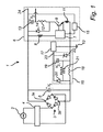
図1は、電源2に接続されるスイッチモード電源デバイス1の概略回路図を図示する。電源2は、スイッチモード電源デバイス1にAC入力電圧を供給するAC電源である。一例として、電源2は、100V及び240V間の振幅及び50Hz乃至60Hzの周波数を持つAC入力電圧を供給する主電源(mains electricity supply)である。電源2は、電磁干渉フィルタ等のフィルタ4を典型的には介して、整流器3に接続される。フィルタ4は、電源2からのノイズを減らす助けになり、これにより、スイッチモード電源デバイス1内のセンシティブな構成要素を保護する。整流器3は、ダイオードブリッジ整流器、とりわけ、全波整流ダイオードブリッジ整流器である。しかしながら、半波整流も適用可能な代替例である。整流器3は、正端子3a及び負端子3bを持ち、正端子3a及び負端子3b間の電位差は、DC入力電圧V1である。スイッチモード電源デバイスはさらに、入力コンデンサ5を有する。入力コンデンサ5は、正端子3aを介しDC入力電圧V1の正極に接続され、負端子3bを介しDC入力電圧V1の負極に接続される。入力コンデンサ5のキャパシタンスは、例えば、約1μF乃至約100μFの範囲内であってもよい。DC入力電圧V1は、リップルを持ち、該リップルは、入力コンデンサ5により平滑化される。他の実施形態によれば、スイッチモード電源デバイス1は、DC入力電圧を供給する電源2に接続されることが目的とされ、この場合、整流器3は省かれる。
FIG. 1 illustrates a schematic circuit diagram of a switch mode power supply device 1 connected to a power supply 2. The power supply 2 is an AC power supply that supplies an AC input voltage to the switch mode power supply device 1. As an example, the power source 2 is a mains electricity supply that supplies an AC input voltage having an amplitude between 100V and 240V and a frequency of 50 Hz to 60 Hz. The power source 2 is connected to the
スイッチモード電源デバイス1は、DC入力電圧V1を受け、電子機器、例えば、ランプ又はコンピュータを給電するためのDC出力電圧V2を供給するよう構成される主回路6を持つ。出力電圧V2の値は、目的とされるアプリケーションに依存するが、典型的には、約20V乃至約140Vの範囲内である。斯くして、主回路6は、バックコンバータ又はブーストコンバータ等のDC/DCコンバータとして動作してもよい。主回路6は、コントローラ7、例えば、パルス幅変調コントローラを持つ。コントローラ7は、正端子3aに接続される。コントローラ7は、スタートアップ抵抗8を介して正端子3aに接続される。ゆえに、スタートアップ抵抗8は、コントローラ7に接続され、DC入力電圧V1の正極に接続される。スタートアップ抵抗8の抵抗は、例えば、約100kΩ乃至約1MΩの範囲内であってもよい。他の実施形態によれば、スタートアップ抵抗8は省かれる。
Switch mode power supply device 1 receives a DC input voltage V 1, with electronic devices, for example, the configured
コントローラ7は、スイッチング素子9に接続される。コントローラ7は、導通状態及び非導通状態間でスイッチング素子9を切換えるよう構成される。この実施形態において、スイッチング素子9は、トランジスタである。スイッチング素子9は、PNPトランジスタ又はNPNトランジスタ等のバイポーラトランジスタであってもよい。スイッチング素子9は、MOSFET等の電界効果トランジスタであってもよい。スイッチング素子9は、サイリスタ、ゲートターンオフサイリスタ(GTO)又は絶縁ゲートバイポーラトランジスタ(IGBT)等であってもよい。スイッチング素子9は、接地電位10にパルス直流を供給するよう構成される。スイッチング素子9は、電流測定用の検知抵抗11を介して接地電位10に接続されてもよい。検知抵抗11は、スイッチング素子9のエミッタに接続され、典型的には、約100mΩ以上の抵抗を持つ。スイッチング素子9は、インダクタの形態のインダクタ素子12に接続される。より正確には、インダクタ素子12は、シングルコイルを有するインダクタである。インダクタ素子12は、スイッチング素子9のコレクタに接続される。インダクタ素子12のインダクタは、例えば、約200μH乃至約10mHの範囲内であってもよい。インダクタ素子12は、エネルギを保存することによりDC出力電圧V2を供給する。DC出力電圧V2は、出力電圧V2を生成するスイッチングサイクル毎に主回路6の出力部に伝達される。
The controller 7 is connected to the switching element 9. The controller 7 is configured to switch the switching element 9 between a conductive state and a non-conductive state. In this embodiment, the switching element 9 is a transistor. The switching element 9 may be a bipolar transistor such as a PNP transistor or an NPN transistor. The switching element 9 may be a field effect transistor such as a MOSFET. The switching element 9 may be a thyristor, a gate turn-off thyristor (GTO), an insulated gate bipolar transistor (IGBT), or the like. The switching element 9 is configured to supply a pulsed direct current to the
主回路6は、典型的には、他の構成要素も含む。図1に示される実施形態によれば、インダクタ素子12は、インダクタ素子12と直列に接続される出力コンデンサ13を介して正端子3aに接続される。DC出力電圧V2は、出力コンデンサ13間の電圧である。主回路6は、出力電圧V2を外部負荷に接続するための出力端子24を備える。ブロッキングダイオード14が、出力コンデンサ13及びインダクタ素子12と並列に接続される。ブロッキングダイオード14は、出力コンデンサ13が、スイッチモード電源デバイス1の動作中スイッチング素子9に放電するのを防止する。DC出力電圧V2をモニタするためのフィードバック回路15が、コントローラ7に接続される。フィードバック回路15は、例えば、DC出力電圧V2が、基準電圧から所定の値を超えてずれた場合にコントローラ7に信号を送るよう構成されてもよい。フィードバック回路15は、あり得る代替例では省かれる。
The
スイッチモード電源デバイス1は、補助電圧V3を供給するよう構成される補助回路16を持つ。補助電圧V3は、典型的には、一定の大きさ又は実質的に一定の大きさを持つDC電圧である。補助電圧V3は、例えば、約5V乃至約12Vの範囲内であってもよい。補助電圧V3は、1つ以上の補助出力端子23を介して負荷17に供給される。負荷17は、接地電位10、すなわち、主回路6と同じ接地電位に接続される。しかしながら、一般には、負荷17は、必ずしも主回路6と同じ接地電位に接続される必要はない。典型的な負荷17の例は、制御回路、マイクロプロセッサ、光電子センサ、パッシブ赤外線センサ又は発光ダイオードを駆動するためのコントローラである。負荷17は、スイッチモード電源デバイス1の構成要素であってもよい。例えば、主回路6は、補助電圧V3がコントローラ7を駆動するように補助電圧V3に接続されてもよい。代替的に、負荷17は、スイッチモード電源デバイス1外にある。すなわち、負荷17は、スイッチモード電源デバイス1に含まれない回路の部分を形成してもよい。
Switch mode power supply device 1 has an
補助回路16は、スイッチング素子9により生成されるパルス直流を受けるよう接続される補助インダクタ18を持つ。補助インダクタ18のインダクタンスは、通例、インダクタ素子のインダクタンスよりかなり小さい。ある実施形態によれば、補助インダクタ18のインダクタンスは、約10μH乃至約500mHの範囲内である。補助インダクタ18及びインダクタ素子12は、互いに磁気的に絶縁される、すなわち、補助インダクタ18及びインダクタ素子12は、結合されない(uncouple)。補助インダクタ18は、補助回路16及び主回路6が共通接地電位に接続されるように接地電位10及び負端子3bに接続される。
The
補助回路16は、接地電位10に接続されるコンデンサ19を持つ。補助電圧V3は、コンデンサ19間の電圧である。補助回路16はまた、補助インダクタ18及びコンデンサ19に接続されるダイオード20を有する。ダイオード20は、半導体ダイオードであってもよい。補助回路16は、補助インダクタ18と並列に接続されるダンピング抵抗21を持つ。補助電圧V3を制限するためのツェナーダイオード22が、コンデンサ19と並列に接続される。補助回路16の他の実施形態は、ダンピング抵抗21及び/又はツェナーダイオード22を含まない。
The
図2は、図1のスイッチモード電源デバイス1と類似のスイッチモード電源デバイス1の概略回路図を図示する。しかしながら、この例においては、インダクタ素子12が、2つの磁気的に結合されるワイヤコイルを持つ変圧器である。
FIG. 2 illustrates a schematic circuit diagram of a switch mode power supply device 1 similar to the switch mode power supply device 1 of FIG. However, in this example, the
図3は、矢印により指示される電流フローを示すスイッチモード電源デバイス1の概略回路図である。スイッチモード電源デバイス1の動作中、DC入力電圧V1が入力コンデンサ5間に印加される結果、入力電流I1が、入力コンデンサ5の正極側から主回路6に流れる。これにより、コントローラ7は、導通状態及び非導通状態間でスイッチング素子9を切換え始める。スタートアップ抵抗8が、コントローラ7の始動を助けてもよい。スイッチングの結果、パルス直流I2が、スイッチング素子9から接地電位10及び補助インダクタ18に流れる。スイッチング素子9が導通状態にある場合、補助インダクタ18は、パルス直流I2によりチャージされる。スイッチング素子9の非導通状態へのスイッチングの結果、パルス直流I2の振幅の減少が生じる。これにより、誘導電流I3が生成される。誘導電流I3は、補助回路16内でダイオード20を通ってコンデンサ19に流れ、コンデンサ19が充電される。コンデンサ19に供給される充電量は、補助インダクタ18のインダクタンス、出力電流I2の強さ及びスイッチング素子9のスイッチング周波数に依存する。ダイオード20は、スイッチング素子9が導通状態に戻された場合にコンデンサ19が放電するのを防止する。スイッチングプロセスの結果、補助電圧V3が、コンデンサ19間に生成される。
FIG. 3 is a schematic circuit diagram of the switch mode power supply device 1 showing a current flow indicated by an arrow. During operation of the switch mode power supply device 1, as a result of the DC input voltage V 1 being applied across the input capacitor 5, the input current I 1 flows from the positive side of the input capacitor 5 to the
当業者は、本発明は、上述の好ましい実施形態に決して限定されないことを認識する。反対に、多くの修正及び変形が、添付の特許請求の範囲の範囲内で可能である。例えば、同じ実施形態によれば、主回路6及び補助回路16は、共通接地電位に接続されない。この場合、レベルシフターの使用が必要かもしれない。
The person skilled in the art realizes that the present invention by no means is limited to the preferred embodiments described above. On the contrary, many modifications and variations are possible within the scope of the appended claims. For example, according to the same embodiment, the
さらに、開示された実施形態に対するバリエーションが、図面、開示及び添付の特許請求の範囲の研究から、当業者によって理解され、実施され得る。請求項において、"有する"という用語は他の要素又はステップを除外するものではなく、単数表記は複数を除外するものではない。特定の手段が相互に異なる従属請求項に記載されるという単なる事実は、これらの手段の組み合わせが有効に用いられ得ないことを示すものではない。
Moreover, variations on the disclosed embodiments can be understood and implemented by those skilled in the art from a study of the drawings, the disclosure, and the appended claims. In the claims, the term “comprising” does not exclude other elements or steps, and the singular does not exclude a plurality. The mere fact that certain measures are recited in mutually different dependent claims does not indicate that a combination of these measured cannot be used to advantage.
Claims (10)
前記DC出力電圧を供給するためのインダクタ素子、
前記インダクタ素子に接続されるスイッチング素子、及び
導通状態及び非導通状態間で前記スイッチング素子を切換えるよう構成されるコントローラ、
を有する主回路、及び
補助電圧を供給するよう構成される補助回路であって、補助インダクタを有する、補助回路、
を有するスイッチモード電源デバイスであって、
前記スイッチング素子は、接地電位にパルス直流を供給するよう構成され、
前記補助インダクタは、前記パルス直流を受けるよう接続され、前記インダクタ素子から磁気的に絶縁される、スイッチモード電源デバイス。 A main circuit configured to receive a DC input voltage and supply a DC output voltage,
An inductor element for supplying the DC output voltage;
A switching element connected to the inductor element, and a controller configured to switch the switching element between a conductive state and a non-conductive state;
An auxiliary circuit configured to supply an auxiliary voltage, the auxiliary circuit having an auxiliary inductor,
A switch mode power supply device comprising:
The switching element is configured to supply a pulsed direct current to a ground potential;
The switch mode power supply device, wherein the auxiliary inductor is connected to receive the pulsed direct current and is magnetically isolated from the inductor element.
前記接地電位に接続されるコンデンサ、及び
前記補助インダクタ及び前記コンデンサに接続されるダイオード
を有し、
前記補助電圧は、前記コンデンサ間の電圧である、請求項2に記載のスイッチモード電源デバイス。 The auxiliary circuit further includes
A capacitor connected to the ground potential; and a diode connected to the auxiliary inductor and the capacitor;
The switch mode power supply device according to claim 2, wherein the auxiliary voltage is a voltage between the capacitors.
The switch mode power supply device according to any one of claims 1 to 8, wherein the auxiliary voltage is configured to be connected to a load outside the switch mode power supply device.
Applications Claiming Priority (3)
| Application Number | Priority Date | Filing Date | Title |
|---|---|---|---|
| EP14180185.2 | 2014-08-07 | ||
| EP14180185 | 2014-08-07 | ||
| PCT/EP2015/067357 WO2016020235A2 (en) | 2014-08-07 | 2015-07-29 | Switch-mode power supply |
Publications (2)
| Publication Number | Publication Date |
|---|---|
| JP2017524328A true JP2017524328A (en) | 2017-08-24 |
| JP2017524328A5 JP2017524328A5 (en) | 2018-09-06 |
Family
ID=51266216
Family Applications (1)
| Application Number | Title | Priority Date | Filing Date |
|---|---|---|---|
| JP2017506783A Pending JP2017524328A (en) | 2014-08-07 | 2015-07-29 | Switch mode power supply |
Country Status (6)
| Country | Link |
|---|---|
| US (1) | US20170229970A1 (en) |
| EP (1) | EP3178157A2 (en) |
| JP (1) | JP2017524328A (en) |
| CN (1) | CN106664013A (en) |
| RU (1) | RU2687055C2 (en) |
| WO (1) | WO2016020235A2 (en) |
Families Citing this family (1)
| Publication number | Priority date | Publication date | Assignee | Title |
|---|---|---|---|---|
| US10523042B2 (en) | 2017-05-12 | 2019-12-31 | Qualcomm Incorporated | Master-slave charging circuit with slave charger input current sensing and adaptive battery current limiting |
Family Cites Families (9)
| Publication number | Priority date | Publication date | Assignee | Title |
|---|---|---|---|---|
| JPH08182309A (en) * | 1994-12-22 | 1996-07-12 | Hitachi Lighting Ltd | Chopper |
| RU2095927C1 (en) * | 1995-02-17 | 1997-11-10 | Андрей Васильевич Щукин | Commutator for direct voltage converter |
| WO2001018946A1 (en) * | 1999-09-03 | 2001-03-15 | Lambda Electronics | Inductor current sensing |
| JP2005051845A (en) * | 2003-07-30 | 2005-02-24 | Ushio Inc | Dc-dc converter and high-pressure discharge lamp lighting device using it |
| EP1807925A1 (en) * | 2004-10-28 | 2007-07-18 | Koninklijke Philips Electronics N.V. | Ultra low power stand-by supply |
| CN201022180Y (en) * | 2006-11-28 | 2008-02-13 | 尼克森微电子股份有限公司 | First side feedback controlled exchange power supplier |
| US8198874B2 (en) * | 2009-06-30 | 2012-06-12 | Cirrus Logic, Inc. | Switching power converter with current sensing transformer auxiliary power supply |
| US20140119058A1 (en) * | 2012-10-30 | 2014-05-01 | Chicony Power Technology Co., Ltd. | Power voltage conversion system for controller integrated circuit |
| US9735663B2 (en) * | 2013-02-20 | 2017-08-15 | Power Integrations, Inc. | BJT drive scheme |
-
2015
- 2015-07-29 EP EP15744201.3A patent/EP3178157A2/en not_active Withdrawn
- 2015-07-29 JP JP2017506783A patent/JP2017524328A/en active Pending
- 2015-07-29 WO PCT/EP2015/067357 patent/WO2016020235A2/en active Application Filing
- 2015-07-29 CN CN201580042430.2A patent/CN106664013A/en active Pending
- 2015-07-29 US US15/501,876 patent/US20170229970A1/en not_active Abandoned
- 2015-07-29 RU RU2017107189A patent/RU2687055C2/en not_active IP Right Cessation
Also Published As
| Publication number | Publication date |
|---|---|
| WO2016020235A3 (en) | 2016-03-31 |
| CN106664013A (en) | 2017-05-10 |
| EP3178157A2 (en) | 2017-06-14 |
| US20170229970A1 (en) | 2017-08-10 |
| RU2017107189A (en) | 2018-09-07 |
| RU2017107189A3 (en) | 2019-03-05 |
| WO2016020235A2 (en) | 2016-02-11 |
| RU2687055C2 (en) | 2019-05-07 |
Similar Documents
| Publication | Publication Date | Title |
|---|---|---|
| TWI501533B (en) | An off-line voltage regulator, off-line regulator integrated circuit and voltage convert method thereof | |
| US11095209B2 (en) | Power supply control circuit, power supply device and electronic apparatus | |
| JP6456832B2 (en) | Driving apparatus and driving method for driving load | |
| JP6403042B2 (en) | Power supply apparatus and lighting apparatus using the same | |
| TWI445297B (en) | Power supply | |
| JP5761301B2 (en) | Lighting device and lighting apparatus | |
| TWI701442B (en) | Primary side constant current regulation | |
| US20130334893A1 (en) | Power transmission system and power transmitting apparatus | |
| JP2016158398A (en) | Semiconductor device for power supply control | |
| JP6271175B2 (en) | AC / DC converter and its control circuit, power adapter and electronic device | |
| US9723666B2 (en) | Lighting device and lighting fixture using same | |
| TW201434349A (en) | LED driver | |
| JP5324009B2 (en) | Power receiving device and non-contact power transmission system using the same | |
| JP2015139258A (en) | Switching power supply device | |
| JP2014143776A (en) | Wireless power receiving device, wireless power transmitting device and wireless power feeding device | |
| JP6035282B2 (en) | Inductive power transmission device | |
| JP2015023608A (en) | Ac-dc converter and control circuit thereof, power adapter, and electronic apparatus | |
| JP5417885B2 (en) | Power supply | |
| JP2017524328A (en) | Switch mode power supply | |
| WO2015019908A1 (en) | Wireless power transmission system | |
| EP3029471A1 (en) | A switched mode power supply circuit | |
| JP5478347B2 (en) | Light source lighting device and lighting fixture | |
| JP2013251528A (en) | Light-emitting diode drive circuit | |
| KR101739755B1 (en) | LED driving circuit | |
| JP2019164922A (en) | Lighting device, and emergency luminaire |
Legal Events
| Date | Code | Title | Description |
|---|---|---|---|
| RD02 | Notification of acceptance of power of attorney |
Free format text: JAPANESE INTERMEDIATE CODE: A7422 Effective date: 20170515 |
|
| RD04 | Notification of resignation of power of attorney |
Free format text: JAPANESE INTERMEDIATE CODE: A7424 Effective date: 20170609 |
|
| A521 | Request for written amendment filed |
Free format text: JAPANESE INTERMEDIATE CODE: A523 Effective date: 20180727 |
|
| A621 | Written request for application examination |
Free format text: JAPANESE INTERMEDIATE CODE: A621 Effective date: 20180727 |
|
| A521 | Request for written amendment filed |
Free format text: JAPANESE INTERMEDIATE CODE: A523 Effective date: 20180906 |
|
| A977 | Report on retrieval |
Free format text: JAPANESE INTERMEDIATE CODE: A971007 Effective date: 20190424 |
|
| A131 | Notification of reasons for refusal |
Free format text: JAPANESE INTERMEDIATE CODE: A131 Effective date: 20190507 |
|
| A02 | Decision of refusal |
Free format text: JAPANESE INTERMEDIATE CODE: A02 Effective date: 20190822 |