JP5478347B2 - Light source lighting device and lighting fixture - Google Patents
Light source lighting device and lighting fixture Download PDFInfo
- Publication number
- JP5478347B2 JP5478347B2 JP2010094434A JP2010094434A JP5478347B2 JP 5478347 B2 JP5478347 B2 JP 5478347B2 JP 2010094434 A JP2010094434 A JP 2010094434A JP 2010094434 A JP2010094434 A JP 2010094434A JP 5478347 B2 JP5478347 B2 JP 5478347B2
- Authority
- JP
- Japan
- Prior art keywords
- voltage
- overvoltage
- switching element
- light source
- zener diode
- Prior art date
- Legal status (The legal status is an assumption and is not a legal conclusion. Google has not performed a legal analysis and makes no representation as to the accuracy of the status listed.)
- Active
Links
- 239000003990 capacitor Substances 0.000 claims description 39
- 238000009499 grossing Methods 0.000 claims description 30
- 238000001514 detection method Methods 0.000 claims description 25
- 230000001960 triggered effect Effects 0.000 claims description 3
- 230000005669 field effect Effects 0.000 claims 3
- 238000004804 winding Methods 0.000 description 5
- 238000010586 diagram Methods 0.000 description 4
- 230000007423 decrease Effects 0.000 description 1
- 238000012544 monitoring process Methods 0.000 description 1
Images

Landscapes
- Circuit Arrangement For Electric Light Sources In General (AREA)
- Led Devices (AREA)
Description
この発明は光源を点灯させる光源点灯装置に関する。 The present invention relates to a light source lighting device for lighting a light source.
LED照明装置(例えば特許文献1、2)は、LEDが点灯中にLEDのオープン故障が発生した場合や、LEDが取り外された場合には、2次側整流回路、2次側平滑コンデンサの印加電圧が上昇する。2次側整流回路、2次側平滑コンデンサに過大な電圧が印加されると2次側整流回路、2次側平滑コンデンサが故障し、電源基板の交換が必要となる。
LED lighting devices (for example,
この発明は、LEDのオープン故障や、LEDの取り外しに際して、2次側平滑コンデンサの電圧上昇を簡易な構成で防止可能な点灯装置の提供を目的とする。 An object of the present invention is to provide a lighting device that can prevent an open failure of an LED or a voltage increase of a secondary smoothing capacitor with a simple configuration when the LED is removed.
この発明の光源点灯装置は、スイッチング素子と、所定の動作電圧で動作し、前記スイッチング素子のスイッチングを制御するスイッチング素子制御部と、前記スイッチング素子がスイッチングすることによって生成される直流電圧に基づく電荷を充電し、充電された電荷に基づく直流の充電電圧を光源に供給する供給コンデンサとを備えた光源用直流電圧生成部と、前記供給コンデンサの前記充電電圧を監視し、前記充電電圧が過電圧として設定された設定値以上になると過電圧検出信号を出力する過電圧検出部と、所定の電圧が印加されて動作すると共に前記スイッチング素子制御部の動作電圧でも動作し、前記スイッチング素子制御部の動作電圧よりも低く、かつ、前記スイッチング素子制御部の動作しない低電圧でも動作する過電圧発生記憶部であって、前記過電圧検出部から前記過電圧検出信号を入力し、前記過電圧検出信号の入力を契機として前記供給コンデンサの過電圧発生を記憶し、前記過電圧発生の記憶に伴い継続してラッチ信号を出力する過電圧発生記憶部と、前記スイッチング素子制御部と前記過電圧発生記憶部とを動作させる電圧を出力する制御電源部とを備え、前記スイッチング素子制御部と前記過電圧発生記憶部とは、前記制御電源部に対して並列接続し、前記制御電源部は、前記過電圧発生記憶部から前記ラッチ信号を入力し、前記ラッチ信号の入力が継続しているときは前記スイッチング素子制御部が動作せず、かつ、前記過電圧発生記憶部が動作する前記低電圧を出力することを特徴とする。 The light source lighting device according to the present invention includes a switching element, a switching element control unit that operates at a predetermined operating voltage and controls switching of the switching element, and a charge based on a DC voltage generated by switching of the switching element. A light source DC voltage generator comprising a supply capacitor for supplying a DC charging voltage based on the charged charge to the light source, and monitoring the charging voltage of the supply capacitor, wherein the charging voltage is overvoltage An overvoltage detection unit that outputs an overvoltage detection signal when the set value is exceeded, and operates with a predetermined voltage applied and also operates with the operating voltage of the switching element control unit. From the operating voltage of the switching element control unit Overvoltage that is low and operates even at low voltage where the switching element controller does not operate The raw storage unit receives the overvoltage detection signal from the overvoltage detection unit, stores the overvoltage generation of the supply capacitor triggered by the input of the overvoltage detection signal, and continuously latches with the storage of the overvoltage generation An overvoltage generation storage unit that outputs a signal, and a control power supply unit that outputs a voltage for operating the switching element control unit and the overvoltage generation storage unit, the switching element control unit and the overvoltage generation storage unit, The control power supply unit is connected in parallel to the control power supply unit, and the control power supply unit inputs the latch signal from the overvoltage generation storage unit, and the switching element control unit operates when the input of the latch signal is continued. And the low voltage at which the overvoltage generation storage unit operates is output.
本発明の光源点灯装置によれば、LEDがオープン故障したり、LEDが外されたりした場合でも、2次側平滑コンデンサに過大な電圧が発生することを簡易な構成で防止するLED点灯装置を提供できる。 According to the light source lighting device of the present invention, an LED lighting device that prevents an excessive voltage from being generated in the secondary-side smoothing capacitor with a simple configuration even when the LED fails to open or is removed. Can be provided.
実施の形態1.
図1、図2を参照して実施の形態1を説明する。
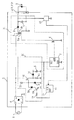
図1は、実施の形態1のLED点灯装置2(光源点灯装置)の構成図である。LED点灯装置2は、整流回路4、DC−DCコンバータ21(光源用直流電圧生成部)、過電圧検出回路16(過電圧検出部)、ラッチ回路17(過電圧発生記憶部)、制御電源部30を備えている。
The first embodiment will be described with reference to FIGS.
FIG. 1 is a configuration diagram of an LED lighting device 2 (light source lighting device) according to the first embodiment. The
(DC−DCコンバータ21)
DC−DCコンバータ21は、トランス5(1次側)、第1のトランジスタ6(スイッチング素子)が直列接続されている。制御回路7(スイッチング素子制御部)は第1のトランジスタ6であるスイッチング素子を制御する。制御回路7は、平滑コンデンサ15を介して動作電圧の供給を受ける。商用交流電源1の交流電圧は、整流回路4で直流に変換され、DC−DCコンバータ21に入力され、入力時よりも低い直流電圧に変換される。DC−DCコンバータ21内では、整流回路4の出力電圧が、トランス5、第1のトランジスタ6からなる直列回路に印加される。第1のトランジスタ6は制御回路7からの出力で制御されることにより、その出力に応じて高周波数でスイッチングする。トランス5の2次側回路は、2次側整流ダイオード8と2次側平滑コンデンサ9(供給コンデンサ)が接続される。第1のトランジスタ6がONしているとき、整流回路4の電圧がトランス5の1次巻き線5aに印加され、2次巻き線5bには巻き数比に比例した電圧が誘起される。この電圧の極性は、2次側整流ダイオード8を正方向にバイアスし、2次側平滑コンデンサ9を充電するように流れる。2次側平滑コンデンサ9に充電された電荷に基づく充電電圧がLED3に供給される。
(DC-DC converter 21)
In the DC-
(過電圧検出回路16)
過電圧検出回路16は、2次側平滑コンデンサ9の充電電圧を監視し、充電電圧が過電圧として設定された設定値以上(図2(3)のVs以上)になると過電圧検出信号を出力する。
(Overvoltage detection circuit 16)
The
(ラッチ回路17)
ラッチ回路17は、制御電源部30から所定の電圧が印加されて動作する。図1に示すようにラッチ回路17と制御回路7とは、制御電源部30に対して、並列接続である。
ラッチ回路17は、制御回路7の動作電圧でも動作し、また、制御回路7の動作電圧よりも低く、かつ、制御回路7の動作しない低電圧でも動作する。ラッチ回路17は、後述のように過電圧検出回路16から過電圧検出信号を入力し、過電圧検出信号の入力を契機として2次側平滑コンデンサ9の過電圧発生を記憶し、過電圧発生の記憶に伴い継続して信号を出力する。
(Latch circuit 17)
The
The
(制御電源部30)
制御電源部30は制御回路7とラッチ回路17とを動作させる電圧を平滑コンデンサ15から出力する。後述の動作説明で述べるが、制御電源部30は、ラッチ回路17から信号を入力し、この信号の入力が継続しているときは、「制御回路7が動作せず、かつラッチ回路17が動作する低電圧」を出力する。制御電源部30は、第2のトランジスタ(第2のスイッチング素子)10としてMOS−FET(nチャネル形)を用いている。「第2のスイッチング素子10、抵抗11(第1抵抗)」の直列回路と、「抵抗12(第2抵抗)、第1のツェナーダイオード13」の直列回路とが整流回路4に対して、並列に接続している。「抵抗12、第1のツェナーダイオード13」の直列回路の方が整流回路4側である。 第2のツェナーダイオード20のカソード側が抵抗12と第1のツェナーダイオード13との中間点に接続し、アノード側がトランジスタ19のコレクタ側に接続している。トランジスタ19はエミッタ接地であり、ベース抵抗18を介して、ラッチ回路17の出力端子に接続している。また、第2のスイッチング素子10のゲートが抵抗12と第1のツェナーダイオード13との中間点に接続している。第2のスイッチング素子10のソースと抵抗11との中間点にはダイオード14のアノード側が接続され、カソード側には平滑コンデンサ15が直列接続される。ダイオード14と平滑コンデンサ15との中間点はラッチ回路17と制御回路7とのVCC(電源入力)に接続する。
(Control power supply unit 30)
The control
(動作の説明)
次に図2の波形図を参照してLED点灯装置2の動作を説明する。
図2の横軸は時間を示す。
図2(1)は、平滑コンデンサ15の電圧を示す。
図2(2)は、制御回路7の出力電圧を示す。
図2(3)は、2次側平滑コンデンサ9の電圧波形を示す。
図2(4)は、過電圧検出回路16の出力電圧を示す。
図2(5)は、ラッチ回路17の過電圧発生の記憶状態を示す。
(Description of operation)
Next, the operation of the
The horizontal axis in FIG. 2 indicates time.
FIG. 2 (1) shows the voltage of the smoothing capacitor 15.
FIG. 2 (2) shows the output voltage of the
FIG. 2 (3) shows the voltage waveform of the secondary
FIG. 2 (4) shows the output voltage of the
FIG. 2 (5) shows the storage state of the overvoltage occurrence of the
商用電源1からの電圧は整流回路4で整流され、「トランス5、第1のトランジスタ6」の直列回路に印加されると共に、「第2のトランジスタ10、抵抗11」の直列回路、「抵抗12、第1のツェナーダイオード13」の直列回路に印加される。抵抗11には第1のツェナーダイオード13のツェナー電圧でクリップされた電圧が発生し、この電圧はダイオード14を介して平滑コンデンサ15で平滑される。図1に示すように、平滑コンデンサ15からの平滑電圧は、制御回路7のVCC(電源)及びラッチ回路17のVCC(電源)に接続されている。
The voltage from the
図2(1)は、平滑コンデンサ15の電圧を示すが、時刻T1のタイミングで、平滑コンデンサ15の電圧が第1のツェナーダイオード13のツェナー電圧から第2のツェナーダイオード20のツェナー電圧に切り替わったことを示している。時刻T1は、過電圧検出回路16が2次側平滑コンデンサ9の過電圧を検出した時刻である。
FIG. 2 (1) shows the voltage of the smoothing capacitor 15. At the time T1, the voltage of the smoothing capacitor 15 is switched from the Zener voltage of the
図2(2)に示すように、時刻T1以前では、制御回路7はOUT端子から高周波電圧を出力し、第1のトランジスタ6を駆動する。第1のトランジスタ6の駆動によりトランス5の1次巻き線5aに高周波電圧が発生し、2次巻き線5bには巻き数に対応した電圧が出力される。トランス5の2次巻き線5bからの出力は2次側整流ダイオード8で整流された後、2次側平滑コンデンサ9で平滑されてLED3に直流電流を流し、LED3が点灯する。
As shown in FIG. 2B, before the time T1, the
図2(3)は2次側平滑コンデンサ9の電圧波形を示す。例えばA点でLED3がLED点灯装置2から外された場合、2次側平滑コンデンサ9の電圧が上昇する。2次側平滑コンデンサ9の電圧が所定電圧Vsを超えると、図2(4)に示すように、過電圧検出回路16がラッチ回路17に過電圧を超えた信号(過電圧検出信号)を送出する。ラッチ回路17は過電圧検出回路16から過電圧検出信号を入力し、過電圧発生を記憶する(図2(5)の時刻T1以降)。
FIG. 2 (3) shows the voltage waveform of the secondary
ラッチ回路17が過電圧発生を記憶すると、ラッチ回路17は、図2(5)に示すように、ラッチ回路17の出力(OUT端子)からベース抵抗18を介して、トランジスタ19にベース電流(信号)を流し、トランジスタ19はONとなる。
When the
トランジスタ19がONになれば第2のツェナーダイオード20に電流が流れるが、第1のツェナーダイオード13のツェナー電圧V1(第1ツェナー)>第2のツェナーダイオード20のツェナー電圧V2(第2ツェナー)となる関係に設定している。
すなわち、
V1(第1ツェナー)>V2(第2ツェナー)
である。
このため、図2(1)のB点よりも制御回路7のVCC(電源)が低くなる。すなわち制御回路7のVCCは時刻T1を境界として第1のツェナーダイオード13の電圧から第2のツェナーダイオード20の電圧へと低下する。なお、ラッチ回路17に印加される電圧は制御回路7に印加される電圧と同じである。第2のツェナーダイオード20の電圧は制御回路7の動作電圧よりも低く、かつ、ラッチ回路17の動作する電圧になるように設定してある。ラッチ回路17のVCC(電源)は平滑コンデンサ15に接続されているのでラッチ回路17は低い電圧(V2(第2ツェナー))でも動作(記憶)する。一方、制御回路7は一般に低電圧検出回路が内蔵され、所定の電源電圧(V2(第2ツェナー))では動作が停止する。このように、第2のツェナーダイオード20のツェナー電圧は、保護ラッチ回路17を動作させ、かつ、制御回路7に対しては低電圧ロックがかかる電圧に選定される。
When the
That is,
V1 (first Zener)> V2 (second Zener)
It is.
For this reason, the VCC (power supply) of the
以上の実施の形態1ではLED点灯装置2を説明したが、LED以外の光源を使用する点灯装置に適用しても構わない。また、実施の形態1のLED(光源)点灯装置を備えた照明器具の実施形態とすることも、もちろん可能である。
Although the
実施の形態1のLED点灯装置2によれば、LEDがオープン故障したり、LEDが外されたりした場合でも、2次側平滑コンデンサに過大な電圧が発生することを簡易な構成で防止するLED点灯装置を提供できる。
According to the
1 商用電源、2 LED点灯装置、21 DC−DCコンバータ、3 LED、4 整流回路、5 トランス、6 第1のトランジスタ、7 制御回路、8 2次側整流ダイオード、9 2次側平滑コンデンサ、10 第2のトランジスタ、11 抵抗、12 抵抗、13 第1のツェナーダイオード、14 ダイオード、15 平滑コンデンサ、16 過電圧検出回路、17 ラッチ回路、18 ベース抵抗、19 トランジスタ、20 第2のツェナーダイオード、30 制御電源部。
DESCRIPTION OF
Claims (3)
前記供給コンデンサの前記充電電圧を監視し、前記充電電圧が過電圧として設定された設定値以上になると過電圧検出信号を出力する過電圧検出部と、
所定の電圧が印加されて動作すると共に前記スイッチング素子制御部の動作電圧でも動作し、前記スイッチング素子制御部の動作電圧よりも低く、かつ、前記スイッチング素子制御部の動作しない低電圧でも動作する過電圧発生記憶部であって、前記過電圧検出部から前記過電圧検出信号を入力し、前記過電圧検出信号の入力を契機として前記供給コンデンサの過電圧発生を記憶し、前記過電圧発生の記憶に伴い継続してラッチ信号を出力する過電圧発生記憶部と、
前記スイッチング素子制御部と前記過電圧発生記憶部とを動作させる電圧を出力する制御電源部と
を備え、
前記スイッチング素子制御部と前記過電圧発生記憶部とは、
前記制御電源部に対して並列接続し、
前記制御電源部は、
前記過電圧発生記憶部から前記ラッチ信号を入力し、前記ラッチ信号の入力が継続しているときは前記スイッチング素子制御部が動作せず、かつ、前記過電圧発生記憶部が動作する前記低電圧を出力することを特徴とする光源点灯装置。 A switching element, a switching element control unit that operates at a predetermined operating voltage and controls switching of the switching element, and a charge based on a DC voltage generated by switching of the switching element, and the charged charge A direct-current voltage generator for a light source comprising a supply capacitor for supplying a direct-current charging voltage to the light source,
An overvoltage detector that monitors the charging voltage of the supply capacitor and outputs an overvoltage detection signal when the charging voltage is equal to or higher than a set value set as an overvoltage;
An overvoltage that operates with a predetermined voltage applied, operates with the operating voltage of the switching element control unit, and operates with a low voltage that is lower than the operating voltage of the switching element control unit and does not operate with the switching element control unit A generation storage unit that receives the overvoltage detection signal from the overvoltage detection unit, stores the overvoltage generation of the supply capacitor triggered by the input of the overvoltage detection signal, and continuously latches with the storage of the overvoltage generation An overvoltage generation storage unit for outputting a signal;
A control power supply unit that outputs a voltage for operating the switching element control unit and the overvoltage generation storage unit,
The switching element control unit and the overvoltage generation storage unit are:
Connected in parallel to the control power supply,
The control power supply unit
The latch signal is input from the overvoltage generation storage unit, and when the input of the latch signal is continued, the switching element control unit does not operate and the low voltage at which the overvoltage generation storage unit operates is output. A light source lighting device.
交流電圧を整流する整流回路によって整流された整流電圧を入力し、入力した整流電圧を前記スイッチング素子でスイッチングすることにより前記直流電圧を生成し、
前記制御電源部は、
ドレインが前記整流回路の正極側に接続する電界効果トランジスタと、
前記電界効果トランジスタのソースに直列接続する第1抵抗と平滑コンデンサとの並列接続と、
前記電界効果トランジスタのゲートとソース間に接続された第1ツェナーダイオードと、
一端が前記整流回路の正極側に接続し他端が前記第1ツェナーダイオードのカソード側に接続して前記前記第1ツェナーダイオードに電流を流す第2抵抗と、
前記第1ツェナーダイオードと並列に接続された第2ツェナーダイオードとトランジスタとの直列接続であって、前記第2ツェナーダイオードのカソード側が前記第1ツェナーダイオードのカソード側に接続し、前記トランジスタが前記過電圧発生記憶部と接続し前記過電圧発生記憶部からの前記信号の入力によりオンとなる前記第2ツェナーダイオードと前記トランジスタとの直列接続と
を備え、
前記コンデンサのコンデンサ電圧を前記スイッチング素子制御部と前記過電圧発生記憶部とを動作させる動作電圧として出力することを特徴とする請求項1記載の光源点灯装置。 The light source direct voltage generator is
A rectified voltage rectified by a rectifier circuit that rectifies an AC voltage is input, and the DC voltage is generated by switching the input rectified voltage with the switching element,
The control power supply unit
A field effect transistor having a drain connected to the positive side of the rectifier circuit;
A parallel connection of a first resistor and a smoothing capacitor connected in series to the source of the field effect transistor;
A first Zener diode connected between a gate and a source of the field effect transistor;
A second resistor having one end connected to the positive side of the rectifier circuit and the other end connected to the cathode side of the first Zener diode, and flowing a current through the first Zener diode;
A second Zener diode connected in parallel with the first Zener diode and a transistor are connected in series, the cathode side of the second Zener diode is connected to the cathode side of the first Zener diode, and the transistor is connected to the overvoltage. A series connection of the second Zener diode and the transistor connected to the generation storage unit and turned on by the input of the signal from the overvoltage generation storage unit;
2. The light source lighting device according to claim 1, wherein the capacitor voltage of the capacitor is output as an operating voltage for operating the switching element control unit and the overvoltage generation storage unit.
前記光源点灯装置から電力が供給される光源を着脱可能とするコネクタと
を備えることを特徴とする照明器具。 The light source lighting device according to claim 1 or 2,
A luminaire comprising: a connector that allows a light source to be supplied with power from the light source lighting device to be detachable.
Priority Applications (1)
| Application Number | Priority Date | Filing Date | Title |
|---|---|---|---|
| JP2010094434A JP5478347B2 (en) | 2010-04-15 | 2010-04-15 | Light source lighting device and lighting fixture |
Applications Claiming Priority (1)
| Application Number | Priority Date | Filing Date | Title |
|---|---|---|---|
| JP2010094434A JP5478347B2 (en) | 2010-04-15 | 2010-04-15 | Light source lighting device and lighting fixture |
Publications (3)
| Publication Number | Publication Date |
|---|---|
| JP2011228025A JP2011228025A (en) | 2011-11-10 |
| JP2011228025A5 JP2011228025A5 (en) | 2013-05-09 |
| JP5478347B2 true JP5478347B2 (en) | 2014-04-23 |
Family
ID=45043185
Family Applications (1)
| Application Number | Title | Priority Date | Filing Date |
|---|---|---|---|
| JP2010094434A Active JP5478347B2 (en) | 2010-04-15 | 2010-04-15 | Light source lighting device and lighting fixture |
Country Status (1)
| Country | Link |
|---|---|
| JP (1) | JP5478347B2 (en) |
Families Citing this family (2)
| Publication number | Priority date | Publication date | Assignee | Title |
|---|---|---|---|---|
| JP6128304B2 (en) * | 2012-04-26 | 2017-05-17 | 東芝ライテック株式会社 | Emergency lighting device |
| JP6013809B2 (en) * | 2012-07-05 | 2016-10-25 | ローム株式会社 | LED driver circuit and lighting device |
Family Cites Families (4)
| Publication number | Priority date | Publication date | Assignee | Title |
|---|---|---|---|---|
| JP2002262557A (en) * | 2001-02-27 | 2002-09-13 | Fuji Electric Co Ltd | Protection circuit for switching regulator |
| JP4944562B2 (en) * | 2006-10-18 | 2012-06-06 | パナソニック株式会社 | Switching power supply |
| JP2009010100A (en) * | 2007-06-27 | 2009-01-15 | Toshiba Lighting & Technology Corp | Power supply and lighting device |
| JP5237727B2 (en) * | 2008-08-26 | 2013-07-17 | パナソニック株式会社 | LED driving device, lighting device and lighting fixture |
-
2010
- 2010-04-15 JP JP2010094434A patent/JP5478347B2/en active Active
Also Published As
| Publication number | Publication date |
|---|---|
| JP2011228025A (en) | 2011-11-10 |
Similar Documents
| Publication | Publication Date | Title |
|---|---|---|
| JP5632664B2 (en) | Semiconductor light-emitting element lighting device and lighting fixture using the same | |
| JP6122257B2 (en) | DC / DC converter and control circuit thereof, power supply using the same, power adapter, and electronic device | |
| TWI539732B (en) | DC / DC converter and the use of its power supply devices and electronic equipment | |
| US9985543B1 (en) | Switching power supply | |
| JP5554108B2 (en) | Overcurrent prevention type power supply device and lighting fixture using the same | |
| JP6403042B2 (en) | Power supply apparatus and lighting apparatus using the same | |
| JP2008048515A (en) | Switching power supply device | |
| JP2006352975A (en) | Switching power unit | |
| JP2018019589A (en) | Isolation synchronous rectification type dc/dc converter, synchronous rectification controller, shunt regulator circuit, power supply adapter, and electronic device | |
| JP2015084616A (en) | Lighting device and light fixture | |
| JP2014075875A (en) | Dc power supply device | |
| JP2015228720A (en) | Self-excited resonance power factor improvement circuit and light source driver | |
| US9621060B2 (en) | Self-excited power conversion circuit for secondary side control output power | |
| US8467202B2 (en) | Flyback power supply system | |
| JP6187024B2 (en) | LED power supply device and LED lighting device | |
| JP5478347B2 (en) | Light source lighting device and lighting fixture | |
| JP6842252B2 (en) | Insulation synchronous rectification type DC / DC converter, its protection method, power adapter and electronic equipment | |
| JP2017158292A (en) | Power supply unit and illumination device | |
| JP2015126638A (en) | Switching power supply device | |
| CN104349544A (en) | LED driving apparatus and illuminating device | |
| KR200444228Y1 (en) | Switching mode power supply having over voltage protection circuit | |
| JP2017073433A (en) | Led power supply device | |
| JP2017112782A (en) | Switching power supply device | |
| JP2016063603A (en) | Power unit and illumination device | |
| JP6405863B2 (en) | Lighting device |
Legal Events
| Date | Code | Title | Description |
|---|---|---|---|
| A521 | Request for written amendment filed |
Free format text: JAPANESE INTERMEDIATE CODE: A523 Effective date: 20130327 |
|
| A621 | Written request for application examination |
Free format text: JAPANESE INTERMEDIATE CODE: A621 Effective date: 20130327 |
|
| A977 | Report on retrieval |
Free format text: JAPANESE INTERMEDIATE CODE: A971007 Effective date: 20131213 |
|
| TRDD | Decision of grant or rejection written | ||
| A01 | Written decision to grant a patent or to grant a registration (utility model) |
Free format text: JAPANESE INTERMEDIATE CODE: A01 Effective date: 20140114 |
|
| A61 | First payment of annual fees (during grant procedure) |
Free format text: JAPANESE INTERMEDIATE CODE: A61 Effective date: 20140210 |
|
| R150 | Certificate of patent or registration of utility model |
Ref document number: 5478347 Country of ref document: JP Free format text: JAPANESE INTERMEDIATE CODE: R150 |
|
| R250 | Receipt of annual fees |
Free format text: JAPANESE INTERMEDIATE CODE: R250 |
|
| R250 | Receipt of annual fees |
Free format text: JAPANESE INTERMEDIATE CODE: R250 |
|
| R250 | Receipt of annual fees |
Free format text: JAPANESE INTERMEDIATE CODE: R250 |
|
| R250 | Receipt of annual fees |
Free format text: JAPANESE INTERMEDIATE CODE: R250 |
|
| R250 | Receipt of annual fees |
Free format text: JAPANESE INTERMEDIATE CODE: R250 |
|
| R250 | Receipt of annual fees |
Free format text: JAPANESE INTERMEDIATE CODE: R250 |
|
| R250 | Receipt of annual fees |
Free format text: JAPANESE INTERMEDIATE CODE: R250 |
|
| R250 | Receipt of annual fees |
Free format text: JAPANESE INTERMEDIATE CODE: R250 |