JP2017517890A - Corrugated interconnects for foldable and stretchable devices - Google Patents
Corrugated interconnects for foldable and stretchable devices Download PDFInfo
- Publication number
- JP2017517890A JP2017517890A JP2016569605A JP2016569605A JP2017517890A JP 2017517890 A JP2017517890 A JP 2017517890A JP 2016569605 A JP2016569605 A JP 2016569605A JP 2016569605 A JP2016569605 A JP 2016569605A JP 2017517890 A JP2017517890 A JP 2017517890A
- Authority
- JP
- Japan
- Prior art keywords
- interconnect
- flexible substrate
- corrugated
- assembly
- profile
- Prior art date
- Legal status (The legal status is an assumption and is not a legal conclusion. Google has not performed a legal analysis and makes no representation as to the accuracy of the status listed.)
- Pending
Links
Images


Classifications
-
- H—ELECTRICITY
- H05—ELECTRIC TECHNIQUES NOT OTHERWISE PROVIDED FOR
- H05K—PRINTED CIRCUITS; CASINGS OR CONSTRUCTIONAL DETAILS OF ELECTRIC APPARATUS; MANUFACTURE OF ASSEMBLAGES OF ELECTRICAL COMPONENTS
- H05K1/00—Printed circuits
- H05K1/02—Details
- H05K1/0277—Bendability or stretchability details
- H05K1/0283—Stretchable printed circuits
-
- H—ELECTRICITY
- H01—ELECTRIC ELEMENTS
- H01L—SEMICONDUCTOR DEVICES NOT COVERED BY CLASS H10
- H01L21/00—Processes or apparatus adapted for the manufacture or treatment of semiconductor or solid state devices or of parts thereof
- H01L21/02—Manufacture or treatment of semiconductor devices or of parts thereof
- H01L21/04—Manufacture or treatment of semiconductor devices or of parts thereof the devices having at least one potential-jump barrier or surface barrier, e.g. PN junction, depletion layer or carrier concentration layer
- H01L21/48—Manufacture or treatment of parts, e.g. containers, prior to assembly of the devices, using processes not provided for in a single one of the subgroups H01L21/06 - H01L21/326
- H01L21/4814—Conductive parts
- H01L21/4846—Leads on or in insulating or insulated substrates, e.g. metallisation
- H01L21/4853—Connection or disconnection of other leads to or from a metallisation, e.g. pins, wires, bumps
-
- H—ELECTRICITY
- H01—ELECTRIC ELEMENTS
- H01L—SEMICONDUCTOR DEVICES NOT COVERED BY CLASS H10
- H01L21/00—Processes or apparatus adapted for the manufacture or treatment of semiconductor or solid state devices or of parts thereof
- H01L21/02—Manufacture or treatment of semiconductor devices or of parts thereof
- H01L21/04—Manufacture or treatment of semiconductor devices or of parts thereof the devices having at least one potential-jump barrier or surface barrier, e.g. PN junction, depletion layer or carrier concentration layer
- H01L21/48—Manufacture or treatment of parts, e.g. containers, prior to assembly of the devices, using processes not provided for in a single one of the subgroups H01L21/06 - H01L21/326
- H01L21/4814—Conductive parts
- H01L21/4846—Leads on or in insulating or insulated substrates, e.g. metallisation
- H01L21/486—Via connections through the substrate with or without pins
-
- H—ELECTRICITY
- H01—ELECTRIC ELEMENTS
- H01L—SEMICONDUCTOR DEVICES NOT COVERED BY CLASS H10
- H01L21/00—Processes or apparatus adapted for the manufacture or treatment of semiconductor or solid state devices or of parts thereof
- H01L21/02—Manufacture or treatment of semiconductor devices or of parts thereof
- H01L21/04—Manufacture or treatment of semiconductor devices or of parts thereof the devices having at least one potential-jump barrier or surface barrier, e.g. PN junction, depletion layer or carrier concentration layer
- H01L21/50—Assembly of semiconductor devices using processes or apparatus not provided for in a single one of the subgroups H01L21/06 - H01L21/326, e.g. sealing of a cap to a base of a container
- H01L21/56—Encapsulations, e.g. encapsulation layers, coatings
- H01L21/565—Moulds
-
- H—ELECTRICITY
- H01—ELECTRIC ELEMENTS
- H01L—SEMICONDUCTOR DEVICES NOT COVERED BY CLASS H10
- H01L23/00—Details of semiconductor or other solid state devices
- H01L23/28—Encapsulations, e.g. encapsulating layers, coatings, e.g. for protection
- H01L23/31—Encapsulations, e.g. encapsulating layers, coatings, e.g. for protection characterised by the arrangement or shape
- H01L23/3107—Encapsulations, e.g. encapsulating layers, coatings, e.g. for protection characterised by the arrangement or shape the device being completely enclosed
- H01L23/3114—Encapsulations, e.g. encapsulating layers, coatings, e.g. for protection characterised by the arrangement or shape the device being completely enclosed the device being a chip scale package, e.g. CSP
-
- H—ELECTRICITY
- H01—ELECTRIC ELEMENTS
- H01L—SEMICONDUCTOR DEVICES NOT COVERED BY CLASS H10
- H01L23/00—Details of semiconductor or other solid state devices
- H01L23/48—Arrangements for conducting electric current to or from the solid state body in operation, e.g. leads, terminal arrangements ; Selection of materials therefor
- H01L23/488—Arrangements for conducting electric current to or from the solid state body in operation, e.g. leads, terminal arrangements ; Selection of materials therefor consisting of soldered or bonded constructions
- H01L23/498—Leads, i.e. metallisations or lead-frames on insulating substrates, e.g. chip carriers
- H01L23/49827—Via connections through the substrates, e.g. pins going through the substrate, coaxial cables
-
- H—ELECTRICITY
- H01—ELECTRIC ELEMENTS
- H01L—SEMICONDUCTOR DEVICES NOT COVERED BY CLASS H10
- H01L23/00—Details of semiconductor or other solid state devices
- H01L23/48—Arrangements for conducting electric current to or from the solid state body in operation, e.g. leads, terminal arrangements ; Selection of materials therefor
- H01L23/488—Arrangements for conducting electric current to or from the solid state body in operation, e.g. leads, terminal arrangements ; Selection of materials therefor consisting of soldered or bonded constructions
- H01L23/498—Leads, i.e. metallisations or lead-frames on insulating substrates, e.g. chip carriers
- H01L23/49838—Geometry or layout
-
- H—ELECTRICITY
- H01—ELECTRIC ELEMENTS
- H01L—SEMICONDUCTOR DEVICES NOT COVERED BY CLASS H10
- H01L23/00—Details of semiconductor or other solid state devices
- H01L23/48—Arrangements for conducting electric current to or from the solid state body in operation, e.g. leads, terminal arrangements ; Selection of materials therefor
- H01L23/488—Arrangements for conducting electric current to or from the solid state body in operation, e.g. leads, terminal arrangements ; Selection of materials therefor consisting of soldered or bonded constructions
- H01L23/498—Leads, i.e. metallisations or lead-frames on insulating substrates, e.g. chip carriers
- H01L23/4985—Flexible insulating substrates
-
- H—ELECTRICITY
- H01—ELECTRIC ELEMENTS
- H01L—SEMICONDUCTOR DEVICES NOT COVERED BY CLASS H10
- H01L23/00—Details of semiconductor or other solid state devices
- H01L23/48—Arrangements for conducting electric current to or from the solid state body in operation, e.g. leads, terminal arrangements ; Selection of materials therefor
- H01L23/488—Arrangements for conducting electric current to or from the solid state body in operation, e.g. leads, terminal arrangements ; Selection of materials therefor consisting of soldered or bonded constructions
- H01L23/498—Leads, i.e. metallisations or lead-frames on insulating substrates, e.g. chip carriers
- H01L23/49866—Leads, i.e. metallisations or lead-frames on insulating substrates, e.g. chip carriers characterised by the materials
- H01L23/49894—Materials of the insulating layers or coatings
-
- H—ELECTRICITY
- H01—ELECTRIC ELEMENTS
- H01L—SEMICONDUCTOR DEVICES NOT COVERED BY CLASS H10
- H01L23/00—Details of semiconductor or other solid state devices
- H01L23/52—Arrangements for conducting electric current within the device in operation from one component to another, i.e. interconnections, e.g. wires, lead frames
- H01L23/538—Arrangements for conducting electric current within the device in operation from one component to another, i.e. interconnections, e.g. wires, lead frames the interconnection structure between a plurality of semiconductor chips being formed on, or in, insulating substrates
- H01L23/5387—Flexible insulating substrates
-
- H—ELECTRICITY
- H01—ELECTRIC ELEMENTS
- H01L—SEMICONDUCTOR DEVICES NOT COVERED BY CLASS H10
- H01L23/00—Details of semiconductor or other solid state devices
- H01L23/52—Arrangements for conducting electric current within the device in operation from one component to another, i.e. interconnections, e.g. wires, lead frames
- H01L23/538—Arrangements for conducting electric current within the device in operation from one component to another, i.e. interconnections, e.g. wires, lead frames the interconnection structure between a plurality of semiconductor chips being formed on, or in, insulating substrates
- H01L23/5389—Arrangements for conducting electric current within the device in operation from one component to another, i.e. interconnections, e.g. wires, lead frames the interconnection structure between a plurality of semiconductor chips being formed on, or in, insulating substrates the chips being integrally enclosed by the interconnect and support structures
-
- H—ELECTRICITY
- H01—ELECTRIC ELEMENTS
- H01L—SEMICONDUCTOR DEVICES NOT COVERED BY CLASS H10
- H01L24/00—Arrangements for connecting or disconnecting semiconductor or solid-state bodies; Methods or apparatus related thereto
- H01L24/01—Means for bonding being attached to, or being formed on, the surface to be connected, e.g. chip-to-package, die-attach, "first-level" interconnects; Manufacturing methods related thereto
- H01L24/18—High density interconnect [HDI] connectors; Manufacturing methods related thereto
- H01L24/23—Structure, shape, material or disposition of the high density interconnect connectors after the connecting process
- H01L24/24—Structure, shape, material or disposition of the high density interconnect connectors after the connecting process of an individual high density interconnect connector
-
- H—ELECTRICITY
- H01—ELECTRIC ELEMENTS
- H01L—SEMICONDUCTOR DEVICES NOT COVERED BY CLASS H10
- H01L24/00—Arrangements for connecting or disconnecting semiconductor or solid-state bodies; Methods or apparatus related thereto
- H01L24/80—Methods for connecting semiconductor or other solid state bodies using means for bonding being attached to, or being formed on, the surface to be connected
- H01L24/82—Methods for connecting semiconductor or other solid state bodies using means for bonding being attached to, or being formed on, the surface to be connected by forming build-up interconnects at chip-level, e.g. for high density interconnects [HDI]
-
- H—ELECTRICITY
- H05—ELECTRIC TECHNIQUES NOT OTHERWISE PROVIDED FOR
- H05K—PRINTED CIRCUITS; CASINGS OR CONSTRUCTIONAL DETAILS OF ELECTRIC APPARATUS; MANUFACTURE OF ASSEMBLAGES OF ELECTRICAL COMPONENTS
- H05K3/00—Apparatus or processes for manufacturing printed circuits
- H05K3/10—Apparatus or processes for manufacturing printed circuits in which conductive material is applied to the insulating support in such a manner as to form the desired conductive pattern
- H05K3/12—Apparatus or processes for manufacturing printed circuits in which conductive material is applied to the insulating support in such a manner as to form the desired conductive pattern using thick film techniques, e.g. printing techniques to apply the conductive material or similar techniques for applying conductive paste or ink patterns
- H05K3/1275—Apparatus or processes for manufacturing printed circuits in which conductive material is applied to the insulating support in such a manner as to form the desired conductive pattern using thick film techniques, e.g. printing techniques to apply the conductive material or similar techniques for applying conductive paste or ink patterns by other printing techniques, e.g. letterpress printing, intaglio printing, lithographic printing, offset printing
-
- H—ELECTRICITY
- H05—ELECTRIC TECHNIQUES NOT OTHERWISE PROVIDED FOR
- H05K—PRINTED CIRCUITS; CASINGS OR CONSTRUCTIONAL DETAILS OF ELECTRIC APPARATUS; MANUFACTURE OF ASSEMBLAGES OF ELECTRICAL COMPONENTS
- H05K3/00—Apparatus or processes for manufacturing printed circuits
- H05K3/46—Manufacturing multilayer circuits
- H05K3/4688—Composite multilayer circuits, i.e. comprising insulating layers having different properties
-
- H—ELECTRICITY
- H01—ELECTRIC ELEMENTS
- H01L—SEMICONDUCTOR DEVICES NOT COVERED BY CLASS H10
- H01L2224/00—Indexing scheme for arrangements for connecting or disconnecting semiconductor or solid-state bodies and methods related thereto as covered by H01L24/00
- H01L2224/01—Means for bonding being attached to, or being formed on, the surface to be connected, e.g. chip-to-package, die-attach, "first-level" interconnects; Manufacturing methods related thereto
- H01L2224/10—Bump connectors; Manufacturing methods related thereto
- H01L2224/15—Structure, shape, material or disposition of the bump connectors after the connecting process
- H01L2224/16—Structure, shape, material or disposition of the bump connectors after the connecting process of an individual bump connector
- H01L2224/161—Disposition
- H01L2224/16151—Disposition the bump connector connecting between a semiconductor or solid-state body and an item not being a semiconductor or solid-state body, e.g. chip-to-substrate, chip-to-passive
- H01L2224/16221—Disposition the bump connector connecting between a semiconductor or solid-state body and an item not being a semiconductor or solid-state body, e.g. chip-to-substrate, chip-to-passive the body and the item being stacked
- H01L2224/16225—Disposition the bump connector connecting between a semiconductor or solid-state body and an item not being a semiconductor or solid-state body, e.g. chip-to-substrate, chip-to-passive the body and the item being stacked the item being non-metallic, e.g. insulating substrate with or without metallisation
- H01L2224/16227—Disposition the bump connector connecting between a semiconductor or solid-state body and an item not being a semiconductor or solid-state body, e.g. chip-to-substrate, chip-to-passive the body and the item being stacked the item being non-metallic, e.g. insulating substrate with or without metallisation the bump connector connecting to a bond pad of the item
-
- H—ELECTRICITY
- H01—ELECTRIC ELEMENTS
- H01L—SEMICONDUCTOR DEVICES NOT COVERED BY CLASS H10
- H01L2224/00—Indexing scheme for arrangements for connecting or disconnecting semiconductor or solid-state bodies and methods related thereto as covered by H01L24/00
- H01L2224/01—Means for bonding being attached to, or being formed on, the surface to be connected, e.g. chip-to-package, die-attach, "first-level" interconnects; Manufacturing methods related thereto
- H01L2224/18—High density interconnect [HDI] connectors; Manufacturing methods related thereto
- H01L2224/23—Structure, shape, material or disposition of the high density interconnect connectors after the connecting process
- H01L2224/24—Structure, shape, material or disposition of the high density interconnect connectors after the connecting process of an individual high density interconnect connector
- H01L2224/241—Disposition
- H01L2224/24135—Connecting between different semiconductor or solid-state bodies, i.e. chip-to-chip
- H01L2224/24137—Connecting between different semiconductor or solid-state bodies, i.e. chip-to-chip the bodies being arranged next to each other, e.g. on a common substrate
-
- H—ELECTRICITY
- H01—ELECTRIC ELEMENTS
- H01L—SEMICONDUCTOR DEVICES NOT COVERED BY CLASS H10
- H01L2224/00—Indexing scheme for arrangements for connecting or disconnecting semiconductor or solid-state bodies and methods related thereto as covered by H01L24/00
- H01L2224/80—Methods for connecting semiconductor or other solid state bodies using means for bonding being attached to, or being formed on, the surface to be connected
- H01L2224/83—Methods for connecting semiconductor or other solid state bodies using means for bonding being attached to, or being formed on, the surface to be connected using a layer connector
- H01L2224/838—Bonding techniques
- H01L2224/8385—Bonding techniques using a polymer adhesive, e.g. an adhesive based on silicone, epoxy, polyimide, polyester
- H01L2224/83851—Bonding techniques using a polymer adhesive, e.g. an adhesive based on silicone, epoxy, polyimide, polyester being an anisotropic conductive adhesive
-
- H—ELECTRICITY
- H01—ELECTRIC ELEMENTS
- H01L—SEMICONDUCTOR DEVICES NOT COVERED BY CLASS H10
- H01L24/00—Arrangements for connecting or disconnecting semiconductor or solid-state bodies; Methods or apparatus related thereto
- H01L24/01—Means for bonding being attached to, or being formed on, the surface to be connected, e.g. chip-to-package, die-attach, "first-level" interconnects; Manufacturing methods related thereto
- H01L24/10—Bump connectors ; Manufacturing methods related thereto
- H01L24/15—Structure, shape, material or disposition of the bump connectors after the connecting process
- H01L24/16—Structure, shape, material or disposition of the bump connectors after the connecting process of an individual bump connector
-
- H—ELECTRICITY
- H01—ELECTRIC ELEMENTS
- H01L—SEMICONDUCTOR DEVICES NOT COVERED BY CLASS H10
- H01L24/00—Arrangements for connecting or disconnecting semiconductor or solid-state bodies; Methods or apparatus related thereto
- H01L24/01—Means for bonding being attached to, or being formed on, the surface to be connected, e.g. chip-to-package, die-attach, "first-level" interconnects; Manufacturing methods related thereto
- H01L24/26—Layer connectors, e.g. plate connectors, solder or adhesive layers; Manufacturing methods related thereto
- H01L24/31—Structure, shape, material or disposition of the layer connectors after the connecting process
- H01L24/32—Structure, shape, material or disposition of the layer connectors after the connecting process of an individual layer connector
-
- H—ELECTRICITY
- H01—ELECTRIC ELEMENTS
- H01L—SEMICONDUCTOR DEVICES NOT COVERED BY CLASS H10
- H01L24/00—Arrangements for connecting or disconnecting semiconductor or solid-state bodies; Methods or apparatus related thereto
- H01L24/80—Methods for connecting semiconductor or other solid state bodies using means for bonding being attached to, or being formed on, the surface to be connected
- H01L24/83—Methods for connecting semiconductor or other solid state bodies using means for bonding being attached to, or being formed on, the surface to be connected using a layer connector
-
- H—ELECTRICITY
- H01—ELECTRIC ELEMENTS
- H01L—SEMICONDUCTOR DEVICES NOT COVERED BY CLASS H10
- H01L2924/00—Indexing scheme for arrangements or methods for connecting or disconnecting semiconductor or solid-state bodies as covered by H01L24/00
- H01L2924/0001—Technical content checked by a classifier
- H01L2924/00014—Technical content checked by a classifier the subject-matter covered by the group, the symbol of which is combined with the symbol of this group, being disclosed without further technical details
-
- H—ELECTRICITY
- H01—ELECTRIC ELEMENTS
- H01L—SEMICONDUCTOR DEVICES NOT COVERED BY CLASS H10
- H01L2924/00—Indexing scheme for arrangements or methods for connecting or disconnecting semiconductor or solid-state bodies as covered by H01L24/00
- H01L2924/10—Details of semiconductor or other solid state devices to be connected
- H01L2924/11—Device type
- H01L2924/14—Integrated circuits
-
- H—ELECTRICITY
- H01—ELECTRIC ELEMENTS
- H01L—SEMICONDUCTOR DEVICES NOT COVERED BY CLASS H10
- H01L2924/00—Indexing scheme for arrangements or methods for connecting or disconnecting semiconductor or solid-state bodies as covered by H01L24/00
- H01L2924/15—Details of package parts other than the semiconductor or other solid state devices to be connected
- H01L2924/151—Die mounting substrate
- H01L2924/1515—Shape
- H01L2924/15158—Shape the die mounting substrate being other than a cuboid
- H01L2924/15159—Side view
-
- H—ELECTRICITY
- H01—ELECTRIC ELEMENTS
- H01L—SEMICONDUCTOR DEVICES NOT COVERED BY CLASS H10
- H01L2924/00—Indexing scheme for arrangements or methods for connecting or disconnecting semiconductor or solid-state bodies as covered by H01L24/00
- H01L2924/15—Details of package parts other than the semiconductor or other solid state devices to be connected
- H01L2924/151—Die mounting substrate
- H01L2924/1515—Shape
- H01L2924/15158—Shape the die mounting substrate being other than a cuboid
- H01L2924/15162—Top view
-
- H—ELECTRICITY
- H01—ELECTRIC ELEMENTS
- H01L—SEMICONDUCTOR DEVICES NOT COVERED BY CLASS H10
- H01L2924/00—Indexing scheme for arrangements or methods for connecting or disconnecting semiconductor or solid-state bodies as covered by H01L24/00
- H01L2924/15—Details of package parts other than the semiconductor or other solid state devices to be connected
- H01L2924/181—Encapsulation
-
- H—ELECTRICITY
- H05—ELECTRIC TECHNIQUES NOT OTHERWISE PROVIDED FOR
- H05K—PRINTED CIRCUITS; CASINGS OR CONSTRUCTIONAL DETAILS OF ELECTRIC APPARATUS; MANUFACTURE OF ASSEMBLAGES OF ELECTRICAL COMPONENTS
- H05K1/00—Printed circuits
- H05K1/02—Details
- H05K1/03—Use of materials for the substrate
- H05K1/0313—Organic insulating material
- H05K1/0353—Organic insulating material consisting of two or more materials, e.g. two or more polymers, polymer + filler, + reinforcement
- H05K1/036—Multilayers with layers of different types
-
- H—ELECTRICITY
- H05—ELECTRIC TECHNIQUES NOT OTHERWISE PROVIDED FOR
- H05K—PRINTED CIRCUITS; CASINGS OR CONSTRUCTIONAL DETAILS OF ELECTRIC APPARATUS; MANUFACTURE OF ASSEMBLAGES OF ELECTRICAL COMPONENTS
- H05K1/00—Printed circuits
- H05K1/18—Printed circuits structurally associated with non-printed electric components
- H05K1/182—Printed circuits structurally associated with non-printed electric components associated with components mounted in the printed circuit board, e.g. insert mounted components [IMC]
- H05K1/185—Components encapsulated in the insulating substrate of the printed circuit or incorporated in internal layers of a multilayer circuit
-
- H—ELECTRICITY
- H05—ELECTRIC TECHNIQUES NOT OTHERWISE PROVIDED FOR
- H05K—PRINTED CIRCUITS; CASINGS OR CONSTRUCTIONAL DETAILS OF ELECTRIC APPARATUS; MANUFACTURE OF ASSEMBLAGES OF ELECTRICAL COMPONENTS
- H05K2201/00—Indexing scheme relating to printed circuits covered by H05K1/00
- H05K2201/01—Dielectrics
- H05K2201/0104—Properties and characteristics in general
- H05K2201/0133—Elastomeric or compliant polymer
-
- H—ELECTRICITY
- H05—ELECTRIC TECHNIQUES NOT OTHERWISE PROVIDED FOR
- H05K—PRINTED CIRCUITS; CASINGS OR CONSTRUCTIONAL DETAILS OF ELECTRIC APPARATUS; MANUFACTURE OF ASSEMBLAGES OF ELECTRICAL COMPONENTS
- H05K2201/00—Indexing scheme relating to printed circuits covered by H05K1/00
- H05K2201/01—Dielectrics
- H05K2201/0183—Dielectric layers
- H05K2201/0187—Dielectric layers with regions of different dielectrics in the same layer, e.g. in a printed capacitor for locally changing the dielectric properties
-
- H—ELECTRICITY
- H05—ELECTRIC TECHNIQUES NOT OTHERWISE PROVIDED FOR
- H05K—PRINTED CIRCUITS; CASINGS OR CONSTRUCTIONAL DETAILS OF ELECTRIC APPARATUS; MANUFACTURE OF ASSEMBLAGES OF ELECTRICAL COMPONENTS
- H05K2201/00—Indexing scheme relating to printed circuits covered by H05K1/00
- H05K2201/09—Shape and layout
- H05K2201/09009—Substrate related
- H05K2201/09018—Rigid curved substrate
-
- H—ELECTRICITY
- H05—ELECTRIC TECHNIQUES NOT OTHERWISE PROVIDED FOR
- H05K—PRINTED CIRCUITS; CASINGS OR CONSTRUCTIONAL DETAILS OF ELECTRIC APPARATUS; MANUFACTURE OF ASSEMBLAGES OF ELECTRICAL COMPONENTS
- H05K2201/00—Indexing scheme relating to printed circuits covered by H05K1/00
- H05K2201/09—Shape and layout
- H05K2201/09009—Substrate related
- H05K2201/09036—Recesses or grooves in insulating substrate
-
- H—ELECTRICITY
- H05—ELECTRIC TECHNIQUES NOT OTHERWISE PROVIDED FOR
- H05K—PRINTED CIRCUITS; CASINGS OR CONSTRUCTIONAL DETAILS OF ELECTRIC APPARATUS; MANUFACTURE OF ASSEMBLAGES OF ELECTRICAL COMPONENTS
- H05K2201/00—Indexing scheme relating to printed circuits covered by H05K1/00
- H05K2201/09—Shape and layout
- H05K2201/09009—Substrate related
- H05K2201/09045—Locally raised area or protrusion of insulating substrate
-
- H—ELECTRICITY
- H05—ELECTRIC TECHNIQUES NOT OTHERWISE PROVIDED FOR
- H05K—PRINTED CIRCUITS; CASINGS OR CONSTRUCTIONAL DETAILS OF ELECTRIC APPARATUS; MANUFACTURE OF ASSEMBLAGES OF ELECTRICAL COMPONENTS
- H05K2201/00—Indexing scheme relating to printed circuits covered by H05K1/00
- H05K2201/09—Shape and layout
- H05K2201/09209—Shape and layout details of conductors
- H05K2201/09218—Conductive traces
- H05K2201/09263—Meander
-
- H—ELECTRICITY
- H05—ELECTRIC TECHNIQUES NOT OTHERWISE PROVIDED FOR
- H05K—PRINTED CIRCUITS; CASINGS OR CONSTRUCTIONAL DETAILS OF ELECTRIC APPARATUS; MANUFACTURE OF ASSEMBLAGES OF ELECTRICAL COMPONENTS
- H05K2201/00—Indexing scheme relating to printed circuits covered by H05K1/00
- H05K2201/10—Details of components or other objects attached to or integrated in a printed circuit board
- H05K2201/10007—Types of components
- H05K2201/10151—Sensor
Abstract
本開示の実施例は、折り曲げ可能および伸び縮み可能なデバイスのための波状インターコネクトと、関連の技術およびコンフィグレーションを説明する。一つの実施例において、インターコネクトアセンブリは、一つの平面を定めるフレキシブル基板と、フレキシブル基板上に配置され、かつ、集積回路(IC)デバイスの電気信号を平面と同一平面にある第1方向においてルーティングするように構成されている波状インターコネクトを含む。波状インターコネクトは、第1方向に垂直であり、かつ、平面と同一平面にある第2方向から見て波状プロフィールを有している。他の実施例が、説明及び/又は請求されてよい。The embodiments of the present disclosure describe a corrugated interconnect for foldable and stretchable devices and related techniques and configurations. In one embodiment, an interconnect assembly is disposed on a flexible substrate that defines a plane and routes electrical signals of an integrated circuit (IC) device in a first direction that is coplanar with the plane. Including a wavy interconnect configured as follows. The wavy interconnect has a wavy profile when viewed from a second direction that is perpendicular to the first direction and is coplanar with the plane. Other embodiments may be described and / or claimed.
Description
本開示の実施例は、一般的に、集積回路(IC)アセンブリの分野に関する。そして、より特定的には、折り曲げ可能および伸び縮み可能なデバイスのための波状インターコネクトと、関連の技術およびコンフィグレーションに関する。 Embodiments of the present disclosure generally relate to the field of integrated circuit (IC) assemblies. And, more particularly, to corrugated interconnects for foldable and stretchable devices, and related techniques and configurations.
集積回路(IC)デバイスは、様々な伸び縮み可能、折り曲げ可能、フレキシブル、及び/又は、ウェアラブル(wearable)なデバイスの中に統合されている。そうしたイマージング(emerging)デバイスのための電気ルーティング(electrical routing)のインターコネクト密度は、より固いサブストレート上のICデバイスに対するインターコネクト密度よりも一般的に小さい。例えば、伸び縮み可能なデバイスの現在のインターコネクト密度は、ミリメートル(mm)あたり約1入/出力(I/O)接続、または、より低い範囲にあるものである。低減されたフォームファクタを用いたバンド幅を改善するために、電気信号のルーティングのために必要とされる領域を削減することが望ましいであろう。 Integrated circuit (IC) devices are integrated into various stretchable, foldable, flexible, and / or wearable devices. The electrical routing interconnect density for such emerging devices is generally less than the interconnect density for IC devices on stiffer substrates. For example, the current interconnect density of a stretchable device is about 1 input / output (I / O) connection per millimeter (mm), or lower. In order to improve bandwidth using a reduced form factor, it would be desirable to reduce the area required for electrical signal routing.
実施例は、添付の図面と併せて、以降の詳細の説明によって、直ちに理解されよう。この説明を促進するために、類似の参照番号は、類似の構造的エレメントを示している。実施例は、例示として説明されているのであり、そして、添付図面に係る図において限定するものとして説明されるのではない。
本開示の実施例は、折り曲げ可能および伸び縮み可能なデバイスのための波状インターコネクトと、関連技術およびコンフィグレーションを説明する。以降の説明においては、他の当業者に対して自分の仕事の本質を伝えるために当業者によって一般的に使用される用語を使用して、説明的な実施に係る様々な態様が説明されるだろう。しかしながら、当業者にとっては、説明された態様のいくつかだけを用いて、本開示の実施例が実行され得ることが明らかである。説明目的のために、説明された実施の完全な理解を提供するように、特定の数、材料、および構成が明らかにされる。しかしながら、特定の詳細が無くても本開示の実施例が実行され得ることが、当業者にとっては明らかである。他のインスタンスにおいては、説明的な実施例を不明確にしないように、よく知られた機能は省略され、または、簡素化される。 The embodiments of the present disclosure describe corrugated interconnects and related techniques and configurations for foldable and stretchable devices. In the following description, various aspects of the illustrative implementation will be described using terms commonly used by those skilled in the art to convey the substance of their work to others skilled in the art. right. However, it will be apparent to one skilled in the art that embodiments of the present disclosure may be practiced using only some of the described aspects. For purposes of explanation, specific numbers, materials, and configurations are set forth to provide a thorough understanding of the described implementation. However, it will be apparent to those skilled in the art that embodiments of the present disclosure may be practiced without the specific details. In other instances, well-known functions are omitted or simplified so as not to obscure the illustrative embodiments.
以下の詳細な説明においては、添付の図面が参照される。図面は、ここの一部分を形成しており、類似の数字は、全てを通じて類似のパーツを示している。その中で説明として、実施例が示され、その中で本開示に係る技術的事項が実行され得る。他の実施例が使用され得ること、および、本開示の範囲から逸脱することなく構造的または論理的な変更がなされ得ることが理解されるべきである。従って、以下の詳細な説明は、限定する意味において理解されるべきではなく、そして、実施の範囲は、添付の特許請求とその均等物によって定められるものである。 In the following detailed description, reference is made to the accompanying drawings. The drawings form part of this, and like numerals refer to like parts throughout. In the description, examples are shown, in which technical matters according to the present disclosure can be implemented. It is to be understood that other embodiments may be used and structural or logical changes may be made without departing from the scope of the present disclosure. The following detailed description is, therefore, not to be taken in a limiting sense, and the scope of implementation is defined by the appended claims and their equivalents.
本発明開示の目的のために、フレーズ「A及び/又はB」は、(A)、(B)、または、(AとB)を意味する。本発明開示の目的のために、フレーズ「A、B、及び/又はC」は、(A)、(B)、(C)、(AとB)、(AとC)、(BとC)、または、(AとBとC)を意味する。 For the purposes of the present disclosure, the phrase “A and / or B” means (A), (B), or (A and B). For the purposes of the present disclosure, the phrase “A, B, and / or C” is (A), (B), (C), (A and B), (A and C), (B and C ) Or (A, B and C).
説明は、トップ/ボトム、イン/アウト、上/下、等といった視点ベースの記述を使用し得る。そうした記述は、説明を促進するために単に使用されるものであって、ここにおいて説明される実施例の適用を表して特定の方向について限定するように意図されたものではない。 The description may use a viewpoint-based description such as top / bottom, in / out, top / bottom, etc. Such descriptions are merely used to facilitate the description and are not intended to limit the application in specific directions to represent the application of the embodiments described herein.
説明は、フレーズ「一つの実施例において、」または「実施例において、」を使用し得るが、それぞれが一つまたはそれ以上の同一または異なる実施例を参照してよい。さらに、用語「含む、有する(”comprising”、”including”、および”having”)」等は、本開示の実施例に関して使用される際には、同義のものである。 The description may use the phrases “in one embodiment” or “in an embodiment”, but each may refer to one or more of the same or different embodiments. Furthermore, the terms “comprising”, “including”, and “having” ”and the like are synonymous when used with respect to the embodiments of the present disclosure.
用語「結合された(”coupled with”)」は、その派生語に加えて、ここにおいて使用されてよい。「結合(”coupled”)」は、以下のうち一つまたはそれ以上を意味し得る。「結合」は、2つまたはそれ以上のエレメントが直接に物理的または電気的に接触していることを意味してよい。しかしながら、「結合」は、また、2つまたはそれ以上のエレメントがお互いに間接的に接触していることも意味し得るが、それでもなお、お互いに協働または相互作用するものである。そして、一つまたはそれ以上の他のエレメントが、お互いに結合されたといわれるエレメント間において結合され、または接続されていることを意味してよい。 The term “coupled with” may be used herein in addition to its derivatives. “Coupled” may mean one or more of the following. “Coupled” may mean that two or more elements are in direct physical or electrical contact. However, “coupled” can also mean that two or more elements are in indirect contact with each other, yet still cooperate or interact with each other. And it may mean that one or more other elements are joined or connected between elements said to be joined together.
種々の実施例において、フレーズ「第2形体(feature)上に形成され、デポジットされ、もしくは、そうでなければ配置された第1形体」は、第1形体が第2形体の上に形成され、デポジットされ、または配置されていること、そして、第1形体の少なくとも一部分が、第2形体の少なくとも一部分と直接的に接触(例えば、直接的な物理的及び/又は電気的な接触)、または、間接的に接触(例えば、第1形体と第2形体との間に一つまたはそれ以上の他の形体を有していること)を意味してよい。 In various embodiments, the phrase “a first feature formed, deposited or otherwise disposed on a second feature” is a first feature formed on a second feature, Deposited or disposed and at least a portion of the first feature is in direct contact (eg, direct physical and / or electrical contact) with at least a portion of the second feature, or Indirect contact (eg, having one or more other features between the first feature and the second feature) may be meant.
ここにおいて使用されるように、用語「モジュール(”module”)」は、特定用途向け集積回路(ASIC)、電子回路、システムオンチップ(SoC)、プロセッサ(共有、専用、またはグループ)、及び/又は、一つまたはそれ以上のソフトウェアまたはファームウェアプログラムを実行するメモリ(共有、専用、またはグループ)、組み合わせ論理回路、及び/又は、説明される機能性を提供する他の適切なコンポーネントを参照し、その一部であり、または、含んでよい。 As used herein, the term “module” refers to an application specific integrated circuit (ASIC), an electronic circuit, a system on chip (SoC), a processor (shared, dedicated, or group), and / or Or refer to memory (shared, dedicated, or group) that executes one or more software or firmware programs, combinational logic, and / or other suitable components that provide the functionality described, It may be part of or included.
図1は、いくつかの実施例に従って、集積回路(IC)アセンブリの一つの実施例に係る側面の断面図を模式的に示している。ICアセンブリ100は、いくつかの実施例における伸び縮み可能及び/又は折り曲げ可能なICアセンブリ100を表してよい。例えば、いくつかの実施例において、ICアセンブリ100は、ウェアラブルデバイス(例えば、人によって着ることが可能な製品)であってよい。様々な実施例に従って、ICアセンブリ100は、見て分かるように、フレキシブル基板102、一つまたはそれ以上の波状インターコネクト(以降において「波状インターコネクト104」)、一つの実施例において、ICデバイス(例えば、ICデバイス106a、106b)、および、パッシベーション層108を含んでいる。
FIG. 1 schematically illustrates a cross-sectional side view of an integrated circuit (IC) assembly according to one embodiment, according to some embodiments.
フレキシブル基板102は、伸び、及び/又は、曲がるように構成されている材料で構成されてよい。例えば、いくつかの実施例において、フレキシブル基板102は、弾性材料で構成されてよい。いくつかの実施例において、フレキシブル基板102は、有機材料(例えば、炭素を含んでいるもの)で構成されてよい。例えば、ポリジメチルシロキサン(PDMS)、ポリエチレンテレフタレート(PET)、ボム、シリコーン(silicone)(例えば、プラチナシリコーン)、ポリイミド、等といったポリマーを含んでいる。他の実施例において、フレキシブル基板102は、例えば、シリカ(silica)、または、他の非有機材料で構成されるフィルターパーティクルといった、非有機材料で構成されてよい。フレキシブル基板102は、他の実施例において、他の適切な材料で構成されてよい。
The
いくつかの実施例において、波状インターコネクト104は、フレキシブル基板102上に配置されてよい。波状インターコネクト104は、見て分かるように、波形プロフィールを有してよく、そして、電気信号をルーティングするように構成されてよい。例えば、一つまたはそれ以上のICデバイス106a、106bの入/出力(I/O)信号または電源/グラウンド、といったものである。例えば、いくつかの実施例において、波状インターコネクトは、ICデバイス106aと106bとの間で電気信号をルーティングする。波状インターコネクト104は、例えば、金属といった、電気導電性材料で構成されてよい。いくつかの実施例において、波状インターコネクト104は、銅、ニッケル、金、アルミニウム、銀、または、これらの組み合わせで構成されてよく、そして、導電性インク、半田ペースト、または、他の適切な形式であってよい。波状インターコネクト104は、他の実施例において他の適切な材料で構成されてよい。
In some embodiments, the
波状インターコネクト104の波状プロフィールにより、ICアセンブリ100の動きのフレキシブルな範囲ができる。例えば、いくつかの実施例において、ICアセンブリは、伸ばされ、曲げられ、または、そうでなければ変形されてよい。図2を簡潔に参照すると、いくつかの実施例に従って、曲がったコンフィグレーションにおける図1のICアセンブリ100の実施例に係る側面の断面図が描かれている。描かれた実施例において、ICアセンブリ100は、環状の形状を形成するように曲げられている。ICアセンブリ100は、曲がったコンフィグレーションに限定されるものではなく、様々な目標に合うように種々の適切なコンフィグレーションへと伸ばされ、及び/又は、曲げられてよい。例えば、ICアセンブリ100は、人が着るための品物の中に容易に組み込まれ得る形状を提供するために、伸ばされ、及び/又は、曲げられてよい。描かれた実施例において、ICアセンブリ100の端部は、人の腕、脚、または、首の周りに身に付けられ得る環状の形状を提供するように、あらゆる適切な手段を使用して共に結合されてよい。他の実施例において、ICアセンブリ100は、衣服、アクセサリー、または、他の製品に係る品物の中に組み込まれてよく、ICアセンブリ100のフレキシブルな特質により、ICアセンブリを曲げたり、または、伸ばしたりすることができる。
The wave profile of the
図1と図2の両方を参照すると、一つまたはそれ以上のICデバイス106aと106bは、波状インターコネクト104を用いて電気的に接続されてよい。描かれた実施例において、ICアセンブリ100は、ICデバイス106aと106bがフレキシブル基板と直接的に接続されている波状インターコネクト基板(wavy interconnect board、WIB)を表してよい。例えば、ICデバイス106aと106bは、サーフェスマウント技術(SMT)を使用してフレキシブル基板上にマウントされてよい。描かれた実施例において、ICデバイス106aは、フレキシブル基板102の上で電気接点(例えば、パッド、トレース−図示されていない)と接続されてよい。接点は、例えば、バンプ、ピラー、または、類似の構造体といった、一つまたはそれ以上のダイ(die)インターコネクト構造体105aを使用している波状インターコネクト104とそれぞれに対応するものである。ICデバイス106aは、例えば、異方性導電フィルム(ACF)、または、他の導電性接着剤といった、ダイ接続フィルム105bを使用して、波状インターコネクト104のそれぞれの電気接点と接続されてよい。一つまたはそれ以上のICデバイス106a、106bは、他の実施例において、他の適切な技術を使用してフレキシブル基板102と接続されてよい。
With reference to both FIG. 1 and FIG. 2, one or
ICデバイス106a、106bは、多種多様な適切なICデバイスのあらゆるものを表してよい。例えば、いくつかの実施例において、ICデバイス106a、106bのいずれかは、ダイ、パッケージ、センサ、ソケット、バッテリー、受動素子、通信インターフェイス、または、集積回路を伴う他のあらゆる適切なデバイスを表してよい。ダイまたはパッケージは、プロセッサ、メモリ、システムオンチップ(SoC)、または、ASICであってよく、それらを含み、または、それらの一部であってよい。一つの実施例において、ICデバイス106aは、ダイを表してよく、そして、ICデバイス106bは、あらゆる適切なタイプのセンサを表してよい。ダイは、センサから情報を受け取り、かつ、受け取った情報に基づいて動作を実行するように構成されてよい。いくつかの実施例において、一つまたはそれ以上のICデバイス106a、106bは、フレキシブル基板102及び/又はフレキシブルパッシベーション層108と比較して固くてよい。
いくつかの実施例において、フレキシブルパッシベーション層108は、見て分かるように、フレキシブル基板102上に形成されてよい。いくつかの実施例において、フレキシブルパッシベーション層108は、波状インターコネクト104及び/又は一つまたはそれ以上のICデバイス106a、106bの上に配置されてよい。フレキシブルパッシベーション層108は、一つまたはそれ以上のICデバイス106a、106bを少なくとも部分的に、または、完全にカプセル化するように構成された、例えば、モールディングコンパウンド、もしくは、他のダイ封止剤であってよい。フレキシブルパッシベーション層108は、フレキシブル基板102に関連して説明された材料を含む、多種多様な適切な材料で構成されてよい。一つの実施例において、フレキシブルパッシベーション層108は、フレキシブル基板102と同じ材料組成を有してよい。
In some embodiments, the
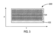
図3は、いくつかの実施例に従って、波状インターコネクト104を含むインターコネクトアセンブリ300の上面の断面図を模式的に示している。そして、図4は、いくつかの実施例に従って、波状インターコネクト104を含むインターコネクトアセンブリ300の側面の断面図を模式的に示している。見て分かるように、波状インターコネクト104は、フレキシブル基板102上に配置されてよく、かつ、フレキシブルパッシベーション層108は、波状インターコネクト104の上に配置されてよい。フレキシブル基板102、波状インターコネクト104、および、フレキシブルパッシベーション層108は、図1と図2に関連して説明された実施例と共に動いてよく、そして、その逆もまた同様である。
FIG. 3 schematically illustrates a top cross-sectional view of an
いくつかの実施例において、フレキシブル基板102は、図3を見て分かるように、x方向とy方向において一般的に拡がり得る平面を定めてよい。いくつかの実施例において、波状インターコネクト104は、x方向、上記平面と同一平面であってよい、においてICデバイス(例えば、図1−図2のICデバイス106a、106b)の電気信号をルーティングするように構成されてよい。波状インターコネクトは、お互いについて平行に走ってよく、そして、図を見て分かるように、x方向とy方向に垂直な方向(例えば、図4のz方向)から見たときに、直線を有してよい。いくつかの実施例において、波状インターコネクト104は、図4を見て分かるように、x方向に対して垂直であり、かつ、フレキシブル基板102によって定められる平面と同一平面である方向(例えば、図3のy方向)から見たときに、波状プロフィールを有してよい。
In some embodiments, the
図3と図4に関連して説明されたような波状インターコネクト104の波状プロフィールのコンフィグレーションにより、z方向から見たときに(例えば、図3のように上面から見たときに)波状プロフィールを有する蛇行したインターコネクトを有しているICアセンブリと比較して、ICアセンブリ(例えば、図1のICアセンブリ100)において、より高いインターコネクト密度ができる。例えば、そうした蛇行インターコネクトのうち一つの蛇行インターコネクトは、約100ミクロンの幅のラインと約1.5ミリの蛇行幅を有してよく、ミリメートルあたり約1I/O接続のインターコネクト密度を提供する。他方では、一つの実施例において、本開示に係る波状インターコネクト104のうち個々の波状インターコネクトは、約10ミクロンのライン幅(例えば、y方向におけるもの)を有してよく、そして、隣接する波状インターコネクト間のスペースは、約10ミクロン(隣接する波状インターコネクト間のピッチが約20ミクロン)であり、ミリメートルあたり約50I/O接続のインターコネクト密度を提供する。従って、本開示に係る波状インターコネクト104は、同様な曲げ及び/又は伸ばし強度について、蛇行インターコネクトと比較して、約50倍またはそれ以上の倍率でインターコネクト密度を増加させ得るものである。波状インターコネクト104は、例えば、ミリメートルあたり約10から100I/O接続を含んでいる他の実施例において、他の適切なインターコネクト密度を有してよい。いくつかの実施例において、波状インターコネクト104のそれぞれは、厚さ(例えば、z方向におけるもの)を有してよい。いくつかの実施例において、厚さに対する半アンプ(semi−amplitude)の割合は、10より大きいか、または、同じであってよい。
The configuration of the corrugated profile of the
波状インターコネクト104の波状プロフィールは、半アンプ(例えば、ピークトゥピークのアンプの半分)を有してよい。いくつかの実施例においては、波状インターコネクト104のライン幅に対する半アンプの割合が、1:2、または、1/2より大きくてよい。より柔らかく/よりフレキシブルな材料(例えば、PDMS)を有しているフレキシブル基板102について、波状インターコネクト104のライン幅に対する半アンプの割合は、フレキシブル基板102を効果的に延ばし、及び/又は、曲げることができるように、1:15、または、1/15より大きくてよい。破壊することのない伸ばし、及び/又は、曲げといった屈曲に耐えるための波状インターコネクト104の有効性は、ライン幅に対する半アンプの割合に基づいている。一方で、いくつかの実施例に従って、インターコネクトの厚さとライン幅は、ほとんど無関係である。しかしながら、上記の蛇行インターコネクトについて、そうした屈曲に耐えるための有効性は、蛇行インターコネクトのライン幅に対する蛇行幅の割合に基づくものであってよい。波状インターコネクト104により、フィルム厚さをコントロールするためのプロセスは、ライン幅をコントロールするためのプロセスよりも正確であり得るという少なくとも一つの理由のために、ずっと高いインターコネクト密度ができる。例えば、波状インターコネクト104のうち一つの波状インターコネクトは、10ミクロンのライン幅/スペース、1ミクロンの厚さ、および、50ミクロンの半アンプを有してよい。一方、蛇行インターコネクトは、20ミクロンのライン幅/スペース、および、1ミリメートルの蛇行幅を有してよく、同様な伸ばし、及び/又は、曲げの回復力を提供する。そうした事例において、波状インターコネクトは、蛇行インターコネクトよりも約50倍以上、または、それより大きいインターコネクト密度を提供する。
The wavy profile of the
いくつかの実施例において、フレキシブル基板102と波状インターコネクト104は、x方向において伸び、及び/又は、z方向において曲がるように構成されてよい。フレキシブル基板102と波状インターコネクト104は、他の実施例において他の適切な方向において、伸び、及び/又は、曲がるように構成されてよい。
In some embodiments, the
図4の描かれた実施例において、波状インターコネクト104の波状プロフィールは、曲がったプロフィールである(例えば、丸められた端を有している)。他の実施例において、波状プロフィールは、例えば、三角形状、長方形状、または、不規則な形状を含む他の形状を有してよい。曲がった波状プロフィールは、鋭い角を有している波状プロフィールより望ましいものであり得る。応力集中は、鋭い角と同時に発生し、フレキシブル基板102を変形し得るものだからである。
In the depicted embodiment of FIG. 4, the wave profile of the
図5aから図5fは、いくつかの実施例に従って、製造の様々なステージの最中におけるICアセンブリ500の一つの実施例に係る側面の断面図を模式的に示している。いくつかの実施例において、図5aから図5fに関連して説明される技術は、WIBを形成するために使用されてよい。様々な実施例に従って、ICアセンブリ500は、図1−図2のICアセンブリ100に関連して説明される実施例を用いて動作してよい。その逆もまた同様である。
FIGS. 5a through 5f schematically illustrate side cross-sectional views of one embodiment of an
図5aを参照すると、ICアセンブリ500が、フレキシブル基板102の表面に波状プロフィールを形成した後に続いて、描かれている。波状プロフィールは、フレキシブル基板102の波状プロフィールの上に形成されることになる波状インターコネクトの波状プロフィールに対応してよい。波状プロフィールは、例えば、印刷、モールディング、または、リソグラフィプロセスを含む、種々の適切な技術に従って形成されてよい。波状プロフィールは、他の実施例において、他の適切な技術を使用して形成されてよい。
Referring to FIG. 5 a,
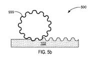
図5bを参照すると、ICアセンブリ500が、グラビア印刷プロセスを使用してフレキシブル基板102の表面に波状プロフィールを形成している最中に、描かれている。グラビア印刷プロセスにおいて、フレキシブル基板102は、フレキシブル基板102よりも固い材料で構成された印刷エレメント555を使用する波状プロフィールパターンを用いてインプリント(imprint)されてよい。印刷エレメント555は、フレキシブル基板102の表面上を転がってよく、そして、波状プロフィールを作成するように、フレキシブル基板102の表面に、印刷エレメント555の表面上のパターンに対応するギザギザ(indentation)を形成してよい。いくつかの実施例において、印刷プロセスは、印刷のためのより柔らかな材料を提供するように、フレキシブル基板102のキュアリング(curing)より先に実行される。
Referring to FIG. 5b, the
図5cを参照すると、ICアセンブリ500が、けば状の(fuzzy)リソグラフィプロセスを使用してフレキシブル基板102の表面に波状プロフィールを形成している最中に、描かれている。けば状のリソグラフィプロセスは、例えば、フレキシブル基板102の上に感光性(photodefinable)材料557をデポジット(deposit)すること、および、パターン化することを含んでよい。感光性材料557は、フレキシブル基板102に波状プロフィールを形成するように、グレースケールリソグラフィ、部分的にフォトトランスペアレントな(phototransparent)レジスト、低解像度の感光性材料、深度焦点外れ(out of depth focus)、または、他の適切な技術を使用して、プロセスされてよい。
Referring to FIG. 5c, the
図5dを参照すると、ICアセンブリ500が、一つまたはそれ以上の波状インターコネクト104を形成するために波状プロフィールの上に金属をデポジットした後に続いて、描かれている。金属は、例えば、付加的(additive)または減算的(substractive)プロセスを含む、あらゆる適切なプロセスを使用してデポジットされてよい。いくつかの実施例において、金属は、単一のフィルムとして最初にデポジットされ、そして、その後に続いて、波状インターコネクト104の個別のラインを形成するようにパターン化されてよい。
Referring to FIG. 5 d,
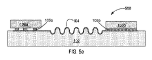
図5eを参照すると、ICアセンブリ500が、フレキシブル基板102上に一つまたはそれ以上のICデバイス106a、106bをマウントした後に続いて、描かれている。ICデバイス106a、106bは、SMTまたは他の適切なマウント技術を使用して、フレキシブル基板102と直接的に接続されてよい。いくつかの実施例において、ICデバイス106aは、例えば、バンプまたはピラーといった、ダイインターコネクト構造体105aを使用して波状インターコネクト104と接続されてよい。いくつかの実施例において、ICデバイス106bは、ACFを使用して波状インターコネクト104と接続されてよい。ICデバイス106a、106bは、他の実施例において、他の適切な技術を使用してフレキシブル基板102と接続されてよい。
Referring to FIG. 5e, an
図5fを参照すると、ICアセンブリ500が、フレキシブル基板104上にフレキシブルパッシベーション層108を形成した後に続いて、描かれている。いくつかの実施例において、フレキシブルパッシベーション層108は、波状インターコネクト104をカバーするように、フレキシブル基板102上に電気的な絶縁材料をデポジットすることによって形成されてよい。いくつかの実施例において、フレキシブルパッシベーション層108の材料は、ICデバイス106a、106bを部分的に、または、完全にカプセル化するようにデポジットされてよい。フレキシブルパッシベーション層108の材料は、例えば、モールディング及び/又はラミネーションプロセスを含む、あらゆる適切なプロセスを使用してデポジットされてよい。ICアセンブリ500は、曲げられ、伸ばされ、または、そうでなければ別の形状(例えば、図2の曲がったコンフィグレーション)へと曲げられてよい。
Referring to FIG. 5 f,
図6aから図6cは、いくつかの実施例に従って、製造の様々なステージの最中におけるICアセンブリ600の一つの実施例に係る側面の断面図を模式的に示している。いくつかの実施例において、図6aから図6cに関連して説明される技術は、WIBを形成するために使用されてよい。様々な実施例に従って、ICアセンブリ600は、図1−図2のICアセンブリ100に関連して説明される実施例を用いて動作してよい。その逆もまた同様である。
Figures 6a to 6c schematically illustrate side cross-sectional views of one embodiment of an
図6aを参照すると、ICアセンブリ600が、フレキシブル基板102上に波状インターコネクトのルーティングライン504を形成した後に続いて、描かれている。いくつかの実施例において、フレキシブル基板102は、キャリア570と一時的に結合されてよく、そして、見て分かるように、キャリア570と離れて向いている実質的に平坦な表面を有している。フレキシブル基板102は、金属のデポジションに先立ってキャリア570と結合されてよい。いくつかの実施例において、金属は、フィルムとしてデポジットされたブランケット(blanket)であってよく、波状インターコネクトのルーティングライン504を形成するように、例えば、エッチ(etch)及び/又はリソグラフィプロセスを使用して実質的にパターン化された、金属層を提供する。他の実施例において、金属は、波状インターコネクトのルーティングライン504を形成するように、選択的にデポジットされてよい(例えば、インク印刷プロセス)。
Referring to FIG. 6 a,
図6bを参照すると、ICアセンブリ600が、フレキシブル基板102からキャリア570を分離し、そして、波状プロフィールを有する波状インターコネクト104を作成するように金属とフレキシブル基板102を成形(shaping)した後に続いて、描かれている。いくつかの実施例において、フレキシブル基板102は、キャリア570から離されてよく、そして、その後に続いて、金属とフレキシブル基板102を局所的に変形するように、例えば、プレスまたはケミカル(chemical)プロセスを使用して、フレキシブル基板102が成形されてよい。いくつかの実施例においては、見て分かるように、形成プロセスは、波状プロフィールが、インターコネクトフレキシブル基板102の反対側に形成されるようにしてよい。
Referring to FIG. 6b, following the
図6cを参照すると、ICアセンブリ600が、フレキシブル基板102上にICデバイス106a、106bをマウントし、そして、フレキシブル基板102上にフレキシブルパッシベーション層108を成形した後に続いて、描かれている。ICデバイス106a、106bは、図5eに関連して説明された技術に従って、マウントされてよい。いくつかの実施例において、フレキシブルパッシベーション層108は、見て分かるように、波状インターコネクト104の波状プロフィールを閉じ込める(lock in)ようにフレキシブル基板102の反対側において形成されてよい。
Referring to FIG. 6 c, an
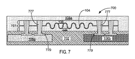
図7は、いくつかの実施例に従って、ICアセンブリ700の別の実施例に係る側面の断面図を模式的に示している。様々な実施例に従って、ICアセンブリ700は、波状インターコネクトモジュール(WIM)コンフィグレーションにおいて構成されてよい。
FIG. 7 schematically illustrates a cross-sectional side view of another embodiment of an
いくつかの実施例において、波状インターコネクト104は、フレキシブル基板102とパッシベーション層108を含んでいるモジュール781の中にエンベッドされている。いくつかの実施例において、モジュール781は、フレキシブル基板と波状インターコネクト104だけを含んでよい。例えば、フレキシブルパッシベーション層108aが、いくつかの実施例において、波状インターコネクト104の上にデポジットされてよい。
In some embodiments, the
波状インターコネクト104は、別のフレキシブル基板702の中にエンベッドされたICデバイス106a、106bと電気的に接続されてよい。見て分かるように、例えば、めっきスル―ホール(PTH)またはビア(via)といった、一つまたはそれ以上のサブストレート貫通インターコネクト777を使用するものである。いくつかの実施例において、サブストレート貫通インターコネクト777は、見て分かるように、フレキシブル基板102と702の少なくとも一部分を通じて延びてよい。
The
波状インターコネクト104それぞれは、ICデバイス106a、106bにおいて形成されたパッド779に対応するパッドに電気的に接続されてよい。いくつかの実施例において、別のフレキシブルパッシベーション層108aが、見て分かるように、波状インターコネクト104を含んでいるモジュール781をカプセル化するように形成されてよい。フレキシブル基板702及び/又はパッシベーション層108aは、フレキシブル基板102及び/又はパッシベーション層108に関連してそれぞれに説明された実施例を用いて動作してよい。
Each
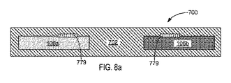
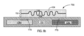
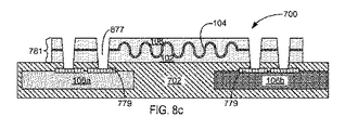
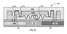
図8aから図8fは、いくつかの実施例に従って、製造の様々なステージの最中における図7のICアセンブリ700の実施例に係る側面の断面図を模式的に示している。様々な実施例に従って、ICアセンブリ700は、図7に関連してそれぞれに説明された実施例を用いて動作してよく、そして、その逆もまた同様である。
FIGS. 8a to 8f schematically show side cross-sectional views of the embodiment of the
図8aを参照すると、ICアセンブリ700が、フレキシブル基板702の中にICデバイス106a、106bをエンベッドした後に続いて、描かれている。ICデバイス106a、106bは、例えば、積み上げ(build−up)ラミネーションプロセスを含む、多種多様な適切な技術を使用してエンベッドされてよい。パッド779は、いくつかの実施例において、エンベッドされる以前に、ICデバイス106a、106bにおいて形成されてよい。
Referring to FIG. 8a, an
図8bを参照すると、ICアセンブリ700が、フレキシブル基板702を伴う波状インターコネクト104を含んでいるモジュール781を結合した後に続いて、描かれている。モジュール781は、図5a−図5dに関連して説明された動作を実行することによって形成されてよい。いくつかの実施例において、パッシベーション層(例えば、図5fのフレキシブルパッシベーション層108)は、モジュール781を形成するように、図5dのICアセンブリ500の上にデポジットされてよい。
Referring to FIG. 8 b,
モジュール781は、例えば、ラミネーションを含む適切な技術を使用して、または、接着剤を使用して、フレキシブル基板702と結合されてよい。いくつかの実施例において、モジュール781は、あらゆる適切なアライメント(alignment)技術を使用して、モジュール781をフレキシブル基板702と結合する以前に、フレキシブル基板702と整列されてよい。
図8cを参照すると、ICアセンブリ700が、モジュール781を通じて形成されるサブストレート貫通インターコネクトに対応する開口877を形成した後に続いて、描かれている。いくつかの実施例において、一つまたはそれ以上のパッド779は、サブストレート貫通インターコネクトのアライメントと形成を促進するように、モジュール781とフレキシブル基板702との間におけるアライメントの不確実性よりも大きなサイズであってよい。開口877は、例えば、パターン化とエッチング、または、レーザードリル(laser drilling)といった穴あけを含むアライメント適切な技術を使用して形成されてよい。いくつかの実施例において、隣接するパッド779は、約300ミクロン、または、それより小さいピッチで置かれてよい。
Referring to FIG. 8c,
図8dを参照すると、ICアセンブリ700が、見て分かるように、波状インターコネクト104をICデバイス106a、106bと電気的に接続するサブストレート貫通インターコネクト777を形成するように開口877の中に金属をデポジットし、そして、モジュール781の上にフレキシブルパッシベーション層108aをデポジットした後に続いて、描かれている。いくつかの実施例において、金属は、サブストレート貫通インターコネクト777を形成するために、開口877を実質的に埋めるようにデポジットされてよい。他の実施例において、金属は、開口877を部分的に埋めるようにデポジットされてよい。サブストレート貫通インターコネクト777は、他の実施例において、図8e−図8fに関連して説明された他の技術を使用して形成されてよい。
Referring to FIG. 8d,
図8eを参照すると、ICアセンブリ700が、より高い密度の電気ルーティングを提供するために別の技術を使用して開口877a、877bを形成した後に続いて、描かれている。例えば、図8において、開口877a、877bの形成は、モジュール781の中、及び/又は、フレキシブル基板702の中にエンベッドされたICデバイス106a、106bの表面上のいずれかにおいて事前にマップされたパッド(pre−mapped pad)を使用して促進されてよい。マスキング層108bは、モジュール781とフレキシブル基板702の上に形成されてよい。いくつかの実施例において、一つまたはそれ以上の開口877aが、マスキング層108bとモジュール781のフレキシブルパッシベーション層108を通して形成されてよく、波状インターコネクト104の波状インターコネクトを露出する。ICデバイス106a、106bにおける一つまたはそれ以上の対応するパッド779を露出するために、一つまたはそれ以上の開口877bが、マスキング層108bを通して形成されたよい。いくつかの実施例において、マスキング層108bは、フレキシブルな材料で構成されてよい。例えば、マスキング層108bは、いくつかの実施例において、フレキシブル基板102及び/又はフレキシブルパッシベーション層108に関連して説明された実施例を用いて動作してよい。
Referring to FIG. 8e,
図8fを参照すると、ICアセンブリ700が、見て分かるように、波状インターコネクト104をICデバイス106a、106bと電気的に接続するサブストレート貫通インターコネクト777a、777bを形成するように図8eの開口877a、877bの中に金属をデポジットし、そして、マスキング層108bの上にフレキシブルパッシベーション層108aをデポジットした後に続いて、描かれている。いくつかの実施例において、金属は、サブストレート貫通インターコネクト777a、777bを形成するために、図8eの開口877a、877bを実質的に埋めるようにデポジットされてよい。他の実施例において、金属は、開口877を部分的にだけ埋めるようにデポジットされてよい。例えば、金属は、見て分かるように、開口877a、877bを並べ、そして、サブストレート貫通インターコネクト777aとサブストレート貫通インターコネクト777bとの間のルーティングを提供してよい。他の実施例において、金属は、開口877を埋めるようにデポジットされてよい。ICデバイス106a、106b上のサブストレート貫通インターコネクト777(例えば、開口877bに対応するもの)からモジュール781上のサブストレート貫通インターコネクト777(例えば、開口877aに対応するもの)へのルーティングをパターン化するために、ダイレクトレーザ画像化(DLI)が使用されてよい。いくつかの実施例において、見て分かるように、フレキシブルパッシベーション層108aの材料は、開口877a、877bを部分的に埋めてよい。
Referring to FIG. 8f, the
図9は、いくつかの実施例に従って、ICアセンブリ(例えば、図1−図2のICアセンブリ100または図7のICアセンブリ700)を製造する方法のためのフローチャートを模式的に示している。方法900に係るアクション(action)は、図1−図8に関連して説明された技術を用いて動作してよい。
FIG. 9 schematically illustrates a flowchart for a method of manufacturing an IC assembly (eg,
902において、方法900は、フレキシブル基板(例えば、図5cのフレキシブル基板102)を提供するステップを含んでよい。様々な実施例に従って、フレキシブル基板は、一つの平面を定めてよい。
At 902, the
904において、方法900は、フレキシブル基板上に波状インターコネクト(例えば、図5dまたは図6bの波状インターコネクト104)を形成するステップを含んでよい。様々な実施例に従って、波状インターコネクトは、フレキシブル基板によって定められる平面と同一平面である第1方向においてICデバイスの電気信号をルーティングするように構成されてよい。波状インターコネクトは、第1方向と垂直で、かつ、平面と同一平面にある第2方向からみるとき、波状プロフィールを有してよい。
At 904, the
いくつかの実施例において、波状インターコネクトを形成するステップは、フレキシブル基板の表面に波状プロフィールを形成すること(例えば、図5a−図5cに関連して説明及び/又は描かれたように)、そして、その後に続いて、波状プロフィールの上に金属をデポジットすること(例えば、図5dに関連して説明及び/又は描かれたように)を含んでよい。いくつかの実施例においては、波状プロフィールを形成するために、印刷、モールディング、またはリソグラフィプロセスが使用されてよい。他の実施例において、波状インターコネクトを形成するステップは、フレキシブル基板の実質的に平坦な表面上に金属をデポジットすること(例えば、図6aに関連して説明及び/又は描かれたように)、そして、その後に続いて、波状プロフィールを作成するために金属とフレキシブル基板を成形すること(例えば、図6bに関連して説明及び/又は描かれたように)を含んでよい。 In some embodiments, forming the corrugated interconnect includes forming a corrugated profile on the surface of the flexible substrate (eg, as described and / or depicted in connection with FIGS. 5a-5c), and , Followed by depositing metal on the wavy profile (eg, as described and / or depicted in connection with FIG. 5d). In some embodiments, a printing, molding, or lithographic process may be used to form a wavy profile. In other embodiments, forming the corrugated interconnect includes depositing metal on a substantially planar surface of the flexible substrate (eg, as described and / or depicted in connection with FIG. 6a), And subsequently, may include shaping the metal and flexible substrate to create a wavy profile (eg, as described and / or depicted in connection with FIG. 6b).
906において、方法900は、一つまたはそれ以上のICデバイス(例えば、図1−図2および図7のICデバイス106a、106b)を波状インターコネクトと電気的に接続するステップを含んでよい。いくつかの実施例において、一つまたはそれ以上のICデバイスは、例えば、半田ジョイントを形成するといったSMT、等(例えば、図5eまたは図6cに関連して説明及び/又は描かれたように)を使用して、一つまたはそれ以上のICデバイスを波状インターコネクトと接続することによって、一つまたはそれ以上のICデバイスがフレキシブル基板上にマウントされてよい。他の実施例において、一つまたはそれ以上のICデバイスは、別のフレキシブル基板(例えば、図8のフレキシブル基板702)の中にエンベッドされてよく、波状インターコネクトのフレキシブル基板と接続されてよい。波状インターコネクトとエンベッドされた一つまたはそれ以上のICデバイスとの間に電気的接続が形成されてよい。いくつかの実施例において、電気的接続は、サブストレート貫通インターコネクト(図8dのサブストレート貫通インターコネクト777または図8fのサブストレート貫通インターコネクト777a、777b)であってよい。2つまたはそれ以上のICデバイスが波状インターコネクトと接続される事例では、波状インターコネクトが、2つまたはそれ以上のICデバイス間において電気信号をルーティングするように構成されてよい。
At 906, the
908において、方法900は、フレキシブル基板上にパッシベーション層を形成するステップを含んでよい。パッシベーション層(例えば、図5fのパッシベーション層108)は、いくつかの実施例において、波状インターコネクトをカバーするようにデポジットされてよい。いくつかの実施例においては、パッシベーション層が、フレキシブル基板上に一つまたはそれ以上のICデバイスをマウントすることの後に続いてデポジットされてよい。フレキシブル基板上にデポジットされたときに、一つまたはそれ以上のICデバイスの上にパッシベーション層がデポジットされるようにである(例えば、図5fに関連して説明及び/又は描かれたように)。いくつかの実施例において、パッシベーション層は、波状プロフィールを閉じ込めるようにフレキシブル基板の反対側においてデポジットされてよい(例えば、図6cに関連して説明及び/又は描かれたように)。いくつかの実施例において、パッシベーション層は、モジュール(例えば、図8bのモジュール781)を形成するように波状インターコネクトの上にデポジットされてよい。いくつかの実施例においては、モジュールをカプセル化するようにパッシベーション層(例えば、図8dまたは図8fのパッシベーション層108a)がデポジットされてよい。
At 908, the
様々なオペレーションが、請求される技術的事項を理解することにおいて最も役に立つやり方において、複数の個別のオペレーションとして順番に説明されている。しかしながら、説明の順番は、これらのオペレーションが必然的に順番に依存するものであることを意味するものとして理解されるべきではない。 The various operations are described in turn as a plurality of individual operations in a manner that is most useful in understanding the claimed technical matter. However, the order of description should not be understood to mean that these operations are necessarily order dependent.
本開示の実施例は、あらゆる適切なハードウェア及び/又はソフトウェアを使用して、望むように構成するためにシステムの中へ実装されてよい。図10は、いくつかの実施例に従って、ここにおいて説明されるような波状インターコネクト(例えば、図1−図2または図7の波状インターコネクト)を有するICアセンブリ(例えば、図1−図2のICアセンブリ100または図7のICアセンブリ700)を含むコンピューティングデバイスに係る一つの実施例を模式的に示している。コンピューティングデバイス1000は、マザーボード1002といったボードを収納してよい(例えば、ハウジング1008の中に)。マザーボード及び/又はハウジングは、いくつかの実施例において、フレキシブルな材料を含んでよく、コンピューティングデバイスの伸ばし及び/又は曲げができる。マザーボード1002は、数多くのコンポーネントを含んでよい。これらに限定されるわけではないが、プロセッサ1004と少なくとも一つの通信チップ1006を含んでいる。プロセッサ1004は、物理的かつ電気的にマザーボード1002に接続されている。いくつかの実施例において、少なくとも一つの通信チップ1006は、また、物理的かつ電気的にマザーボード1002に接続されている。さらなる実施例において、通信チップ1006は、プロセッサ1004の一部分であってよい。
Embodiments of the present disclosure may be implemented into the system to configure as desired using any suitable hardware and / or software. 10 illustrates an IC assembly (eg, the IC assembly of FIGS. 1-2) having a corrugated interconnect as described herein (eg, the corrugated interconnect of FIG. 1-2 or FIG. 7), according to some embodiments. 10 schematically illustrates one embodiment of a computing device including 100 or the
アプリケーションに応じて、コンピューティングデバイス1000は、物理的かつ電気的にマザーボード1002に接続されても、されなくてもよい他のコンポーネントを含んでよい。これらの他のコンポーネントは、これらに限定されるわけではないが、揮発性メモリ(例えば、DRAM)、不揮発性メモリ(例えば、ROM)、フラッシュメモリ、グラフィクスプロセッサ、デジタルシグナルプロセッサ、暗号プロセッサ、チップセット、オーディオコーデック、ビデオコーデック、パワーアンプ、全地球測位システム(GPS)デバイス、コンピューティングデバイスパスワード、ガイガーカウンタ、加速度計、ジャイロスコープ、スピーカ、カメラ、および、大容量ストレージデバイス(ハードディスクドライブ、コンパクトディスク(CD)、デジタル多目的ディスク(DVD)、等)を含んでよい。
Depending on the application, the
通信チップ1006は、コンピューティングデバイス100へ、又は、からのデータ転送のための無線通信をできるようにし得る。用語「無線(”wireless”)」及びその派生語は、非固体の媒体を通じた変調された電磁気的放射の使用を通してデータを通信し得る、回路、デバイス、システム、方法、技術、通信チャンネル、等を表わすために使用されてよい。その用語は、関連するデバイスが、いくつかの実施例においてはそうでないが、電線を全く有さないことを意味するものではない。通信チップ1006は、数多くの無線規格またはプロトコルのうちあらゆるものを実施してよく、これらに限定されるわけではないが、米国電気電子学会(IEEE)標準規格を含んでいる。Wi−Fi(IEEE802.11ファミリー)、IEEE802.16標準規格(例えば、IEEE802.16−2005年改正)、あらゆる改正、変更、及び/又は、リビジョンと併せたロングタームエボリューション(LTE)プロジェクト(例えば、アドバンストLTEプロジェクト、ウルトラモバイルブロードバンド(UMB)プロジェクト(”3GPP2”としても参照されるもの))を含んでいる。IEEE802.16コンパチブルブロードバンドワイヤレスアクセス(BWA)ネットワークは、一般的にWiMAXとして参照される、Worldwide Interoperability for Microwave Accessを表わす頭字語であり、IEEE802.16標準規格について適合性と相互運用性の試験を合格した製品のための証明マークである。通信チップ1006は、Global System for Mobile Communication(GSM)(登録商標)、General Packet Radio Service(GPRS)、Universal Mobile Telecommunications System(UTMS)、High Speed Packet Access(HSPA)、Evolved HSPA(E−HSPA)、または、LTEネットワーク、に従って動作してよい。通信チップ1006は、Enhanced Data for GSM Evolution(EDGE)、GSM EDGE Radio Access Network(GERAN)、Universal Terrestrial Radio Access Network(UTRAN)、または、Evolved UTRAN(E−UTRAN)、に従って動作してよい。通信チップ1006は、Code Division Mutiple Access(CDMA)、Time Division Multiple Access(TDMA)、Digital Enhanced Cordless Telecommunications(DECT)、Evolution−Data Optimized(EV−DO)、それらの派生物、に従って動作してよい。3G、4G、5G、および、それを超えるものとして表されるあらゆる他の無線プロトコルも同様である。通信チップ1006は、他の実施例において、他の無線プロトコルに従って、動作してよい。
コンピューティングデバイス1000は、複数の通信チップ1006を含んでよい。例えば、第1通信チップ1106は、Wi−Fiおよびブルートゥース(登録商標)といった近距離無線通信専用であってよく、そして、第2通信チップ1106は、GPS、EDGE、GPRS、CDMA、WiMAX、LTE、EV−DO、その他、といった長距離無線通信専用であってよい。
The
コンピューティングデバイス1000のプロセッサ1004は、ここにおいて説明されるように、波状インターコネクト(例えば、図1−図2、または図7の波状インターコネクト104)を有するICアセンブリ(例えば、図1−図2のICアセンブリ100、または図7のICアセンブリ700)の中にパッケージされてよい。例えば、ここにおいて説明されるように、マザーボード1002は、フレキシブル基板(例えば、図1−図2のフレキシブル基板102、または図7のフレキシブル基板702)に接続されるか、その一部分であってよく、そして、プロセッサ1004または他のICデバイス(例えば、通信チップ1006、メモリデバイス、コンパス、等)は、一つまたはそれ以上のICデバイス(例えば、ICデバイス106a、106b)であってよい。他の適切なコンフィグレーションが、ここにおいて説明される実施例に従って、実施されてよい。用語「プロセッサ(”processor”)」は、レジスタ及び/又はメモリからの電子データを処理する、あらゆるデバイスまたはデバイスの一部を参照してよく、電子データをレジスタ及び/又はメモリに保管され得る他の電子データへと変換するものである。
The
様々な実施において、コンピューティングデバイス1000は、ラップトップ、ネットブック、ノートブック、ウルトラブック、スマートフォン、タブレット、パーソナルデジタルアシスタント(PDA)、ウルトラモバイルPC、モバイルフォン、デスクトップコンピュータ、サーバ、プリンタ、スキャナ、モニタ、セットトップボックス、エンターテイメントコントロール装置、デジタルカメラ、ポータブル音楽プレーヤ、または、デジタルビデオレコーダ、であってよい。コンピューティングデバイス1000は、いくつかの実施例において、フレキシブルなモバイルコンピューティングデバイスであってよい。いくつかの実施例において、コンピューティングデバイスのフレキシブルなICアセンブリは、人が身に付けることができる(wearable)なもの(例えば、衣服またはアクセサリー製品の中に組み込まれたもの)であってよい。将来の実施において、コンピューティングデバイス1000は、データを処理するあらゆる他の電子デバイスであってよい。
In various implementations, the
様々な実施例において、本開示は、装置(例えば、インターコネクトアセンブリ)を説明している。インターコネクトアセンブリの第1実施例は、一つの平面を定めるフレキシブル基板と、フレキシブル基板上に配置され、かつ、集積回路(IC)デバイスの電気信号を平面と同一平面にある第1方向においてルーティングするように構成されている波状インターコネクトであり、波状インターコネクトは、第1方向に垂直であり、かつ、平面と同一平面にある第2方向から見て波状プロフィールを有している、波状インターコネクトと、を含む。第2実施例は、第1実施例に係るインターコネクトアセンブリを含んでよく、波状インターコネクトは、第1方向と第2方向に対して垂直な第3方向から見て直線プロフィールを有している。第3実施例は、第1実施例に係るインターコネクトアセンブリを含んでよく、フレキシブル基板と波状インターコネクトは、第1方向において伸び、及び/又は、第1方向と第2方向に対して垂直な第3方向において曲がるように構成されている。第4実施例は、第1実施例に係るインターコネクトアセンブリを含んでよく、波状インターコネクトは、第2方向から見て幅を有し、波状プロフィールは、半アンプを有しており、かつ、半アンプに対する幅の割合(幅/半アンプ)は、1/2より大きいか等しい。第5実施例は、第4実施例に係るインターコネクトアセンブリを含んでよく、波状インターコネクトは、第1方向と第2方向に対して垂直な第3方向から見て厚さを有し、かつ、厚さに対する半アンプの割合(半アンプ/厚さ)は、10より大きいか等しい。第6実施例は、第1乃至第5いずれかの実施例に係るインターコネクトアセンブリを含んでよく、波状プロフィールは、曲がったプロフィールである。第7実施例は、第1乃至第5いずれかの実施例に係るインターコネクトアセンブリを含んでよく、波状インターコネクトは、第1方向において波状インターコネクトと平行に走る複数の波状インターコネクトのうちの一つである。第8実施例は、第1乃至第5いずれかの実施例に係るインターコネクトアセンブリを含んでよく、波状インターコネクトは金属を含み、かつ、フレキシブル基板は、ポリマーを含む。 In various embodiments, the present disclosure describes an apparatus (eg, an interconnect assembly). A first embodiment of an interconnect assembly is configured to route a flexible substrate that defines a plane and an electrical signal of an integrated circuit (IC) device that is disposed on the flexible substrate in a first direction that is coplanar with the plane. A corrugated interconnect, wherein the corrugated interconnect is perpendicular to the first direction and has a corrugated profile when viewed from a second direction that is coplanar with the plane. . The second embodiment may include an interconnect assembly according to the first embodiment, and the corrugated interconnect has a linear profile when viewed from a third direction perpendicular to the first direction and the second direction. The third embodiment may include an interconnect assembly according to the first embodiment, wherein the flexible substrate and the corrugated interconnect extend in the first direction and / or are perpendicular to the first direction and the second direction. It is configured to bend in the direction. The fourth embodiment may include an interconnect assembly according to the first embodiment, wherein the corrugated interconnect has a width when viewed from the second direction, the corrugated profile includes a half amplifier, and the half amplifier. The ratio of width to (width / half amplifier) is greater than or equal to 1/2. The fifth embodiment may include an interconnect assembly according to the fourth embodiment, wherein the corrugated interconnect has a thickness when viewed from a third direction perpendicular to the first direction and the second direction, and the thickness is The ratio of half amplifier to thickness (half amplifier / thickness) is greater than or equal to 10. The sixth embodiment may include an interconnect assembly according to any of the first to fifth embodiments, and the wavy profile is a curved profile. The seventh embodiment may include an interconnect assembly according to any of the first to fifth embodiments, and the corrugated interconnect is one of a plurality of corrugated interconnects that run parallel to the corrugated interconnect in the first direction. . The eighth embodiment may include an interconnect assembly according to any of the first to fifth embodiments, where the corrugated interconnect includes a metal and the flexible substrate includes a polymer.
様々な実施例において、本開示は、ICアセンブリの製造方法を説明している。方法に係る第9の実施例は、フレキシブル基板を備えるステップであり、フレキシブル基板は一つの平面を定めるステップと、フレキシブル基板上に波状インターコネクトを形成するステップであり、波状インターコネクトは、平面と同一平面にある第1方向において集積回路(IC)デバイスの電気信号をルーティングするように構成されており、波状インターコネクトは、第1方向に垂直であり、かつ、平面と同一平面にある第2方向から見て波状プロフィールを有している、ステップと、を含む。第10実施例は、第9実施例に係る方法を含んでよく、波状インターコネクトを形成するステップは、フレキシブル基板の表面において波状インターコネクトの表面上に波状プロフィールを形成するステップと、波状プロフィールの上に金属をデポジットするステップと、を含む。第11実施例は、第10実施例に係る方法を含んでよく、波状プロフィールを形成するステップは、印刷、モールディング、または、リソグラフィプロセスを使用するステップと、を含む。第12実施例は、第9実施例に係る方法を含んでよく、さらに、波状インターコネクトをカバーするように、フレキシブル基板上にパッシベーション層をデポジットするステップと、を含む。第13実施例は、第12実施例に係る方法を含んでよく、さらに、パッシベーション層をデポジットするステップの以前に、ICデバイスを波状インターコネクトと電気的に接続するステップと、を含み、パッシベーション層をデポジットするステップは、ICデバイスの上にパッシベーション層をデポジットするステップと、を含む。第14実施例は、第9実施例に係る方法を含んでよく、波状インターコネクトを形成するステップは、フレキシブル基板の実質的に平坦な表面上に金属をデポジットするステップと、波状プロフィールを作成するために、金属とフレキシブル基板を成形するステップと、を含む。第15実施例は、第14実施例に係る方法を含んでよく、金属は、フレキシブル基板の第2側面とは反対側に配置されたフレキシブル基板の第1側面上にデポジットされ、本方法は、さらに、フレキシブル基板上にICデバイスをマウントするステップと、波状プロフィールを閉じ込めるために、フレキシブル基板の第1側面および第2側面の上にフレキシブルパッシベーション層をデポジットするステップと、を含む。第16実施例は、第9実施例に係る方法を含んでよく、フレキシブル基板は、第1フレキシブル基板であり、本方法は、さらに、第2フレキシブル基板の中にICデバイスをエンベッドするステップと、第1フレキシブル基板を第2フレキシブル基板と接続するステップと、波状インターコネクトとICデバイスとの間に電気的な接続を形成するステップと、を含む。第17実施例は、第16実施例に係る方法を含んでよく、電気的な接続を形成するステップは、サブストレート貫通インターコネクトを形成するステップと、を含む。 In various embodiments, the present disclosure describes a method of manufacturing an IC assembly. A ninth embodiment of the method includes the steps of providing a flexible substrate, the flexible substrate defining a plane, and forming a corrugated interconnect on the flexible substrate, the corrugated interconnect being coplanar with the plane. The corrugated interconnect is configured to route an electrical signal of an integrated circuit (IC) device in a first direction, the corrugated interconnect being perpendicular to the first direction and viewed from a second direction that is coplanar with the plane. And having a wavy profile. The tenth embodiment may include the method according to the ninth embodiment, wherein forming the corrugated interconnect includes forming a corrugated profile on the surface of the corrugated interconnect at the surface of the flexible substrate; Depositing a metal. The eleventh embodiment may include a method according to the tenth embodiment, and forming the wavy profile includes using a printing, molding, or lithographic process. The twelfth embodiment may include the method according to the ninth embodiment, and further includes depositing a passivation layer on the flexible substrate to cover the corrugated interconnect. The thirteenth embodiment may include the method according to the twelfth embodiment, and further comprising the step of electrically connecting the IC device with the corrugated interconnect prior to the step of depositing the passivation layer. Depositing includes depositing a passivation layer over the IC device. The fourteenth embodiment may include the method according to the ninth embodiment, wherein forming the corrugated interconnect includes depositing metal on a substantially flat surface of the flexible substrate and creating a corrugated profile. Forming a metal and a flexible substrate. The fifteenth embodiment may include the method according to the fourteenth embodiment, wherein the metal is deposited on the first side of the flexible substrate disposed on the opposite side of the second side of the flexible substrate, the method comprising: Furthermore, mounting the IC device on the flexible substrate and depositing a flexible passivation layer on the first side and the second side of the flexible substrate to confine the wave profile. The sixteenth embodiment may include a method according to the ninth embodiment, wherein the flexible substrate is a first flexible substrate, and the method further includes the step of embedding an IC device in the second flexible substrate; Connecting the first flexible substrate to the second flexible substrate and forming an electrical connection between the corrugated interconnect and the IC device. The seventeenth embodiment may include the method according to the sixteenth embodiment, and the step of forming an electrical connection includes the step of forming a through-substrate interconnect.
様々な実施例において、本開示は、伸び縮み可能または折り曲げ可能な集積回路(IC)アセンブリを説明している。伸び縮み可能または折り曲げ可能なICアセンブリに係る第18の実施例は、集積回路(IC)デバイスと、一つの平面を定めるフレキシブル基板と、フレキシブル基板上に配置され、かつ、ICデバイスの電気信号を平面と同一平面にある第1方向においてルーティングするようにICデバイスと電気的に接続されている波状インターコネクトであり、波状インターコネクトは、第1方向に垂直であり、かつ、平面と同一平面にある第2方向から見て波状プロフィールを有している、波状インターコネクトと、を含む。第19実施例は、第18実施例に係るICアセンブリを含んでよく、波状インターコネクトは、第1方向と第2方向に対して垂直な第3方向から見て直線プロフィールを有している。第20実施例は、第18実施例に係るICアセンブリを含んでよく、ICデバイスは第1ICデバイスであり、ICアセンブリは、さらに、波状インターコネクトと電気的に接続された第2ICデバイスであり、波状インターコネクトは、第1ICデバイスと第2ICデバイスとの間で電気信号をルーティングするように構成されている、第2ICデバイスと、を含む。第21実施例は、第20実施例に係るICアセンブリを含んでよく、第1ICデバイスはダイであり、かつ、第2ICデバイスはセンサである。第22実施例は、第18実施例に係るICアセンブリを含んでよく、ICデバイスは、フレキシブル基板と直接的に接続されており、ICアセンブリは、さらに、波状インターコネクトとICデバイスの上に配置されたフレキシブルパッシベーション層を含む。第23実施例は、第22実施例に係るICアセンブリを含んでよく、波状インターコネクトは、フレキシブル基板の第1側面上に配置されており、フレキシブル基板の第2側面は、波状インターコネクトの波状プロフィールに対応する波状プロフィールを有しており、かつ、第2側面は、第1側面とは反対側に配置されている。第25実施例は、第18乃至第24いずれかの実施例に係るICアセンブリを含んでよく、ICアセンブリは、人が身に付けることができる。 In various embodiments, the present disclosure describes a stretchable or foldable integrated circuit (IC) assembly. An eighteenth embodiment of a stretchable or foldable IC assembly includes an integrated circuit (IC) device, a flexible substrate that defines a plane, and an electrical signal of the IC device disposed on the flexible substrate. A corrugated interconnect electrically connected to the IC device to route in a first direction coplanar with the plane, the corrugated interconnect being perpendicular to the first direction and coplanar with the plane And a wavy interconnect having a wavy profile when viewed from two directions. The nineteenth embodiment may include an IC assembly according to the eighteenth embodiment, and the corrugated interconnect has a linear profile when viewed from a third direction perpendicular to the first direction and the second direction. The twentieth embodiment may include an IC assembly according to the eighteenth embodiment, where the IC device is a first IC device, and the IC assembly is further a second IC device electrically connected to the corrugated interconnect, The interconnect includes a second IC device configured to route electrical signals between the first IC device and the second IC device. The twenty-first embodiment may include an IC assembly according to the twentieth embodiment, wherein the first IC device is a die and the second IC device is a sensor. The twenty-second embodiment may include an IC assembly according to the eighteenth embodiment, wherein the IC device is directly connected to the flexible substrate, and the IC assembly is further disposed on the corrugated interconnect and the IC device. A flexible passivation layer. The twenty-third embodiment may include an IC assembly according to the twenty-second embodiment, wherein the corrugated interconnect is disposed on the first side of the flexible substrate, and the second side of the flexible substrate is in the corrugated profile of the corrugated interconnect. It has a corresponding wavy profile and the second side is arranged on the opposite side of the first side. The twenty-fifth embodiment may include an IC assembly according to any of the eighteenth to twenty-fourth embodiments, and the IC assembly can be worn by a person.
種々の実施例は、上記の実施例のあらゆる適切な組み合わせを含んでよく、上記と結合的な形式において説明された実施例(例えば、「かつ(”and”)は「及び/又は(”and/or”)」であってよい)の代替的な実施例を含んでいる。さらに、いくつかの実施例は、インストラクションを有している一つまたはそれ以上の製造製品(例えば、固定のコンピュータで読取り可能な媒体)を含んでよく、実行されると、あらゆる上述された実施例に係る動作を結果として生じる。その上、いくつかの実施例は、上述された実施例の様々なオペレーションを実行するためのあらゆる適切な手段を有している装置またはシステムを含んでよい。 Various embodiments may include any suitable combination of the above-described embodiments, and the embodiments (eg, “and” and “and” described in conjunction with the above are “and”). / Or ")") is included. In addition, some embodiments may include one or more manufactured products (eg, fixed computer-readable media) having instructions and, when executed, any of the above-described implementations. An example operation results. Moreover, some embodiments may include an apparatus or system having any suitable means for performing the various operations of the embodiments described above.
上記に説明された実施例は、要約において記述されるものを含み、本開示に係る実施例を開示されたまさにその形式について徹底され、または、限定するように意図されたものではない。特定の実施と実施例が説明目的のためにここにおいて説明される一方で、当業者であれば認識するであろうように、本開示の範囲の中で種々の均等な変更が可能である。 The embodiments described above include those described in the summary and are not intended to be exhaustive or to limit the exact form in which the embodiments of the present disclosure are disclosed. While specific implementations and embodiments are described herein for purposes of illustration, various equivalent modifications are possible within the scope of the present disclosure, as those skilled in the art will recognize.
これらの変形は、上記の詳細な説明に照らして、本開示の実施例について行われ得るものである。以降の請求項において使用される用語は、本開示の種々の実施例を、明細書と請求項において開示される特定の実施例について限定するものと理解されるべきではない。むしろ、その範囲は、以降の請求項によって完全に決定されるべきものであり、請求項の解釈に係る確立された方針に従って理解されるべきである。
These variations can be made to the embodiments of the present disclosure in light of the above detailed description. The terms used in the following claims should not be construed to limit the various embodiments of the present disclosure to the specific embodiments disclosed in the specification and the claims. Rather, the scope is to be determined entirely by the following claims and should be understood in accordance with established policies for claim interpretation.
Claims (25)
一つの平面を定めるフレキシブル基板と、
前記フレキシブル基板上に配置され、かつ、集積回路(IC)デバイスの電気信号を前記平面と同一平面にある第1方向においてルーティングするように構成されている波状インターコネクトであり、前記波状インターコネクトは、前記第1方向に垂直であり、かつ、前記平面と同一平面にある第2方向から見て波状プロフィールを有している、波状インターコネクトと、
を含む、インターコネクトアセンブリ。 An interconnect assembly,
A flexible substrate that defines one plane;
A corrugated interconnect disposed on the flexible substrate and configured to route an electrical signal of an integrated circuit (IC) device in a first direction coplanar with the plane, the corrugated interconnect comprising: A corrugated interconnect that is perpendicular to the first direction and has a corrugated profile when viewed from a second direction that is coplanar with the plane;
Including an interconnect assembly.
請求項1に記載のインターコネクトアセンブリ。 The corrugated interconnect has a linear profile when viewed from a third direction perpendicular to the first direction and the second direction;
The interconnect assembly of claim 1.
請求項1に記載のインターコネクトアセンブリ。 The flexible substrate and the wavy interconnect are configured to extend in the first direction and / or bend in a third direction perpendicular to the first direction and the second direction.
The interconnect assembly of claim 1.
前記波状プロフィールは、半アンプを有しており、かつ、
前記半アンプに対する前記幅の割合(幅/半アンプ)は、1/2より大きいか、等しい、
請求項1に記載のインターコネクトアセンブリ。 The corrugated interconnect has a width when viewed from the second direction;
The wavy profile has a half-amplifier, and
The ratio of the width to the half amplifier (width / half amplifier) is greater than or equal to ½,
The interconnect assembly of claim 1.
前記厚さに対する前記半アンプの割合(半アンプ/厚さ)は、10より大きいか、等しい、
請求項4に記載のインターコネクトアセンブリ。 The corrugated interconnect has a thickness as viewed from a third direction perpendicular to the first direction and the second direction; and
The ratio of the half amplifier to the thickness (half amplifier / thickness) is greater than or equal to 10,
The interconnect assembly according to claim 4.
請求項1乃至5いずれか一項に記載のインターコネクトアセンブリ。 The wavy profile is a curved profile;
The interconnect assembly according to any one of claims 1 to 5.
請求項1乃至5いずれか一項に記載のインターコネクトアセンブリ。 The corrugated interconnect is one of a plurality of corrugated interconnects running in parallel with the corrugated interconnect in the first direction;
The interconnect assembly according to any one of claims 1 to 5.
前記フレキシブル基板は、ポリマーを含む、
請求項1乃至5いずれか一項に記載のインターコネクトアセンブリ。 The corrugated interconnect includes metal, and
The flexible substrate includes a polymer,
The interconnect assembly according to any one of claims 1 to 5.
フレキシブル基板を備えるステップであり、前記フレキシブル基板は一つの平面を定める、ステップと、
前記フレキシブル基板上に波状インターコネクトを形成するステップであり、
前記波状インターコネクトは、前記平面と同一平面にある第1方向において集積回路(IC)デバイスの電気信号をルーティングするように構成されており、
前記波状インターコネクトは、前記第1方向に垂直であり、かつ、前記平面と同一平面にある第2方向から見て波状プロフィールを有している、
ステップと、
を含む、方法。 A method for manufacturing an integrated circuit (IC) assembly comprising:
Providing a flexible substrate, wherein the flexible substrate defines a plane, and
Forming a wavy interconnect on the flexible substrate;
The corrugated interconnect is configured to route electrical signals of an integrated circuit (IC) device in a first direction that is coplanar with the plane;
The corrugated interconnect has a corrugated profile when viewed from a second direction perpendicular to the first direction and coplanar with the plane;
Steps,
Including the method.
前記フレキシブル基板の表面において波状インターコネクトの表面上に波状プロフィールを形成するステップと、
前記波状プロフィールの上に金属をデポジットするステップと、
を含む、請求項9に記載の方法。 Forming the corrugated interconnect comprises:
Forming a wave profile on the surface of the wave interconnect at the surface of the flexible substrate;
Depositing metal on the wavy profile;
The method of claim 9, comprising:
印刷、モールディング、または、リソグラフィプロセスを使用するステップと、
を含む、請求項10に記載の方法。 Forming the wavy profile comprises:
Using a printing, molding or lithography process;
The method of claim 10, comprising:
前記波状インターコネクトをカバーするように、前記フレキシブル基板上にパッシベーション層をデポジットするステップと、
を含む、請求項9に記載の方法。 The method further comprises:
Depositing a passivation layer on the flexible substrate to cover the corrugated interconnect;
The method of claim 9, comprising:
前記パッシベーション層をデポジットするステップの以前に、前記ICデバイスを前記波状インターコネクトと電気的に接続するステップと、を含み、
前記パッシベーション層をデポジットするステップは、前記ICデバイスの上に前記パッシベーション層をデポジットするステップと、を含む、
請求項12に記載の方法。 The method further comprises:
Electrically connecting the IC device with the corrugated interconnect prior to depositing the passivation layer;
Depositing the passivation layer comprises depositing the passivation layer on the IC device;
The method of claim 12.
前記フレキシブル基板の実質的に平坦な表面上に金属をデポジットするステップと、
前記波状プロフィールを作成するために、前記金属と前記フレキシブル基板を成形するステップと、
を含む、請求項9に記載の方法。 Forming the corrugated interconnect comprises:
Depositing metal on a substantially flat surface of the flexible substrate;
Forming the metal and the flexible substrate to create the wavy profile;
The method of claim 9, comprising:
前記方法は、さらに、
前記フレキシブル基板上にICデバイスをマウントするステップと、
前記波状プロフィールを閉じ込めるために、前記フレキシブル基板の前記第1側面および前記第2側面の上にフレキシブルパッシベーション層をデポジットするステップと、
を含む、請求項14に記載の方法。 The metal is deposited on a first side surface of the flexible substrate disposed on a side opposite to the second side surface of the flexible substrate;
The method further comprises:
Mounting an IC device on the flexible substrate;
Depositing a flexible passivation layer on the first side and the second side of the flexible substrate to confine the wavy profile;
15. The method of claim 14, comprising:
前記方法は、さらに、
第2フレキシブル基板の中に前記ICデバイスをエンベッドするステップと、
前記第1フレキシブル基板を前記第2フレキシブル基板と接続するステップと、
前記波状インターコネクトと前記ICデバイスとの間に電気的な接続を形成するステップと、
を含む、請求項9に記載の方法。 The flexible substrate is a first flexible substrate,
The method further comprises:
Embedding the IC device in a second flexible substrate;
Connecting the first flexible substrate to the second flexible substrate;
Forming an electrical connection between the corrugated interconnect and the IC device;
The method of claim 9, comprising:
サブストレート貫通インターコネクトを形成するステップと、を含む、
請求項16に記載の方法。 Forming the electrical connection comprises:
Forming a through-substrate interconnect,
The method of claim 16.
集積回路(IC)デバイスと、
一つの平面を定めるフレキシブル基板と、
前記フレキシブル基板上に配置され、かつ、前記ICデバイスの電気信号を前記平面と同一平面にある第1方向においてルーティングするように前記ICデバイスと電気的に接続されている波状インターコネクトであり、前記波状インターコネクトは、前記第1方向に垂直であり、かつ、前記平面と同一平面にある第2方向から見て波状プロフィールを有している、波状インターコネクトと、
を含む、ICアセンブリ。 A stretchable or foldable integrated circuit (IC) assembly comprising:
An integrated circuit (IC) device;
A flexible substrate that defines one plane;
A corrugated interconnect disposed on the flexible substrate and electrically connected to the IC device so as to route an electrical signal of the IC device in a first direction coplanar with the plane; The interconnect has a corrugated interconnect that is perpendicular to the first direction and has a corrugated profile when viewed from a second direction that is coplanar with the plane; and
An IC assembly comprising:
請求項18に記載のICアセンブリ。 The corrugated interconnect has a linear profile when viewed from a third direction perpendicular to the first direction and the second direction;
The IC assembly according to claim 18.
前記ICアセンブリは、さらに、
前記波状インターコネクトと電気的に接続された第2ICデバイスであり、前記波状インターコネクトは、前記第1ICデバイスと前記第2ICデバイスとの間で電気信号をルーティングするように構成されている、第2ICデバイスと、
を含む、請求項18に記載のICアセンブリ。 The IC device is a first IC device;
The IC assembly further comprises:
A second IC device electrically connected to the corrugated interconnect, the corrugated interconnect configured to route electrical signals between the first IC device and the second IC device; and ,
The IC assembly of claim 18 comprising:
請求項20に記載のICアセンブリ。 The first IC device is a die, and the second IC device is a sensor;
21. The IC assembly of claim 20.
前記ICアセンブリは、さらに、
前記波状インターコネクトと前記ICデバイスの上に配置されたフレキシブルパッシベーション層を含む、
請求項18に記載のICアセンブリ。 The IC device is directly connected to the flexible substrate,
The IC assembly further comprises:
A flexible passivation layer disposed over the corrugated interconnect and the IC device;
The IC assembly according to claim 18.
前記フレキシブル基板の第2側面は、前記波状インターコネクトの前記波状プロフィールに対応する波状プロフィールを有しており、かつ、前記第2側面は、前記第1側面とは反対側に配置されている、
請求項22に記載のICアセンブリ。 The corrugated interconnect is disposed on a first side of the flexible substrate;
The second side surface of the flexible substrate has a wavy profile corresponding to the wavy profile of the wavy interconnect, and the second side surface is disposed on the opposite side of the first side surface,
23. The IC assembly according to claim 22.
前記ICデバイスは、前記第1フレキシブル基板と接続された第2フレキシブル基板の中にエンベッドされており、かつ、
前記ICデバイスは、前記第1フレキシブル基板と前記第2フレキシブル基板の少なくとも一部分を通して延びるサブストレート貫通インターコネクトを使用して、前記波状インターコネクトと電気的に接続されている、
請求項18に記載のICアセンブリ。 The flexible substrate is a first flexible substrate,
The IC device is embedded in a second flexible substrate connected to the first flexible substrate; and
The IC device is electrically connected to the corrugated interconnect using a through-substrate interconnect extending through at least a portion of the first flexible substrate and the second flexible substrate;
The IC assembly according to claim 18.
請求項18乃至24いずれか一項に記載のICアセンブリ。
The IC assembly can be worn by a person,
25. An IC assembly according to any one of claims 18 to 24.
Applications Claiming Priority (1)
| Application Number | Priority Date | Filing Date | Title |
|---|---|---|---|
| PCT/US2014/039834 WO2015183264A1 (en) | 2014-05-28 | 2014-05-28 | Wavy interconnect for bendable and stretchable devices |
Publications (1)
| Publication Number | Publication Date |
|---|---|
| JP2017517890A true JP2017517890A (en) | 2017-06-29 |
Family
ID=54699427
Family Applications (1)
| Application Number | Title | Priority Date | Filing Date |
|---|---|---|---|
| JP2016569605A Pending JP2017517890A (en) | 2014-05-28 | 2014-05-28 | Corrugated interconnects for foldable and stretchable devices |
Country Status (7)
| Country | Link |
|---|---|
| US (1) | US9942980B2 (en) |
| EP (1) | EP3149769A4 (en) |
| JP (1) | JP2017517890A (en) |
| KR (2) | KR20160138249A (en) |
| CN (1) | CN106463490B (en) |
| SG (1) | SG11201608436VA (en) |
| WO (1) | WO2015183264A1 (en) |
Cited By (2)
| Publication number | Priority date | Publication date | Assignee | Title |
|---|---|---|---|---|
| JP6512389B1 (en) * | 2017-11-07 | 2019-05-15 | 大日本印刷株式会社 | Stretchable circuit board and article |
| JP2021028946A (en) * | 2019-08-09 | 2021-02-25 | 大日本印刷株式会社 | Elastic device |
Families Citing this family (16)
| Publication number | Priority date | Publication date | Assignee | Title |
|---|---|---|---|---|
| US10080290B2 (en) * | 2015-11-17 | 2018-09-18 | Intel Corporation | Stretchable embedded electronic package |
| US20170344055A1 (en) * | 2016-05-25 | 2017-11-30 | Intel Corporation | Structural brace for electronic circuit with stretchable substrate |
| US11605883B2 (en) * | 2017-07-28 | 2023-03-14 | Samsung Electro-Mechanics Co., Ltd. | Antenna module including a flexible substrate |
| WO2019074111A1 (en) * | 2017-10-12 | 2019-04-18 | 大日本印刷株式会社 | Wiring substrate and method for manufacturing same |
| EP3697181A4 (en) * | 2017-10-12 | 2021-09-01 | Dai Nippon Printing Co., Ltd. | Wiring board and wiring board manufacturing method |
| CN107978578B (en) * | 2017-11-23 | 2020-02-21 | 中国科学院力学研究所 | Flexible stretchable wire with variable wire width and preparation method thereof |
| JP2019175993A (en) * | 2018-03-28 | 2019-10-10 | 富士通株式会社 | Electronic equipment |
| US11282717B2 (en) * | 2018-03-30 | 2022-03-22 | Intel Corporation | Micro-electronic package with substrate protrusion to facilitate dispense of underfill between a narrow die-to-die gap |
| WO2019224670A1 (en) * | 2018-05-21 | 2019-11-28 | 3M Innovative Properties Company | Ultrathin and flexible devices including circuit dies |
| US11503720B2 (en) | 2018-09-17 | 2022-11-15 | 3M Innovative Properties Company | Flexible device including conductive traces with enhanced stretchability |
| KR20200078176A (en) * | 2018-12-21 | 2020-07-01 | 엘지디스플레이 주식회사 | Stretchable display device |
| CN112312640B (en) * | 2019-07-30 | 2022-06-24 | 庆鼎精密电子(淮安)有限公司 | Stretchable circuit board and manufacturing method thereof |
| CN110393507B (en) * | 2019-08-01 | 2020-12-25 | 清华大学 | Structural design of flexible extensible electronic device and manufacturing method thereof |
| CN112645280A (en) * | 2020-12-30 | 2021-04-13 | 深圳清华大学研究院 | Processing technology of radio frequency switch |
| CN114171497B (en) * | 2021-11-30 | 2023-02-03 | 中国农业大学 | Malleable electronic devices, flexible substrates, and methods of making the same |
| CN115000020A (en) * | 2022-05-30 | 2022-09-02 | 福建华佳彩有限公司 | Stretchable array substrate manufacturing method |
Citations (5)
| Publication number | Priority date | Publication date | Assignee | Title |
|---|---|---|---|---|
| JPH03220787A (en) * | 1990-01-26 | 1991-09-27 | Yazaki Corp | Flexible circuit body and manufacture thereof |
| US20040192082A1 (en) * | 2003-03-28 | 2004-09-30 | Sigurd Wagner | Stretchable and elastic interconnects |
| JP2011233822A (en) * | 2010-04-30 | 2011-11-17 | Nippon Mektron Ltd | Flexible circuit board |
| US20120176764A1 (en) * | 2009-06-29 | 2012-07-12 | Fraunhofer-Gesellschaft zur Förderung der angewandten Forschung e.V. | Method for generating an electronic system, method for generating a freeform surface having such a system, and electronic system and freeform surfaces having such a system |
| JP2012231018A (en) * | 2011-04-26 | 2012-11-22 | Nippon Mektron Ltd | Flexible circuit body and method for manufacturing the same |
Family Cites Families (9)
| Publication number | Priority date | Publication date | Assignee | Title |
|---|---|---|---|---|
| US6743982B2 (en) * | 2000-11-29 | 2004-06-01 | Xerox Corporation | Stretchable interconnects using stress gradient films |
| US7265298B2 (en) * | 2003-05-30 | 2007-09-04 | The Regents Of The University Of California | Serpentine and corduroy circuits to enhance the stretchability of a stretchable electronic device |
| US8217381B2 (en) * | 2004-06-04 | 2012-07-10 | The Board Of Trustees Of The University Of Illinois | Controlled buckling structures in semiconductor interconnects and nanomembranes for stretchable electronics |
| TWI339087B (en) * | 2007-04-18 | 2011-03-11 | Ind Tech Res Inst | Stretchable flexible printed circuit (fpc) and fabricating method thereof |
| CN103872002B (en) * | 2008-03-05 | 2017-03-01 | 伊利诺伊大学评议会 | Stretchable and foldable electronic device |
| US9247637B2 (en) | 2012-06-11 | 2016-01-26 | Mc10, Inc. | Strain relief structures for stretchable interconnects |
| KR102042822B1 (en) * | 2012-09-24 | 2019-11-08 | 한국전자통신연구원 | An electronic circuit and method for fabricating the same |
| CN105008949A (en) | 2012-10-09 | 2015-10-28 | Mc10股份有限公司 | Conformal electronics integrated with apparel |
| KR20140049314A (en) * | 2012-10-17 | 2014-04-25 | 한국전자통신연구원 | Stretchable electric device and manufacturing method of the same |
-
2014
- 2014-05-28 WO PCT/US2014/039834 patent/WO2015183264A1/en active Application Filing
- 2014-05-28 SG SG11201608436VA patent/SG11201608436VA/en unknown
- 2014-05-28 EP EP14893556.2A patent/EP3149769A4/en not_active Withdrawn
- 2014-05-28 JP JP2016569605A patent/JP2017517890A/en active Pending
- 2014-05-28 US US15/123,215 patent/US9942980B2/en active Active
- 2014-05-28 KR KR1020167030046A patent/KR20160138249A/en active Search and Examination
- 2014-05-28 KR KR1020187021706A patent/KR101984453B1/en active IP Right Grant
- 2014-05-28 CN CN201480078557.5A patent/CN106463490B/en not_active Expired - Fee Related
Patent Citations (5)
| Publication number | Priority date | Publication date | Assignee | Title |
|---|---|---|---|---|
| JPH03220787A (en) * | 1990-01-26 | 1991-09-27 | Yazaki Corp | Flexible circuit body and manufacture thereof |
| US20040192082A1 (en) * | 2003-03-28 | 2004-09-30 | Sigurd Wagner | Stretchable and elastic interconnects |
| US20120176764A1 (en) * | 2009-06-29 | 2012-07-12 | Fraunhofer-Gesellschaft zur Förderung der angewandten Forschung e.V. | Method for generating an electronic system, method for generating a freeform surface having such a system, and electronic system and freeform surfaces having such a system |
| JP2011233822A (en) * | 2010-04-30 | 2011-11-17 | Nippon Mektron Ltd | Flexible circuit board |
| JP2012231018A (en) * | 2011-04-26 | 2012-11-22 | Nippon Mektron Ltd | Flexible circuit body and method for manufacturing the same |
Cited By (3)
| Publication number | Priority date | Publication date | Assignee | Title |
|---|---|---|---|---|
| JP6512389B1 (en) * | 2017-11-07 | 2019-05-15 | 大日本印刷株式会社 | Stretchable circuit board and article |
| JP2021028946A (en) * | 2019-08-09 | 2021-02-25 | 大日本印刷株式会社 | Elastic device |
| JP7383928B2 (en) | 2019-08-09 | 2023-11-21 | 大日本印刷株式会社 | stretchable device |
Also Published As
| Publication number | Publication date |
|---|---|
| KR101984453B1 (en) | 2019-05-30 |
| WO2015183264A1 (en) | 2015-12-03 |
| KR20180088743A (en) | 2018-08-06 |
| CN106463490A (en) | 2017-02-22 |
| EP3149769A1 (en) | 2017-04-05 |
| US9942980B2 (en) | 2018-04-10 |
| US20170079135A1 (en) | 2017-03-16 |
| CN106463490B (en) | 2019-09-10 |
| EP3149769A4 (en) | 2018-03-21 |
| SG11201608436VA (en) | 2016-11-29 |
| KR20160138249A (en) | 2016-12-02 |
Similar Documents
| Publication | Publication Date | Title |
|---|---|---|
| JP2017517890A (en) | Corrugated interconnects for foldable and stretchable devices | |
| US11942334B2 (en) | Microelectronic assemblies having conductive structures with different thicknesses | |
| TWI727947B (en) | Integrated circuit structures with recessed conductive contacts for package on package | |
| US10595409B2 (en) | Electro-magnetic interference (EMI) shielding techniques and configurations | |
| US20160276311A1 (en) | Integrated circuit package having wirebonded multi-die stack | |
| US20200328182A1 (en) | Embedded-bridge substrate connectors and methods of assembling same | |
| US11380609B2 (en) | Microelectronic assemblies having conductive structures with different thicknesses on a core substrate | |
| JP6130880B2 (en) | Technologies and configurations related to capductor assemblies | |
| US11676891B2 (en) | Method to enable 30 microns pitch EMIB or below | |
| US10327330B2 (en) | Stretchable electronic assembly | |
| US9721880B2 (en) | Integrated circuit package structures | |
| CN107743652A (en) | Multilayer encapsulation | |
| TW201630281A (en) | Socket contact techniques and configurations | |
| EP3420589B1 (en) | Redistribution layer lines | |
| CN107646142A (en) | Pass through solid phase adhesive and the Manufacturing resource of selectively transfer ultra-thin functional block | |
| US20160343686A1 (en) | Integrated circuit packaging techniques and configurations for small form-factor or wearable devices | |
| US8999765B2 (en) | Methods to prevent filler entrapment in microelectronic device to microelectronic substrate interconnection structures | |
| US20190043747A1 (en) | Flexible circuit interconnect structure and method of making same | |
| US10347558B2 (en) | Low thermal resistance hanging die package | |
| US20200203326A1 (en) | Package on package assembly | |
| US10490472B2 (en) | Air cavity mold |
Legal Events
| Date | Code | Title | Description |
|---|---|---|---|
| A131 | Notification of reasons for refusal |
Free format text: JAPANESE INTERMEDIATE CODE: A131 Effective date: 20171024 |
|
| A521 | Request for written amendment filed |
Free format text: JAPANESE INTERMEDIATE CODE: A523 Effective date: 20180119 |
|
| A02 | Decision of refusal |
Free format text: JAPANESE INTERMEDIATE CODE: A02 Effective date: 20180515 |