JP2017517156A - フルスペクトル電磁エネルギーシステム - Google Patents
フルスペクトル電磁エネルギーシステム Download PDFInfo
- Publication number
- JP2017517156A JP2017517156A JP2016574459A JP2016574459A JP2017517156A JP 2017517156 A JP2017517156 A JP 2017517156A JP 2016574459 A JP2016574459 A JP 2016574459A JP 2016574459 A JP2016574459 A JP 2016574459A JP 2017517156 A JP2017517156 A JP 2017517156A
- Authority
- JP
- Japan
- Prior art keywords
- emr
- energy
- cell
- radiation
- capture
- Prior art date
- Legal status (The legal status is an assumption and is not a legal conclusion. Google has not performed a legal analysis and makes no representation as to the accuracy of the status listed.)
- Pending
Links
- 238000001228 spectrum Methods 0.000 title claims abstract description 36
- 239000000463 material Substances 0.000 claims description 129
- 230000005670 electromagnetic radiation Effects 0.000 claims description 82
- 238000000034 method Methods 0.000 claims description 50
- 239000011521 glass Substances 0.000 claims description 42
- 230000008569 process Effects 0.000 claims description 27
- 230000005855 radiation Effects 0.000 claims description 25
- XKRFYHLGVUSROY-UHFFFAOYSA-N Argon Chemical compound [Ar] XKRFYHLGVUSROY-UHFFFAOYSA-N 0.000 claims description 24
- 238000005516 engineering process Methods 0.000 claims description 22
- 238000010521 absorption reaction Methods 0.000 claims description 13
- 229910052786 argon Inorganic materials 0.000 claims description 12
- 239000012528 membrane Substances 0.000 claims description 7
- 239000004065 semiconductor Substances 0.000 claims description 6
- 239000007789 gas Substances 0.000 claims description 5
- 230000032798 delamination Effects 0.000 claims description 4
- 229910019142 PO4 Inorganic materials 0.000 claims description 3
- NBIIXXVUZAFLBC-UHFFFAOYSA-K phosphate Chemical compound [O-]P([O-])([O-])=O NBIIXXVUZAFLBC-UHFFFAOYSA-K 0.000 claims description 3
- 239000010452 phosphate Substances 0.000 claims description 3
- 229910052594 sapphire Inorganic materials 0.000 claims description 3
- 239000010980 sapphire Substances 0.000 claims description 3
- 238000012423 maintenance Methods 0.000 claims 1
- 210000004027 cell Anatomy 0.000 description 80
- 239000010408 film Substances 0.000 description 53
- 239000010410 layer Substances 0.000 description 40
- 239000000203 mixture Substances 0.000 description 11
- 238000006243 chemical reaction Methods 0.000 description 10
- 229910052710 silicon Inorganic materials 0.000 description 8
- WUPHOULIZUERAE-UHFFFAOYSA-N 3-(oxolan-2-yl)propanoic acid Chemical compound OC(=O)CCC1CCCO1 WUPHOULIZUERAE-UHFFFAOYSA-N 0.000 description 7
- MARUHZGHZWCEQU-UHFFFAOYSA-N 5-phenyl-2h-tetrazole Chemical compound C1=CC=CC=C1C1=NNN=N1 MARUHZGHZWCEQU-UHFFFAOYSA-N 0.000 description 7
- KTSFMFGEAAANTF-UHFFFAOYSA-N [Cu].[Se].[Se].[In] Chemical compound [Cu].[Se].[Se].[In] KTSFMFGEAAANTF-UHFFFAOYSA-N 0.000 description 7
- 229910052980 cadmium sulfide Inorganic materials 0.000 description 7
- 238000000576 coating method Methods 0.000 description 7
- 238000013461 design Methods 0.000 description 7
- 230000005611 electricity Effects 0.000 description 7
- 239000000758 substrate Substances 0.000 description 7
- XUIMIQQOPSSXEZ-UHFFFAOYSA-N Silicon Chemical compound [Si] XUIMIQQOPSSXEZ-UHFFFAOYSA-N 0.000 description 6
- 239000011248 coating agent Substances 0.000 description 6
- 238000010586 diagram Methods 0.000 description 6
- 239000010703 silicon Substances 0.000 description 6
- JBRZTFJDHDCESZ-UHFFFAOYSA-N AsGa Chemical compound [As]#[Ga] JBRZTFJDHDCESZ-UHFFFAOYSA-N 0.000 description 5
- 229910001218 Gallium arsenide Inorganic materials 0.000 description 5
- 230000009471 action Effects 0.000 description 5
- 239000010409 thin film Substances 0.000 description 5
- CURLTUGMZLYLDI-UHFFFAOYSA-N Carbon dioxide Chemical compound O=C=O CURLTUGMZLYLDI-UHFFFAOYSA-N 0.000 description 4
- QPLDLSVMHZLSFG-UHFFFAOYSA-N Copper oxide Chemical compound [Cu]=O QPLDLSVMHZLSFG-UHFFFAOYSA-N 0.000 description 4
- 229910002601 GaN Inorganic materials 0.000 description 4
- JMASRVWKEDWRBT-UHFFFAOYSA-N Gallium nitride Chemical compound [Ga]#N JMASRVWKEDWRBT-UHFFFAOYSA-N 0.000 description 4
- BQCADISMDOOEFD-UHFFFAOYSA-N Silver Chemical compound [Ag] BQCADISMDOOEFD-UHFFFAOYSA-N 0.000 description 4
- 230000000694 effects Effects 0.000 description 4
- 230000006870 function Effects 0.000 description 4
- 238000003306 harvesting Methods 0.000 description 4
- 229930195733 hydrocarbon Natural products 0.000 description 4
- 150000002430 hydrocarbons Chemical class 0.000 description 4
- 229910052709 silver Inorganic materials 0.000 description 4
- 239000004332 silver Substances 0.000 description 4
- 239000013598 vector Substances 0.000 description 4
- OKTJSMMVPCPJKN-UHFFFAOYSA-N Carbon Chemical compound [C] OKTJSMMVPCPJKN-UHFFFAOYSA-N 0.000 description 3
- 238000013459 approach Methods 0.000 description 3
- 238000009472 formulation Methods 0.000 description 3
- 239000011159 matrix material Substances 0.000 description 3
- 230000001590 oxidative effect Effects 0.000 description 3
- 230000035515 penetration Effects 0.000 description 3
- 230000003595 spectral effect Effects 0.000 description 3
- 238000001429 visible spectrum Methods 0.000 description 3
- IJGRMHOSHXDMSA-UHFFFAOYSA-N Atomic nitrogen Chemical compound N#N IJGRMHOSHXDMSA-UHFFFAOYSA-N 0.000 description 2
- -1 CulSe2 Chemical compound 0.000 description 2
- 240000002329 Inga feuillei Species 0.000 description 2
- 230000003667 anti-reflective effect Effects 0.000 description 2
- 230000005540 biological transmission Effects 0.000 description 2
- 229910052799 carbon Inorganic materials 0.000 description 2
- 229910002092 carbon dioxide Inorganic materials 0.000 description 2
- 239000001569 carbon dioxide Substances 0.000 description 2
- 230000008859 change Effects 0.000 description 2
- 238000005229 chemical vapour deposition Methods 0.000 description 2
- 239000002131 composite material Substances 0.000 description 2
- 229960004643 cupric oxide Drugs 0.000 description 2
- 229910052732 germanium Inorganic materials 0.000 description 2
- 229910052738 indium Inorganic materials 0.000 description 2
- APFVFJFRJDLVQX-UHFFFAOYSA-N indium atom Chemical compound [In] APFVFJFRJDLVQX-UHFFFAOYSA-N 0.000 description 2
- 238000009434 installation Methods 0.000 description 2
- 150000002500 ions Chemical class 0.000 description 2
- 229910001507 metal halide Inorganic materials 0.000 description 2
- 150000005309 metal halides Chemical class 0.000 description 2
- 238000012986 modification Methods 0.000 description 2
- 230000004048 modification Effects 0.000 description 2
- 230000003287 optical effect Effects 0.000 description 2
- 229920003223 poly(pyromellitimide-1,4-diphenyl ether) Polymers 0.000 description 2
- 229920001721 polyimide Polymers 0.000 description 2
- 238000010248 power generation Methods 0.000 description 2
- 238000012545 processing Methods 0.000 description 2
- 239000011669 selenium Substances 0.000 description 2
- 238000003860 storage Methods 0.000 description 2
- 239000000126 substance Substances 0.000 description 2
- 230000009466 transformation Effects 0.000 description 2
- 238000000411 transmission spectrum Methods 0.000 description 2
- 229910052727 yttrium Inorganic materials 0.000 description 2
- IJJWOSAXNHWBPR-HUBLWGQQSA-N 5-[(3as,4s,6ar)-2-oxo-1,3,3a,4,6,6a-hexahydrothieno[3,4-d]imidazol-4-yl]-n-(6-hydrazinyl-6-oxohexyl)pentanamide Chemical compound N1C(=O)N[C@@H]2[C@H](CCCCC(=O)NCCCCCC(=O)NN)SC[C@@H]21 IJJWOSAXNHWBPR-HUBLWGQQSA-N 0.000 description 1
- 229920002799 BoPET Polymers 0.000 description 1
- 239000004215 Carbon black (E152) Substances 0.000 description 1
- GYHNNYVSQQEPJS-UHFFFAOYSA-N Gallium Chemical compound [Ga] GYHNNYVSQQEPJS-UHFFFAOYSA-N 0.000 description 1
- ZOKXTWBITQBERF-UHFFFAOYSA-N Molybdenum Chemical compound [Mo] ZOKXTWBITQBERF-UHFFFAOYSA-N 0.000 description 1
- 239000005041 Mylar™ Substances 0.000 description 1
- CBENFWSGALASAD-UHFFFAOYSA-N Ozone Chemical compound [O-][O+]=O CBENFWSGALASAD-UHFFFAOYSA-N 0.000 description 1
- OAICVXFJPJFONN-UHFFFAOYSA-N Phosphorus Chemical compound [P] OAICVXFJPJFONN-UHFFFAOYSA-N 0.000 description 1
- 239000004952 Polyamide Substances 0.000 description 1
- 239000004642 Polyimide Substances 0.000 description 1
- BUGBHKTXTAQXES-UHFFFAOYSA-N Selenium Chemical compound [Se] BUGBHKTXTAQXES-UHFFFAOYSA-N 0.000 description 1
- 229920001646 UPILEX Polymers 0.000 description 1
- 238000002083 X-ray spectrum Methods 0.000 description 1
- MDPILPRLPQYEEN-UHFFFAOYSA-N aluminium arsenide Chemical compound [As]#[Al] MDPILPRLPQYEEN-UHFFFAOYSA-N 0.000 description 1
- 239000006117 anti-reflective coating Substances 0.000 description 1
- 238000003491 array Methods 0.000 description 1
- QVGXLLKOCUKJST-UHFFFAOYSA-N atomic oxygen Chemical compound [O] QVGXLLKOCUKJST-UHFFFAOYSA-N 0.000 description 1
- 230000002457 bidirectional effect Effects 0.000 description 1
- 230000015572 biosynthetic process Effects 0.000 description 1
- 239000005388 borosilicate glass Substances 0.000 description 1
- 239000006227 byproduct Substances 0.000 description 1
- 239000003245 coal Substances 0.000 description 1
- 239000000470 constituent Substances 0.000 description 1
- 238000010276 construction Methods 0.000 description 1
- 230000006378 damage Effects 0.000 description 1
- 230000002939 deleterious effect Effects 0.000 description 1
- 238000000151 deposition Methods 0.000 description 1
- 230000008021 deposition Effects 0.000 description 1
- 238000011161 development Methods 0.000 description 1
- 238000009826 distribution Methods 0.000 description 1
- 230000005684 electric field Effects 0.000 description 1
- 238000000295 emission spectrum Methods 0.000 description 1
- 230000007613 environmental effect Effects 0.000 description 1
- 230000003090 exacerbative effect Effects 0.000 description 1
- 238000001125 extrusion Methods 0.000 description 1
- 239000000446 fuel Substances 0.000 description 1
- 229910052733 gallium Inorganic materials 0.000 description 1
- 229910021389 graphene Inorganic materials 0.000 description 1
- 238000010438 heat treatment Methods 0.000 description 1
- 210000003000 inclusion body Anatomy 0.000 description 1
- AMGQUBHHOARCQH-UHFFFAOYSA-N indium;oxotin Chemical compound [In].[Sn]=O AMGQUBHHOARCQH-UHFFFAOYSA-N 0.000 description 1
- 239000011261 inert gas Substances 0.000 description 1
- 238000002329 infrared spectrum Methods 0.000 description 1
- 230000003993 interaction Effects 0.000 description 1
- 230000014759 maintenance of location Effects 0.000 description 1
- WJZHMLNIAZSFDO-UHFFFAOYSA-N manganese zinc Chemical compound [Mn].[Zn] WJZHMLNIAZSFDO-UHFFFAOYSA-N 0.000 description 1
- 238000004519 manufacturing process Methods 0.000 description 1
- 229910052750 molybdenum Inorganic materials 0.000 description 1
- 239000011733 molybdenum Substances 0.000 description 1
- 238000012544 monitoring process Methods 0.000 description 1
- 229910052757 nitrogen Inorganic materials 0.000 description 1
- 239000003921 oil Substances 0.000 description 1
- 230000003647 oxidation Effects 0.000 description 1
- 238000007254 oxidation reaction Methods 0.000 description 1
- 229910052760 oxygen Inorganic materials 0.000 description 1
- 239000001301 oxygen Substances 0.000 description 1
- 238000004806 packaging method and process Methods 0.000 description 1
- 238000012856 packing Methods 0.000 description 1
- 239000002245 particle Substances 0.000 description 1
- 239000005365 phosphate glass Substances 0.000 description 1
- 229910052698 phosphorus Inorganic materials 0.000 description 1
- 239000011574 phosphorus Substances 0.000 description 1
- 238000013082 photovoltaic technology Methods 0.000 description 1
- 238000007747 plating Methods 0.000 description 1
- 229920002647 polyamide Polymers 0.000 description 1
- 238000007639 printing Methods 0.000 description 1
- 239000000047 product Substances 0.000 description 1
- 238000010926 purge Methods 0.000 description 1
- 230000003763 resistance to breakage Effects 0.000 description 1
- 230000004044 response Effects 0.000 description 1
- 230000000717 retained effect Effects 0.000 description 1
- 229910052711 selenium Inorganic materials 0.000 description 1
- 239000002356 single layer Substances 0.000 description 1
- 239000005361 soda-lime glass Substances 0.000 description 1
- HUAUNKAZQWMVFY-UHFFFAOYSA-M sodium;oxocalcium;hydroxide Chemical compound [OH-].[Na+].[Ca]=O HUAUNKAZQWMVFY-UHFFFAOYSA-M 0.000 description 1
- 238000004544 sputter deposition Methods 0.000 description 1
- 238000006467 substitution reaction Methods 0.000 description 1
- 239000002344 surface layer Substances 0.000 description 1
- 238000002211 ultraviolet spectrum Methods 0.000 description 1
- 230000001755 vocal effect Effects 0.000 description 1
Images


Classifications
-
- H—ELECTRICITY
- H02—GENERATION; CONVERSION OR DISTRIBUTION OF ELECTRIC POWER
- H02J—CIRCUIT ARRANGEMENTS OR SYSTEMS FOR SUPPLYING OR DISTRIBUTING ELECTRIC POWER; SYSTEMS FOR STORING ELECTRIC ENERGY
- H02J50/00—Circuit arrangements or systems for wireless supply or distribution of electric power
- H02J50/001—Energy harvesting or scavenging
-
- H—ELECTRICITY
- H10—SEMICONDUCTOR DEVICES; ELECTRIC SOLID-STATE DEVICES NOT OTHERWISE PROVIDED FOR
- H10F—INORGANIC SEMICONDUCTOR DEVICES SENSITIVE TO INFRARED RADIATION, LIGHT, ELECTROMAGNETIC RADIATION OF SHORTER WAVELENGTH OR CORPUSCULAR RADIATION
- H10F77/00—Constructional details of devices covered by this subclass
- H10F77/40—Optical elements or arrangements
- H10F77/413—Optical elements or arrangements directly associated or integrated with the devices, e.g. back reflectors
-
- H—ELECTRICITY
- H02—GENERATION; CONVERSION OR DISTRIBUTION OF ELECTRIC POWER
- H02J—CIRCUIT ARRANGEMENTS OR SYSTEMS FOR SUPPLYING OR DISTRIBUTING ELECTRIC POWER; SYSTEMS FOR STORING ELECTRIC ENERGY
- H02J50/00—Circuit arrangements or systems for wireless supply or distribution of electric power
- H02J50/50—Circuit arrangements or systems for wireless supply or distribution of electric power using additional energy repeaters between transmitting devices and receiving devices
-
- H—ELECTRICITY
- H10—SEMICONDUCTOR DEVICES; ELECTRIC SOLID-STATE DEVICES NOT OTHERWISE PROVIDED FOR
- H10F—INORGANIC SEMICONDUCTOR DEVICES SENSITIVE TO INFRARED RADIATION, LIGHT, ELECTROMAGNETIC RADIATION OF SHORTER WAVELENGTH OR CORPUSCULAR RADIATION
- H10F10/00—Individual photovoltaic cells, e.g. solar cells
- H10F10/10—Individual photovoltaic cells, e.g. solar cells having potential barriers
- H10F10/16—Photovoltaic cells having only PN heterojunction potential barriers
- H10F10/161—Photovoltaic cells having only PN heterojunction potential barriers comprising multiple PN heterojunctions, e.g. tandem cells
-
- H—ELECTRICITY
- H10—SEMICONDUCTOR DEVICES; ELECTRIC SOLID-STATE DEVICES NOT OTHERWISE PROVIDED FOR
- H10F—INORGANIC SEMICONDUCTOR DEVICES SENSITIVE TO INFRARED RADIATION, LIGHT, ELECTROMAGNETIC RADIATION OF SHORTER WAVELENGTH OR CORPUSCULAR RADIATION
- H10F19/00—Integrated devices, or assemblies of multiple devices, comprising at least one photovoltaic cell covered by group H10F10/00, e.g. photovoltaic modules
- H10F19/10—Integrated devices, or assemblies of multiple devices, comprising at least one photovoltaic cell covered by group H10F10/00, e.g. photovoltaic modules comprising photovoltaic cells in arrays in a single semiconductor substrate, the photovoltaic cells having vertical junctions or V-groove junctions
-
- H—ELECTRICITY
- H10—SEMICONDUCTOR DEVICES; ELECTRIC SOLID-STATE DEVICES NOT OTHERWISE PROVIDED FOR
- H10F—INORGANIC SEMICONDUCTOR DEVICES SENSITIVE TO INFRARED RADIATION, LIGHT, ELECTROMAGNETIC RADIATION OF SHORTER WAVELENGTH OR CORPUSCULAR RADIATION
- H10F77/00—Constructional details of devices covered by this subclass
- H10F77/10—Semiconductor bodies
- H10F77/14—Shape of semiconductor bodies; Shapes, relative sizes or dispositions of semiconductor regions within semiconductor bodies
- H10F77/143—Shape of semiconductor bodies; Shapes, relative sizes or dispositions of semiconductor regions within semiconductor bodies comprising quantum structures
- H10F77/1437—Quantum wires or nanorods
-
- H—ELECTRICITY
- H10—SEMICONDUCTOR DEVICES; ELECTRIC SOLID-STATE DEVICES NOT OTHERWISE PROVIDED FOR
- H10F—INORGANIC SEMICONDUCTOR DEVICES SENSITIVE TO INFRARED RADIATION, LIGHT, ELECTROMAGNETIC RADIATION OF SHORTER WAVELENGTH OR CORPUSCULAR RADIATION
- H10F77/00—Constructional details of devices covered by this subclass
- H10F77/40—Optical elements or arrangements
- H10F77/42—Optical elements or arrangements directly associated or integrated with photovoltaic cells, e.g. light-reflecting means or light-concentrating means
- H10F77/48—Back surface reflectors [BSR]
-
- H—ELECTRICITY
- H10—SEMICONDUCTOR DEVICES; ELECTRIC SOLID-STATE DEVICES NOT OTHERWISE PROVIDED FOR
- H10F—INORGANIC SEMICONDUCTOR DEVICES SENSITIVE TO INFRARED RADIATION, LIGHT, ELECTROMAGNETIC RADIATION OF SHORTER WAVELENGTH OR CORPUSCULAR RADIATION
- H10F77/00—Constructional details of devices covered by this subclass
- H10F77/40—Optical elements or arrangements
- H10F77/42—Optical elements or arrangements directly associated or integrated with photovoltaic cells, e.g. light-reflecting means or light-concentrating means
- H10F77/488—Reflecting light-concentrating means, e.g. parabolic mirrors or concentrators using total internal reflection
-
- H—ELECTRICITY
- H10—SEMICONDUCTOR DEVICES; ELECTRIC SOLID-STATE DEVICES NOT OTHERWISE PROVIDED FOR
- H10F—INORGANIC SEMICONDUCTOR DEVICES SENSITIVE TO INFRARED RADIATION, LIGHT, ELECTROMAGNETIC RADIATION OF SHORTER WAVELENGTH OR CORPUSCULAR RADIATION
- H10F77/00—Constructional details of devices covered by this subclass
- H10F77/40—Optical elements or arrangements
- H10F77/42—Optical elements or arrangements directly associated or integrated with photovoltaic cells, e.g. light-reflecting means or light-concentrating means
- H10F77/492—Spectrum-splitting means, e.g. dichroic mirrors
-
- Y—GENERAL TAGGING OF NEW TECHNOLOGICAL DEVELOPMENTS; GENERAL TAGGING OF CROSS-SECTIONAL TECHNOLOGIES SPANNING OVER SEVERAL SECTIONS OF THE IPC; TECHNICAL SUBJECTS COVERED BY FORMER USPC CROSS-REFERENCE ART COLLECTIONS [XRACs] AND DIGESTS
- Y02—TECHNOLOGIES OR APPLICATIONS FOR MITIGATION OR ADAPTATION AGAINST CLIMATE CHANGE
- Y02E—REDUCTION OF GREENHOUSE GAS [GHG] EMISSIONS, RELATED TO ENERGY GENERATION, TRANSMISSION OR DISTRIBUTION
- Y02E10/00—Energy generation through renewable energy sources
- Y02E10/50—Photovoltaic [PV] energy
- Y02E10/52—PV systems with concentrators
Landscapes
- Engineering & Computer Science (AREA)
- Computer Networks & Wireless Communication (AREA)
- Power Engineering (AREA)
- Photovoltaic Devices (AREA)
- Electroluminescent Light Sources (AREA)
- Physical Or Chemical Processes And Apparatus (AREA)
- Electron Tubes For Measurement (AREA)
Abstract
Description
本願は、2014年5月22日に出願された米国仮特許出願第62/022,122号、2014年7月14日に出願された米国仮特許出願第62/024,305号に対する優先権およびその利益を主張するものであり、これらの米国仮特許出願の全体の内容は、参照により本明細書中に援用される。

これらの問題に対処するための従来的または歴史的試行はまた、技術水準と科学的知識を乗り越える改良出願の不足とを定義する際に、ある程度の価値を有する。
本発明は、例えば、以下を提供する。
(項目1)
改良された高効率電磁エネルギー捕捉システム(EM−CS)であって、前記システムは、組み合わせて、
上面層および下面層を備える材料の少なくとも1つの本体を備え、それによって、前記上面層は、前記材料への電磁放射(EMR)を受信し、
前記上面層および下面層は、内部EMRを前記材料に戻すように反射し、
前記材料は、実質的に、前記上面層と前記下面層との間の空間の3次元に及び、それによって、前記内部EMRは、前記3次元内の材料と相互作用し、
前記材料は、複数のバンドギャップによって画定される高密度充填リボン技術を用いて、その中に進行するEMRを捕捉し、それによって、前記内部EMRは、電子を価電子帯から伝導帯に励起し、
少なくとも1つの電極が、前記材料と接触し、電気エネルギーを提供し、それによって、EV範囲から吸収されたエネルギーの50を上回る効率が、達成される、システム。
(項目2)
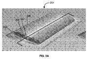
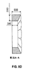
前記下面は、前記材料内に焦点を有する放物曲線を画定し、前記材料は、複数の半導体を含む複数のフィルムを備える、項目1に記載のシステム。
(項目3)
前記フィルムは、アルゴンガスを使用するプロセスによって形成される製品であり、前記フィルムは、層剥離に抵抗する、項目2に記載のシステム。
(項目4)
前記材料と接触し、セルの外側からアクセス可能な第1の電気接点および第2の電気接点を画定する、第1の電極および第2の電極をさらに備える、項目1に記載のシステム。
(項目5)
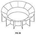
前記上面は、曲面であり、前記曲面は、前記セルが雲のない日に屋外に位置するとき、直射日光が日の出から日の入まで前記曲面の法線を画定するように成形される、項目1に記載のシステム。
(項目6)
赤外EMRへの前記上面の暴露は、前記第1の電気接点および前記第2の電気接点を横断して電圧を生産する、項目5に記載のシステム。
(項目7)
前記セルは、少なくとも約200〜5000EVのスペクトルを横断して前記EMRからエネルギーを捕捉する、項目1に記載のシステム。
(項目8)
前記EMRへの前記上面の暴露は、少なくとも2kW/m 3 を生産する、項目1に記載のシステム。
(項目9)
電力を生産するために、強化リン酸塩、MgF、およびサファイアガラスを含む、UV、可視、および不可視EMRを使用するように動作可能であり、間接EM放射エネルギーを吸収するために、角度付けられた銀めっき頂点のプリズムをさらに備える、項目1に記載のシステム。
(項目10)
少なくとも約3つのEMアルゴンフィルムを備える、項目1に記載のシステム。
(項目11)
前記EMアルゴンフィルムは、透明かつ安定しており、少なくとも約200ev〜5000evを吸収することが可能である、項目10に記載のシステム。
(項目12)
屈折された前記EMRの6〜8%を下回る合計EMRスペクトルを吸収するように動作可能である、項目1に記載のシステム。
(項目13)
二重放物線反射基部をさらに備える、項目1に記載のシステム。
(項目14)
中への放射を可能にするが、その退出を阻害する半透過性膜として作用することによって、前記EMRを分散し、吸収を増加させる、内部ライニングをさらに備える、項目1に記載のシステム。
(項目15)
プリズム集束が、表面積を2倍に増加させる、項目1に記載のシステム。
(項目16)
EMRの光子が、平均して、少なくとも約7回前記材料を通過し、前記EMRの光子の少なくとも一部は、およそ37回前記材料を通過するように、前記材料を通して戻るようにEMRを押勢する、放物線鏡面を底面に備える、項目1に記載のシステム。
(項目17)
電力を生成するためのプロセスであって、
複数のバンドギャップによって画定される、材料内に構成される高密度充填材料リボンを有する3次元空間を画定する、上面および下面を伴う材料の本体と、電気エネルギーを生産するためにそれと接触する少なくとも1つの電極とを供給するステップと、
EM放射を受信するステップと、
花弁状幾何学構成を有する電磁捕捉システム(EM−CS)内で、前記EM放射内のエネルギーの55%を上回るものを電気エネルギーに変換するステップと、
を含む、プロセス。
(項目18)
前記EM−CSはさらに、前記システムの効率が最大限にされるように、日光を指向および捕捉する二重放物線反射基部を備え、それによって、プリズムコンセントレータが追加されると、これは、2倍のエネルギー面積と同等である暴露を与える複数の変形を追加する、項目17に記載のプロセス。
(項目19)
前記EM−CSはさらに、最高点および区域に応じて、より多くの吸収される合計kW/日を与える、少なくとも約500パーセントのさらなるEM放射までを捕捉する能力を有するシステムを備える、項目18に記載のプロセス。
(項目20)
前記EM−CSはさらに、捕捉側面を有する標準EMパネルおよびアセンブリを備え、それによって、内部ライニングは、中への放射を可能にするが、その退出を阻害する半透過性膜として作用し、EM放射を分散し、吸収を増加させる、項目19に記載のプロセス。
(項目21)
従来の光起電性パネルまたはフィルム単独よりも、最大66%の合計放射の増加に効果的なEM−CSをさらに備える、項目19に記載のプロセス。
(項目22)
直接、間接、反射、プリズム、および拡散されたエネルギーを吸収する能力を有する一方、ルーチン保守のみで経時的に動作的に機能するシステムをさらに備える、項目21に記載のプロセスまたは本明細書のいずれかの他の項目による製品。
Claims (22)
- 改良された高効率電磁エネルギー捕捉システム(EM−CS)であって、前記システムは、組み合わせて、
上面層および下面層を備える材料の少なくとも1つの本体を備え、それによって、前記上面層は、前記材料への電磁放射(EMR)を受信し、
前記上面層および下面層は、内部EMRを前記材料に戻すように反射し、
前記材料は、実質的に、前記上面層と前記下面層との間の空間の3次元に及び、それによって、前記内部EMRは、前記3次元内の材料と相互作用し、
前記材料は、複数のバンドギャップによって画定される高密度充填リボン技術を用いて、その中に進行するEMRを捕捉し、それによって、前記内部EMRは、電子を価電子帯から伝導帯に励起し、
少なくとも1つの電極が、前記材料と接触し、電気エネルギーを提供し、それによって、EV範囲から吸収されたエネルギーの50を上回る効率が、達成される、システム。 - 前記下面は、前記材料内に焦点を有する放物曲線を画定し、前記材料は、複数の半導体を含む複数のフィルムを備える、請求項1に記載のシステム。
- 前記フィルムは、アルゴンガスを使用するプロセスによって形成される製品であり、前記フィルムは、層剥離に抵抗する、請求項2に記載のシステム。
- 前記材料と接触し、セルの外側からアクセス可能な第1の電気接点および第2の電気接点を画定する、第1の電極および第2の電極をさらに備える、請求項1に記載のシステム。
- 前記上面は、曲面であり、前記曲面は、前記セルが雲のない日に屋外に位置するとき、直射日光が日の出から日の入まで前記曲面の法線を画定するように成形される、請求項1に記載のシステム。
- 赤外EMRへの前記上面の暴露は、前記第1の電気接点および前記第2の電気接点を横断して電圧を生産する、請求項5に記載のシステム。
- 前記セルは、少なくとも約200〜5000EVのスペクトルを横断して前記EMRからエネルギーを捕捉する、請求項1に記載のシステム。
- 前記EMRへの前記上面の暴露は、少なくとも2kW/m3を生産する、請求項1に記載のシステム。
- 電力を生産するために、強化リン酸塩、MgF、およびサファイアガラスを含む、UV、可視、および不可視EMRを使用するように動作可能であり、間接EM放射エネルギーを吸収するために、角度付けられた銀めっき頂点のプリズムをさらに備える、請求項1に記載のシステム。
- 少なくとも約3つのEMアルゴンフィルムを備える、請求項1に記載のシステム。
- 前記EMアルゴンフィルムは、透明かつ安定しており、少なくとも約200ev〜5000evを吸収することが可能である、請求項10に記載のシステム。
- 屈折された前記EMRの6〜8%を下回る合計EMRスペクトルを吸収するように動作可能である、請求項1に記載のシステム。
- 二重放物線反射基部をさらに備える、請求項1に記載のシステム。
- 中への放射を可能にするが、その退出を阻害する半透過性膜として作用することによって、前記EMRを分散し、吸収を増加させる、内部ライニングをさらに備える、請求項1に記載のシステム。
- プリズム集束が、表面積を2倍に増加させる、請求項1に記載のシステム。
- EMRの光子が、平均して、少なくとも約7回前記材料を通過し、前記EMRの光子の少なくとも一部は、およそ37回前記材料を通過するように、前記材料を通して戻るようにEMRを押勢する、放物線鏡面を底面に備える、請求項1に記載のシステム。
- 電力を生成するためのプロセスであって、
複数のバンドギャップによって画定される、材料内に構成される高密度充填材料リボンを有する3次元空間を画定する、上面および下面を伴う材料の本体と、電気エネルギーを生産するためにそれと接触する少なくとも1つの電極とを供給するステップと、
EM放射を受信するステップと、
花弁状幾何学構成を有する電磁捕捉システム(EM−CS)内で、前記EM放射内のエネルギーの55%を上回るものを電気エネルギーに変換するステップと、
を含む、プロセス。 - 前記EM−CSはさらに、前記システムの効率が最大限にされるように、日光を指向および捕捉する二重放物線反射基部を備え、それによって、プリズムコンセントレータが追加されると、これは、2倍のエネルギー面積と同等である暴露を与える複数の変形を追加する、請求項17に記載のプロセス。
- 前記EM−CSはさらに、最高点および区域に応じて、より多くの吸収される合計kW/日を与える、少なくとも約500パーセントのさらなるEM放射までを捕捉する能力を有するシステムを備える、請求項18に記載のプロセス。
- 前記EM−CSはさらに、捕捉側面を有する標準EMパネルおよびアセンブリを備え、それによって、内部ライニングは、中への放射を可能にするが、その退出を阻害する半透過性膜として作用し、EM放射を分散し、吸収を増加させる、請求項19に記載のプロセス。
- 従来の光起電性パネルまたはフィルム単独よりも、最大66%の合計放射の増加に効果的なEM−CSをさらに備える、請求項19に記載のプロセス。
- 直接、間接、反射、プリズム、および拡散されたエネルギーを吸収する能力を有する一方、ルーチン保守のみで経時的に動作的に機能するシステムをさらに備える、請求項21に記載のプロセスまたは本明細書のいずれかの他の請求項による製品。
Applications Claiming Priority (5)
| Application Number | Priority Date | Filing Date | Title |
|---|---|---|---|
| US201462002122P | 2014-05-22 | 2014-05-22 | |
| US62/002,122 | 2014-05-22 | ||
| US201462024305P | 2014-07-14 | 2014-07-14 | |
| US62/024,305 | 2014-07-14 | ||
| PCT/US2015/032148 WO2015179745A1 (en) | 2014-05-22 | 2015-05-22 | Full spectrum electro-magnetic energy system |
Related Child Applications (1)
| Application Number | Title | Priority Date | Filing Date |
|---|---|---|---|
| JP2018055314A Division JP2018113472A (ja) | 2014-05-22 | 2018-03-22 | フルスペクトル電磁エネルギーシステム |
Publications (1)
| Publication Number | Publication Date |
|---|---|
| JP2017517156A true JP2017517156A (ja) | 2017-06-22 |
Family
ID=54554823
Family Applications (2)
| Application Number | Title | Priority Date | Filing Date |
|---|---|---|---|
| JP2016574459A Pending JP2017517156A (ja) | 2014-05-22 | 2015-05-22 | フルスペクトル電磁エネルギーシステム |
| JP2018055314A Pending JP2018113472A (ja) | 2014-05-22 | 2018-03-22 | フルスペクトル電磁エネルギーシステム |
Family Applications After (1)
| Application Number | Title | Priority Date | Filing Date |
|---|---|---|---|
| JP2018055314A Pending JP2018113472A (ja) | 2014-05-22 | 2018-03-22 | フルスペクトル電磁エネルギーシステム |
Country Status (16)
| Country | Link |
|---|---|
| EP (1) | EP3146617B1 (ja) |
| JP (2) | JP2017517156A (ja) |
| KR (1) | KR101893843B1 (ja) |
| CN (1) | CN106464198B (ja) |
| AP (1) | AP2016009625A0 (ja) |
| AU (4) | AU2015263966A1 (ja) |
| BR (1) | BR112016027361A8 (ja) |
| CA (1) | CA2959192C (ja) |
| ES (1) | ES2791175T3 (ja) |
| GB (1) | GB2540309B (ja) |
| IL (1) | IL248631A (ja) |
| MX (1) | MX356379B (ja) |
| PL (1) | PL3146617T3 (ja) |
| RU (1) | RU2689144C2 (ja) |
| SG (1) | SG11201609720QA (ja) |
| WO (1) | WO2015179745A1 (ja) |
Families Citing this family (4)
| Publication number | Priority date | Publication date | Assignee | Title |
|---|---|---|---|---|
| US11509264B2 (en) | 2014-05-22 | 2022-11-22 | Solar Cubed Holdings Llc | Full spectrum electro-magnetic energy system |
| EA036207B1 (ru) * | 2019-08-07 | 2020-10-14 | Федеральное государственное автономное образовательное учреждение высшего образования "Санкт-Петербургский государственный электротехнический университет "ЛЭТИ" им. В.И. Ульянова (Ленина)" (СПбГЭТУ "ЛЭТИ") | Солнечный элемент со спектральным разделением солнечного излучения |
| CN115407046B (zh) * | 2022-08-05 | 2024-04-16 | 西南石油大学 | 基于岩石细观结构与等效石英含量的研磨性综合表征方法 |
| CN118136710B (zh) * | 2024-04-02 | 2024-08-13 | 江苏新源太阳能科技有限公司 | 一种光伏组件 |
Citations (3)
| Publication number | Priority date | Publication date | Assignee | Title |
|---|---|---|---|---|
| JP2007189025A (ja) * | 2006-01-12 | 2007-07-26 | Sharp Corp | 多接合型太陽電池 |
| WO2013059708A2 (en) * | 2011-10-21 | 2013-04-25 | University Of Utah Research Foundation | Homogeneous multiple band gap devices |
| JP2013172072A (ja) * | 2012-02-22 | 2013-09-02 | Nippon Telegr & Teleph Corp <Ntt> | 2接合太陽電池 |
Family Cites Families (22)
| Publication number | Priority date | Publication date | Assignee | Title |
|---|---|---|---|---|
| ES2023332A6 (es) * | 1990-07-23 | 1992-01-01 | Univ Madrid Politecnica | Cavidad confinadora de luz con limitacion anguloespacial del haz emergente. |
| US5646397A (en) * | 1991-10-08 | 1997-07-08 | Unisearch Limited | Optical design for photo-cell |
| US5590031A (en) * | 1994-07-27 | 1996-12-31 | Mead, Jr.; Franklin B. | System for converting electromagnetic radiation energy to electrical energy |
| US6425391B1 (en) * | 2001-05-23 | 2002-07-30 | Jeffrey A. Davoren | Electromagnetic radiation collector system |
| US6689949B2 (en) * | 2002-05-17 | 2004-02-10 | United Innovations, Inc. | Concentrating photovoltaic cavity converters for extreme solar-to-electric conversion efficiencies |
| US7619159B1 (en) * | 2002-05-17 | 2009-11-17 | Ugur Ortabasi | Integrating sphere photovoltaic receiver (powersphere) for laser light to electric power conversion |
| US8344238B2 (en) * | 2005-07-19 | 2013-01-01 | Solyndra Llc | Self-cleaning protective coatings for use with photovoltaic cells |
| US7741557B2 (en) * | 2005-12-19 | 2010-06-22 | Corning Incorporated | Apparatus for obtaining radiant energy |
| US8283554B2 (en) * | 2005-12-19 | 2012-10-09 | Corning Incorporated | Method and apparatus for concentrating light |
| NL1031544C2 (nl) * | 2006-04-07 | 2007-10-09 | Suncycle B V | Inrichting voor het omzetten van zonne-energie. |
| RU2359396C1 (ru) * | 2007-09-25 | 2009-06-20 | Николай Александрович Татаринов | Устройство получения электрической энергии |
| JP2011508430A (ja) * | 2007-12-21 | 2011-03-10 | クォルコム・メムズ・テクノロジーズ・インコーポレーテッド | 多接合光起電力セル |
| KR20100009323A (ko) * | 2008-07-18 | 2010-01-27 | 삼성전자주식회사 | 벌브 타입 집광형 태양전지 모듈 |
| CN101355327A (zh) * | 2008-09-16 | 2009-01-28 | 刘志勇 | 全方向太阳光球形聚光器 |
| JP4993021B2 (ja) * | 2008-11-19 | 2012-08-08 | 凸版印刷株式会社 | 光再利用シート及び太陽電池モジュール |
| WO2012037379A2 (en) * | 2010-09-15 | 2012-03-22 | Solarity, Inc. | Single and multi-junction light and carrier collection management cells |
| US8163581B1 (en) * | 2010-10-13 | 2012-04-24 | Monolith IC 3D | Semiconductor and optoelectronic devices |
| US20120186635A1 (en) * | 2011-01-26 | 2012-07-26 | Eastman Craig D | High efficiency electromagnetic radiation collection method and device |
| KR102033046B1 (ko) * | 2011-12-09 | 2019-10-16 | 레드웨이브 에너지, 인코포레이티드 | 전자기 방사를 전기 에너지로 변환하는 시스템 및 방법 |
| IL217059A (en) * | 2011-12-18 | 2015-07-30 | Or Hama Energy Ltd | Lightweight system and method for dynamic solar energy utilization |
| US8471142B1 (en) * | 2012-08-16 | 2013-06-25 | Pu Ni Tai Yang Neng (Hangzhou) Co., Limited | Solar energy systems using external reflectors |
| CN103595338A (zh) * | 2013-10-24 | 2014-02-19 | 河海大学 | 一种光热一体化温室气体发电装置 |
-
2015
- 2015-05-22 WO PCT/US2015/032148 patent/WO2015179745A1/en active Application Filing
- 2015-05-22 AP AP2016009625A patent/AP2016009625A0/en unknown
- 2015-05-22 ES ES15796356T patent/ES2791175T3/es active Active
- 2015-05-22 JP JP2016574459A patent/JP2017517156A/ja active Pending
- 2015-05-22 RU RU2016150498A patent/RU2689144C2/ru active
- 2015-05-22 EP EP15796356.2A patent/EP3146617B1/en active Active
- 2015-05-22 KR KR1020167035980A patent/KR101893843B1/ko active IP Right Grant
- 2015-05-22 BR BR112016027361A patent/BR112016027361A8/pt active Search and Examination
- 2015-05-22 MX MX2016014285A patent/MX356379B/es active IP Right Grant
- 2015-05-22 SG SG11201609720QA patent/SG11201609720QA/en unknown
- 2015-05-22 GB GB1618375.8A patent/GB2540309B/en not_active Expired - Fee Related
- 2015-05-22 CA CA2959192A patent/CA2959192C/en active Active
- 2015-05-22 CN CN201580030926.8A patent/CN106464198B/zh not_active Expired - Fee Related
- 2015-05-22 AU AU2015263966A patent/AU2015263966A1/en not_active Abandoned
- 2015-05-22 PL PL15796356T patent/PL3146617T3/pl unknown
-
2016
- 2016-10-31 IL IL248631A patent/IL248631A/en active IP Right Grant
-
2018
- 2018-02-23 AU AU2018201320A patent/AU2018201320A1/en not_active Abandoned
- 2018-03-22 JP JP2018055314A patent/JP2018113472A/ja active Pending
-
2020
- 2020-04-30 AU AU2020202888A patent/AU2020202888A1/en not_active Abandoned
-
2021
- 2021-07-16 AU AU2021205103A patent/AU2021205103A1/en not_active Abandoned
Patent Citations (3)
| Publication number | Priority date | Publication date | Assignee | Title |
|---|---|---|---|---|
| JP2007189025A (ja) * | 2006-01-12 | 2007-07-26 | Sharp Corp | 多接合型太陽電池 |
| WO2013059708A2 (en) * | 2011-10-21 | 2013-04-25 | University Of Utah Research Foundation | Homogeneous multiple band gap devices |
| JP2013172072A (ja) * | 2012-02-22 | 2013-09-02 | Nippon Telegr & Teleph Corp <Ntt> | 2接合太陽電池 |
Also Published As
| Publication number | Publication date |
|---|---|
| SG11201609720QA (en) | 2016-12-29 |
| CA2959192A1 (en) | 2015-11-26 |
| AP2016009625A0 (en) | 2016-12-31 |
| PL3146617T3 (pl) | 2020-08-10 |
| RU2689144C2 (ru) | 2019-05-24 |
| GB2540309A (en) | 2017-01-11 |
| RU2016150498A (ru) | 2018-06-22 |
| EP3146617A1 (en) | 2017-03-29 |
| MX2016014285A (es) | 2017-05-30 |
| AU2020202888A1 (en) | 2020-05-21 |
| CN106464198B (zh) | 2019-09-06 |
| ES2791175T3 (es) | 2020-11-03 |
| IL248631A (en) | 2017-06-29 |
| EP3146617B1 (en) | 2020-02-12 |
| BR112016027361A8 (pt) | 2022-08-09 |
| MX356379B (es) | 2018-05-25 |
| EP3146617A4 (en) | 2018-02-28 |
| WO2015179745A1 (en) | 2015-11-26 |
| AU2021205103A1 (en) | 2021-08-12 |
| RU2016150498A3 (ja) | 2018-06-22 |
| CN106464198A (zh) | 2017-02-22 |
| JP2018113472A (ja) | 2018-07-19 |
| AU2015263966A1 (en) | 2016-11-17 |
| GB2540309B (en) | 2017-08-23 |
| CA2959192C (en) | 2017-10-03 |
| KR20170023006A (ko) | 2017-03-02 |
| GB201618375D0 (en) | 2016-12-14 |
| AU2018201320A1 (en) | 2018-03-15 |
| KR101893843B1 (ko) | 2018-09-04 |
| BR112016027361A2 (ja) | 2017-08-15 |
Similar Documents
| Publication | Publication Date | Title |
|---|---|---|
| US8198530B2 (en) | Method and means for a high power solar cell | |
| US20170012155A1 (en) | System and method for manipulating solar energy | |
| US20100212717A1 (en) | Solar collector with optical waveguide | |
| US9256018B2 (en) | Stimulated emission luminescent light-guide solar concentrators | |
| AU2021205103A1 (en) | Full spectrum electro-magnetic energy system | |
| US10608134B2 (en) | Solar power system using hybrid trough and photovoltaic two-stage light concentration | |
| JP2009545182A (ja) | 高効率太陽電池 | |
| US9082911B2 (en) | Three-dimensional metamaterial device with photovoltaic bristles | |
| CA2729611A1 (en) | Solar energy production system | |
| CN101894875B (zh) | 一种高效聚光式太阳能光电转换器 | |
| US11509264B2 (en) | Full spectrum electro-magnetic energy system | |
| US20110259421A1 (en) | Photovoltaic module having concentrator | |
| Omelyanovich | Affordable light-trapping metamaterials for thin-film photovoltaic cells | |
| JP2015038921A (ja) | 光電変換素子 |
Legal Events
| Date | Code | Title | Description |
|---|---|---|---|
| A521 | Request for written amendment filed |
Free format text: JAPANESE INTERMEDIATE CODE: A523 Effective date: 20161220 |
|
| A621 | Written request for application examination |
Free format text: JAPANESE INTERMEDIATE CODE: A621 Effective date: 20161220 |
|
| A871 | Explanation of circumstances concerning accelerated examination |
Free format text: JAPANESE INTERMEDIATE CODE: A871 Effective date: 20161220 |
|
| A975 | Report on accelerated examination |
Free format text: JAPANESE INTERMEDIATE CODE: A971005 Effective date: 20170420 |
|
| A131 | Notification of reasons for refusal |
Free format text: JAPANESE INTERMEDIATE CODE: A131 Effective date: 20170428 |
|
| A02 | Decision of refusal |
Free format text: JAPANESE INTERMEDIATE CODE: A02 Effective date: 20171122 |
|
| A521 | Request for written amendment filed |
Free format text: JAPANESE INTERMEDIATE CODE: A523 Effective date: 20180322 |
|
| A521 | Request for written amendment filed |
Free format text: JAPANESE INTERMEDIATE CODE: A821 Effective date: 20180501 |
|
| A911 | Transfer to examiner for re-examination before appeal (zenchi) |
Free format text: JAPANESE INTERMEDIATE CODE: A911 Effective date: 20180523 |
|
| A912 | Re-examination (zenchi) completed and case transferred to appeal board |
Free format text: JAPANESE INTERMEDIATE CODE: A912 Effective date: 20180615 |
|
| A601 | Written request for extension of time |
Free format text: JAPANESE INTERMEDIATE CODE: A601 Effective date: 20190416 |