JP2017517156A - Full spectrum electromagnetic energy system - Google Patents
Full spectrum electromagnetic energy system Download PDFInfo
- Publication number
- JP2017517156A JP2017517156A JP2016574459A JP2016574459A JP2017517156A JP 2017517156 A JP2017517156 A JP 2017517156A JP 2016574459 A JP2016574459 A JP 2016574459A JP 2016574459 A JP2016574459 A JP 2016574459A JP 2017517156 A JP2017517156 A JP 2017517156A
- Authority
- JP
- Japan
- Prior art keywords
- emr
- energy
- cell
- radiation
- capture
- Prior art date
- Legal status (The legal status is an assumption and is not a legal conclusion. Google has not performed a legal analysis and makes no representation as to the accuracy of the status listed.)
- Pending
Links
- 238000001228 spectrum Methods 0.000 title claims abstract description 36
- 239000000463 material Substances 0.000 claims description 129
- 230000005670 electromagnetic radiation Effects 0.000 claims description 82
- 238000000034 method Methods 0.000 claims description 50
- 239000011521 glass Substances 0.000 claims description 42
- 230000008569 process Effects 0.000 claims description 27
- 230000005855 radiation Effects 0.000 claims description 25
- XKRFYHLGVUSROY-UHFFFAOYSA-N Argon Chemical compound [Ar] XKRFYHLGVUSROY-UHFFFAOYSA-N 0.000 claims description 24
- 238000005516 engineering process Methods 0.000 claims description 22
- 238000010521 absorption reaction Methods 0.000 claims description 13
- 229910052786 argon Inorganic materials 0.000 claims description 12
- 239000012528 membrane Substances 0.000 claims description 7
- 239000004065 semiconductor Substances 0.000 claims description 6
- 239000007789 gas Substances 0.000 claims description 5
- 230000032798 delamination Effects 0.000 claims description 4
- 229910019142 PO4 Inorganic materials 0.000 claims description 3
- NBIIXXVUZAFLBC-UHFFFAOYSA-K phosphate Chemical compound [O-]P([O-])([O-])=O NBIIXXVUZAFLBC-UHFFFAOYSA-K 0.000 claims description 3
- 239000010452 phosphate Substances 0.000 claims description 3
- 229910052594 sapphire Inorganic materials 0.000 claims description 3
- 239000010980 sapphire Substances 0.000 claims description 3
- 238000012423 maintenance Methods 0.000 claims 1
- 210000004027 cell Anatomy 0.000 description 80
- 239000010408 film Substances 0.000 description 53
- 239000010410 layer Substances 0.000 description 40
- 239000000203 mixture Substances 0.000 description 11
- 238000006243 chemical reaction Methods 0.000 description 10
- 229910052710 silicon Inorganic materials 0.000 description 8
- WUPHOULIZUERAE-UHFFFAOYSA-N 3-(oxolan-2-yl)propanoic acid Chemical compound OC(=O)CCC1CCCO1 WUPHOULIZUERAE-UHFFFAOYSA-N 0.000 description 7
- MARUHZGHZWCEQU-UHFFFAOYSA-N 5-phenyl-2h-tetrazole Chemical compound C1=CC=CC=C1C1=NNN=N1 MARUHZGHZWCEQU-UHFFFAOYSA-N 0.000 description 7
- KTSFMFGEAAANTF-UHFFFAOYSA-N [Cu].[Se].[Se].[In] Chemical compound [Cu].[Se].[Se].[In] KTSFMFGEAAANTF-UHFFFAOYSA-N 0.000 description 7
- 229910052980 cadmium sulfide Inorganic materials 0.000 description 7
- 238000000576 coating method Methods 0.000 description 7
- 238000013461 design Methods 0.000 description 7
- 230000005611 electricity Effects 0.000 description 7
- 239000000758 substrate Substances 0.000 description 7
- XUIMIQQOPSSXEZ-UHFFFAOYSA-N Silicon Chemical compound [Si] XUIMIQQOPSSXEZ-UHFFFAOYSA-N 0.000 description 6
- 239000011248 coating agent Substances 0.000 description 6
- 238000010586 diagram Methods 0.000 description 6
- 239000010703 silicon Substances 0.000 description 6
- JBRZTFJDHDCESZ-UHFFFAOYSA-N AsGa Chemical compound [As]#[Ga] JBRZTFJDHDCESZ-UHFFFAOYSA-N 0.000 description 5
- 229910001218 Gallium arsenide Inorganic materials 0.000 description 5
- 230000009471 action Effects 0.000 description 5
- 239000010409 thin film Substances 0.000 description 5
- CURLTUGMZLYLDI-UHFFFAOYSA-N Carbon dioxide Chemical compound O=C=O CURLTUGMZLYLDI-UHFFFAOYSA-N 0.000 description 4
- QPLDLSVMHZLSFG-UHFFFAOYSA-N Copper oxide Chemical compound [Cu]=O QPLDLSVMHZLSFG-UHFFFAOYSA-N 0.000 description 4
- 229910002601 GaN Inorganic materials 0.000 description 4
- JMASRVWKEDWRBT-UHFFFAOYSA-N Gallium nitride Chemical compound [Ga]#N JMASRVWKEDWRBT-UHFFFAOYSA-N 0.000 description 4
- BQCADISMDOOEFD-UHFFFAOYSA-N Silver Chemical compound [Ag] BQCADISMDOOEFD-UHFFFAOYSA-N 0.000 description 4
- 230000000694 effects Effects 0.000 description 4
- 230000006870 function Effects 0.000 description 4
- 238000003306 harvesting Methods 0.000 description 4
- 229930195733 hydrocarbon Natural products 0.000 description 4
- 150000002430 hydrocarbons Chemical class 0.000 description 4
- 229910052709 silver Inorganic materials 0.000 description 4
- 239000004332 silver Substances 0.000 description 4
- 239000013598 vector Substances 0.000 description 4
- OKTJSMMVPCPJKN-UHFFFAOYSA-N Carbon Chemical compound [C] OKTJSMMVPCPJKN-UHFFFAOYSA-N 0.000 description 3
- 238000013459 approach Methods 0.000 description 3
- 238000009472 formulation Methods 0.000 description 3
- 239000011159 matrix material Substances 0.000 description 3
- 230000001590 oxidative effect Effects 0.000 description 3
- 230000035515 penetration Effects 0.000 description 3
- 230000003595 spectral effect Effects 0.000 description 3
- 238000001429 visible spectrum Methods 0.000 description 3
- IJGRMHOSHXDMSA-UHFFFAOYSA-N Atomic nitrogen Chemical compound N#N IJGRMHOSHXDMSA-UHFFFAOYSA-N 0.000 description 2
- -1 CulSe2 Chemical compound 0.000 description 2
- 240000002329 Inga feuillei Species 0.000 description 2
- 230000003667 anti-reflective effect Effects 0.000 description 2
- 230000005540 biological transmission Effects 0.000 description 2
- 229910052799 carbon Inorganic materials 0.000 description 2
- 229910002092 carbon dioxide Inorganic materials 0.000 description 2
- 239000001569 carbon dioxide Substances 0.000 description 2
- 230000008859 change Effects 0.000 description 2
- 238000005229 chemical vapour deposition Methods 0.000 description 2
- 239000002131 composite material Substances 0.000 description 2
- 229960004643 cupric oxide Drugs 0.000 description 2
- 229910052732 germanium Inorganic materials 0.000 description 2
- 229910052738 indium Inorganic materials 0.000 description 2
- APFVFJFRJDLVQX-UHFFFAOYSA-N indium atom Chemical compound [In] APFVFJFRJDLVQX-UHFFFAOYSA-N 0.000 description 2
- 238000009434 installation Methods 0.000 description 2
- 150000002500 ions Chemical class 0.000 description 2
- 229910001507 metal halide Inorganic materials 0.000 description 2
- 150000005309 metal halides Chemical class 0.000 description 2
- 238000012986 modification Methods 0.000 description 2
- 230000004048 modification Effects 0.000 description 2
- 230000003287 optical effect Effects 0.000 description 2
- 229920003223 poly(pyromellitimide-1,4-diphenyl ether) Polymers 0.000 description 2
- 229920001721 polyimide Polymers 0.000 description 2
- 238000010248 power generation Methods 0.000 description 2
- 238000012545 processing Methods 0.000 description 2
- 239000011669 selenium Substances 0.000 description 2
- 238000003860 storage Methods 0.000 description 2
- 239000000126 substance Substances 0.000 description 2
- 230000009466 transformation Effects 0.000 description 2
- 238000000411 transmission spectrum Methods 0.000 description 2
- 229910052727 yttrium Inorganic materials 0.000 description 2
- IJJWOSAXNHWBPR-HUBLWGQQSA-N 5-[(3as,4s,6ar)-2-oxo-1,3,3a,4,6,6a-hexahydrothieno[3,4-d]imidazol-4-yl]-n-(6-hydrazinyl-6-oxohexyl)pentanamide Chemical compound N1C(=O)N[C@@H]2[C@H](CCCCC(=O)NCCCCCC(=O)NN)SC[C@@H]21 IJJWOSAXNHWBPR-HUBLWGQQSA-N 0.000 description 1
- 229920002799 BoPET Polymers 0.000 description 1
- 239000004215 Carbon black (E152) Substances 0.000 description 1
- GYHNNYVSQQEPJS-UHFFFAOYSA-N Gallium Chemical compound [Ga] GYHNNYVSQQEPJS-UHFFFAOYSA-N 0.000 description 1
- ZOKXTWBITQBERF-UHFFFAOYSA-N Molybdenum Chemical compound [Mo] ZOKXTWBITQBERF-UHFFFAOYSA-N 0.000 description 1
- 239000005041 Mylar™ Substances 0.000 description 1
- CBENFWSGALASAD-UHFFFAOYSA-N Ozone Chemical compound [O-][O+]=O CBENFWSGALASAD-UHFFFAOYSA-N 0.000 description 1
- OAICVXFJPJFONN-UHFFFAOYSA-N Phosphorus Chemical compound [P] OAICVXFJPJFONN-UHFFFAOYSA-N 0.000 description 1
- 239000004952 Polyamide Substances 0.000 description 1
- 239000004642 Polyimide Substances 0.000 description 1
- BUGBHKTXTAQXES-UHFFFAOYSA-N Selenium Chemical compound [Se] BUGBHKTXTAQXES-UHFFFAOYSA-N 0.000 description 1
- 229920001646 UPILEX Polymers 0.000 description 1
- 238000002083 X-ray spectrum Methods 0.000 description 1
- MDPILPRLPQYEEN-UHFFFAOYSA-N aluminium arsenide Chemical compound [As]#[Al] MDPILPRLPQYEEN-UHFFFAOYSA-N 0.000 description 1
- 239000006117 anti-reflective coating Substances 0.000 description 1
- 238000003491 array Methods 0.000 description 1
- QVGXLLKOCUKJST-UHFFFAOYSA-N atomic oxygen Chemical compound [O] QVGXLLKOCUKJST-UHFFFAOYSA-N 0.000 description 1
- 230000002457 bidirectional effect Effects 0.000 description 1
- 230000015572 biosynthetic process Effects 0.000 description 1
- 239000005388 borosilicate glass Substances 0.000 description 1
- 239000006227 byproduct Substances 0.000 description 1
- 239000003245 coal Substances 0.000 description 1
- 239000000470 constituent Substances 0.000 description 1
- 238000010276 construction Methods 0.000 description 1
- 230000006378 damage Effects 0.000 description 1
- 230000002939 deleterious effect Effects 0.000 description 1
- 238000000151 deposition Methods 0.000 description 1
- 230000008021 deposition Effects 0.000 description 1
- 238000011161 development Methods 0.000 description 1
- 238000009826 distribution Methods 0.000 description 1
- 230000005684 electric field Effects 0.000 description 1
- 238000000295 emission spectrum Methods 0.000 description 1
- 230000007613 environmental effect Effects 0.000 description 1
- 230000003090 exacerbative effect Effects 0.000 description 1
- 238000001125 extrusion Methods 0.000 description 1
- 239000000446 fuel Substances 0.000 description 1
- 229910052733 gallium Inorganic materials 0.000 description 1
- 229910021389 graphene Inorganic materials 0.000 description 1
- 238000010438 heat treatment Methods 0.000 description 1
- 210000003000 inclusion body Anatomy 0.000 description 1
- AMGQUBHHOARCQH-UHFFFAOYSA-N indium;oxotin Chemical compound [In].[Sn]=O AMGQUBHHOARCQH-UHFFFAOYSA-N 0.000 description 1
- 239000011261 inert gas Substances 0.000 description 1
- 238000002329 infrared spectrum Methods 0.000 description 1
- 230000003993 interaction Effects 0.000 description 1
- 230000014759 maintenance of location Effects 0.000 description 1
- WJZHMLNIAZSFDO-UHFFFAOYSA-N manganese zinc Chemical compound [Mn].[Zn] WJZHMLNIAZSFDO-UHFFFAOYSA-N 0.000 description 1
- 238000004519 manufacturing process Methods 0.000 description 1
- 229910052750 molybdenum Inorganic materials 0.000 description 1
- 239000011733 molybdenum Substances 0.000 description 1
- 238000012544 monitoring process Methods 0.000 description 1
- 229910052757 nitrogen Inorganic materials 0.000 description 1
- 239000003921 oil Substances 0.000 description 1
- 230000003647 oxidation Effects 0.000 description 1
- 238000007254 oxidation reaction Methods 0.000 description 1
- 229910052760 oxygen Inorganic materials 0.000 description 1
- 239000001301 oxygen Substances 0.000 description 1
- 238000004806 packaging method and process Methods 0.000 description 1
- 238000012856 packing Methods 0.000 description 1
- 239000002245 particle Substances 0.000 description 1
- 239000005365 phosphate glass Substances 0.000 description 1
- 229910052698 phosphorus Inorganic materials 0.000 description 1
- 239000011574 phosphorus Substances 0.000 description 1
- 238000013082 photovoltaic technology Methods 0.000 description 1
- 238000007747 plating Methods 0.000 description 1
- 229920002647 polyamide Polymers 0.000 description 1
- 238000007639 printing Methods 0.000 description 1
- 239000000047 product Substances 0.000 description 1
- 238000010926 purge Methods 0.000 description 1
- 230000003763 resistance to breakage Effects 0.000 description 1
- 230000004044 response Effects 0.000 description 1
- 230000000717 retained effect Effects 0.000 description 1
- 229910052711 selenium Inorganic materials 0.000 description 1
- 239000002356 single layer Substances 0.000 description 1
- 239000005361 soda-lime glass Substances 0.000 description 1
- HUAUNKAZQWMVFY-UHFFFAOYSA-M sodium;oxocalcium;hydroxide Chemical compound [OH-].[Na+].[Ca]=O HUAUNKAZQWMVFY-UHFFFAOYSA-M 0.000 description 1
- 238000004544 sputter deposition Methods 0.000 description 1
- 238000006467 substitution reaction Methods 0.000 description 1
- 239000002344 surface layer Substances 0.000 description 1
- 238000002211 ultraviolet spectrum Methods 0.000 description 1
- 230000001755 vocal effect Effects 0.000 description 1
Images


Classifications
-
- H—ELECTRICITY
- H02—GENERATION; CONVERSION OR DISTRIBUTION OF ELECTRIC POWER
- H02J—CIRCUIT ARRANGEMENTS OR SYSTEMS FOR SUPPLYING OR DISTRIBUTING ELECTRIC POWER; SYSTEMS FOR STORING ELECTRIC ENERGY
- H02J50/00—Circuit arrangements or systems for wireless supply or distribution of electric power
- H02J50/001—Energy harvesting or scavenging
-
- H—ELECTRICITY
- H01—ELECTRIC ELEMENTS
- H01L—SEMICONDUCTOR DEVICES NOT COVERED BY CLASS H10
- H01L31/00—Semiconductor devices sensitive to infrared radiation, light, electromagnetic radiation of shorter wavelength or corpuscular radiation and specially adapted either for the conversion of the energy of such radiation into electrical energy or for the control of electrical energy by such radiation; Processes or apparatus specially adapted for the manufacture or treatment thereof or of parts thereof; Details thereof
- H01L31/04—Semiconductor devices sensitive to infrared radiation, light, electromagnetic radiation of shorter wavelength or corpuscular radiation and specially adapted either for the conversion of the energy of such radiation into electrical energy or for the control of electrical energy by such radiation; Processes or apparatus specially adapted for the manufacture or treatment thereof or of parts thereof; Details thereof adapted as photovoltaic [PV] conversion devices
- H01L31/06—Semiconductor devices sensitive to infrared radiation, light, electromagnetic radiation of shorter wavelength or corpuscular radiation and specially adapted either for the conversion of the energy of such radiation into electrical energy or for the control of electrical energy by such radiation; Processes or apparatus specially adapted for the manufacture or treatment thereof or of parts thereof; Details thereof adapted as photovoltaic [PV] conversion devices characterised by at least one potential-jump barrier or surface barrier
- H01L31/072—Semiconductor devices sensitive to infrared radiation, light, electromagnetic radiation of shorter wavelength or corpuscular radiation and specially adapted either for the conversion of the energy of such radiation into electrical energy or for the control of electrical energy by such radiation; Processes or apparatus specially adapted for the manufacture or treatment thereof or of parts thereof; Details thereof adapted as photovoltaic [PV] conversion devices characterised by at least one potential-jump barrier or surface barrier the potential barriers being only of the PN heterojunction type
- H01L31/0725—Multiple junction or tandem solar cells
-
- H—ELECTRICITY
- H01—ELECTRIC ELEMENTS
- H01L—SEMICONDUCTOR DEVICES NOT COVERED BY CLASS H10
- H01L31/00—Semiconductor devices sensitive to infrared radiation, light, electromagnetic radiation of shorter wavelength or corpuscular radiation and specially adapted either for the conversion of the energy of such radiation into electrical energy or for the control of electrical energy by such radiation; Processes or apparatus specially adapted for the manufacture or treatment thereof or of parts thereof; Details thereof
- H01L31/02—Details
- H01L31/0232—Optical elements or arrangements associated with the device
- H01L31/02327—Optical elements or arrangements associated with the device the optical elements being integrated or being directly associated to the device, e.g. back reflectors
-
- H—ELECTRICITY
- H01—ELECTRIC ELEMENTS
- H01L—SEMICONDUCTOR DEVICES NOT COVERED BY CLASS H10
- H01L31/00—Semiconductor devices sensitive to infrared radiation, light, electromagnetic radiation of shorter wavelength or corpuscular radiation and specially adapted either for the conversion of the energy of such radiation into electrical energy or for the control of electrical energy by such radiation; Processes or apparatus specially adapted for the manufacture or treatment thereof or of parts thereof; Details thereof
- H01L31/0248—Semiconductor devices sensitive to infrared radiation, light, electromagnetic radiation of shorter wavelength or corpuscular radiation and specially adapted either for the conversion of the energy of such radiation into electrical energy or for the control of electrical energy by such radiation; Processes or apparatus specially adapted for the manufacture or treatment thereof or of parts thereof; Details thereof characterised by their semiconductor bodies
- H01L31/0352—Semiconductor devices sensitive to infrared radiation, light, electromagnetic radiation of shorter wavelength or corpuscular radiation and specially adapted either for the conversion of the energy of such radiation into electrical energy or for the control of electrical energy by such radiation; Processes or apparatus specially adapted for the manufacture or treatment thereof or of parts thereof; Details thereof characterised by their semiconductor bodies characterised by their shape or by the shapes, relative sizes or disposition of the semiconductor regions
- H01L31/035209—Semiconductor devices sensitive to infrared radiation, light, electromagnetic radiation of shorter wavelength or corpuscular radiation and specially adapted either for the conversion of the energy of such radiation into electrical energy or for the control of electrical energy by such radiation; Processes or apparatus specially adapted for the manufacture or treatment thereof or of parts thereof; Details thereof characterised by their semiconductor bodies characterised by their shape or by the shapes, relative sizes or disposition of the semiconductor regions comprising a quantum structures
- H01L31/035227—Semiconductor devices sensitive to infrared radiation, light, electromagnetic radiation of shorter wavelength or corpuscular radiation and specially adapted either for the conversion of the energy of such radiation into electrical energy or for the control of electrical energy by such radiation; Processes or apparatus specially adapted for the manufacture or treatment thereof or of parts thereof; Details thereof characterised by their semiconductor bodies characterised by their shape or by the shapes, relative sizes or disposition of the semiconductor regions comprising a quantum structures the quantum structure being quantum wires, or nanorods
-
- H—ELECTRICITY
- H01—ELECTRIC ELEMENTS
- H01L—SEMICONDUCTOR DEVICES NOT COVERED BY CLASS H10
- H01L31/00—Semiconductor devices sensitive to infrared radiation, light, electromagnetic radiation of shorter wavelength or corpuscular radiation and specially adapted either for the conversion of the energy of such radiation into electrical energy or for the control of electrical energy by such radiation; Processes or apparatus specially adapted for the manufacture or treatment thereof or of parts thereof; Details thereof
- H01L31/04—Semiconductor devices sensitive to infrared radiation, light, electromagnetic radiation of shorter wavelength or corpuscular radiation and specially adapted either for the conversion of the energy of such radiation into electrical energy or for the control of electrical energy by such radiation; Processes or apparatus specially adapted for the manufacture or treatment thereof or of parts thereof; Details thereof adapted as photovoltaic [PV] conversion devices
- H01L31/042—PV modules or arrays of single PV cells
- H01L31/047—PV cell arrays including PV cells having multiple vertical junctions or multiple V-groove junctions formed in a semiconductor substrate
-
- H—ELECTRICITY
- H01—ELECTRIC ELEMENTS
- H01L—SEMICONDUCTOR DEVICES NOT COVERED BY CLASS H10
- H01L31/00—Semiconductor devices sensitive to infrared radiation, light, electromagnetic radiation of shorter wavelength or corpuscular radiation and specially adapted either for the conversion of the energy of such radiation into electrical energy or for the control of electrical energy by such radiation; Processes or apparatus specially adapted for the manufacture or treatment thereof or of parts thereof; Details thereof
- H01L31/04—Semiconductor devices sensitive to infrared radiation, light, electromagnetic radiation of shorter wavelength or corpuscular radiation and specially adapted either for the conversion of the energy of such radiation into electrical energy or for the control of electrical energy by such radiation; Processes or apparatus specially adapted for the manufacture or treatment thereof or of parts thereof; Details thereof adapted as photovoltaic [PV] conversion devices
- H01L31/054—Optical elements directly associated or integrated with the PV cell, e.g. light-reflecting means or light-concentrating means
- H01L31/0547—Optical elements directly associated or integrated with the PV cell, e.g. light-reflecting means or light-concentrating means comprising light concentrating means of the reflecting type, e.g. parabolic mirrors, concentrators using total internal reflection
-
- H—ELECTRICITY
- H01—ELECTRIC ELEMENTS
- H01L—SEMICONDUCTOR DEVICES NOT COVERED BY CLASS H10
- H01L31/00—Semiconductor devices sensitive to infrared radiation, light, electromagnetic radiation of shorter wavelength or corpuscular radiation and specially adapted either for the conversion of the energy of such radiation into electrical energy or for the control of electrical energy by such radiation; Processes or apparatus specially adapted for the manufacture or treatment thereof or of parts thereof; Details thereof
- H01L31/04—Semiconductor devices sensitive to infrared radiation, light, electromagnetic radiation of shorter wavelength or corpuscular radiation and specially adapted either for the conversion of the energy of such radiation into electrical energy or for the control of electrical energy by such radiation; Processes or apparatus specially adapted for the manufacture or treatment thereof or of parts thereof; Details thereof adapted as photovoltaic [PV] conversion devices
- H01L31/054—Optical elements directly associated or integrated with the PV cell, e.g. light-reflecting means or light-concentrating means
- H01L31/0549—Optical elements directly associated or integrated with the PV cell, e.g. light-reflecting means or light-concentrating means comprising spectrum splitting means, e.g. dichroic mirrors
-
- H—ELECTRICITY
- H01—ELECTRIC ELEMENTS
- H01L—SEMICONDUCTOR DEVICES NOT COVERED BY CLASS H10
- H01L31/00—Semiconductor devices sensitive to infrared radiation, light, electromagnetic radiation of shorter wavelength or corpuscular radiation and specially adapted either for the conversion of the energy of such radiation into electrical energy or for the control of electrical energy by such radiation; Processes or apparatus specially adapted for the manufacture or treatment thereof or of parts thereof; Details thereof
- H01L31/04—Semiconductor devices sensitive to infrared radiation, light, electromagnetic radiation of shorter wavelength or corpuscular radiation and specially adapted either for the conversion of the energy of such radiation into electrical energy or for the control of electrical energy by such radiation; Processes or apparatus specially adapted for the manufacture or treatment thereof or of parts thereof; Details thereof adapted as photovoltaic [PV] conversion devices
- H01L31/054—Optical elements directly associated or integrated with the PV cell, e.g. light-reflecting means or light-concentrating means
- H01L31/056—Optical elements directly associated or integrated with the PV cell, e.g. light-reflecting means or light-concentrating means the light-reflecting means being of the back surface reflector [BSR] type
-
- H—ELECTRICITY
- H02—GENERATION; CONVERSION OR DISTRIBUTION OF ELECTRIC POWER
- H02J—CIRCUIT ARRANGEMENTS OR SYSTEMS FOR SUPPLYING OR DISTRIBUTING ELECTRIC POWER; SYSTEMS FOR STORING ELECTRIC ENERGY
- H02J50/00—Circuit arrangements or systems for wireless supply or distribution of electric power
- H02J50/50—Circuit arrangements or systems for wireless supply or distribution of electric power using additional energy repeaters between transmitting devices and receiving devices
-
- Y—GENERAL TAGGING OF NEW TECHNOLOGICAL DEVELOPMENTS; GENERAL TAGGING OF CROSS-SECTIONAL TECHNOLOGIES SPANNING OVER SEVERAL SECTIONS OF THE IPC; TECHNICAL SUBJECTS COVERED BY FORMER USPC CROSS-REFERENCE ART COLLECTIONS [XRACs] AND DIGESTS
- Y02—TECHNOLOGIES OR APPLICATIONS FOR MITIGATION OR ADAPTATION AGAINST CLIMATE CHANGE
- Y02E—REDUCTION OF GREENHOUSE GAS [GHG] EMISSIONS, RELATED TO ENERGY GENERATION, TRANSMISSION OR DISTRIBUTION
- Y02E10/00—Energy generation through renewable energy sources
- Y02E10/50—Photovoltaic [PV] energy
- Y02E10/52—PV systems with concentrators
Landscapes
- Engineering & Computer Science (AREA)
- Power Engineering (AREA)
- Physics & Mathematics (AREA)
- Condensed Matter Physics & Semiconductors (AREA)
- Electromagnetism (AREA)
- General Physics & Mathematics (AREA)
- Computer Hardware Design (AREA)
- Microelectronics & Electronic Packaging (AREA)
- Computer Networks & Wireless Communication (AREA)
- Sustainable Development (AREA)
- Life Sciences & Earth Sciences (AREA)
- Sustainable Energy (AREA)
- Nanotechnology (AREA)
- Materials Engineering (AREA)
- Chemical & Material Sciences (AREA)
- Photovoltaic Devices (AREA)
- Electroluminescent Light Sources (AREA)
- Physical Or Chemical Processes And Apparatus (AREA)
- Electron Tubes For Measurement (AREA)
Abstract
層内の3次元内に収集された電磁(EM)エネルギーは、複数の平面が、最適化されたバンドギャップ構造を用いて動作可能に機能することを可能にし、それによって、統合された変形および重複する3次元電磁フィルムは、システムが、電磁スペクトル全体を横断してエネルギーを収集することを可能にし、本システムは、活用されるべき直接光および間接光の両方を利用する。EM−CSは、世界のエネルギー需要に対処する従来のシステムよりも多くのエネルギーをEMRから捕捉および含有する。Electromagnetic (EM) energy collected in three dimensions within the layer allows multiple planes to operate operatively with an optimized bandgap structure, thereby integrating deformation and Overlapping three-dimensional electromagnetic films allow the system to collect energy across the entire electromagnetic spectrum, and the system utilizes both direct and indirect light to be exploited. EM-CS captures and contains more energy from EMR than traditional systems that address global energy demand.
Description
(関連出願の相互参照)
本願は、2014年5月22日に出願された米国仮特許出願第62/022,122号、2014年7月14日に出願された米国仮特許出願第62/024,305号に対する優先権およびその利益を主張するものであり、これらの米国仮特許出願の全体の内容は、参照により本明細書中に援用される。
(Cross-reference of related applications)
This application claims priority to US Provisional Patent Application No. 62 / 022,122 filed on May 22, 2014, US Provisional Patent Application No. 62 / 024,305 filed on July 14, 2014, and All the contents of these US provisional patent applications are hereby incorporated by reference.
本発明は、電磁放射からエネルギーを捕捉し、消費のためにそのエネルギーを提供するための方法およびデバイスに関する。 The present invention relates to methods and devices for capturing energy from electromagnetic radiation and providing that energy for consumption.
人々は、普及しているが、旧式のエネルギーへのアプローチの結果に悩まされている。人々が自動車を運転する、夜間に読書する、または工場に給電することを所望するとき、その需要に対してエネルギーを供給する際の主題は、地球からある形態の還元炭素を採り出し、これを燃焼することである。石油および石炭のような炭化水素は、均一に分布していないため、本アプローチは、地政学的な不安定性および破壊を引き起こす。炭化水素は供給が限られているため、代替物が見出されない場合、それらの緊張は、さらに悪化するであろう。それらの地政学的緊張が解決され得た場合であっても、その基本的なエネルギー供給のパラダイムは、炭化水素が燃焼され、二酸化炭素を生産する、一方向の化学量論を前提としている。米国環境保護庁からの報告によると、9兆メートルトンを上回る炭素が、毎年大気中に放出されている。 People are popular, but are plagued by the results of an old-fashioned approach to energy. When people want to drive a car, read at night, or power a factory, the subject of supplying energy for that demand is to take some form of reduced carbon from the earth and use it. It is to burn. Since hydrocarbons such as oil and coal are not evenly distributed, this approach causes geopolitical instability and destruction. Since hydrocarbons are limited in supply, their tensions will be exacerbated if alternatives are not found. Even when those geopolitical tensions can be resolved, the basic energy supply paradigm assumes a one-way stoichiometry where hydrocarbons are burned to produce carbon dioxide. According to a report from the US Environmental Protection Agency, more than 9 trillion metric tons of carbon is released into the atmosphere every year.
太陽光等の代替エネルギーが、それらの源が需要を満たすことが可能である場合、役立ち得る。光起電性(PV)ソーラー発電産業における収益は、年間1,000億ドルに達するが、PV技術は、莫大な設備投資を要求し、これは、せいぜい徐々に利益を生むだけである。既存のPVセルは、(せいぜい)1平方メートルあたり約0.200kWを生産する材料のフラットパネルとして展開されている。晴れた日には、カードテーブルのサイズのソーラーセルは、太陽が照っている限り、6つの電球を点灯させ続け得る。PVセルのある背景に関して、Heringによる米国特許第8,093,492号およびOrtabasiによる米国特許第6,689,949号を参照されたい。 Alternative energy, such as sunlight, can be helpful if those sources are able to meet demand. Revenue in the photovoltaic (PV) solar power industry reaches $ 100 billion annually, but PV technology requires enormous capital investment, which at best only yields profits. Existing PV cells are deployed as flat panels of materials that produce (at best) about 0.200 kW per square meter. On a clear day, a card table size solar cell can keep the six bulbs on as long as the sun is shining. See US Pat. No. 8,093,492 by Hering and US Pat. No. 6,689,949 by Ortabasi for some background on PV cells.
本発明は、電磁放射(EMR)からエネルギーを捕捉し、そのエネルギーを電気として提供し得るセルを提供する。セルは、従来のシステムよりも広いスペクトルのEMR、すなわち、紫外線から赤外線を超えて延在するEV範囲からエネルギーを捕捉する。セルは、EMRが3つの独立した次元を横断してエネルギーを付与するという識見を利用して、3次元の空間を横断してEMRと相互作用する材料の組成物を含み、第1の次元は、磁場Bの変化の方向、第2の次元は、電場Eの変化、第3の次元は、EMRの伝搬の方向によって画定される。内向きのリフレクタを使用することによって、セルは、EMRを内部に捕捉する。3D媒体を使用することによって、セルは、EMRとのその潜在的な相互作用およびEMRからエネルギーを捕捉するための潜在性を最大限にする。セルは、複数のバンドギャップを特徴とする材料の組成物を含む。広い電磁スペクトルを横断してからの内部EMRは、それらの材料の電子を価電子帯から伝導帯に活性化し、これは、含まれる電極を使用して電流として採取されることができる。 The present invention provides a cell that can capture energy from electromagnetic radiation (EMR) and provide that energy as electricity. The cell captures energy from a broader spectrum of EMR than conventional systems, ie, the EV range that extends from ultraviolet to infrared. The cell contains a composition of materials that interact with the EMR across a three-dimensional space, utilizing the insight that the EMR energizes across three independent dimensions, the first dimension being The direction of change of the magnetic field B, the second dimension is defined by the change of the electric field E, and the third dimension is defined by the direction of propagation of the EMR. By using an inward-facing reflector, the cell captures the EMR inside. By using 3D media, the cell maximizes its potential interaction with the EMR and the potential for capturing energy from the EMR. The cell includes a composition of materials characterized by a plurality of band gaps. Internal EMR after crossing a broad electromagnetic spectrum activates the electrons of those materials from the valence band to the conduction band, which can be sampled as a current using the included electrodes.
吸収面およびプリズム集束を伴う湾曲した上面幾何学形状を含むことによって、セルは、毎日の長い持続時間にわたってであってもEMRエネルギーを捕捉し、実際には、厳密には日光ではないとき、セルは、全ての形態の光、間接、反射、拡散、屈曲、およびプリズムを捕捉する。説明される特徴および現象によって、本発明のセルは、エネルギーが捕捉されるEMRスペクトル、ならびにそのエネルギーの捕捉効率、および1日あたり捕捉持続時間を最大限にする。少なくともそれらの理由から、本発明のセルは、非常に高い効率を呈し、実際には、少なくとも約2.9kWh/m3またはそれを上回る電力を提供し得る。 By including a curved top geometry with an absorptive surface and prism focusing, the cell captures EMR energy even over long daily durations, and in fact, when not strictly sunlight, the cell Captures all forms of light, indirect, reflective, diffuse, bent, and prisms. With the features and phenomena described, the cell of the present invention maximizes the EMR spectrum in which energy is captured, as well as the efficiency of capturing that energy, and the capture duration per day. For at least those reasons, the cells of the present invention exhibit very high efficiency and may actually provide power of at least about 2.9 kWh / m 3 or more.
本発明のセルによって提供される高い効率および電力生産に起因して、エネルギーに対する人々の需要は、化学量論的量の二酸化炭素を生産することなく、かつ炭化水素燃料の不均一な分布の周辺の地政学的緊張を悪化させることなく、満たされ得る。したがって、本発明のシステムおよび方法は、人々の悩みを積もらせることなく、世界のエネルギー需要を満たすためのツールを提供する。本発明のシステムおよび方法を使用して、人々は、夜間に読書し、旅行し、自身のビジネスを運営し、楽しく持続可能な様式で自身の生活を継続し得る。 Due to the high efficiency and power production provided by the cells of the present invention, people's demand for energy is produced without producing stoichiometric amounts of carbon dioxide and around a heterogeneous distribution of hydrocarbon fuels. Can be met without exacerbating the geopolitical tensions of Thus, the system and method of the present invention provides a tool for meeting global energy demands without causing people's troubles. Using the system and method of the present invention, people can read at night, travel, run their business and continue their lives in a fun and sustainable manner.
PVソーラー発電の問題に対処するためのモジュール式技術は、利用可能なエネルギーの電磁スペクトル全体の活用を妨げている、二次元(ユークリッド)アプローチによって現在まで制約を受けていると思量される。要するに、xおよびy軸を使用してPVソーラーエネルギー収集の限界ならびに境界を定義することは、本質的に制限的である。 Modular technology to address the problem of PV solar power generation seems to have been constrained to date by a two-dimensional (Euclidean) approach that has prevented the entire electromagnetic spectrum of available energy from being utilized. In short, defining the limits and boundaries of PV solar energy collection using the x and y axes is inherently limiting.
故に、本発明の目的は、多くのKw/時および1平方メートルあたりの最大エネルギー採取を促進する、高密度充填(リボン技術)を活用する方法論、システム、およびプロセスを提供することである。 Therefore, it is an object of the present invention to provide methodologies, systems, and processes that utilize high density packing (ribbon technology) that facilitates many Kw / hr and maximum energy harvest per square meter.
簡潔に記載すると、層内の3次元に収集された電磁(EM)エネルギーは、複数の平面が、最適化されたバンドギャップ構造を用いて動作可能に機能することを可能にし、それによって、統合された変形および重複する3次元電磁フィルムは、システムが、電磁スペクトル全体を横断してエネルギーを収集することを可能にし、本システムは、活用されるべき直接光および間接光の両方を利用する。 Briefly described, the electromagnetic (EM) energy collected in three dimensions within a layer allows multiple planes to operate operatively using an optimized bandgap structure, thereby integrating The deformed and overlapping three-dimensional electromagnetic films allow the system to collect energy across the entire electromagnetic spectrum, and the system utilizes both direct and indirect light to be exploited.
本発明の側面は、上面層および下面層を伴う材料の本体を含む、電磁エネルギー捕捉セルを提供する。上面層は、材料への電磁放射(EMR)を受信し、上面層および下面層は、内部(EMR)を材料に戻すように反射し、材料は、内部EMRが3次元内の材料と相互作用するように、実質的に、上面と下面との間の空間の3次元に及ぶ。材料の組成物は、可視スペクトルの外側の内部EMRの波長が、電子を価電子帯から伝導帯に励起するように、複数のバンドギャップを画定する。 An aspect of the invention provides an electromagnetic energy capture cell that includes a body of material with a top layer and a bottom layer. The top layer receives electromagnetic radiation (EMR) to the material, the top and bottom layers reflect back to return the interior (EMR) back to the material, and the material interacts with the material in three dimensions. As such, it substantially spans the three dimensions of the space between the top and bottom surfaces. The composition of the material defines a plurality of band gaps such that the wavelength of the internal EMR outside the visible spectrum excites electrons from the valence band to the conduction band.
セルは、材料と接触する少なくとも1つの電極を含む。好ましい実施形態では、下面層は、材料内に焦点を有する放物曲線を画定する。上面層は、例えば、セルが雲のない日に屋外に位置するとき、直射日光が日の出から日の入まで曲面の法線を画定するように、湾曲してもよい。材料は、複数の半導体から成る複数のフィルムを含んでもよい。好ましくは、フィルムは、非平面幾何学形状を画定する。フィルムは、フィルムが層剥離に抵抗するように、アルゴンガスを使用するプロセスによって形成されてもよい。当業者は、厚い/薄いという用語に関わる意味論は、技術的な区別とは対照的に、歴史的なアーチファクトであることを理解する。 The cell includes at least one electrode in contact with the material. In a preferred embodiment, the bottom layer defines a parabolic curve having a focal point in the material. The top layer may be curved so that, for example, when the cell is located outdoors on a cloudless day, direct sunlight defines a curved normal from sunrise to sunset. The material may include a plurality of films composed of a plurality of semiconductors. Preferably, the film defines a non-planar geometry. The film may be formed by a process using argon gas so that the film resists delamination. Those skilled in the art understand that the semantics relating to the term thick / thin are historical artifacts as opposed to technical distinctions.
セルはさらに、材料と接触し、セルの外側からアクセス可能な第1の電気接点および第2の電気接点を画定する、第1の電極および第2の電極を含んでもよい。赤外波長を含むEMRへの上面の暴露は、第1の電気接点および第2の電気接点を横断して電圧を生産する。 The cell may further include a first electrode and a second electrode that contact the material and define a first electrical contact and a second electrical contact accessible from outside the cell. Exposure of the top surface to the EMR containing infrared wavelengths produces a voltage across the first electrical contact and the second electrical contact.
実施形態によると、セルは、広いスペクトルのEMRを電気に変換し、EMRは、紫外線から赤外線を超えた形態を含む。セルは、電力を生産するために、UV、可視、および不可視EMRを使用するように動作可能であってもよい。本発明のセルは、200〜5000EVのスペクトルを網羅する。EMRへの上面の暴露は、少なくとも2kW/m3を生産することが見出され得る。 According to embodiments, the cell converts a broad spectrum of EMR to electricity, which includes forms from ultraviolet to infrared. The cell may be operable to use UV, visible, and invisible EMR to produce power. The cell of the present invention covers a spectrum of 200 to 5000 EV. It can be found that exposure of the top surface to EMR produces at least 2 kW / m 3 .
ある実施形態では、セルは、間接EM放射エネルギーを吸収するために、角度付けられた銀めっき頂点のプリズムを含む。セルは、透明かつ安定しており、200ev〜5000evを吸収することが可能であり得る、複数のEMアルゴンフィルムを含んでもよい。好ましくは、角度付けられた銀めっき頂点のプリズムは、間接EM放射エネルギーを吸収する。セルは、屈折されたEMRの10%を下回る合計EMRスペクトルを吸収してもよい。プリズム集束が、表面積を2倍に増加させてもよい。 In some embodiments, the cell includes an angled silver plated apex prism to absorb indirect EM radiant energy. The cell may include multiple EM argon films that are transparent and stable and may be capable of absorbing from 200 ev to 5000 ev. Preferably, the angled silver plated apex prism absorbs indirect EM radiant energy. The cell may absorb a total EMR spectrum that is less than 10% of the refracted EMR. Prism focusing may increase the surface area by a factor of two.
セルは、1つまたはそれを上回る内部鏡面放物線リフレクタを備える、アセンブリを含んでもよい。セルは、(例えば、材料を通してEMRの光子の内部反射および複数の通過を助長するために)二重放物線反射基部を含んでもよい。セルはまた、中への放射を可能にするが、その退出を阻害する半透過性膜として作用することによって、EMRを分散し、吸収を増加させる、内部ライニングを含んでもよい。いくつかの実施形態では、内部EMRの任意の所与の光子が、少なくとも7回電子と相互作用する。ある実施形態では、内部EMRの光子が、平均して、30回を上回って電子と相互作用する。セルは、EMRの光子が、平均して、少なくとも7回材料を通過し、EMRの光子の少なくとも一部が、少なくとも37回材料を通過するように、材料を通して戻るようにEMRを押勢する、放物線鏡面を底面に備えてもよい。 The cell may include an assembly comprising one or more internal specular parabolic reflectors. The cell may include a double parabolic reflecting base (eg, to facilitate internal reflection and multiple passage of EMR photons through the material). The cell may also include an internal lining that disperses the EMR and increases absorption by acting as a semi-permeable membrane that allows radiation into it but inhibits its exit. In some embodiments, any given photon of the internal EMR interacts with the electron at least 7 times. In some embodiments, the photons of the internal EMR interact with electrons more than 30 times on average. The cell forces the EMR back through the material such that, on average, the EMR photons pass through the material at least 7 times and at least a portion of the EMR photons pass through the material at least 37 times. A parabolic mirror surface may be provided on the bottom surface.
前述の特徴、化学作用、および構造によって、本発明のセルは、UVからIRを超えたフルスペクトルのEMRからエネルギーを採取する。 Due to the aforementioned features, chemistry, and structure, the cell of the present invention harvests energy from the full spectrum EMR from UV to IR.
上面および下面を伴う材料の本体を含む、電磁エネルギー捕捉セルが、本明細書に示される。材料は、挙げられている性質を呈する、化学作用および内部形状を伴うガラスまたは他のそのような材料を含んでもよい。少なくとも下面は、説明されるような放物線集束を提供することができる。セルは、好ましくは、材料への電磁放射(EMR)を受信する上面を有し、上面および下面は、内部(EMR)を材料に戻すように反射し、材料は、内部EMRが3次元内の材料と相互作用するように、実質的に、上面と下面との間の空間の3次元に及ぶ。例えば、発明的プロセスによる(例えば、アルゴンパージプロセスを介して作製された)フィルムの形態における材料の組成物は、可視スペクトルの外側の内部EMRの波長が、電子を価電子帯から伝導帯に励起するように、複数のバンドギャップを画定する。セルは、重複形成を伴う内部構造または幾何学形状、すなわち、本明細書のデータによって示されるように、従来のPVアレイよりも多くの電力を生成するリボン技術または配置エネルギー密度を有する。 Shown herein is an electromagnetic energy capture cell that includes a body of material with an upper surface and a lower surface. The material may include glass or other such material with chemistry and internal shape that exhibits the listed properties. At least the lower surface can provide parabolic focusing as described. The cell preferably has a top surface that receives electromagnetic radiation (EMR) to the material, the top and bottom surfaces reflecting back the interior (EMR) back to the material, and the material has an internal EMR in three dimensions. To interact with the material, it essentially spans the three dimensions of the space between the top and bottom surfaces. For example, a composition of a material in the form of a film by an inventive process (eg, made via an argon purge process), the wavelength of the internal EMR outside the visible spectrum excites electrons from the valence band to the conduction band. As such, a plurality of band gaps are defined. The cells have an internal structure or geometry with overlapping formation, ie, ribbon technology or deployment energy density that produces more power than conventional PV arrays, as shown by the data herein.
本発明は、そのような放射されたエネルギーのスペクトル全体を活用し、電力を生成する、電磁捕捉システムを構成した。 The present invention has constructed an electromagnetic capture system that utilizes the entire spectrum of such radiated energy to generate power.
今日の標準PVが、より狭い範囲の800〜1100EVを網羅する一方、描写される電磁捕捉システム(EM−CS)は、200−5000EVのより広いスペクトルを網羅する。EM−CSは、今日の標準薄フィルムとは対照的に、より動的なアルゴンフィルムを利用する。 While today's standard PV covers a narrower range of 800-1100 EV, the depicted electromagnetic capture system (EM-CS) covers a wider spectrum of 200-5000 EV. EM-CS utilizes a more dynamic argon film as opposed to today's standard thin film.
EM捕捉システム(EM−CS)は、熱捕捉の領域において、紫外線の形態から赤外線(C)を超えた形態の光を含む、広いスペクトルの電磁放射を捕捉および変換する、新しい技術である。 The EM capture system (EM-CS) is a new technology that captures and converts a broad spectrum of electromagnetic radiation, including light in the area of thermal capture, from ultraviolet to infrared (C).
そのようなより広い日中範囲の電磁放射を捕捉する本技術の能力は、「ソーラー」と同一のものではない。増加したシステム効率と結合されたこの増加した範囲は、より長い時間周期にわたってより大きいパネル容量をもたらし、これは、ワットあたりのより低いコストおよびより大きい合計出力をもたらす。 The technology's ability to capture such broader daytime electromagnetic radiation is not the same as “solar”. This increased range combined with increased system efficiency results in greater panel capacity over a longer time period, which results in lower cost per watt and greater total power.
増加したパネル容量は、有意に少ない表面積を要求し、空間が限定される、および/または高価であっても、パネルが設置されることを可能にする。 Increased panel capacity requires significantly less surface area, allowing panels to be installed even when space is limited and / or expensive.
(本願に対して同時に使用される)「含有する」または「捕捉する」技術は、有意に少ない専有面積、設置労力、および付帯設備を要求する、より小さい建設面積ならびに低減されたパネル数に起因して、現在の住宅/商業/公共施設グレードの設置にわたって、有意なコスト節約をもたらす。 “Contains” or “capture” technology (used simultaneously for this application) is due to smaller construction area and reduced panel count, requiring significantly less footprint, installation effort, and incidental equipment Thus providing significant cost savings over current residential / commercial / public facility grade installations.
バッテリーストレージと組み合わせられたEM−CSは、最初の正当な「ベースロード」再生可能エネルギー解決策として機能することができる。 EM-CS combined with battery storage can serve as the first legitimate “base load” renewable energy solution.
グリッド接続システムおよびオフグリッドシステムの両方に対して適しているため、本システムは、全EMスペクトルエネルギーの区切り使用を提供する。 Because it is suitable for both grid-connected and off-grid systems, the system provides a demarcated use of the total EM spectral energy.
実施形態によると、本発明の「パネル」は、市販の全ての他のパネルと異なり、最大2.9kW/m3のより広い範囲の放射を含有/捕捉および変換するように設計される。故に、本発明によると、パネルは、UV、可視、および不可視光スペクトルを使用する。 According to embodiments, the “panels” of the present invention are designed to contain / capture and convert a wider range of radiation up to 2.9 kW / m 3 , unlike all other commercially available panels. Thus, according to the present invention, the panel uses UV, visible and invisible light spectra.
実施形態によると、複数のEM「アルゴンフィルム」(透明かつ安定しており、200ev〜5000evを吸収することが可能である)が、開示される。同様に、専用のガラス調合物が、合計EM放射スペクトル(任意のタイプの最小値から6〜8%の屈折光)を吸収するように設計され、角度付けられた銀めっき頂点のプリズムの追加がさらに、間接EM放射エネルギーを吸収する能力を増加させる。 According to embodiments, a plurality of EM “argon films” (transparent and stable, capable of absorbing 200 ev to 5000 ev) are disclosed. Similarly, a dedicated glass formulation is designed to absorb the total EM emission spectrum (6-8% refracted light from any type of minimum) and the addition of an angled silver plated apex prism Furthermore, it increases the ability to absorb indirect EM radiant energy.
実施形態によると、二重放物線反射基部が、本システムの効率が最大限にされるように、日光に指向し、それを捕捉する。 According to an embodiment, a double parabolic reflecting base directs and captures sunlight so that the efficiency of the system is maximized.
本技術は、最高点および区域に応じて、より多くの吸収される合計kW/日を与える、最大800パーセントのさらなるEM放射を可能にする。 The technology allows for up to 800 percent additional EM radiation, giving more absorbed total kW / day depending on the peak and area.
実施形態によると、内部ライニングは、中への放射を可能にするが、その退出を阻害する半透過性膜として作用し、EM放射を分散し、吸収を増加させる。 According to embodiments, the internal lining allows radiation into but acts as a semi-permeable membrane that inhibits its exit, disperses EM radiation and increases absorption.
新しい技術は、フィルム単独よりも、合計放射を最大66%増加させる。それが、従来技術が開示するような単なる別のソーラーパネルではなく、これがEM「システム」である理由である。 New technology increases total radiation by up to 66% over film alone. That is why it is an EM “system”, not just another solar panel as disclosed by the prior art.
直接、間接、反射、プリズム、さらには拡散されるエネルギーを吸収する能力も、同様に特徴となる。 Direct, indirect, reflective, prismatic and even the ability to absorb diffused energy is similarly characterized.
内部設計が、電子通過を少なくとも約7〜37回に増加させると思量される。 It is envisioned that the internal design increases electron passage to at least about 7-37 times.
EMパネルがEMスペクトルの一部のみを使用する従来のシステムとは、対照的である(現在のパネルは、0.6kW/m2の最大20%における可視スペクトルのみを使用する)。 In contrast to conventional systems where the EM panel uses only a portion of the EM spectrum (the current panel uses only the visible spectrum at up to 20% of 0.6 kW / m 2 ).
本システムは、平均ソーラーパネルの狭い範囲をはるかに超え、UVからIRの大規模に利用可能な範囲をさらに超える、利用可能な電磁放射エネルギーの全てを使用するシステムを設計したことに由来する。本システムは、はるかに大きい放射のスペクトルを吸収するように設計される。 The system comes from designing a system that uses all of the available electromagnetic radiant energy far beyond the narrow range of the average solar panel and even beyond that available on a large scale from UV to IR. The system is designed to absorb a much larger spectrum of radiation.
既存のソーラーパネルは、800〜1100の波長のみを使用する一方、本教示は、はるかに大きい200〜5000の波長を使用する広スペクトル技術を使用する。 Existing solar panels use only wavelengths between 800 and 1100, while the present teachings use broad spectrum technology that uses much larger wavelengths between 200 and 5000.
現在のパネルは、日光を「跳ね返す」一方、新しいEMパネルは、太陽のエネルギーを「捕捉する」、および/またははるかに大きいその分割量を「含有する」。 The current panel "bounces" sunlight, while the new EM panel "captures" solar energy and / or "contains" its much larger fraction.
放射回転設計は、伝統的なモデルよりも最大約70%放射暴露を増加させる。 Radiant rotation design increases radiation exposure by up to about 70% over traditional models.
本設計は、日光の角度、地球の回転、直線増加時間と、反射/屈折光を減少させ、捕捉セルに進入する光放射の量を増加させるより大きい吸収との関係(スネルの法則)を使用する。 This design uses the relationship between sunlight angle, Earth rotation, linear increase time, and greater absorption that reduces reflected / refracted light and increases the amount of light radiation that enters the capture cell (Snell's Law) To do.
加えて、ガラス組成物は、これが間接光を吸収することを可能にする。 In addition, the glass composition allows it to absorb indirect light.
付加的かつ有用な背景が、Takamotoによる「Status of multijunction solar cells and future development」(2009年5月18日〜21日のCS MANTECH CONFERENCE)(Tampa,FL,USA)(4ページ);Heringによる米国特許第8,093,492号;Bachによる米国特許第6,335,480号;およびOrtabasiによる米国特許第6,689,949号(そのそれぞれは、あらゆる目的のために、あたかも本明細書に完全に記載されているかのように、参照することによって明示的に組み込まれる)に見出され得る。 Additional and useful background is “Status of multi-junction solar cells and future development” by Takamoto (CS MANTECH CONFERENCE, May 18-21, 2009) (Tampa, FL, USA) (page 4); US Pat. No. 8,093,492; US Pat. No. 6,335,480 by Bach; and US Pat. No. 6,689,949 by Ortabasi (each of which is hereby incorporated by reference in its entirety for all purposes). , Which is expressly incorporated by reference).
本明細書に開示される技術は、太陽等の源からエネルギーを生成するためのシステムおよび方法を対象とする。開示される技術の実施形態は、広いスペクトルの電磁エネルギーを捕捉し、そのエネルギーを種々の使用のために電気に効率的に変換することが可能であるように構成される。種々の特徴が、電磁エネルギーの効率的な捕捉が、ソーラー電力生成システムの効率を増加させることを可能にするために含まれることができる。例えば、ガラスの一意の形状および組成物が、本システム内の光の進入および捕捉を改良させるために使用されることができ、放物線状または他の同様のリフレクタが、種々の角度で太陽(または他の電磁エネルギーの源)からそのようなソーラーエネルギー等のエネルギーを捕捉するために使用されることができ、種々の異なるバンドギャップにおける光起電性材料の複数の層が、可視光スペクトル内およびそれを超える広いスペクトルの電磁エネルギーを捕捉するために組み合わせられることができる。 The techniques disclosed herein are directed to systems and methods for generating energy from sources such as the sun. Embodiments of the disclosed technology are configured to be able to capture a broad spectrum of electromagnetic energy and efficiently convert that energy into electricity for various uses. Various features can be included to allow efficient capture of electromagnetic energy to increase the efficiency of the solar power generation system. For example, the unique shape and composition of glass can be used to improve light entry and capture within the system, and parabolic or other similar reflectors can be used at various angles to the sun (or Multiple layers of photovoltaic material in a variety of different band gaps can be used to capture energy such as solar energy from other sources of electromagnetic energy) in the visible light spectrum and It can be combined to capture broad spectrum electromagnetic energy beyond that.
本システムの初期プロトタイプは、ガラスまたは他の透明封入体と、異なるバンドギャップ(バンドギャップ材料)を有する1つまたはそれを上回るソーラー変換材料(すなわち、光起電性材料)を使用して生成された、エネルギー変換スタックと、反射光がガラス封入体によって捕捉され、光起電性材料に向かって指向され得るように、そうでなければ封入体に衝突し得ない日光(または太陽からの他の電磁エネルギー)をガラス封入体に再指向させるように構成され得る、リフレクタとを含む。開示される技術のこれらならびに他の特徴および側面が、利用され、種々の組み合わせにおいて組み合わせられ、効率的なエネルギー生成システムを生成することができる。これらの特徴の種々の側面が、実施例を用いて本文書に説明される。種々の実施形態では、光起電性材料を包装するために使用されるガラスは、光起電性材料に到達する、およびそれによって捕捉され得る電磁放射スペクトルの合計量を増加または最大限にするように調合されることができる。 Initial prototypes of the system are generated using glass or other transparent inclusions and one or more solar conversion materials (ie, photovoltaic materials) with different band gaps (band gap materials). In addition, the energy conversion stack and sunlight (or other light from the sun) that would otherwise not be able to strike the enclosure so that the reflected light can be captured by the glass enclosure and directed towards the photovoltaic material. A reflector, which can be configured to redirect electromagnetic energy) to the glass enclosure. These and other features and aspects of the disclosed technology can be utilized and combined in various combinations to produce an efficient energy generation system. Various aspects of these features are described in this document using examples. In various embodiments, the glass used to package the photovoltaic material increases or maximizes the total amount of electromagnetic radiation spectrum that reaches and can be captured by the photovoltaic material. Can be formulated as follows.
ガラスは、その破壊への抵抗性を改良するように強化され、その広い波長透過スペクトルのために望ましい。例えば、種々の実施形態では、強化リン酸塩、MgF、およびサファイアガラスが、およそ400〜2750nmの波長を横断しておよそ80〜90%の透過をもたらす透過スペクトルを提供されることができる。いくつかの実施形態では、ガラスは、およそ200〜5000nmのスペクトルにわたる高パーセンテージの透過を達成することができる。ガラスは、電磁エネルギーの吸収ならびにガラスの屈折率を改変するために、リン化学物質(例えば、20%またはそれを下回るもの、但し、他のドーピングパーセンテージも使用されることができる)を用いてドーピングされることができる。ドーピングは、ドーピングされていないガラスと比較して、太陽からより多いエネルギーがガラス中に受け入れられ、ガラスの表面から反射されるものがより少なくなるように、ガラスの受け入れの効果的な角度を増加させるために行われる。 Glass is tempered to improve its resistance to breakage and is desirable because of its broad wavelength transmission spectrum. For example, in various embodiments, enhanced phosphate, MgF, and sapphire glass can be provided with a transmission spectrum that provides approximately 80-90% transmission across wavelengths of approximately 400-2750 nm. In some embodiments, the glass can achieve a high percentage of transmission across a spectrum of approximately 200-5000 nm. Glass is doped with phosphorus chemicals (eg, 20% or less, but other doping percentages can also be used) to modify the absorption of electromagnetic energy as well as the refractive index of the glass Can be done. Doping increases the effective angle of acceptance of the glass so that more energy from the sun is accepted into the glass and less is reflected off the surface of the glass compared to undoped glass Done to make.
加えて、ガラス包装は、とりわけ、ガラスの外面上の反射防止(AR)コーティングおよびガラスの内面上の酸化コーティングを含めて管理される。反射防止コーティングは、コーティングされていないガラスと比較して、外面からの反射量を低減させるために追加されることができる。内面上の酸化コーティングは、種々の機能を実施するために提供されることができる。例えば、酸化コーティングは、光をその構成スペクトル成分にプリズム的に分割させるために提供されることができる。これは、入射する光が、スペクトル成分に分離され、スペクトル成分が、ガラスの内面から異なる方向に指向されることを可能にする。 In addition, glass packaging is managed, among other things, including an anti-reflective (AR) coating on the outer surface of the glass and an oxide coating on the inner surface of the glass. An anti-reflective coating can be added to reduce the amount of reflection from the outer surface as compared to uncoated glass. Oxidative coatings on the inner surface can be provided to perform various functions. For example, an oxidative coating can be provided to cause light to be prismaticly divided into its constituent spectral components. This allows incident light to be separated into spectral components that are directed in different directions from the inner surface of the glass.
酸化コーティングはまた、中への放射を可能にするが、その退出を阻害する半透過性膜として作用することもできる。これは、材料を通したその最初の通過の際に吸収および変換されない光子の再使用を促進することができる。説明されるような適切なドーピングおよび他の特性を用いて、ガラスに衝突する直接光の58.86%のバンドギャップ材料への送達およびガラスに衝突する間接光の最大30%のバンドギャップ材料への送達を達成する、実施形態が、実装されることができる。これは、浅い角度でガラスに衝突する光が、反射されるのではなく、捕捉され得、次いで、ガラス包装の中心領域内に位置する光起電性バンドギャップ材料に向かって屈折され得るため、達成されることができる。 The oxidative coating can also act as a semi-permeable membrane that allows radiation into it but inhibits its exit. This can facilitate the reuse of photons that are not absorbed and converted during their first pass through the material. With appropriate doping and other properties as described, direct light impinging on glass is delivered to a band gap material of 58.86% and indirect light impinging on the glass to a band gap material of up to 30%. Embodiments that achieve delivery of can be implemented. This is because light impinging on the glass at a shallow angle can be captured rather than reflected and then refracted towards the photovoltaic band gap material located in the central region of the glass package, Can be achieved.
本教示によると、浅い角度でガラスに衝突する光は、反射されるのではなく、捕捉されることができる。この単純な実施例が、図2に例証され、浅い角度で入射する光線は、光起電性エネルギー変換材料のスタックによって受け入れられ、それに向かって屈折される。ガラス筐体の形状は、本システムの効率および本システムによって捕捉され得る電磁スペクトルの範囲を増加させるために、重要である。本形状は、図に示されるものに限定されない。種々の形状のガラス封入体が使用され得るが、いくつかの実施形態では、丸形形状が、電磁エネルギーの源(例えば、太陽、ランプ、または他のエネルギー源)により直接的な角度を提示し、光起電性材料に向けた光の屈折を促進するために使用される。 According to the present teachings, light that strikes the glass at a shallow angle can be captured rather than reflected. This simple example is illustrated in FIG. 2, where light incident at a shallow angle is received by and refracted toward the stack of photovoltaic energy conversion material. The shape of the glass housing is important to increase the efficiency of the system and the range of the electromagnetic spectrum that can be captured by the system. The shape is not limited to that shown in the figure. Although various shapes of glass enclosures can be used, in some embodiments, the round shape presents a direct angle with a source of electromagnetic energy (eg, the sun, a lamp, or other energy source). Used to promote the refraction of light towards the photovoltaic material.
一側面では、本発明は、改良された高効率電磁エネルギー捕捉システム(EM−CS)を提供する。EM−CSは、セル101を含む。
In one aspect, the present invention provides an improved high efficiency electromagnetic energy capture system (EM-CS). The EM-CS includes a
図1は、本発明のセル101を示す。セル101は、コア部材201と、1つまたはそれを上回る端部部材301とを含む。
FIG. 1 shows a
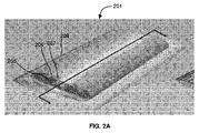
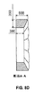
図2A−2Cは、セル101のコア部材201を示す。図2Aは、コア部材201の斜視図を与える。図2Bは、部材201の裁断輪郭図を与える。図2Cは、コア部材201内の電極網を示す。コア部材101は、組み合わせて、少なくとも上面層および下面層を伴う材料本体を含み、それによって、上面層は、材料への電磁放射(EMR)を受信し、上面層および下面層は、内部EMRを材料に戻すように反射する。表面層は、好ましくは、例えば、MgF2もしくは他の好適な金属ハライドを用いてドーピングされたガラスまたはそのような材料(「専用のガラス」)を含む。本体は、上面層と下面層との間の空間の3次元に及び、それによって、内部EMRは、3次元内の材料と相互作用する。本体は、複数のバンドギャップによって画定された高密度充填リボン技術を用いて、その中に進行するEMRを捕捉し、それによって、内部EMRの波長は、電子を価電子帯から伝導帯に励起する。高密度充填リボン技術は、最も内側のフィルム205と、第2のフィルム206と、第3のフィルム207と、最も外側のフィルム208とを含む。好ましい実施形態では、少なくとも約3〜7つのフィルムが、含まれる。一実施形態では、各フィルムは、GaAs、Ge、Si、およびGalnP2から別個に選択されるものを含む。各フィルムは、表1に列挙される材料を別個に含んでもよい。他の実施形態では、GaS、GIP、GIA、InGa、CdTe、CIGS、CdTe/CdS、CulnSe2、GIN、ZMT、および/またはCdS等の材料が、使用されてもよい。図2Cは、本体のフィルムと接触する電極を例証する。本明細書で材料本体の「専用のガラス」と呼ばれる上面は、セル101内のEM放射の保持率を最大限にするために、金属ハライド、好ましくは、MgF2を用いてドーピングされるガラスによって提供されてもよい。ドーピングされる上面は、最も外側のフィルム208であってもよい、すなわち、好ましくは、材料本体の上面の層を被覆する。
2A-2C show the
図3は、セル101の端部部材301を示す。端部部材301は、端部部材601に当接し、基部区分501によって支持される、ハードウェア区分401を含む。図4Aは、ハードウェア区分401の斜視図を与える。図4Bは、ハードウェア区分401の端面図を与える。図4Cは、ハードウェア区分401の上面図を与える。図5Aは、基部区分501の斜視図を与える。図5Bは、基部区分501の端面図を与える。図5Cは、基部区分501の上面図を与える。図6Aは、端部部材601の斜視図を与える。図6Bは、端部部材601の端面図を与える。図6Cは、端部部材601の上面図を与える。
FIG. 3 shows the
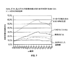
図7は、セル101等のEM−CS捕捉モジュールの効率を示す。本発明の捕捉モジュールは、一方から他方の両方の端部に延在する、下面および湾曲した上面を有する本体を伴う捕捉セルを含み、湾曲した上面は、日の出から日没まで、太陽が空を横断して進行する際に、太陽の光線にほぼ垂直な表面を提供するように輪郭を付けられてもよい。このような幾何学形状は、従来のフラットまたはボックスタイプのソーラーセルを上回って、最大約66%のソーラー暴露の増加を提供し得る。封入体のサイズは、地球に対して非常に小さいため、太陽は、概して、封入体に対して一定の円弧内を進行しないことに留意されたい。いくつかの実施形態では、ガラス筐体は、ガラス筐体の上面を横断するのと比較して、2つの側面により小さい曲率半径を有するように構成されることができる。言い換えると、筐体は、おおよそ花の形状の構成を有するように構成される。
FIG. 7 shows the efficiency of an EM-CS capture module such as
これは、太陽からのエネルギーが地球へと低い傾斜角でガラスに衝突するとき、日の出と日没との間の時間に直接光の捕捉を提供するために有用であり得る。他の実施形態では、ガラス筐体は、太陽が日中に空を横断して移動する際に、太陽の光線に対する法線面を提示するように花弁状形状において構成される。 This can be useful to provide direct light capture at times between sunrise and sunset when energy from the sun strikes the glass at a low tilt angle to the earth. In other embodiments, the glass housing is configured in a petal-like shape to present a normal to the sun's rays as the sun moves across the sky during the day.
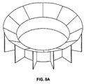
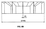
図8A−8Dは、ある実施形態による、厚フィルム/マルチフィルムセル内で使用するための「花弁」部材に関する複合的形状を例証する。図8Aは、花弁的実施形態の斜視図を与える。図8Bは、花弁的実施形態の側面図を与える。図8Cは、花弁的実施形態の上面図を与える。図8Dは、図8Cの線AAに沿った断面図である。図8Aに描写される形態は、図9によって例証されるアルゴリズムの適用を通して導出され、日中の複数の異なる時間からの広いスペクトルの入射するEMのベクトルを、スパッタリング、セレン化、焼鈍、および積層によって生産された厚フィルム状層に対する配向に変形させてもよい。花弁要素のうちの1つまたは複数は、相互に、もしくは広スペクトルEM−CSセルを伴う本明細書に開示される他の要素と併用されてもよい。一実施形態では、本発明は、図8に示されるような少なくとも1つ、好ましくは、少なくとも約3〜7つの部材を含むEM捕捉セルを提供し、各部材は、本明細書のいずれかに列挙されるような含まれる半導体材料によって、少なくとも約1つから多くのバンドギャップを画定する厚フィルムを備える。 8A-8D illustrate a composite shape for a “petal” member for use in a thick film / multifilm cell, according to an embodiment. FIG. 8A provides a perspective view of the petal embodiment. FIG. 8B provides a side view of the petal embodiment. FIG. 8C provides a top view of the petal embodiment. 8D is a cross-sectional view taken along line AA in FIG. 8C. The form depicted in FIG. 8A is derived through the application of the algorithm illustrated by FIG. 9, and broad spectrum incident EM vectors from multiple different times during the day are sputtered, selenized, annealed and stacked. May be deformed to an orientation relative to the thick film-like layer produced by One or more of the petal elements may be used in combination with each other or with other elements disclosed herein with a broad spectrum EM-CS cell. In one embodiment, the present invention provides an EM capture cell comprising at least one, preferably at least about 3-7, members as shown in FIG. Depending on the included semiconductor material as listed, it comprises a thick film that defines at least about one to many band gaps.
複合的な部分的球状形状が、使用されてもよいが、使用される必要はなく、実際には、種々の実施形態では、封入体は、適用の所与の緯度および経度または地理的領域に対する太陽の天体暦に基づいて、太陽により直接的な角度を提示するように成形されることができる。日光モデルおよび他の技法も、ガラス封入体の形状および輪郭を最適化し、最大量のエネルギーを捕捉するために使用されることができる。 A composite partial spherical shape may be used, but need not be used, in fact, in various embodiments, the inclusions are for a given latitude and longitude or geographic region of application. Based on the solar ephemeris, it can be shaped to present a more direct angle to the sun. Sunlight models and other techniques can also be used to optimize the shape and contour of the glass enclosure and capture the maximum amount of energy.
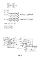
図9は、レンズ製造者の方程式およびスネルの法則の組み合わせの結果を示し、EM−CSに3.5の太陽エネルギーを屈折させ、集束させ、(反射させない)ようにし得ることを示し、外側層は、底部パネルに例証されるベクトルによって示されるような光を図式的に指向させる。 FIG. 9 shows the result of a combination of the lens manufacturer's equation and Snell's law, showing that the EM-CS can be refracted, focused and made (non-reflecting) 3.5 solar energy, Schematically directs light as indicated by the vector illustrated on the bottom panel.
図9は、本発明のセルによる表面幾何学形状の設計を導くための変換公式の使用を例証する。(X,Y,Z)が、世界座標空間における3D点の座標である場合、(u,v)は、ピクセルにおける投影点の座標である。Aは、固有パラメータの行列と呼ばれ、(cx,cy)は、(通常、画像中心にある)主点であり、fx,fyは、ピクセル関連単位で表される焦点距離である。したがって、ユニット内からの画像が、ある倍率によってスケーリングされる場合、これらのパラメータは全て、同一の倍率によってスケーリング(それぞれ、乗算/除算)されるはずである。固有パラメータの行列は、入射する光に依存せず、いったん推定されると、(焦点距離が固定されている限り)再使用されることができる。結合回転並進行列[R|t]は、付帯的パラメータの行列と呼ばれる。これは、セルに対する光源の運動を説明するために使用される。つまり、[R|t]は、点(X,Y,Z)の座標をセルに対して固定されたある座標系に変換する。セルの表面は、ある程度の歪み、主に半径方向の歪みおよびわずかな接線方向の歪みを有し得る。そのため、上記のモデルは、図9に示されるように拡大される。図9では、k_1,k_2,k_3,k_4,k_5,k_6は、半径方向の歪み係数であり、p_1,p_2は、接線方向の歪み係数である。より高次の係数は、考慮されない。示される関数では、係数は、(k_1,k_2,p_1,p_2[,k_3[,k_4,k_5,k_6]])ベクトルとしてパスまたは返される。つまり、ベクトルが4つの要素を含有する場合、これは、k_3=0であることを意味する。歪み係数は、外光に依存せず、したがって、それらもまた、固有セルパラメータに属する。図9に示される拡大されたモデルは、固有および付帯的パラメータを前提として、3D点を画像平面に投影し;固有パラメータ、いくつかの3D点、およびその投影を前提として、付帯的パラメータを算出し;既知の較正パターンのいくつかのビューから(すなわち、セル表面形態の設計のために)固有および付帯的セル光学パラメータを推定し;厚フィルムの相対的な位置および配向を推定し、EM捕捉を最適化する整流変換を算出するために使用されることができる。 FIG. 9 illustrates the use of a transformation formula to guide the design of surface geometry by the cell of the present invention. When (X, Y, Z) is the coordinate of the 3D point in the world coordinate space, (u, v) is the coordinate of the projection point in the pixel. A is called a matrix of eigenparameters, (cx, cy) is the principal point (usually at the center of the image), and fx, fy are focal lengths expressed in pixel-related units. Thus, if an image from within a unit is scaled by a certain magnification, all these parameters should be scaled (multiplied / divided respectively) by the same magnification. The matrix of eigenparameters does not depend on the incident light and can be reused (as long as the focal length is fixed) once estimated. The combined rotation parallel sequence [R | t] is called a matrix of incidental parameters. This is used to describe the movement of the light source relative to the cell. That is, [R | t] converts the coordinates of the point (X, Y, Z) to a certain coordinate system fixed with respect to the cell. The surface of the cell can have some distortion, mainly radial distortion and slight tangential distortion. Therefore, the above model is expanded as shown in FIG. In FIG. 9, k_1, k_2, k_3, k_4, k_5, and k_6 are radial distortion coefficients, and p_1 and p_2 are tangential distortion coefficients. Higher order coefficients are not considered. In the function shown, the coefficients are passed or returned as a (k_1, k_2, p_1, p_2 [, k_3 [, k_4, k_5, k_6]]) vector. That is, if the vector contains 4 elements, this means k_3 = 0. The distortion coefficients do not depend on ambient light, so they also belong to the eigencell parameters. The enlarged model shown in FIG. 9 projects 3D points onto the image plane given the intrinsic and incidental parameters; calculates the incidental parameters given the intrinsic parameters, several 3D points, and their projections. Estimate intrinsic and incidental cell optical parameters from several views of known calibration patterns (ie for cell surface morphology design); estimate relative position and orientation of thick film and capture EM Can be used to calculate a rectification transformation that optimizes.
捕捉セルはさらに、底面および少なくとも一部の上面、例えば、上面の側面に沿って、内部鏡面もしくは銀めっきまたは他の反射性コーティングを備えてもよい。種々の例示的実施形態では、底面全体、ならびに側面のおよそ3分の2の表面は、反射性コーティングまたは鏡面を備えてもよい。内部鏡面は、光子(イオンまたは電子)反射チャンバをもたらし、捕捉セルに進入する電磁放射は、鏡面から反射し、捕捉セルの内側周囲に跳ね返り、全内部反射、またはほぼ全内部反射、もしくは多数の反射を生成し、本システムに進入した光子を含有する。これは、捕捉光子が捕捉セルの内側に分布した光起電性材料に影響を及ぼすであろう可能性を高める効果を有する。 The capture cell may further comprise an internal mirror or silver plating or other reflective coating along the bottom surface and at least a portion of the top surface, eg, the side surface of the top surface. In various exemplary embodiments, the entire bottom surface, as well as approximately two-thirds of the side surfaces, may be provided with a reflective coating or mirror surface. The internal specular provides a photon (ion or electron) reflection chamber, and electromagnetic radiation entering the capture cell reflects off the specular surface and bounces around the inside of the capture cell, causing total internal reflection, or nearly total internal reflection, or multiple It contains a photon that generates a reflection and enters the system. This has the effect of increasing the likelihood that the captured photons will affect the photovoltaic material distributed inside the capture cell.
本実施例の鏡面は、封入体の底面および側面の底部部分に限定されるため、これは、外光の浸透、回折、屈折、または反射に影響を及ぼさず、その唯一の効果は、いったんセル中に浸透した光子の「捕捉」である。光子が捕捉されないままであるとき、これは、最終的に熱に変換され、光起電性材料を加熱する。これは、光子から集積された電子の流動を増加させる(時として、粒子範囲を増加させることによるDelta−K効果と呼ばれる)。 Since the mirror surface of the present embodiment is limited to the bottom surface of the inclusion body and the bottom portion of the side surface, this does not affect the penetration, diffraction, refraction, or reflection of external light, and its only effect is once the cell. This is the “capture” of the photons that have penetrated. When photons remain untrapped, this is eventually converted to heat, heating the photovoltaic material. This increases the flow of electrons accumulated from the photons (sometimes referred to as the Delta-K effect by increasing the particle range).
捕捉セルは、(例えば、ソーダ石灰、ホウケイ酸、またはリン酸塩ガラスの組み合わせの具体的調合を使用して)光学的に活性かつ非反射性の外側を有し、高レベルの光子浸透を可能にしながら、浸透または/地球/太陽光の曲率の角度から生じ得る、回折、屈折、または反射を最小限にし得る。本設計は、大気散乱からのソーラー放射の減衰を可能にし、所与の場所で利用可能なソーラー放射の吸収を増加させる。現在の光起電性システムは、典型的には、薄フィルム光起電性セルを使用し、これは、非常に低い効率を有し、利用可能な光子全体の少量のみを利用し、層剥離に悩まされる。本明細書に説明される技術の種々の実施形態は、光起電性材料のために厚フィルム状技術を利用し、いくつかの実施形態では、これらの厚フィルムは、0.03nmと同程度の薄さまたは5.0ミクロンと同程度の厚さであり得る。 The capture cell has an optically active and non-reflective exterior (eg, using a specific formulation of a combination of soda lime, borosilicate, or phosphate glass), allowing high levels of photon penetration However, diffraction, refraction, or reflection, which can result from penetration or / angle of the earth / sunlight curvature, can be minimized. This design allows for the attenuation of solar radiation from atmospheric scattering and increases the absorption of solar radiation available at a given location. Current photovoltaic systems typically use thin film photovoltaic cells, which have very low efficiency, utilize only a small amount of the total available photons, and delamination Be bothered by. Various embodiments of the technology described herein utilize thick film-like technology for photovoltaic materials, and in some embodiments, these thick films are on the order of 0.03 nm. Or as thin as 5.0 microns.
さらに、議論されるように、薄フィルムまたは厚フィルムの意味は、本明細書に説明されるように、どのバージョンが実装され得るかを当業者が理解するようなものであり、必要に応じて1つまたはそれを上回る通路内に複数の層または複数のバンドギャップ材料の適用を可能にする。例えば、透明カプトン/モリブデン(またはUPILEX等のDuPont(Wilmington,DE,USA)から利用可能な必要とされる他のポリイミド)がある。半透明かつ多レベルのマルチバンドギャップ材料、好ましくは、厚フィルム状材料(またはフィルム205、206等の複数の厚フィルムバンドギャップ格子(MTFBG))が、光起電性材料として提供されてもよい。種々の実施形態では、材料は、それぞれ、異なるバンドギャップを有する異なる半導体材料から作成された複数のp−n接合を伴う、集積化多接合光起電性セルであり得る。他の実施形態では、マルチバンドギャップ材料は、それぞれ、指定されたバンドギャップを伴う光起電性材料を有する、複数の個々の厚フィルムから作製されることができる。理想的には、スタックは、各p−n接合が異なるバンドギャップエネルギーを有し、本デバイスに衝突する電磁スペクトルの異なる波長に応答して、電流を生産するように作製される。これは、より多くの利用可能な電磁スペクトルを使用することによって、本デバイスの変換効率を増加させる。
Further, as discussed, the meaning of thin film or thick film is such that one of ordinary skill in the art will understand which versions can be implemented, as described herein, and as required Allows application of multiple layers or multiple band gap materials in one or more passages. For example, transparent Kapton / molybdenum (or other required polyimides available from DuPont (Wilmington, DE, USA) such as UPILEX). A translucent and multi-level multi-band gap material, preferably a thick film-like material (or a plurality of thick film band gap gratings (MTFBG) such as
複数のバンドギャップを伴う複数の材料を提供することは、ユニットが、複数の異なる波長のスペクトルに応答することを可能にする。いくつかの実施形態では、光起電性スタックは、それぞれ、異なるバンドギャップエネルギーを有する、2〜4層のバンドギャップ材料を含む。他の実施形態では、単一層のスタックまたは4層を上回るものを含む、他の数の層のバンドギャップ材料も、提供されることができる。限界リターンは、例えば、利用可能な電磁エネルギーのスペクトル、スタック内の種々の材料の透明性および吸収効率、捕捉光子を含有するために達成され得る内部反射の量等を含む、いくつかの要因に応じて、層の数が増加するにつれて縮小し得る。動作時、光起電性スタックの外側バンドギャップ材料は、そのバンドギャップエネルギーと関連付けられ得る波長において光子を捕捉し、それらを電流に変換する。 Providing multiple materials with multiple band gaps allows the unit to respond to multiple different wavelength spectra. In some embodiments, the photovoltaic stack comprises 2 to 4 layers of band gap material, each having a different band gap energy. In other embodiments, other numbers of layers of bandgap materials can be provided, including single layer stacks or more than four layers. The marginal return is due to several factors including, for example, the spectrum of available electromagnetic energy, the transparency and absorption efficiency of various materials in the stack, the amount of internal reflection that can be achieved to contain trapped photons, etc. Accordingly, it can shrink as the number of layers increases. In operation, the outer band gap material of the photovoltaic stack captures photons at a wavelength that can be associated with its band gap energy and converts them into current.
第1の層によって捕捉されなかったそれらの光子は、それらが捕捉され、吸収され、後続層の表面から反射されるまで後続層を通過する、またはスタックを通過し、ガラス封入体の反射面から反射される。反射された光子の一部は、光起電性スタックに再び到達し、これらのそうでなければ失われた光子が、捕捉され、電流に変換される機会を提供する。多レベルのマルチバンドギャップ厚フィルムは、屈曲可能であり得、(例えば、紫外線および赤外光を含む)白色光に存在する異なる波長の光に対して、および異なる時間に生じる異なる波長の光に対して最適化された、異なるバンドギャップを有する異なる材料を組み込んでもよい。例えば、日の出および日没の間、光のスペクトルは、真昼のものとは異なるため、それらの異なるタイプの光の可能な限り多くのエネルギーを捕捉するために、異なる材料が、異なるバンドギャップに提供されてもよい。一例示的実施形態では、異なる材料は、例えば、GaAs、Ge、Si、およびGalnP2を含み得る。他の実施形態では、GaS、GIP、GIA、InGa、CdTe、CIGS、CdTe/CdS、CulnSe2、GIN、ZMT、および/またはCdS等の材料が、使用されてもよい。いくつかの実施形態では、材料のバンドギャップは、重複するバンドが存在し、スペクトルの最も高密度な領域からのエネルギー変換を達成するように選択される。いくつかの実施形態では、材料の化学組成物は、接合部のバンドギャップを調整するために変動されることができる。 Those photons that were not captured by the first layer pass through the subsequent layer or pass through the stack until they are captured, absorbed and reflected from the surface of the subsequent layer, from the reflective surface of the glass enclosure. Reflected. Some of the reflected photons reach the photovoltaic stack again, providing an opportunity for these otherwise lost photons to be captured and converted into current. Multi-level multi-band gap thick films can be bendable, for different wavelengths of light present in white light (including, for example, ultraviolet and infrared light), and for different wavelengths of light that occur at different times Different materials with different band gaps, optimized for, may be incorporated. For example, during sunrise and sunset, the spectrum of light is different from that of noon, so different materials provide different band gaps to capture as much energy as possible of those different types of light May be. In one exemplary embodiment, the different materials can include, for example, GaAs, Ge, Si, and GalnP2. In other embodiments, materials such as GaS, GIP, GIA, InGa, CdTe, CIGS, CdTe / CdS, CulSe2, GIN, ZMT, and / or CdS may be used. In some embodiments, the band gap of the material is selected so that overlapping bands exist and achieve energy conversion from the densest region of the spectrum. In some embodiments, the chemical composition of the material can be varied to adjust the band gap of the junction.
表1は、2つまたはそれを上回る層を使用して、それらの関連付けられたバンドギャップおよび推定された変換効率と併用され得る、異なる材料の別の実施例を例証する。当業者は、例示的数字が、重複に起因して、本実施例では低下していることを理解する。 Table 1 illustrates another example of different materials that can be used in conjunction with their associated band gap and estimated conversion efficiency using two or more layers. One skilled in the art will appreciate that the exemplary numbers are reduced in this example due to duplication.

種々の例示的実施形態では、フィルムの両側に光子を集積し得る、2、3、4、または5層の一意の厚フィルム300が、提供されてもよく、そのそれぞれは、ある実施形態では、(例えば、図2Bのフィルム205、206等に示される)約0.03〜5.0ミクロンの厚さに変動し得る。フィルムの長さおよび幅は、封入体の利用可能な寸法および体積に応じて、好適な寸法であり得る。長さおよび幅はまた、フィルムが封入体内に層化される様式に基づいて選定されることもできる。例えば、いくつかの実施形態では、フィルムは、封入体内の平面または平坦(もしくは略平坦)構成において層化されることができる。他の実施形態では、フィルムは、湾曲される、またはカールされる、もしくは被着され、同軸または略同軸方式で封入体内に層化されることができる。例えば、可撓性層は、封入体中に挿入されると、それらが封入体の内側輪郭に従うように、十分な弾性を伴って使用されることができる。故に、フィルムは、封入体の形状をとるように構成されることができる。設計問題が、フィルムの幅を制限すると従来通り見なされる場合、リボン状の長さのフィルムが、封入体の内側で相互に(例えば、螺旋方式で)巻回されることができる。複数層半透明光起電性スタックは、イオン収集のために正電荷と電気的に接続されてもよい。複数層半透明光起電性スタックは、図1、2、および3に関して上記に説明されるように、内部鏡面によって少なくとも部分的に囲繞されてもよい。この一意のフィルム技術は、双方向光起電性経路(すなわち、上から下および下から上へのエネルギー変換)を可能にする。
In various exemplary embodiments, two, three, four, or five unique thick films 300 that can integrate photons on both sides of the film may be provided, each of which, in one embodiment, The thickness may vary from about 0.03 to 5.0 microns (eg, shown in
上記に留意されるように、種々の実施形態では、バンドギャップ材料の複数の層は、厚フィルム技術を使用して、統合デバイスまたは個々のシートのいずれかとして加工されることができる。実施例では、ポリアミド、Mylar、KAPTON、もしくは任意の他のポリイミドフィルム等の薄フィルム基板(DuPont(Wilmington,DE,USA)から利用可能)、または他のフィルムが、基板として使用されることができ、そのような材料は、異なる程度の透明性において利用可能である。基板シートは、堆積デバイス(例えば、化学蒸着またはCVDを使用して)または他の同様のデバイスを通して延設されることができ、本デバイスの層は、基板上に堆積される。化学蒸着に加えて、例えば、押出陽画印刷、VPD、スパッタリング、および同等物等の他の技法も、種々の層を敷設するために使用されることができる。 As noted above, in various embodiments, multiple layers of bandgap material can be fabricated as either an integrated device or individual sheets using thick film technology. In embodiments, a thin film substrate (available from DuPont (Wilmington, DE, USA)), such as polyamide, Mylar, KAPTON, or any other polyimide film, or other films can be used as the substrate. Such materials are available in different degrees of transparency. The substrate sheet can be extended through a deposition device (eg, using chemical vapor deposition or CVD) or other similar device, the layers of the device being deposited on the substrate. In addition to chemical vapor deposition, other techniques such as extrusion positive printing, VPD, sputtering, and the like can also be used to lay the various layers.
例えば、そのようなプロセスでは、電極層および半導体層は、基板上に堆積され、厚フィルム光起電性材料をもたらすことができる。加工デバイスは、例えば、アルゴン等の不活性ガスを使用して、陽圧を用いて維持され、酸素がチャンバに比較的に少ない、または完全にないように保つことができる。これは、材料への酸化の有害効果を回避することができる。バンドギャップ材料が個々のシート上に加工される場合、単一接合デバイスが、所与の基板上に加工されることができる。 For example, in such a process, an electrode layer and a semiconductor layer can be deposited on a substrate, resulting in a thick film photovoltaic material. The processing device can be maintained using positive pressure, for example using an inert gas such as argon, to keep the chamber relatively free or completely free of oxygen. This can avoid the deleterious effects of oxidation on the material. If the bandgap material is processed on individual sheets, a single bonded device can be processed on a given substrate.
一方、ヘテロ接合デバイスが所望される場合、複数のバンドギャップ材料が、単一基板上に堆積されることができる。所望される場合、インジウムスズ酸化物、グラフェン、または他の同様の材料が、透明電極を生成するために使用されることができる。開示される技術の種々の側面は、個別に、または種々の組み合わせで使用され、捕捉セル(光子は、より完全に留保され、より大きい程度のエネルギー吸収および変換をもたらし得る);多層光起電性システム;一意の厚フィルム処理技術;光スペクトルへのより高いアクセス性(したがって、光子のより大きい暴露およびより多い吸収)のためのマルチギャップ材料の利用;(ドット、格子)GPSならびに種々のセンサ、ストレージ使用、およびオゾン生成である、ナノテクノロジと併用するための多次元コアを備える、完全エネルギー変換システムを含み得る。加えて、角度およびあるタイプのガラス調合物から間接光を捕捉する能力は、本システムの合計全体エネルギーワット数を増加させる。複数のレベルの収集フィルム300を伴う捕捉セルの使用は、多層マルチバンドギャップ双方向光起電性フィルムコアを生成するために、上記の技術の全てを組み込んでもよい。捕捉セルは、光子吸収を提供し得る光暴露の量を増加させることによって、およびバンドギャップ材料を通過する光子の数を増加させることによって、厚フィルムと協働することができる。 On the other hand, if a heterojunction device is desired, multiple band gap materials can be deposited on a single substrate. If desired, indium tin oxide, graphene, or other similar materials can be used to produce the transparent electrode. Various aspects of the disclosed technology can be used individually or in various combinations to capture cells (photons can be more fully retained and provide a greater degree of energy absorption and conversion); multi-layer photovoltaics Unique thick film processing technology; use of multi-gap materials for higher access to the light spectrum (and thus greater exposure and more absorption of photons); (dot, grating) GPS and various sensors A complete energy conversion system with a multidimensional core for use with nanotechnology, storage use, and ozone generation. In addition, the angle and ability to capture indirect light from certain types of glass formulations increases the total overall energy wattage of the system. The use of a capture cell with multiple levels of collection film 300 may incorporate all of the above techniques to produce a multilayer multi-bandgap bi-directional photovoltaic film core. The capture cell can cooperate with the thick film by increasing the amount of light exposure that can provide photon absorption and by increasing the number of photons that pass through the band gap material.
厚フィルムは、薄フィルム技術における問題を回避し、これは、より安定しており、依然として、光子が、複数のバンドギャップ材料を伴う複数の吸収層を通過するための透明性を可能にする。本光起電性システムは、日光または電磁放射もしくは波の別の源が存在する場合、電子の流動(電流)を生成するために使用されることができる。本光起電性システムは、住宅、商業ビル、産業用途、自動車、または任意の他の輸送形態の上もしくはその中で使用されることができる。本システムは、非常に効率的であるため、ポータブルであり得、エネルギーが必要とされる任意の場所で使用されることができる。材料のバンドギャップは、その電子のうちの1つをより低いエネルギー状態、すなわち、バンドからより高いエネルギー状態、すなわち、バンドに移動させるために、十分にその材料の原子を励起するために要求されるエネルギーである。 Thick film avoids problems in thin film technology, which is more stable and still allows transparency for photons to pass through multiple absorbing layers with multiple band gap materials. The photovoltaic system can be used to generate electron flow (current) when sunlight or another source of electromagnetic radiation or waves is present. The photovoltaic system can be used on or in residential, commercial buildings, industrial applications, automobiles, or any other transport form. The system is so efficient that it can be portable and can be used anywhere energy is needed. The band gap of a material is required to sufficiently excite the atoms of the material to move one of its electrons to a lower energy state, i.e., a band, to a higher energy state, i.e., a band. Energy.
バンドギャップのものよりも大きいエネルギーレベルを伴う光子のみが、電子を励起し、価電子帯から伝導帯に移動させることができ、それらは、流動し、電気を生成することができる。より低いバンドギャップを伴う材料に関して、より広い範囲の光周波数は、それらの材料内の電子を励起し、価電子帯から伝導帯に移動させるために十分に高いエネルギーを有するであろう(これは、価電子帯の材料を判定することに役立つ)。さらに、InGapまたはCIGS等の種々の「調整可能」材料が、存在する。したがって、材料のバンドギャップが小さいほど、その材料に激突する光は、より容易に電気に変換され得る。しかし、バンドギャップが小さすぎると、伝導帯の負に帯電した電子は、後に残った正に帯電した原子と非常に容易に再結合し(すなわち、「正孔」)、したがって、電子の流動(すなわち、電流)を維持することは、困難になる。 Only photons with an energy level greater than that of the band gap can excite electrons and move them from the valence band to the conduction band, they can flow and generate electricity. For materials with lower band gaps, a wider range of optical frequencies will have sufficiently high energy to excite electrons in those materials and move them from the valence band to the conduction band (this is , Useful for determining materials in the valence band). In addition, there are various “tunable” materials such as InGap or CIGS. Therefore, the smaller the band gap of a material, the more easily light that strikes the material can be converted to electricity. However, if the band gap is too small, the negatively charged electrons in the conduction band will recombine very easily with the remaining positively charged atoms (ie, “holes”), thus the flow of electrons ( That is, it becomes difficult to maintain the current.
異なる周波数の光は、異なるレベルのエネルギーを伝搬するため、異なるバンドギャップを伴う材料が、スペクトル内の異なる周波数の光を捕捉し、スペクトルから取得可能なエネルギーの合計量を最適化するために提供されてもよい。より高い周波数の光がより多くのエネルギーを伝搬することを踏まえて、ある波長において効率的であるだけではなく、また、最も多くの合計電子を集積するバンドギャップが、選択される。バンドギャップのいくつかの実施例は、以下である。シリコンのバンドギャップは、1.11〜1.12eVである。セレンのバンドギャップは、1.5〜1.6eVである。GaAs(ガリウム砒素)のバンドギャップは、1.3〜1.4eVである。CuO(酸化第二銅)のバンドギャップは、2.0eVである。GaTeのバンドギャップは、1.4eVである。AlAs(アルミニウム砒素)のバンドギャップは、2.3eVである。光もまた、具体的な一意の波長を有する。 Because different frequencies of light propagate different levels of energy, materials with different band gaps provide to capture different frequencies of light in the spectrum and optimize the total amount of energy that can be obtained from the spectrum. May be. Given that higher frequency light propagates more energy, a bandgap that is not only efficient at certain wavelengths, but also accumulates the most total electrons is selected. Some examples of band gaps are: The band gap of silicon is 1.11 to 1.12 eV. The band gap of selenium is 1.5 to 1.6 eV. The band gap of GaAs (gallium arsenide) is 1.3 to 1.4 eV. The band gap of CuO (cupric oxide) is 2.0 eV. The band gap of GaTe is 1.4 eV. The band gap of AlAs (aluminum arsenic) is 2.3 eV. Light also has a specific unique wavelength.
例えば、赤色は、622〜780nmである。橙黄色は、622〜597nmである。赤外線Aは、700〜1400nmである。赤外線Bは、1400〜3000nmである。赤外線Cは、3000〜10000nmである。故に、シリコンは、理論的には、その1.11〜1.12eVのバンドギャップと同等の波長を有する光子の100%を変換する一方、また、より短い波長およびより高いエネルギーを有する、より低い割合の光子も変換し得る。しかしながら、1.12eVを上回る波長を有する光の光子は、これらのより長い波長の光子が、シリコンの1.11〜1.12eVのバンドギャップを克服するために必要とされる最小レベルのエネルギーを下回るものを有するため、シリコンにおいていずれの電気も生成しないであろう。 For example, red is 622 to 780 nm. Orange yellow is 622-597 nm. Infrared A is 700-1400 nm. Infrared B is 1400-3000 nm. Infrared C is 3000 to 10000 nm. Thus, silicon theoretically converts 100% of photons having wavelengths equivalent to their 1.11-1.12 eV band gap, while also having lower wavelengths and higher energy A percentage of photons can also be converted. However, photons of light having wavelengths above 1.12 eV will cause these longer wavelength photons to deliver the minimum level of energy required to overcome the 1.11 to 1.12 eV bandgap of silicon. It will not generate any electricity in the silicon because it has less.
実践では、シリコンを使用する従来のソーラーセルは、約12%〜14%に及ぶ実際の変換効率を有している。つまり、従来のシリコンソーラーセルに当たる光子におけるエネルギーの約12%〜約14%のみが、電気に変換される(1964年、すなわち、54年前に生産されたHoffmanと同一範囲)。調整可能PV材料、すなわち、InGS(N)(P)、CIGS、GaAs、AlGeNの使用は、これを変化させる。Seにおいて公式を繰り上げることによって、バンドギャップを操作し、「正孔」に対して調節することができる。したがって、Siの使用が、少なくとも約1,112〜800ev(後者は、より正孔をもたらす)の範囲を提供する場合、850〜600および650〜315を網羅するために、他の別個の層を調整し、(IRc−UVbの)最高勾配のエネルギーを網羅することができる。 In practice, conventional solar cells using silicon have actual conversion efficiencies ranging from about 12% to 14%. That is, only about 12% to about 14% of the energy in photons hitting a conventional silicon solar cell is converted to electricity (1964, ie, the same range as Hoffman produced 54 years ago). The use of tunable PV materials, namely InGS (N) (P), CIGS, GaAs, AlGeN, changes this. By raising the formula in Se, the band gap can be manipulated and adjusted for “holes”. Thus, if the use of Si provides a range of at least about 1,112-800 ev (the latter results in more holes), other separate layers are included to cover 850-600 and 650-315. Can be adjusted to cover the highest gradient energy (of IRc-UVb).
真の効率は、網羅されるエネルギーの範囲、変換される該範囲の効率、および焦点を当てられるエネルギーの持続時間を考慮する。この役割を果たすものは、角度、内部鏡面(捕捉)、低減された反射/屈折である。プロトタイプは、インジウム、ガリウム、および窒素の組み合わせ(Inl−xGaxN)を使用して試験され、これは、紫外線、赤外線、およびx線スペクトルの一部の限定された部分を含む、日光のスペクトル全体を実質的にともに変換した。これらの材料は、テルル化カドミウム(CdTe)およびセレン化銅インジウムガリウム(CIGS)、CdTe/CdS、CulnSe2(セレン化銅インジウム(CIS))、窒化ガリウムインジウム(GIN)、亜鉛マンガンテルライド(ZMT)、硫化カドミウム(CdS)を用いてドーピングされた。 True efficiency takes into account the range of energy covered, the efficiency of the range to be converted, and the duration of the focused energy. What plays this role is angle, internal specularity (capture), reduced reflection / refraction. The prototype was tested using a combination of indium, gallium, and nitrogen (Inl-xGaxN), which includes the entire spectrum of sunlight, including a limited portion of the ultraviolet, infrared, and x-ray spectra. Converted substantially together. These materials include cadmium telluride (CdTe) and copper indium gallium selenide (CIGS), CdTe / CdS, CulSe2 (copper indium selenide (CIS)), indium gallium nitride (GIN), zinc manganese telluride (ZMT), Doped with cadmium sulfide (CdS).
図10は、本発明の方法を図示する。ステップのフローチャートは、電磁スペクトルからのエネルギーの採取を最適化するためのプロセスを示す。 FIG. 10 illustrates the method of the present invention. The step flow chart shows a process for optimizing the harvesting of energy from the electromagnetic spectrum.
図11は、本EM−CSによる、セルの材料を通した複数の通過のための内部EMRの再循環を例証し、同様に、直接、間接、反射、プリズム、および拡散されるエネルギーを源とする格納される光子、ならびにそれらに由来するエネルギーを例証する。 FIG. 11 illustrates internal EMR recirculation for multiple passes through the cell material according to this EM-CS, as well as direct, indirect, reflected, prism, and diffused energy sources. Illustrates stored photons, as well as the energy derived from them.
さらに、本発明の説明される特徴、構造、または特性は、1つもしくはそれを上回る実施形態において、任意の好適な様式で組み合わせられてもよい。以下の説明では、多数の具体的詳細が、本発明の実施形態の完全な理解を提供するために提供される。しかしながら、当業者は、本発明が、具体的詳細のうちの1つもしくはそれを上回るものを伴わずに、または他の方法、構成要素、材料等とともに実践され得ることを認識するであろう。他の事例では、周知の構造、材料、または動作は、本発明の側面を不明瞭にすることを回避するために、詳細に示されない、または説明されない。 Furthermore, the described features, structures, or characteristics of the invention may be combined in any suitable manner in one or more embodiments. In the following description, numerous specific details are provided to provide a thorough understanding of embodiments of the invention. However, one skilled in the art will recognize that the invention may be practiced without one or more of the specific details, or with other methods, components, materials, and the like. In other instances, well-known structures, materials, or operations are not shown or described in detail to avoid obscuring aspects of the invention.
本明細書に含まれる、任意の概略図および/またはフローチャート図は、言葉によるステップの説明とともに、概して、言語または図的論理フローチャート図として記載される。したがって、描写される順序および標識化されるステップは、提示される方法の一実施形態を示す。例証されるシステム、プロセス、または方法の1つもしくはそれを上回るステップ、またはその一部に、機能、論理、または効果において同等である、他のステップおよび方法が、想起され得る。 Any schematic and / or flowchart diagrams included herein are generally described as language or graphical logic flowchart diagrams with verbal step descriptions. Accordingly, the depicted order and labeled steps represent one embodiment of the presented method. Other steps and methods may be recalled that are equivalent in function, logic, or effect to one or more of the illustrated systems, processes, or methods, or portions thereof.
加えて、採用される任意の形式および/または記号は、関連付けられるシステム、プロセス、ならびに方法の論理ステップを説明するために提供され、本方法の範囲を限定するものではないと理解される。種々の矢印のタイプおよび線のタイプが、フローチャート図に採用され得るが、それらは、対応する方法の範囲を限定するものではないと理解される。実際には、いくつかの矢印または他の接続物は、本方法の論理フローのみを示すために使用され得る。例えば、矢印は、描写される方法の列挙されたステップ間の不特定の持続時間の待機または監視周期を示し得る。加えて、ステップが提示される順序は、明示的に記載されない限り、これが別のステップの前後に実施される必要があることを示さない。 In addition, any form and / or symbol employed is provided to describe the associated system, process, and method logical steps, and is understood not to limit the scope of the method. Although various arrow types and line types may be employed in the flowchart diagrams, they are understood not to limit the scope of the corresponding method. In practice, some arrows or other connections may be used to indicate only the logic flow of the method. For example, an arrow may indicate an unspecified duration of waiting or monitoring period between the listed steps of the depicted method. In addition, the order in which the steps are presented does not indicate that this needs to be performed before or after another step unless explicitly stated.
以下の米国特許証および公開、ならびに外国特許が、あたかも本明細書に完全に記載されているかのように、参照することによって明示的に組み込まれ、そのそれぞれは、精査され、本教示と区別されている。それらは、技術水準を定義するためだけに本明細書に提供されており、情報開示書として同時に提出されている。(米国特許証第8,093,492号、第6,335,480号、および第6,898,949号)
これらの問題に対処するための従来的または歴史的試行はまた、技術水準と科学的知識を乗り越える改良出願の不足とを定義する際に、ある程度の価値を有する。
The following US patents and publications, as well as foreign patents, are expressly incorporated by reference as if fully set forth herein, each of which has been reviewed and distinguished from the present teachings. ing. They are provided here only to define the state of the art and are submitted simultaneously as information disclosures. (U.S. Patent Nos. 8,093,492, 6,335,480, and 6,898,949)
Traditional or historical attempts to address these issues also have some value in defining the state of the art and the lack of improved applications that go beyond scientific knowledge.
方法、デバイス、組成物、および同等物は、現在最も実践的かつ好ましい実施形態であると見なされるという観点から説明されたが、本開示は、開示された実装に限定される必要がないことを理解されたい。請求項の精神および範囲内に含まれる種々の修正ならびに類似する配列を網羅することが意図され、その範囲は、全てのそのような修正および類似する構成を包含するように、最も広く解釈されるべきである。本開示は、以下の請求項のあらゆる実装を含む。用語「本開示」は、本開示の一特定の実施形態の構成要素、特性、またはステップの説明の文脈では、本開示の全ての実施形態が、その特定の構成要素、特性、またはステップを備えることを含意もしくは意味するわけではないことを理解されたい。 Although the methods, devices, compositions, and equivalents have been described in terms of presently considered to be the most practical and preferred embodiments, it should be understood that the present disclosure need not be limited to the disclosed implementations. I want you to understand. It is intended to cover various modifications and similar arrangements included within the spirit and scope of the claims, and the scope is to be construed broadly to encompass all such modifications and similar arrangements. Should. The present disclosure includes any implementation of the following claims. The term “present disclosure”, in the context of the description of a component, characteristic, or step of one particular embodiment of the present disclosure, all embodiments of the disclosure comprise that particular component, characteristic, or step. It should be understood that this does not imply or imply that.
また、種々の変更が、本開示の本質から逸脱することなく成され得ることも理解されたい。そのような変更もまた、説明に黙示的に含まれる。それらは、依然として、本開示の範囲内に入る。本開示は、独立的およびシステム全体の両方で、ならびに、方法および装置様式の両方で、本開示の多数の側面を網羅する特許を得ることが意図されることを理解されたい。 It should also be understood that various changes may be made without departing from the essence of the present disclosure. Such changes are also implicitly included in the description. They still fall within the scope of this disclosure. It is to be understood that this disclosure is intended to obtain patents that cover numerous aspects of this disclosure, both independently and as a whole system, and in both methods and apparatus formats.
さらに、本開示および請求項の種々の要素のそれぞれもまた、種々の様式で達成されてもよい。本開示は、各そのような変形例を包含すること、任意の装置実装の実装の変形例であること、方法もしくはプロセス実装であること、またはこれらの任意の要素の単なる変形例でさえあることを理解されたい。 Moreover, each of the various elements of the disclosure and claims may also be accomplished in various ways. This disclosure encompasses each such variation, is a variation of any device-implemented implementation, is a method or process implementation, or is merely a variation of any of these elements I want you to understand.
特に、本開示が本開示の要素に関連する際には、機能または結果のみ同一である場合であっても、各要素に対する単語は、同等の装置用語または方法用語によって表され得ることを理解されたい。 In particular, when the present disclosure relates to elements of the present disclosure, it is understood that words for each element may be represented by equivalent device or method terms, even if only the function or result is the same. I want.
そのような同等の用語、より広義の用語、またはさらに一般的な用語は、各要素もしくは作用の説明に包含されると見なされるべきである。そのような用語は、本開示が権利化される黙示的に広い範囲を明示することが所望される場合、置換されることができる。 Such equivalent terms, broader terms, or more general terms should be considered to be included in the description of each element or action. Such terms may be substituted where it is desired to specify an implicitly broad range to which this disclosure is entitled.
全ての作用は、その作用を講じるための手段、またはその作用を引き起こす要素として表され得ることを理解されたい。 It should be understood that all actions may be expressed as a means for taking that action or as an element causing that action.
同様に、開示された各物理要素は、その物理要素が促進する作用の開示を包含することを理解されたい。 Similarly, each physical element disclosed should be understood to encompass a disclosure of the action that that physical element facilitates.
特許のために本願に言及される任意の特許、刊行物、他の参考文献が、参照することによって本明細書に組み込まれる。 Any patents, publications, or other references mentioned herein for patent purposes are hereby incorporated by reference.
実体のない代替が成される限り、本出願人が、実際に任意の特定の実装を文字通りに包含するように、任意の請求項を書き起こさなかった限り、および別様に適用可能な限り、出願人は、いかようにも、出願人が単に起こり得る事態の全てを予期することができたかもしれない範囲を放棄することを意図した、または実際に放棄したとは理解されるべきではない。すなわち、当業者は、そのような代替実装を文字通り包含したであろう請求項を書き起こしたと合理的に予測されるべきではない。 To the extent that insubstantial substitutions are made, unless Applicants have transcribed any claims to literally include any particular implementation, and as otherwise applicable, Applicant should not be understood in any way as an intention or abandonment to the extent that Applicant may have been able to simply anticipate all of the things that could happen . That is, one of ordinary skill in the art should not reasonably be expected to have written a claim that would literally encompass such an alternative implementation.
さらに、移行句「備える」の使用は、従来通りの請求項の解釈に従って、本明細書では「オープンエンド」の請求項を維持するために使用される。したがって、文脈がそうではないと要求しない限り、用語「comprise(備える)」または「comprises」もしくは「comprising」等の変形例は、記載される要素もしくはステップ、または要素もしくはステップの群を含むことを含意するが、任意の他の要素もしくはステップ、または要素もしくはステップの群を除外することを意図しないことを理解されたい。そのような用語は、出願人に法律的に受け入れられる最も広い範囲を提供できるように、それらの最も拡大された形態で解釈されるべきである。 Further, the use of the transitional phrase “comprising” is used herein to maintain “open-ended” claims, in accordance with conventional claim interpretation. Thus, unless the context requires otherwise, variations of the term “comprise” or “comprises” or “comprising” include the element or step or group of elements or steps described. It is to be understood that no implication is intended to exclude any other element or step or group of elements or steps. Such terms should be construed in their most expanded form so as to provide the broadest legally acceptable range for the applicant.
前述の特徴、化学作用、および構造によって、本発明のセルは、UVからIRを超えたフルスペクトルのEMRからエネルギーを採取する。
本発明は、例えば、以下を提供する。
(項目1)
改良された高効率電磁エネルギー捕捉システム(EM−CS)であって、前記システムは、組み合わせて、
上面層および下面層を備える材料の少なくとも1つの本体を備え、それによって、前記上面層は、前記材料への電磁放射(EMR)を受信し、
前記上面層および下面層は、内部EMRを前記材料に戻すように反射し、
前記材料は、実質的に、前記上面層と前記下面層との間の空間の3次元に及び、それによって、前記内部EMRは、前記3次元内の材料と相互作用し、
前記材料は、複数のバンドギャップによって画定される高密度充填リボン技術を用いて、その中に進行するEMRを捕捉し、それによって、前記内部EMRは、電子を価電子帯から伝導帯に励起し、
少なくとも1つの電極が、前記材料と接触し、電気エネルギーを提供し、それによって、EV範囲から吸収されたエネルギーの50を上回る効率が、達成される、システム。
(項目2)
前記下面は、前記材料内に焦点を有する放物曲線を画定し、前記材料は、複数の半導体を含む複数のフィルムを備える、項目1に記載のシステム。
(項目3)
前記フィルムは、アルゴンガスを使用するプロセスによって形成される製品であり、前記フィルムは、層剥離に抵抗する、項目2に記載のシステム。
(項目4)
前記材料と接触し、セルの外側からアクセス可能な第1の電気接点および第2の電気接点を画定する、第1の電極および第2の電極をさらに備える、項目1に記載のシステム。
(項目5)
前記上面は、曲面であり、前記曲面は、前記セルが雲のない日に屋外に位置するとき、直射日光が日の出から日の入まで前記曲面の法線を画定するように成形される、項目1に記載のシステム。
(項目6)
赤外EMRへの前記上面の暴露は、前記第1の電気接点および前記第2の電気接点を横断して電圧を生産する、項目5に記載のシステム。
(項目7)
前記セルは、少なくとも約200〜5000EVのスペクトルを横断して前記EMRからエネルギーを捕捉する、項目1に記載のシステム。
(項目8)
前記EMRへの前記上面の暴露は、少なくとも2kW/m 3 を生産する、項目1に記載のシステム。
(項目9)
電力を生産するために、強化リン酸塩、MgF、およびサファイアガラスを含む、UV、可視、および不可視EMRを使用するように動作可能であり、間接EM放射エネルギーを吸収するために、角度付けられた銀めっき頂点のプリズムをさらに備える、項目1に記載のシステム。
(項目10)
少なくとも約3つのEMアルゴンフィルムを備える、項目1に記載のシステム。
(項目11)
前記EMアルゴンフィルムは、透明かつ安定しており、少なくとも約200ev〜5000evを吸収することが可能である、項目10に記載のシステム。
(項目12)
屈折された前記EMRの6〜8%を下回る合計EMRスペクトルを吸収するように動作可能である、項目1に記載のシステム。
(項目13)
二重放物線反射基部をさらに備える、項目1に記載のシステム。
(項目14)
中への放射を可能にするが、その退出を阻害する半透過性膜として作用することによって、前記EMRを分散し、吸収を増加させる、内部ライニングをさらに備える、項目1に記載のシステム。
(項目15)
プリズム集束が、表面積を2倍に増加させる、項目1に記載のシステム。
(項目16)
EMRの光子が、平均して、少なくとも約7回前記材料を通過し、前記EMRの光子の少なくとも一部は、およそ37回前記材料を通過するように、前記材料を通して戻るようにEMRを押勢する、放物線鏡面を底面に備える、項目1に記載のシステム。
(項目17)
電力を生成するためのプロセスであって、
複数のバンドギャップによって画定される、材料内に構成される高密度充填材料リボンを有する3次元空間を画定する、上面および下面を伴う材料の本体と、電気エネルギーを生産するためにそれと接触する少なくとも1つの電極とを供給するステップと、
EM放射を受信するステップと、
花弁状幾何学構成を有する電磁捕捉システム(EM−CS)内で、前記EM放射内のエネルギーの55%を上回るものを電気エネルギーに変換するステップと、
を含む、プロセス。
(項目18)
前記EM−CSはさらに、前記システムの効率が最大限にされるように、日光を指向および捕捉する二重放物線反射基部を備え、それによって、プリズムコンセントレータが追加されると、これは、2倍のエネルギー面積と同等である暴露を与える複数の変形を追加する、項目17に記載のプロセス。
(項目19)
前記EM−CSはさらに、最高点および区域に応じて、より多くの吸収される合計kW/日を与える、少なくとも約500パーセントのさらなるEM放射までを捕捉する能力を有するシステムを備える、項目18に記載のプロセス。
(項目20)
前記EM−CSはさらに、捕捉側面を有する標準EMパネルおよびアセンブリを備え、それによって、内部ライニングは、中への放射を可能にするが、その退出を阻害する半透過性膜として作用し、EM放射を分散し、吸収を増加させる、項目19に記載のプロセス。
(項目21)
従来の光起電性パネルまたはフィルム単独よりも、最大66%の合計放射の増加に効果的なEM−CSをさらに備える、項目19に記載のプロセス。
(項目22)
直接、間接、反射、プリズム、および拡散されたエネルギーを吸収する能力を有する一方、ルーチン保守のみで経時的に動作的に機能するシステムをさらに備える、項目21に記載のプロセスまたは本明細書のいずれかの他の項目による製品。
Due to the aforementioned features, chemistry, and structure, the cell of the present invention harvests energy from full spectrum EMR from UV to IR.
For example, the present invention provides the following.
(Item 1)
An improved high efficiency electromagnetic energy capture system (EM-CS), the system in combination
Comprising at least one body of material comprising a top layer and a bottom layer, whereby the top layer receives electromagnetic radiation (EMR) to the material;
The upper and lower layers reflect internal EMR back to the material;
The material extends substantially in three dimensions of the space between the top layer and the bottom layer, whereby the internal EMR interacts with the material in the three dimensions;
The material uses high density filled ribbon technology defined by a plurality of band gaps to capture the EMR that travels therein, so that the internal EMR excites electrons from the valence band to the conduction band. ,
A system wherein at least one electrode is in contact with the material and provides electrical energy, whereby an efficiency of more than 50 of the energy absorbed from the EV range is achieved.
(Item 2)
The system of
(Item 3)
(Item 4)
The system of
(Item 5)
The upper surface is a curved surface, and the curved surface is shaped such that when the cell is located outdoors on a cloudless day, direct sunlight defines the normal of the curved surface from sunrise to sunset. The system according to 1.
(Item 6)
6. The system of
(Item 7)
The system of
(Item 8)
Exposure of the top surface to the EMR may produce at least 2 kW / m 3, according to
(Item 9)
Operable to use UV, visible, and invisible EMR, including reinforced phosphate, MgF, and sapphire glass to produce power, angled to absorb indirect EM
(Item 10)
The system of
(Item 11)
11. The system of item 10, wherein the EM argon film is transparent and stable and is capable of absorbing at least about 200ev to 5000ev.
(Item 12)
2. The system of
(Item 13)
The system of
(Item 14)
(Item 15)
(Item 16)
On average, EMR photons pass through the material at least about 7 times, and at least a portion of the EMR photons pass through the material approximately 37 times to force the EMR back through the material. The system according to
(Item 17)
A process for generating power,
A body of material with a top surface and a bottom surface that defines a three-dimensional space having a densely packed material ribbon defined in the material, defined by a plurality of band gaps, and at least in contact with it to produce electrical energy Supplying one electrode;
Receiving EM radiation; and
Converting more than 55% of the energy in the EM radiation into electrical energy in an electromagnetic capture system (EM-CS) having a petal geometry;
Including the process.
(Item 18)
The EM-CS further comprises a double parabolic reflecting base that directs and captures sunlight so that the efficiency of the system is maximized, so that when a prism concentrator is added, this is doubled 18. The process of
(Item 19)
The EM-CS further comprises a system having the ability to capture up to at least about 500 percent additional EM radiation, giving more absorbed total kW / day, depending on the peak and area. The process described.
(Item 20)
The EM-CS further comprises a standard EM panel and assembly having a capture side, whereby the internal lining acts as a semi-permeable membrane that allows radiation into it but inhibits its exit, 20. A process according to
(Item 21)
20. The process of
(Item 22)
23. The process of item 21 or any of the specifications herein, further comprising a system that has the ability to absorb direct, indirect, reflective, prismatic, and diffused energy, while only functioning routinely over time. Or other items by products.
Claims (22)
上面層および下面層を備える材料の少なくとも1つの本体を備え、それによって、前記上面層は、前記材料への電磁放射(EMR)を受信し、
前記上面層および下面層は、内部EMRを前記材料に戻すように反射し、
前記材料は、実質的に、前記上面層と前記下面層との間の空間の3次元に及び、それによって、前記内部EMRは、前記3次元内の材料と相互作用し、
前記材料は、複数のバンドギャップによって画定される高密度充填リボン技術を用いて、その中に進行するEMRを捕捉し、それによって、前記内部EMRは、電子を価電子帯から伝導帯に励起し、
少なくとも1つの電極が、前記材料と接触し、電気エネルギーを提供し、それによって、EV範囲から吸収されたエネルギーの50を上回る効率が、達成される、システム。 An improved high efficiency electromagnetic energy capture system (EM-CS), the system in combination
Comprising at least one body of material comprising a top layer and a bottom layer, whereby the top layer receives electromagnetic radiation (EMR) to the material;
The upper and lower layers reflect internal EMR back to the material;
The material extends substantially in three dimensions of the space between the top layer and the bottom layer, whereby the internal EMR interacts with the material in the three dimensions;
The material uses high density filled ribbon technology defined by a plurality of band gaps to capture the EMR that travels therein, so that the internal EMR excites electrons from the valence band to the conduction band. ,
A system wherein at least one electrode is in contact with the material and provides electrical energy, whereby an efficiency of more than 50 of the energy absorbed from the EV range is achieved.
複数のバンドギャップによって画定される、材料内に構成される高密度充填材料リボンを有する3次元空間を画定する、上面および下面を伴う材料の本体と、電気エネルギーを生産するためにそれと接触する少なくとも1つの電極とを供給するステップと、
EM放射を受信するステップと、
花弁状幾何学構成を有する電磁捕捉システム(EM−CS)内で、前記EM放射内のエネルギーの55%を上回るものを電気エネルギーに変換するステップと、
を含む、プロセス。 A process for generating power,
A body of material with a top surface and a bottom surface that defines a three-dimensional space having a densely packed material ribbon defined in the material, defined by a plurality of band gaps, and at least in contact with it to produce electrical energy Supplying one electrode;
Receiving EM radiation; and
Converting more than 55% of the energy in the EM radiation into electrical energy in an electromagnetic capture system (EM-CS) having a petal geometry;
Including the process.
Applications Claiming Priority (5)
| Application Number | Priority Date | Filing Date | Title |
|---|---|---|---|
| US201462002122P | 2014-05-22 | 2014-05-22 | |
| US62/002,122 | 2014-05-22 | ||
| US201462024305P | 2014-07-14 | 2014-07-14 | |
| US62/024,305 | 2014-07-14 | ||
| PCT/US2015/032148 WO2015179745A1 (en) | 2014-05-22 | 2015-05-22 | Full spectrum electro-magnetic energy system |
Related Child Applications (1)
| Application Number | Title | Priority Date | Filing Date |
|---|---|---|---|
| JP2018055314A Division JP2018113472A (en) | 2014-05-22 | 2018-03-22 | Full spectrum electromagnetic energy system |
Publications (1)
| Publication Number | Publication Date |
|---|---|
| JP2017517156A true JP2017517156A (en) | 2017-06-22 |
Family
ID=54554823
Family Applications (2)
| Application Number | Title | Priority Date | Filing Date |
|---|---|---|---|
| JP2016574459A Pending JP2017517156A (en) | 2014-05-22 | 2015-05-22 | Full spectrum electromagnetic energy system |
| JP2018055314A Pending JP2018113472A (en) | 2014-05-22 | 2018-03-22 | Full spectrum electromagnetic energy system |
Family Applications After (1)
| Application Number | Title | Priority Date | Filing Date |
|---|---|---|---|
| JP2018055314A Pending JP2018113472A (en) | 2014-05-22 | 2018-03-22 | Full spectrum electromagnetic energy system |
Country Status (16)
| Country | Link |
|---|---|
| EP (1) | EP3146617B1 (en) |
| JP (2) | JP2017517156A (en) |
| KR (1) | KR101893843B1 (en) |
| CN (1) | CN106464198B (en) |
| AP (1) | AP2016009625A0 (en) |
| AU (4) | AU2015263966A1 (en) |
| BR (1) | BR112016027361A8 (en) |
| CA (1) | CA2959192C (en) |
| ES (1) | ES2791175T3 (en) |
| GB (1) | GB2540309B (en) |
| IL (1) | IL248631A (en) |
| MX (1) | MX356379B (en) |
| PL (1) | PL3146617T3 (en) |
| RU (1) | RU2689144C2 (en) |
| SG (1) | SG11201609720QA (en) |
| WO (1) | WO2015179745A1 (en) |
Families Citing this family (3)
| Publication number | Priority date | Publication date | Assignee | Title |
|---|---|---|---|---|
| US11509264B2 (en) | 2014-05-22 | 2022-11-22 | Solar Cubed Holdings Llc | Full spectrum electro-magnetic energy system |
| EA036207B1 (en) * | 2019-08-07 | 2020-10-14 | Федеральное государственное автономное образовательное учреждение высшего образования "Санкт-Петербургский государственный электротехнический университет "ЛЭТИ" им. В.И. Ульянова (Ленина)" (СПбГЭТУ "ЛЭТИ") | Wavelength-division solar cell |
| CN115407046B (en) * | 2022-08-05 | 2024-04-16 | 西南石油大学 | Comprehensive abrasiveness characterization method based on rock microstructure and equivalent quartz content |
Citations (3)
| Publication number | Priority date | Publication date | Assignee | Title |
|---|---|---|---|---|
| JP2007189025A (en) * | 2006-01-12 | 2007-07-26 | Sharp Corp | Multi-junction solar cell |
| WO2013059708A2 (en) * | 2011-10-21 | 2013-04-25 | University Of Utah Research Foundation | Homogeneous multiple band gap devices |
| JP2013172072A (en) * | 2012-02-22 | 2013-09-02 | Nippon Telegr & Teleph Corp <Ntt> | Two-junction solar cell |
Family Cites Families (22)
| Publication number | Priority date | Publication date | Assignee | Title |
|---|---|---|---|---|
| ES2023332A6 (en) * | 1990-07-23 | 1992-01-01 | Univ Madrid Politecnica | Light confining cavity with angular-spatial limitation of the escaping beam |
| US5646397A (en) * | 1991-10-08 | 1997-07-08 | Unisearch Limited | Optical design for photo-cell |
| US5590031A (en) * | 1994-07-27 | 1996-12-31 | Mead, Jr.; Franklin B. | System for converting electromagnetic radiation energy to electrical energy |
| US6425391B1 (en) * | 2001-05-23 | 2002-07-30 | Jeffrey A. Davoren | Electromagnetic radiation collector system |
| US6689949B2 (en) * | 2002-05-17 | 2004-02-10 | United Innovations, Inc. | Concentrating photovoltaic cavity converters for extreme solar-to-electric conversion efficiencies |
| US7619159B1 (en) * | 2002-05-17 | 2009-11-17 | Ugur Ortabasi | Integrating sphere photovoltaic receiver (powersphere) for laser light to electric power conversion |
| US8344238B2 (en) * | 2005-07-19 | 2013-01-01 | Solyndra Llc | Self-cleaning protective coatings for use with photovoltaic cells |
| US8283554B2 (en) * | 2005-12-19 | 2012-10-09 | Corning Incorporated | Method and apparatus for concentrating light |
| US7741557B2 (en) * | 2005-12-19 | 2010-06-22 | Corning Incorporated | Apparatus for obtaining radiant energy |
| NL1031544C2 (en) * | 2006-04-07 | 2007-10-09 | Suncycle B V | Device for converting solar energy. |
| RU2359396C1 (en) * | 2007-09-25 | 2009-06-20 | Николай Александрович Татаринов | Device for generating electrical energy |
| CA2710198A1 (en) * | 2007-12-21 | 2009-07-09 | Qualcomm Mems Technologies, Inc. | Multijunction photovoltaic cells |
| KR20100009323A (en) * | 2008-07-18 | 2010-01-27 | 삼성전자주식회사 | Bulb-type light concentrated solar cell module |
| CN101355327A (en) * | 2008-09-16 | 2009-01-28 | 刘志勇 | Omnirange sunlight spherical light-gathering device |
| CN103972319A (en) * | 2008-11-19 | 2014-08-06 | 凸版印刷株式会社 | Light reuse sheet and solar battery module |
| WO2012037379A2 (en) * | 2010-09-15 | 2012-03-22 | Solarity, Inc. | Single and multi-junction light and carrier collection management cells |
| US8163581B1 (en) * | 2010-10-13 | 2012-04-24 | Monolith IC 3D | Semiconductor and optoelectronic devices |
| US20120186635A1 (en) * | 2011-01-26 | 2012-07-26 | Eastman Craig D | High efficiency electromagnetic radiation collection method and device |
| CA2858375A1 (en) * | 2011-12-09 | 2013-06-13 | Redwave Energy, Inc. | System and method for converting electromagnetic radiation to electrical energy |
| IL217059A (en) * | 2011-12-18 | 2015-07-30 | Or Hama Energy Ltd | Lightweight system and method for dynamic solar energy utilization |
| US8471142B1 (en) * | 2012-08-16 | 2013-06-25 | Pu Ni Tai Yang Neng (Hangzhou) Co., Limited | Solar energy systems using external reflectors |
| CN103595338A (en) * | 2013-10-24 | 2014-02-19 | 河海大学 | Photo-thermal integrated greenhouse gas electricity generation device |
-
2015
- 2015-05-22 CN CN201580030926.8A patent/CN106464198B/en not_active Expired - Fee Related
- 2015-05-22 KR KR1020167035980A patent/KR101893843B1/en active IP Right Grant
- 2015-05-22 GB GB1618375.8A patent/GB2540309B/en not_active Expired - Fee Related
- 2015-05-22 BR BR112016027361A patent/BR112016027361A8/en active Search and Examination
- 2015-05-22 ES ES15796356T patent/ES2791175T3/en active Active
- 2015-05-22 EP EP15796356.2A patent/EP3146617B1/en active Active
- 2015-05-22 SG SG11201609720QA patent/SG11201609720QA/en unknown
- 2015-05-22 JP JP2016574459A patent/JP2017517156A/en active Pending
- 2015-05-22 AP AP2016009625A patent/AP2016009625A0/en unknown
- 2015-05-22 PL PL15796356T patent/PL3146617T3/en unknown
- 2015-05-22 RU RU2016150498A patent/RU2689144C2/en active
- 2015-05-22 WO PCT/US2015/032148 patent/WO2015179745A1/en active Application Filing
- 2015-05-22 MX MX2016014285A patent/MX356379B/en active IP Right Grant
- 2015-05-22 AU AU2015263966A patent/AU2015263966A1/en not_active Abandoned
- 2015-05-22 CA CA2959192A patent/CA2959192C/en active Active
-
2016
- 2016-10-31 IL IL248631A patent/IL248631A/en active IP Right Grant
-
2018
- 2018-02-23 AU AU2018201320A patent/AU2018201320A1/en not_active Abandoned
- 2018-03-22 JP JP2018055314A patent/JP2018113472A/en active Pending
-
2020
- 2020-04-30 AU AU2020202888A patent/AU2020202888A1/en not_active Abandoned
-
2021
- 2021-07-16 AU AU2021205103A patent/AU2021205103A1/en not_active Abandoned
Patent Citations (3)
| Publication number | Priority date | Publication date | Assignee | Title |
|---|---|---|---|---|
| JP2007189025A (en) * | 2006-01-12 | 2007-07-26 | Sharp Corp | Multi-junction solar cell |
| WO2013059708A2 (en) * | 2011-10-21 | 2013-04-25 | University Of Utah Research Foundation | Homogeneous multiple band gap devices |
| JP2013172072A (en) * | 2012-02-22 | 2013-09-02 | Nippon Telegr & Teleph Corp <Ntt> | Two-junction solar cell |
Also Published As
| Publication number | Publication date |
|---|---|
| PL3146617T3 (en) | 2020-08-10 |
| AU2020202888A1 (en) | 2020-05-21 |
| CA2959192A1 (en) | 2015-11-26 |
| SG11201609720QA (en) | 2016-12-29 |
| GB2540309B (en) | 2017-08-23 |
| CN106464198B (en) | 2019-09-06 |
| RU2016150498A (en) | 2018-06-22 |
| EP3146617B1 (en) | 2020-02-12 |
| AU2021205103A1 (en) | 2021-08-12 |
| IL248631A (en) | 2017-06-29 |
| RU2689144C2 (en) | 2019-05-24 |
| RU2016150498A3 (en) | 2018-06-22 |
| EP3146617A1 (en) | 2017-03-29 |
| JP2018113472A (en) | 2018-07-19 |
| CA2959192C (en) | 2017-10-03 |
| AU2018201320A1 (en) | 2018-03-15 |
| WO2015179745A1 (en) | 2015-11-26 |
| GB201618375D0 (en) | 2016-12-14 |
| CN106464198A (en) | 2017-02-22 |
| EP3146617A4 (en) | 2018-02-28 |
| AP2016009625A0 (en) | 2016-12-31 |
| BR112016027361A8 (en) | 2022-08-09 |
| KR20170023006A (en) | 2017-03-02 |
| KR101893843B1 (en) | 2018-09-04 |
| MX2016014285A (en) | 2017-05-30 |
| BR112016027361A2 (en) | 2017-08-15 |
| MX356379B (en) | 2018-05-25 |
| AU2015263966A1 (en) | 2016-11-17 |
| ES2791175T3 (en) | 2020-11-03 |
| GB2540309A (en) | 2017-01-11 |
Similar Documents
| Publication | Publication Date | Title |
|---|---|---|
| US20170012155A1 (en) | System and method for manipulating solar energy | |
| US8198530B2 (en) | Method and means for a high power solar cell | |
| Righini et al. | Solar cells' evolution and perspectives: a short review | |
| US20100212717A1 (en) | Solar collector with optical waveguide | |
| US9256018B2 (en) | Stimulated emission luminescent light-guide solar concentrators | |
| AU2021205103A1 (en) | Full spectrum electro-magnetic energy system | |
| US9082911B2 (en) | Three-dimensional metamaterial device with photovoltaic bristles | |
| JP2009545182A (en) | High efficiency solar cell | |
| US9773934B2 (en) | Hybrid Trough solar power system using photovoltaic two-stage light concentration | |
| AU2009223412A1 (en) | Solar energy production system | |
| CN101894875B (en) | A kind of high-efficiency concentrating solar photoelectric converter | |
| US11509264B2 (en) | Full spectrum electro-magnetic energy system | |
| US20110259421A1 (en) | Photovoltaic module having concentrator | |
| Kazi | Nanofluids-based optical filtering for photovoltaic/thermal system | |
| Omelyanovich | Affordable light-trapping metamaterials for thin-film photovoltaic cells | |
| JP2015038921A (en) | Photoelectric conversion element |
Legal Events
| Date | Code | Title | Description |
|---|---|---|---|
| A521 | Request for written amendment filed |
Free format text: JAPANESE INTERMEDIATE CODE: A523 Effective date: 20161220 |
|
| A621 | Written request for application examination |
Free format text: JAPANESE INTERMEDIATE CODE: A621 Effective date: 20161220 |
|
| A871 | Explanation of circumstances concerning accelerated examination |
Free format text: JAPANESE INTERMEDIATE CODE: A871 Effective date: 20161220 |
|
| A975 | Report on accelerated examination |
Free format text: JAPANESE INTERMEDIATE CODE: A971005 Effective date: 20170420 |
|
| A131 | Notification of reasons for refusal |
Free format text: JAPANESE INTERMEDIATE CODE: A131 Effective date: 20170428 |
|
| A02 | Decision of refusal |
Free format text: JAPANESE INTERMEDIATE CODE: A02 Effective date: 20171122 |
|
| A521 | Request for written amendment filed |
Free format text: JAPANESE INTERMEDIATE CODE: A523 Effective date: 20180322 |
|
| A521 | Request for written amendment filed |
Free format text: JAPANESE INTERMEDIATE CODE: A821 Effective date: 20180501 |
|
| A911 | Transfer to examiner for re-examination before appeal (zenchi) |
Free format text: JAPANESE INTERMEDIATE CODE: A911 Effective date: 20180523 |
|
| A912 | Re-examination (zenchi) completed and case transferred to appeal board |
Free format text: JAPANESE INTERMEDIATE CODE: A912 Effective date: 20180615 |
|
| A601 | Written request for extension of time |
Free format text: JAPANESE INTERMEDIATE CODE: A601 Effective date: 20190416 |