JP2017511677A - Magnetic connection and alignment of connectable devices - Google Patents
Magnetic connection and alignment of connectable devices Download PDFInfo
- Publication number
- JP2017511677A JP2017511677A JP2016554719A JP2016554719A JP2017511677A JP 2017511677 A JP2017511677 A JP 2017511677A JP 2016554719 A JP2016554719 A JP 2016554719A JP 2016554719 A JP2016554719 A JP 2016554719A JP 2017511677 A JP2017511677 A JP 2017511677A
- Authority
- JP
- Japan
- Prior art keywords
- electronic device
- magnetic
- housing
- connection
- aligned position
- Prior art date
- Legal status (The legal status is an assumption and is not a legal conclusion. Google has not performed a legal analysis and makes no representation as to the accuracy of the status listed.)
- Granted
Links
Images


Classifications
-
- H—ELECTRICITY
- H01—ELECTRIC ELEMENTS
- H01F—MAGNETS; INDUCTANCES; TRANSFORMERS; SELECTION OF MATERIALS FOR THEIR MAGNETIC PROPERTIES
- H01F38/00—Adaptations of transformers or inductances for specific applications or functions
- H01F38/14—Inductive couplings
-
- H—ELECTRICITY
- H01—ELECTRIC ELEMENTS
- H01F—MAGNETS; INDUCTANCES; TRANSFORMERS; SELECTION OF MATERIALS FOR THEIR MAGNETIC PROPERTIES
- H01F7/00—Magnets
- H01F7/02—Permanent magnets [PM]
- H01F7/0231—Magnetic circuits with PM for power or force generation
- H01F7/0247—Orientating, locating, transporting arrangements
-
- H—ELECTRICITY
- H02—GENERATION; CONVERSION OR DISTRIBUTION OF ELECTRIC POWER
- H02J—CIRCUIT ARRANGEMENTS OR SYSTEMS FOR SUPPLYING OR DISTRIBUTING ELECTRIC POWER; SYSTEMS FOR STORING ELECTRIC ENERGY
- H02J50/00—Circuit arrangements or systems for wireless supply or distribution of electric power
- H02J50/10—Circuit arrangements or systems for wireless supply or distribution of electric power using inductive coupling
- H02J50/12—Circuit arrangements or systems for wireless supply or distribution of electric power using inductive coupling of the resonant type
-
- H—ELECTRICITY
- H02—GENERATION; CONVERSION OR DISTRIBUTION OF ELECTRIC POWER
- H02J—CIRCUIT ARRANGEMENTS OR SYSTEMS FOR SUPPLYING OR DISTRIBUTING ELECTRIC POWER; SYSTEMS FOR STORING ELECTRIC ENERGY
- H02J50/00—Circuit arrangements or systems for wireless supply or distribution of electric power
- H02J50/60—Circuit arrangements or systems for wireless supply or distribution of electric power responsive to the presence of foreign objects, e.g. detection of living beings
-
- H—ELECTRICITY
- H02—GENERATION; CONVERSION OR DISTRIBUTION OF ELECTRIC POWER
- H02J—CIRCUIT ARRANGEMENTS OR SYSTEMS FOR SUPPLYING OR DISTRIBUTING ELECTRIC POWER; SYSTEMS FOR STORING ELECTRIC ENERGY
- H02J7/00—Circuit arrangements for charging or depolarising batteries or for supplying loads from batteries
- H02J7/0042—Circuit arrangements for charging or depolarising batteries or for supplying loads from batteries characterised by the mechanical construction
- H02J7/0044—Circuit arrangements for charging or depolarising batteries or for supplying loads from batteries characterised by the mechanical construction specially adapted for holding portable devices containing batteries
-
- H—ELECTRICITY
- H04—ELECTRIC COMMUNICATION TECHNIQUE
- H04B—TRANSMISSION
- H04B1/00—Details of transmission systems, not covered by a single one of groups H04B3/00 - H04B13/00; Details of transmission systems not characterised by the medium used for transmission
- H04B1/38—Transceivers, i.e. devices in which transmitter and receiver form a structural unit and in which at least one part is used for functions of transmitting and receiving
- H04B1/3827—Portable transceivers
- H04B1/3877—Arrangements for enabling portable transceivers to be used in a fixed position, e.g. cradles or boosters
Abstract
第1及び第2の電子デバイスが、それぞれ接続面及び磁気要素を含む。第1及び第2のデバイスは、それぞれの接続面に沿って接触し得る。磁気要素は、整列位置を達成するべく、第1及び第2のデバイスのうちのいずれか又は両方を互いに対して移動させることにより、第1及び第2のデバイスを整列させるように構成され得る。磁気要素は、また、整列位置にあるときに、第1及び第2の電子デバイスの接続解除に抵抗するように作用し得る。【選択図】図3The first and second electronic devices each include a connection surface and a magnetic element. The first and second devices can contact along their respective connection surfaces. The magnetic element can be configured to align the first and second devices by moving either or both of the first and second devices relative to each other to achieve an aligned position. The magnetic element may also act to resist disconnection of the first and second electronic devices when in the aligned position. [Selection] Figure 3
Description
(関連出願の相互参照)
本特許協力条約特許出願は、「Magnetic Connection and Alignment of Connectible Devices」と題する、2014年3月24日に出願された米国仮特許出願第61/969,343号に対する優先権を主張し、その開示の全体が参照により本明細書に組み込まれる。
(Cross-reference of related applications)
This Patent Cooperation Treaty Patent Application claims priority to US Provisional Patent Application No. 61 / 969,343, filed Mar. 24, 2014, entitled “Magnetic Connection and Alignment of Connected Devices”. Is incorporated herein by reference in its entirety.
本開示は、概して、接続可能なデバイスに関し、より具体的には、接続可能な電子デバイスの磁気的な接続及び整列に関する。 The present disclosure relates generally to connectable devices, and more specifically to magnetic connection and alignment of connectable electronic devices.
多くの電子デバイスが他の電子デバイスに接続する。例えば、ポータブルデジタルメディアプレーヤ、ウェアラブルデバイス、及び/又は他の種類のポータブルコンピューティングデバイスなどの電子デバイスが、充電のため、データ伝送のため、外部入力/出力デバイスなどの1つ以上のアクセサリへの接続のため、その他のために、1つ以上のドックに接続し得る。接続は、電子デバイス同士を機械的に結合し得、及び/又は、電力及び/又はデータの送信を目的として電子デバイス同士を電気的に結合し得る。従来の結合技術を使用する場合、干渉しない方法で、又は電子デバイス間の電気的結合を更に容易にする方法で、電子デバイス間の機械的結合を維持することが困難になる場合がある。 Many electronic devices connect to other electronic devices. For example, an electronic device such as a portable digital media player, wearable device, and / or other type of portable computing device may be connected to one or more accessories such as an external input / output device for charging, data transmission, etc. For connection, etc., one or more docks may be connected. A connection may mechanically couple electronic devices and / or may electrically couple electronic devices for the purpose of transmitting power and / or data. When using conventional coupling techniques, it may be difficult to maintain the mechanical coupling between the electronic devices in a non-interfering manner or in a manner that further facilitates the electrical coupling between the electronic devices.
本開示は、接続可能な電子デバイスの接続及び整列のためのシステム及び方法を開示する。接続可能な第1及び第2の電子デバイスが、それぞれ接続面及び磁気要素を含み得る。2つのデバイスは接触位置に置かれ得、2つの表面間の摩擦係数を上回る磁気要素間の横方向磁力によって、2つのデバイスは整列位置に動かされ得、そこでは、磁気要素の横断方向磁力が2つのデバイスを接続し得る。デバイスのうちの1つ以上は、横方向磁力が摩擦係数を上回って、2つのデバイスを接触位置から整列位置に動かすことを支援する、各種の特徴を含み得る。 The present disclosure discloses systems and methods for connecting and aligning connectable electronic devices. The connectable first and second electronic devices may each include a connection surface and a magnetic element. The two devices can be placed in contact positions and the two devices can be moved to the aligned position by the transverse magnetic force between the magnetic elements above the coefficient of friction between the two surfaces, where the transverse magnetic force of the magnetic elements is Two devices can be connected. One or more of the devices may include various features that assist in moving the two devices from the contact position to the aligned position with a transverse magnetic force greater than the coefficient of friction.
幾つかの実施では、このような特徴は、接続面のうちの1つ以上が、1つ以上の低摩擦材料で形成されていることを含み得る。各種の実施では、接続面は、2つのデバイスが接触位置と整列位置との間を移行するときに、2つの表面間の摩擦係数を小さくするように、対応して成形され得る。幾つかの実施では、磁気要素間の横断方向磁力は、接触位置と整列位置との間で増加し得る。 In some implementations, such features can include one or more of the connecting surfaces being formed of one or more low friction materials. In various implementations, the connecting surfaces can be correspondingly shaped to reduce the coefficient of friction between the two surfaces as the two devices transition between contact and alignment positions. In some implementations, the transverse magnetic force between the magnetic elements can increase between the contact position and the alignment position.
各種の実施では、磁気要素のうちの1つ以上は、複数の側面により接合される前面及び後面を有し得、前面は、それぞれの接続面に面し、シールド要素が、後面及び複数の側面を少なくとも部分的に覆い得る。シールド要素は、軟磁性材料、強磁性材料、及び/又は、鉄コバルトなど容易に帯磁する可能性を示す任意の他の材料で形成され得、磁気要素の磁界を接続面の方向に向け得る。 In various implementations, one or more of the magnetic elements can have a front surface and a back surface joined by a plurality of side surfaces, the front surface facing each connecting surface, and the shield element being a back surface and a plurality of side surfaces. Can be at least partially covered. The shield element may be formed of a soft magnetic material, a ferromagnetic material, and / or any other material that has the potential to easily magnetize, such as iron cobalt, and may direct the magnetic field of the magnetic element toward the connecting surface.
幾つかの実施では、第1の電子デバイスは、第2の電子デバイスの1つ以上の送信部品から受信するように動作可能な1つ以上の受信部品を含み得る。このような場合、2つのデバイスの接続及び整列は、受信及び送信部品を整列させることを少なくとも目的とし得る。例えば、送信部品は誘導電力送信部品であり得、受信部品は誘導電力受信部品であり得る。 In some implementations, the first electronic device may include one or more receiving components operable to receive from one or more transmitting components of the second electronic device. In such a case, the connection and alignment of the two devices may at least be aimed at aligning the receiving and transmitting components. For example, the transmitting component can be an inductive power transmitting component and the receiving component can be an inductive power receiving component.
幾つかの実施形態では、接続可能な電子デバイスの磁気的な接続及び整列のためのシステムが、第1の電子デバイス及び第2の電子デバイスを含む。第1の電子デバイスは、第1の接続面と、第1の接続面に隣接して配置された第1の磁気要素と、を含み、第2の電子デバイスは、第2の接続面と、第2の接続面に隣接して配置された第2の磁気要素と、を含む。第1及び第2の磁気要素は、第1及び第2の電子デバイスを互いに対して初期位置から整列位置に移動させるように作用する磁力を発生させ得る。第1の接続面は、初期位置と整列位置の両方で第2の接続面に接触し得る。 In some embodiments, a system for magnetic connection and alignment of connectable electronic devices includes a first electronic device and a second electronic device. The first electronic device includes a first connection surface and a first magnetic element disposed adjacent to the first connection surface, and the second electronic device includes a second connection surface; A second magnetic element disposed adjacent to the second connection surface. The first and second magnetic elements may generate a magnetic force that acts to move the first and second electronic devices relative to each other from an initial position to an aligned position. The first connection surface may contact the second connection surface in both the initial position and the alignment position.
一実施形態は、接続面を画定するハウジングと、第1の接続面に隣接してハウジング内に配置された磁気要素と、を含む電子デバイスであり得る。磁気要素は、整列位置を達成するべく、ハウジング及び外部面のうちの一方を他方に対して移動させることにより、ハウジングを隣接する外部面と整列させるように構成され得る。磁気要素は、ハウジング及び外部面が整列位置にあるときに、外部面からのハウジングの接続解除に抵抗するように更に作用し得る。 One embodiment may be an electronic device that includes a housing that defines a connection surface and a magnetic element disposed within the housing adjacent to the first connection surface. The magnetic element can be configured to align the housing with the adjacent exterior surface by moving one of the housing and the exterior surface relative to the other to achieve an aligned position. The magnetic element may further act to resist disconnection of the housing from the exterior surface when the housing and exterior surface are in the aligned position.
別の実施形態は、第1の接続面を画定する第1のハウジングと、第1の接続面に隣接して配置された第1の磁気要素と、を有する第1の電子デバイスを含む、磁気的な接続及び整列のためのシステムであり得る。このシステムは、第2の接続面を画定する第2のハウジングと、第2の接続面に隣接して配置された第2の磁気要素と、を有する第2の電子デバイスも含み得る。第1及び第2の磁気要素は、第1及び第2の電子デバイスを互いに対して初期位置から整列位置に移動させるように作用する磁力を発生させ得る。第1の接続面は、初期位置と整列位置の両方で第2の接続面に接触し得る。 Another embodiment includes a first electronic device having a first housing defining a first connection surface and a first magnetic element disposed adjacent to the first connection surface. System for general connection and alignment. The system may also include a second electronic device having a second housing that defines a second connection surface and a second magnetic element disposed adjacent to the second connection surface. The first and second magnetic elements may generate a magnetic force that acts to move the first and second electronic devices relative to each other from an initial position to an aligned position. The first connection surface may contact the second connection surface in both the initial position and the alignment position.
また別の実施形態は、接続可能な電子デバイスの磁気的な接続及び整列のための方法であり得る。方法は、第1の電子デバイスを第2の電子デバイスに対して接触位置から整列位置に磁気的に移動させることと、第1の磁気要素と第2の磁気要素との間の磁力を利用して、第1の電子デバイス及び第2の電子デバイスを整列位置に保持することと、を含み得る。 Yet another embodiment may be a method for magnetic connection and alignment of connectable electronic devices. The method utilizes magnetically moving the first electronic device relative to the second electronic device from a contact position to an aligned position and a magnetic force between the first magnetic element and the second magnetic element. Holding the first electronic device and the second electronic device in an aligned position.
上述の全般的な説明及び以下の詳細な説明の両方は例示及び説明を目的としており、本開示を必ずしも限定するものでないことが理解されるであろう。添付図面は、本明細書に含まれており、その一部を成し、本開示の主題を例示する。あわせて、説明及び図面は、本開示の原理の説明に供する。 It will be understood that both the foregoing general description and the following detailed description are for purposes of illustration and description and do not necessarily limit the disclosure. The accompanying drawings are included in and constitute a part of this specification and exemplify the subject matter of the present disclosure. Together, the description and drawings serve to explain the principles of the present disclosure.
以下の説明は、本開示の各種の要素を具現化するサンプルシステム、方法、及び装置を含む。しかし、記述される開示は、本明細書に記述される形態に加えて、各種の形態で実践され得ることを理解されたい。 The following description includes sample systems, methods, and apparatus that embody various elements of the present disclosure. However, it is to be understood that the described disclosure may be practiced in various forms in addition to the forms described herein.
本開示は、接続可能な電子デバイスの接続及び整列のためのシステム及び方法を開示する。接続可能な第1及び第2の電子デバイスは、それぞれ、ハウジング又は他のエンクロージャの部分であり得る接続面と、磁気要素(永久磁石であり得る)と、を含み得る。2つのデバイスは、異なる多数の可能な初期位置又は接触位置のうちの1つに置かれ得、そこでは、接続面同士が接触する。磁気要素間に及ぼされる磁力の横方向ベクトルが、ベクトル力が2つのデバイスの隣接面間の摩擦力を上回る限り、2つのデバイスを互いに整列させ得る。一方又は両方のデバイスの得られる動きは、並進と回転の両方であり得、それは、磁気要素の極が電子デバイスのうちの1つ以上を場合によって整列位置に回転させるからである。デバイスが整列位置にあるとき、磁気要素により発生した磁力の横断方向ベクトルが、2つのデバイス及び/又は隣接面同士の結合解除を防ぎ得る。横断方向ベクトルは、横方向ベクトルと概ね交差し得る。 The present disclosure discloses systems and methods for connecting and aligning connectable electronic devices. The connectable first and second electronic devices can each include a connection surface, which can be part of a housing or other enclosure, and a magnetic element (which can be a permanent magnet). The two devices can be placed in one of a number of different possible initial or contact positions, where the connecting surfaces are in contact. The two devices can be aligned with each other so long as the lateral vector of the magnetic force exerted between the magnetic elements exceeds the vector force above the frictional force between adjacent surfaces of the two devices. The resulting movement of one or both devices can be both translational and rotational because the poles of the magnetic element optionally rotate one or more of the electronic devices to an aligned position. When the device is in the aligned position, the transverse vector of magnetic force generated by the magnetic element can prevent the decoupling of the two devices and / or adjacent surfaces. The transverse vector can generally intersect the transverse vector.
本明細書で使用されるとき、「横方向磁力」は、デバイスのうちの一方又は両方を互いに対して横方向に移動させる磁力を意味する。横方向磁力は、幾つかの実施形態では、2つのデバイスの隣接面間の摺動境界面と概ね整合する、1つ以上のデバイスに及ぼされる横方向力であり得る。特に、それぞれのデバイスの隣接面が湾曲状、階段状、又はその他の方法で非平面状である場合、2つのデバイスの互いに対する整列の副次的な結果として、幾らかの横断(高さ)方向の動きが起き得る。それでもなお、横方向成分を伴う動き(横断方向の動きがある場合でも)が、横方向磁力により発生すると考えられ得る。横方向磁力については、図1〜図3に関して、以下でより十分に議論される。本明細書で使用されるとき、「横断方向磁力」は、横方向と概ね交差する横断方向でデバイスを互いに引き付ける磁力を意味する。横断方向磁力は、2つのデバイスをセンタリングし整列させるとともに、2つのデバイス間の分離又は隙間の拡大に抵抗するように作用し得る。横断方向成分を伴う動き(横方向の動きがある場合でも)が、横方向磁力により発生する(又は抵抗を受ける)と考えられ得る。横断方向磁力については、図1〜図3に関して、以下でより十分に議論される。本明細書で議論されるように、横方向磁力及び横断方向磁力は、同じ単一磁界の成分であり得る。両方は、磁気要素の位置に基づいて変化し得る。 As used herein, “lateral magnetic force” means a magnetic force that causes one or both of the devices to move laterally relative to each other. The transverse magnetic force can be a transverse force exerted on one or more devices that, in some embodiments, is generally aligned with a sliding interface between adjacent faces of the two devices. In particular, if the adjacent surfaces of each device are curved, stepped, or otherwise non-planar, some crossing (height) as a result of the alignment of the two devices with respect to each other. Directional movement can occur. Nevertheless, it can be considered that the motion with the lateral component (even if there is a transverse motion) is generated by the lateral magnetic force. Lateral magnetic forces are discussed more fully below with respect to FIGS. As used herein, “transverse magnetic force” means a magnetic force that attracts devices together in a transverse direction that generally intersects the transverse direction. The transverse magnetic force can act to center and align the two devices and to resist separation or widening of the gap between the two devices. Motion with a transverse component (even if there is lateral motion) can be considered to be generated (or subjected to resistance) by transverse magnetic force. Transverse magnetic forces are discussed more fully below with respect to FIGS. As discussed herein, transverse and transverse magnetic forces can be components of the same single magnetic field. Both can vary based on the position of the magnetic element.
2つのデバイスの整列は、多数の理由により各種の実施で有用であり得る。例えば、幾つかの実施では、2つのデバイスは、それぞれ誘導電力送信システムの送信及び受信部品を含み得る。このような場合、2つのデバイスの接続及び整列は、誘導電力送信の効率を増すように送信及び受信部品を整列させ得る。 The alignment of the two devices can be useful in various implementations for a number of reasons. For example, in some implementations, the two devices may each include the transmit and receive components of an inductive power transmission system. In such a case, the connection and alignment of the two devices can align the transmit and receive components to increase the efficiency of inductive power transmission.
デバイスのうちの1つ以上は、横方向磁力が2つのデバイスのハウジング(又はハウジングの部分)間の摩擦係数を上回り、それにより2つのデバイスを初期位置又は接触位置から整列位置に動かすことを支援する、各種の特徴を含み得る。幾つかの実施では、このような特徴は、接続面のうちの1つ以上が、結晶性材料、摩擦低減被覆又は処理を有する材料、研磨面その他などの、1つ以上の低摩擦材料で形成されていることを含み得る。 One or more of the devices assists in moving the two devices from the initial or contact position to the aligned position, with the lateral magnetic force exceeding the coefficient of friction between the two device housings (or portions of the housing) Various features may be included. In some implementations, such features are such that one or more of the connecting surfaces are formed of one or more low friction materials, such as a crystalline material, a material having a friction reducing coating or treatment, a polished surface, or the like. May be included.
各種の実施では、接続面(及び/又はハウジングの他の部分)は、2つのデバイスが初期位置又は接触位置と整列位置との間を移行するときに2つの表面間の摩擦係数を小さくするように、対応して成形され得る。また、この対応する成形によって、2つのデバイスの移行が重力により支援されることなどによって、接続面を整列位置に動かす横方向磁力が補われ得る。このような対応する成形は、第1の電子デバイスの接続面が凸状に湾曲し、第2の電子デバイスの接続面が対応して凹状に湾曲するなど、対応して表面を湾曲させることを含み得る。 In various implementations, the connecting surface (and / or other part of the housing) may reduce the coefficient of friction between the two surfaces when the two devices transition between an initial position or a contact position and an alignment position. Correspondingly. This corresponding shaping can also compensate for the transverse magnetic force that moves the connecting surface to the aligned position, such as by the gravity-assisted transition of the two devices. Such a corresponding molding means that the connection surface of the first electronic device is curved in a convex shape and the connection surface of the second electronic device is correspondingly curved in a concave shape, so that the corresponding surface is curved. May be included.
幾つかの実施では、磁気要素間の横断方向磁力は、デバイスが初期位置又は接触位置から整列位置に移動するにつれて増加し得る。幾つかの場合、横断方向磁力は、初期位置又は接触位置で接続面が急に引き合わないほど十分に弱くてもよく、このことは、接続面同士を接触させるときに、知覚できる「スナップ効果」をユーザーが感じることを防ぎ得る。 In some implementations, the transverse magnetic force between the magnetic elements may increase as the device moves from the initial or contact position to the aligned position. In some cases, the transverse magnetic force may be weak enough that the connection surfaces do not suddenly attract at the initial or contact position, which is a perceivable “snap effect” when contacting the connection surfaces. Can prevent users from feeling.
例えば、磁気要素のうちの1つ以上は、デバイスが整列位置にないときに、それぞれの接続面から付勢されて離れるように移動可能に取り付けられ得る。横断方向磁力によって、デバイスが整列位置に移行又は移動するときに、磁気要素がそれぞれの接続面に向かって動かされ得る。 For example, one or more of the magnetic elements may be movably attached to be biased away from the respective connection surface when the device is not in the aligned position. With the transverse magnetic force, the magnetic elements can be moved towards their respective connection surfaces as the device moves or moves to the aligned position.
各種の実施では、磁気要素のうちの1つ以上は、複数の側面により接合される前面及び後面を有し得、前面は、それぞれの接続面に面し、シールド要素が、後面及び2つの側面を少なくとも部分的に覆い得る。シールド要素と複数の側面との間には、隙間が存在し得る。シールド要素は、軟磁性材料、強磁性材料、及び/又は、鉄コバルトなど容易に帯磁する可能性を示す任意の他の材料で形成され得、磁気要素の磁界を接続面の方向に向け得る。このような方向の磁界は、他の方法で可能になるよりも小さな磁気要素の使用を可能にし得、磁気要素間の横断方向磁力が、デバイスが整列位置にあるときに強くなり、デバイスが接触位置又は非整列位置にあるときに弱くなることを可能にし得る。 In various implementations, one or more of the magnetic elements may have a front surface and a back surface joined by a plurality of side surfaces, the front surface facing each connecting surface, and the shield element being a back surface and two side surfaces. Can be at least partially covered. There may be gaps between the shield element and the side surfaces. The shield element may be formed of a soft magnetic material, a ferromagnetic material, and / or any other material that has the potential to easily magnetize, such as iron cobalt, and may direct the magnetic field of the magnetic element toward the connecting surface. A magnetic field in this direction may allow the use of smaller magnetic elements than would otherwise be possible, and the transverse magnetic force between the magnetic elements will be stronger when the device is in the aligned position and the device will contact It may be possible to weaken when in a position or non-aligned position.
幾つかの実施では、第1の電子デバイスは、第2の電子デバイスの1つ以上の送信部品から受信するように動作可能な1つ以上の受信部品を含み得る。このような場合、2つのデバイスの接続及び整列は、受信及び送信部品を整列させることを少なくとも目的とし得る。例えば、送信部品は誘導電力送信部品であり得、受信部品は誘導電力受信部品であり得る。幾つかの場合、第2の電子デバイスは、第1の電子デバイス用のドックとして動作し得る。 In some implementations, the first electronic device may include one or more receiving components operable to receive from one or more transmitting components of the second electronic device. In such a case, the connection and alignment of the two devices may at least be aimed at aligning the receiving and transmitting components. For example, the transmitting component can be an inductive power transmitting component and the receiving component can be an inductive power receiving component. In some cases, the second electronic device may operate as a dock for the first electronic device.
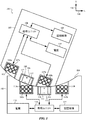
図1は、接続可能な電子デバイスの接続及び整列のためのシステム100を例示する正面等角図である。システムは、第1の電子デバイス101及び第2の電子デバイス102を含み得る。図1は、第1の電子デバイス101を特定形状のハウジングを有するコードレス電子デバイスとして例示し、第2の電子デバイス102をコードレス電子デバイス用のドックとして例示するが、それが単なる例であることが理解される。各種の実施では、第1の電子デバイス101又は第2の電子デバイス102のいずれかは、ラップトップコンピュータ、タブレットコンピュータ、モバイルコンピューティングデバイス、スマートフォン、携帯電話、デジタルメディアプレーヤ、充電及び/又は1つ以上の外部部品への電子デバイスの接続を目的として別の電子デバイスに接続するドック、及び/又はそのような任意の他の電子デバイスなどの、任意の種類の電子デバイスであり得る。
FIG. 1 is a front isometric view illustrating a
例示されるように、第1の電子デバイス101は、第2の電子デバイス102の第2の接続面104に接触するように作用可能である第1の接続面103を含む。幾つかの場合、第1の接続面103及び第2の接続面104は、第1の電子デバイス101と第2の電子デバイス102との間の摺動境界面を形成する。よって、第1及び第2の電子デバイスは、1つ以上の方向で互いに対して配置可能であり得る。
As illustrated, the first
図2は、図1のシステム100の、図1の断面A−Aに沿う正面断面図であり、整列位置にある接続可能な第1及び第2の電子デバイス101及び102を例示する。図3は、図2のシステムを例示し、可能な1つの接触位置にある接続可能な第1及び第2の電子デバイス101及び102を示す。第1及び第2の接続面103及び104は、任意の数の異なる箇所で接触し得る。よって、任意の数の異なる接触位置が可能であり得、図3はその例である。しかし、接続可能な第1及び第2の電子デバイス101及び102は、図2に例示される単一の整列位置を有し得、そこでは、第1の磁気要素105が第2の磁気要素111と接続し、送信部品113a及び113b(単一コイルの複数の断面部分)が受信部品107a及び107b(単一コイルの複数の断面部分)と整列する。
FIG. 2 is a front cross-sectional view of
図2に例示されるように、第1の電子デバイス101は、1つ以上の第1の磁気要素105(永久磁石であり得、シールド要素106を含み得る)、受信部品107a及び107b(シールド要素140a及び140bをそれぞれ含む、単一コイルの複数の断面部分)、処理ユニット108、1つ以上の非一時的な記憶媒体109(非限定的に、磁気記憶媒体、光記憶媒体、光磁気記憶媒体、リードオンリーメモリ、ランダムアクセスメモリ、消去可能プログラマブルメモリ、フラッシュメモリその他の形態をとり得る)、及び/又は1つ以上の電源110(1つ以上のバッテリなど)を含み得る。処理ユニット108は、受信部品を利用する1つ以上の受信動作、通信動作、計算動作、記憶動作、入力/出力動作、時間動作、充電動作その他などの、第1の電子デバイスの1つ以上の動作を実施するために、非一時的な記憶媒体109に記憶された1つ以上の命令を実行し得る。
As illustrated in FIG. 2, the first
同様に、第2の電子デバイス102は、1つ以上の第2の磁気要素111(永久磁石であり得、シールド要素112を含み得る)、送信部品113a及び113b(シールド要素141a及び141bをそれぞれ含む、単一コイルの複数の断面部分)、処理ユニット114、1つ以上の非一時的な記憶媒体115、及び/又は1つ以上の電源116(1つ以上の交流電源若しくは直流電源など)を含み得る。処理ユニット114は、送信部品を利用する1つ以上の送信動作、計算動作、記憶動作その他などの、第1の電子デバイスの1つ以上の動作を実施するために、非一時的な記憶媒体115に記憶された1つ以上の命令を実行し得る。
Similarly, the second
第1及び第2の電子デバイス101及び102が、(図3に示されるような)可能な接触位置のうちの1つに置かれると、第1及び第2の磁気要素105及び111は、第1及び第2の磁気要素の整列に応じて、横方向及び/又は横断方向磁力を及ぼす磁界を発生させ得る。幾つかの場合、横方向199の磁力は、第1及び第2の接続面103及び104の間の境界面と概ね整合する。第1及び第2の磁気要素105及び111の間の横方向199の磁力が電子デバイスを整列位置(図2に示される)に動かし得、そこでは、第1及び第2の磁気要素間の横断方向198の磁力が、2つのデバイスをセンタリング又は整列させるとともに、2つのデバイスの横断方向の接続解除に抵抗し得る。このような動きは、並進と回転の両方であり得(ただし両方である必要はない)、それは、第1及び第2の電子デバイスが未だ回転整列していない場合に、磁気要素の極同士が、第1の電子デバイスを整列位置に回転させるように作用し得るからである。図2及び図3が左右横方向の動きを概して例示するが、それが例であり、横方向の動きは、第1及び第2の接続面103及び104の間の境界面がその動きを許容する限り、2つのデバイスを一次元のみならず二次元で整列させ得る、各種の任意の方向であり得ることが理解される。デバイスのうちの1つ以上は、第1及び第2の接続面103及び104の間の摩擦係数(静的及び/又は動的摩擦係数など)により表現されるような摩擦力を上回るように横方向磁力を生じさせる、各種の特徴のうちの1つ以上を含み得る。
When the first and second
幾つかの実施では、第1及び第2の接続面103及び104のうちの1つ以上は、結晶性材料、摩擦低減被覆又は処理を有する材料、研磨面その他などの低摩擦材料で形成され得る。表面のうちの1つ以上を低摩擦材料から形成することによって、2つの表面間の摩擦係数を上回って、第1及び第2の電子デバイス101及び102を接触位置から整列位置に動かすために必要とされる、横方向磁力が小さくなる。横方向磁力が摩擦係数を上回らない場合、2つの表面間の摩擦によって、2つの位置間の移行が妨げられ、及び/又は、そのような移行がより困難となり得る。
In some implementations, one or more of the first and second connection surfaces 103 and 104 may be formed of a low friction material such as a crystalline material, a material having a friction reducing coating or treatment, a polished surface, or the like. . Required to move the first and second
各種の実施では、第1及び第2の接続面103及び104は、第1及び第2の電子デバイス101及び102が接触位置と整列位置との間を移行するときに、2つの表面間の摩擦係数を最小化するように対応して成形され得る。例えば、図2に示されるように、第1の接続面103は凸状に湾曲し得、第2の接続面104は、第1の接続面の湾曲に対応するように凹状に湾曲し得る。ハウジングのこれらの部分をこのように湾曲させることによって、デバイスの整列が重力により支援され得る。
In various implementations, the first and second connection surfaces 103 and 104 may cause friction between the two surfaces when the first and second
つまり、第1及び接続面103及び104の対応する湾曲は、表面間の摩擦力が十分に弱い場合に、第2の接続に対して第1の接続面が重力により移動されるように形成され得る。よって、重力によって、横方向199の磁力が接続面を整列位置に動かすことが支援され得る。対応する湾曲は、1つ又は複数の表面が動く間の第1及び第2の接続面103及び104の間の摩擦力を小さくするように、被覆され、機械加工され、研磨され、又は他の方法で処理され得る。図3に見ることができるように、第1及び第2の接続面の対応する湾曲は、2つのデバイスを整列位置(図2に示される)に移行させることを重力に支援させ得、第1の電子デバイス101が、第2の接続面104の斜面の高い位置から最も低い位置(すなわち整列位置)に摺動し得る。
That is, the corresponding curvatures of the first and connection surfaces 103 and 104 are formed such that the first connection surface is moved by gravity relative to the second connection when the frictional force between the surfaces is sufficiently weak. obtain. Thus, gravity can help the lateral 199 magnetic force move the connecting surface to the aligned position. The corresponding curvature is coated, machined, polished, or other so as to reduce the frictional force between the first and second connection surfaces 103 and 104 while the one or more surfaces move. Can be processed in a manner. As can be seen in FIG. 3, the corresponding curvatures of the first and second connecting surfaces may allow gravity to assist in moving the two devices to the aligned position (shown in FIG. 2), The
図4は、図2の凹状に湾曲した第2の接続面104が、凸状に湾曲した第1の接続面103にどのように対応し得るかを更に例示する、図2のシステムの、断面B−Bに沿う側断面図である。
4 is a cross-sectional view of the system of FIG. 2, further illustrating how the concavely curved
図3及び図4は、対応する湾曲の特定の例を例示するが、それが例であり、他の対応する表面構成が可能であり企図されることが理解される。例えば、各種の実施では、第2の接続面104は凸状に湾曲し得、第1の接続面103は凹状に湾曲し得る。
3 and 4 illustrate a specific example of the corresponding curvature, it is understood that it is an example and that other corresponding surface configurations are possible and contemplated. For example, in various implementations, the
幾つかの実施では、第1及び第2の磁気要素105及び111の間の横断方向198の磁力は、接触位置と整列位置との間で増加し得る。第1及び第2の接続面103及び104が接触位置では急に引き合わないほど十分に横断方向磁力が弱くされ得るので、そのことは、接続面同士を接触させるときに、知覚できる「スナップ効果」をユーザーが感じることを防ぎ得る。更に、横断方向磁力が各種の接触位置では弱く、整列位置では強くなり得る(接触位置のうちの1つ以上と比較して増加する)ので、磁気要素は、第1及び第2のデバイス101及び102が接触位置から整列位置に移行するときに、第1及び第2の接続面間の摩擦係数を増加させずに、第1及び第2のデバイス101及び102を整列位置で接続するために利用され得る。
In some implementations, the transverse 198 magnetic force between the first and second
例えば、図7Aに例示されるように、磁気要素105及び111のうちの1つ以上は、デバイスが整列位置にないときに、それぞれの接続面から付勢されて離れるように(ばねマウント131及び133にそれぞれ接続されたばね132及び/又は134を介してなど)移動可能に取り付けられ得る。図7Bに例示されるように、デバイスが整列位置に移行するときに、横断方向198の磁力によって、磁気要素はそれぞれの接続面に向けて動かされ(ばね132及び/又は134を伸ばし)得る。
For example, as illustrated in FIG. 7A, one or more of the
更に、図2を再び参照すると、各種の実施では、第1及び第2の磁気要素105及び111は、それぞれシールド要素106及び112を含み得る。各磁気要素は、前面がそれぞれの接続面に面する(面するように示される)ように、複数の側面により接合される前面及び後面を有し得る。それぞれのシールド要素は、後面及び2つの側面を少なくとも部分的に覆い得る。隙間117又は118が、それぞれのシールド要素と複数の側面との間に存在し(それらによって画定され)、それらをオフセットし得る。
Further, referring again to FIG. 2, in various implementations, the first and second
シールド要素106又は112は、軟磁性材料、強磁性材料、及び/又は、鉄コバルトなど容易に帯磁する可能性を示す任意の他の材料で形成され得、磁気要素の磁界を接続面の方向に向け得る。このような方向の磁界は、他の方法で可能になるよりも小さな磁気要素の使用を可能にし得、磁気要素間の横方向199の磁力に悪影響を及ぼさずに、磁気要素間の横断方向198の磁力が、第1及び第2のデバイス101及び102が整列位置にあるときに強くなり、デバイスが接触位置にあるときに弱くなることを可能にし得る。
The
図5Aは、図2の第1の電子デバイス101及びシールド要素106から取り外された、第1の磁気要素105の磁界120A(サンプル力線を含む)を例示する。比較として、図5Bは、図2の第1の電子デバイス101から取り外された、シールド要素106を含む第1の磁気要素105の磁界120A(再びサンプル力線を含む)を例示する。図5Aと図5Bの比較により分かるように、シールド要素106を含むことによって、磁界120Aが第1の接続面103に向けられ得る。
FIG. 5A illustrates the
図5A及び図5Bが磁界120Aの方向を1つのサンプル方向に循環するものとして例示するが、それが例であることが理解される。他の実施形態では、磁界120Aは、本開示の範囲から逸脱せずに反転され得る。
Although FIGS. 5A and 5B illustrate the direction of the
図2に戻ると、幾つかの実施では、第1の電子デバイス101は、第2の電子デバイス102の1つ以上の送信部品113a及び113bから受信するように動作可能な1つ以上の受信部品107a及び107bを含み得る。このような場合、2つのデバイスの接続及び整列は、受信及び送信部品を整列させることを少なくとも目的とし得る。
Returning to FIG. 2, in some implementations, the first
例えば、送信部品113a及び113b(シールド要素141a及び141bをそれぞれ含む、単一コイルの複数の断面部分)は、誘導電力送信部品であり得、受信部品107a及び107b(シールド要素140a及び140bをそれぞれ含む、単一コイルの複数の断面部分)は、誘導電力受信部品であり得る。したがって、第1及び第2の電子デバイス101及び102の接続及び整列は、誘導電力受信部品107a及び107b並びに誘導電力送信部品113a及び113bを整列させることを少なくとも目的とし得る。
For example,
更に、受信部品107a及び107bが第1の電子デバイス101の上面に概ね平行であるものとして示され、送信部品113a及び113bが、第1及び第2の接続面103及び104と同一面に整列されないように、第2の電子デバイス102の下面に概ね平行であるものとして示されるが、それが例であることが理解される。他の実施では、本開示の範囲から逸脱せずに、受信部品107a及び107bは、湾曲し、第1の接続面103と同一面にあり得、及び/又は、送信部品113a及び113bは、湾曲し、第2の接続面104と同一面にあり得る。このような実施では、受信部品107a及び107b並びに送信部品113a及び113bは、第1の電子デバイス101の上面及び/又は第2の電子デバイス102の下面に対して傾斜し得る。
Further, the receiving
幾つかの場合、第2の電子デバイス102は、第1の電子デバイス101のためのドックとして動作し得る。例えば、上で議論されたように、第1及び第2の電子デバイス101及び102は、誘導電力の送信部品113a及び113b並びに受信部品107a及び107bを含み、第1及び第2の電子デバイス101及び102は、誘導電力送信システムに関与し得、そこでは、第2の電子デバイス102が、第1の電子デバイス101に電力を誘導送信することにより、第1の電子デバイス101のための充電ドックとして機能し、その電力を第1の電子デバイス101が電源110に貯蔵する。
In some cases, the second
図6は、接続可能な電子デバイスの接続及び整列のための方法600を例示する方法図である。この方法は、例えば図1のシステムにより実施され得る。
FIG. 6 is a method diagram illustrating a
フローは、ブロック601にて始まり得、そこでは、第1の電子デバイスの第1の接続面が、接触位置にある第2の電子デバイスの第2の接続面と接触される。フローは、次いでブロック602に進み得る。
The flow may begin at
ブロック602にて、第1及び第2の電子デバイスは、第1及び第2の電子デバイスの第1及び第2の磁気要素間の横方向磁力をそれぞれ利用して、接触位置から整列位置に動かされる。このような動きは、横方向と回転の両方であり得、磁気要素の極同士は、場合によって電子デバイスのうちの1つ以上を整列位置に回転させるように作用する。横方向磁力は、第1及び第2の接続面の摩擦係数を上回り得る。フローは、次いでブロック603に進み得、そこでは、第1及び第2の電子デバイスは、第1及び第2の磁気要素間の横断方向磁力を利用して、整列位置で接続される。
At
方法600は特定の順序で実施される特定の動作を含むとして例示及び上述されるが、それが例であることが理解される。各種の実施では、同じ、同様及び/又は異なる動作の各種の構成が、本開示の範囲から逸脱せずに実施され得る。例えば、ブロック602及び603は、線形順序で実施されるとして例示及び記述される。しかし、各種の実施では、これらの動作は、並列に又は実質的に並列に実施され得る。
Although
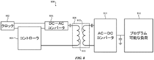
次に図8を参照すると、図2のシステム100の送信部品113a及び113b並びに受信部品107a及び107bとともに利用され得る、周波数制御される例示的な誘導充電システム800の簡略化されたブロック図が示される。誘導充電システムは、コントローラ804及び直流コンバータ806に動作的に接続されたクロック回路802を含む。クロック回路802は、誘導充電システム800のためのタイミング信号を発生させることができる。
Referring now to FIG. 8, a simplified block diagram of an exemplary frequency controlled
コントローラ804は、直流コンバータ806の状態を制御することができる。一実施形態では、クロック回路802は、直流コンバータ806内のスイッチを1サイクルベースで作動及び停止させるためにコントローラ804により使用される周期信号を発生させる。誘導充電システム800では、任意の適当な直流コンバータ806を使用することができる。例えば、一実施形態では、直流コンバータとしてHブリッジが使用され得る。Hブリッジは、当該分野で知られているので、本明細書ではHブリッジの動作の概要のみが記述される。
The controller 804 can control the state of the
コントローラ804は、4つのスイッチS1、S2、S3、S4(例示されない)の開閉を制御する。スイッチS1及びS4が所与の期間にわたって閉じられ、スイッチS2及びS3が開かれると、正極から負荷を通って負極に電流が流れ得る。同様に、スイッチS2及びS3が所与の別の期間にわたって閉じられる一方、スイッチS1及びS4が開かれると、負極から正極に電流が流れ得る。スイッチのこの開閉によって、同じ負荷を通る電流の方向を繰返し反転させることにより時間変動する電流が作り出される。 The controller 804 controls opening and closing of four switches S1, S2, S3, and S4 (not illustrated). When switches S1 and S4 are closed for a given period and switches S2 and S3 are opened, current can flow from the positive electrode through the load to the negative electrode. Similarly, when switches S2 and S3 are closed for a given different period of time, when switches S1 and S4 are opened, current can flow from the negative electrode to the positive electrode. This opening and closing of the switch creates a time-varying current by repeatedly reversing the direction of the current through the same load.
代替的な実施形態では、Hブリッジが必要とされない場合もある。例えば、直流コンバータ806からの電流の流れを単一のスイッチが制御し得る。このようにして、直流コンバータ806は、矩形波発生器として機能し得る。
In alternative embodiments, an H-bridge may not be required. For example, a single switch can control the flow of current from the
直流コンバータ806により作り出された時変信号又は矩形波信号は、変圧器808に入力され得る。典型的に、上で参照したテザー充電システムに使用されるような変圧器は、二次コイルに結合された一次コイルを含み、各コイルが共通コアの周りに巻き付けられる。しかし、本明細書に記述されるような誘導充電システムは、空隙により分離された一次及び二次コイルと、各コイルを収容する各ハウジングと、を含む。よって、例示されるように、変圧器808は、必ずしも物理的な要素でなくてもよく、代わりに、一次コイル810(図2のシステム100の送信部品113a及び113bであり得る)及び二次コイル812(図2のシステム100の受信部品107a及び107bであり得る)などの、誘導的に近接する2つの電磁コイル間の関係及びインタフェースを意味し得る。
A time varying signal or a square wave signal produced by the
送信器、及び誘導電力送信システムの二次コイル812との送信器の相互作用の簡略化された説明を前述した。送信器は、二次コイル812に電圧を誘導するために、時間変動する電圧を一次コイル810に提供するように構成され得る。交流及び矩形波の両方が例として指摘されたが、他の波形が企図されることが理解され得る。このような場合、コントローラ804は、直流コンバータ806の多数の状態を制御し得る。例えば、コントローラ804は、電圧、電流、デューティサイクル、波形、周波数、又はそれらの任意の組み合わせを制御し得る。
A simplified description of the transmitter and the interaction of the transmitter with the
コントローラ804は、電力送信回路の動作効率を高めるために、一次コイル810に適用される波形の各種の特性を周期的に修正し得る。例えば、幾つかの場合、コントローラ804は、二次コイル812が一次コイル810に誘導的に近接していないと判定した場合に、一次コイル810への全ての電力を停止させ得る。この判定は、任意の数の適当な方法で達成され得る。例えば、コントローラ804は、一次コイル810上の誘導負荷を検出するように構成され得る。誘導負荷が一定の選択閾値を下回る場合、コントローラ804は、二次コイル812が一次コイル810に誘導的に近接していないと結論付け得る。このような場合、コントローラ804は、一次コイル810への全ての電力を停止させ得る。
The controller 804 can periodically modify various characteristics of the waveform applied to the
他の場合、一実施形態では、コントローラ804は、変圧器808の共振周波数に又はその近くにデューティサイクルを設定し得る。別の例では、デューティサイクルの作動状態を規定する波形(すなわちハイ)の周期は、変圧器808の共振周波数で又はその近くで選択され得る。このような選択によって一次コイル810と二次コイル812との間の電力伝送効率が高まり得ることが理解され得る。
In other cases, in one embodiment, the controller 804 may set the duty cycle at or near the resonant frequency of the
代替的な例では、コントローラ804は、誘導負荷のスパイクが検知された場合に一次コイル810への全ての電力を停止させ得る。例えば、一定の選択閾値を上回る特定のレートで誘導負荷がスパイクを示した場合、コントローラ804は、一次コイル810に誘導的に近接する中間物体が置かれていると結論付け得る。このような場合、コントローラ804は、一次コイル810への全ての電力を停止させ得る。
In an alternative example, the controller 804 may turn off all power to the
また更なる例では、コントローラ804は、一次コイル810に適用される波形の他の特性を修正し得る。例えば、受信器回路が追加の電力を必要とする場合、コントローラ804は、一次コイル810に適用される波形のデューティサイクルを増加させ得る。関連する例では、受信器回路がより少ない電力を必要とする場合、コントローラ804は、一次コイル810に適用される波形のデューティサイクルを減少させ得る。これらの例のそれぞれでは、一次コイル810に適用される時間平均電力が修正され得る。
In yet a further example, the controller 804 may modify other characteristics of the waveform applied to the
また別の例では、コントローラ804は、一次コイル810に適用される波形の大きさを修正するように構成され得る。このような例では、受信器回路が追加の電力を必要とする場合、コントローラ804は、一次コイル810に適用される波形の最大電圧を増幅させ得る。関連する場合では、波形の最大電圧は、受信器回路がより少ない電力を必要とする場合に減少され得る。
In yet another example, the controller 804 can be configured to modify the magnitude of the waveform applied to the
図8を参照すると、上記したように、誘導電力送信システムの送信器部分は、一次コイル810と二次コイル812との間の誘導結合を通じて受信器内の二次コイル812内に電圧を誘導するために、一次コイル810に時変信号を提供するように構成され得る。このようにして、一次コイル810の時変信号により変化する磁界の形成によって、一次コイル810から二次コイル812に電力が伝送され得る。
Referring to FIG. 8, as described above, the transmitter portion of the inductive power transmission system induces a voltage in the
二次コイル812に作り出された時変信号は、時変信号をDC信号に変換する直流コンバータ814により受信され得る。誘導充電システム800では、任意の適当な直流コンバータ814を使用することができる。例えば、一実施形態では、直流コンバータとして整流器が使用され得る。DC信号は、次いでプログラム可能な負荷816により受信され得る。
The time-varying signal created in the
幾つかの実施形態では、受信器の直流コンバータ814はハーフブリッジであり得る。このような例では、二次コイル812は、より多くの巻線を有し得る。例えば、幾つかの実施形態では、二次コイルは、2倍の巻線を有し得る。このようにして、理解され得るように、二次コイル812を横切る誘導電圧は、ハーフブリッジ整流器により効果的に半減され得る。幾つかの場合、この構成は、実質的により少ない電子部品を必要とし得る。例えば、ハーフブリッジ整流器は、全波ブリッジ整流器の半分のトランジスタを必要とし得る。より少ない電子部品の結果として、抵抗損失が大幅に小さくなり得る。
In some embodiments, the
他の幾つかの実施形態では、受信器は、送信器内に存在する磁化インダクタンスを調整除去するための回路も含み得る。当該分野で知られているように、磁化インダクタンスは、不完全に結合されたコイルにより形成された変圧器内で損失を生じさせ得る。他の漏洩インダクタンスのうち、この磁化インダクタンスによって、送信器の効率が大幅に低下し得る。磁化インダクタンスが一次及び二次コイル間の結合に依存し得るため、送信器自体の内部で必ずしも完全には補償され得ないことが更に理解され得る。これにより、本明細書で議論される幾つかの実施形態では、受信器内に調整回路が含まれ得る。例えば、幾つかの実施形態では、プログラム可能な負荷816と並列にコンデンサが配置され得る。
In some other embodiments, the receiver may also include a circuit for trimming out the magnetizing inductance present in the transmitter. As is known in the art, magnetizing inductance can cause losses in transformers formed by imperfectly coupled coils. Among other leakage inductances, this magnetizing inductance can greatly reduce the efficiency of the transmitter. It can be further understood that the magnetizing inductance can depend on the coupling between the primary and secondary coils and therefore cannot always be fully compensated within the transmitter itself. Thus, in some embodiments discussed herein, a conditioning circuit may be included in the receiver. For example, in some embodiments, a capacitor may be placed in parallel with the
また更なる例では、上で参照したサンプル修正形態の組み合わせがコントローラにより成され得る。例えば、コントローラ804は、デューティサイクルを減少させることに加えて電圧を2倍にし得る。別の例では、コントローラは、デューティサイクルを時間とともに減少させながら電圧を時間とともに増加させ得る。本明細書では任意の数の適当な組み合わせが企図されることが理解され得る。 In yet a further example, a combination of the sample modifications referenced above can be made by the controller. For example, the controller 804 may double the voltage in addition to reducing the duty cycle. In another example, the controller may increase the voltage over time while decreasing the duty cycle over time. It can be appreciated that any number of suitable combinations are contemplated herein.
他の実施形態は、複数の一次コイル810を含み得る。例えば、2つの一次コイルが存在する場合、それぞれが単独で又は同時に作動されたり使用されたりし得る。このような実施形態では、個々のコイルは、それぞれコントローラ804に結合され得る。更なる例では、幾つかの個々の一次コイル810のうちの1つが選択的にショートされ得る。例えば、スイッチがオフのときに電流が誘導子を通って流れ得るように、コイルと並列にスイッチが配置され得る。一方、スイッチがオンのときには、電流はコイルを通じて流れない。スイッチは、手動、ソリッドステート、又はリレーベースのスイッチのうちの任意の適当なタイプであり得る。このようにして、幾つかのコイルのそれぞれを通る電流の増加量は、選択的に制御され得る。例えば、誘導負荷が高い状況では、スイッチは、一次コイル810を伴う回路内にコイルを含むように切断され得る。
Other embodiments may include a plurality of
図9〜図11は、本明細書に開示される磁気的な接続及び整列技術の各種の実施形態が利用され得る、サンプル電子デバイス901〜1101の等角図を例示する。例示されるように、図9はスマートフォン901を例示し、図10はタブレットコンピュータ1001を例示し、図11は、ここでは腕時計として示されるウェアラブルデバイス1101を例示する。しかし、これらが例であり、本明細書に開示される磁気的な接続及び整列技術の実施形態が、本開示の範囲から逸脱せずに、広範な異なる電子デバイスで利用され得ることが理解される。
9-11 illustrate isometric views of sample electronic devices 901-1101 in which various embodiments of the magnetic connection and alignment techniques disclosed herein can be utilized. As illustrated, FIG. 9 illustrates a
図1〜図8は、部品の各種の構成(受信部品107a及び107b、送信部品113a及び113b、並びに磁気要素105及び111など)を例示するが、それらが例であることが理解される。各種の実施では、本開示の範囲から逸脱せずに各種の他の構成が可能である。
1-8 illustrate various configurations of components (such as receiving
例えば、図12は、図11のウェアラブルデバイス1101の、図11の断面C−Cに沿う概略側断面図であり、受信部品1107a及び1107b、第1の磁気要素1105、第1の接続面1103、シールド要素1140a及び1140b、並びにシールド要素1106の、別のサンプル構成を例示する。しかし、この構成も例であり、本開示の範囲から逸脱せずに、また他の構成が可能であることが理解される。加えて、ウェアラブルデバイス1101は、図12の側断面図では明瞭性のために省略されている他の部品を含み得る。ウェアラブルデバイスは、そのハウジング内に、任意の又は全ての又は複数の、入力機構、プロセッサ、メモリ、ディスプレイ、モータなどの出力要素、センサその他を含み得る。
For example, FIG. 12 is a schematic side cross-sectional view of the
上述し、添付図面に例示されるように、本開示は、接続可能な電子デバイスの接続及び整列のためのシステム及び方法を開示する。接続可能な第1及び第2の電子デバイスが、それぞれ接続面及び磁気要素を含み得る。2つのデバイスは、異なる多数の可能な接触位置のうちの1つに置かれ得、そこでは、接続面同士は接触し、2つの表面間の摩擦係数を上回る磁気要素間の横方向磁力によって、2つのデバイスが整列位置と動かされ得る。デバイスが整列位置にあるときに、磁気要素の横断方向磁力は、2つのデバイスを接続し得る。任意選択的に、デバイスが整列位置にあるときに、一方のデバイスの、他方のデバイスからの誘導充電が起き得る。 As described above and illustrated in the accompanying drawings, the present disclosure discloses systems and methods for connecting and aligning connectable electronic devices. The connectable first and second electronic devices may each include a connection surface and a magnetic element. The two devices can be placed in one of a number of different possible contact positions, where the connecting surfaces are in contact and the transverse magnetic force between the magnetic elements exceeds the coefficient of friction between the two surfaces, Two devices can be moved to the aligned position. When the device is in the aligned position, the transverse magnetic force of the magnetic element can connect the two devices. Optionally, inductive charging of one device from the other device can occur when the device is in the aligned position.
本開示では、開示された方法は、命令又は動作のセットを利用し得る。開示された方法におけるステップの具体的な順序又は階層は、サンプルアプローチの例であることが理解される。他の実施形態では、方法におけるステップの具体的な順序又は階層を、開示された主題の範囲内にて再編成することができる。付随する方法の請求項は、各種のステップの要素をサンプル順序で提示し、提示される具体的な順序又は階層に必ずしも限定されることを意図しない。 In the present disclosure, the disclosed method may utilize a set of instructions or actions. It is understood that the specific order or hierarchy of steps in the disclosed methods is an example of a sample approach. In other embodiments, the specific order or hierarchy of steps in the methods can be rearranged within the scope of the disclosed subject matter. The accompanying method claims present elements of the various steps in a sample order, and are not necessarily intended to be limited to the specific order or hierarchy presented.
本開示及びその付随する利点の多くは、前述の説明により理解されるであろうことが信じられ、部品の形態、構造、及び配列における各種の変更が、開示された主題から逸脱することなく、又はその有形の利点の全てを損なうことなく、行われ得ることが明らかとなるであろう。記述された形態は単に説明的なものであり、そのような変更を包含し、含むことは、以下の請求項の意図するところである。 It is believed that many of the present disclosure and its attendant advantages will be understood from the foregoing description, and various changes in the form, structure, and arrangement of parts can be made without departing from the disclosed subject matter. Or it will be clear that this can be done without compromising all of its tangible advantages. The form described is merely illustrative and includes and includes such modifications as are the intention of the following claims.
各種の実施形態を参照して、本開示を記述してきたが、これらの実施形態は例示的なものであり、本開示の範囲は、それらに限定されるものではないことが理解されるであろう。多くの変形、修正、追加、及び改善が可能である。より一般的に、本開示による実施形態は、コンテキスト又は特定の実施形態にて記述されてきた。本開示の各種の実施形態では、機能性は、ブロック内で異なるように分離若しくは組み合わせられ得、又は異なる専門用語で記述され得る。これらの変形、修正、追加、及び改善、並びに他の変形、修正、追加、及び改善は、以下の請求項で定義されるような、本開示の範囲内に包含され得る。 Although the present disclosure has been described with reference to various embodiments, it is understood that these embodiments are illustrative and that the scope of the disclosure is not limited thereto. Let's go. Many variations, modifications, additions and improvements are possible. More generally, embodiments according to the present disclosure have been described in contexts or specific embodiments. In various embodiments of the present disclosure, functionality may be separated or combined differently within a block, or may be described in different terminology. These variations, modifications, additions and improvements, as well as other variations, modifications, additions and improvements, may be encompassed within the scope of the disclosure as defined in the following claims.
Claims (23)
前記接続面に隣接して前記ハウジング内に配置された磁気要素と、を備え、
前記磁気要素が、整列位置を達成するべく、前記ハウジング及び外部面のうちの一方を他方に対して移動させることにより、前記ハウジングを隣接する外部面と整列させるように構成され、
前記磁気要素が、前記ハウジング及び外部面が前記整列位置にあるときに、前記外部面からの前記ハウジングの接続解除に抵抗するように更に構成される、電子デバイス。 A housing defining a connection surface;
A magnetic element disposed in the housing adjacent to the connection surface,
The magnetic element is configured to align the housing with an adjacent outer surface by moving one of the housing and the outer surface relative to the other to achieve an aligned position;
An electronic device, wherein the magnetic element is further configured to resist disconnection of the housing from the outer surface when the housing and outer surface are in the aligned position.
前記磁界が、前記ハウジング及び外部面のうちの一方を他方に対して移動させるように横方向磁力を及ぼす、請求項1に記載の電子デバイス。 The magnetic element generates a magnetic field;
The electronic device of claim 1, wherein the magnetic field exerts a transverse magnetic force to move one of the housing and an outer surface relative to the other.
前記横断方向磁力が、前記接触位置よりも前記整列位置で大きい、請求項4に記載の電子デバイス。 The magnetic field exerts a transverse magnetic force to resist disconnection of the housing from the outer surface;
The electronic device of claim 4, wherein the transverse magnetic force is greater at the aligned position than at the contact position.
第1の電子デバイスであって、
第1のハウジングと、
前記第1のハウジング内に配置された第1の磁気要素と、を備える第1の電子デバイスと、
第2の電子デバイスであって、
第2のハウジングと、
前記第2のハウジング内に配置された第2の磁気要素と、を備える第2の電子デバイスと、を備え、
前記第1及び第2の磁気要素が、前記第1及び第2の電子デバイスを互いに対して初期位置から整列位置に移動させるように作用する磁力を発生させ、
前記第1のハウジング及び第2のハウジングが、前記初期位置と前記整列位置の両方で互いに接触する、システム。 A system for magnetic connection and alignment, the system comprising:
A first electronic device comprising:
A first housing;
A first electronic device comprising: a first magnetic element disposed within the first housing;
A second electronic device comprising:
A second housing;
A second electronic device comprising: a second magnetic element disposed within the second housing;
The first and second magnetic elements generate a magnetic force that acts to move the first and second electronic devices relative to each other from an initial position to an aligned position;
The system, wherein the first housing and the second housing contact each other in both the initial position and the aligned position.
前記第1及び第2の電子デバイスが前記初期位置から前記整列位置に移動するときに、前記横断方向磁力が、前記第1の磁気要素を前記第1の接続面に向けて引っ張る、請求項6に記載のシステム。 The first connection of the first housing when the first magnetic element is movably mounted in the first housing and the first and second electronic devices are not in the aligned position. Energized away from the surface,
The transverse magnetic force pulls the first magnetic element toward the first connection surface as the first and second electronic devices move from the initial position to the aligned position. The system described in.
前記第1のハウジングの第1の接続面に面し、複数の側面により後面に接合される、前面と、
前記後面及び前記複数の側面を少なくとも部分的に覆うシールド要素と、を備える、請求項6に記載のシステム。 The first magnetic element comprises:
A front surface facing the first connection surface of the first housing and joined to the rear surface by a plurality of side surfaces;
And a shielding element that at least partially covers the rear surface and the plurality of side surfaces.
前記第2のデバイスの前記第2の接続面に面し、複数の側面により後面に接合される、前面と、
前記後面及び前記複数の側面を少なくとも部分的に覆うシールド要素と、を備える、請求項6に記載のシステム。 The second magnetic element comprises:
A front surface facing the second connection surface of the second device and joined to the rear surface by a plurality of side surfaces;
And a shielding element that at least partially covers the rear surface and the plurality of side surfaces.
第1の電子デバイスを第2の電子デバイスに対して接触位置から整列位置に磁気的に移動させることと、
前記第1の電子デバイスの第1の磁気要素と、前記第2の電子デバイスの第2の磁気要素との間の磁力を利用して、前記第1の電子デバイス及び前記第2の電子デバイスを前記整列位置に保持することと、を含む方法。 A method for magnetic connection and alignment of connectable electronic devices comprising:
Magnetically moving the first electronic device from the contact position to the aligned position relative to the second electronic device;
Using the magnetic force between the first magnetic element of the first electronic device and the second magnetic element of the second electronic device, the first electronic device and the second electronic device are Holding in the aligned position.
Applications Claiming Priority (3)
| Application Number | Priority Date | Filing Date | Title |
|---|---|---|---|
| US201461969343P | 2014-03-24 | 2014-03-24 | |
| US61/969,343 | 2014-03-24 | ||
| PCT/US2015/022195 WO2015148473A1 (en) | 2014-03-24 | 2015-03-24 | Magnetic connection and alignment of connectible devices |
Publications (2)
| Publication Number | Publication Date |
|---|---|
| JP2017511677A true JP2017511677A (en) | 2017-04-20 |
| JP6335322B2 JP6335322B2 (en) | 2018-05-30 |
Family
ID=52823838
Family Applications (1)
| Application Number | Title | Priority Date | Filing Date |
|---|---|---|---|
| JP2016554719A Active JP6335322B2 (en) | 2014-03-24 | 2015-03-24 | Magnetic connection and alignment of connectable devices |
Country Status (7)
| Country | Link |
|---|---|
| US (1) | US9627130B2 (en) |
| EP (2) | EP3379549B1 (en) |
| JP (1) | JP6335322B2 (en) |
| KR (1) | KR101920545B1 (en) |
| CN (1) | CN106133850B (en) |
| AU (1) | AU2015236282B2 (en) |
| WO (1) | WO2015148473A1 (en) |
Families Citing this family (27)
| Publication number | Priority date | Publication date | Assignee | Title |
|---|---|---|---|---|
| JP6335322B2 (en) | 2014-03-24 | 2018-05-30 | アップル インコーポレイテッド | Magnetic connection and alignment of connectable devices |
| US9852844B2 (en) | 2014-03-24 | 2017-12-26 | Apple Inc. | Magnetic shielding in inductive power transfer |
| US9853507B2 (en) | 2014-05-05 | 2017-12-26 | Apple Inc. | Self-locating inductive coil |
| US9735629B2 (en) | 2014-05-28 | 2017-08-15 | Apple Inc. | Electromagnetic alignment of inductive coils |
| US10181640B2 (en) | 2016-08-11 | 2019-01-15 | Apple Inc. | Electronic device antennas |
| US10367252B2 (en) | 2016-08-11 | 2019-07-30 | Apple Inc. | Broadband antenna |
| US20180123392A1 (en) * | 2016-10-31 | 2018-05-03 | Apple Inc. | Wireless Charging System With Solenoids |
| EP3351138B1 (en) * | 2017-01-20 | 2020-09-09 | The Gillette Company LLC | Personal care product docking system |
| EP3351133B1 (en) * | 2017-01-20 | 2020-09-09 | The Gillette Company LLC | Personal care product stand |
| USD831375S1 (en) | 2017-01-20 | 2018-10-23 | The Gillette Company Llc | Shaving razor stand |
| EP3477811A1 (en) | 2017-10-31 | 2019-05-01 | HMD global Oy | Wireless charging feature for wireless device and wireless charging method having a backoff feature |
| CN108832411A (en) * | 2018-06-16 | 2018-11-16 | 北京设集约科技有限公司 | A kind of electromagnetism lock system and its control method for charging interface |
| CN108832412A (en) * | 2018-06-16 | 2018-11-16 | 北京设集约科技有限公司 | A kind of electromagnetic lock and its control method for charging interface |
| CN108832410A (en) * | 2018-06-16 | 2018-11-16 | 北京设集约科技有限公司 | A kind of electromagnetic lock and its control method for charging interface |
| CN108964198A (en) * | 2018-08-07 | 2018-12-07 | Oppo广东移动通信有限公司 | Charging device of electronic appliances, wireless charging management method and electronic device charging system |
| US10671121B2 (en) | 2018-09-14 | 2020-06-02 | Apple Inc. | Magnetic layout in electronic devices and accessory devices for electronic devices |
| KR102638776B1 (en) * | 2019-01-04 | 2024-02-21 | 주식회사 아모센스 | RF Connector |
| MX2021010705A (en) * | 2019-03-07 | 2021-12-10 | Hubbell Inc | Inductive power transfer. |
| KR20200117165A (en) | 2019-04-03 | 2020-10-14 | 주식회사 아모센스 | Flexible Cable Jumper Apparatus and Manufacturing Method For The Same |
| US11710988B2 (en) | 2019-09-27 | 2023-07-25 | Apple Inc. | Magnetic alignment systems with NFC for electronic devices |
| US11722015B2 (en) | 2019-09-27 | 2023-08-08 | Apple Inc. | Wireless charging modules with magnetic alignment components |
| US11675440B2 (en) | 2019-09-30 | 2023-06-13 | Microsoft Technology Licensing, Llc | Solvent free textile coating |
| US11239710B2 (en) * | 2019-09-30 | 2022-02-01 | Microsoft Technology Licensing, Llc | Charging system including orientation control |
| KR20210111032A (en) | 2020-03-02 | 2021-09-10 | 삼성전자주식회사 | Electronic device display state of alignment for wireless charging |
| US11867352B2 (en) | 2020-08-05 | 2024-01-09 | Apple Inc. | Adapter for charging and stabilizing cameras |
| US11839279B2 (en) | 2020-09-22 | 2023-12-12 | Apple Inc. | Magnetically attachable wallet |
| US20220376387A1 (en) * | 2021-05-21 | 2022-11-24 | Hewlett-Packard Development Company, L.P. | Movable antenna radiators |
Citations (7)
| Publication number | Priority date | Publication date | Assignee | Title |
|---|---|---|---|---|
| JP2003118671A (en) * | 2001-08-09 | 2003-04-23 | Sumitomo Wiring Syst Ltd | Charging system for power-assisted small vehicle |
| JP2010272628A (en) * | 2009-05-20 | 2010-12-02 | Toshiba Corp | Power supplying apparatus |
| JP2011514796A (en) * | 2008-02-22 | 2011-05-06 | アクセス ビジネス グループ インターナショナル リミテッド ライアビリティ カンパニー | Magnetic positioning for inductive coupling |
| JP2011120432A (en) * | 2009-12-07 | 2011-06-16 | Sanyo Electric Co Ltd | Power transportation system, power receiver, and method of manufacturing the power receiver |
| JP2012199370A (en) * | 2011-03-22 | 2012-10-18 | Hitachi Metals Ltd | Coil component and power supply device using the same, and charger |
| JP2012530481A (en) * | 2009-06-25 | 2012-11-29 | 株式会社村田製作所 | Power transmission system and non-contact charging device |
| WO2013024395A2 (en) * | 2011-08-16 | 2013-02-21 | Koninklijke Philips Electronics N.V. | Receiver electrodes of a capacitive wireless powering system |
Family Cites Families (30)
| Publication number | Priority date | Publication date | Assignee | Title |
|---|---|---|---|---|
| DE69831226T2 (en) | 1997-11-20 | 2006-03-30 | Seiko Epson Corp. | ELECTRONIC DEVICE |
| US7477039B2 (en) * | 2005-05-19 | 2009-01-13 | International Business Machines Corporation | Method and apparatus for charging a portable electrical device |
| US7351066B2 (en) | 2005-09-26 | 2008-04-01 | Apple Computer, Inc. | Electromagnetic connector for electronic device |
| US7952322B2 (en) | 2006-01-31 | 2011-05-31 | Mojo Mobility, Inc. | Inductive power source and charging system |
| US8169185B2 (en) | 2006-01-31 | 2012-05-01 | Mojo Mobility, Inc. | System and method for inductive charging of portable devices |
| US7948208B2 (en) | 2006-06-01 | 2011-05-24 | Mojo Mobility, Inc. | Power source, charging system, and inductive receiver for mobile devices |
| US20110050164A1 (en) | 2008-05-07 | 2011-03-03 | Afshin Partovi | System and methods for inductive charging, and improvements and uses thereof |
| US8497657B2 (en) | 2008-06-27 | 2013-07-30 | Microsoft Corporation | Docking station for electronic device |
| US8401469B2 (en) * | 2008-09-26 | 2013-03-19 | Hewlett-Packard Development Company, L.P. | Shield for use with a computing device that receives an inductive signal transmission |
| CN101841173B (en) | 2009-03-19 | 2013-04-24 | 鸿富锦精密工业(深圳)有限公司 | Charging system |
| US8890470B2 (en) | 2010-06-11 | 2014-11-18 | Mojo Mobility, Inc. | System for wireless power transfer that supports interoperability, and multi-pole magnets for use therewith |
| TW201236299A (en) * | 2010-11-04 | 2012-09-01 | Access Business Group Int Llc | Wireless power system and method with improved alignment |
| US8382486B2 (en) | 2010-12-22 | 2013-02-26 | Research In Motion Limited | Self-orienting electrical connector |
| EP2469663B1 (en) | 2010-12-24 | 2020-06-17 | Phitek Systems Limited | Magnetic connector apparatus |
| US9496732B2 (en) | 2011-01-18 | 2016-11-15 | Mojo Mobility, Inc. | Systems and methods for wireless power transfer |
| US9178369B2 (en) | 2011-01-18 | 2015-11-03 | Mojo Mobility, Inc. | Systems and methods for providing positioning freedom, and support of different voltages, protocols, and power levels in a wireless power system |
| US20130285605A1 (en) | 2011-01-18 | 2013-10-31 | Mojo Mobility, Inc. | Systems and methods for wireless power transfer |
| US10115520B2 (en) | 2011-01-18 | 2018-10-30 | Mojo Mobility, Inc. | Systems and method for wireless power transfer |
| WO2013015540A1 (en) * | 2011-07-26 | 2013-01-31 | Lg Innotek Co., Ltd. | Wireless power transmitter and wireless power receiver |
| JP4900528B1 (en) | 2011-09-08 | 2012-03-21 | パナソニック株式会社 | Non-contact charging module and non-contact charging device using the same |
| WO2013038591A1 (en) * | 2011-09-16 | 2013-03-21 | パナソニック株式会社 | Power-reception device, power-transmission device, and power-transfer device |
| US9722447B2 (en) | 2012-03-21 | 2017-08-01 | Mojo Mobility, Inc. | System and method for charging or powering devices, such as robots, electric vehicles, or other mobile devices or equipment |
| US20130271069A1 (en) | 2012-03-21 | 2013-10-17 | Mojo Mobility, Inc. | Systems and methods for wireless power transfer |
| US9196417B2 (en) * | 2012-05-04 | 2015-11-24 | Det International Holding Limited | Magnetic configuration for high efficiency power processing |
| TWI600248B (en) * | 2012-05-20 | 2017-09-21 | 通路實業集團國際公司 | Wireless power supply system |
| US20140191568A1 (en) | 2013-01-04 | 2014-07-10 | Mojo Mobility, Inc. | System and method for powering or charging multiple receivers wirelessly with a power transmitter |
| US9837846B2 (en) | 2013-04-12 | 2017-12-05 | Mojo Mobility, Inc. | System and method for powering or charging receivers or devices having small surface areas or volumes |
| JP6335322B2 (en) | 2014-03-24 | 2018-05-30 | アップル インコーポレイテッド | Magnetic connection and alignment of connectable devices |
| KR101951531B1 (en) | 2014-03-26 | 2019-02-22 | 애플 인크. | Temperature management for inductive charging systems |
| US9735629B2 (en) | 2014-05-28 | 2017-08-15 | Apple Inc. | Electromagnetic alignment of inductive coils |
-
2015
- 2015-03-24 JP JP2016554719A patent/JP6335322B2/en active Active
- 2015-03-24 US US14/666,556 patent/US9627130B2/en active Active
- 2015-03-24 EP EP18171711.7A patent/EP3379549B1/en active Active
- 2015-03-24 KR KR1020167025043A patent/KR101920545B1/en active IP Right Grant
- 2015-03-24 AU AU2015236282A patent/AU2015236282B2/en active Active
- 2015-03-24 CN CN201580015499.6A patent/CN106133850B/en active Active
- 2015-03-24 EP EP15715579.7A patent/EP3108486A1/en not_active Withdrawn
- 2015-03-24 WO PCT/US2015/022195 patent/WO2015148473A1/en active Application Filing
Patent Citations (7)
| Publication number | Priority date | Publication date | Assignee | Title |
|---|---|---|---|---|
| JP2003118671A (en) * | 2001-08-09 | 2003-04-23 | Sumitomo Wiring Syst Ltd | Charging system for power-assisted small vehicle |
| JP2011514796A (en) * | 2008-02-22 | 2011-05-06 | アクセス ビジネス グループ インターナショナル リミテッド ライアビリティ カンパニー | Magnetic positioning for inductive coupling |
| JP2010272628A (en) * | 2009-05-20 | 2010-12-02 | Toshiba Corp | Power supplying apparatus |
| JP2012530481A (en) * | 2009-06-25 | 2012-11-29 | 株式会社村田製作所 | Power transmission system and non-contact charging device |
| JP2011120432A (en) * | 2009-12-07 | 2011-06-16 | Sanyo Electric Co Ltd | Power transportation system, power receiver, and method of manufacturing the power receiver |
| JP2012199370A (en) * | 2011-03-22 | 2012-10-18 | Hitachi Metals Ltd | Coil component and power supply device using the same, and charger |
| WO2013024395A2 (en) * | 2011-08-16 | 2013-02-21 | Koninklijke Philips Electronics N.V. | Receiver electrodes of a capacitive wireless powering system |
Also Published As
| Publication number | Publication date |
|---|---|
| US20150270046A1 (en) | 2015-09-24 |
| WO2015148473A1 (en) | 2015-10-01 |
| JP6335322B2 (en) | 2018-05-30 |
| KR101920545B1 (en) | 2018-11-20 |
| KR20160122783A (en) | 2016-10-24 |
| CN106133850B (en) | 2019-12-13 |
| EP3379549A1 (en) | 2018-09-26 |
| AU2015236282A1 (en) | 2016-09-15 |
| CN106133850A (en) | 2016-11-16 |
| EP3108486A1 (en) | 2016-12-28 |
| US9627130B2 (en) | 2017-04-18 |
| EP3379549B1 (en) | 2020-10-21 |
| AU2015236282B2 (en) | 2017-11-30 |
Similar Documents
| Publication | Publication Date | Title |
|---|---|---|
| JP6335322B2 (en) | Magnetic connection and alignment of connectable devices | |
| US9852844B2 (en) | Magnetic shielding in inductive power transfer | |
| US11070098B2 (en) | Wireless charger with adaptive alignment assistance | |
| US20230336037A1 (en) | Accessories with magnetic alignment components | |
| US20120112553A1 (en) | Wireless power system and method with improved alignment | |
| US20120112552A1 (en) | Selectively controllable electromagnetic shielding | |
| US9071076B2 (en) | Limitation of vampiric energy loss within a wireless inductive battery charger | |
| CN107430010A (en) | With the device and correlation technique of radio source receiver detection magnetic flux field characteristic | |
| US10044232B2 (en) | Inductive power transfer using acoustic or haptic devices | |
| WO2009130188A3 (en) | Electromagnetic actuator and corresponding control device with haptic feedback | |
| US10593468B2 (en) | Inductive power transfer assembly | |
| TW201411979A (en) | Wireless charging system | |
| US9660703B1 (en) | Electronic circuit and system for wireless charging | |
| JP2010272628A (en) | Power supplying apparatus | |
| CN107612253A (en) | Input amplitude adjustment control for multiple degrees of freedom electromagnetic machine | |
| CN207542151U (en) | A kind of New Magnetic Field Controlled keeps D.C. contactor | |
| JP5571028B2 (en) | Power transmission equipment | |
| CN111474981B (en) | Make things convenient for magnetic adsorption's house equipment and intelligent terminal | |
| EP4346065A1 (en) | Electromagnet arrangement for wireless power transfer | |
| WO2024068882A1 (en) | Electromagnet arrangement for wireless power transfer | |
| JP2002136128A (en) | Magnetic core, coil component and power circuit using the same | |
| CN102543375A (en) | Transformer magnetic core for LEDs |
Legal Events
| Date | Code | Title | Description |
|---|---|---|---|
| A977 | Report on retrieval |
Free format text: JAPANESE INTERMEDIATE CODE: A971007 Effective date: 20170919 |
|
| A131 | Notification of reasons for refusal |
Free format text: JAPANESE INTERMEDIATE CODE: A131 Effective date: 20170922 |
|
| A521 | Request for written amendment filed |
Free format text: JAPANESE INTERMEDIATE CODE: A523 Effective date: 20171201 |
|
| TRDD | Decision of grant or rejection written | ||
| A01 | Written decision to grant a patent or to grant a registration (utility model) |
Free format text: JAPANESE INTERMEDIATE CODE: A01 Effective date: 20180402 |
|
| A61 | First payment of annual fees (during grant procedure) |
Free format text: JAPANESE INTERMEDIATE CODE: A61 Effective date: 20180427 |
|
| R150 | Certificate of patent or registration of utility model |
Ref document number: 6335322 Country of ref document: JP Free format text: JAPANESE INTERMEDIATE CODE: R150 |
|
| R250 | Receipt of annual fees |
Free format text: JAPANESE INTERMEDIATE CODE: R250 |
|
| R250 | Receipt of annual fees |
Free format text: JAPANESE INTERMEDIATE CODE: R250 |
|
| R250 | Receipt of annual fees |
Free format text: JAPANESE INTERMEDIATE CODE: R250 |