JP2017505545A - FinFET with back gate and reduced punch height variation without punch-through - Google Patents
FinFET with back gate and reduced punch height variation without punch-through Download PDFInfo
- Publication number
- JP2017505545A JP2017505545A JP2016550526A JP2016550526A JP2017505545A JP 2017505545 A JP2017505545 A JP 2017505545A JP 2016550526 A JP2016550526 A JP 2016550526A JP 2016550526 A JP2016550526 A JP 2016550526A JP 2017505545 A JP2017505545 A JP 2017505545A
- Authority
- JP
- Japan
- Prior art keywords
- finfet
- layer
- semiconductor
- band gap
- type
- Prior art date
- Legal status (The legal status is an assumption and is not a legal conclusion. Google has not performed a legal analysis and makes no representation as to the accuracy of the status listed.)
- Pending
Links
- 238000009792 diffusion process Methods 0.000 claims abstract description 15
- 239000004065 semiconductor Substances 0.000 claims description 67
- 238000000034 method Methods 0.000 claims description 30
- 150000001875 compounds Chemical class 0.000 claims description 20
- 239000000758 substrate Substances 0.000 claims description 18
- 230000008878 coupling Effects 0.000 claims description 10
- 238000010168 coupling process Methods 0.000 claims description 10
- 238000005859 coupling reaction Methods 0.000 claims description 10
- 229910001218 Gallium arsenide Inorganic materials 0.000 claims description 9
- 229910000577 Silicon-germanium Inorganic materials 0.000 claims description 7
- OKTJSMMVPCPJKN-UHFFFAOYSA-N Carbon Chemical compound [C] OKTJSMMVPCPJKN-UHFFFAOYSA-N 0.000 claims description 6
- 229910045601 alloy Inorganic materials 0.000 claims description 6
- 239000000956 alloy Substances 0.000 claims description 6
- 238000005530 etching Methods 0.000 claims description 6
- 238000002955 isolation Methods 0.000 claims description 5
- HBMJWWWQQXIZIP-UHFFFAOYSA-N silicon carbide Chemical compound [Si+]#[C-] HBMJWWWQQXIZIP-UHFFFAOYSA-N 0.000 claims description 5
- 229910010271 silicon carbide Inorganic materials 0.000 claims description 5
- 229910021393 carbon nanotube Inorganic materials 0.000 claims description 3
- 239000002041 carbon nanotube Substances 0.000 claims description 3
- 230000001413 cellular effect Effects 0.000 claims description 3
- 229910021389 graphene Inorganic materials 0.000 claims description 3
- LEVVHYCKPQWKOP-UHFFFAOYSA-N [Si].[Ge] Chemical compound [Si].[Ge] LEVVHYCKPQWKOP-UHFFFAOYSA-N 0.000 claims description 2
- 238000004519 manufacturing process Methods 0.000 claims 1
- 230000004888 barrier function Effects 0.000 abstract description 9
- 239000010410 layer Substances 0.000 description 80
- 238000004891 communication Methods 0.000 description 11
- 239000013078 crystal Substances 0.000 description 5
- 238000010586 diagram Methods 0.000 description 5
- 239000000463 material Substances 0.000 description 5
- 230000009471 action Effects 0.000 description 4
- 230000008569 process Effects 0.000 description 4
- XUIMIQQOPSSXEZ-UHFFFAOYSA-N Silicon Chemical compound [Si] XUIMIQQOPSSXEZ-UHFFFAOYSA-N 0.000 description 3
- 239000011229 interlayer Substances 0.000 description 3
- 239000002184 metal Substances 0.000 description 3
- 229910052710 silicon Inorganic materials 0.000 description 3
- 239000010703 silicon Substances 0.000 description 3
- 125000006850 spacer group Chemical group 0.000 description 3
- 230000008901 benefit Effects 0.000 description 2
- 239000000969 carrier Substances 0.000 description 2
- 238000013461 design Methods 0.000 description 2
- 229910000927 Ge alloy Inorganic materials 0.000 description 1
- 239000004020 conductor Substances 0.000 description 1
- 238000005516 engineering process Methods 0.000 description 1
- 230000005669 field effect Effects 0.000 description 1
- 230000006870 function Effects 0.000 description 1
- 239000012212 insulator Substances 0.000 description 1
- 239000006249 magnetic particle Substances 0.000 description 1
- 239000000203 mixture Substances 0.000 description 1
- 238000010295 mobile communication Methods 0.000 description 1
- 238000012986 modification Methods 0.000 description 1
- 230000004048 modification Effects 0.000 description 1
- 230000003287 optical effect Effects 0.000 description 1
- 239000002245 particle Substances 0.000 description 1
- 238000002161 passivation Methods 0.000 description 1
- 238000012545 processing Methods 0.000 description 1
Images


Classifications
-
- H—ELECTRICITY
- H01—ELECTRIC ELEMENTS
- H01L—SEMICONDUCTOR DEVICES NOT COVERED BY CLASS H10
- H01L29/00—Semiconductor devices adapted for rectifying, amplifying, oscillating or switching, or capacitors or resistors with at least one potential-jump barrier or surface barrier, e.g. PN junction depletion layer or carrier concentration layer; Details of semiconductor bodies or of electrodes thereof ; Multistep manufacturing processes therefor
- H01L29/66—Types of semiconductor device ; Multistep manufacturing processes therefor
- H01L29/68—Types of semiconductor device ; Multistep manufacturing processes therefor controllable by only the electric current supplied, or only the electric potential applied, to an electrode which does not carry the current to be rectified, amplified or switched
- H01L29/76—Unipolar devices, e.g. field effect transistors
- H01L29/772—Field effect transistors
- H01L29/78—Field effect transistors with field effect produced by an insulated gate
- H01L29/785—Field effect transistors with field effect produced by an insulated gate having a channel with a horizontal current flow in a vertical sidewall of a semiconductor body, e.g. FinFET, MuGFET
- H01L29/7855—Field effect transistors with field effect produced by an insulated gate having a channel with a horizontal current flow in a vertical sidewall of a semiconductor body, e.g. FinFET, MuGFET with at least two independent gates
-
- H—ELECTRICITY
- H01—ELECTRIC ELEMENTS
- H01L—SEMICONDUCTOR DEVICES NOT COVERED BY CLASS H10
- H01L29/00—Semiconductor devices adapted for rectifying, amplifying, oscillating or switching, or capacitors or resistors with at least one potential-jump barrier or surface barrier, e.g. PN junction depletion layer or carrier concentration layer; Details of semiconductor bodies or of electrodes thereof ; Multistep manufacturing processes therefor
- H01L29/02—Semiconductor bodies ; Multistep manufacturing processes therefor
- H01L29/06—Semiconductor bodies ; Multistep manufacturing processes therefor characterised by their shape; characterised by the shapes, relative sizes, or dispositions of the semiconductor regions ; characterised by the concentration or distribution of impurities within semiconductor regions
- H01L29/0603—Semiconductor bodies ; Multistep manufacturing processes therefor characterised by their shape; characterised by the shapes, relative sizes, or dispositions of the semiconductor regions ; characterised by the concentration or distribution of impurities within semiconductor regions characterised by particular constructional design considerations, e.g. for preventing surface leakage, for controlling electric field concentration or for internal isolations regions
- H01L29/0607—Semiconductor bodies ; Multistep manufacturing processes therefor characterised by their shape; characterised by the shapes, relative sizes, or dispositions of the semiconductor regions ; characterised by the concentration or distribution of impurities within semiconductor regions characterised by particular constructional design considerations, e.g. for preventing surface leakage, for controlling electric field concentration or for internal isolations regions for preventing surface leakage or controlling electric field concentration
-
- H—ELECTRICITY
- H01—ELECTRIC ELEMENTS
- H01L—SEMICONDUCTOR DEVICES NOT COVERED BY CLASS H10
- H01L29/00—Semiconductor devices adapted for rectifying, amplifying, oscillating or switching, or capacitors or resistors with at least one potential-jump barrier or surface barrier, e.g. PN junction depletion layer or carrier concentration layer; Details of semiconductor bodies or of electrodes thereof ; Multistep manufacturing processes therefor
- H01L29/02—Semiconductor bodies ; Multistep manufacturing processes therefor
- H01L29/12—Semiconductor bodies ; Multistep manufacturing processes therefor characterised by the materials of which they are formed
- H01L29/26—Semiconductor bodies ; Multistep manufacturing processes therefor characterised by the materials of which they are formed including, apart from doping materials or other impurities, elements provided for in two or more of the groups H01L29/16, H01L29/18, H01L29/20, H01L29/22, H01L29/24, e.g. alloys
- H01L29/267—Semiconductor bodies ; Multistep manufacturing processes therefor characterised by the materials of which they are formed including, apart from doping materials or other impurities, elements provided for in two or more of the groups H01L29/16, H01L29/18, H01L29/20, H01L29/22, H01L29/24, e.g. alloys in different semiconductor regions, e.g. heterojunctions
-
- H—ELECTRICITY
- H01—ELECTRIC ELEMENTS
- H01L—SEMICONDUCTOR DEVICES NOT COVERED BY CLASS H10
- H01L29/00—Semiconductor devices adapted for rectifying, amplifying, oscillating or switching, or capacitors or resistors with at least one potential-jump barrier or surface barrier, e.g. PN junction depletion layer or carrier concentration layer; Details of semiconductor bodies or of electrodes thereof ; Multistep manufacturing processes therefor
- H01L29/66—Types of semiconductor device ; Multistep manufacturing processes therefor
- H01L29/66007—Multistep manufacturing processes
- H01L29/66075—Multistep manufacturing processes of devices having semiconductor bodies comprising group 14 or group 13/15 materials
- H01L29/66227—Multistep manufacturing processes of devices having semiconductor bodies comprising group 14 or group 13/15 materials the devices being controllable only by the electric current supplied or the electric potential applied, to an electrode which does not carry the current to be rectified, amplified or switched, e.g. three-terminal devices
- H01L29/66409—Unipolar field-effect transistors
- H01L29/66477—Unipolar field-effect transistors with an insulated gate, i.e. MISFET
- H01L29/66787—Unipolar field-effect transistors with an insulated gate, i.e. MISFET with a gate at the side of the channel
- H01L29/66795—Unipolar field-effect transistors with an insulated gate, i.e. MISFET with a gate at the side of the channel with a horizontal current flow in a vertical sidewall of a semiconductor body, e.g. FinFET, MuGFET
-
- H—ELECTRICITY
- H01—ELECTRIC ELEMENTS
- H01L—SEMICONDUCTOR DEVICES NOT COVERED BY CLASS H10
- H01L29/00—Semiconductor devices adapted for rectifying, amplifying, oscillating or switching, or capacitors or resistors with at least one potential-jump barrier or surface barrier, e.g. PN junction depletion layer or carrier concentration layer; Details of semiconductor bodies or of electrodes thereof ; Multistep manufacturing processes therefor
- H01L29/66—Types of semiconductor device ; Multistep manufacturing processes therefor
- H01L29/68—Types of semiconductor device ; Multistep manufacturing processes therefor controllable by only the electric current supplied, or only the electric potential applied, to an electrode which does not carry the current to be rectified, amplified or switched
- H01L29/76—Unipolar devices, e.g. field effect transistors
- H01L29/772—Field effect transistors
- H01L29/78—Field effect transistors with field effect produced by an insulated gate
- H01L29/7842—Field effect transistors with field effect produced by an insulated gate means for exerting mechanical stress on the crystal lattice of the channel region, e.g. using a flexible substrate
- H01L29/7848—Field effect transistors with field effect produced by an insulated gate means for exerting mechanical stress on the crystal lattice of the channel region, e.g. using a flexible substrate the means being located in the source/drain region, e.g. SiGe source and drain
-
- H—ELECTRICITY
- H01—ELECTRIC ELEMENTS
- H01L—SEMICONDUCTOR DEVICES NOT COVERED BY CLASS H10
- H01L29/00—Semiconductor devices adapted for rectifying, amplifying, oscillating or switching, or capacitors or resistors with at least one potential-jump barrier or surface barrier, e.g. PN junction depletion layer or carrier concentration layer; Details of semiconductor bodies or of electrodes thereof ; Multistep manufacturing processes therefor
- H01L29/66—Types of semiconductor device ; Multistep manufacturing processes therefor
- H01L29/68—Types of semiconductor device ; Multistep manufacturing processes therefor controllable by only the electric current supplied, or only the electric potential applied, to an electrode which does not carry the current to be rectified, amplified or switched
- H01L29/76—Unipolar devices, e.g. field effect transistors
- H01L29/772—Field effect transistors
- H01L29/78—Field effect transistors with field effect produced by an insulated gate
- H01L29/785—Field effect transistors with field effect produced by an insulated gate having a channel with a horizontal current flow in a vertical sidewall of a semiconductor body, e.g. FinFET, MuGFET
- H01L29/7851—Field effect transistors with field effect produced by an insulated gate having a channel with a horizontal current flow in a vertical sidewall of a semiconductor body, e.g. FinFET, MuGFET with the body tied to the substrate
-
- H—ELECTRICITY
- H03—ELECTRONIC CIRCUITRY
- H03K—PULSE TECHNIQUE
- H03K17/00—Electronic switching or gating, i.e. not by contact-making and –breaking
- H03K17/51—Electronic switching or gating, i.e. not by contact-making and –breaking characterised by the components used
- H03K17/56—Electronic switching or gating, i.e. not by contact-making and –breaking characterised by the components used by the use, as active elements, of semiconductor devices
- H03K17/687—Electronic switching or gating, i.e. not by contact-making and –breaking characterised by the components used by the use, as active elements, of semiconductor devices the devices being field-effect transistors
- H03K2017/6878—Electronic switching or gating, i.e. not by contact-making and –breaking characterised by the components used by the use, as active elements, of semiconductor devices the devices being field-effect transistors using multi-gate field-effect transistors
-
- H—ELECTRICITY
- H03—ELECTRONIC CIRCUITRY
- H03K—PULSE TECHNIQUE
- H03K2217/00—Indexing scheme related to electronic switching or gating, i.e. not by contact-making or -breaking covered by H03K17/00
- H03K2217/0018—Special modifications or use of the back gate voltage of a FET
-
- H—ELECTRICITY
- H03—ELECTRONIC CIRCUITRY
- H03K—PULSE TECHNIQUE
- H03K2217/00—Indexing scheme related to electronic switching or gating, i.e. not by contact-making or -breaking covered by H03K17/00
- H03K2217/0054—Gating switches, e.g. pass gates
Landscapes
- Engineering & Computer Science (AREA)
- Microelectronics & Electronic Packaging (AREA)
- Power Engineering (AREA)
- Physics & Mathematics (AREA)
- Ceramic Engineering (AREA)
- Condensed Matter Physics & Semiconductors (AREA)
- General Physics & Mathematics (AREA)
- Computer Hardware Design (AREA)
- Chemical & Material Sciences (AREA)
- Crystallography & Structural Chemistry (AREA)
- Manufacturing & Machinery (AREA)
- Insulated Gate Type Field-Effect Transistor (AREA)
Abstract
バックゲートおよびFinFETのフィンチャネルの下にバリア層を有するFinFETであって、バリア層は、バックゲートのものよりも大きいバンドギャップを有する、FinFET。バリア層は、フィンチャネルの下でエッチストップ層として働き、フィンチャネル高ばらつきの減少をもたらす。バックゲートは、電流制御の改善をもたらす。より大きいバンドギャップのバリア層に起因して、パンチスルーが少ない。FinFETは、ソース/ドレイン拡散に隣接し、大きいバンドギャップのバリア層を通る、深く埋め込まれたストレッサも含む場合がある。A FinFET having a barrier layer under the fin channel of the back gate and FinFET, the barrier layer having a larger bandgap than that of the back gate. The barrier layer acts as an etch stop layer under the fin channel, resulting in reduced fin channel height variation. The back gate provides improved current control. Less punch-through due to the larger bandgap barrier layer. The FinFET may also include a deeply buried stressor adjacent to the source / drain diffusion and passing through a large bandgap barrier layer.
Description
本発明はトランジスタに関し、より詳細には、FinFETに関する。 The present invention relates to transistors, and more particularly to FinFETs.
FinFETトランジスタは、非平面のFET(電界効果トランジスタ)であり、チャネルがフィンの外観を有しているため、そのように名付けられた。FinFETは、マルチゲートまたはトライゲートアーキテクチャを有すると呼ばれることがある。FinFETへの関心は高く、その理由は、従来型の平面トランジスタと比較して、漏れ電流を非常に小さくすることができ、同じ電力収支でより良好な性能を、または同等な性能の場合にはより小さい電力収支をもたらすことができるからである。しかし、設計によっては、FinFETに、不要なパンチスルーおよびフィン高さのばらつきがもたらされる場合がある。 The FinFET transistor is named because it is a non-planar FET (field effect transistor) and the channel has the appearance of a fin. A FinFET may be referred to as having a multi-gate or tri-gate architecture. The interest in FinFET is high, because the leakage current can be very small compared to conventional planar transistors, for better performance with the same power balance, or for equivalent performance This is because a smaller power balance can be provided. However, depending on the design, the FinFET may introduce unwanted punch through and fin height variations.
本発明の実施形態は、バックゲートを有し、パンチスルーなしで、フィンチャネル高ばらつきを減少させたFinFETのためのシステムおよび方法を対象とする。 Embodiments of the present invention are directed to systems and methods for FinFETs having a back gate and reduced fin channel height variation without punch-through.
実施形態では、デバイスは、基板と、基板の上方に形成される第1の層であって、第1の半導体を備える第1の層と、第1の層の上方に形成される第2の層であって、第2の化合物半導体を備える第2の層と、第2の層の上方に形成されるフィンチャネルであって、第3の半導体を備えるフィンチャネルとを含む。第1の化合物半導体は第1のバンドギャップを有し、第3の化合物半導体は第3のバンドギャップを有し、第2の化合物半導体は第1のバンドギャップおよび第2のバンドギャップよりも大きい第2のバンドギャップを有する。 In an embodiment, the device is a substrate, a first layer formed over the substrate, a first layer comprising a first semiconductor, and a second layer formed over the first layer. A second channel comprising a second compound semiconductor and a fin channel formed above the second layer and comprising a third semiconductor. The first compound semiconductor has a first band gap, the third compound semiconductor has a third band gap, and the second compound semiconductor is larger than the first band gap and the second band gap. Has a second band gap.
別の実施形態では、方法は、基板の上方に第1の半導体層を形成するステップと、第1の半導体層の上方に第2の半導体層を形成するステップと、第2の半導体層の上方に第3の半導体層を形成するステップと、第3の半導体層をエッチングしてFinFETフィンチャネルを形成するステップとを含む。第1、第2、および第3の半導体層は、それぞれ第1のバンドギャップ、第2のバンドギャップ、および第3のバンドギャップを各々有し、第2のバンドギャップが第1のバンドギャップおよび第2のバンドギャップよりも大きい。 In another embodiment, a method includes forming a first semiconductor layer over a substrate, forming a second semiconductor layer over the first semiconductor layer, and over the second semiconductor layer. Forming a third semiconductor layer and etching the third semiconductor layer to form a FinFET fin channel. The first, second, and third semiconductor layers each have a first band gap, a second band gap, and a third band gap, respectively, and the second band gap is the first band gap and It is larger than the second band gap.
別の実施形態では、FinFETをオンにする方法は、FinFETのゲートを第1のレールに結合するステップと、FinFET中の第1の層を第2のレールに結合するステップであって、第1の層がFinFETの基板中に形成されて第1の半導体を備えるステップとを含み、ゲートが第2の層の上方に形成されるフィンチャネルの上方に形成され、第2の層が第1の層の上方に形成されて第2の半導体を備え、フィンチャネルが第3の半導体を備え、第1の半導体が第1のバンドギャップを有し、第3の半導体が第3のバンドギャップを有し、第2の半導体が第1のバンドギャップおよび第2のバンドギャップよりも大きい第2のバンドギャップを有する。 In another embodiment, a method of turning on a FinFET includes coupling a FinFET gate to a first rail and coupling a first layer in the FinFET to a second rail comprising: Forming a first semiconductor layer in a FinFET substrate and comprising a first semiconductor, wherein a gate is formed above the fin channel formed above the second layer, and the second layer is formed in the first layer. Formed above the layer and comprising a second semiconductor, the fin channel comprising a third semiconductor, the first semiconductor having a first band gap, and the third semiconductor having a third band gap. The second semiconductor has a first band gap and a second band gap that is larger than the second band gap.
添付図面は、本発明の実施形態の記載を援助するために提示され、実施形態の説明のためにだけ提供されており、実施形態を限定する意図はない。 The accompanying drawings are presented to aid in the description of the embodiments of the invention and are provided for illustrative purposes only and are not intended to limit the embodiments.
本発明の態様は、本発明の具体的な実施形態を対象とする以下の記載および関係する図面中に開示される。本発明の範囲から逸脱することなく、代替の実施形態を考案することができる。加えて、本発明の関連する詳細を曖昧にしないように、本発明の周知の要素については詳細に記載せず、またはそのような要素を省略する。 Aspects of the invention are disclosed in the following description and related drawings directed to specific embodiments of the invention. Alternate embodiments may be devised without departing from the scope of the invention. In addition, well-known elements of the invention have not been described in detail or have been omitted so as not to obscure the relevant details of the invention.
「本発明の実施形態」という用語は、本発明のすべての実施形態が議論される特徴、利点または動作モードを含むことを必要としない。 The term “embodiments of the present invention” does not require that all embodiments of the present invention include the features, advantages or modes of operation discussed.
本明細書で使用する用語法は、特定の実施形態を記載することのみのためであり、本発明の実施形態を限定することを意図していない。本明細書で使用するときに、単数形「a」、「an」、および「the」は、文脈によって別段に明確に指示されない限り、複数形をも含むことを意図する。さらに、本明細書で使用する「備える、含む(comprises)」、「備えている、含んでいる(comprising)」、「含む(includes)」、および/または「含んでいる(including)」という用語は、述べられた特徴、整数、ステップ、動作、要素、および/または構成要素の存在を明示するが、1つまたは複数の他の特徴、整数、ステップ、動作、要素、構成要素、および/またはそれらのグループの存在または追加を排除しないことは理解されよう。 The terminology used herein is for the purpose of describing particular embodiments only and is not intended to be limiting of embodiments of the invention. As used herein, the singular forms “a”, “an”, and “the” are intended to include the plural forms as well, unless the context clearly indicates otherwise. Further, as used herein, the terms “comprising”, “comprising”, “comprising”, “includes”, and / or “including” Specifies the presence of a stated feature, integer, step, action, element, and / or component, but one or more other features, integers, steps, actions, elements, components, and / or It will be understood that it does not exclude the presence or addition of those groups.
さらに、多くの実施形態は、たとえばコンピューティングデバイスの要素によって実施される動作のシーケンスの観点から記載される。特定の回路(たとえば、特定用途向け集積回路(ASIC))、プログラム命令を実行する1つまたは複数のプロセッサ、または両方の組合せが、本明細書において記載される種々の動作を実施できることは認識されよう。さらに、本明細書で記載する一連のアクションは、実行時に、関連するプロセッサに本明細書で記載する機能性を実施させるコンピュータ命令の対応するセットを記憶した、任意の形式のコンピュータ可読記憶媒体内で完全に具現化されるものと見なすことができる。したがって、本発明の様々な態様は、そのすべてが特許請求される主題の範囲内であることが企図された、いくつかの異なる形式で具現化することができる。加えて、本明細書で記載される実施形態の各々では、任意のそのような実施形態の対応する形式では、本明細書では、たとえば、記載された動作を実施する「ように構成された論理」として記載する場合がある。 Moreover, many embodiments are described in terms of sequences of operations that are performed by, for example, elements of a computing device. It will be appreciated that certain circuits (eg, application specific integrated circuits (ASICs)), one or more processors that execute program instructions, or a combination of both may perform the various operations described herein. Like. Further, the set of actions described herein can be in any form of computer readable storage medium that stores a corresponding set of computer instructions that, when executed, cause the associated processor to perform the functionality described herein. It can be considered that it is completely embodied. Accordingly, various aspects of the invention can be embodied in a number of different forms, all of which are intended to be within the scope of claimed subject matter. In addition, in each of the embodiments described herein, in a corresponding form of any such embodiment, the specification herein includes, for example, “logic configured to perform the described operations”. May be described as.
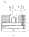
図1は、実施形態に従うFinFET100の簡略化した横断面図である。横断面は、(以降でより詳細に議論されることになる)チャネル108である、FinFETチャネルに垂直な平面でとられている。したがって、ソースおよびドレインは、図1中の断面によって示されない。というのは、ソースおよびドレインは、断面の平面の前および後に配置されることになるからである。
FIG. 1 is a simplified cross-sectional view of a
基板102上に形成されるのは、小さいバンドギャップバックゲートを設けるための層104である。図1の特定の実施形態では、基板102はシリコン(Si)であり、層104は、GaAsを含む半導体である。他の実施形態では、層104は、III−V族半導体化合物もしくはII−VI族半導体化合物、またはたとえばGeもしくはSiGeといった、IV族半導体元素または化合物などの、様々な半導体元素または半導体化合物を含む場合がある。いくつかの実施形態では、層104は、約0.5ミクロンの厚さで、0.1eVから2eVの範囲のバンドギャップを有する。いくつかの実施形態では、nタイプのFinFET100では、層104は、1×1019cm−3から1×1022cm−3の範囲の例示的なドーピング濃度で、多量にpタイプでドープされる(p++)。いくつかの実施形態では、pタイプのFinFET100では、層104は、1×1019cm−3から1×1022cm−3の範囲の例示的なドーピング濃度で、多量にnタイプでドープされる(n++)。いくつかの実施形態では、基板102は、シリコン以外の材料である場合がある。基板102の厚さは、いくつかの実施形態について50ミクロンよりも厚い場合がある。
Formed on the
層106は、層104より上に形成される。層106は、エッチストップとして働き、パンチスルーを低減する助けをし、層104により形成されるバックゲートに対するバリア層としても働く。層106は、ドープされない、nタイプFinFET100では1×1013cm−3から1×1017cm−3の範囲の例示的なドーピング濃度で軽くpタイプでドープされる、またはpタイプFinFET100では1×1013cm−3から1×1017cm−3の範囲の例示的なドーピング濃度のバックゲートで軽くnタイプでドープされる場合がある。図1の特定の実施形態では、層106は、AlAsを含む半導体であり、単結晶として形成される。他の実施形態では、層106は、たとえばIII−V族化合物などの他の半導体を含む場合がある。
層106は、層104のものよりも大きいバンドギャップを有する。したがって、「小バンドギャップ」および「大バンドギャップ」という用語は、それぞれ、層104および層106を記載するために使用することができる。いくつかの実施形態では、層106は、0.5eVから4eVの範囲のバンドギャップを有する。いくつかの実施形態では、層106は、高度に抵抗性であって、良好な電気的障壁を実現し、約100オングストロームの厚さを有することができる。
層106の上に、FinFET100を製造するために、他の構成要素が形成される。図1に示されるのは、チャネル108、ゲート誘電体110、ゲート112、および層間誘電体114である。図1の特定の実施形態では、チャネル108は、比較的小さいバンドギャップを有するGaAsを含む。すなわち、チャネル108のバンドギャップは、層106のものよりも小さく、層104のバンドギャップと同等である場合がある。いくつかの実施形態では、チャネル108は、0.1eVから2eVの範囲のバンドギャップを有する。チャネル108は、必ずしも層104のものと同じ材料を含む必要はなく、III−V族またはII−VI族化合物などの他の半導体材料を含む場合がある。
On top of
チャネル108が反転されると電子が多数キャリアであるnタイプFinFETでは、いくつかの実施形態のためのチャネル108は、比較的大きい電子移動度を有し、チャネル108が反転されると正孔が多数キャリアであるpタイプFinFETでは、いくつかの実施形態のためのチャネル108は、比較的大きい正孔移動度を有する。いくつかの実施形態では、チャネル108は、300オングストロームから1000オングストロームの範囲の厚さを有する。
In an n-type FinFET where the electrons are majority carriers when the
チャネル108は、フィン構造を形成するためにエッチングされる。説明しやすいように、FinFET100を作るすべての構成要素が図1の中に示されるわけではない。たとえば、ソース/ドレイン拡散は示されない。というのは、図1に表される視界は、2つのソース/ドレイン拡散が製造されることになるところの間の位置における、チャネル108に沿っているからである。
エッチストップとして働くことによって、層106は、チャネル108の高さのばらつきを減少することを可能にする。すなわち、GaAs層が層106の上に形成された後、チャネル108のフィン形状を形成するために、エッチングが施される。層106は、その表面においてエッチングプロセスを停止し、その結果、チャネル108の高さは、非常に良好に制御され、トランジスタ同士のチャネル高均一性をもたらす。
By acting as an etch stop, the
チャネル108のものよりも大きい層106のバンドギャップによって、従来技術のトランジスタと比較して、パンチスルー(ソース/ドレイン拡散のうちの一方から他方への不要な電流)がかなり減ることが期待される。さらに、層104は、バックゲートとして使用され、このことにより、チャネル電流の制御を拡大することを実現する。図1は、層104をバックゲートとして使用できるように、層104への電気接触をもたらすための、層104へのバックゲートコンタクト116を示しており、ここで、層間誘電体114を通って層104へトレンチがエッチングされ、その後導電材料が堆積される。FinFET100がオフ状態であるときに不要な漏れ電流を著しく減少させることができ、FinFET100がオン状態であるときに所望のオン状態チャネル電流を増加させることができるように、層104を備えるバックゲートは、FinFET100をオンおよびオフにする能力を向上する。
The band gap of
FinFET100をオンまたはオフにするため、電圧が、ゲート112および層104に提供され、ここで、電圧は、FinFETのタイプに依存する。たとえば、nタイプFinFET100をオンにするために、レール120の電圧により表される、好適に選択された第1の正の電圧をゲート112に印加することができ、レール122の電圧により表される、好適に選択された第2の正の電圧を、バックゲートコンタクト116を経由して層104に印加することができる。機能ユニット124および126は、ゲート112およびバックゲートコンタクト116をそれらのそれぞれのレールに結合するための回路要素を表す。接続線128および130は、ゲート112およびバックゲートコンタクト116への電気接続をもたらす、様々な金属層およびバイア(簡潔にするために図示せず)についての簡略表現である。図1にやはり示されるのは、層104およびゲート112へグランド(ゼロ)電圧を提供するグランドレール132である。nタイプFinFET100では、FinFET100をオフにするため、ゲート112およびバックゲートコンタクト116をグランド電圧に保持することができる。
A voltage is provided to
レール120のための電圧は、レール122のための電圧と異なる値であってよく、またはそれらが同じ値であってよく、その場合、レール120と122は、単一のレールを構成すると考えることができる。これらの電圧のうちの一方または両方は、他の回路要素のために使用される電力レール132の電圧により表される、ハイ電圧(VCC)と異なる値であってよい。
The voltage for
FinFET100がpタイプFinFETである場合では、機能ユニット124および126がゲート112をレール120にバックゲートコンタクト116をレール122に結合するように構成されるときにFinFET100をオンにすることができるが、ここで、レール120および122の電圧は、pタイプFinFETのために好適に選択される。いくつかの実施形態では、これらの電圧は、グランド電位であってよい。FinFET100をオフにするため、ゲート112およびバックゲートコンタクト116を電力レール132に結合することを実施することができる。
If
図6は、FinFET100をオンにするために、ゲート112およびバックゲートコンタクト116を、それらのそれぞれのレールに結合することを示す。ステップ602では、ゲート(112)は、FinFET100をオンにするために、第1のレール(たとえば、120)に結合される。バックゲートコンタクト166をレール122に結合することは、FinFET100のバックゲートを結合することと見なすことができ、ここで、バックゲートは、層104で識別される。ステップ604についてバックゲートという用語を使用すると、バックゲート(104)は、FinFET100をオンにするために第2のレール(たとえば、122)に結合される。ステップ602は、必ずしもステップ604の前に実施される必要はなく、両方のステップを本質的に同時に実施することができる。
FIG. 6 shows coupling the
図1に示されるのは、FinFET100の層104(バックゲート)およびソース/ドレイン拡散(図1に図示せず)の両方を、他のアクティブなデバイス(図示せず)のバックゲートおよびソース/ドレイン拡散から分離するための、深いトレンチ分離(DTI)領域118である。図示を簡潔にするために、DTI領域の一部のみが示されるが、実際には、DTI領域118は、FinFET100構造のすべてを他のアクティブなデバイスから電気的に分離するように延在し、または反復される。パッシベーション層または他の金属層などのさらなる層を、図1に示される構造より上に形成するが、そのようなさらなる集積層は当業界でよく知られており、図示を簡潔にするために示されない。
Shown in FIG. 1 is both the layer 104 (back gate) and source / drain diffusion (not shown in FIG. 1) of
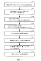
図2は、上に議論された実施形態に従うプロセスフロー図を示す。小さいバンドギャップの第1のGaAs層は、Si基板上に形成され(202)、その後、第1のGaAs層上に、大きいバンドギャップのAlAsエッチストップ層を形成する(204)。小さいバンドギャップの第2のGaAs層は、AlAsエッチストップ層上に形成され(206)、次いで、フィンチャネルを形成するためにエッチングされる(208)。ゲート誘電体は、フィンチャネルの上方に形成され(210)、その後、金属ゲートをエッチングして、形成する(212)。AlAs層を通って第1のGaAs層にトレンチがエッチングされ、バックゲートコンタクトが形成され(214)、DTI領域がSi基板を掘り下げて形成される(216)。FinFETを形成するために必要なすべてのステップは図2に示されないが、そのようなさらなるステップは当業界でよく知られている。 FIG. 2 shows a process flow diagram in accordance with the embodiment discussed above. A small bandgap first GaAs layer is formed on the Si substrate (202), and then a large bandgap AlAs etch stop layer is formed on the first GaAs layer (204). A small bandgap second GaAs layer is formed on the AlAs etch stop layer (206) and then etched (208) to form a fin channel. A gate dielectric is formed over the fin channel (210) and then formed by etching the metal gate (212). A trench is etched through the AlAs layer into the first GaAs layer, a back gate contact is formed (214), and a DTI region is formed by digging down the Si substrate (216). Although not all the steps necessary to form a FinFET are shown in FIG. 2, such additional steps are well known in the art.
いくつかの実施形態は、チャネル108の多数キャリア移動度を増加させるためのストレッサを含む場合がある。図3は、ストレッサ302および304を備えるFinFET300の横断面図を示す。図3の横断面図は、チャネル108に沿った平行な平面でとられ、ソース/ドレイン拡散306および308の横断面図を含む。図3は、側壁スペーサ310および312ならびにDTI領域314および316の横断面図をやはり含む。
Some embodiments may include a stressor to increase
ストレッサ302および304の組成は、一般的に、チャネル108のために使用される材料、およびFinFET300がnタイプ(nMOS)であるかpタイプ(pMOS)であるかに依存することになる。たとえば、チャネル108がSiチャネルである場合、いくつかの実施形態では、ストレッサ302および304は、FinFET300がpタイプであるとき、シリコンゲルマニウム合金(SiGe)を含むことができ、FinFET300がnタイプであるとき、炭化シリコン合金(SiC)を含むことができる。SiGe合金は、pタイプFinFETのための正孔移動度を増加させるように、チャネル108に圧縮応力を付与し、SiC合金は、nタイプFinFETのための電子移動度を増加させるように、引張応力を付与する。ストレッサ302および304は、層106から開始して、または層104から開始して、エピタキシャル成長させることができ、図3に示されるように、ソース/ドレイン拡散306および308の中に埋め込まれる。III−V族またはII−VI族半導体化合物、Ge、SiGe、グラフェンまたはカーボンナノチューブを有するチャネル材料では、ストレッサ302および304は、ストレッサの利点を最大化し、多数キャリア移動度を向上させるために異なる場合がある。
The composition of the
ストレッサ302および304は、層104および106の上に成長させる場合がある。なぜならば、これらの層は単結晶構造を有し、すなわち、それらは、各々均一の結晶格子を呈するからである。これを、従来型のSOI(シリコンオンインシュレータ)FinFETと比較すると、従来型のSOI FinFETは、そのフィンチャネルの下にバリアをやはり有するが、そこでのバリアはたとえば埋込酸化物層(BOX)などの単結晶ではない。そのような従来型のSOI FinFETでは、ストレッサは、BOXを通して良好に成長できない。
The
層106が単結晶であるので、ストレッサ302および304は、完全に層106を通して成長することができ、FinFET300の中に比較的深く埋め込まれ、比較的大きい体積をもたらす。埋込ストレッサ302および304についての比較的大きい体積は、チャネル108の多数キャリア移動度の増加に寄与するのに役に立つ。
Because
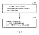
したがって、図4は、図2のフロー図に加えることができるプロセスステップを示す。ステップ402では、トレンチが層106の中に形成され、その後、形成されたトレンチの中にソース/ドレイン拡散に隣接してストレッサをエピタキシャル成長させる(404)。ステップ402は、同様に、層104の中にトレンチを形成することを含む場合がある。
Accordingly, FIG. 4 illustrates the process steps that can be added to the flow diagram of FIG. In
図5は、実施形態を適用できるワイヤレス通信システムを示す。図5は、基地局504A、504B、および504Cを備えるワイヤレス通信ネットワーク502を示す。図5は、セルラーフォン、タブレット、またはコンピュータもしくはコンピュータシステムなど、セルラーフォンネットワークに好適な何らかの他の種類の通信デバイスなどのモバイル通信デバイスであってよい、506と標示される通信デバイスを示す。通信デバイス506は、モバイルである必要はない。図5の特定の例では、通信デバイス506は、基地局504Cに関連付けられたセル内に位置する。矢印508および510は、それぞれアップリンクチャネルおよびダウンリンクチャネルを図式的に表しており、そのチャネルによって、通信デバイス506は基地局504Cと通信する。
FIG. 5 shows a wireless communication system to which the embodiment can be applied. FIG. 5 shows a
実施形態は、たとえば、通信デバイス506もしくは基地局504C、またはその両方に関連付けられるデータ処理システムにおいて用いられてもよい。図5は、本明細書において記載される実施形態が利用される場合がある数多くの適用例のうちの1つのみを示す。
Embodiments may be used, for example, in a data processing system associated with
様々な異なる技術および技法のいずれかを使用して、情報および信号を表すことができることを、当業者は了解するであろう。たとえば、上の記載全体にわたって参照される場合があるデータ、命令、コマンド、情報、信号、ビット、シンボル、およびチップは、電圧、電流、電磁波、磁場もしくは磁性粒子、光場もしくは光学粒子、またはそれらの任意の組合せによって表すことができる。 Those skilled in the art will appreciate that information and signals may be represented using any of a variety of different technologies and techniques. For example, data, instructions, commands, information, signals, bits, symbols, and chips that may be referred to throughout the above description are voltages, currents, electromagnetic waves, magnetic fields or magnetic particles, light fields or optical particles, or Can be represented by any combination of
さらに、当業者は、本明細書に開示された実施形態に関連して記載される様々な例示的な論理ブロック、モジュール、回路、およびアルゴリズムステップが、電子ハードウェア、コンピュータソフトウェア、または両方の組合せとして実装できることをさらに理解するであろう。ハードウェアとソフトウェアのこの互換性を明確に示すため、様々な例示の構成要素、ブロック、モジュール、回路、およびステップが、一般的にそれらの機能性の点で上に記載されてきた。そのような機能性がハードウェアまたはソフトウェアとして実装されるかどうかは、特定の用途および全体的なシステムに課せられる設計制約に依存する。当業者は、説明された機能を各々の特定の応用分野について様々な方式で実装してもよいが、そのような実装判断は、本開示の範囲からの逸脱を引き起こすと解釈されるべきではない。 Further, those skilled in the art will recognize that the various exemplary logic blocks, modules, circuits, and algorithm steps described in connection with the embodiments disclosed herein are electronic hardware, computer software, or a combination of both. You will further understand that it can be implemented as: To clearly illustrate this interchangeability of hardware and software, various illustrative components, blocks, modules, circuits, and steps have been described above generally in terms of their functionality. Whether such functionality is implemented as hardware or software depends upon the particular application and design constraints imposed on the overall system. Those skilled in the art may implement the described functionality in a variety of ways for each particular application, but such implementation decisions should not be construed as causing a departure from the scope of the present disclosure. .
本明細書に開示される実施形態に関して記載される方法、シーケンス、および/またはアルゴリズムは、ハードウェア中で直接、プロセッサにより実行されるソフトウェアモジュール中で、または2つの組合せで具現化することができる。ソフトウェアモジュールは、RAMメモリ、フラッシュメモリ、ROMメモリ、EPROMメモリ、EEPROMメモリ、レジスタ、ハードディスク、リムーバブルディスク、CD−ROM、または当技術分野において知られている任意の他の形の記憶媒体中に存在してもよい。例示的な記憶媒体は、プロセッサが記憶媒体から情報を読み込み、記憶媒体へ情報を書き込むことができるように、プロセッサと結合される。代替として、記憶媒体は、プロセッサと一体であってよい。 The methods, sequences, and / or algorithms described with respect to the embodiments disclosed herein may be implemented directly in hardware, in software modules executed by a processor, or in a combination of the two. . A software module resides in RAM memory, flash memory, ROM memory, EPROM memory, EEPROM memory, registers, hard disk, removable disk, CD-ROM, or any other form of storage medium known in the art May be. An exemplary storage medium is coupled to the processor such that the processor can read information from, and write information to, the storage medium. In the alternative, the storage medium may be integral to the processor.
したがって、本発明の実施形態は、バックゲートを有し、パンチスルーなしで、フィン高さのばらつきを減少させたFinFETのための方法を具現化するコンピュータ可読媒体を含むことができる。したがって、本発明は例示の例に限定されず、本明細書に記載される機能性を実施するための任意の手段は、本発明の実施形態に含まれる。 Accordingly, embodiments of the present invention can include a computer readable medium embodying a method for a FinFET having a back gate, no punchthrough, and reduced fin height variation. Accordingly, the invention is not limited to the illustrated examples and any means for performing the functionality described herein are included in embodiments of the invention.
上記の開示が本発明の例示の実施形態を示す一方で、添付される請求項により規定されるような、本発明の範囲から逸脱することなく、本明細書に様々な変形および変更を行うことができることに留意されたい。本明細書で記載される本発明の実施形態に従う方法クレームの機能、ステップ、および/または動作は、任意の特定の順序で実行される必要はない。さらに、本発明の要素は、単数形で記載され、特許請求される場合があるが、単数形への限定が明示的に言及されない限り、複数形が意図される。 While the above disclosure represents exemplary embodiments of the present invention, various modifications and changes may be made therein without departing from the scope of the invention as defined by the appended claims. Note that you can. The functions, steps, and / or actions of a method claim according to embodiments of the invention described herein need not be performed in any particular order. Further, although elements of the invention may be described and claimed in the singular, the plural is contemplated unless limitation to the singular is explicitly stated.
100 FinFET
102 基板
104 層
106 層
108 チャネル
110 ゲート誘電体
112 ゲート
114 層間誘電体
116 バックゲートコンタクト
118 深いトレンチ分離(DTI)領域
120 レール
122 レール
124 機能ユニット
126 機能ユニット
128 接続線
130 接続線
132 電力レール
300 FinFET
302 ストレッサ
304 ストレッサ
306 ソース/ドレイン拡散
308 ソース/ドレイン拡散
310 側壁スペーサ
312 側壁スペーサ
314 DTI領域
316 DTI領域
502 ワイヤレス通信ネットワーク
504A 基地局
504B 基地局
504C 基地局
506 通信デバイス
508 矢印
510 矢印
100 FinFET
102
302
Claims (30)
前記基板中に形成される第1の層を備えるバックゲートであって、前記第1の層が第1の半導体を備える、バックゲートと、
前記第1の層の上方に形成される第2の層であって、第2の半導体を備える第2の層と、
前記第2の層の上方に形成されるフィンチャネルであって、第3の半導体を備えるフィンチャネルと、
前記第2の層を通り、前記第1の層と電気接触する、バックゲートコンタクトと、
前記基板を掘り下げて形成される深いトレンチ分離領域と
を備え、
前記第1の半導体が第1のバンドギャップを有し、前記第3の半導体が第3のバンドギャップを有し、前記第2の半導体が前記第1のバンドギャップおよび第2のバンドギャップよりも大きい前記第2のバンドギャップを有する、
FinFET。 A substrate,
A back gate comprising a first layer formed in the substrate, wherein the first layer comprises a first semiconductor;
A second layer formed above the first layer, the second layer comprising a second semiconductor;
A fin channel formed above the second layer, the fin channel comprising a third semiconductor;
A back gate contact through the second layer and in electrical contact with the first layer;
A deep trench isolation region formed by digging down the substrate,
The first semiconductor has a first band gap, the third semiconductor has a third band gap, and the second semiconductor is more than the first band gap and the second band gap. Having a large second band gap;
FinFET.
前記誘電体層の上方に形成されるゲートと
をさらに備える、請求項1に記載のFinFET。 A dielectric layer formed above the fin channel;
The FinFET of claim 1, further comprising a gate formed above the dielectric layer.
前記FinFETをオンにする第2の電圧を提供するために前記バックゲートコンタクトに結合される第2のレールと
をさらに備える、請求項5に記載のFinFET。 A first rail coupled to the gate to provide a first voltage to turn on the FinFET;
The FinFET of claim 5, further comprising a second rail coupled to the back gate contact to provide a second voltage to turn on the FinFET.
をさらに備える、請求項1に記載のFinFET。 The FinFET of claim 1, further comprising a first stressor and a second stressor epitaxially grown in the second layer to provide stress to the fin channel.
前記フィンチャネルに隣接し、前記第2のストレッサに隣接する、第2のソース/ドレイン拡散と
をさらに備える、請求項8に記載のFinFET。 A first source / drain diffusion adjacent to the fin channel and adjacent to the first stressor;
9. The FinFET of claim 8, further comprising a second source / drain diffusion adjacent to the fin channel and adjacent to the second stressor.
前記FinFETをオンにする第2の電圧を提供するために前記バックゲートコンタクトに結合される第2のレールと
をさらに備える、請求項9に記載のFinFET。 A first rail coupled to the gate to provide a first voltage to turn on the FinFET;
The FinFET of claim 9, further comprising a second rail coupled to the back gate contact to provide a second voltage to turn on the FinFET.
基板の中に第1の半導体層を形成するステップと、
前記第1の半導体層の上方に第2の半導体層を形成するステップと、
前記第2の半導体層の上方に第3の半導体層を形成するステップと、
FinFETフィンチャネルを形成するために前記第3の半導体層をエッチングするステップと、
前記第2の半導体層を通って前記第1の半導体層までエッチングして、前記第1の半導体層への電気的なバックゲートコンタクトを形成するステップと、
前記基板に深いトレンチ分離領域を形成するステップと
を含み、
前記第1、第2、および第3の半導体層が、それぞれ第1のバンドギャップ、第2のバンドギャップ、および第3のバンドギャップを各々有し、前記第2のバンドギャップが前記第1のバンドギャップおよび前記第2のバンドギャップよりも大きい、
方法。 A method of manufacturing a FinFET, comprising:
Forming a first semiconductor layer in a substrate;
Forming a second semiconductor layer above the first semiconductor layer;
Forming a third semiconductor layer above the second semiconductor layer;
Etching the third semiconductor layer to form a FinFET fin channel;
Etching through the second semiconductor layer to the first semiconductor layer to form an electrical back gate contact to the first semiconductor layer;
Forming a deep trench isolation region in the substrate,
The first, second, and third semiconductor layers each have a first band gap, a second band gap, and a third band gap, respectively, and the second band gap is the first band gap. Greater than the band gap and the second band gap;
Method.
前記誘電体層の上方にゲートを形成するステップと
をさらに含む、請求項15に記載の方法。 Forming a dielectric layer over the FinFET fin channel;
The method of claim 15, further comprising forming a gate over the dielectric layer.
前記FinFETフィンチャネルに応力を提供するために、前記第1のトレンチの中に第1のストレッサをエピタキシャル成長させるステップと、
前記第2の層の中に第2のトレンチを形成するステップと、
前記FinFETフィンチャネルに応力を提供するために、前記第2のトレンチの中に第2のストレッサをエピタキシャル成長させるステップと
をさらに含む、請求項15に記載の方法。 Forming a first trench in the second layer;
Epitaxially growing a first stressor in the first trench to provide stress to the FinFET fin channel;
Forming a second trench in the second layer;
The method of claim 15, further comprising epitaxially growing a second stressor in the second trench to provide stress to the FinFET fin channel.
第2のソース/ドレイン拡散に隣接して前記第2のストレッサをエピタキシャル成長させるステップと
をさらに含む、請求項18に記載の方法。 Epitaxially growing the first stressor adjacent to a first source / drain diffusion;
The method of claim 18, further comprising epitaxially growing the second stressor adjacent to a second source / drain diffusion.
前記誘電体層の上方にゲートを形成するステップと
をさらに含む、請求項20に記載の方法。 Forming a dielectric layer over the FinFET fin channel;
21. The method of claim 20, further comprising forming a gate over the dielectric layer.
前記第1の層の中に前記第2のトレンチを形成するステップと
をさらに含む、請求項18に記載の方法。 Forming the first trench in the first layer;
The method of claim 18, further comprising forming the second trench in the first layer.
前記FinFETがpタイプである場合、前記第1の層を、1×1019cm−3から1×1022cm−3の範囲のドーピング濃度で、nタイプでドープする、
請求項15に記載の方法。 If the FinFET is n-type, the first layer is doped p-type with a doping concentration in the range of 1 × 10 19 cm −3 to 1 × 10 22 cm −3 ,
If the FinFET is p-type, the first layer is doped n-type with a doping concentration in the range of 1 × 10 19 cm −3 to 1 × 10 22 cm −3 ;
The method of claim 15.
前記FinFETがpタイプである場合、前記第2の層を、1×1013cm−3から1×1017cm−3の範囲のドーピング濃度で、nタイプでドープする、
請求項25に記載の方法。 If the FinFET is n-type, the second layer is doped p-type with a doping concentration in the range of 1 × 10 13 cm −3 to 1 × 10 17 cm −3 ,
If the FinFET is p-type, the second layer is doped n-type with a doping concentration in the range of 1 × 10 13 cm −3 to 1 × 10 17 cm −3 ;
26. The method of claim 25.
前記FinFETの前記ゲートを第1のレールに結合するステップと、
前記FinFETの前記バックゲートを第2のレールに結合するステップであって、前記バックゲートが、前記基板中に形成される第1の層を備え、第1の半導体を備えるステップと
を含み、
前記ゲートが、第2の層の上方に形成されるフィンチャネルの上方に形成され、前記第2の層が前記第1の層の上方に形成されて第2の半導体を備え、前記フィンチャネルが第3の半導体を備え、
前記第1の半導体が第1のバンドギャップを有し、前記第3の半導体が第3のバンドギャップを有し、前記第2の半導体が前記第1のバンドギャップおよび第2のバンドギャップよりも大きい前記第2のバンドギャップを有する、
方法。 A method of turning on a FinFET, wherein the FinFET comprises a gate, a back gate, and a substrate, the method comprising:
Coupling the gate of the FinFET to a first rail;
Coupling the back gate of the FinFET to a second rail, the back gate comprising a first layer formed in the substrate and comprising a first semiconductor;
The gate is formed above a fin channel formed above a second layer, the second layer is formed above the first layer and comprises a second semiconductor, the fin channel comprising Comprising a third semiconductor;
The first semiconductor has a first band gap, the third semiconductor has a third band gap, and the second semiconductor is more than the first band gap and the second band gap. Having a large second band gap;
Method.
Applications Claiming Priority (3)
| Application Number | Priority Date | Filing Date | Title |
|---|---|---|---|
| US14/179,311 US9236483B2 (en) | 2014-02-12 | 2014-02-12 | FinFET with backgate, without punchthrough, and with reduced fin height variation |
| US14/179,311 | 2014-02-12 | ||
| PCT/US2015/015426 WO2015123305A1 (en) | 2014-02-12 | 2015-02-11 | Finfet with backgate, without punchthrough, and with reduced fin height variation |
Publications (2)
| Publication Number | Publication Date |
|---|---|
| JP2017505545A true JP2017505545A (en) | 2017-02-16 |
| JP2017505545A5 JP2017505545A5 (en) | 2018-03-08 |
Family
ID=52577996
Family Applications (1)
| Application Number | Title | Priority Date | Filing Date |
|---|---|---|---|
| JP2016550526A Pending JP2017505545A (en) | 2014-02-12 | 2015-02-11 | FinFET with back gate and reduced punch height variation without punch-through |
Country Status (5)
| Country | Link |
|---|---|
| US (1) | US9236483B2 (en) |
| EP (1) | EP3105796A1 (en) |
| JP (1) | JP2017505545A (en) |
| CN (1) | CN105981174A (en) |
| WO (1) | WO2015123305A1 (en) |
Families Citing this family (10)
| Publication number | Priority date | Publication date | Assignee | Title |
|---|---|---|---|---|
| WO2016209284A1 (en) | 2015-06-26 | 2016-12-29 | Intel Corporation | High-mobility semiconductor source/drain spacer |
| US10411007B2 (en) | 2015-09-25 | 2019-09-10 | Intel Corporation | High mobility field effect transistors with a band-offset semiconductor source/drain spacer |
| US10446685B2 (en) | 2015-09-25 | 2019-10-15 | Intel Corporation | High-electron-mobility transistors with heterojunction dopant diffusion barrier |
| CN108028272B (en) * | 2015-09-25 | 2022-09-27 | 英特尔公司 | High electron mobility transistor with counter-doped dopant diffusion barrier |
| WO2017218015A1 (en) | 2016-06-17 | 2017-12-21 | Intel Corporation | High-mobility field effect transistors with wide bandgap fin cladding |
| US20180337228A1 (en) * | 2017-05-18 | 2018-11-22 | Taiwan Semiconductor Manufacturing Co., Ltd. | Novel seal ring for iii-v compound semiconductor-based devices |
| US10872794B2 (en) | 2017-06-20 | 2020-12-22 | Taiwan Semiconductor Manufacturing Co., Ltd. | Automatic in-line inspection system |
| WO2019005111A1 (en) * | 2017-06-30 | 2019-01-03 | Intel Corporation | Diverse transistor channel materials enabled by thin, inverse-graded, germanium-based layer |
| US20190371891A1 (en) * | 2018-06-01 | 2019-12-05 | Qualcomm Incorporated | Bulk layer transfer based switch with backside silicidation |
| US10756205B1 (en) | 2019-02-13 | 2020-08-25 | International Business Machines Corporation | Double gate two-dimensional material transistor |
Citations (5)
| Publication number | Priority date | Publication date | Assignee | Title |
|---|---|---|---|---|
| JP2002110963A (en) * | 2000-09-28 | 2002-04-12 | Toshiba Corp | Semiconductor device |
| JP2007287913A (en) * | 2006-04-17 | 2007-11-01 | Matsushita Electric Ind Co Ltd | Field effect transistor, and its manufacturing method |
| US20130011983A1 (en) * | 2011-07-07 | 2013-01-10 | Taiwan Semiconductor Manufacturing Company, Ltd. | In-Situ Doping of Arsenic for Source and Drain Epitaxy |
| US20130056795A1 (en) * | 2011-09-06 | 2013-03-07 | Taiwan Semiconductor Manufacturing Company, Ltd. | FinFET Design Controlling Channel Thickness |
| JP2013513250A (en) * | 2009-12-23 | 2013-04-18 | インテル コーポレイション | Non-planar germanium quantum well devices |
Family Cites Families (18)
| Publication number | Priority date | Publication date | Assignee | Title |
|---|---|---|---|---|
| US20060197129A1 (en) | 2005-03-03 | 2006-09-07 | Triquint Semiconductor, Inc. | Buried and bulk channel finFET and method of making the same |
| US7411252B2 (en) | 2005-06-21 | 2008-08-12 | International Business Machines Corporation | Substrate backgate for trigate FET |
| DE102005059231B4 (en) | 2005-12-12 | 2011-01-13 | Infineon Technologies Ag | A method of fabricating a compound semiconductor field effect transistor having a fin structure and compound semiconductor field effect transistor having a fin structure |
| US7569869B2 (en) | 2007-03-29 | 2009-08-04 | Intel Corporation | Transistor having tensile strained channel and system including same |
| US7485520B2 (en) | 2007-07-05 | 2009-02-03 | International Business Machines Corporation | Method of manufacturing a body-contacted finfet |
| US8120063B2 (en) | 2008-12-29 | 2012-02-21 | Intel Corporation | Modulation-doped multi-gate devices |
| CN101853882B (en) | 2009-04-01 | 2016-03-23 | 台湾积体电路制造股份有限公司 | There is the high-mobility multiple-gate transistor of the switch current ratio of improvement |
| US8796777B2 (en) * | 2009-09-02 | 2014-08-05 | Qualcomm Incorporated | Fin-type device system and method |
| US9245805B2 (en) * | 2009-09-24 | 2016-01-26 | Taiwan Semiconductor Manufacturing Company, Ltd. | Germanium FinFETs with metal gates and stressors |
| US8431994B2 (en) * | 2010-03-16 | 2013-04-30 | International Business Machines Corporation | Thin-BOX metal backgate extremely thin SOI device |
| US8796759B2 (en) | 2010-07-15 | 2014-08-05 | Taiwan Semiconductor Manufacturing Company, Ltd. | Fin-like field effect transistor (FinFET) device and method of manufacturing same |
| US8728881B2 (en) | 2011-08-31 | 2014-05-20 | Institute of Microelectronics, Chinese Academy of Sciences | Semiconductor device and method for manufacturing the same |
| US8624326B2 (en) | 2011-10-20 | 2014-01-07 | Taiwan Semiconductor Manufacturing Company, Ltd. | FinFET device and method of manufacturing same |
| US9099388B2 (en) | 2011-10-21 | 2015-08-04 | Taiwan Semiconductor Manufacturing Company, Ltd. | III-V multi-channel FinFETs |
| US8853781B2 (en) | 2011-12-16 | 2014-10-07 | International Business Machines Corporation | Rare-earth oxide isolated semiconductor fin |
| CN104170091B (en) | 2011-12-28 | 2017-05-17 | 英特尔公司 | Transistorized technology and the structure of stacked integrated circuit (IC)-components |
| US8836016B2 (en) | 2012-03-08 | 2014-09-16 | Taiwan Semiconductor Manufacturing Company, Ltd. | Semiconductor structures and methods with high mobility and high energy bandgap materials |
| US9171929B2 (en) | 2012-04-25 | 2015-10-27 | Taiwan Semiconductor Manufacturing Company, Ltd. | Strained structure of semiconductor device and method of making the strained structure |
-
2014
- 2014-02-12 US US14/179,311 patent/US9236483B2/en not_active Expired - Fee Related
-
2015
- 2015-02-11 WO PCT/US2015/015426 patent/WO2015123305A1/en active Application Filing
- 2015-02-11 JP JP2016550526A patent/JP2017505545A/en active Pending
- 2015-02-11 EP EP15706346.2A patent/EP3105796A1/en not_active Withdrawn
- 2015-02-11 CN CN201580007861.5A patent/CN105981174A/en active Pending
Patent Citations (5)
| Publication number | Priority date | Publication date | Assignee | Title |
|---|---|---|---|---|
| JP2002110963A (en) * | 2000-09-28 | 2002-04-12 | Toshiba Corp | Semiconductor device |
| JP2007287913A (en) * | 2006-04-17 | 2007-11-01 | Matsushita Electric Ind Co Ltd | Field effect transistor, and its manufacturing method |
| JP2013513250A (en) * | 2009-12-23 | 2013-04-18 | インテル コーポレイション | Non-planar germanium quantum well devices |
| US20130011983A1 (en) * | 2011-07-07 | 2013-01-10 | Taiwan Semiconductor Manufacturing Company, Ltd. | In-Situ Doping of Arsenic for Source and Drain Epitaxy |
| US20130056795A1 (en) * | 2011-09-06 | 2013-03-07 | Taiwan Semiconductor Manufacturing Company, Ltd. | FinFET Design Controlling Channel Thickness |
Also Published As
| Publication number | Publication date |
|---|---|
| WO2015123305A1 (en) | 2015-08-20 |
| CN105981174A (en) | 2016-09-28 |
| US20150228795A1 (en) | 2015-08-13 |
| EP3105796A1 (en) | 2016-12-21 |
| US9236483B2 (en) | 2016-01-12 |
Similar Documents
| Publication | Publication Date | Title |
|---|---|---|
| US9236483B2 (en) | FinFET with backgate, without punchthrough, and with reduced fin height variation | |
| US10164099B2 (en) | Device with diffusion blocking layer in source/drain region | |
| US9773868B2 (en) | Nanowire MOSFET with support structures for source and drain | |
| TWI695507B (en) | Crystalline multiple-nanosheet iii-v channel fets and methods of fabricating the same | |
| US9437681B2 (en) | Dual channel FinFET CMOS device with common strain-relaxed buffer and method for manufacturing thereof | |
| US8987835B2 (en) | FinFET with a buried semiconductor material between two fins | |
| US9728602B2 (en) | Variable channel strain of nanowire transistors to improve drive current | |
| US8853862B2 (en) | Contact structures for semiconductor transistors | |
| US20110049613A1 (en) | Accumulation type finfet, circuits and fabrication method thereof | |
| CN108962749B (en) | Insulated gate bipolar transistor device and semiconductor device | |
| US9620591B2 (en) | Semiconductor structures and methods for multi-level work function and multi-valued channel doping of nanowire transistors to improve drive current | |
| JP2018504775A (en) | Tunnel field effect transistor and manufacturing method thereof | |
| KR102441728B1 (en) | Vertical field effect device and method for fabricating the same | |
| CN106471624B (en) | Solid source diffusion junctions for fin-based electronics | |
| US9502583B2 (en) | Complementary high mobility nanowire neuron device | |
| US10283639B2 (en) | Semiconductor structure and method for forming the same | |
| Goh et al. | Gate-all-around In 0.53 Ga 0.47 As junctionless nanowire FET with tapered source/drain structure | |
| US10297691B2 (en) | Method for forming semiconductor device with P/N stacked layers | |
| US8704296B2 (en) | Trench junction field-effect transistor | |
| US20230088066A1 (en) | Fin-based field effect transistor (finfet) device with enhanced on-resistance and breakdown voltage | |
| KR101229187B1 (en) | Vertically pinched junction field effect transistor | |
| TW202406095A (en) | Monolithic complementary field-effect transistors having carbon-doped release layers | |
| CN111384146A (en) | TFET device | |
| CN102738174A (en) | Three-strained fully planar SOI (silicon on insulator) BiCMOS (bipolar complementary metal oxide semiconductor) integrated device and preparation method |
Legal Events
| Date | Code | Title | Description |
|---|---|---|---|
| A521 | Request for written amendment filed |
Free format text: JAPANESE INTERMEDIATE CODE: A523 Effective date: 20160815 |
|
| A521 | Request for written amendment filed |
Free format text: JAPANESE INTERMEDIATE CODE: A523 Effective date: 20180122 |
|
| A621 | Written request for application examination |
Free format text: JAPANESE INTERMEDIATE CODE: A621 Effective date: 20180122 |
|
| A977 | Report on retrieval |
Free format text: JAPANESE INTERMEDIATE CODE: A971007 Effective date: 20181017 |
|
| A131 | Notification of reasons for refusal |
Free format text: JAPANESE INTERMEDIATE CODE: A131 Effective date: 20181105 |
|
| A02 | Decision of refusal |
Free format text: JAPANESE INTERMEDIATE CODE: A02 Effective date: 20190603 |