JP2017227591A - Signal processing circuit, physical quantity detection device, attitude arithmetic unit, electronic apparatus, and movable body - Google Patents
Signal processing circuit, physical quantity detection device, attitude arithmetic unit, electronic apparatus, and movable body Download PDFInfo
- Publication number
- JP2017227591A JP2017227591A JP2016125419A JP2016125419A JP2017227591A JP 2017227591 A JP2017227591 A JP 2017227591A JP 2016125419 A JP2016125419 A JP 2016125419A JP 2016125419 A JP2016125419 A JP 2016125419A JP 2017227591 A JP2017227591 A JP 2017227591A
- Authority
- JP
- Japan
- Prior art keywords
- physical quantity
- signal
- signal processing
- posture calculation
- processing circuit
- Prior art date
- Legal status (The legal status is an assumption and is not a legal conclusion. Google has not performed a legal analysis and makes no representation as to the accuracy of the status listed.)
- Granted
Links
Images


Abstract
Description
本発明は、信号処理回路、物理量検出装置、姿勢演算装置、電子機器及び移動体に関する。 The present invention relates to a signal processing circuit, a physical quantity detection device, an attitude calculation device, an electronic device, and a moving object.
ロボットや車両等の移動体の姿勢に応じて各種の制御を行うシステムでは、移動体に取り付けられた角速度センサー等の各種のセンサーが検出するデータを用いて移動体の姿勢を演算する姿勢演算装置が用いられる。例えば、特許文献1には、3軸上の角速度、加速度及び地磁気をそれぞれ計測する角速度センサー、加速度センサー及び磁気センサーと、これらのセンサーの計測値を基にクォータニオンの推定値を算出する演算処理部とを備えた小型姿勢センサーが開示されている。
In a system that performs various controls according to the posture of a moving body such as a robot or a vehicle, a posture calculating device that calculates the posture of the moving body using data detected by various sensors such as an angular velocity sensor attached to the moving body Is used. For example,
しかしながら、従来の姿勢演算装置では、姿勢演算を行う処理部(CPU(Central Processing Unit)等)が、移動体に取り付けられた各種のセンサーと通信して3軸分のデータを取得し、取得した3軸分のデータを用いて姿勢演算を行うため、姿勢演算のレートを3軸分のデータの受信レートよりも高くすることができない。すなわち、従来の姿勢演算装置では、処理部とセンサーとの間の通信レートに依存して姿勢演算の周期が長くなり、姿勢演算の精度を向上させることが難しいという問題がある。 However, in a conventional posture calculation device, a processing unit (CPU (Central Processing Unit) or the like) that performs posture calculation communicates with various sensors attached to the moving body, acquires data for three axes, and acquires the data Since posture calculation is performed using data for three axes, the rate of posture calculation cannot be made higher than the reception rate of data for three axes. That is, the conventional posture calculation device has a problem that the posture calculation cycle becomes long depending on the communication rate between the processing unit and the sensor, and it is difficult to improve the accuracy of the posture calculation.
本発明は、以上のような問題点に鑑みてなされたものであり、本発明のいくつかの態様によれば、従来よりも姿勢演算の精度を向上させることが可能な信号処理回路、物理量検出装置及び姿勢演算装置を提供することができる。また、本発明のいくつかの態様によれば、当該姿勢演算装置を用いた電子機器及び移動体を提供することができる。 The present invention has been made in view of the above-described problems, and according to some aspects of the present invention, a signal processing circuit and a physical quantity detection capable of improving the accuracy of posture calculation as compared with the prior art. An apparatus and an attitude calculation device can be provided. In addition, according to some aspects of the present invention, it is possible to provide an electronic apparatus and a moving body using the posture calculation device.
本発明は前述の課題の少なくとも一部を解決するためになされたものであり、以下の態様または適用例として実現することが可能である。 SUMMARY An advantage of some aspects of the invention is to solve at least a part of the problems described above, and the invention can be implemented as the following aspects or application examples.
[適用例1]
本適用例に係る信号処理回路は、物理量検出素子の出力信号に基づいて第1の物理量信号を生成する検出回路と、前記第1の物理量信号を出力可能な第1の端子と、第2〜第N(N≧2)の物理量信号を入力可能な第2の端子と、前記第1〜第Nの物理量信号に基づいて姿勢演算を実行可能な姿勢演算部と、を含む。
[Application Example 1]
A signal processing circuit according to this application example includes a detection circuit that generates a first physical quantity signal based on an output signal of a physical quantity detection element, a first terminal that can output the first physical quantity signal, A second terminal capable of inputting an Nth (N ≧ 2) physical quantity signal; and an attitude calculation unit capable of executing an attitude calculation based on the first to Nth physical quantity signals.
従来の姿勢演算装置が外部装置と通信して第1〜第Nの物理量信号を取得して姿勢演算を実行するのに対して、本適用例に係る信号処理回路は、検出回路が生成した第1の物理量信号及び第2の端子を介して外部から取得した第2〜第Nの物理量信号に基づいて姿勢演算を実行する。すなわち、本適用例に係る信号処理回路は、外部装置と通信して第1の物理量信号を取得する必要がなく、また、外部から第2〜第Nの物理量信号を取得するのと並行して、検出回路が第1の物理量信号を生成することができるので、第1〜第Nの物理量信号を取得する時間を短くすることができる。その結果、本適用例に係る信号処理回
路によれば、従来よりも姿勢演算の周期が短くなり、姿勢演算の精度を向上させることができる。
Whereas the conventional posture calculation device communicates with an external device to acquire the first to Nth physical quantity signals and executes the posture calculation, the signal processing circuit according to this application example includes the first signal generated by the detection circuit. The posture calculation is executed based on the first physical quantity signal and the second to Nth physical quantity signals acquired from the outside via the second terminal. That is, the signal processing circuit according to this application example does not need to communicate with the external device to acquire the first physical quantity signal, and in parallel with the acquisition of the second to Nth physical quantity signals from the outside. Since the detection circuit can generate the first physical quantity signal, the time for acquiring the first to Nth physical quantity signals can be shortened. As a result, according to the signal processing circuit according to this application example, the period of posture calculation is shorter than the conventional one, and the accuracy of posture calculation can be improved.
また、本適用例に係る信号処理回路は、第1の端子から第1の物理量信号を出力可能であるとともに、第2の端子から第2〜第Nの物理量信号を入力可能であるので、第2の端子から入力される物理量信号を用いて姿勢演算を実行する回路(マスター)として機能することも、姿勢演算に用いられる物理量信号を出力する回路(スレーブ)として機能することもできる。従って、例えば、第1の信号処理回路の第2の端子と第2〜第Nの信号処理回路の各々の第1の端子とを電気的に接続することにより、第1の信号処理回路が第1の物理量信号を生成し、かつ、第2〜第Nの信号処理回路から第2〜第Nの物理量信号を取得して、姿勢演算を実行する姿勢演算装置を構成することができる。このような姿勢演算装置は、同じ構成のN個の信号処理回路を用いて実現することができるので、開発コストを削減することができる。
The signal processing circuit according to this application example can output the first physical quantity signal from the first terminal and can input the second to Nth physical quantity signals from the second terminal. It can function as a circuit (master) that executes posture calculation using a physical quantity signal input from the
[適用例2]
上記適用例に係る信号処理回路において、前記姿勢演算部は、クォータニオンを用いて前記姿勢演算を行ってもよい。
[Application Example 2]
In the signal processing circuit according to the application example described above, the posture calculation unit may perform the posture calculation using a quaternion.
[適用例3]
上記適用例に係る信号処理回路において、前記姿勢演算部は、前記姿勢演算として、前記第1〜第Nの物理量信号の各々を積分して第1〜第Nの角度を算出してもよい。
[Application Example 3]
In the signal processing circuit according to the application example, the attitude calculation unit may calculate the first to Nth angles by integrating each of the first to Nth physical quantity signals as the attitude calculation.
[適用例4]
上記適用例に係る信号処理回路において、前記姿勢演算部は、回転行列を用いて前記姿勢演算を行ってもよい。
[Application Example 4]
In the signal processing circuit according to the application example described above, the posture calculation unit may perform the posture calculation using a rotation matrix.
[適用例5]
上記適用例に係る信号処理回路は、前記物理量検出素子を駆動するための駆動信号を生成する駆動回路を含み、前記姿勢演算部は、前記駆動信号に基づくクロック信号を用いて前記姿勢演算を行ってもよい。
[Application Example 5]
The signal processing circuit according to the application example includes a drive circuit that generates a drive signal for driving the physical quantity detection element, and the posture calculation unit performs the posture calculation using a clock signal based on the drive signal. May be.
本適用例に係る信号処理回路によれば、物理量検出素子を駆動するための駆動信号は、CR発振回路やリングオシレーターなどを用いて発生させたクロック信号よりも周波数偏差が小さいので、駆動信号に基づくクロック信号を用いることにより、姿勢演算の精度を向上させることができる。例えば、相対的に周波数偏差が大きいクロック信号に基づいてサンプリングされた物理量信号を用いた姿勢演算において、相対的に周波数偏差が小さい駆動信号に基づくクロック信号を用いてサンプリング周期(時間積分の周期)を補正することにより、姿勢演算の精度を向上させることができる。 According to the signal processing circuit according to this application example, the drive signal for driving the physical quantity detection element has a smaller frequency deviation than the clock signal generated using a CR oscillation circuit, a ring oscillator, or the like. The accuracy of the posture calculation can be improved by using the clock signal based thereon. For example, in an attitude calculation using a physical quantity signal sampled based on a clock signal having a relatively large frequency deviation, a sampling period (time integration period) using a clock signal based on a drive signal having a relatively small frequency deviation By correcting this, the accuracy of posture calculation can be improved.
[適用例6]
上記適用例に係る信号処理回路は、前記第1〜第Nの物理量信号と第1〜第Nの検出軸との対応関係の設定情報を記憶する記憶部を含み、前記姿勢演算部は、前記設定情報を用いて前記姿勢演算を行ってもよい。
[Application Example 6]
The signal processing circuit according to the application example includes a storage unit that stores setting information of a correspondence relationship between the first to Nth physical quantity signals and the first to Nth detection axes, and the posture calculation unit includes the The posture calculation may be performed using setting information.
本適用例に係る信号処理回路によれば、設定情報を変更することにより、第1〜第Nの物理量信号と第1〜第Nの検出軸との対応関係を変更することができるので、汎用性の高い信号処理回路を実現することができる。 According to the signal processing circuit according to this application example, the correspondence between the first to Nth physical quantity signals and the first to Nth detection axes can be changed by changing the setting information. A highly reliable signal processing circuit can be realized.
[適用例7]
上記適用例に係る信号処理回路において、前記第1〜第Nの物理量信号の各々は角速度
信号であってもよい。
[Application Example 7]
In the signal processing circuit according to the application example described above, each of the first to Nth physical quantity signals may be an angular velocity signal.
[適用例8]
上記適用例に係る信号処理回路は、加速度検出素子及び地磁気検出素子の少なくとも一方の出力信号に基づいて、前記姿勢演算部による前記姿勢演算を補正する補正処理部を含んでもよい。
[Application Example 8]
The signal processing circuit according to the application example may include a correction processing unit that corrects the posture calculation performed by the posture calculation unit based on an output signal of at least one of the acceleration detection element and the geomagnetic detection element.
本適用例に係る信号処理回路によれば、姿勢演算の誤差(例えば、積分誤差)を加速度検出素子及び地磁気検出素子の少なくとも一方の出力信号を用いて補正することができるので、姿勢演算の精度を向上させることができる。 According to the signal processing circuit according to this application example, the posture calculation error (for example, the integration error) can be corrected using the output signal of at least one of the acceleration detection element and the geomagnetic detection element. Can be improved.
[適用例9]
本適用例に係る物理量検出装置は、上記のいずれかの信号処理回路と、物理量検出素子と、を備えている。
[Application Example 9]
A physical quantity detection device according to this application example includes any of the signal processing circuits described above and a physical quantity detection element.
従来の姿勢演算装置が外部装置と通信して第1〜第Nの物理量信号を取得して姿勢演算を実行するのに対して、本適用例に係る物理量検出装置では、信号処理回路が、検出回路が生成した第1の物理量信号及び第2の端子を介して外部から取得した第2〜第Nの物理量信号に基づいて姿勢演算を実行する。すなわち、本適用例に係る物理量検出装置は、外部装置と通信して第1の物理量信号を取得する必要がなく、また、外部から第2〜第Nの物理量信号を取得するのと並行して、検出回路が第1の物理量信号を生成することができるので、第1〜第Nの物理量信号を取得する時間を短くすることができる。その結果、本適用例に係る物理量検出装置によれば、従来よりも姿勢演算の周期が短くなり、姿勢演算の精度を向上させることができる。 Whereas the conventional posture calculation device communicates with an external device to acquire the first to Nth physical quantity signals and executes the posture calculation, in the physical quantity detection device according to this application example, the signal processing circuit detects Attitude calculation is executed based on the first physical quantity signal generated by the circuit and the second to Nth physical quantity signals acquired from the outside via the second terminal. That is, the physical quantity detection device according to this application example does not need to communicate with an external device to acquire the first physical quantity signal, and in parallel with acquiring the second to Nth physical quantity signals from the outside. Since the detection circuit can generate the first physical quantity signal, the time for acquiring the first to Nth physical quantity signals can be shortened. As a result, according to the physical quantity detection device according to this application example, the cycle of posture calculation is shorter than the conventional one, and the accuracy of posture calculation can be improved.
[適用例10]
本適用例に係る姿勢演算装置は、上記の物理量検出装置をN個備え、第1の前記物理量検出装置が備えている前記信号処理回路の前記第2の端子と、第2〜第Nの前記物理量検出装置の各々が備えている前記信号処理回路の前記第1の端子とが電気的に接続され、前記第1の前記物理量検出装置が備えている前記信号処理回路の前記姿勢演算部が前記姿勢演算を行う。
[Application Example 10]
The posture calculation device according to this application example includes N physical quantity detection devices described above, the second terminal of the signal processing circuit provided in the first physical quantity detection device, and the second to Nth Each of the physical quantity detection devices is electrically connected to the first terminal of the signal processing circuit, and the posture calculation unit of the signal processing circuit of the first physical quantity detection device includes the attitude calculation unit. Perform posture calculation.
本適用例によれば、第1の物理量検出装置が備える第1の信号処理回路が第1の物理量信号を生成し、かつ、第2の端子を介して、第2〜第Nの物理量検出装置がそれぞれ備える第2〜第Nの信号処理回路の第1の端子から出力される第2〜第Nの物理量信号を取得して、姿勢演算を実行する姿勢演算装置を構成することができる。 According to this application example, the first signal processing circuit included in the first physical quantity detection device generates the first physical quantity signal, and the second to Nth physical quantity detection devices via the second terminal. Can acquire the second to Nth physical quantity signals output from the first terminals of the second to Nth signal processing circuits, respectively, to constitute an attitude calculation device that executes the attitude calculation.
そして、本適用例に係る姿勢演算装置では、第1の物理量検出装置が備える信号処理回路は、外部装置と通信して第1の物理量信号を取得する必要がなく、また、第2〜第Nの物理量検出装置から第2〜第Nの物理量信号を取得するのと並行して、検出回路が第1の物理量信号を生成することができるので、第1〜第Nの物理量信号を取得する時間を短くすることができる。その結果、本適用例に係る姿勢演算装置によれば、従来よりも姿勢演算の周期が短くなり、姿勢演算の精度を向上させることができる。 In the posture calculation device according to this application example, the signal processing circuit included in the first physical quantity detection device does not need to communicate with the external device to acquire the first physical quantity signal, and the second to Nth. Since the detection circuit can generate the first physical quantity signal in parallel with acquiring the second to Nth physical quantity signals from the physical quantity detection device, the time for acquiring the first to Nth physical quantity signals Can be shortened. As a result, according to the posture calculation device according to this application example, the cycle of posture calculation is shorter than in the past, and the accuracy of posture calculation can be improved.
また、本適用例に係る姿勢演算装置は、同じ構成のN個の物理量検出装置を用いて実現することができるので、開発コストを削減することができる。 In addition, since the posture calculation device according to this application example can be realized using N physical quantity detection devices having the same configuration, the development cost can be reduced.
[適用例11]
本適用例に係る電子機器は、上記の姿勢演算装置を備えている。
[Application Example 11]
An electronic apparatus according to this application example includes the posture calculation device.
[適用例12]
本適用例に係る移動体は、上記の姿勢演算装置を備えている。
[Application Example 12]
The moving body according to this application example includes the posture calculation device.
これらの適用例によれば、従来よりも姿勢演算の精度を向上させることが可能な姿勢演算装置を備えているので、例えば、信頼性の高い電子機器及び移動体を実現することも可能である。 According to these application examples, since the posture calculation device capable of improving the accuracy of the posture calculation as compared with the related art is provided, for example, it is possible to realize a highly reliable electronic device and moving body. .
以下、本発明の好適な実施形態について図面を用いて詳細に説明する。なお、以下に説明する実施の形態は、特許請求の範囲に記載された本発明の内容を不当に限定するものではない。また以下で説明される構成の全てが本発明の必須構成要件であるとは限らない。 DESCRIPTION OF EMBODIMENTS Hereinafter, preferred embodiments of the present invention will be described in detail with reference to the drawings. The embodiments described below do not unduly limit the contents of the present invention described in the claims. Also, not all of the configurations described below are essential constituent requirements of the present invention.
以下では、物理量として角速度を検出する物理量検出装置(角速度検出装置)を例にとり説明する。 Hereinafter, a physical quantity detection device (angular velocity detection device) that detects an angular velocity as a physical quantity will be described as an example.
1.物理量検出装置
1−1.本実施形態
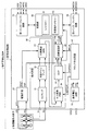
図1は、本実施形態の物理量検出装置の機能ブロック図である。本実施形態の物理量検出装置1は、物理量に関わるアナログ信号を出力する物理量検出素子(センサー素子)2と信号処理回路3を含んで構成されている。
1. Physical quantity detection device 1-1. First Embodiment FIG. 1 is a functional block diagram of a physical quantity detection device of the present embodiment. The physical
物理量検出素子2は、駆動電極と検出電極が配置された振動片を有し、一般的に、振動片のインピーダンスをできるだけ小さくして発振効率を高めるために、振動片は気密性が確保されたパッケージに封止されている。本実施形態では、物理量検出素子2は、T型の2つの駆動振動腕を有するいわゆるダブルT型の振動片を有する。
The physical
図2は、本実施形態の物理量検出素子2の振動片の平面図である。物理量検出素子2は
、例えば、Zカットの水晶基板により形成されたダブルT型の振動片を有する。水晶を材料とする振動片は、温度変化に対する共振周波数の変動が極めて小さいので、角速度の検出精度を高めることができるという利点がある。なお、図2におけるX軸、Y軸、Z軸は水晶の軸を示す。
FIG. 2 is a plan view of the resonator element of the physical
図2に示すように、物理量検出素子2の振動片は、2つの駆動用基部104a、104bからそれぞれ駆動振動腕101a、101bが+Y軸方向及び−Y軸方向に延出している。駆動振動腕101aの側面及び上面にはそれぞれ駆動電極112及び113が形成されており、駆動振動腕101bの側面及び上面にはそれぞれ駆動電極113及び112が形成されている。駆動電極112、113は、それぞれ、図1に示した信号処理回路3のDS端子,DG端子を介して駆動回路20に接続される。
As shown in FIG. 2, in the vibration piece of the physical
駆動用基部104a、104bは、それぞれ−X軸方向と+X軸方向に延びる連結腕105a、105bを介して矩形状の検出用基部107に接続されている。
The drive bases 104a and 104b are connected to a
検出振動腕102は、検出用基部107から+Y軸方向及び−Y軸方向に延出している。検出振動腕102の上面には検出電極114及び115が形成されており、検出振動腕102の側面には共通電極116が形成されている。検出電極114、115は、それぞれ、図1に示した信号処理回路3のS1端子,S2端子を介して検出回路30に接続される。また、共通電極116は接地される。
The
駆動振動腕101a、101bの駆動電極112と駆動電極113との間に駆動信号として交流電圧が与えられると、図3に示すように、駆動振動腕101a、101bは逆圧電効果によって矢印Bのように、2本の駆動振動腕101a、101bの先端が互いに接近と離間を繰り返す屈曲振動(励振振動)をする。
When an AC voltage is applied as a drive signal between the
この状態で、物理量検出素子2の振動片にZ軸を回転軸とした角速度が加わると、駆動振動腕101a、101bは、矢印Bの屈曲振動の方向とZ軸の両方に垂直な方向にコリオリの力を得る。その結果、図4に示すように、連結腕105a、105bは矢印Cで示すような振動をする。そして、検出振動腕102は、連結腕105a、105bの振動(矢印C)に連動して矢印Dのように屈曲振動をする。このコリオリ力に伴う検出振動腕102の屈曲振動と駆動振動腕101a、101bの屈曲振動(励振振動)とは位相が90°ずれている。
In this state, when an angular velocity with the Z axis as the rotation axis is applied to the vibration piece of the physical
ところで、駆動振動腕101a、101bが屈曲振動(励振振動)をするときの振動エネルギーの大きさ又は振動の振幅の大きさが2本の駆動振動腕101a、101bで等しければ、駆動振動腕101a、101bの振動エネルギーのバランスがとれており、物理量検出素子2に角速度がかかっていない状態では検出振動腕102は屈曲振動しない。ところが、2つの駆動振動腕101a、101bの振動エネルギーのバランスがくずれると、物理量検出素子2に角速度がかかっていない状態でも検出振動腕102に屈曲振動が発生する。この屈曲振動は漏れ振動と呼ばれ、コリオリ力に基づく振動と同様に矢印Dの屈曲振動であるが、駆動信号とは同位相である。
By the way, if the magnitude of the vibration energy or the magnitude of the vibration when the driving
そして、圧電効果によってこれらの屈曲振動に基づいた交流電荷が、検出振動腕102の検出電極114、115に発生する。ここで、コリオリ力に基づいて発生する交流電荷は、コリオリ力の大きさ(言い換えれば、物理量検出素子2に加わる角速度の大きさ)に応じて変化する。一方、漏れ振動に基づいて発生する交流電荷は、物理量検出素子2に加わる角速度の大きさに関係せず一定である。
Then, AC charges based on these bending vibrations are generated in the
なお、駆動振動腕101a、101bの先端には、駆動振動腕101a、101bより
も幅の広い矩形状の錘部103が形成されている。駆動振動腕101a、101bの先端に錘部103を形成することにより、コリオリ力を大きくするとともに、所望の共振周波数を比較的短い振動腕で得ることができる。同様に、検出振動腕102の先端には、検出振動腕102よりも幅の広い錘部106が形成されている。検出振動腕102の先端に錘部106を形成することにより、検出電極114、115に発生する交流電荷を大きくすることができる。
A
以上のようにして、物理量検出素子2は、Z軸を検出軸としてコリオリ力に基づく交流電荷(角速度成分)と、励振振動の漏れ振動に基づく交流電荷(振動漏れ成分)とを検出電極114、115を介して出力する。この物理量検出素子2は、角速度を検出する角速度センサーとして機能する。
As described above, the physical
図1に戻り、本実施形態の信号処理回路3は、基準電圧回路10、駆動回路20、検出回路30、姿勢演算部40、クロック生成回路50、記憶部60、第1インターフェース回路70及び第2インターフェース回路80を含んで構成されており、例えば、1チップの集積回路(IC:Integrated Circuit)であってもよい。なお、本実施形態の信号処理回路3は、これらの要素の一部を省略又は変更し、あるいは他の要素を追加した構成としてもよい。
Returning to FIG. 1, the
基準電圧回路10は、信号処理回路3のVDD端子より供給される電源電圧から基準電圧VR1,VR2などの定電圧や定電流を生成し、駆動回路20や検出回路30に供給する。
The
駆動回路20は、物理量検出素子2を駆動する(励振振動させる)ための駆動信号DRVを生成し、DS端子を介して物理量検出素子2の駆動電極112に供給する。また、駆動回路20は、物理量検出素子2の励振振動により駆動電極113に発生する発振電流がDG端子を介して入力され、この発振電流の振幅が一定に保持されるように駆動信号DRVの振幅レベルをフィードバック制御する。また、駆動回路20は、駆動信号DRVと位相が同じ検波信号SDETを生成し、検出回路30に出力する。
The
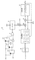
図5は、駆動回路20の構成例を示す図である。図5に示すように、駆動回路20は、I/V変換回路21、ローパスフィルター22、ハイパスフィルター23、コンパレーター24、全波整流回路25、積分器26、コンパレーター27及びコンパレーター28を含んで構成されている。なお、本実施形態の駆動回路20は、これらの要素の一部を省略又は変更し、あるいは他の要素を追加した構成としてもよい。
FIG. 5 is a diagram illustrating a configuration example of the
I/V変換回路21、ローパスフィルター22、ハイパスフィルター23、コンパレーター24、全波整流回路25、コンパレーター27及びコンパレーター28は、基準電圧回路10から供給される基準電圧VR1を基準に動作する。基準電圧VR1は、アナロググランド電圧であり、例えば、VDD端子から供給される電源電圧の1/2の電圧である。また、積分器26は、基準電圧回路10から供給される基準電圧VR2を基準に動作する。
The I / V conversion circuit 21, the low-pass filter 22, the high-pass filter 23, the comparator 24, the full-wave rectifier circuit 25, the comparator 27 and the comparator 28 operate based on the
I/V変換回路21は、物理量検出素子2の励振振動により発生し、DG端子を介して入力された発振電流を交流電圧信号に変換する。
The I / V conversion circuit 21 converts the oscillation current generated by the excitation vibration of the physical
ローパスフィルター22は、I/V変換回路21の出力信号の高周波成分を除去し、ハイパスフィルター23は、ローパスフィルター22の出力信号の低周波成分(オフセットなど)を除去する。ローパスフィルター22とハイパスフィルター23によってバンドパスフィルターが構成され、物理量検出素子2の励振振動により生じる信号を通過させる。
The low-pass filter 22 removes a high-frequency component of the output signal of the I / V conversion circuit 21, and the high-pass filter 23 removes a low-frequency component (such as an offset) of the output signal of the low-pass filter 22. The low-pass filter 22 and the high-pass filter 23 constitute a band-pass filter that allows a signal generated by the excitation vibration of the physical
コンパレーター24は、ハイパスフィルター23の出力信号の電圧を基準電圧VR1と比較して2値化信号を生成する。この2値化信号は、ハイレベルの電圧が積分器26の出力電圧であり、ローレベルの電圧がグラウンド電圧(0V)である。そして、コンパレーター24の出力信号は、駆動信号DRVとして、DS端子を介して物理量検出素子2に供給される。駆動信号DRVの周波数(駆動周波数)を物理量検出素子2の共振周波数と一致させることで、物理量検出素子2を安定発振させることができる。
The comparator 24 compares the voltage of the output signal of the high pass filter 23 with the reference voltage VR1, and generates a binarized signal. In this binarized signal, the high level voltage is the output voltage of the integrator 26 and the low level voltage is the ground voltage (0 V). The output signal of the comparator 24 is supplied to the physical
全波整流回路25は、I/V変換回路21の出力信号を整流(全波整流)して直流化された信号を出力する。 The full-wave rectification circuit 25 rectifies (full-wave rectification) the output signal of the I / V conversion circuit 21 and outputs a DC signal.
積分器26は、基準電圧VR2を基準に、全波整流回路25の出力電圧を積分して出力する。この積分器26の出力電圧は、全波整流回路25の出力電圧が高いほど(I/V変換回路21の出力信号の振幅が大きいほど)低くなる。従って、発振振幅が大きいほど、コンパレーター24の出力信号(駆動信号DRV)のハイレベルの電圧が低くなり、発振振幅が小さいほど、コンパレーター24の出力信号(駆動信号DRV)のハイレベルの電圧が高くなるので、発振振幅が一定に保持されるように自動利得制御(AGC:Auto Gain Control)がかかる。 The integrator 26 integrates and outputs the output voltage of the full-wave rectifier circuit 25 with reference to the reference voltage VR2. The output voltage of the integrator 26 becomes lower as the output voltage of the full-wave rectifier circuit 25 is higher (as the amplitude of the output signal of the I / V conversion circuit 21 is larger). Therefore, the higher the oscillation amplitude, the lower the high level voltage of the output signal (drive signal DRV) of the comparator 24, and the lower the oscillation amplitude, the higher level voltage of the output signal (drive signal DRV) of the comparator 24. Therefore, automatic gain control (AGC) is applied so that the oscillation amplitude is kept constant.
コンパレーター27は、ハイパスフィルター23の出力信号の電圧を増幅して2値化信号(方形波電圧信号)を生成し、検波信号SDETとして出力する。この検波信号SDETは、ハイレベルの電圧が電源電圧であり、ローレベルの電圧がグラウンド電圧(0V)である。 The comparator 27 amplifies the voltage of the output signal of the high pass filter 23 to generate a binarized signal (square wave voltage signal) and outputs it as a detection signal SDET. In the detection signal SDET, a high level voltage is a power supply voltage, and a low level voltage is a ground voltage (0 V).
コンパレーター28は、ハイパスフィルター23の出力信号の電圧を増幅して2値化信号(方形波電圧信号)を生成し、クロック信号CKFとして出力する。このクロック信号CKFは、ハイレベルの電圧が電源電圧であり、ローレベルの電圧がグラウンド電圧(0V)である。 The comparator 28 amplifies the voltage of the output signal of the high pass filter 23 to generate a binarized signal (square wave voltage signal) and outputs it as the clock signal CKF. In the clock signal CKF, a high level voltage is a power supply voltage, and a low level voltage is a ground voltage (0 V).
図1に戻り、検出回路30は、QVアンプ31、可変ゲインアンプ(PGA:Programmable Gain Amplifier)32、同期検波回路33、A/D(Analog to Digital)変換回路34及びDSP(Digital Signal Processor)35を含んで構成されている。なお、本実施形態の検出回路30は、これらの要素の一部を省略又は変更し、あるいは他の要素を追加した構成としてもよい。
Returning to FIG. 1, the
QVアンプ31は、S1端子を介して、物理量検出素子2の検出電極114から、角速度成分と振動漏れ成分を含む交流電荷(検出電流)が入力され、当該交流電荷に応じた電圧の信号を発生させる。また、QVアンプ31は、S2端子を介して、物理量検出素子2の検出電極115から、角速度成分と振動漏れ成分を含む交流電荷(検出電流)が入力され、当該交流電荷に応じた電圧の信号を発生させる。検出電極114からQVアンプ31に入力される交流電荷と検出電極114からQVアンプ31に入力される交流電荷は互いに逆位相(位相差が180°)であり、QVアンプ31から出力される2つの信号も互いに逆位相である。
The
可変ゲインアンプ32は、QVアンプ31から出力される2つの信号をそれぞれ増幅又は減衰させて、所望の電圧レベルの2つの信号を出力する。可変ゲインアンプ32から出力される2つの信号は、互いに逆位相である。
The
同期検波回路33は、駆動回路20が出力する検波信号SDETを用いて、可変ゲインアンプ32から出力される2つの信号(被検波信号)のそれぞれに含まれる角速度成分を
同期検波する。同期検波回路33は、例えば、検波信号SDETがハイレベルの時は可変ゲインアンプ32から出力される2つの信号をそのまま出力し、検波信号SDETがローレベルの時は可変ゲインアンプ32から出力される2つの信号をそれぞれ基準電圧VR1に対して反転した2つの信号を出力する回路として構成することができる。
The
A/D変換回路34は、クロック生成回路50が生成するクロック信号ADCCLKに同期して動作し、同期検波回路33が出力する2つの信号の差信号の電圧値をデジタルデータ(角速度データ)に変換して出力する。このA/D変換回路34から出力されるデジタルデータは、所定のレート(例えば、1.5kHz)で順次更新される。A/D変換回路34は、例えば、デルタシグマ型や逐次比較型のA/D変換回路であってもよい。
The A /
DSP35は、クロック生成回路50が生成するクロック信号DSPCLKに同期して動作し、A/D変換回路34から出力されるデジタルデータ(角速度データ)をフィルタリングする処理等を行う。DSP35による高速なデジタルフィルタリング処理等を実現するため、クロック信号DSPCLKの周波数は、A/D変換回路34の出力レート(例えば、1.5kHz)よりも十分高く、例えば、400kHz程度である。このDSP35から出力されるデジタルデータの値は、物理量検出素子2が検出した角速度ω1を表し、所定のレート(例えば、1.5kHz)で順次更新される。また、DSP35は、当該デジタルデータの値ω1が更新されたことを示すフラグ信号DRDYを出力する。
The
そして、DSP35から出力されるデジタルデータが検出回路30の出力データとなる。このように、検出回路30は、物理量検出素子2の出力信号に基づいて第1の物理量信号としてのデジタルデータ(角速度データ)を生成して出力する回路である。
The digital data output from the
姿勢演算部40は、第1〜第N(N≧2)の物理量信号に基づいて姿勢演算を実行可能である。本実施形態では、第1〜第Nの物理量信号は角速度信号であり、姿勢演算部40は、検出回路30(DSP35)から第1の物理量信号としてのデジタルデータ(角速度ω1)を取得し、記憶部60(レジスター61)から第2〜第Nの物理量信号としてのN−1個のデジタルデータ(角速度ω2〜ωN)を取得する。そして、姿勢演算部40は、記憶部60(不揮発性メモリー62)に記憶されている、第1〜第Nの物理量信号と第1〜第Nの検出軸との対応関係の設定情報を用いて、取得した第1〜第Nの物理量信号(角速度ω2〜ωN)の各々の検出軸を認識し、姿勢演算を行う。
The
本実施形態では、姿勢演算部40は、クォータニオンを用いて姿勢演算を行う。あるいは、姿勢演算部40は、姿勢演算として、第1〜第Nの物理量信号の各々を積分して第1〜第Nの角度を算出する。姿勢演算部40が、クォータニオンを用いて姿勢演算を行うか、姿勢演算として第1〜第Nの角度を算出するかは、記憶部60(不揮発性メモリー62)に記憶されている設定情報により決定される。また、本実施形態では、姿勢演算部40による姿勢演算を許可又は禁止に設定することが可能であり、姿勢演算部40は、許可に設定された場合に、クロック生成回路50が生成するクロック信号MCLKに同期して姿勢演算を行い、禁止に設定された場合は姿勢演算を行わない。
In the present embodiment, the
例えば、姿勢演算部40は、第1〜第3(N=3のケース)の物理量信号に基づいて3次元の姿勢演算を行うのであれば、検出回路30から、第1の物理量信号として角速度ω1を表すデジタルデータ(角速度データ)を所定の周期Δt(例えば、1/1.5kHz≒0.67ms)で順次取得する。また、姿勢演算部40は、記憶部60から、第2の物理量信号として角速度ω2を表すデジタルデータ(角速度データ)を所定の周期Δt(例えば、0.67ms)で順次取得する。さらに、姿勢演算部40は、記憶部60から、第3の物理量信号として角速度ω3を表すデジタルデータ(角速度データ)を周期Δt(例えば、0.67ms)で順次取得する。また、姿勢演算部40は、記憶部60(不揮発性
メモリー62)に記憶されている、第1〜第3の物理量信号と、第1〜第3の検出軸として互いに直交するx軸、y軸、z軸との対応関係の設定情報を用いて、例えば、第1の物理量信号としてのデジタルデータ(角速度ω1)をx軸回りの角速度データ(角速度ωx)と認識し、第2の物理量信号としてのデジタルデータ(角速度ω2)をy軸回りの角速度データ(角速度ωy)と認識し、第3の物理量信号としてのデジタルデータ(角速度ω3)をz軸回りの角速度データ(角速度ωz)と認識する。そして、姿勢演算部40は、x軸回りの角速度ωx(=ω1)、y軸回りの角速度ωy(=ω2)及びz軸回りの角速度ωz(=ω3)に基づき、クォータニオンを用いて姿勢演算を行うことができる。例えば、姿勢演算部40は、3軸分の角速度ωx,ωy,ωzを取得する毎に、式(1)に従ってクォータニオンqを更新し、更新したクォータニオンqを式(2)に従って正規化することにより、姿勢演算を行う。
For example, if the

あるいは、姿勢演算部40は、姿勢演算として、x軸回りの角速度ωx(=ω1)を積分してx軸の角度を算出し、y軸回りの角速度ωy(=ω2)を積分してy軸の角度を算出し、z軸回りの角速度ωz(=ω3)を積分してz軸の角度を算出することもできる。
Alternatively, the
ところで、本実施形態では、クロック信号ADCCLK、クロック信号DSPCLK及びクロック信号MCLKは、クロック生成回路50において、CR発振器やリングオシレーター等の発振回路(不図示)の出力信号に基づいて生成されるため、プロセス変動や環境変動により、物理量検出装置1の動作保証温度範囲(例えば、−40℃〜+85℃)において、例えば±1%程度の周波数偏差を有する。そのため、クロック信号ADCCLK及びクロック信号DSPCLKに同期して動作する検出回路30から出力されるデジタルデータの更新周期、すなわち、式(1)のΔtが±1%程度の誤差を有するため、姿勢演算の結果も±1%程度の誤差を有することになる。一方、物理量検出素子2は、良好な周波数温度特性を有する水晶等を材料として構成されるため、励振振動の周波数、すなわち、駆動信号DRVの周波数の偏差は極めて小さく、例えば±0.01%程度である。そこで、本実施形態では、姿勢演算部40は、駆動信号DRVに基づくクロック信号CKFを用いて姿勢演算を行う。
By the way, in the present embodiment, the clock signal ADCCLK, the clock signal DSPCLK, and the clock signal MCLK are generated in the
図6は、クォータニオンを用いて姿勢演算を行う姿勢演算部40の構成例を示す図である。図6に示すように、姿勢演算部40は、Dフリップフロップ41A,41B、NOT回路42、NOR回路43、カウンター44、乗算器45A,45B、変換部46、行列
演算部47、加算器48及び正規化部49を含んで構成されている。なお、図6では、姿勢演算の許可/禁止を制御するための構成は省略されている。
FIG. 6 is a diagram illustrating a configuration example of the
Dフリップフロップ41Aは、入力端子(D)にクロック信号CKFが入力され、クロック端子にクロック信号MCLKが入力される。Dフリップフロップ41Bは、入力端子(D)にDフリップフロップ41Aの出力端子(Q)から出力される信号が入力され、クロック端子にクロック信号MCLKが入力される。クロック信号CKFは、クロック信号MCLKと非同期であるため、Dフリップフロップ41A,41Bによってクロック信号MCLKに同期化される。Dフリップフロップ41Cは、入力端子(D)にDフリップフロップ41Bの出力端子(Q)から出力される信号(クロック信号MCLKに同期化されたクロック信号CKF)が入力され、クロック端子にクロック信号MCLKが入力される。Dフリップフロップ41Cの出力端子(Q)からは、フリップフロップ41Bの出力信号をクロック信号MCLKの1周期分遅らせた信号が出力される。
In the D flip-
NOT回路42は、Dフリップフロップ41Bの出力信号の電圧レベル(ローレベル/ハイレベル)を論理反転した信号を出力する。NOR回路43は、Dフリップフロップ41Cの出力信号とNOT回路42の出力信号の一方又は両方がハイレベルのときはローレベルとなり、Dフリップフロップ41Cの出力信号とNOT回路42の出力信号がともにローレベルのときにハイレベルとなる信号を出力する。すなわち、NOR回路43の出力信号には、クロック信号CKFがローレベルからハイレベルに変化する(立ち上がる)毎に、クロック信号MCLKの1周期分だけハイレベルとなる複数のパルスが含まれる。
The
カウンター44は、フラグ信号DRDYがローレベルのときに、NOR回路43の出力信号のパルス数をカウントしてカウント値を出力し、フラグ信号DRDYがハイレベルになるとカウント値を0にリセットする。このカウント値は、クロック信号CKFとフラグ信号DRDYとの周波数比を表している。
The counter 44 counts the number of pulses of the output signal of the NOR
乗算器45Aは、カウンター44が出力するカウント値と係数値COEFとの積を計算して出力する。係数値COEFは、記憶部60(不揮発性メモリー62)に記憶されており、式(3)で計算される定数値である。
The
式(3)において、GSは、検出回路30(GSは物理量検出素子2)の検出感度(単位:°/s/LSB)である。また、FREQは、クロック信号CKFの周波数(単位はHz)である。 In Expression (3), GS is the detection sensitivity (unit: ° / s / LSB) of the detection circuit 30 (GS is the physical quantity detection element 2). FREQ is the frequency (unit: Hz) of the clock signal CKF.
変換部46は、記憶部60(不揮発性メモリー62)に記憶されている、第1〜第3の物理量信号とx軸、y軸、z軸との対応関係の設定情報に基づいて、3軸の角速度データ(角速度ω1,ω2,ω3)をx軸回りの角速度ωx、y軸回りの角速度ωy及びz軸回りの角速度ωzに変換して出力する。
Based on the setting information of the correspondence relationship between the first to third physical quantity signals and the x-axis, y-axis, and z-axis stored in the storage unit 60 (non-volatile memory 62), the
行列演算部47は、クロック信号MCLKに同期して、x軸回りの角速度ωx、y軸回りの角速度及びz軸回りの角速度ωz(いずれも単位はLSB)と最新のクォータニオンq(各要素qw,qx,qy,qzの単位はラジアン)とを用いて、式(1)の右辺第1項中の行列積の部分を計算して出力する。
The
乗算器45Bは、行列演算部47の出力値と乗算器45Aの出力値との積を計算して出力する。この乗算器45Bの出力値は、式(1)の右辺第1項の計算値に相当する。
The
加算器48は、乗算器45Bの出力値と最新のクォータニオンqとの和を計算して出力する。この加算器48の出力値は、式(1)の計算値に相当する。
The
正規化部49は、クロック信号MCLKに同期して、加算器48の出力値を、その大きさが1になるように正規化して出力する。この正規化部49の出力値は、式(2)の計算値に相当し、最新のクォータニオンqとなる。
The normalizing
このように構成された姿勢演算部40は、クロック信号CKF(例えば、周波数偏差が±0.01%)とフラグ信号DRDY(例えば、周波数偏差が±1%)との周波数比を求め、当該周波数比を用いてΔtを補正し、式(1)及び式(2)に従ってクォータニオンqを計算するので、姿勢演算の精度が向上する。
The
図1に戻り、記憶部60は、レジスター61及び不揮発性メモリー62を有している。レジスター61には、第1インターフェース回路70及び第2インターフェース回路80を介した外部装置(第1の外部装置)との通信において使用されるアドレスやデータの情報が設定される。また、レジスター61には、第1インターフェース回路70及び第2インターフェース回路80を介した外部装置(第2〜第Nの外部装置)との通信によって取得したデータ(例えば、第2〜第Nの物理量信号としてのデジタルデータ)や姿勢演算部40による姿勢演算の結果(例えば、クォータニオンq)等が記憶される。
Returning to FIG. 1, the
不揮発性メモリー62には、駆動回路20や検出回路30に対する各種のトリミングデータ(調整データや補正データ)や第1インターフェース回路70及び第2インターフェース回路80を介した外部との通信を成立させるための各種の情報が記憶されている。不揮発性メモリー62は、例えば、MONOS(Metal Oxide Nitride Oxide Silicon)型メモリーやEEPROM(Electrically Erasable Programmable Read-Only Memory)として構成することができる。
In the
また、信号処理回路3の電源投入時(VDD端子の電圧が0Vから所望の電圧まで立ち上がる時)に、不揮発性メモリー62に記憶されている各種のトリミングデータがレジスター61に転送されて保持され、レジスター61に保持された各種のトリミングデータが駆動回路20や検出回路30に供給される。
When the
また、前述の通り、本実施形態では、記憶部60(不揮発性メモリー62)には、第1〜第Nの物理量信号と第1〜第Nの検出軸との対応関係の設定情報が記憶されており、姿勢演算部40は、当該設定情報を用いて姿勢演算を行う。
In addition, as described above, in the present embodiment, the storage unit 60 (nonvolatile memory 62) stores setting information on the correspondence relationship between the first to Nth physical quantity signals and the first to Nth detection axes. The
第1インターフェース回路70は、XCS端子、SCLK端子、MOSI端子及びMISO端子と電気的に接続されており、これらの端子を介して第1の外部装置と通信するための回路である。第1インターフェース回路70を介した通信では、第1の外部装置がマスターとして機能し、物理量検出装置1(信号処理回路3)がスレーブとして機能する。そして、第1の外部装置は、第1インターフェース回路70を介して、レジスター61の所定のアドレスにデータを書き込むことや、レジスター61の所定のアドレスからデータを読み出すことや、各種のコマンドを送信して信号処理回路3の動作を制御することができる。
The
本実施形態では、第1インターフェース回路70は、SPI(Serial Peripheral Interface)インターフェース回路とI2C(Inter-Integrated Circuit)インターフェース
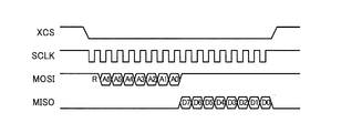
回路のいずれか一方として機能する。例えば、第1インターフェース回路70は、XCS端子がローレベルのときは、SPIインターフェース回路として機能し、SCLK端子を介してクロック信号が入力され、MOSI端子を介してデータ信号が入力され、MISO端子を介してデータ信号が出力される。また、第1インターフェース回路70は、XCS端子がハイレベルのときは、I2Cインターフェース回路として機能し、SCLK端子を介してクロック信号が入力され、MOSI端子を介してデータ信号が入出力される。図7〜図9に、第1インターフェース回路70がSPIインターフェース回路として機能するときの、第1インターフェース回路70を介した通信フォーマット(XCS端子、SCLK端子、MOSI端子及びMISO端子の信号波形)の一例を示す。図7は、第1の外部装置が、レジスター61の所定のアドレスにデータを書き込むときの通信フォーマットである。また、図8は、第1の外部装置が、レジスター61の所定のアドレスからデータを読み出すときの通信フォーマットである。また、図9は、第1の外部装置が所定のコマンドを送信するときの通信フォーマットである。図7〜図9において、Rは読み出しビット、Wは書き込みビット、A6〜A0は7ビットアドレス、D7〜D0は8ビットデータである。
In the present embodiment, the
第2インターフェース回路80は、MSCK端子及びMSDA端子と電気的に接続されており、これらの端子を介して第2〜第Nの外部装置と通信するための回路である。第2インターフェース回路80を介した通信では、物理量検出装置1(信号処理回路3)がマスターとして機能し、第2〜第Nの外部装置がスレーブとして機能する。そして、物理量検出装置1(信号処理回路3)は、第2インターフェース回路80を介して、第2〜第Nの外部装置が有する記憶部(レジスター)の所定のアドレスにデータを書き込むことや、第2〜第Nの外部装置が有する記憶部(レジスター)の所定のアドレスからデータを読み出すことができる。
The
本実施形態では、第2インターフェース回路80は、I2Cインターフェース回路として機能し、MSCK端子を介してクロック信号が出力され、MSDA端子を介してデータ信号が入出力される。図10及び図11に、第2インターフェース回路80を介した通信フォーマット(MSCK端子及びMSDA端子の信号波形)の一例を示す。図10は、物理量検出装置1(信号処理回路3)が、第2〜第Nの外部装置が有する記憶部(レジスター)の所定のアドレスにデータを書き込むときの信号波形である。また、図11は、物理量検出装置1(信号処理回路3)が、第2〜第Nの外部装置が有する記憶部(レジスター)の所定のアドレスからデータを読み出すときの信号波形である。図10及び図11において、Startはスタートコンディション、Stopはストップコンディション、Restartはリスタートコンディション、ACKはアクノリッジビット、NACKはノンアクノリッジビット、Rは読み出しビット、Wは書き込みビット、A7〜A0は8ビットのレジスターアドレス(MI2CRAD[7:0])、A6〜A0は7ビットのスレーブアドレス(MI2CSAD[6:0])、D7〜D0は7ビットの書き込みデータ又は読み出しデータである。
In the present embodiment, the
第1インターフェース回路70を介した第1の外部装置との間の通信は、レジスター61に記憶される各種の情報に基づいて行われる。また、第2インターフェース回路80を介した第2〜第Nの外部装置との間の通信は、レジスター61及び不揮発性メモリー62に記憶される各種の情報に基づいて行われる。
Communication with the first external device via the
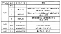
図12は、レジスター61のアドレスマップの一例を示す図である。図12では、アドレスマップの一部のみが示されており、「R/W」の欄において、「R」は読み出しのみ可能であり、「R/W」は読み出し及び書き込みが可能であり、「W(C)」はコマンドであることを表している。また、図13は、図12に示した書き込み可能な各アドレスのデータ構成を示す図である。
FIG. 12 is a diagram showing an example of an address map of the
第1の外部装置は、例えば、図8に示した通信フォーマットに従い、第1インターフェース回路70を介して、レジスター61のアドレス0x0A(レジスターRDGR)から第1の物理量信号としてのデジタルデータ(角速度データ)を読み出すことができる。このように、物理量検出装置1(信号処理回路3)は、第1の外部装置からの読み出し要求に応じて、MISO端子(「第1の端子」の一例)から第1の物理量信号としてのデジタルデータ(角速度データ)を出力可能に構成されている。なお、第1インターフェース回路70がI2Cインターフェース回路として機能する場合は、第1の外部装置からの読み出し要求に応じて、MOSI端子(「第1の端子」の他の一例)から第1の物理量信号としてのデジタルデータ(角速度データ)が出力される。
The first external device, for example, in accordance with the communication format shown in FIG. 8, digital data (angular velocity data) as the first physical quantity signal from the address 0x0A (register RDGR) of the
また、第1の外部装置は、例えば、図7に示した通信フォーマットに従い、第1インターフェース回路70を介して、レジスター61のアドレス0x11(レジスターMCTL)に姿勢演算部40や第2インターフェース回路80の設定情報を書き込むことができる。図13に示すように、アドレス0x11(レジスターMCTL)において、ビット2は、第2インターフェース回路80のマニュアル動作を書き込み又は読み出しに設定するためのビットであり、ビット1は、第2インターフェース回路80のマニュアル動作の許可又は禁止を設定するためのビットであり、ビット0は、姿勢演算部40による姿勢演算の許可又は禁止を設定するためのビットである。さらに、第1の外部装置は、例えば、図8に示した通信フォーマットに従い、第1インターフェース回路70を介して、レジスター61のアドレス0x11(レジスターMCTL)から当該設定情報を読み出すこともできる。
Also, the first external device, for example, in accordance with the communication format shown in FIG. 7, the
また、第1の外部装置は、例えば、図8に示した通信フォーマットに従い、第1インターフェース回路70を介して、レジスター61のアドレス0x12(レジスターRDAG)から姿勢演算部40の演算結果情報(3軸角度データ又は姿勢データ(例えば、クォータニオンq))を読み出すことができる。
Also, the first external device, for example, according to the communication format shown in FIG. 8, calculates the calculation result information (three axes) from the address 0x12 (register RDAG) of the
また、第1の外部装置は、例えば、図9に示した通信フォーマットに従い、第1インターフェース回路70に、レジスター61のアドレス0x13(レジスターAGRS)を指定して、姿勢演算部40の演算結果情報(3軸角度データ又は姿勢データ)をリセットするためのコマンドを送信することができる。第1インターフェース回路70は、当該コマンドを受信すると、姿勢演算部40の演算結果情報及び姿勢演算部40の動作を初期化する。
Further, the first external device, for example, specifies the address 0x13 (register AGRS) of the
また、第1の外部装置は、例えば、図9に示した通信フォーマットに従い、第1インターフェース回路70に、レジスター61のアドレス0x14(レジスターMI2CST)を指定して、第2インターフェース回路80のマニュアル動作を開始させるためのコマンドを送信することができる。
Also, the first external device designates the address 0x14 (register MI2CST) of the
また、第1の外部装置は、例えば、図7に示した通信フォーマットに従い、第1インターフェース回路70を介して、レジスター61のアドレス0x15(レジスターMI2CSAD)に、第2インターフェース回路80のマニュアル動作による通信で用いられるスレーブアドレス(図10及び図11のスレーブアドレスMI2CSAD[6:0])を書き込むことができる。図13に示すように、アドレス0x15(レジスターMI2CSAD)において、ビット6〜0は、7ビットのスレーブアドレスを設定するためのビットである。さらに、第1の外部装置は、例えば、図8に示した通信フォーマットに従い、第1インターフェース回路70を介して、レジスター61のアドレス0x15(レジスターMI2CSAD)から当該スレーブアドレスを読み出すこともできる。
Further, the first external device communicates by manual operation of the
また、第1の外部装置は、例えば、図7に示した通信フォーマットに従い、第1インターフェース回路70を介して、レジスター61のアドレス0x16(レジスターMI2CRAD)に、第2インターフェース回路80のマニュアル動作による通信で用いられるレジスターアドレス(図10及び図11のレジスターアドレスMI2CRAD[7:0])を書き込むことができる。図13に示すように、アドレス0x16(レジスターMI2CRAD)において、ビット7〜0は、8ビットのレジスターアドレスを設定するためのビットである。さらに、第1の外部装置は、例えば、図8に示した通信フォーマットに従い、第1インターフェース回路70を介して、レジスター61のアドレス0x16(レジスターMI2CRAD)から当該レジスターアドレスを読み出すこともできる。
Also, the first external device communicates by manual operation of the
また、第1の外部装置は、例えば、図7に示した通信フォーマットに従い、第1インターフェース回路70を介して、レジスター61のアドレス0x17(レジスターMI2CDAD)に、第2インターフェース回路80のマニュアル動作による通信で用いられる書き込みデータ(図10の書き込みデータMI2CDAD[7:0])を書き込むことができる。図13に示すように、アドレス0x17(レジスターMI2CDAD)において、ビット7〜0は、8ビットの書き込みデータを設定するためのビットである。さらに、第1の外部装置は、例えば、図8に示した通信フォーマットに従い、第1インターフェース回路70を介して、レジスター61のアドレス0x17(レジスターMI2CDAD)から当該書き込みデータを読み出すこともできる。
Further, the first external device performs communication by manual operation of the
また、第1の外部装置は、例えば、図8に示した通信フォーマットに従い、第1インターフェース回路70を介して、レジスター61のアドレス0x18(レジスターMI2CRD)から、第2インターフェース回路80のマニュアル動作による通信で第2〜第Nの外部装置から取得した読み出しデータを読み出すことができる。
Further, the first external device performs communication by manual operation of the
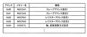
図14は、不揮発性メモリー62のアドレスマップの一例を示す図である。図14では、アドレスマップの一部のみが示されている。また、図15は、図14に示した各アドレスのデータ構成を示す図である。なお、図14及び図15は、信号処理回路3が、第2インターフェース回路80を介して、第2の外部装置及び第3の外部装置と通信する場合(N=3のケース)の例である。
FIG. 14 is a diagram illustrating an example of an address map of the
図14及び図15に示すように、不揮発性メモリー62において、アドレス0x01(メモリーMI2CSA1)のビット6〜0には、第2の外部装置のスレーブアドレスが記憶され、アドレス0x02(メモリーMI2CSA2)のビット6〜0には、第3の外部装置のスレーブアドレスが記憶されている。また、不揮発性メモリー62において、アドレス0x03(メモリーMI2CRA1)のビット7〜0には、第2の外部装置のレジスターにおいて、第2の物理量信号としてのデジタルデータ(角速度ω2)が記憶されるレジスターアドレスが記憶され、アドレス0x04(メモリーMI2CRA2)のビット7〜0には、第3の外部装置のレジスターにおいて、第3の物理量信号としてのデジタルデータ(角速度ω3)が記憶されるレジスターアドレスが記憶されている。
As shown in FIGS. 14 and 15, in the
物理量検出装置1(信号処理回路3)は、レジスター61のアドレス0x11のビット0(MCTL[0])が1(姿勢演算部40による姿勢演算の許可)に設定されている場合、図11に示した通信フォーマットに従い、スレーブアドレスMI2CSAD[6:0]としてアドレス0x01に記憶されているスレーブアドレスを用い、レジスターアドレスMI2CRAD[7:0]としてアドレス0x03に記憶されているレジスターアドレスを用いることにより、第2インターフェース回路80を介して、第2の外部装置から、読み出しデータMI2CRD[6:0]として第2の物理量信号としてのデジタルデータ(角速度ω2)を読み出す。また、物理量検出装置1(信号処理回路3)は、図11に示した通信フォーマットに従い、スレーブアドレスMI2CSAD[6:0]としてアドレ
ス0x02に記憶されているスレーブアドレスを用い、レジスターアドレスMI2CRAD[7:0]としてアドレス0x04に記憶されているレジスターアドレスを用いることにより、第2インターフェース回路80を介して、第3の外部装置から、読み出しデータMI2CRD[6:0]として第3の物理量信号としてのデジタルデータ(角速度ω3)を読み出す。このように、物理量検出装置1(信号処理回路3)は、MSDA端子(「第2の端子」の一例)から第2〜第Nの物理量信号としてのデジタルデータ(角速度データ)に構成されている。
The physical quantity detection device 1 (signal processing circuit 3) is shown in FIG. 11 when the bit 0 (MCTL [0]) of the address 0x11 of the
また、不揮発性メモリー62において、アドレス0x04(メモリーAXISCTL)のビット2は、姿勢演算部40による姿勢演算として角度演算とクォータニオン演算のいずれか一方を設定するためのビットである。姿勢演算部40は、アドレス0x04のビット2が0であれば角度演算を行い、アドレス0x04のビット2が1であればクォータニオン演算を行う。
In the
また、不揮発性メモリー62において、アドレス0x04(メモリーAXISCTL)のビット1〜0は、第1の物理量信号としてのデジタルデータ(角速度ω1)の検出軸(物理量検出素子2の検出軸)を設定するためのビットである。姿勢演算部40は、アドレス0x04のビット1〜0が0であれば、第1の物理量信号としてのデジタルデータ(角速度ω1)をx軸回りの角速度データ(角速度ωx)と認識する。この場合、姿勢演算部40は、第2の物理量信号としてのデジタルデータ(角速度ω2)をy軸回りの角速度データ(角速度ωy)と認識し、第3の物理量信号としてのデジタルデータ(角速度ω3)をz軸回りの角速度データ(角速度ωz)と認識する。また、姿勢演算部40は、アドレス0x04のビット1〜0が1であれば、第1の物理量信号としてのデジタルデータ(角速度ω1)をy軸回りの角速度データ(角速度ωy)と認識する。この場合、姿勢演算部40は、第2の物理量信号としてのデジタルデータ(角速度ω2)をx軸回りの角速度データ(角速度ωx)と認識し、第3の物理量信号としてのデジタルデータ(角速度ω3)をz軸回りの角速度データ(角速度ωz)と認識する。また、姿勢演算部40は、アドレス0x04のビット1〜0が2であれば、第1の物理量信号としてのデジタルデータ(角速度ω1)をz軸回りの角速度データ(角速度ωz)と認識する。この場合、姿勢演算部40は、第2の物理量信号としてのデジタルデータ(角速度ω2)をx軸回りの角速度データ(角速度ωx)と認識し、第3の物理量信号としてのデジタルデータ(角速度ω3)をy軸回りの角速度データ(角速度ωy)と認識する。このように、不揮発性メモリー62において、アドレス0x04のビット1〜0は、第1〜第3の物理量信号とx軸、y軸、z軸との対応関係の設定情報である。
In the
以上に説明したように、従来の姿勢演算装置が外部装置と通信して第1〜第Nの物理量信号を取得して姿勢演算を実行するのに対して、本実施形態の物理量検出装置1(信号処理回路3)は、検出回路30が出力する第1の物理量信号及びMSDA端子を介して外部装置から取得した第2〜第Nの物理量信号に基づいて姿勢演算を実行する。すなわち、本実施形態の物理量検出装置1(信号処理回路3)では、検出回路30が第1の物理量信号を出力するので、外部装置と通信して第1の物理量信号を取得する必要がなく、また、外部装置から第2〜第Nの物理量信号を取得するのと並行して、検出回路30が第1の物理量信号を生成することができるので、第1〜第Nの物理量信号を取得する時間を短くすることができる。その結果、本実施形態の物理量検出装置1(信号処理回路3)によれば、従来よりも姿勢演算の周期が短くなり、姿勢演算の精度を向上させることができる。
As described above, the conventional posture calculation device communicates with an external device to acquire the first to Nth physical quantity signals and executes the posture calculation, whereas the physical quantity detection device 1 ( The signal processing circuit 3) performs posture calculation based on the first physical quantity signal output from the
また、本実施形態の物理量検出装置1では、信号処理回路3は、MISO端子あるいはMOSI端子から第1の物理量信号を出力可能であるとともに、MSDA端子から第2〜第Nの物理量信号を入力可能であるので、MSDA端子から入力される物理量信号を用いて姿勢演算を実行する回路(マスター)として機能することも、姿勢演算に用いられる物
理量信号を出力する回路(スレーブ)として機能することもできる。従って、例えば、第1の信号処理回路3のMSDA端子と第2〜第Nの信号処理回路3の各々のMOSI端子とを電気的に接続することにより、第1の信号処理回路3が第1の物理量信号を生成し、かつ、第2〜第Nの信号処理回路3から第2〜第Nの物理量信号を取得して、姿勢演算を実行する姿勢演算装置を構成することができる。このような姿勢演算装置は、同じ構成のN個の信号処理回路3を用いて実現することができるので、開発コストを削減することができる。
In the physical
また、本実施形態の物理量検出装置1(信号処理回路3)によれば、物理量検出素子2を駆動するための駆動信号DRVは、クロック生成回路50が発生させるクロック信号ADCCLK,DSPCLKよりも周波数偏差が小さいので、駆動信号DRVに基づくクロック信号CKFを用いることにより、姿勢演算の精度を向上させることができる。すなわち、本実施形態の物理量検出装置1(信号処理回路3)によれば、相対的に周波数偏差が大きいクロック信号ADCCLKに基づいてサンプリングされた物理量信号を用いた姿勢演算において、相対的に周波数偏差が小さい駆動信号DRVに基づくクロック信号CKFを用いてサンプリング周期(時間積分の周期)Δtを補正することにより、姿勢演算の精度を向上させることができる。
Further, according to the physical quantity detection device 1 (signal processing circuit 3) of the present embodiment, the drive signal DRV for driving the physical
本実施形態によれば、記憶部60(例えば、図14及び図15において、不揮発性メモリー62のアドレス0x04)に記憶される設定情報を変更することにより、第1〜第Nの物理量信号と第1〜第Nの検出軸との対応関係を変更することができるので、汎用性の高い物理量検出装置1(信号処理回路3)を実現することができる。
According to this embodiment, by changing the setting information stored in the storage unit 60 (for example, the address 0x04 of the
1−2.変形例
上記の物理量検出装置1(信号処理回路3)では、姿勢演算部40は、第1〜第Nの物理量信号に基づいてクォータニオンを用いて姿勢演算を行い、あるいは、姿勢演算として、第1〜第Nの物理量信号の各々を積分して第1〜第Nの角度を算出するが、姿勢演算部40は、姿勢演算として、第1〜第Nの物理量信号に基づいて回転行列を用いて姿勢演算を行ってもよい。この変形例の物理量検出装置1(信号処理回路3)では、例えば、姿勢演算部40は、3軸の角速度データ(角速度ω1,ω2,ω3)を取得する毎に、記憶部60(不揮発性メモリー62)に記憶されている、第1〜第3の物理量信号とx軸、y軸、z軸との対応関係の設定情報に基づいて、Δtごとに、角速度ω1,ω2,ω3をx軸回りの角速度ωx、y軸回りの角速度ωy及びz軸回りの角速度ωzに変換して式(4)で表される回転行列を計算し、当該回転行列と現在の姿勢ベクトルとの積を計算することにより姿勢ベクトルを更新する。
1-2. In the above-described physical quantity detection device 1 (signal processing circuit 3), the
また、上記の物理量検出装置1(信号処理回路3)において、姿勢演算部40による姿勢演算を補正するようにしてもよい。図16は、この変形例の物理量検出装置1の機能ブロック図である。図16において、本実施形態の物理量検出装置1(図1)と同様の構成要素には同じ符号を付しており、その説明を省略する。図16に示す変形例の物理量検出装置1は、本実施形態の物理量検出装置1(図1)に対して、補正処理部90が付加された構成である。
Further, in the physical quantity detection device 1 (signal processing circuit 3) described above, the posture calculation by the
補正処理部90は、加速度検出素子及び地磁気検出素子の少なくとも一方の出力信号に基づいて、姿勢演算部40による姿勢演算を補正する。例えば、加速度検出素子が信号処理回路3の不図示の端子と電気的に接続され、補正処理部90は、当該不図示の端子を介して、加速度検出素子の出力信号を受け取り、当該加速度検出素子の出力信号に基づいて姿勢演算部40による姿勢演算を補正してもよい。また、例えば、補正処理部90は、第1インターフェース回路70あるいは第2インターフェース回路80を介して外部装置から加速度検出素子の出力信号を受け取り、当該加速度検出素子の出力信号に基づいて姿勢演算部40による姿勢演算を補正してもよい。同様に、例えば、地磁気検出素子が信号処理回路3の不図示の端子と電気的に接続され、補正処理部90は、当該不図示の端子を介して、地磁気検出素子の出力信号を受け取り、当該地磁気検出素子の出力信号に基づいて姿勢演算部40による姿勢演算を補正してもよい。また、例えば、補正処理部90は、第1インターフェース回路70あるいは第2インターフェース回路80を介して外部装置から地磁気検出素子の出力信号を受け取り、当該地磁気検出素子の出力信号に基づいて姿勢演算部40による姿勢演算を補正してもよい。
The
例えば、補正処理部90は、姿勢演算部40による姿勢演算の結果から重力加速度ベクトルを推定し、加速度検出素子の出力信号から重力加速度ベクトルを算出し、拡張カルマンフィルターを用いて、推定した重力加速度ベクトルと算出した重力加速度ベクトルとの差に基づいて、第1〜第Nの物理量信号の誤差(バイアス)を推定してもよい。また、例えば、補正処理部90は、姿勢演算部40による姿勢演算の結果から地磁気ベクトルを推定し、地磁気検出素子の出力信号から地磁気ベクトルを算出し、拡張カルマンフィルターを用いて、推定した地磁気ベクトルと算出した地磁気ベクトルとの差に基づいて、第1〜第Nの物理量信号の誤差(バイアス)を推定してもよい。そして、姿勢演算部40が、補正処理部90によって推定された誤差(バイアス)が差し引かれた第1〜第Nの物理量信号に基づいて姿勢演算を行うことにより、積分誤差が補正され、姿勢演算の精度が向上する。
For example, the
2.姿勢演算装置
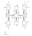
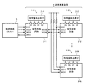
図17は、本実施形態の姿勢演算装置の構成例を示す図である。図17に示すように、本実施形態の姿勢演算装置4は、N個の物理量検出装置1−1〜1−Nを備えている。物理量検出装置1−1〜1−Nは、すべて、上述した本実施形態又は変形例の物理量検出装置1であり、各物理量検出装置1−k(k=1〜N)は、物理量検出素子2−k及び信号処理回路3−kを備えている。
2. Posture Calculation Device FIG. 17 is a diagram illustrating a configuration example of the posture calculation device according to the present embodiment. As illustrated in FIG. 17, the posture calculation device 4 of the present embodiment includes N physical quantity detection devices 1-1 to 1-N. The physical quantity detection devices 1-1 to 1-N are all the physical
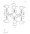
物理量検出装置1−1(「第1の物理量検出装置」の一例)が備えている信号処理回路3−1のMSCK端子と物理量検出装置1−2〜1−N(「第2〜第Nの物理量検出装置」の一例)の各々が備えている信号処理回路3−2〜3−NのSCLK端子とが電気的に接続されている。また、物理量検出装置1−1が備えている信号処理回路3−1のMSDA端子(「第2の端子」の一例)と物理量検出装置1−2〜1−Nの各々が備えている信号処理回路3−2〜3−NのMOSI端子(「第1の端子」の一例)とが電気的に接続されている。そして、物理量検出装置1−1(信号処理回路3−1の姿勢演算部40(図1参照))が姿勢演算を行う。 The MSCK terminal of the signal processing circuit 3-1 included in the physical quantity detection device 1-1 (an example of “first physical quantity detection device”) and the physical quantity detection devices 1-2 to 1-N (“second to Nth The SCLK terminals of the signal processing circuits 3-2 to 3 -N included in each example of the “physical quantity detection device” are electrically connected. Further, the signal processing included in each of the MSDA terminal (an example of “second terminal”) of the signal processing circuit 3-1 included in the physical quantity detection device 1-1 and the physical quantity detection devices 1-2 to 1-N. The MOSI terminals (an example of “first terminal”) of the circuits 3-2 to 3 -N are electrically connected. Then, the physical quantity detection device 1-1 (the posture calculation unit 40 (see FIG. 1) of the signal processing circuit 3-1) performs the posture calculation.
物理量検出装置1−1(信号処理回路3−1)は、第1インターフェース回路70(図1参照)を介して、ホストである制御装置5と通信する。信号処理回路3−1の第1インターフェース回路70は、SPIインターフェース回路として機能し、マスターである制御装置5は、例えば、図7〜図9に示した通信フォーマットに従い、スレーブである物理量検出装置1−1(信号処理回路3−1)に対して、データの書き込みやデータの読み出しを行い、あるいは、コマンドを送信する。
The physical quantity detection device 1-1 (signal processing circuit 3-1) communicates with the
また、物理量検出装置1−1(信号処理回路3−1)は、I2Cインターフェース回路である第2インターフェース回路80(図1参照)を介して、物理量検出装置1−2〜1−Nとそれぞれ通信する。物理量検出装置1−2〜1−Nの各々は、第1インターフェース回路70(図1参照)を介して、物理量検出装置1−1と通信する。信号処理回路3−2〜3−Nの各々において、XCS端子が電源にプルアップされており、第1インターフェース回路70は、I2Cインターフェース回路として機能する。マスターである物理量検出装置1−1(信号処理回路3−1)は、例えば、図10及び図11に示した通信フォーマットに従い、スレーブである物理量検出装置1−2〜1−N(信号処理回路3−2〜3−N)に対して、データの書き込みやデータの読み出しを行う。
Further, the physical quantity detection device 1-1 (signal processing circuit 3-1) is connected to the physical quantity detection devices 1-2 to 1-N via the second interface circuit 80 (see FIG. 1) which is an I 2 C interface circuit. Communicate with each other. Each of the physical quantity detection devices 1-2 to 1-N communicates with the physical quantity detection device 1-1 via the first interface circuit 70 (see FIG. 1). In each of the signal processing circuits 3-2 to 3 -N, the XCS terminal is pulled up to the power source, and the
なお、物理量検出装置1−1から視たとき、制御装置5は、前述の「第1の外部装置」に相当し、物理量検出装置1−2〜1−Nは、前述の「第2の外部装置」〜「第Nの外部装置」に相当する。
When viewed from the physical quantity detection device 1-1, the
制御装置5は、姿勢演算装置4から、第1〜第Nの物理量信号の値(角速度ω1〜ωN)や姿勢の情報(クォータニオンあるいは第1〜第Nの角度等)を取得することができる。
The
例えば、N=3のケースにおいて、物理量検出装置1−1の信号処理回路3−1の記憶部60(レジスター61及び不揮発性メモリー62)が図12〜図15に示したアドレスマップのように構成されている場合、制御装置5が姿勢演算装置4から第1〜第3の物理量信号の値(角速度ω1,ω2,ω3)を所定の周期Δtで取得するための手順は以下のようになる。
For example, in the case of N = 3, the storage unit 60 (the
まず、制御装置5は、図7に示した通信フォーマットに従い、信号処理回路3−1のレジスター61のアドレス0x11のビット2(MCTL[2])とビット1(MCTL[1])にともに1を書き込み、第2インターフェース回路80のマニュアル動作を「読み出し」と「許可」に設定する。
First, in accordance with the communication format shown in FIG. 7, the
また、制御装置5は、図7に示した通信フォーマットに従い、信号処理回路3−1のレジスター61のアドレス0x16のビット7〜0(レジスターMI2CRAD[7:0])に0x0Aを書き込み、信号処理回路3−1の第2インターフェース回路80のマニュアル動作による通信で用いられるレジスターアドレス(図10及び図11のレジスターアドレスMI2CRAD[7:0])を0x0Aに設定する。
Further, the
次に、制御装置5は、周期Δtで、図8に示した通信フォーマットに従い、信号処理回路3−1のレジスター61のアドレス0x0A(レジスターRDGR)から第1の物理量信号(角速度ω1)を読み出して取得する。
Next, the
また、制御装置5は、周期Δtで、図7に示した通信フォーマットに従い、信号処理回路3−1のレジスター61のアドレス0x15のビット6〜0(レジスターMI2CSAD[6:0])に物理量検出装置1−2のスレーブアドレスを書き込んだ後、図9に示した通信フォーマットに従い、当該レジスター61のアドレス0x14(レジスターMI2CST)を指定して、信号処理回路3−1の第2インターフェース回路80のマニュアル動作を開始させるためのコマンドを送信する。これにより、物理量検出装置1−1(信号処理回路3−1)は、周期Δtで、図11に示した通信フォーマットに従い、物理量検出装置1−2(信号処理回路3−2)のレジスター61のアドレス0x0Aから第2の物理量信号(角速度ω2)を読み出して自身のレジスター61のアドレス0x18(レジスターMI2CRD)に記憶する。
Further, the
そして、制御装置5は、周期Δtで、図8に示した通信フォーマットに従い、信号処理回路3−1のレジスター61のアドレス0x18(レジスターRDGR)から第2の物理量信号(角速度ω2)を読み出して取得する。
Then, the
また、制御装置5は、周期Δtで、図7に示した通信フォーマットに従い、信号処理回路3−1のレジスター61のアドレス0x15のビット6〜0(レジスターMI2CSAD[6:0])に物理量検出装置1−3のスレーブアドレスを書き込んだ後、図9に示した通信フォーマットに従い、当該レジスター61のアドレス0x14(レジスターMI2CST)を指定して、信号処理回路3−1の第2インターフェース回路80のマニュアル動作を開始させるためのコマンドを送信する。これにより、物理量検出装置1−1(信号処理回路3−1)は、周期Δtで、図11に示した通信フォーマットに従い、物理量検出装置1−3(信号処理回路3−3)のレジスター61のアドレス0x0Aから第3の物理量信号(角速度ω3)を読み出して自身のレジスター61のアドレス0x18(レジスターMI2CRD)に記憶する。
Further, the
そして、制御装置5は、周期Δtで、図8に示した通信フォーマットに従い、信号処理回路3−1のレジスター61のアドレス0x18(レジスターRDGR)から第3の物理量信号(角速度ω3)を読み出して取得する。
Then, the
また、例えば、N=3のケースにおいて、物理量検出装置1−1の信号処理回路3−1の記憶部60(レジスター61及び不揮発性メモリー62)が図12〜図15に示したアドレスマップのように構成されている場合、制御装置5が姿勢演算装置4から姿勢の情報を所定の周期Δtで取得するための手順は以下のようになる。
Further, for example, in the case of N = 3, the storage unit 60 (the
まず、制御装置5は、図7に示した通信フォーマットに従い、信号処理回路3−1のレジスター61のアドレス0x11のビット0(MCTL[0])に1を書き込み、姿勢演算部40による姿勢演算を許可する。
First, in accordance with the communication format shown in FIG. 7, the
これにより、物理量検出装置1−1(信号処理回路3−1)は、周期Δtで、図11に示した通信フォーマットに従い、物理量検出装置1−2(信号処理回路3−2)のレジスター61のアドレス0x0Aから第2の物理量信号(角速度ω2)を読み出して自身の記憶部60(レジスター61)に記憶する。なお、あらかじめ、信号処理回路3−1の不揮発性メモリー62において、アドレス0x00(メモリーMI2CSA1)には物理量検出装置1−2のスレーブアドレスが記憶され、アドレス0x02(メモリーMI2CRA1)には0x0Aが記憶されており、信号処理回路3−1は、これらの情報を用いて、第2の物理量信号(角速度ω2)を読み出す。
As a result, the physical quantity detection device 1-1 (signal processing circuit 3-1) has a period Δt and follows the communication format shown in FIG. 11 in the
また、物理量検出装置1−1(信号処理回路3−1)は、周期Δtで、図11に示した通信フォーマットに従い、物理量検出装置1−3(信号処理回路3−3)のレジスター61のアドレス0x0Aから第3の物理量信号(角速度ω3)を読み出して自身の記憶部60(レジスター61)に記憶する。なお、あらかじめ、信号処理回路3−1の不揮発性メモリー62において、アドレス0x01(メモリーMI2CSA2)には物理量検出装置1−3のスレーブアドレスが記憶され、アドレス0x03(メモリーMI2CRA2)には0x0Aが記憶されており、信号処理回路3−1は、これらの情報を用いて、第3の物理量信号(角速度ω3)を読み出す。
In addition, the physical quantity detection device 1-1 (signal processing circuit 3-1) has the cycle Δt, and the address of the
そして、信号処理回路3−1の姿勢演算部40は、周期Δtで、検出回路30から第1の物理量信号(角速度ω1)を取得し、また、それぞれ周期Δtで、記憶部60(レジスター61)から第2の物理量信号(角速度ω2)及び第3の物理量信号(角速度ω3)を取得し、姿勢演算を行い、姿勢演算の結果の情報をレジスター61のアドレス0x12(
レジスターRDAR)に記憶する。なお、信号処理回路3−1の姿勢演算部40は、不揮発性メモリー62のアドレス0x04のビット1〜0(AXISCTL[1:0])に応じて、第1〜第3の物理量信号(角速度ω1,ω2,ω3)を3軸角速度ωx,ωy,ωzに変換し、不揮発性メモリー62のアドレス0x04のビット2(AXISCTL[2])の設定に応じて、姿勢演算として角度演算又はクォータニオン演算を行う。
Then, the
Register RDAR). Note that the
次に、制御装置5は、周期Δtで、図8に示した通信フォーマットに従い、信号処理回路3−1のレジスター61のアドレス0x12(レジスターRDAR)から姿勢演算の結果を読み出して取得する。
Next, the
図18に、物理量検出装置1−1(信号処理回路3−1)における姿勢演算のタイムチャートの一例を示す。図18に示すように、物理量検出装置1−1(信号処理回路3−1)において、姿勢演算部40は、第1の物理量信号(角速度ω1)を検出回路30から取得するため、第2インターフェース回路80を介して第1の物理量信号(角速度ω1)を取得する必要がない。そのため、本実施形態の姿勢演算装置4では、姿勢演算の周期Δtは、物理量検出装置1−1(信号処理回路3−1)が、第2インターフェース回路80を介して、物理量検出装置1−2(信号処理回路3−2)及び物理量検出装置1−3(信号処理回路3−3)からそれぞれ第2の物理量信号(角速度ω2)及び第3の物理量信号(角速度ω3)を取得するのに要する通信時間によって決まる。これに対して、従来の姿勢演算システムでは、ホストである制御装置5が、物理量検出装置1−1〜1−3からそれぞれ第1〜第3の物理量信号(角速度ω1,ω2,ω3)を取得して姿勢演算を行うため、姿勢演算の周期Δtは、制御装置5が、物理量検出装置1−1〜1−3(信号処理回路3−2)及び物理量検出装置1−3(信号処理回路3−3)から第1〜第3の物理量信号(角速度ω1,ω2,ω3)を取得するのに要する通信時間よりも短くすることができない。すなわち、本実施形態の姿勢演算装置4は、従来の姿勢演算システムよりも短い周期(高いレート)で姿勢演算を行うことができる。
FIG. 18 shows an example of a time chart of posture calculation in the physical quantity detection device 1-1 (signal processing circuit 3-1). As shown in FIG. 18, in the physical quantity detection device 1-1 (signal processing circuit 3-1), the
以上に説明したように、本実施形態によれば、物理量検出装置1−1が備える信号処理回路3−1が第1の物理量信号を生成し、かつ、MSDA端子を介して、物理量検出装置1−2〜1−Nがそれぞれ備える信号処理回路3−1〜3−NのMOSI端子から出力される第2〜第Nの物理量信号を取得して、姿勢演算を実行する姿勢演算装置4を構成することができる。
As described above, according to this embodiment, the signal processing circuit 3-1 included in the physical quantity detection device 1-1 generates the first physical quantity signal, and the physical
そして、本実施形態の姿勢演算装置4では、物理量検出装置1−1が備える信号処理回路3−1は、外部装置と通信して第1の物理量信号を取得する必要がなく、また、物理量検出装置1−2〜1−Nがそれぞれ備える信号処理回路3−2〜3−Nから第2〜第Nの物理量信号を取得するのと並行して、検出回路30が第1の物理量信号を生成することができるので、第1〜第Nの物理量信号を取得する時間を短くすることができる。その結果、本実施形態の姿勢演算装置4によれば、従来よりも姿勢演算の周期Δtが短くなり、姿勢演算の精度を向上させることができる。
In the posture calculation device 4 of the present embodiment, the signal processing circuit 3-1 included in the physical quantity detection device 1-1 does not need to communicate with an external device to acquire the first physical quantity signal, and the physical quantity detection In parallel with the acquisition of the second to Nth physical quantity signals from the signal processing circuits 3-2 to 3 -N included in the devices 1-2 to 1 -N, the
また、本実施形態の姿勢演算装置4は、同じ構成のN個の物理量検出装置を用いて実現することができるので、開発コストを削減することができる。 Moreover, since the attitude | position calculating apparatus 4 of this embodiment is realizable using N physical quantity detection apparatuses of the same structure, it can reduce development cost.
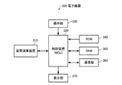
3.電子機器
図19は、本実施形態の電子機器の構成の一例を示す機能ブロック図である。図19に示すように、本実施形態の電子機器300は、姿勢演算装置310、制御装置(MCU)320、操作部330、ROM(Read Only Memory)340、RAM(Random Access Memory)350、通信部360、表示部370を含んで構成されている。なお、本実施形態の電子機器は、図19の構成要素(各部)の一部を省略又は変更し、あるいは、他の構成
要素を付加した構成としてもよい。
3. Electronic Device FIG. 19 is a functional block diagram showing an example of the configuration of the electronic device of the present embodiment. As illustrated in FIG. 19, the electronic apparatus 300 according to the present embodiment includes an
姿勢演算装置310は、第1〜第Nの物理量信号に基づいて姿勢演算を行い、姿勢演算の結果を制御装置(MCU)320に出力する。姿勢演算装置310として、例えば、上述した本実施形態の姿勢演算装置4を適用することができる。
The
制御装置(MCU)320は、ROM340等に記憶されているプログラムに従い、姿勢演算装置310に通信信号を発信し、姿勢演算装置310の出力信号を用いて各種の計算処理や制御処理を行う。その他、制御装置(MCU)320は、操作部330からの操作信号に応じた各種の処理、外部装置とデータ通信を行うために通信部360を制御する処理、表示部370に各種の情報を表示させるための表示信号を送信する処理等を行う。
The control unit (MCU) 320 transmits a communication signal to the
操作部330は、操作キーやボタンスイッチ等により構成される入力装置であり、ユーザーによる操作に応じた操作信号を制御装置(MCU)320に出力する。
The
ROM340は、制御装置(MCU)320が各種の計算処理や制御処理を行うためのプログラムやデータ等を記憶している。
The
RAM350は、制御装置(MCU)320の作業領域として用いられ、ROM340から読み出されたプログラムやデータ、操作部330から入力されたデータ、制御装置(MCU)320が各種プログラムに従って実行した演算結果等を一時的に記憶する。
The
通信部360は、制御装置(MCU)320と外部装置との間のデータ通信を成立させるための各種制御を行う。
The
表示部370は、LCD(Liquid Crystal Display)等により構成される表示装置であり、CPU320から入力される表示信号に基づいて各種の情報を表示する。表示部370には操作部330として機能するタッチパネルが設けられていてもよい。
The
姿勢演算装置310として、例えば上述した本実施形態の姿勢演算装置4を適用することにより、姿勢演算の精度を向上させることができるので、信頼性の高い電子機器を実現することができる。
For example, by applying the posture calculation device 4 of the present embodiment described above as the
このような電子機器300としては種々の電子機器が考えられ、例えば、パーソナルコンピューター(例えば、モバイル型パーソナルコンピューター、ラップトップ型パーソナルコンピューター、タブレット型パーソナルコンピューター)、スマートフォンや携帯電話機などの移動体端末、デジタルカメラ、インクジェット式吐出装置(例えば、インクジェットプリンター)、ルーターやスイッチなどのストレージエリアネットワーク機器、ローカルエリアネットワーク機器、移動体端末基地局用機器、テレビ、ビデオカメラ、ビデオレコーダー、カーナビゲーション装置、リアルタイムクロック装置、ページャー、電子手帳(通信機能付も含む)、電子辞書、電卓、電子ゲーム機器、ゲーム用コントローラー、ワードプロセッサー、ワークステーション、テレビ電話、防犯用テレビモニター、電子双眼鏡、POS端末、医療機器(例えば電子体温計、血圧計、血糖計、心電図計測装置、超音波診断装置、電子内視鏡)、魚群探知機、各種測定機器、計器類(例えば、車両、航空機、船舶の計器類)、フライトシミュレーター、ヘッドマウントディスプレイ、モーショントレース、モーショントラッキング、モーションコントローラー、PDR(歩行者位置方位計測)等が挙げられる。 Various electronic devices can be considered as such an electronic device 300, for example, a personal computer (for example, a mobile personal computer, a laptop personal computer, a tablet personal computer), a mobile terminal such as a smartphone or a mobile phone, Digital cameras, inkjet discharge devices (for example, inkjet printers), storage area network devices such as routers and switches, local area network devices, mobile terminal base station devices, televisions, video cameras, video recorders, car navigation devices, real time Clock devices, pagers, electronic notebooks (including those with communication functions), electronic dictionaries, calculators, electronic game machines, game controllers, word processors, work Station, video phone, crime prevention TV monitor, electronic binoculars, POS terminal, medical equipment (eg, electronic thermometer, blood pressure monitor, blood glucose meter, electrocardiogram measuring device, ultrasonic diagnostic device, electronic endoscope), fish detector, various measurements Examples of such devices include instruments, instruments (for example, vehicles, aircraft, and ship instruments), flight simulators, head mounted displays, motion traces, motion tracking, motion controllers, and PDR (pedestrian orientation measurement).
図20は、本実施形態の電子機器300の一例であるデジタルカメラ1300を模式的に示す斜視図である。なお、図20には、外部機器との接続についても簡易的に示してい
る。ここで、通常のカメラは、被写体の光像により銀塩写真フィルムを感光するのに対し、デジタルカメラ1300は、被写体の光像をCCD(Charge Coupled Device)などの撮像素子により光電変換して撮像信号(画像信号)を生成する。
FIG. 20 is a perspective view schematically showing a
デジタルカメラ1300におけるケース(ボディー)1302の背面には、表示部1310が設けられ、CCDによる撮像信号に基づいて表示を行う構成になっており、表示部1310は、被写体を電子画像として表示するファインダーとして機能する。また、ケース1302の正面側(図中裏面側)には、光学レンズ(撮像光学系)やCCDなどを含む受光ユニット1304が設けられている。撮影者が表示部1310に表示された被写体像を確認し、シャッターボタン1306を押下すると、その時点におけるCCDの撮像信号が、メモリー1308に転送・格納される。また、このデジタルカメラ1300においては、ケース1302の側面に、ビデオ信号出力端子1312と、データ通信用の入出力端子1314とが設けられている。そして、ビデオ信号出力端子1312には、テレビモニター1430が、データ通信用の入出力端子1314には、パーソナルコンピューター1440が、それぞれ必要に応じて接続される。さらに、所定の操作により、メモリー1308に格納された撮像信号が、テレビモニター1430や、パーソナルコンピューター1440に出力される構成になっている。デジタルカメラ1300は、姿勢演算装置310を有し、姿勢演算装置310の出力信号を用いて、例えば手振れ補正等の処理を行う。
A
4.移動体
図21は、本実施形態の移動体の一例を示す図(上面図)である。図21に示す移動体400は、姿勢演算装置410、コントローラー440,450,460、バッテリー470、ナビゲーション装置480を含んで構成されている。なお、本実施形態の移動体は、図21の構成要素(各部)の一部を省略し、あるいは、他の構成要素を付加した構成としてもよい。
4). FIG. 21 is a diagram (top view) illustrating an example of the moving object according to the present embodiment. A moving
姿勢演算装置410、コントローラー440,450,460、ナビゲーション装置480は、バッテリー470から供給される電源電圧で動作する。
姿勢演算装置410は、第1〜第Nの物理量信号に基づいて姿勢演算を行い、姿勢演算の結果をコントローラー440,450,460に出力する。
The
コントローラー440,450,460は、それぞれ、姿勢演算装置410の出力信号を用いて、姿勢制御システム、横転防止システム、ブレーキシステム等の各種の制御を行う制御装置である。
The
ナビゲーション装置480は、内蔵のGPS受信機(不図示)の出力情報に基づき、移動体400の位置や時刻その他の各種の情報をディスプレイに表示する。また、ナビゲーション装置480は、GPSの電波が届かない時でも姿勢演算装置410の出力信号に基づいて移動体400の位置や向きを特定し、必要な情報の表示を継続する。
The navigation device 480 displays the position, time, and other various information of the
例えば、姿勢演算装置410として、上述した各実施形態の姿勢演算装置4を適用することにより、姿勢演算の精度を向上させることができるので、信頼性の高い移動体を実現することができる。
For example, by applying the posture calculation device 4 of each of the above-described embodiments as the
このような移動体400としては種々の移動体が考えられ、例えば、自動車(電気自動車も含む)、ジェット機やヘリコプター等の航空機、船舶、ロケット、人工衛星等が挙げられる。
As such a moving
本発明は本実施形態に限定されず、本発明の要旨の範囲内で種々の変形実施が可能であ
る。
The present invention is not limited to the present embodiment, and various modifications can be made within the scope of the gist of the present invention.
例えば、上述した実施形態では、角速度を検出する物理量検出素子を含む物理量検出装置(角速度検出装置)並びに当該物理量検出装置(角速度検出装置)を備えた姿勢演算装置、電子機器及び移動体を例に挙げて説明したが、本発明は、種々の物理量を検出する物理量検出素子を含む物理量検出装置並びに当該物理量検出装置を備えた姿勢演算装置、電子機器及び移動体にも適用することができる。物理量検出素子が検出する物理量は、角速度に限らず、角加速度、加速度、地磁気、傾斜などであってもよい。また、物理量検出素子の振動片は、ダブルT型でなくてもよく、例えば、音叉型やくし歯型であってもよいし、三角柱、四角柱、円柱状等の形状の音片型であってもよい。また、物理量検出素子の振動片の材料としては、水晶(SiO2)の代わりに、例えば、タンタル酸リチウム(LiTaO3)、ニオブ酸リチウム(LiNbO3)等の圧電単結晶やジルコン酸チタン酸鉛(PZT)等の圧電セラミックスなどの圧電性材料を用いてもよいし、シリコン半導体を用いてもよい。また、例えば、シリコン半導体の表面の一部に、駆動電極に挟まれた酸化亜鉛(ZnO)、窒化アルミニウム(AlN)等の圧電薄膜を配置した構造であってもよい。また、物理量検出素子は、圧電型の素子に限らず、動電型、静電容量型、渦電流型、光学型、ひずみゲージ型等の振動式の素子であってもよい。あるいは、物理量検出素子の方式は、振動式に限らず、例えば、光学式、回転式、流体式であってもよい。 For example, in the above-described embodiments, a physical quantity detection device (angular velocity detection device) including a physical quantity detection element that detects an angular velocity, and an attitude calculation device, an electronic apparatus, and a moving body including the physical quantity detection device (angular velocity detection device) are taken as examples. As described above, the present invention can also be applied to a physical quantity detection device including a physical quantity detection element that detects various physical quantities, an attitude calculation device including the physical quantity detection device, an electronic apparatus, and a moving body. The physical quantity detected by the physical quantity detection element is not limited to angular velocity, but may be angular acceleration, acceleration, geomagnetism, inclination, or the like. Further, the vibration piece of the physical quantity detection element may not be a double T type, for example, a tuning fork type or a comb-teeth type, or a sound piece type having a triangular prism shape, a quadrangular prism shape, a cylindrical shape, or the like. Also good. Moreover, as a material of the resonator element of the physical quantity detection element, for example, a piezoelectric single crystal such as lithium tantalate (LiTaO 3 ) or lithium niobate (LiNbO 3 ) or lead zirconate titanate instead of quartz (SiO 2 ). A piezoelectric material such as a piezoelectric ceramic such as (PZT) may be used, or a silicon semiconductor may be used. Further, for example, a structure in which a piezoelectric thin film such as zinc oxide (ZnO) or aluminum nitride (AlN) sandwiched between drive electrodes is arranged on a part of the surface of a silicon semiconductor may be used. The physical quantity detection element is not limited to a piezoelectric element, and may be a vibration element such as an electrodynamic type, a capacitance type, an eddy current type, an optical type, and a strain gauge type. Alternatively, the method of the physical quantity detection element is not limited to the vibration type, and may be, for example, an optical type, a rotary type, or a fluid type.
上述した実施形態および変形例は一例であって、これらに限定されるわけではない。例えば、各実施形態および各変形例を適宜組み合わせることも可能である。 The above-described embodiments and modifications are merely examples, and the present invention is not limited to these. For example, it is possible to appropriately combine each embodiment and each modification.
本発明は、実施の形態で説明した構成と実質的に同一の構成(例えば、機能、方法及び結果が同一の構成、あるいは目的及び効果が同一の構成)を含む。また、本発明は、実施の形態で説明した構成の本質的でない部分を置き換えた構成を含む。また、本発明は、実施の形態で説明した構成と同一の作用効果を奏する構成又は同一の目的を達成することができる構成を含む。また、本発明は、実施の形態で説明した構成に公知技術を付加した構成を含む。 The present invention includes configurations that are substantially the same as the configurations described in the embodiments (for example, configurations that have the same functions, methods, and results, or configurations that have the same objects and effects). In addition, the invention includes a configuration in which a non-essential part of the configuration described in the embodiment is replaced. In addition, the present invention includes a configuration that exhibits the same operational effects as the configuration described in the embodiment or a configuration that can achieve the same object. Further, the invention includes a configuration in which a known technique is added to the configuration described in the embodiment.
1…物理量検出装置、2…物理量検出素子、3…信号処理回路、4…姿勢演算装置、5…制御装置、10…基準電圧回路、20…駆動回路、21…I/V変換回路、22…ローパスフィルター、23…ハイパスフィルター、24…コンパレーター、25…全波整流回路、26…積分器、27…コンパレーター、28…コンパレーター、30…検出回路、31…QVアンプ、32…可変ゲインアンプ、33…同期検波回路、34…A/D変換回路、35…DSP、40…姿勢演算部、41A,41B,41C…Dフリップフロップ、42…NOT回路、43…NOR回路、44…カウンター、45A,45B…乗算器、46…変換部、47…行列演算部、48…加算器、49…正規化部、50…クロック生成回路、60…記憶部、61…レジスター、62…不揮発性メモリー、70…第1インターフェース回路、80…第2インターフェース回路、90…補正処理部、101a,101b…駆動振動腕、102…検出振動腕、103…錘部、104a,104b…駆動用基部、105a,105b…連結腕、106…錘部、107…検出用基部、112,113…駆動電極、114,115…検出電極、116…共通電極、300…電子機器、310…姿勢演算装置、312…駆動回路、320…制御装置(MCU)、330…操作部、340…ROM、350…RAM、360…通信部、370…表示部、400…移動体、410…姿勢演算装置、440,450,460…コントローラー、470…バッテリー、480…ナビゲーション装置、1300…デジタルカメラ、1302…ケース、1304…受光ユニット、1306…シャッターボタン、1308…メモリー、1310…表示部、1312…ビデオ信号出力端子、1314…入出力端子、1430…テレビモニター、1440…パーソナルコンピューター
DESCRIPTION OF
Claims (12)
前記第1の物理量信号を出力可能な第1の端子と、
第2〜第N(N≧2)の物理量信号を入力可能な第2の端子と、
前記第1〜第Nの物理量信号に基づいて姿勢演算を実行可能な姿勢演算部と、を含む、信号処理回路。 A detection circuit that generates a first physical quantity signal based on an output signal of the physical quantity detection element;
A first terminal capable of outputting the first physical quantity signal;
A second terminal capable of inputting second to Nth (N ≧ 2) physical quantity signals;
A posture calculation unit capable of performing posture calculation based on the first to Nth physical quantity signals.
前記姿勢演算部は、前記駆動信号に基づくクロック信号を用いて前記姿勢演算を行う、請求項1乃至4のいずれか1項に記載の信号処理回路。 A drive circuit for generating a drive signal for driving the physical quantity detection element;
The signal processing circuit according to claim 1, wherein the attitude calculation unit performs the attitude calculation using a clock signal based on the drive signal.
前記姿勢演算部は、前記設定情報を用いて前記姿勢演算を行う、請求項1乃至5のいずれか1項に記載の信号処理回路。 A storage unit that stores setting information of correspondence between the first to Nth physical quantity signals and the first to Nth detection axes;
The signal processing circuit according to claim 1, wherein the posture calculation unit performs the posture calculation using the setting information.
第1の前記物理量検出装置が備えている前記信号処理回路の前記第2の端子と、第2〜第Nの前記物理量検出装置の各々が備えている前記信号処理回路の前記第1の端子とが電気的に接続され、
前記第1の前記物理量検出装置が備えている前記信号処理回路の前記姿勢演算部が前記姿勢演算を行う、姿勢演算装置。 N physical quantity detection devices according to claim 9 are provided,
The second terminal of the signal processing circuit provided in the first physical quantity detection device, and the first terminal of the signal processing circuit provided in each of the second to Nth physical quantity detection devices Are electrically connected,
An attitude calculation device in which the attitude calculation unit of the signal processing circuit included in the first physical quantity detection device performs the attitude calculation.
Priority Applications (1)
| Application Number | Priority Date | Filing Date | Title |
|---|---|---|---|
| JP2016125419A JP6808997B2 (en) | 2016-06-24 | 2016-06-24 | Signal processing circuit, physical quantity detection device, attitude calculation device, electronic device and mobile body |
Applications Claiming Priority (1)
| Application Number | Priority Date | Filing Date | Title |
|---|---|---|---|
| JP2016125419A JP6808997B2 (en) | 2016-06-24 | 2016-06-24 | Signal processing circuit, physical quantity detection device, attitude calculation device, electronic device and mobile body |
Publications (2)
| Publication Number | Publication Date |
|---|---|
| JP2017227591A true JP2017227591A (en) | 2017-12-28 |
| JP6808997B2 JP6808997B2 (en) | 2021-01-06 |
Family
ID=60889173
Family Applications (1)
| Application Number | Title | Priority Date | Filing Date |
|---|---|---|---|
| JP2016125419A Active JP6808997B2 (en) | 2016-06-24 | 2016-06-24 | Signal processing circuit, physical quantity detection device, attitude calculation device, electronic device and mobile body |
Country Status (1)
| Country | Link |
|---|---|
| JP (1) | JP6808997B2 (en) |
Cited By (4)
| Publication number | Priority date | Publication date | Assignee | Title |
|---|---|---|---|---|
| US20140324392A1 (en) * | 2013-04-24 | 2014-10-30 | Seiko Epson Corporation | Physical quantity detection circuit, physical quantity detector, electronic apparatus and moving object |
| CN113227709A (en) * | 2018-12-20 | 2021-08-06 | 罗伯特·博世有限公司 | System with micromechanical clock generation system component |
| CN113741262A (en) * | 2021-08-27 | 2021-12-03 | 天津新松智能科技有限公司 | Ship control system |
| WO2023026470A1 (en) * | 2021-08-27 | 2023-03-02 | 国立大学法人東北大学 | Magnetic field sensor and magnetic field detection method |
Citations (6)
| Publication number | Priority date | Publication date | Assignee | Title |
|---|---|---|---|---|
| JP2007183138A (en) * | 2006-01-05 | 2007-07-19 | Kenzo Nonami | Compact attitude sensor |
| JP2011503522A (en) * | 2007-07-06 | 2011-01-27 | インベンセンス インコーポレイテッド | Integrated motion processing unit (MPU) with MEMS inertial sensing and built-in digital electronics |
| JP2014190900A (en) * | 2013-03-28 | 2014-10-06 | Seiko Epson Corp | Position calculation method and position calculation apparatus |
| JP2014211350A (en) * | 2013-04-18 | 2014-11-13 | セイコーエプソン株式会社 | Electronic device, integrated circuit, electronic apparatus, and mobile body |
| JP2015184181A (en) * | 2014-03-25 | 2015-10-22 | セイコーエプソン株式会社 | Physical quantity detection circuit, physical quantity detection device, electronic apparatus, and mobile entity |
| JP2015184158A (en) * | 2014-03-25 | 2015-10-22 | セイコーエプソン株式会社 | Error estimation method, motion analysis method, error estimation device, and program |
-
2016
- 2016-06-24 JP JP2016125419A patent/JP6808997B2/en active Active
Patent Citations (6)
| Publication number | Priority date | Publication date | Assignee | Title |
|---|---|---|---|---|
| JP2007183138A (en) * | 2006-01-05 | 2007-07-19 | Kenzo Nonami | Compact attitude sensor |
| JP2011503522A (en) * | 2007-07-06 | 2011-01-27 | インベンセンス インコーポレイテッド | Integrated motion processing unit (MPU) with MEMS inertial sensing and built-in digital electronics |
| JP2014190900A (en) * | 2013-03-28 | 2014-10-06 | Seiko Epson Corp | Position calculation method and position calculation apparatus |
| JP2014211350A (en) * | 2013-04-18 | 2014-11-13 | セイコーエプソン株式会社 | Electronic device, integrated circuit, electronic apparatus, and mobile body |
| JP2015184181A (en) * | 2014-03-25 | 2015-10-22 | セイコーエプソン株式会社 | Physical quantity detection circuit, physical quantity detection device, electronic apparatus, and mobile entity |
| JP2015184158A (en) * | 2014-03-25 | 2015-10-22 | セイコーエプソン株式会社 | Error estimation method, motion analysis method, error estimation device, and program |
Cited By (8)
| Publication number | Priority date | Publication date | Assignee | Title |
|---|---|---|---|---|
| US20140324392A1 (en) * | 2013-04-24 | 2014-10-30 | Seiko Epson Corporation | Physical quantity detection circuit, physical quantity detector, electronic apparatus and moving object |
| US10545165B2 (en) * | 2013-04-24 | 2020-01-28 | Seiko Epson Corporation | Physical quantity detection circuit, physical quantity detector, electronic apparatus and moving object |
| CN113227709A (en) * | 2018-12-20 | 2021-08-06 | 罗伯特·博世有限公司 | System with micromechanical clock generation system component |
| JP2022513504A (en) * | 2018-12-20 | 2022-02-08 | ロベルト・ボッシュ・ゲゼルシャフト・ミト・ベシュレンクテル・ハフツング | System with micromechanical clocking system components |
| JP7212782B2 (en) | 2018-12-20 | 2023-01-25 | ロベルト・ボッシュ・ゲゼルシャフト・ミト・ベシュレンクテル・ハフツング | Systems with micromechanical clocking system components |
| US11959747B2 (en) | 2018-12-20 | 2024-04-16 | Robert Bosch Gmbh | Micromechanical clocking system with improved timing precision |
| CN113741262A (en) * | 2021-08-27 | 2021-12-03 | 天津新松智能科技有限公司 | Ship control system |
| WO2023026470A1 (en) * | 2021-08-27 | 2023-03-02 | 国立大学法人東北大学 | Magnetic field sensor and magnetic field detection method |
Also Published As
| Publication number | Publication date |
|---|---|
| JP6808997B2 (en) | 2021-01-06 |
Similar Documents
| Publication | Publication Date | Title |
|---|---|---|
| JP6834581B2 (en) | Physical quantity sensors, electronic devices and mobile objects | |
| JP6222426B2 (en) | Physical quantity detection circuit, physical quantity detection device, electronic device, and moving object | |
| JP6828544B2 (en) | Failure diagnosis method for sensor element control device, physical quantity sensor, electronic device, mobile body and physical quantity sensor | |
| US10116275B2 (en) | Physical quantity detection circuit, physical quantity detection device, electronic apparatus, and vehicle | |
| JP6808997B2 (en) | Signal processing circuit, physical quantity detection device, attitude calculation device, electronic device and mobile body | |
| JP7151061B2 (en) | FAILURE DETERMINATION CIRCUIT, PHYSICAL QUALITY DETECTION DEVICE, ELECTRONIC DEVICE, MOBILE OBJECT, AND FAILURE DETERMINATION METHOD | |
| JP2016178601A (en) | Data processing circuit, circuit for physical quantity detection, physical quantity detection device, electronic equipment, and mobile body | |
| JP2018165641A (en) | Failure determination circuit, physical quantity detection device, electronic apparatus, and movable body | |
| JP2021185356A (en) | Physical quantity detection circuit, physical quantity detection device, electronic apparatus and moving body | |
| JP7234655B2 (en) | Physical quantity detection circuit, physical quantity sensor, electronic device, moving object, and operation method of physical quantity detection circuit | |
| JP7447571B2 (en) | Physical quantity detection circuit, physical quantity sensor, electronic equipment, moving object, and operation method of physical quantity detection circuit | |
| JP6586735B2 (en) | Circuit device, physical quantity detection device, electronic device, and moving object | |
| US20230332891A1 (en) | Physical Quantity Detection Circuit, Physical Quantity Sensor, Electronic Instrument, Vehicle, And Method For Diagnosing Failure Of Physical Quantity Sensor | |
| JP2018189413A (en) | Inertia sensor element control device, inertia sensor, electronic apparatus, moving body and temperature compensation information update method for inertial sensor element control device | |
| JP7456284B2 (en) | PHYSICAL QUANTITY DETECTION CIRCUIT, PHYSICAL QUANTITY DETECTION DEV | |
| JP6465294B2 (en) | Drive circuit, vibration device, electronic device, and moving object | |
| JP6492739B2 (en) | Circuit device, physical quantity detection device, electronic device, and moving object | |
| JP7322718B2 (en) | Physical quantity detection circuit, physical quantity sensor, electronic device, moving object, and operation method of physical quantity detection circuit | |
| JP6780467B2 (en) | Physical quantity sensors, electronic devices and mobile objects | |
| JP6521236B2 (en) | Physical quantity processing circuit, physical quantity processing device, electronic device and moving body | |
| JP7323015B2 (en) | Physical quantity processing circuit, physical quantity detection device, electronic device, and moving object | |
| JP6756175B2 (en) | Rectifier circuit, drive circuit, physical quantity detector, electronic device and moving object | |
| JP6478034B2 (en) | Angular velocity detection device evaluation method, signal processing circuit, angular velocity detection device, electronic apparatus, and moving body | |
| JP6641874B2 (en) | Physical quantity detection device, electronic equipment and moving object |
Legal Events
| Date | Code | Title | Description |
|---|---|---|---|
| A621 | Written request for application examination |
Free format text: JAPANESE INTERMEDIATE CODE: A621 Effective date: 20190411 |
|
| A977 | Report on retrieval |
Free format text: JAPANESE INTERMEDIATE CODE: A971007 Effective date: 20200324 |
|
| A131 | Notification of reasons for refusal |
Free format text: JAPANESE INTERMEDIATE CODE: A131 Effective date: 20200331 |
|
| A521 | Request for written amendment filed |
Free format text: JAPANESE INTERMEDIATE CODE: A523 Effective date: 20200525 |
|
| TRDD | Decision of grant or rejection written | ||
| A01 | Written decision to grant a patent or to grant a registration (utility model) |
Free format text: JAPANESE INTERMEDIATE CODE: A01 Effective date: 20201110 |
|
| A61 | First payment of annual fees (during grant procedure) |
Free format text: JAPANESE INTERMEDIATE CODE: A61 Effective date: 20201123 |
|
| R150 | Certificate of patent or registration of utility model |
Ref document number: 6808997 Country of ref document: JP Free format text: JAPANESE INTERMEDIATE CODE: R150 |