JP2017223874A - Image forming apparatus - Google Patents
Image forming apparatus Download PDFInfo
- Publication number
- JP2017223874A JP2017223874A JP2016120233A JP2016120233A JP2017223874A JP 2017223874 A JP2017223874 A JP 2017223874A JP 2016120233 A JP2016120233 A JP 2016120233A JP 2016120233 A JP2016120233 A JP 2016120233A JP 2017223874 A JP2017223874 A JP 2017223874A
- Authority
- JP
- Japan
- Prior art keywords
- charging
- bias
- forming apparatus
- image forming
- transfer
- Prior art date
- Legal status (The legal status is an assumption and is not a legal conclusion. Google has not performed a legal analysis and makes no representation as to the accuracy of the status listed.)
- Withdrawn
Links
Images


Classifications
-
- G—PHYSICS
- G03—PHOTOGRAPHY; CINEMATOGRAPHY; ANALOGOUS TECHNIQUES USING WAVES OTHER THAN OPTICAL WAVES; ELECTROGRAPHY; HOLOGRAPHY
- G03G—ELECTROGRAPHY; ELECTROPHOTOGRAPHY; MAGNETOGRAPHY
- G03G15/00—Apparatus for electrographic processes using a charge pattern
- G03G15/50—Machine control of apparatus for electrographic processes using a charge pattern, e.g. regulating differents parts of the machine, multimode copiers, microprocessor control
-
- G—PHYSICS
- G03—PHOTOGRAPHY; CINEMATOGRAPHY; ANALOGOUS TECHNIQUES USING WAVES OTHER THAN OPTICAL WAVES; ELECTROGRAPHY; HOLOGRAPHY
- G03G—ELECTROGRAPHY; ELECTROPHOTOGRAPHY; MAGNETOGRAPHY
- G03G15/00—Apparatus for electrographic processes using a charge pattern
- G03G15/02—Apparatus for electrographic processes using a charge pattern for laying down a uniform charge, e.g. for sensitising; Corona discharge devices
- G03G15/0266—Arrangements for controlling the amount of charge
-
- G—PHYSICS
- G03—PHOTOGRAPHY; CINEMATOGRAPHY; ANALOGOUS TECHNIQUES USING WAVES OTHER THAN OPTICAL WAVES; ELECTROGRAPHY; HOLOGRAPHY
- G03G—ELECTROGRAPHY; ELECTROPHOTOGRAPHY; MAGNETOGRAPHY
- G03G15/00—Apparatus for electrographic processes using a charge pattern
- G03G15/14—Apparatus for electrographic processes using a charge pattern for transferring a pattern to a second base
- G03G15/16—Apparatus for electrographic processes using a charge pattern for transferring a pattern to a second base of a toner pattern, e.g. a powder pattern, e.g. magnetic transfer
- G03G15/1665—Apparatus for electrographic processes using a charge pattern for transferring a pattern to a second base of a toner pattern, e.g. a powder pattern, e.g. magnetic transfer by introducing the second base in the nip formed by the recording member and at least one transfer member, e.g. in combination with bias or heat
- G03G15/167—Apparatus for electrographic processes using a charge pattern for transferring a pattern to a second base of a toner pattern, e.g. a powder pattern, e.g. magnetic transfer by introducing the second base in the nip formed by the recording member and at least one transfer member, e.g. in combination with bias or heat at least one of the recording member or the transfer member being rotatable during the transfer
- G03G15/1675—Apparatus for electrographic processes using a charge pattern for transferring a pattern to a second base of a toner pattern, e.g. a powder pattern, e.g. magnetic transfer by introducing the second base in the nip formed by the recording member and at least one transfer member, e.g. in combination with bias or heat at least one of the recording member or the transfer member being rotatable during the transfer with means for controlling the bias applied in the transfer nip
Abstract
Description
本発明は、電子写真方式や静電記録方式等により記録材に画像を形成する画像形成装置に関する。 The present invention relates to an image forming apparatus that forms an image on a recording material by an electrophotographic method or an electrostatic recording method.
従来、電子写真方式の画像形成装置は、複写機、プリンタ、プロッタ、ファクシミリ、及びこれらの複数の機能を有する複合機等として広く応用されている。この種の画像形成装置では、感光ドラムの表面を一様に帯電し、その帯電した表面を画像データに応じてレーザ光等によって露光走査して静電潜像を形成する。その静電潜像をトナーによって現像し、その感光ドラム上のトナー像を、転写紙等のシート(記録媒体)上に直接転写するか、あるいは一旦中間転写体上に転写した後、シート上に二次転写する。そのシートを定着装置に通して、転写されたトナー像を定着させて排出する。 2. Description of the Related Art Conventionally, an electrophotographic image forming apparatus has been widely applied as a copying machine, a printer, a plotter, a facsimile, and a multifunction machine having a plurality of these functions. In this type of image forming apparatus, the surface of the photosensitive drum is uniformly charged, and the charged surface is exposed and scanned with a laser beam or the like according to image data to form an electrostatic latent image. The electrostatic latent image is developed with toner, and the toner image on the photosensitive drum is directly transferred onto a sheet (recording medium) such as transfer paper, or once transferred onto an intermediate transfer member and then onto the sheet. Secondary transfer. The sheet is passed through a fixing device, and the transferred toner image is fixed and discharged.
画像形成装置を利用するユーザがコピーボタンを押下してから、1枚目のシートが排出されるまでの時間はFCOT(First Copy Output Time)と呼ばれ、ユーザにとっては待ち時間となるためこの時間を短縮することが望まれている。FCOTの短縮化は画像形成動作における作像部の印刷準備時間を短くすることにより可能であるため、この作像部における印刷準備時間を極力短時間にすることが求められている。 The time from when the user who uses the image forming apparatus presses the copy button until the first sheet is ejected is called FCOT (First Copy Output Time), and this time is a waiting time for the user. It is desired to shorten the length. Since the FCOT can be shortened by shortening the print preparation time of the image forming unit in the image forming operation, it is required to make the print preparation time in the image forming unit as short as possible.
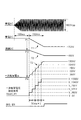
ここで、このような電子写真方式の画像形成装置における帯電位置P1、露光位置P2、現像位置P3、転写位置P4とその各タイミングとについて、図2を参照して説明する。図2に示すように、矢印R1方向に回転する感光ドラムの周囲に、帯電ローラ、現像装置、一次転写ローラが配置されている。そして、感光ドラムの表面を帯電ローラによって帯電させる位置を帯電位置P1、レーザ光Lで露光して静電潜像を形成する位置を露光位置P2とする。露光位置P2で形成された静電潜像を現像装置の現像スリーブがトナーによって現像する位置を現像位置P3、そのトナー像を一次転写ローラによって、被転写材である中間転写ベルトに転写する位置を転写位置P4とする。 Here, the charging position P1, the exposure position P2, the development position P3, the transfer position P4 and their respective timings in such an electrophotographic image forming apparatus will be described with reference to FIG. As shown in FIG. 2, a charging roller, a developing device, and a primary transfer roller are disposed around a photosensitive drum that rotates in the direction of arrow R1. A position where the surface of the photosensitive drum is charged by the charging roller is defined as a charging position P1, and a position where the electrostatic latent image is formed by exposure with the laser beam L is defined as an exposure position P2. The position at which the developing sleeve of the developing device develops the electrostatic latent image formed at the exposure position P2 with toner is the development position P3, and the position at which the toner image is transferred to the intermediate transfer belt, which is the transfer material, by the primary transfer roller. The transfer position is P4.
感光ドラムの表面は、帯電高圧により負電位に帯電される。一次転写ローラには、トナーを中間転写ベルトに転写するために正電位が印加されている。転写位置P4では感光ドラムの表面と一次転写ローラとの電位差により放電が発生するが、感光ドラムの表面の負電位の帯電が不十分な状態で一次転写高圧を印加すると感光ドラムの表面がポジ帯電してしまう。ポジ帯電した感光ドラムの表面は次に帯電高圧により負電位に帯電させようとしても十分な帯電をできず、帯電電位がムラになり、現像した画像に濃度段差が生じて、画像に帯状の縞(以下、横スジという)が現れるという問題があった。 The surface of the photosensitive drum is charged to a negative potential by a charging high voltage. A positive potential is applied to the primary transfer roller in order to transfer the toner to the intermediate transfer belt. At the transfer position P4, a discharge occurs due to the potential difference between the surface of the photosensitive drum and the primary transfer roller. However, when the primary transfer high voltage is applied while the negative potential of the surface of the photosensitive drum is insufficient, the surface of the photosensitive drum is positively charged. Resulting in. Even if the surface of the positively charged photosensitive drum is next charged to a negative potential by charging high voltage, it cannot be sufficiently charged, the charging potential becomes uneven, a density step occurs in the developed image, and the striped stripes appear on the image. (Hereinafter referred to as horizontal stripes).
これを解決するために、従来の画像形成装置においては、画像形成動作開始時に帯電高圧出力が所望の電圧になった後に一次転写高圧を出力し、感光ドラムの表面の帯電電位に段差が発生しないようにしていた。しかしながら、従来の画像形成装置では、帯電高圧出力開始から作像開始までに時間を要し、FCOTが長くなってしまうという問題があった。このような問題を解決するために、一次転写高圧出力タイミングを感光ドラムの帯電高圧出力位置に合わせるように設定する画像形成装置が知られている(特許文献1参照)。この画像形成装置では、転写高圧出力の立ち上がり時にオーバーシュートが発生することを防止する制御が行われており、オーバーシュート時間に相当する局所的な領域で転写バイアスの履歴による横スジが発生することを防止している。 In order to solve this problem, the conventional image forming apparatus outputs the primary transfer high voltage after the charging high voltage output becomes a desired voltage at the start of the image forming operation, and no step occurs in the charging potential on the surface of the photosensitive drum. It was like that. However, the conventional image forming apparatus has a problem that it takes time from the start of charging high-voltage output to the start of image formation, and the FCOT becomes long. In order to solve such a problem, an image forming apparatus is known in which the primary transfer high-voltage output timing is set so as to match the charging high-voltage output position of the photosensitive drum (see Patent Document 1). In this image forming apparatus, control is performed to prevent the occurrence of overshoot when the transfer high-voltage output rises, and horizontal streaks due to transfer bias history occur in a local region corresponding to the overshoot time. Is preventing.
ところで、一次転写ローラは使用環境や耐久等の条件の違いによりそのインピーダンスにばらつきが発生するため、一次転写高圧出力の立ち上がり時間が大きく異なることがある。また、帯電ローラに関しても使用環境や耐久等の条件の違いによりそのインピーダンスにばらつきが発生し、帯電高圧出力の立ち上がり時間が大きく異なることがある。 By the way, since the impedance of the primary transfer roller varies depending on conditions such as the use environment and durability, the rise time of the primary transfer high-voltage output may vary greatly. In addition, the charging roller may vary in impedance due to differences in conditions such as usage environment and durability, and the rising time of the charging high voltage output may vary greatly.
これに対し、上述した特許文献1の画像形成装置では、一次転写ローラ及び帯電ローラのインピーダンスのばらつきに起因する一次転写高圧出力及び帯電高圧出力の立ち上がり時間の変動を考慮したものではなかった。このため、この画像形成装置では、例えば、帯電高圧出力の立ち上がりが遅く、一次転写高圧出力の立ち上がりが速い場合、感光ドラムの表面の負電位の帯電が不十分な状態で一次転写高圧を印加することになり、感光ドラムの表面がポジ帯電してしまう。これにより、ポジ帯電した感光ドラムの表面は、次に帯電高圧により負電位に帯電させようとしても十分な帯電をできず、帯電電位がムラになり、現像した画像に濃度段差が生じて、画像に帯状の横スジが発生するという問題があった。 In contrast, the image forming apparatus disclosed in Patent Document 1 does not take into account fluctuations in the rise time of the primary transfer high-voltage output and the charging high-voltage output due to variations in impedance between the primary transfer roller and the charging roller. Therefore, in this image forming apparatus, for example, when the rise of the charging high voltage output is slow and the rise of the primary transfer high voltage output is fast, the primary transfer high voltage is applied in a state where the negative potential on the surface of the photosensitive drum is insufficiently charged. As a result, the surface of the photosensitive drum is positively charged. As a result, the surface of the positively charged photosensitive drum cannot be sufficiently charged even if it is next charged to a negative potential by a high charging voltage, and the charged potential becomes uneven, resulting in a density step in the developed image. There was a problem that strip-shaped horizontal streaks occurred.
本発明は、出力画像に濃度段差や横スジを発生することなく、FCOTを短縮できる画像形成装置を提供することを目的とする。 An object of the present invention is to provide an image forming apparatus capable of shortening the FCOT without causing a density step or a horizontal stripe in the output image.
本発明の画像形成装置は、像担持体と、帯電バイアスが印加されることにより、前記像担持体と対向する帯電位置にて前記像担持体を帯電する帯電手段と、現像バイアスが印加されることにより、前記像担持体上に形成された静電像をトナーで現像する現像手段と、転写バイアスが印加されることにより、前記像担持体上に形成されたトナー像を転写位置において被転写材に転写する転写手段と、前記転写バイアスを出力する転写バイアス出力手段と、前記帯電バイアスの立ち上がりを開始したときに前記帯電位置を通過した前記像担持体の領域が前記転写位置を通過するタイミングに対応するように前記転写バイアスの立ち上がりを開始すると共に、前記帯電バイアスの立ち上がりを完了したときに前記帯電位置を通過した前記像担持体の領域が前記転写位置を通過するタイミングに対応するように前記転写バイアスの立ち上がりを完了するように制御する制御部と、を備えることを特徴とする。 In the image forming apparatus of the present invention, an image carrier and a charging bias are applied, whereby a charging unit that charges the image carrier at a charging position facing the image carrier and a developing bias are applied. As a result, a developing means for developing the electrostatic image formed on the image carrier with toner and a transfer bias are applied to transfer the toner image formed on the image carrier at the transfer position. A transfer means for transferring to a material, a transfer bias output means for outputting the transfer bias, and a timing at which the area of the image carrier that has passed the charging position when the charging bias starts rising passes the transfer position. Of the image carrier that has passed the charging position when the rising of the charging bias is completed. Band is characterized in that it comprises a control unit for controlling so as to complete the rise of the transfer bias so as to correspond to the timing of passing through the transfer position.
本発明によれば、制御部は、帯電バイアスの立ち上がりを開始したときに帯電位置を通過した像担持体の領域が転写位置を通過するタイミングに対応するように、転写バイアスの立ち上がりを開始するように制御する。また、制御部は、帯電バイアスの立ち上がりを完了したときに帯電位置を通過した像担持体の領域が転写位置を通過するタイミングに対応するように、転写バイアスの立ち上がりを完了するように制御する。このため、帯電バイアスの立ち上がりを完了したときに帯電位置を通過した像担持体の領域が転写位置を通過するタイミング後に転写バイアスの立ち上がりを開始する場合に比べて、FCOTを短縮することができる。また、像担持体の表面の負電位の帯電が不十分な状態で転写バイアスを印加してポジ帯電させてしまうことを防止して、帯電電位のムラを低減し、出力画像の濃度段差や横スジの発生を抑制することができる。 According to the present invention, the control unit starts rising of the transfer bias so as to correspond to the timing when the region of the image carrier that has passed the charging position passes the transfer position when the charging bias starts rising. To control. Further, the control unit performs control so that the rising of the transfer bias is completed so as to correspond to the timing at which the region of the image carrier that has passed the charging position passes the transfer position when the rising of the charging bias is completed. For this reason, the FCOT can be shortened compared to the case where the rising of the transfer bias is started after the timing at which the region of the image carrier that has passed the charging position passes the transfer position when the rising of the charging bias is completed. In addition, when the surface of the image bearing member is not sufficiently charged with a negative potential, it is prevented from being positively charged by applying a transfer bias, reducing unevenness of the charged potential, and producing a density step or a horizontal line in the output image. Generation of streaks can be suppressed.
<第1の実施形態>
以下、本発明の第1の実施形態を、図1〜図7を参照しながら詳細に説明する。本実施形態では、画像形成装置1の一例としてタンデム型のフルカラープリンタについて説明している。
<First Embodiment>
Hereinafter, a first embodiment of the present invention will be described in detail with reference to FIGS. In this embodiment, a tandem type full-color printer is described as an example of the image forming apparatus 1.
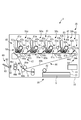
図1に示すように、画像形成装置1は、装置本体10と、シート給送部30と、画像形成部40と、シート排出部60と、制御部11とを備えている。尚、記録材であるシートSは、トナー像が形成されるものであり、具体例として、普通紙、普通紙の代用品である合成樹脂製のシート、厚紙、オーバーヘッドプロジェクタ用シート等がある。
As illustrated in FIG. 1, the image forming apparatus 1 includes an apparatus
シート給送部30は、装置本体10の下部に配置されており、シートSを積載して収容するシートカセット31と、給送ローラ32とを備え、シートSを画像形成部40に給送する。
The
画像形成部40は、画像形成ユニット50y,50m,50c,50kと、トナーボトル41y,41m,41c,41kと、露光装置42y,42m,42c,42kと、中間転写ユニット44と、二次転写部45と、定着部46とを備えている。尚、本実施の形態の画像形成装置1は、フルカラーに対応するものであり、画像形成ユニット50y,50m,50c,50kは、イエロー(y)、マゼンタ(m)、シアン(c)、ブラック(k)の4色それぞれに同様の構成で別個に設けられている。このため、図1中では4色の各構成について同符号の後に色の識別子を付して示すが、図2〜図5及び明細書中では色の識別子を付さずに符号のみで説明する場合もある。
The
画像形成ユニット50は、トナー画像を形成する感光ドラム(像担持体)51と、帯電ローラ(帯電手段)52と、現像装置(現像手段)53と、規制ブレード54とを備えている。感光ドラム51と帯電ローラ52は、不図示のドラムモータによって駆動される。
The
感光ドラム51は、アルミニウムシリンダの外周面に負極性の帯電極性を持つよう形成された感光層を有し、所定のプロセススピード(周速度)で矢印方向に回転する。帯電ローラ52には、不図示の高圧電源が接続されており、高電圧の帯電バイアス(帯電AC,帯電DC、図6参照)が印加される。帯電ローラ52は、感光ドラム51の表面に接触して、感光ドラム51の表面が均一に帯電される。即ち、帯電ローラ52は、帯電バイアスが印加されることにより、感光ドラム51を帯電する。感光ドラム51の表面では、帯電後、露光装置42によって画像情報に基づいて静電像が形成される。感光ドラム51は、形成された静電像を担持して、現像装置53に向けて周回移動する。
The
現像装置53では、不図示の高圧電源によって、現像スリーブ55に高電圧の現像バイアス(現像DC、図6参照)が印加される。負電荷のトナーが現像スリーブより正電位(現像スリーブ55より正、GNDに対して負)の潜像に現像され、一次転写ローラ(転写手段)47の方向に回転していく。即ち、現像装置53は、現像バイアスが印加されることにより、感光ドラム51上(像担持体上)に形成された静電像をトナーで現像する。感光ドラム51に現像されたトナー像は、後述する中間転写ベルト44bに一次転写される。規制ブレード54は、感光ドラム51の表面に接して配置され、感光ドラム51の表面に残留する転写残留トナー等の残留物を清掃する。
In the developing
中間転写ユニット44は、駆動ローラ44aや従動ローラ44d、一次転写ローラ47y,47m,47c,47k等の複数のローラと、これらのローラに巻き掛けられ、トナー像を担持する中間転写ベルト(被転写材)44bとを備えている。一次転写ローラ47y,47m,47c,47kは、感光ドラム51y,51m,51c,51kにそれぞれ対向して配置され、中間転写ベルト44bに当接する。
The
中間転写ベルト44bに一次転写ローラ47によって正極性の直流高圧である一次転写バイアス(転写バイアス)を印加することにより、感光ドラム51上のそれぞれの負極性を持つトナー像が順次中間転写ベルト44bに多重転写される。即ち、一次転写ローラ47は、一次転写バイアス(一次転写電圧、図6参照)が印加されることにより、感光ドラム51上に形成されたトナー像を転写位置において中間転写ベルト44bに転写する。二次転写部45は、二次転写内ローラ45aと、二次転写外ローラ45bとを備えている。二次転写外ローラ45bに正極性の直流高圧である二次転写バイアスを印加することによって、中間転写ベルト44bに形成されたフルカラーのトナー像をシートSに転写する。定着部46は、定着ローラ46a及び加圧ローラ46bを備えている。定着ローラ46aと加圧ローラ46bとの間をシートSが挟持され搬送されることにより、シートSに転写されたトナー像は加熱及び加圧されてシートSに定着される。
By applying a primary transfer bias (transfer bias), which is a positive DC high voltage, to the
シート排出部60は、排出経路の下流側に配置された排出ローラ対61と、装置本体10の側部に配設された排出口62及び排出トレイ63とを備えている。排出ローラ対61は、排出経路から搬送されるシートSをニップ部から給送し、排出口62から排出可能である。排出口62から排出されたシートSは、排出トレイ63に積載される。
The
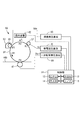
図2に示すように、制御部11はコンピュータにより構成され、例えばCPU12と、各部を制御するプログラムを記憶するROM13と、データを一時的に記憶するRAM14と、外部と信号を入出力する入出力回路(I/F)15とを備えている。CPU12は、画像形成装置1の制御全体を司るマイクロプロセッサであり、システムコントローラの主体である。CPU12は、入出力回路15を介して、シート給送部30、画像形成部40、シート排出部60に接続され、各部と信号をやり取りすると共に動作を制御する。
As shown in FIG. 2, the
制御部11は、帯電バイアスの立ち上がりを開始したときに帯電位置P1を通過した感光ドラム51の領域が転写位置P4を通過するタイミングに対応するように一次転写バイアスの立ち上がりを開始するように制御する(図6参照)。また、制御部11は、帯電バイアスの立ち上がりを完了したときに帯電位置P1を通過した感光ドラム51の領域が転写位置P4を通過するタイミングに対応するように一次転写バイアスの立ち上がりを完了するように制御する(図6参照)。ここで、本実施形態では、帯電バイアスの立ち上がりを開始したときに帯電位置P1を通過した感光ドラム51の領域が転写位置P4を通過するタイミングを、帯電開始領域通過時という。また、本実施形態では、帯電バイアスの立ち上がりを完了したときに帯電位置P1を通過した感光ドラム51の領域が転写位置P4を通過するタイミングを、帯電完了領域通過時という。
The
制御部11は、帯電開始領域通過時のタイミング以降、帯電完了領域通過時のタイミングまでに、一次転写バイアスの立ち上がりを開始するように制御する。また、制御部11は、帯電完了領域通過時以降、一次転写バイアスの立ち上がりを開始してから予め設定した所定時間で一次転写バイアスの立ち上がりを完了するように制御する。更に、制御部11は、一次転写バイアスの立ち上がりを開始してから完了するまでの全立上時間T3(図6参照)の間、感光ドラム51の表面電位と感光ドラム51に流れ込む一次転写電流との関係が所定範囲内になるように制御する。ここでの所定範囲とは、感光ドラム51の表面の帯電電位に一次転写バイアスの履歴が残ることによる横スジ等を発生させない領域である(図7(a)参照)。
The
制御部11は、帯電開始領域通過時と一次転写バイアスの立ち上がりを開始するタイミングとの差分時間が、帯電バイアスの立ち上がりを開始してから完了するまでの全立上時間T1(図6参照)の20%以内の時間になるように制御する。また、制御部11は、帯電開始領域通過時と一次転写バイアスの立ち上がりを開始するタイミングとの差分時間が、帯電バイアスの全立上時間T1(図6参照)の10%以内の時間になるように制御する。本実施形態では、制御部11は、帯電開始領域通過時と一次転写バイアスの立ち上がりを開始するタイミングとの差分時間を0とし、帯電開始領域通過時において一次転写バイアスの立ち上がりを開始するように制御する(図6参照)。
The
制御部11は、帯電完了領域通過時と一次転写バイアスの立ち上がりを完了するタイミングとの差分時間が、帯電バイアスの立ち上がりを開始してから完了するまでの全立上時間T1(図6参照)の20%以内の時間になるように制御する。また、制御部11は、帯電完了領域通過時と一次転写バイアスの立ち上がりを完了するタイミングとの差分時間が帯電バイアスの全立上時間T1(図6参照)の10%以内の時間になるように制御する。本実施形態では、制御部11は、帯電完了領域通過時と一次転写バイアスの立ち上がりを完了するタイミングとの差分時間を0とし、帯電完了領域通過時において一次転写バイアスの立ち上がりを完了するように制御する(図6参照)。
The
制御部11は、帯電バイアスの全立上時間T1と一次転写バイアスの全立上時間T3との重複時間が、帯電バイアス又は一次転写バイアスの全立上時間の70%以上の時間になるように制御する(図6参照)。また、制御部11は、上述した重複時間が、帯電バイアス又は一次転写バイアスの全立上時間の80%以上の時間になるように制御する。本実施形態では、上述した重複時間が、帯電バイアス又は一次転写バイアスの全立上時間の100%以上の時間、即ち一致するように制御する(図6参照)。
The
制御部11は、非画像形成時に一次転写ローラ47に所定の一次転写バイアスを印加し、その際に電流検出回路の検出結果より画像形成時の一次転写バイアスの電圧値を算出する。また、制御部11は、一次転写バイアスの立ち上げを開始してから完了するまでの全立上時間T3の間、一次転写バイアスを直線状に立ち上げる(図6参照)。尚、画像形成時とは、画像形成装置に備えられたスキャナやパーソナルコンピュータなどの外部端末から入力された画像情報に基づいて、感光ドラムにトナー像を形成しているときである。一方、非画像形成時とは、これ以外のときであり、例えば、画像形成ジョブ中の紙間や、画像形成ジョブが実行されていないときである。
The
制御部11は、帯電高圧基板70と、露光装置42と、現像高圧基板80と、一次転写高圧基板(転写バイアス出力手段)90とに接続されている。制御部11は、各高圧基板70,80,90を制御することで、帯電ローラ52、現像スリーブ55、一次転写ローラ47に高電圧を供給する。帯電高圧基板70は、帯電ローラ52に帯電バイアスVc(AC高電圧に負のDC高電圧を重畳した高電圧)を出力して、感光ドラム51の表面(感光面)を帯電させる。露光装置42は、光源であるレーザダイオードをドライバ回路によって発光させる。そして、露光装置42は、書込み用のビーム状レーザ光Lを感光ドラム51の軸線方向(主走査方向)に走査して、矢印R1方向(副走査方向)に回転する感光ドラム51の帯電した表面を露光して、静電潜像を形成する。
The
現像高圧基板80は、現像スリーブ55に現像バイアスVde(負電圧)を出力して、その外周面に担持する現像剤中のトナーを帯電させる。そのトナーが感光ドラム51の表面に接触して、静電潜像において露光されて負の帯電電位が減少した画素に付着して現像し、感光ドラム51の表面にトナー像を形成する。一次転写高圧基板90は、一次転写ローラ47に一次転写バイアスVtr1(トナー像の帯電極性と反対の正電圧)を出力し、感光ドラム51の表面のトナー像を一次転写ローラ47側に引き付けて、中間転写ベルト44b上に転写させる。
The developing high-
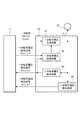
次に、画像形成装置1の感光ドラム51の周りのプロセス構成に高圧を供給する高圧基板の構成例について、図3〜図5を用いて説明する。
Next, a configuration example of a high-pressure substrate that supplies a high pressure to the process configuration around the
図3に示すように、制御部11は、帯電高圧基板70に対して、帯電AC高圧のVppを設定する帯電AC電圧設定信号Vcont_cacと、帯電AC高圧波形の周波数を決定する帯電ACクロックCLK1と、を出力する。また、制御部11は、帯電高圧基板70に対して、帯電DC高圧生成回路72の不図示のトランスの駆動を行う帯電DCクロックCLK2と、帯電高圧基板70のDC高圧の電圧値を設定する帯電DC電圧設定信号Vcont_cdcと、を出力する。
As shown in FIG. 3, the
帯電高圧基板70は、帯電AC高圧生成回路71と、帯電DC高圧生成回路72と、帯電DC電圧制御回路73と、帯電AC電圧検出回路74と、帯電DC電圧検出回路75とを有している。帯電高圧基板70は、制御部11の信号に基づいて高電圧を出力し、帯電ローラ52へ供給している。制御部11の信号に基づいて、帯電AC高圧生成回路71及び帯電DC高圧生成回路72が動作し、各回路で生成された出力を重畳して出力する。
The charging high-
帯電DC電圧制御回路73は、帯電DC電圧設定信号Vcont_cdcと帯電DC電圧検出回路75で検出した帯電DC電圧検出信号Vsns_cdcが一致するように、フィードバック制御を実行する。帯電DC電圧検出回路75は、帯電DC高圧生成回路72の出力電圧を検出し、帯電DC電圧検出信号Vsns_cdcを帯電DC電圧制御回路73に入力する。帯電DC高圧生成回路72は、帯電DCクロックCLK2によって不図示のトランスの一次側を駆動し、帯電DC電圧設定信号Vcont_cdcで設定された電圧の負電位のDC高圧を生成し出力する。
The charging DC
帯電AC高圧生成回路71は、帯電ACクロックCLK1の周波数で帯電AC電圧設定信号Vcont_cacにより設定された振幅の正弦波のAC高圧を出力する。帯電AC電圧検出回路74は、帯電AC高圧生成回路71から出力されたAC高圧のVppを検出し、Vppに応じた交流電圧の帯電AC電圧検出信号Vsns_cacを帯電AC高圧生成回路71に出力する。帯電AC高圧生成回路71は、帯電AC電圧設定信号Vcont_cacと入力された帯電AC電圧検出信号Vsns_cacとが一致するようにフィードバック制御がされており、交流と直流とを重畳した電圧を帯電ローラ52に出力する。
The charging AC high
図4に示すように、制御部11は、現像高圧基板80に対して、現像DC高圧生成回路81の不図示のトランスの駆動を行う現像DCクロックCLK3と、現像高圧基板80のDC高圧の電圧値を設定する現像DC電圧設定信号Vcont_deとを出力する。
As shown in FIG. 4, the
現像高圧基板80は、現像DC電圧制御回路82、現像DC高圧生成回路81、現像DC電圧検出回路83とを有し、制御部11の信号に基づいて負電位の高電圧を出力し、現像スリーブ55へ供給している。現像DC電圧制御回路82は、現像DC電圧設定信号Vcont_deと現像DC電圧検出回路83で検出した現像DC電圧検出信号Vsns_deとが一致するようにフィードバック制御がされており、負電位のDCの高電圧が現像スリーブ55に出力される。現像DC電圧検出回路83は、現像DC高圧生成回路81の出力電圧を検出し、現像DC電圧検出信号Vsns_deを現像DC電圧制御回路82に入力する。現像DC高圧生成回路81は、現像DCクロックCLK3によって不図示のトランスの一次側を駆動し、現像DC電圧設定信号Vcont_deで設定された電圧のDC高圧を生成し出力する。
The development
図5に示すように、制御部11は、一次転写高圧基板90に対して、一次転写高圧生成回路91の不図示のトランスの駆動を行う一次転写クロックCLK4を出力する。また、制御部11は、一次転写高圧基板90に対して、と、一次転写高圧基板90のDC高圧の電圧値を設定する一次転写電圧設定信号Vcont_tr1を出力する。
As shown in FIG. 5, the
一次転写高圧基板90は、一次転写電圧制御回路92、一次転写高圧生成回路91、一次転写電圧検出回路93、一次転写電流検出回路(電流検出回路)94とを有し、制御部11の信号に基づいて高電圧を出力し、一次転写ローラ47へ供給している。一次転写電圧制御回路92は、一次転写電圧設定信号Vcont_tr1と一次転写電圧検出回路93で検出した一次転写電圧検出信号Vsns_tr1とが一致するようにフィードバック制御しており、直流の高電圧を一次転写ローラ47に出力する。
The primary transfer
一次転写電圧検出回路93は、一次転写高圧生成回路91の出力電圧を検出し、一次転写電圧検出信号Vsns_tr1を一次転写電圧制御回路92及び制御部11に入力する。一次転写高圧生成回路91は、一次転写クロックCLK4によって不図示のトランスの一次側を駆動し、一次転写電圧設定信号Vcont_tr1で設定された電圧のDC高圧を生成し出力する。
The primary transfer
一次転写電流検出回路94は、画像形成装置1の非画像形成時に一次転写高圧基板90の出力電流を検出し、制御部11に一次転写電流検出信号Isns_tr1を出力する。即ち、一次転写電流検出回路94は、一次転写ローラ47に流れる電流を検出可能である。制御部11は、一次転写電流検出信号Isns_tr1から一次転写ローラ47の抵抗値を算出し、画像形成装置1の画像形成時に一次転写ローラ47に印加する一次転写出力電圧値を算出する制御(ATVC)を実行する。即ち、本実施形態の画像形成装置1では、制御部11は、感光ドラム51上の非画像部に対し一次転写部を予め設定された値で定電圧制御する。そして、制御部11は、このときの設定電圧値及び一次転写ローラ47に流れる電流値により一次転写ローラ47の抵抗値を算出し、画像形成時には画像形成装置1の使用環境や耐久状況を考慮して決定された電圧値で定電圧制御する(ATVC)。
The primary transfer
ここで、本実施形態の画像形成装置1における感光ドラムの周上の高圧印加の動作の説明に先立ち、比較例としての画像形成装置における動作を説明する。図10に、比較例としての画像形成装置における感光ドラムの周上の同一箇所に対する各高圧の印加状態を示す。尚、画像形成装置は、非画像形成時にATVC制御を実行し、画像形成時に一次転写ローラに印加する一次転写出力電圧値を算出するものとする。 Here, prior to the description of the operation of applying a high voltage on the periphery of the photosensitive drum in the image forming apparatus 1 of the present embodiment, the operation in the image forming apparatus as a comparative example will be described. FIG. 10 shows the applied state of each high voltage to the same location on the periphery of the photosensitive drum in the image forming apparatus as a comparative example. Note that the image forming apparatus executes ATVC control during non-image formation and calculates a primary transfer output voltage value applied to the primary transfer roller during image formation.
図10において、横軸は時間軸を示すが、各高圧の出力波形は感光ドラムの表面の周上の同一箇所に印加される出力値が時間軸の同じポイントに示されている。即ち、帯電ACが起動してから150ms後に帯電DCが起動し、帯電DCは150ms以内に−700Vまで立ち上がる。また、帯電DCが起動した際の帯電位置P1が現像位置P3に到達するタイミングで現像DCが起動し、現像DCは150ms以内に−450Vまで立ち上がる。更に、現像DCが起動した際の現像位置P3が転写位置P4に到達し、それから150ms後に一次転写電圧が起動する。 In FIG. 10, the horizontal axis indicates the time axis, but in each high voltage output waveform, the output value applied to the same location on the circumference of the surface of the photosensitive drum is shown at the same point on the time axis. That is, the charging DC is activated 150 ms after the activation of the charging AC, and the charging DC rises to −700 V within 150 ms. Further, the development DC is activated at the timing when the charging position P1 when the charging DC is activated reaches the development position P3, and the development DC rises to −450 V within 150 ms. Further, the development position P3 when the development DC is activated reaches the transfer position P4, and the primary transfer voltage is activated 150 ms later.
一次転写高圧の出力開始から一次転写高圧がATVCで得られた目標電圧値に安定するまでの見積もり時間である120ms経過後、画像形成動作開始のトリガ信号IMG_ENが制御部から出力される。IMG_ENは、露光装置に感光ドラムの表面をレーザ光Lで露光する書き込み動作を指示する信号である。 A trigger signal IMG_EN for starting the image forming operation is output from the control unit after 120 ms, which is an estimated time from the start of the primary transfer high voltage output until the primary transfer high voltage is stabilized at the target voltage value obtained by ATVC. IMG_EN is a signal that instructs the exposure apparatus to perform a writing operation for exposing the surface of the photosensitive drum with the laser beam L.
この画像形成装置では、一次転写高圧の出力開始から一次転写高圧がATVCで得られた目標電圧値に安定するまでの見積もり時間を120msとしたが、その理由は以下の通りである。一次転写高圧は、出力電流値が所望の値(例えば40μA)になるように出力電圧値が調整されて出力される。しかし、この立ち上がり電圧・電流波形は、画像形成装置の使用環境や耐久状況等によって発生する一次転写ローラのインピーダンスのばらつきにより異なったものとなる。電流波形b1は、一次転写ローラのインピーダンスが(画像形成装置の使用環境や耐久状況等を考慮して)最も小さい場合であり、一次転写高圧の出力開始後、出力電流値が40μAに安定するまでの時間は50msである。また、この時の出力電圧波形は、電圧波形a1のようになる。電流波形b2は、一次転写ローラのインピーダンスが(画像形成装置の使用環境や耐久状況等を考慮して)標準的な場合であり、一次転写高圧の出力開始後、出力電流値が40μAに安定するまでの時間は80msである。また、この時の出力電圧波形は、電圧波形a2のようになる。電流波形b3は、一次転写ローラのインピーダンスが(画像形成装置の使用環境や耐久状況等を考慮して)最も大きい場合であり、一次転写高圧の出力開始後、出力電流値が40μAに安定するまでの時間は120msである。また、この時の出力電圧波形は、電圧波形a3のようになる。このため、前述の一次転写ローラのインピーダンスのばらつき等を考慮して、最も一次転写出力の立ち上がりが遅い場合である電流波形b3を見込んで時間を見積もる必要があるため、見積もり時間を120msとしている。 In this image forming apparatus, the estimated time from the start of primary transfer high voltage output to the stabilization of the primary transfer high voltage to the target voltage value obtained by ATVC is 120 ms. The reason is as follows. The primary transfer high voltage is output with the output voltage value adjusted so that the output current value becomes a desired value (for example, 40 μA). However, the rising voltage / current waveform varies depending on the impedance variation of the primary transfer roller, which occurs depending on the usage environment and durability of the image forming apparatus. The current waveform b1 is the case where the impedance of the primary transfer roller is the smallest (in consideration of the use environment and durability of the image forming apparatus), and until the output current value stabilizes to 40 μA after the start of the primary transfer high voltage output. Is 50 ms. Further, the output voltage waveform at this time is as shown by a voltage waveform a1. The current waveform b2 is a case where the impedance of the primary transfer roller is standard (in consideration of the use environment and durability of the image forming apparatus), and the output current value is stabilized at 40 μA after the output of the primary transfer high voltage is started. The time until is 80 ms. Further, the output voltage waveform at this time is as shown by a voltage waveform a2. The current waveform b3 is the case where the impedance of the primary transfer roller is the highest (in consideration of the use environment and durability of the image forming apparatus), and until the output current value stabilizes to 40 μA after the output of the primary transfer high voltage is started. Is 120 ms. Further, the output voltage waveform at this time is as shown by a voltage waveform a3. For this reason, the estimated time is set to 120 ms because it is necessary to estimate the time by considering the current waveform b3, which is the case where the rise of the primary transfer output is the slowest, in consideration of the impedance variation of the primary transfer roller described above.
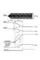
次に、本実施形態の画像形成装置1における感光ドラム51の周上の高圧印加の動作について、図6及び図7に沿って説明する。尚、画像形成装置1は、非画像形成時にATVC制御を実行し、画像形成時に一次転写ローラに印加する一次転写出力電圧値を算出するものとする。
Next, the operation of applying a high voltage on the periphery of the
図6において、横軸は時間軸を示すが、各高圧の出力波形は感光ドラム51の表面の周上の同一箇所に印加される出力値が時間軸の同じポイントに示されている。即ち、帯電ACが起動してから150ms後に帯電DCが起動し、帯電DCは150ms後に0Vから目標バイアスである−700Vまで傾斜した線形的なスロープ状(直線状)に立ち上がる。また、帯電DCが起動した際の帯電位置P1が現像位置P3に到達するタイミングで現像DCが起動し、現像DCは150ms後に0Vから目標バイアスである−450Vまで傾斜した線形的なスロープ状(直線状)に立ち上がる。更に、現像DCが起動した際の現像位置P3が転写位置P4に到達するタイミングで一次転写電圧が起動し、一次転写電圧は150ms後に目標バイアスである1300Vまで線形的なスロープ状(直線状)に立ち上がる。ここで、各バイアスにおいて、バイアスの立ち上り開始から目標バイアスに到達した立ち上り完了までの時間を、全立上時間とする。本実施形態では、帯電DCの全立上時間T1と、現像DCの全立上時間T2と、一次転写電圧の全立上時間T3とは、いずれも150msで同一長さとしている。
In FIG. 6, the horizontal axis indicates the time axis, but in each high voltage output waveform, the output value applied to the same location on the circumference of the surface of the
従来の画像形成装置では、制御部は、一次転写電圧設定信号Vcont_tr1の信号レベルを、一次転写電圧が0Vの設定レベルV_0から1300Vの設定レベルV_1300まで一気に直接切り換えている(図中、破線で示す)。この場合、一次転写電圧は高速に立ち上がり(図中、破線で示す)、感光ドラムの表面の帯電電位の段差が大きくなり横スジが発生してしまう可能性がある。 In the conventional image forming apparatus, the control unit directly switches the signal level of the primary transfer voltage setting signal Vcont_tr1 from the setting level V_0 where the primary transfer voltage is 0 V to the setting level V_1300 where the primary transfer voltage is 1300 V (indicated by a broken line in the drawing). ). In this case, the primary transfer voltage rises at a high speed (indicated by a broken line in the drawing), and there is a possibility that a step of the charged potential on the surface of the photosensitive drum becomes large and a horizontal stripe is generated.
これに対し、本実施形態の画像形成装置1は、制御部11は、一次転写電圧設定信号Vcont_tr1の信号レベルを、一次転写電圧が0Vの設定レベルV_0から1300Vの設定レベルV_1300まで切り換えている。この切り換えは、傾斜した線形的なスロープ状(直線状)としている。その結果、一次転写電圧は、スロープ時間150msの間に0Vから1300Vまで変化する。
In contrast, in the image forming apparatus 1 of the present embodiment, the
一次転写高圧のスロープ時間は、一次転写ローラ47のインピーダンスのばらつき等を考慮し、従来の画像形成装置のように設定レベルを一気に直接切り換えた場合の一次転写高圧出力の立ち上がりに必要な最長時間よりも長く設定する。このため、本実施形態では、一次転写電圧設定信号Vcont_tr1の信号レベルを設定レベルV_0から設定レベルV_1300まで直接切り替えた場合に一次転写高圧出力の立ち上がりに必要な最長時間120msよりも長い150msとしている。これにより、制御部11は、一次転写高圧の出力開始から150ms経過後、画像形成動作開始のトリガ信号IMG_ENを出力する。IMG_ENは、露光装置42に感光ドラム51の表面をレーザ光Lで露光する書き込み動作を指示する信号である。
The slope time of the primary transfer high pressure is longer than the maximum time required for the rise of the primary transfer high pressure output when the setting level is switched directly at once like the conventional image forming apparatus in consideration of the impedance variation of the
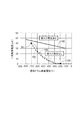
次に、制御部11が感光ドラム51の表面電位と感光ドラム51に流れ込む転写電流との関係を、出力画像に横スジ等を発生させない所定範囲について説明する。図7(a)において、実線100よりも下側の領域は、前述した感光ドラム51の表面の帯電電位に一次転写バイアスの履歴が残ることによる横スジ等を発生させない領域(所定範囲)であり、実線100よりも上側の領域は、横スジ等を発生させる領域である。ここで、本実施形態では、横スジの定義としては、同一シートに濃度が一様な画像を形成しようとした場合に適正濃度に対する濃度差が0.2よりも大きくなる濃度ムラとしている。また、図7(a)に示す例では、濃度は、反射濃度計(X−Rite社製、反射濃度計モデル504)により測定している。尚、本実施形態の感光ドラム51は暗減衰無しの特性を有しており、感光ドラム51に印加される帯電バイアスの電圧値が感光ドラム51の表面の周上の同一箇所が転写位置P4に来た時の感光ドラム51の表面電位と同じになる。
Next, the relationship between the surface potential of the
本実施形態において、一次転写出力電圧は、感光ドラム51の表面電位が−700Vの時に一次転写電流が40μAとなる電圧(1300V)が設定されている(図7(a)中、点101)。点101は実線100よりも下側の領域であり、前述した感光ドラム51の表面の帯電電位に一次転写バイアスの履歴が残ることによる横スジ等が発生しない領域に位置する。一次転写電流は感光ドラム51の表面電位と一次転写ローラ47との電位差により発生する放電電流であり、感光ドラム51の表面電位と一次転写ローラ47の電位差ΔVと一次転写電流との関係は、パッシェンの法則により定義される。
In this embodiment, the primary transfer output voltage is set to a voltage (1300 V) at which the primary transfer current is 40 μA when the surface potential of the
図7(a)に示す破線102は、図7(b)に示すΔVと一次転写電流の関係を基にした感光ドラム51の表面電位と一次転写電流との関係を示す。例えば、図7(a)の点103は図7(b)の点104に相当し、ΔVが500Vになった時に一次転写ローラ47から感光ドラム51の表面への放電が開始され、一次転写電流が流れ始めるポイントである。この時の感光ドラム51の表面電位は−200V、一次転写出力電圧は300Vとなる。図7(a)の点101は図7(b)の点105に相当し、ΔVが2000V、一次転写電流が40μAとなるポイントである。この時の感光ドラム51の表面電位は−700V、一次転写出力電圧は1300Vとなる。
A
また、制御部11は、前述したATVCを実施することにより、一次転写ローラ47の抵抗値が分かるため、感光ドラム51の表面電位との関係から一次転写出力電圧と一次転写出力電流の関係を算出できる。本実施形態では、制御部11は、一次転写出力電流値が図7(a)の破線102に示すような値となるように、一次転写出力電圧を制御している。このように一次転写出力をスロープ状に立ち上げた場合、一次転写電圧が0Vから1300Vまで変化する際、一次転写電流値は図7(a)の破線102に示すように変化する。このため、一次転写電流値は、常に図7(a)の実線100よりも下側の領域となるため、前述した感光ドラム51の表面の帯電電位に一次転写バイアスの履歴が残ることによる横スジ等は発生しない。
Further, since the
上述したように本実施形態の画像形成装置1によれば、制御部11は、帯電開始領域通過時に対応するように、転写バイアスの立ち上がりを開始するように制御する。また、制御部11は、帯電完了領域通過時に、転写バイアスの立ち上がりを完了するように制御する。このため、帯電バイアスの立ち上がりを完了したときに帯電位置P1を通過した感光ドラム51の領域が転写位置P4を通過するタイミング後に転写バイアスの立ち上がりを開始する場合に比べて、FCOTを短縮することができる。
As described above, according to the image forming apparatus 1 of the present embodiment, the
また、本実施形態の画像形成装置1によれば、制御部11は、帯電開始領域通過時以降、帯電完了領域通過時までに、一次転写バイアスの立ち上がりを開始する。また、制御部11は、帯電完了領域通過時以降、一次転写バイアスの立ち上がりを開始してから予め設定した所定時間で一次転写バイアスの立ち上がりを完了する。このため、FCOTを大幅に短縮することができる。
Further, according to the image forming apparatus 1 of the present embodiment, the
また、本実施形態の画像形成装置1によれば、制御部11は、一次転写バイアスの立ち上げを開始してから完了するまでの全立上時間T3の間、感光ドラム51の表面電位と感光ドラム51に流れ込む転写電流との関係が所定範囲内になるように制御する。このため、感光ドラム51の表面の負電位の帯電が不十分な状態で一次転写バイアスを印加してポジ帯電させてしまうことを防止して、帯電電位のムラを低減し、出力画像の濃度段差や横スジの発生を抑制することができる。
Further, according to the image forming apparatus 1 of the present embodiment, the
また、本実施形態の画像形成装置1によれば、一次転写高圧を帯電位置P1及び現像位置P3で各々帯電DC高圧と現像DC高圧の立ち上げを開始した感光ドラム51の表面の周上の同一箇所が転写位置P4に来たタイミングでスロープ状に立ち上げている。一次転写高圧出力の立ち上げをスロープ状にしているため、帯電出力と一次転写出力の電位差を横スジが発生しない所定の範囲に保持しながら高圧出力を立ち上げることが可能となる。よって、従来の画像形成装置1において費やしていた120ms分(図10参照)のFCOTを短縮することが可能となる。
Further, according to the image forming apparatus 1 of the present embodiment, the primary transfer high voltage is the same on the circumference of the surface of the
また、本実施形態の画像形成装置1によれば、帯電バイアス及び一次転写バイアスの各全立上時間T1,T3は完全に重なっている。このため、帯電バイアスの全立上時間T1に対する一次転写バイアスの全立上時間T3が重なる割合は、100%である。このため、特に効率よく帯電電位のムラを低減し、出力画像の濃度段差や横スジの発生を効果的に抑制することができる。 Further, according to the image forming apparatus 1 of the present embodiment, the total rising times T1 and T3 of the charging bias and the primary transfer bias are completely overlapped. For this reason, the ratio of the total rise time T3 of the primary transfer bias to the total rise time T1 of the charging bias is 100%. For this reason, the unevenness of the charging potential can be reduced particularly efficiently, and the generation of density steps and horizontal stripes in the output image can be effectively suppressed.
尚、上述した第1の実施形態の画像形成装置1では、タンデム型の画像形成装置1に適用した場合について説明したが、これには限られない。例えば、他の方式の画像形成装置であってもよく、また、フルカラーであることにも限られず、モノクロやモノカラーであってもよい。あるいは、プリンタ、各種印刷機、複写機、FAX、複合機等、種々の用途で実施することができる。また、本実施の形態では、画像形成装置1は、中間転写ベルト44bを有し、感光ドラム51から中間転写ベルト44bに各色のトナー像を一次転写した後、各色の複合トナー像をシートSに一括して二次転写する方式としている。但し、これには限られず、シート搬送ベルトで搬送されたシートに感光ドラムから直接に転写する方式を採用してもよい。この場合、例えば、感光ドラムの表面に形成したトナー像をシート(被転写材)に転写する転写手段への転写バイアス出力を、上述した実施形態における一次転写バイアス出力と同様に制御すればよい。
In addition, although the case where the image forming apparatus 1 according to the first embodiment is applied to the tandem type image forming apparatus 1 has been described, the present invention is not limited thereto. For example, other types of image forming apparatuses may be used, and the image forming apparatus is not limited to full color, and may be monochrome or monocolor. Alternatively, the present invention can be implemented for various uses such as a printer, various printing machines, a copying machine, a FAX, and a multifunction machine. In the present embodiment, the image forming apparatus 1 includes the
また、上述した第1の実施形態の画像形成装置1では、一次転写高圧出力のスロープ状の全立上時間T3を帯電高圧出力及び現像高圧出力のスロープ状の全立上時間T1,T2と同じ150msに設定しているが、これには限られない。即ち、図7(a)の実線100よりも下側の横スジ発生を起こさない領域に入るように、帯電DC高圧出力電圧と一次転写高圧出力電圧との電位差を保持できれば良い。このため、一次転写高圧出力のスロープ状の全立上時間T3を、帯電高圧出力及び現像高圧出力のスロープ状の全立上時間T1,T2より長くしてもよく、あるいは短くしてもよい。
In the image forming apparatus 1 of the first embodiment described above, the slope-like total rise time T3 of the primary transfer high-voltage output is the same as the slope-like total rise times T1, T2 of the charging high-voltage output and the development high-voltage output. Although it is set to 150 ms, it is not limited to this. That is, it is only necessary to maintain the potential difference between the charging DC high voltage output voltage and the primary transfer high voltage output voltage so as to enter a region where no horizontal streaking occurs below the
例えば、図6に示す実施形態では、制御部11は、帯電バイアスの立ち上がりを開始したときに帯電位置P1を通過した感光ドラム51の領域が転写位置P4を通過するタイミングで、一次転写バイアスの立ち上がりを開始するように制御する。即ち、感光ドラム51の帯電バイアスの印加開始位置が転写位置P4に到達すると同時に、一次転写バイアスが印加開始される。この場合、感光ドラム51の帯電バイアスの印加開始位置が転写位置P4に到達した到達時から、一次転写バイアスが印加開始される開始時までの開始時間差分が、ゼロになる。また、図6に示す実施形態では、制御部11は、帯電バイアスの立ち上がりを完了したときに帯電位置P1を通過した感光ドラム51の領域が転写位置P4を通過するタイミングで、一次転写バイアスの立ち上がりを完了するように制御する。即ち、感光ドラム51の帯電バイアスの印加完了位置が転写位置P4に到達すると同時に、一次転写バイアスが印加完了される。この場合、感光ドラム51の帯電バイアスの印加完了位置が転写位置P4に到達した到達時から、一次転写バイアスが印加完了される完了時までの完了時間差分が、ゼロになる。
For example, in the embodiment shown in FIG. 6, the
しかしながら、上述したように、開始時間差分及び完了時間差分は、いずれもゼロでなくても良い。制御部11は、帯電バイアスの立ち上がりを開始したときに帯電位置P1を通過した感光ドラム51の領域が転写位置P4を通過するタイミングに対応するように、一次転写バイアスの立ち上がりを開始するように制御できる。また、制御部11は、帯電バイアスの立ち上がりを完了したときに帯電位置P1を通過した感光ドラム51の領域が転写位置P4を通過するタイミングに対応するように、一次転写バイアスの立ち上がりを完了するように制御できる。
However, as described above, neither the start time difference nor the completion time difference may be zero. The
上記タイミングに対応するように立上動作を制御するため、制御部11は、例えば、帯電開始領域通過時と一次転写バイアスの立ち上がりを開始するタイミングとの差分時間が、帯電バイアスの全立上時間T1の20%以内の時間になるように制御できる。即ち、感光ドラム51の帯電バイアスの印加開始位置が転写位置P4に到達するタイミングと一次転写バイアスが印加開始されるタイミングとが、上記の範囲で異なっていてもよい。あるいは、制御部11は、例えば、帯電完了領域通過時と一次転写バイアスの立ち上がりを完了するタイミングとの差分時間が、帯電バイアスの全立上時間T1の20%以内の時間になるように制御できる。即ち、感光ドラム51の帯電バイアスの印加完了位置が転写位置P4に到達するタイミングと一次転写バイアスが印加完了されるタイミングとが、上記の範囲で異なっていてもよい。これらの場合も、開始時間差分あるいは完了時間差分がゼロに近いので、帯電電位のムラを低減し、出力画像の濃度段差や横スジの発生を抑制することができる。
In order to control the start-up operation so as to correspond to the above timing, the
また、各差分時間が帯電バイアスの全立上時間T1の20%以内の時間になるように制御することには限られず、例えば、10%以内の時間になるように制御してもよい。この場合、より効果的に帯電電位のムラを低減することができ、より好ましい。 Further, the control is not limited to the time when each difference time is within 20% of the total rising time T1 of the charging bias. For example, the time may be controlled within 10%. In this case, the unevenness of the charging potential can be more effectively reduced, which is more preferable.
また、上述した本実施形態では、帯電バイアスの全立上時間T1に対する一次転写バイアスの全立上時間T3が重なる割合は100%であるが、これには限られない。制御部11は、帯電バイアスの全立上時間T1と、一次転写バイアスの全立上時間T3と、の重複時間が、帯電バイアス又は転写バイアスの全立上時間の70%以上の時間になるように制御してもよい。この場合も、帯電電位のムラを低減することができる。尚、上述の重複時間としては、帯電電位のムラを低減する観点より、帯電バイアス又は転写バイアスの全立上時間の80%以上の時間にすることがより好ましい。
In the present embodiment described above, the ratio of the total rise time T3 of the primary transfer bias to the total rise time T1 of the charging bias is 100%, but is not limited thereto. The
また、一次転写高圧出力のスロープ立ち上げ開始及び完了のタイミングは、感光ドラム51の表面の周上の同一箇所における帯電DC高圧出力及び現像DC高圧出力のスロープ立ち上げ開始及び完了のタイミングと一致させずに設定することも可能である。また、スロープの時間設定は、画像形成装置1の使用環境、帯電ローラ52や一次転写ローラ47の耐久状態、使用シート等の条件毎に設定することも可能である。
Further, the start timing and completion timing of the slope of the primary transfer high voltage output are made to coincide with the start timing and completion timing of the slope of the charging DC high voltage output and development DC high voltage output at the same location on the circumference of the surface of the
<第2の実施形態>
次に、本発明の第2の実施形態を、図8及び図9を参照しながら詳細に説明する。本実施形態では、一次転写電圧設定信号Vcont_tr1を所定時間毎に複数段階で切り替えて一次転写出力を立ち上げる点で、第1の実施形態と構成を異にしている。但し、それ以外の帯電高圧基板70、現像高圧基板80、一次転写高圧基板90等の構成や、高圧出力の制御動作は第1の実施形態と同様であるので、符号を同じくして詳細な説明を省略する。
<Second Embodiment>
Next, a second embodiment of the present invention will be described in detail with reference to FIGS. The present embodiment is different from the first embodiment in that the primary transfer voltage setting signal Vcont_tr1 is switched at a plurality of stages every predetermined time to raise the primary transfer output. However, the configuration of the other charged
図8において、横軸は時間軸を示すが、各高圧の出力波形は感光ドラム51の表面の周上の同一箇所に印加される出力値が時間軸の同じポイントに示されている。即ち、帯電ACが起動してから150ms後に帯電DCが起動し、帯電DCは150ms後に0Vから目標バイアスである−700Vまで傾斜した線形的なスロープ状(直線状)に立ち上がる。また、帯電DCが起動した際の帯電位置P1が現像位置P3に到達するタイミングで現像DCが起動し、現像DCは150ms後に0Vから目標バイアスである−450Vまで傾斜した線形的なスロープ状(直線状)に立ち上がる。
In FIG. 8, the horizontal axis indicates the time axis, but in each high voltage output waveform, the output value applied to the same location on the circumference of the surface of the
更に、現像DCが起動した際の現像位置P3が転写位置P4に到達するタイミングで一次転写電圧が起動し、一次転写電圧は150ms後に目標バイアスである1300Vまで5段階に段階的に立ち上がる。即ち、制御部11は、一次転写バイアスの立ち上げを開始してから完了するまでの全立上時間T3の間、一次転写バイアスを段階的に立ち上げる。
Furthermore, the primary transfer voltage is activated at the timing when the development position P3 when the development DC is activated reaches the transfer position P4, and the primary transfer voltage rises in five steps in stages up to the target bias of 1300 V after 150 ms. That is, the
まず、制御部11は、一次転写電圧設定信号Vcont_tr1を一次転写電圧出力電圧が0Vの設定レベルV_0から260Vの設定レベルV_260に切り換え、一次転写出力電圧を0Vから260Vまで変化させる。そして、制御部11は、一次転写電圧設定信号Vcont_tr1をV_0からV_260に切り換えてから30ms経過後、一次転写電圧設定信号Vcont_tr1を切り換える。ここでは、制御部11は、一次転写電圧設定信号Vcont_tr1を一次転写電圧出力電圧が260Vの設定レベルV_260から520Vの設定レベルV_520に切り換え、一次転写出力電圧を260Vから520Vまで変化させる。
First, the
また、制御部11は、一次転写電圧設定信号Vcont_tr1をV_260からV_520に切り換えてから30ms経過後、一次転写電圧設定信号Vcont_tr1を切り換える。ここでは、制御部11は、一次転写電圧設定信号Vcont_tr1を一次転写電圧出力電圧が520Vの設定レベルV_520から780Vの設定レベルV_780に切り換え、一次転写出力電圧を520Vから780Vまで変化させる。更に、制御部11は、一次転写電圧設定信号Vcont_tr1をV_520からV_780に切り換えてから30ms経過後、一次転写電圧設定信号Vcont_tr1を切り換える。ここでは、制御部11は、一次転写電圧設定信号Vcont_tr1を一次転写電圧出力電圧が780Vの設定レベルV_780から1040Vの設定レベルV_1040に切り換え、一次転写出力電圧を780Vから1040Vまで変化させる。そして、制御部11は、一次転写電圧設定信号Vcont_tr1をV_780からV_1040に切り換えてから30ms経過後、一次転写電圧設定信号Vcont_tr1を切り換える。ここでは、制御部11は、一次転写電圧設定信号Vcont_tr1を一次転写電圧出力電圧が1040Vの設定レベルV_1040から1300Vの設定レベルV_1300に切り換え、一次転写出力電圧を1040Vから1300Vまで変化させる。
In addition, the
この画像形成装置1では、一次転写高圧の出力開始から一次転写高圧がATVCで得られた目標電圧値に安定するまでの5段階の各立上時間を30msとしている。これは、各段階において一気に直接切り替えた場合に一次転写高圧出力の立ち上がりに必要な最長時間よりも長い時間としている。 In this image forming apparatus 1, each of the five stages of startup time from the start of primary transfer high voltage output to the stabilization of the primary transfer high voltage to the target voltage value obtained by ATVC is 30 ms. This is a time longer than the longest time required for the rising of the primary transfer high-voltage output when switching directly at each stage.
一次転写電圧設定信号Vcont_tr1を1040Vの設定レベルV_1040から1300Vの設定レベルV_1300に切り替えてから30ms経過後、制御部11は画像形成動作開始のトリガ信号IMG_ENを出力する。尚、本実施形態においても、帯電DCの全立上時間T1と、現像DCの全立上時間T2と、一次転写電圧の全立上時間T3とは、いずれも150msで同一長さとしている。
After switching the primary transfer voltage setting signal Vcont_tr1 from the setting level V_1040 of 1040V to the setting level V_1300 of 1300V, the
次に、制御部11が感光ドラム51の表面電位と感光ドラム51に流れ込む転写電流との関係を、出力画像に横スジ等を発生させない所定範囲について説明する。図9において、実線100よりも下側の領域は、前述した感光ドラム51の表面の帯電電位に一次転写バイアスの履歴が残ることによる横スジ等を発生させない領域(所定範囲)であり、実線100よりも上側の領域は、横スジ等を発生させる領域である。ここで、本実施形態においても、横スジの定義としては、同一シートに濃度が一様な画像を形成しようとした場合に適正濃度に対する濃度差が0.2よりも大きくなる濃度ムラとしている。また、図9に示す例では、濃度は、反射濃度計(X−Rite社製、反射濃度計モデル504)により測定している。尚、本実施形態の感光ドラム51は暗減衰無しの特性を有しており、感光ドラム51に印加される帯電バイアスの電圧値が感光ドラム51の表面の周上の同一箇所が転写位置P4に来た時の感光ドラム51の表面電位と同じになる。
Next, the relationship between the surface potential of the
図9に示す破線102は、図7(b)に示すΔVと一次転写電流の関係を基にした感光ドラム51の表面電位と一次転写電流との関係を示す。例えば、図9の点103は図7(b)の点104に相当し、ΔVが500Vになった時に一次転写ローラ47から感光ドラム51の表面への放電が開始され、一次転写電流が流れ始めるポイントである。この時の感光ドラム51の表面電位は−200V、一次転写出力電圧は300Vとなる。図9の点101は図7(b)の点105に相当し、ΔVが2000V、一次転写電流が40μAとなるポイントである。この時の感光ドラム51の表面電位は−700V、一次転写出力電圧は1300Vとなる。
A
図9の点線106は、図7(b)に示すΔVと一次転写電流との関係を基にした感光ドラム51の表面電位と一次転写電流との関係を示すものである。本実施形態のように一次転写出力を5段階で立ち上げた場合、図9の点線106に示すように一次転写電流が波状に変化し、破線102に比べて同じ感光ドラム51の表面電位に対して一次転写電流が大きくなるポイントがある。しかしながら、実線100よりは常に下側の領域にあるため、前述した感光ドラム51の表面の帯電電位に一次転写バイアスの履歴が残ることによる横スジは発生しない。
A dotted
上述したように本実施形態の画像形成装置1によっても、制御部11は、帯電開始領域通過時に対応するように、転写バイアスの立ち上がりを開始するように制御する。また、制御部11は、帯電完了領域通過時に、転写バイアスの立ち上がりを完了するように制御する。このため、帯電バイアスの立ち上がりを完了したときに帯電位置P1を通過した感光ドラム51の領域が転写位置P4を通過するタイミング後に転写バイアスの立ち上がりを開始する場合に比べて、FCOTを短縮することができる。
As described above, also in the image forming apparatus 1 of the present embodiment, the
また、制御部11は、一次転写バイアスの立ち上げを開始してから予め設定した所定時間で立ち上げを完了するように制御する。また制御部11は、帯電バイアスの立ち上がり完了時に帯電された感光ドラム51上の箇所が転写位置P4に位置した以降、一次転写バイアスの立ち上がりを完了する。更に、制御部11は、一次転写バイアスの立ち上げを開始してから完了するまでの間、感光ドラム51の表面電位と感光ドラム51に流れ込む転写電流との関係が所定範囲内になるように制御する。このため、感光ドラム51の表面の負電位の帯電が不十分な状態で一次転写バイアスを印加してポジ帯電させてしまうことを防止して、帯電電位のムラを低減し、出力画像の濃度段差や横スジの発生を抑制することができる。
In addition, the
また、本実施形態の画像形成装置1によれば、一次転写高圧の出力を5段階に切り換えているので、それぞれの段階で設定レベルを一気に直接切り換えても、出力画像の濃度段差や横スジの発生を抑制することができる。このため、一次転写高圧の出力をスロープ状に制御する場合に比べて、制御を容易に行うことができる。 In addition, according to the image forming apparatus 1 of the present embodiment, the output of the primary transfer high voltage is switched to five levels. Therefore, even if the set level is directly switched at each stage, the density step of the output image and the horizontal streak are changed. Occurrence can be suppressed. For this reason, control can be easily performed compared with the case where the output of the primary transfer high voltage is controlled in a slope shape.
尚、上述した第2の実施形態の画像形成装置1では、一次転写高圧の出力を5段階で各段階を立上時間30msで切り換えているが、これには限られず、切り換えの段階数や立上時間を適宜設定することができる。例えば、第2の実施形態のように段階ごとに立上時間を同じにしたり、あるいは段階ごとに立上時間を異ならせてもよい。即ち、図9に示す実線100よりも下側の横スジ発生を起こさない領域に入るように、帯電DC高圧出力電圧と一次転写高圧出力電圧との電位差を保持できれば良い。このため、一次転写高圧出力の段階状の全立上時間T3を、帯電高圧出力及び現像高圧出力のスロープ状の全立上時間T1,T2より長くしてもよく、あるいは短くしてもよい。
In the image forming apparatus 1 according to the second embodiment described above, the primary transfer high-voltage output is switched in five stages and each stage is switched at a start-up time of 30 ms. However, the present invention is not limited to this. The upper time can be set as appropriate. For example, the startup time may be the same for each stage as in the second embodiment, or the startup time may be different for each stage. That is, it is only necessary to maintain the potential difference between the charging DC high voltage output voltage and the primary transfer high voltage output voltage so as to enter the region where no horizontal streaking occurs below the
また、上述した本実施形態では、一次転写高圧値は30msごと5段階に切り換える場合について説明したが、これには限られない。一次転写高圧出力値の切換段数や切換時間は、画像形成装置1の使用環境、帯電ローラ52や一次転写ローラ47の耐久状態、使用シート等の条件毎に設定してもよい。
Further, in the above-described embodiment, the case where the primary transfer high-pressure value is switched to five stages every 30 ms is described, but the present invention is not limited to this. The number of switching stages and the switching time of the primary transfer high voltage output value may be set for each condition such as the usage environment of the image forming apparatus 1, the durability state of the charging
1…画像形成装置、11…制御部、44b…中間転写ベルト(被転写材)、47,47c,47k,47m,47y…一次転写ローラ(転写手段)、51,51c,51k,51m,51y…感光ドラム(像担持体)、52,52c,52k,52m,52y…帯電ローラ(帯電手段)、53,53c,53k,53m,53y…現像装置(現像手段)、90…一次転写高圧基板(転写バイアス出力手段)、94…一次転写電流検出回路(電流検出回路)、S…シート(被転写材)、T1…帯電バイアスの全立上時間、T2…現像バイアスの全立上時間、T3…一次転写バイアスの全立上時間(転写バイアスの全立上時間)。 DESCRIPTION OF SYMBOLS 1 ... Image forming apparatus, 11 ... Control part, 44b ... Intermediate transfer belt (transfer material), 47, 47c, 47k, 47m, 47y ... Primary transfer roller (transfer means), 51, 51c, 51k, 51m, 51y ... Photosensitive drum (image carrier), 52, 52c, 52k, 52m, 52y ... charging roller (charging means), 53, 53c, 53k, 53m, 53y ... developing device (developing means), 90 ... primary transfer high-pressure substrate (transfer) (Bias output means), 94 ... primary transfer current detection circuit (current detection circuit), S ... sheet (transfer material), T1 ... total rise time of charging bias, T2 ... total rise time of development bias, T3 ... primary Total rise time of transfer bias (total rise time of transfer bias).
Claims (14)
帯電バイアスが印加されることにより、前記像担持体と対向する帯電位置にて前記像担持体を帯電する帯電手段と、
現像バイアスが印加されることにより、前記像担持体上に形成された静電像をトナーで現像する現像手段と、
転写バイアスが印加されることにより、前記像担持体上に形成されたトナー像を転写位置において被転写材に転写する転写手段と、
前記転写バイアスを出力する転写バイアス出力手段と、
前記帯電バイアスの立ち上がりを開始したときに前記帯電位置を通過した前記像担持体の領域が前記転写位置を通過するタイミングに対応するように前記転写バイアスの立ち上がりを開始すると共に、前記帯電バイアスの立ち上がりを完了したときに前記帯電位置を通過した前記像担持体の領域が前記転写位置を通過するタイミングに対応するように前記転写バイアスの立ち上がりを完了するように制御する制御部と、を備える、
ことを特徴とする画像形成装置。 An image carrier;
A charging means for charging the image carrier at a charging position facing the image carrier by applying a charging bias;
Developing means for developing an electrostatic image formed on the image carrier with toner by applying a developing bias; and
A transfer means for transferring a toner image formed on the image carrier to a transfer material at a transfer position by applying a transfer bias;
Transfer bias output means for outputting the transfer bias;
The rise of the transfer bias is started so as to correspond to the timing at which the area of the image carrier that has passed the charge position passes the transfer position when the rise of the charge bias is started. A control unit that controls to complete the rising of the transfer bias so that the region of the image carrier that has passed the charging position when the charging is completed corresponds to the timing of passing the transfer position.
An image forming apparatus.
ことを特徴とする請求項1に記載の画像形成装置。 The control unit is configured to start the charging position when the rising of the charging bias is completed after the timing when the area of the image carrier that has passed the charging position passes the transfer position when the charging bias starts to rise. The image carrier that has started rising of the transfer bias by the time when the region of the image carrier that has passed through the transfer position passes through the transfer position, and has passed the charge position when the rise of the charge bias is completed. After the timing when the region passes through the transfer position, the transfer bias rise is completed in a predetermined time after starting the transfer bias rise.
The image forming apparatus according to claim 1.
ことを特徴とする請求項1又は2に記載の画像形成装置。 The controller controls the relationship between the surface potential of the image carrier and the transfer current flowing into the image carrier within a predetermined range during the entire rise time from the start to the completion of the transfer bias. To be controlled,
The image forming apparatus according to claim 1, wherein:
ことを特徴とする請求項1乃至3のいずれか1項に記載の画像形成装置。 The control unit determines a difference time between a timing at which the area of the image carrier that has passed the charging position when the charging bias starts to rise and a timing at which the transfer bias starts to rise. , And control to be within 20% of the total rise time from the start to the completion of the rise of the charging bias,
The image forming apparatus according to claim 1, wherein the image forming apparatus is an image forming apparatus.
ことを特徴とする請求項4に記載の画像形成装置。 The control unit controls the difference time to be a time within 10% of the total rise time of the charging bias.
The image forming apparatus according to claim 4.
ことを特徴とする請求項5に記載の画像形成装置。 The controller sets the difference bias to 0, and at the timing when the area of the image carrier that has passed the charging position passes the transfer position when the charging bias starts rising, the transfer bias rises. Control to start,
The image forming apparatus according to claim 5.
ことを特徴とする請求項1乃至6のいずれか1項に記載の画像形成装置。 The controller is configured such that when the rising of the charging bias is completed, a difference time between a timing at which the area of the image carrier that has passed the charging position passes the transfer position and a timing at which the rising of the transfer bias is completed. , And control to be within 20% of the total rise time from the start to the completion of the rise of the charging bias,
The image forming apparatus according to claim 1, wherein the image forming apparatus is an image forming apparatus.
ことを特徴とする請求項7に記載の画像形成装置。 The control unit controls the difference time to be a time within 10% of the total rise time of the charging bias.
The image forming apparatus according to claim 7.
ことを特徴とする請求項8に記載の画像形成装置。 The control unit sets the difference bias to 0, and raises the transfer bias at a timing when the area of the image carrier that has passed the charging position passes the transfer position when the charging bias rise is completed. Control to complete,
The image forming apparatus according to claim 8.
ことを特徴とする請求項1乃至9のいずれか1項に記載の画像形成装置。 The control unit has an overlap time between the total rise time from the start of the rising of the charging bias to the completion and the total rise time from the start of the transfer bias to the completion, Control to be 70% or more of the total rise time from the start of the rise of the charging bias or the transfer bias to the completion thereof,
The image forming apparatus according to claim 1, wherein the image forming apparatus is an image forming apparatus.
ことを特徴とする請求項10に記載の画像形成装置。 The control unit controls the overlap time to be 80% or more of the total rise time of the charging bias or the transfer bias.
The image forming apparatus according to claim 10.
前記制御部は、非画像形成時に前記転写手段に所定の転写バイアスを印加し、その際に前記電流検出回路の検出結果より画像形成時の前記転写バイアスの電圧値を算出する、
ことを特徴とする請求項1乃至11のいずれか1項に記載の画像形成装置。 A current detection circuit capable of detecting a current flowing through the transfer means;
The control unit applies a predetermined transfer bias to the transfer unit at the time of non-image formation, and calculates a voltage value of the transfer bias at the time of image formation from a detection result of the current detection circuit at that time.
The image forming apparatus according to claim 1, wherein the image forming apparatus is an image forming apparatus.
ことを特徴とする請求項1乃至12のいずれか1項に記載の画像形成装置。 The controller raises the transfer bias linearly during the entire rise time from the start of raising the transfer bias to completion.
The image forming apparatus according to claim 1, wherein the image forming apparatus is an image forming apparatus.
ことを特徴とする請求項1乃至12のいずれか1項に記載の画像形成装置。
The controller raises the transfer bias in a stepwise manner during the entire rise time from the start of the transfer bias to completion.
The image forming apparatus according to claim 1, wherein the image forming apparatus is an image forming apparatus.
Priority Applications (2)
| Application Number | Priority Date | Filing Date | Title |
|---|---|---|---|
| JP2016120233A JP2017223874A (en) | 2016-06-16 | 2016-06-16 | Image forming apparatus |
| US15/623,840 US10656580B2 (en) | 2016-06-16 | 2017-06-15 | Image forming apparatus controlling charging bias and transfer bias |
Applications Claiming Priority (1)
| Application Number | Priority Date | Filing Date | Title |
|---|---|---|---|
| JP2016120233A JP2017223874A (en) | 2016-06-16 | 2016-06-16 | Image forming apparatus |
Publications (2)
| Publication Number | Publication Date |
|---|---|
| JP2017223874A true JP2017223874A (en) | 2017-12-21 |
| JP2017223874A5 JP2017223874A5 (en) | 2019-07-18 |
Family
ID=60659509
Family Applications (1)
| Application Number | Title | Priority Date | Filing Date |
|---|---|---|---|
| JP2016120233A Withdrawn JP2017223874A (en) | 2016-06-16 | 2016-06-16 | Image forming apparatus |
Country Status (2)
| Country | Link |
|---|---|
| US (1) | US10656580B2 (en) |
| JP (1) | JP2017223874A (en) |
Cited By (1)
| Publication number | Priority date | Publication date | Assignee | Title |
|---|---|---|---|---|
| JP2020144342A (en) * | 2019-03-08 | 2020-09-10 | 株式会社リコー | Image forming apparatus and method for controlling image forming apparatus |
Families Citing this family (2)
| Publication number | Priority date | Publication date | Assignee | Title |
|---|---|---|---|---|
| US10594856B1 (en) * | 2019-06-27 | 2020-03-17 | Shenzhen GOODIX Technology Co., Ltd. | Immediate-mode camera for portable personal electronic devices |
| JP2023131675A (en) * | 2022-03-09 | 2023-09-22 | キヤノン株式会社 | Electrophotographic device |
Family Cites Families (6)
| Publication number | Priority date | Publication date | Assignee | Title |
|---|---|---|---|---|
| JP6112854B2 (en) * | 2012-02-01 | 2017-04-12 | キヤノン株式会社 | Image forming apparatus |
| JP6061574B2 (en) | 2012-09-06 | 2017-01-18 | キヤノン株式会社 | Image forming apparatus |
| US9244380B2 (en) | 2012-08-08 | 2016-01-26 | Canon Kabushiki Kaisha | Image forming apparatus |
| JP6155705B2 (en) * | 2013-03-05 | 2017-07-05 | 株式会社リコー | Electrophotographic image forming apparatus |
| JP2016057580A (en) * | 2014-09-12 | 2016-04-21 | キヤノン株式会社 | Image forming apparatus |
| JP2016085317A (en) | 2014-10-24 | 2016-05-19 | 株式会社リコー | Image formation apparatus, and static eliminating method for latent image carriers |
-
2016
- 2016-06-16 JP JP2016120233A patent/JP2017223874A/en not_active Withdrawn
-
2017
- 2017-06-15 US US15/623,840 patent/US10656580B2/en active Active
Cited By (2)
| Publication number | Priority date | Publication date | Assignee | Title |
|---|---|---|---|---|
| JP2020144342A (en) * | 2019-03-08 | 2020-09-10 | 株式会社リコー | Image forming apparatus and method for controlling image forming apparatus |
| JP7192580B2 (en) | 2019-03-08 | 2022-12-20 | 株式会社リコー | IMAGE FORMING APPARATUS AND IMAGE FORMING APPARATUS CONTROL METHOD |
Also Published As
| Publication number | Publication date |
|---|---|
| US20170364010A1 (en) | 2017-12-21 |
| US10656580B2 (en) | 2020-05-19 |
Similar Documents
| Publication | Publication Date | Title |
|---|---|---|
| US9465348B2 (en) | Power supply device, image forming apparatus, and voltage output method | |
| EP2669742B1 (en) | High voltage power supply and image forming apparatus | |
| JP2013109322A (en) | Image forming apparatus | |
| JP6155705B2 (en) | Electrophotographic image forming apparatus | |
| JP2009229577A (en) | Image forming apparatus | |
| US9817340B2 (en) | Image forming apparatus that performs a refreshing operation | |
| JP2017223874A (en) | Image forming apparatus | |
| US8953963B2 (en) | Developing device, image forming apparatus, and method for controlling developing device | |
| JP5611267B2 (en) | Developing device and image forming apparatus | |
| JP2008224861A (en) | Image forming apparatus and piezoelectric transformer system high voltage power unit | |
| US9897947B2 (en) | Image forming apparatus executing charge removal for photoconductor thereof and control method for same | |
| US11048192B1 (en) | Image forming apparatus capable of suppressing occurrence of image defects in response to difference in carrier resistance and obtaining high image quality | |
| US10571833B2 (en) | Image forming apparatus that prevents image defects and reduces first copy output time | |
| JP2010048960A (en) | Image forming apparatus | |
| JP5193748B2 (en) | Image forming apparatus | |
| US9952537B2 (en) | Image forming apparatus, control method, and control program | |
| JP2010044205A (en) | Image-forming device | |
| JP2012133042A (en) | Image processing device, image processing method and program | |
| JP2018146897A (en) | Power supply device and image forming apparatus | |
| JP2013152359A (en) | Image forming apparatus | |
| JP5452000B2 (en) | Image forming apparatus | |
| US20220397855A1 (en) | Power source apparatus and image forming apparatus | |
| JP6724555B2 (en) | Image forming device | |
| JP2015022204A (en) | Image forming device | |
| JP2023037203A (en) | Image forming apparatus, voltage application method, and program |
Legal Events
| Date | Code | Title | Description |
|---|---|---|---|
| A521 | Written amendment |
Free format text: JAPANESE INTERMEDIATE CODE: A523 Effective date: 20190614 |
|
| A621 | Written request for application examination |
Free format text: JAPANESE INTERMEDIATE CODE: A621 Effective date: 20190614 |
|
| RD02 | Notification of acceptance of power of attorney |
Free format text: JAPANESE INTERMEDIATE CODE: A7422 Effective date: 20200206 |
|
| RD04 | Notification of resignation of power of attorney |
Free format text: JAPANESE INTERMEDIATE CODE: A7424 Effective date: 20200207 |
|
| A761 | Written withdrawal of application |
Free format text: JAPANESE INTERMEDIATE CODE: A761 Effective date: 20200219 |
|
| A977 | Report on retrieval |
Free format text: JAPANESE INTERMEDIATE CODE: A971007 Effective date: 20200228 |