JP2017219618A - Liquid crystal display device - Google Patents

Liquid crystal display device Download PDF

Info

Publication number
JP2017219618A
JP2017219618A JP2016112754A JP2016112754A JP2017219618A JP 2017219618 A JP2017219618 A JP 2017219618A JP 2016112754 A JP2016112754 A JP 2016112754A JP 2016112754 A JP2016112754 A JP 2016112754A JP 2017219618 A JP2017219618 A JP 2017219618A
Authority
JP
Japan
Prior art keywords
light
liquid crystal
display device
crystal display
crystal panel
Prior art date
Legal status (The legal status is an assumption and is not a legal conclusion. Google has not performed a legal analysis and makes no representation as to the accuracy of the status listed.)
Pending
Application number
JP2016112754A
Other languages
Japanese (ja)
Inventor
真 宇野
Makoto Uno
真 宇野
智子 植木
Tomoko UEKI
智子 植木
康 浅岡
Yasushi Asaoka
康 浅岡
奨 越智
Sho OCHI
奨 越智
裕介 津田
Yusuke Tsuda
裕介 津田
Current Assignee (The listed assignees may be inaccurate. Google has not performed a legal analysis and makes no representation or warranty as to the accuracy of the list.)
Sharp Corp
Original Assignee
Sharp Corp
Priority date (The priority date is an assumption and is not a legal conclusion. Google has not performed a legal analysis and makes no representation as to the accuracy of the date listed.)
Filing date
Publication date
Application filed by Sharp Corp filed Critical Sharp Corp
Priority to JP2016112754A priority Critical patent/JP2017219618A/en
Publication of JP2017219618A publication Critical patent/JP2017219618A/en
Pending legal-status Critical Current

Links

Images

Abstract

PROBLEM TO BE SOLVED: To provide a liquid crystal display device excellent in viewing angle characteristics.SOLUTION: The liquid crystal display device of the present invention includes a liquid crystal panel, an illumination device and a light control member. The illumination device includes a plurality of light-emitting elements and a plurality of condensing members disposed at positions corresponding to the respective light-emitting elements between the plurality of light-emitting elements and the liquid crystal panel, for condensing emission light from the light-emitting element to allow the light to enter the liquid crystal panel. The condensing member is in a frustum shape having a light-entering end face, a light-exiting end face having a larger area than the area of the light-entering end face, and an inclined face in contact with the light-entering end face and with the light-exiting end face, and condenses the emission light from the light-emitting element at least onto a screen horizontal direction of the liquid crystal panel.SELECTED DRAWING: Figure 1

Description

本発明は、液晶表示装置に関する。   The present invention relates to a liquid crystal display device.

携帯電話機等をはじめとする携帯型電子機器、もしくはテレビジョン、パーソナルコンピューター等のディスプレイとして、液晶表示装置が広く用いられている。一般に、液晶表示装置は、表示画面を正面から見たときに優れた表示特性を発揮する。一方、表示画面を斜め方向から見たときにはコントラストが低下し、視認性が悪くなりやすい。あるいは、階調表示において明るさが逆転する階調反転等が起こる場合がある。このため、良好な視認性が得られ、画面を観察可能な視野角範囲を広げるための様々な手法が提案されている。   A liquid crystal display device is widely used as a display of a portable electronic device such as a mobile phone or a television or a personal computer. Generally, a liquid crystal display device exhibits excellent display characteristics when a display screen is viewed from the front. On the other hand, when the display screen is viewed from an oblique direction, the contrast is lowered and the visibility is likely to deteriorate. Alternatively, there is a case where gradation inversion in which the brightness is reversed in gradation display occurs. For this reason, various methods have been proposed for widening the viewing angle range in which good visibility is obtained and the screen can be observed.

例えば特許文献1には、MVA(Multi-domain Vertical Alignment)モードの液晶パネルと、液晶パネルから射出された光を液晶パネルの方位角方向および極角方向に拡散させて光の射出方向を制御する光制御部材と、を備えた液晶表示装置が開示されている。   For example, in Patent Document 1, a liquid crystal panel in an MVA (Multi-domain Vertical Alignment) mode and light emitted from the liquid crystal panel are diffused in the azimuth and polar directions of the liquid crystal panel to control the light emission direction. A liquid crystal display device including a light control member is disclosed.

特開2014−119651号公報JP 2014-119651 A

例えば家庭用のディスプレイにおいては、画面の正面から水平方向の所定の極角範囲内において良好な視野角特性が求められる。しかしながら、特許文献1に記載のように、MVAモードの液晶パネルと光制御部材とを単に組み合わせただけでは視野角特性の改善に限界があった。特に画面の水平方向における所望の極角範囲での視野角特性を改善することが難しい、という課題があった。   For example, in a home display, good viewing angle characteristics are required within a predetermined polar angle range in the horizontal direction from the front of the screen. However, as described in Patent Document 1, there is a limit to improvement in viewing angle characteristics by simply combining an MVA mode liquid crystal panel and a light control member. In particular, there is a problem that it is difficult to improve the viewing angle characteristics in a desired polar angle range in the horizontal direction of the screen.

本発明の一つの態様は、上記の課題を解決するためになされたものであり、視野角特性に優れた液晶表示装置を提供することを目的の一つとする。   One embodiment of the present invention has been made to solve the above problems, and an object thereof is to provide a liquid crystal display device having excellent viewing angle characteristics.

上記の目的を達成するために、本発明の一つの態様の液晶表示装置は、第1の垂直配向膜を有する第1の基板と、第2の垂直配向膜を有する第2の基板と、前記第1の垂直配向膜と前記第2の垂直配向膜との間に挟持された負の誘電異方性を有する液晶層と、前記液晶層の光入射側に配置された第1の偏光板と、前記液晶層の光射出側に配置された第2の偏光板と、を含む液晶パネルと、前記液晶パネルの光入射側に配置され、前記液晶パネルに向けて光を射出する照明装置と、前記液晶パネルの光射出側に配置され、前記液晶パネルから射出された光を前記液晶パネルの法線方向から見た方位角方向および極角方向に拡散させて配光分布を制御する光制御部材と、を備え、前記照明装置は、前記液晶パネルの法線方向から見て前記液晶パネルと重なる位置に設けられ、前記液晶パネルに向けて光を射出する複数の発光素子と、前記複数の発光素子と前記液晶パネルとの間において前記複数の発光素子の各々に対応する位置に設けられ、前記発光素子から射出された光を集光して前記液晶パネルに入射させる複数の集光部材と、を備え、前記集光部材は、錐台状の形状であり、光入射端面と、前記光入射端面の面積よりも大きい面積を有する光射出端面と、前記光入射端面と前記光射出端面とに接する傾斜面と、を有し、前記発光素子から射出された光を少なくとも前記液晶パネルの画面の水平方向において集光する。   In order to achieve the above object, a liquid crystal display device according to one aspect of the present invention includes a first substrate having a first vertical alignment film, a second substrate having a second vertical alignment film, A liquid crystal layer having negative dielectric anisotropy sandwiched between a first vertical alignment film and the second vertical alignment film; a first polarizing plate disposed on a light incident side of the liquid crystal layer; A liquid crystal panel including a second polarizing plate disposed on the light emission side of the liquid crystal layer, and an illumination device disposed on the light incident side of the liquid crystal panel and emitting light toward the liquid crystal panel, A light control member that is disposed on the light emission side of the liquid crystal panel and controls the light distribution by diffusing the light emitted from the liquid crystal panel in the azimuth and polar directions as viewed from the normal direction of the liquid crystal panel The lighting device includes the liquid crystal panel as viewed from the normal direction of the liquid crystal panel. A plurality of light emitting elements that emit light toward the liquid crystal panel, and a position corresponding to each of the plurality of light emitting elements between the plurality of light emitting elements and the liquid crystal panel. A plurality of condensing members that condense light emitted from the light emitting elements and enter the liquid crystal panel, and the condensing member has a frustum shape, a light incident end surface, A light emitting end face having an area larger than an area of the light incident end face, and an inclined surface in contact with the light incident end face and the light emitting end face, and at least the light emitted from the light emitting element of the liquid crystal panel Concentrate in the horizontal direction of the screen.

本発明の一つの態様の液晶表示装置において、前記集光部材は、光透過性を有する材料から構成されていてもよい。   In the liquid crystal display device according to one aspect of the present invention, the light collecting member may be made of a light transmissive material.

本発明の一つの態様の液晶表示装置においては、前記集光部材の光軸方向から見た平面視において、前記光入射端面の形状が円であり、前記光射出端面の形状が楕円であり、前記円の半径をr、前記楕円の前記画面の水平方向における半径をr、前記楕円の前記画面の垂直方向における半径をrとしたとき、r<r<rを満たしてもよい。 In the liquid crystal display device according to one aspect of the present invention, the shape of the light incident end surface is a circle and the shape of the light emitting end surface is an ellipse in a plan view as viewed from the optical axis direction of the light collecting member. When the radius of the circle is r a , the radius of the ellipse in the horizontal direction of the screen is r x , and the radius of the ellipse in the vertical direction of the screen is r y , r a <r y <r x is satisfied. Also good.

本発明の一つの態様の液晶表示装置においては、前記発光素子の光軸方向から見た平面視において、前記発光素子の光射出面の形状が最大半径をrとする円であり、r<rを満たしてもよい。 In the liquid crystal display device of one embodiment of the present invention, in a plan view seen from the direction of the optical axis of the light emitting element, a circle shape of the light exit surface of the light emitting element to a maximum radius and r b, r b < Ra may be satisfied.

本発明の一つの態様の液晶表示装置において、前記光制御部材は、光透過性を有する基材と、前記基材の第1面に形成された光拡散部と、前記基材の第1面のうちの前記光拡散部の形成領域以外の領域に形成された遮光部と、を備え、前記光拡散部は、前記基材側に位置する光射出端面と、前記基材側と反対側に位置して前記光射出端面の面積よりも大きい面積を有する光入射端面と、前記光射出端面と前記光入射端面との間に位置する光反射面と、を有し、前記光拡散部の前記光入射端面から前記光射出端面までの高さが前記遮光部の高さよりも高く、前記光拡散部の非形成領域における前記光拡散部の間隙に、前記光拡散部の屈折率よりも低い屈折率を有する物質が存在していてもよい。   In the liquid crystal display device according to one aspect of the present invention, the light control member includes a light-transmitting base material, a light diffusion portion formed on the first surface of the base material, and the first surface of the base material. A light shielding portion formed in a region other than the region where the light diffusing portion is formed, and the light diffusing portion is disposed on a side opposite to the base material side, and a light emitting end surface located on the base material side. A light incident end surface that is positioned and has an area larger than the area of the light exit end surface, and a light reflecting surface located between the light exit end surface and the light incident end surface, and the light diffusion portion Refraction lower than the refractive index of the light diffusing part in the gap between the light diffusing parts in the non-formation region of the light diffusing part is higher than the height of the light shielding part from the light incident end face to the light emitting end face A substance having a rate may be present.

本発明の一つの態様の液晶表示装置において、前記光制御部材の光拡散特性は、前記液晶パネルの法線方向から見て2軸以上の線対称性を有していてもよい。   In the liquid crystal display device according to one aspect of the present invention, the light diffusion characteristics of the light control member may have two or more axes of line symmetry when viewed from the normal direction of the liquid crystal panel.

本発明の一つの態様の液晶表示装置において、前記基材の法線方向から見た前記遮光部の平面形状は、長軸と短軸とを有する異方性形状であり、前記遮光部の前記長軸の延在方向は前記画面の垂直方向に略一致し、前記短軸の延在方向は前記画面の水平方向に略一致していてもよい。   In the liquid crystal display device according to one aspect of the present invention, the planar shape of the light shielding portion viewed from the normal direction of the base material is an anisotropic shape having a major axis and a minor axis, The extending direction of the long axis may substantially coincide with the vertical direction of the screen, and the extending direction of the short axis may substantially coincide with the horizontal direction of the screen.

本発明の一つの態様の液晶表示装置において、前記遮光部の前記長軸の延在方向および前記短軸の延在方向は、前記第1の偏光板の偏光軸の延在方向および前記第2の偏光板の偏光軸の延在方向と略一致していてもよい。   In the liquid crystal display device according to one aspect of the present invention, the extending direction of the long axis and the extending direction of the short axis of the light shielding portion are the extending direction of the polarization axis of the first polarizing plate and the second direction. The polarizing axis of the polarizing plate may substantially coincide with the extending direction of the polarizing axis.

本発明の一つの態様の液晶表示装置において、前記遮光部の前記長軸の延在方向と前記楕円の長軸の延在方向とは略直交していてもよい。   In the liquid crystal display device according to one aspect of the present invention, the extending direction of the long axis of the light shielding portion and the extending direction of the long axis of the ellipse may be substantially orthogonal.

本発明の一つの態様の液晶表示装置において、前記集光部材の前記光入射端面は、少なくとも一部に曲面を含む凹面であってもよい。   In the liquid crystal display device according to one aspect of the present invention, the light incident end surface of the light collecting member may be a concave surface including a curved surface at least partially.

本発明の一つの態様の液晶表示装置において、前記集光部材の前記傾斜面は、前記集光部材の光軸に対する傾斜角が前記光入射端面から前記光射出端面に向けて順次大きくなる方向に変化していてもよい。   In the liquid crystal display device according to one aspect of the present invention, the inclined surface of the light collecting member has a direction in which an inclination angle with respect to the optical axis of the light collecting member increases sequentially from the light incident end surface toward the light emitting end surface. It may have changed.

本発明の一つの態様の液晶表示装置において、前記照明装置は、前記複数の集光部材の光射出側に位置する拡散板をさらに備えていてもよい。   In the liquid crystal display device according to one aspect of the present invention, the illuminating device may further include a diffusion plate positioned on a light emission side of the plurality of light collecting members.

本発明の一つの態様の液晶表示装置において、前記複数の発光素子は略等間隔に配置され、隣り合う前記発光素子の間の距離は、前記発光素子と前記拡散板との間の距離よりも小さくてもよい。   In the liquid crystal display device according to one aspect of the present invention, the plurality of light emitting elements are arranged at substantially equal intervals, and a distance between the adjacent light emitting elements is larger than a distance between the light emitting elements and the diffusion plate. It may be small.

本発明の一つの態様の液晶表示装置において、隣り合う前記発光素子の間の距離をL、前記発光素子と前記拡散板との間の距離をDとしたとき、L/D≦0.7を満たしてもよい。   In the liquid crystal display device according to one aspect of the present invention, when L is a distance between adjacent light emitting elements and D is a distance between the light emitting elements and the diffusion plate, L / D ≦ 0.7. May be satisfied.

本発明の一つの態様の液晶表示装置において、前記拡散板は、光拡散特性に異方性を有し、前記拡散板の拡散性が小さい方向が前記液晶パネルの画面の水平方向に略一致していてもよい。   In the liquid crystal display device according to one aspect of the present invention, the diffusion plate has anisotropy in light diffusion characteristics, and a direction in which the diffusion plate has a small diffusivity substantially coincides with a horizontal direction of the screen of the liquid crystal panel. It may be.

本発明の一つの態様の液晶表示装置において、前記第1の偏光板の吸収軸と前記第2の偏光板の吸収軸とは互いに直交し、前記液晶パネルは、前記液晶層の液晶分子のダイレクタが前記第1の偏光板の吸収軸および前記第2の偏光板の吸収軸と交差する4つの方位を向く4つのドメインを有する複数の画素を備えていてもよい。   In the liquid crystal display device according to one aspect of the present invention, the absorption axis of the first polarizing plate and the absorption axis of the second polarizing plate are orthogonal to each other, and the liquid crystal panel is a director of liquid crystal molecules in the liquid crystal layer. May include a plurality of pixels having four domains oriented in four directions intersecting the absorption axis of the first polarizing plate and the absorption axis of the second polarizing plate.

本発明の一つの態様によれば、視野角特性に優れた液晶表示装置を提供することができる。   According to one embodiment of the present invention, a liquid crystal display device having excellent viewing angle characteristics can be provided.

第1実施形態の液晶表示装置の断面図である。It is sectional drawing of the liquid crystal display device of 1st Embodiment. 液晶パネルの断面図である。It is sectional drawing of a liquid crystal panel. 液晶表示装置の一つの画素の電気的構成を示す模式図である。It is a schematic diagram which shows the electrical structure of one pixel of a liquid crystal display device. 光制御部材の模式図である。It is a schematic diagram of a light control member. バックライトに備えられた集光部材の平面図である。It is a top view of the condensing member with which the backlight was equipped. 図5のVIII−VIII線に沿う集光部材の断面図である。It is sectional drawing of the condensing member which follows the VIII-VIII line of FIG. 極角と方位角の定義を説明するための図である。It is a figure for demonstrating the definition of a polar angle and an azimuth. 液晶表示装置の画面と方位角との関係を示す図である。It is a figure which shows the relationship between the screen of a liquid crystal display device, and an azimuth. 日本の家庭における画像歪みの満足限と、画像歪みの満足限の範囲で画像が有効視野に収まる距離から視認したときの視野角と、を示す図である。It is a figure which shows the viewing angle when it is visually recognized from the distance where an image is settled in an effective visual field in the range of the image distortion satisfaction limit in the home of Japan. 光制御部材における透過光及び反射光の光路を示す模式図である。It is a schematic diagram which shows the optical path of the transmitted light and reflected light in a light control member. バックライトからの射出光の光束分布を示す図である。It is a figure which shows the light beam distribution of the emitted light from a backlight. 発光ダイオードからの射出光の配光分布を示す図である。It is a figure which shows the light distribution of the emitted light from a light emitting diode. 集光部材からの射出光の配光分布を示す図である。It is a figure which shows the light distribution of the emitted light from a condensing member. 発光ダイオードおよび集光部材からの射出光の極角と輝度比との関係を示すグラフである。It is a graph which shows the relationship between the polar angle of the emitted light from a light emitting diode and a condensing member, and a luminance ratio. バックライトに備えられた拡散板の平面図である。It is a top view of the diffusion plate with which the backlight was equipped. 第1変形例の拡散板の画面垂直方向における断面図である。It is sectional drawing in the screen vertical direction of the diffusion plate of the 1st modification. 第1変形例の拡散板の画面水平方向における断面図である。It is sectional drawing in the screen horizontal direction of the diffusion plate of the 1st modification. 第2変形例の拡散板の画面垂直方向における断面図である。It is sectional drawing in the screen vertical direction of the diffusion plate of the 2nd modification. 第2変形例の拡散板の画面水平方向における断面図である。It is sectional drawing in the screen horizontal direction of the diffusion plate of the 2nd modification. 第3変形例の拡散板の画面垂直方向における断面図である。It is sectional drawing in the screen vertical direction of the diffusion plate of the 3rd modification. 第3変形例の拡散板の画面水平方向における断面図である。It is sectional drawing in the screen horizontal direction of the diffusion plate of the 3rd modification. 第2実施形態の液晶表示装置に用いる集光部材の断面図である。It is sectional drawing of the condensing member used for the liquid crystal display device of 2nd Embodiment. 第1実施形態の集光部材からの射出光の配光分布を示す図である。It is a figure which shows the light distribution of the emitted light from the condensing member of 1st Embodiment. 凹部の形状を変えた集光部材からの射出光の配光分布を示す図である。It is a figure which shows the light distribution of the emitted light from the condensing member which changed the shape of the recessed part. 発光ダイオードもしくは集光部材からの射出光の極角と輝度比との関係を示すグラフである。It is a graph which shows the relationship between the polar angle of the emitted light from a light emitting diode or a condensing member, and a luminance ratio. 第3実施形態の液晶表示装置に用いる集光部材の断面図である。It is sectional drawing of the condensing member used for the liquid crystal display device of 3rd Embodiment. 発光ダイオードもしくは集光部材からの射出光の極角と輝度比との関係を示すグラフである。It is a graph which shows the relationship between the polar angle of the emitted light from a light emitting diode or a condensing member, and a luminance ratio. 第1〜第3実施形態の液晶表示装置の一適用例である薄型テレビを示す外観図である。It is an external view which shows the thin television which is one application example of the liquid crystal display device of 1st-3rd embodiment. 第1〜第3実施形態の液晶表示装置の一適用例であるスマートフォンを示す外観図である。It is an external view which shows the smart phone which is one application example of the liquid crystal display device of 1st-3rd embodiment. 第1〜第3実施形態の液晶表示装置の一適用例であるノートパソコンを示す外観図である。It is an external view which shows the notebook computer which is one application example of the liquid crystal display device of 1st-3rd embodiment. 液晶表示装置を構成するカラーフィルターの色配置の一例を示す図である。It is a figure which shows an example of the color arrangement | positioning of the color filter which comprises a liquid crystal display device. 液晶表示装置を構成するカラーフィルターの色配置の他の例を示す図である。It is a figure which shows the other example of color arrangement | positioning of the color filter which comprises a liquid crystal display device. 液晶表示装置を構成するカラーフィルターの色配置の他の例を示す図である。It is a figure which shows the other example of color arrangement | positioning of the color filter which comprises a liquid crystal display device. 液晶表示装置を構成するカラーフィルターの色配置の他の例を示す図である。It is a figure which shows the other example of color arrangement | positioning of the color filter which comprises a liquid crystal display device. 液晶表示装置を構成するカラーフィルターの色配置の他の例を示す図である。It is a figure which shows the other example of color arrangement | positioning of the color filter which comprises a liquid crystal display device.

[第1実施形態]
以下、本発明の第1実施形態について、図1〜図18Bを用いて説明する。
本実施形態では、透過型の液晶パネルを備えた液晶表示装置の例を挙げて説明する。
なお、以下の全ての図面においては、各構成要素を見やすくするため、構成要素によって寸法の縮尺を異ならせて示すことがある。
[First Embodiment]
Hereinafter, a first embodiment of the present invention will be described with reference to FIGS.
In this embodiment, an example of a liquid crystal display device including a transmissive liquid crystal panel will be described.
In all of the following drawings, in order to make each component easy to see, the scale of the size may be changed depending on the component.

図1は、第1実施形態の液晶表示装置の断面図である。
図1に示すように、液晶表示装置1は、液晶パネル2と、バックライト8(照明装置)と、光制御部材9と、を備えている。液晶パネル2は、第1偏光板3と、第1位相差フィルム4(位相差板)と、液晶セル5と、第2位相差フィルム6(位相差板)と、第2偏光板7と、を備えている。図1では、液晶セル5を模式的に図示しているが、その詳細な構造については後述する。
FIG. 1 is a cross-sectional view of the liquid crystal display device of the first embodiment.
As shown in FIG. 1, the liquid crystal display device 1 includes a liquid crystal panel 2, a backlight 8 (illumination device), and a light control member 9. The liquid crystal panel 2 includes a first polarizing plate 3, a first retardation film 4 (retardation plate), a liquid crystal cell 5, a second retardation film 6 (retardation plate), a second polarizing plate 7, It has. In FIG. 1, the liquid crystal cell 5 is schematically illustrated, but the detailed structure thereof will be described later.

観察者は、光制御部材9を介して液晶表示装置1の表示画像を見る。以下の説明では、光制御部材9が配置された側を視認側と称する。バックライト8が配置された側を背面側と称する。また、以下の説明において、X軸は、液晶表示装置1の画面の水平方向と定義する。Y軸は、液晶表示装置1の画面の垂直方向と定義する。Z軸は、液晶表示装置1の厚さ方向と定義する。   An observer views the display image of the liquid crystal display device 1 through the light control member 9. In the following description, the side on which the light control member 9 is disposed is referred to as the viewing side. The side on which the backlight 8 is disposed is referred to as the back side. In the following description, the X axis is defined as the horizontal direction of the screen of the liquid crystal display device 1. The Y axis is defined as the vertical direction of the screen of the liquid crystal display device 1. The Z axis is defined as the thickness direction of the liquid crystal display device 1.

液晶表示装置1は、バックライト8から射出された光を液晶パネル2で変調し、変調した光によって所定の画像や文字等を表示する。また、液晶パネル2から射出された光が光制御部材9を透過すると、光制御部材9から射出される光の配光分布が光制御部材9に入射する前の配光分布よりも広がった状態となる。これにより、観察者は広い視野角を持って表示を視認することができる。   The liquid crystal display device 1 modulates the light emitted from the backlight 8 by the liquid crystal panel 2 and displays a predetermined image, characters, or the like by the modulated light. Further, when the light emitted from the liquid crystal panel 2 passes through the light control member 9, the light distribution distribution of the light emitted from the light control member 9 is wider than the light distribution before entering the light control member 9. It becomes. Thereby, the observer can visually recognize the display with a wide viewing angle.

以下、液晶パネル2の具体的な構成について説明する。
ここでは、アクティブマトリクス方式の透過型液晶パネルを一例に挙げて説明する。ただし、本実施形態に適用可能な液晶パネル2はアクティブマトリクス方式の透過型液晶パネルに限るものではない。本実施形態に適用可能な液晶パネル2は、例えば半透過型(透過・反射兼用型)液晶パネルであってもよい。さらには、各画素がスイッチング用薄膜トランジスタ(Thin Film Transistor, 以下、TFTと略記する)を備えていない単純マトリクス方式の液晶パネルであってもよい。
Hereinafter, a specific configuration of the liquid crystal panel 2 will be described.
Here, an active matrix transmissive liquid crystal panel will be described as an example. However, the liquid crystal panel 2 applicable to the present embodiment is not limited to an active matrix transmissive liquid crystal panel. The liquid crystal panel 2 applicable to the present embodiment may be, for example, a transflective (transmission / reflection type) liquid crystal panel. Furthermore, a simple matrix type liquid crystal panel in which each pixel does not include a switching thin film transistor (hereinafter abbreviated as TFT) may be used.

図2は、液晶パネル2の断面図である。
図2に示すように、液晶セル5は、TFT基板10と、カラーフィルター基板12と、液晶層11と、を備える。TFT基板10は、スイッチング素子基板として機能する。カラーフィルター基板12は、TFT基板10に対向して配置されている。液晶層11は、TFT基板10とカラーフィルター基板12との間に挟持されている。
FIG. 2 is a cross-sectional view of the liquid crystal panel 2.
As shown in FIG. 2, the liquid crystal cell 5 includes a TFT substrate 10, a color filter substrate 12, and a liquid crystal layer 11. The TFT substrate 10 functions as a switching element substrate. The color filter substrate 12 is disposed to face the TFT substrate 10. The liquid crystal layer 11 is sandwiched between the TFT substrate 10 and the color filter substrate 12.

液晶層11は、TFT基板10と、カラーフィルター基板12と、TFT基板10およびカラーフィルター基板12の周縁部を囲む枠状のシール部材(図示せず)と、によって囲まれた空間内に封入されている。シール部材は、TFT基板10とカラーフィルター基板12とを所定の間隔をおいて貼り合わせる。   The liquid crystal layer 11 is sealed in a space surrounded by the TFT substrate 10, the color filter substrate 12, and a frame-shaped seal member (not shown) surrounding the peripheral portions of the TFT substrate 10 and the color filter substrate 12. ing. The sealing member bonds the TFT substrate 10 and the color filter substrate 12 at a predetermined interval.

液晶パネル2は、例えばMVA(Multi-domain Vertical Alignment, 垂直配向)モードで表示を行う。液晶層11には誘電率異方性が負の液晶が用いられる。TFT基板10とカラーフィルター基板12との間には、スペーサー13が配置されている。スペーサー13は球状あるいは柱状である。スペーサー13は、TFT基板10とカラーフィルター基板12との間の間隔を一定に保持する。   The liquid crystal panel 2 performs display in, for example, an MVA (Multi-domain Vertical Alignment) mode. A liquid crystal having a negative dielectric anisotropy is used for the liquid crystal layer 11. A spacer 13 is disposed between the TFT substrate 10 and the color filter substrate 12. The spacer 13 is spherical or columnar. The spacer 13 keeps the distance between the TFT substrate 10 and the color filter substrate 12 constant.

図示はしないが、TFT基板10には、表示の基本単位となる複数の画素がマトリクス状に配置されている。TFT基板10には、複数の信号線が、互いに平行に延在するように形成されている。TFT基板10には、複数の走査線が、互いに平行に延在するように形成されている。複数の走査線と複数の信号線とは、互いに直交している。TFT基板10上には、複数の信号線と複数の走査線とが格子状に形成されている。隣接する信号線と隣接する走査線とによって区画された矩形状の領域が一つの画素となる。信号線は、TFT19のソース電極17に接続されている。走査線は、TFT19のゲート電極16に接続されている。   Although not shown, the TFT substrate 10 has a plurality of pixels serving as a basic unit of display arranged in a matrix. A plurality of signal lines are formed on the TFT substrate 10 so as to extend in parallel to each other. A plurality of scanning lines are formed on the TFT substrate 10 so as to extend in parallel to each other. The plurality of scanning lines and the plurality of signal lines are orthogonal to each other. On the TFT substrate 10, a plurality of signal lines and a plurality of scanning lines are formed in a lattice pattern. A rectangular area defined by adjacent signal lines and adjacent scanning lines is one pixel. The signal line is connected to the source electrode 17 of the TFT 19. The scanning line is connected to the gate electrode 16 of the TFT 19.

TFT基板10を構成する透明基板14の液晶層11側の面には、半導体層15、ゲート電極16、ソース電極17、ドレイン電極18等を有するTFT19が形成されている。透明基板14としては、例えばガラス基板を用いることができる。   A TFT 19 having a semiconductor layer 15, a gate electrode 16, a source electrode 17, a drain electrode 18 and the like is formed on the surface of the transparent substrate 14 constituting the TFT substrate 10 on the liquid crystal layer 11 side. As the transparent substrate 14, for example, a glass substrate can be used.

透明基板14上には、半導体層15が形成されている。半導体層15の材料としては、例えばCGS(Continuous Grain Silicon:連続粒界シリコン)、LPS(Low-temperature Poly-Silicon:低温多結晶シリコン)、α−Si(Amorphous Silicon:非結晶シリコン)等の半導体材料が用いられる。   A semiconductor layer 15 is formed on the transparent substrate 14. Examples of the material of the semiconductor layer 15 include semiconductors such as CGS (Continuous Grain Silicon), LPS (Low-temperature Poly-Silicon), and α-Si (Amorphous Silicon). Material is used.

透明基板14上には、半導体層15を覆うようにゲート絶縁膜20が形成されている。ゲート絶縁膜20の材料としては、例えばシリコン酸化膜、シリコン窒化膜、もしくはこれらの積層膜等が用いられる。   A gate insulating film 20 is formed on the transparent substrate 14 so as to cover the semiconductor layer 15. As a material of the gate insulating film 20, for example, a silicon oxide film, a silicon nitride film, or a laminated film thereof is used.

ゲート絶縁膜20上には、半導体層15と対向するようにゲート電極16が形成されている。ゲート電極16の材料としては、例えばW(タングステン)/TaN(窒化タンタル)の積層膜、Mo(モリブデン)、Ti(チタン)、Al(アルミニウム)等が用いられる。   A gate electrode 16 is formed on the gate insulating film 20 so as to face the semiconductor layer 15. As the material of the gate electrode 16, for example, a laminated film of W (tungsten) / TaN (tantalum nitride), Mo (molybdenum), Ti (titanium), Al (aluminum), or the like is used.

ゲート絶縁膜20上には、ゲート電極16を覆うように第1層間絶縁膜21が形成されている。第1層間絶縁膜21の材料としては、例えばシリコン酸化膜、シリコン窒化膜、もしくはこれらの積層膜等が用いられる。   A first interlayer insulating film 21 is formed on the gate insulating film 20 so as to cover the gate electrode 16. As a material of the first interlayer insulating film 21, for example, a silicon oxide film, a silicon nitride film, or a laminated film thereof is used.

第1層間絶縁膜21上には、ソース電極17およびドレイン電極18が形成されている。第1層間絶縁膜21とゲート絶縁膜20とには、コンタクトホール22およびコンタクトホール23が、第1層間絶縁膜21とゲート絶縁膜20とを貫通して形成されている。ソース電極17は、コンタクトホール22を介して半導体層15のソース領域に接続されている。ドレイン電極18は、コンタクトホール23を介して半導体層15のドレイン領域に接続されている。ソース電極17およびドレイン電極18の材料としては、上述のゲート電極16と同様の導電性材料が用いられる。   A source electrode 17 and a drain electrode 18 are formed on the first interlayer insulating film 21. A contact hole 22 and a contact hole 23 are formed in the first interlayer insulating film 21 and the gate insulating film 20 so as to penetrate the first interlayer insulating film 21 and the gate insulating film 20. The source electrode 17 is connected to the source region of the semiconductor layer 15 through the contact hole 22. The drain electrode 18 is connected to the drain region of the semiconductor layer 15 through the contact hole 23. As a material for the source electrode 17 and the drain electrode 18, the same conductive material as that for the gate electrode 16 is used.

第1層間絶縁膜21上には、ソース電極17およびドレイン電極18を覆うように第2層間絶縁膜24が形成されている。第2層間絶縁膜24の材料としては、上述の第1層間絶縁膜21と同様の材料、もしくは有機絶縁性材料が用いられる。   A second interlayer insulating film 24 is formed on the first interlayer insulating film 21 so as to cover the source electrode 17 and the drain electrode 18. As the material of the second interlayer insulating film 24, the same material as the first interlayer insulating film 21 described above or an organic insulating material is used.

第2層間絶縁膜24上には、画素電極25が形成されている。第2層間絶縁膜24には、コンタクトホール26が第2層間絶縁膜24を貫通して形成されている。画素電極25は、コンタクトホール26を介してドレイン電極18に接続されている。画素電極25は、ドレイン電極18を中継用電極として半導体層15のドレイン領域に接続されている。画素電極25の材料としては、例えばITO(Indium Tin Oxide、インジウム錫酸化物)、IZO(Indium Zinc Oxide、インジウム亜鉛酸化物)等の透明導電性材料が用いられる。   A pixel electrode 25 is formed on the second interlayer insulating film 24. A contact hole 26 is formed through the second interlayer insulating film 24 in the second interlayer insulating film 24. The pixel electrode 25 is connected to the drain electrode 18 through the contact hole 26. The pixel electrode 25 is connected to the drain region of the semiconductor layer 15 using the drain electrode 18 as a relay electrode. As the material of the pixel electrode 25, for example, a transparent conductive material such as ITO (Indium Tin Oxide) or IZO (Indium Zinc Oxide) is used.

この構成により、走査線を通じて走査信号が供給され、TFT19がオン状態となったときに、信号線を通じてソース電極17に供給された画像信号が、半導体層15、ドレイン電極18を経て画素電極25に供給される。なお、TFT19の形態は、図2に示したトップゲート型TFTに限らず、ボトムゲート型TFTであってもよい。   With this configuration, when a scanning signal is supplied through the scanning line and the TFT 19 is turned on, an image signal supplied to the source electrode 17 through the signal line passes through the semiconductor layer 15 and the drain electrode 18 to the pixel electrode 25. Supplied. The form of the TFT 19 is not limited to the top gate type TFT shown in FIG. 2, but may be a bottom gate type TFT.

画素電極25を覆うように第2層間絶縁膜24上の全面に第1の垂直配向膜27が形成されている。第1の垂直配向膜27は、液晶層11を構成する液晶分子を垂直配向させる配向規制力を有している。第1の垂直配向膜27は、いわゆる垂直配向膜である。本実施形態では、光配向技術を用いて第1の垂直配向膜27に配向処理を施している。つまり、本実施形態では第1の垂直配向膜27として光配向膜を用いている。   A first vertical alignment film 27 is formed on the entire surface of the second interlayer insulating film 24 so as to cover the pixel electrode 25. The first vertical alignment film 27 has an alignment regulating force for vertically aligning liquid crystal molecules constituting the liquid crystal layer 11. The first vertical alignment film 27 is a so-called vertical alignment film. In the present embodiment, the first vertical alignment film 27 is subjected to an alignment process using an optical alignment technique. That is, in this embodiment, a photo-alignment film is used as the first vertical alignment film 27.

カラーフィルター基板12を構成する透明基板29の液晶層11側の面には、ブラックマトリクス30、カラーフィルター31、平坦化層32、対向電極33、第2の垂直配向膜34が順次形成されている。   A black matrix 30, a color filter 31, a planarizing layer 32, a counter electrode 33, and a second vertical alignment film 34 are sequentially formed on the surface of the transparent substrate 29 constituting the color filter substrate 12 on the liquid crystal layer 11 side. .

ブラックマトリクス30は、画素間領域において光の透過を遮断する。ブラックマトリクス30は、例えば、Cr(クロム)やCr/酸化Crの多層膜等の金属材料、もしくはカーボン粒子を感光性樹脂に分散させたフォトレジスト等で形成されている。   The black matrix 30 blocks light transmission in the inter-pixel region. The black matrix 30 is formed of, for example, a metal material such as Cr (chromium) or a Cr / Cr oxide multilayer film, or a photoresist in which carbon particles are dispersed in a photosensitive resin.

カラーフィルター31には、赤色(R)、緑色(G)、青色(B)の各色の色素が含まれている。TFT基板10上の一つの画素電極25に、R,G,Bのいずれか一つのカラーフィルター31が対向して配置されている。なお、カラーフィルター31は、R、G、Bの3色以上の多色構成としても良い。   The color filter 31 includes dyes of red (R), green (G), and blue (B) colors. One color filter 31 of R, G, or B is disposed to face one pixel electrode 25 on the TFT substrate 10. Note that the color filter 31 may have a multicolor configuration of three or more colors of R, G, and B.

平坦化層32は、ブラックマトリクス30およびカラーフィルター31を覆う絶縁膜で構成されている。平坦化層32は、ブラックマトリクス30およびカラーフィルター31によってできる段差を緩和して平坦化する。   The planarization layer 32 is composed of an insulating film that covers the black matrix 30 and the color filter 31. The flattening layer 32 flattens the step formed by the black matrix 30 and the color filter 31 by relaxing.

平坦化層32上には対向電極33が形成されている。対向電極33の材料としては、画素電極25と同様の透明導電性材料が用いられる。   A counter electrode 33 is formed on the planarization layer 32. As the material of the counter electrode 33, a transparent conductive material similar to that of the pixel electrode 25 is used.

対向電極33上の全面に第2の垂直配向膜34が形成されている。第2の垂直配向膜34は、液晶層11を構成する液晶分子を垂直配向させる配向規制力を有している。第2の垂直配向膜34は、いわゆる垂直配向膜である。本実施形態では、光配向技術を用いて第2の垂直配向膜34に配向処理を施している。つまり、本実施形態では第2の垂直配向膜34として光配向膜を用いている。   A second vertical alignment film 34 is formed on the entire surface of the counter electrode 33. The second vertical alignment film 34 has an alignment regulating force for vertically aligning the liquid crystal molecules constituting the liquid crystal layer 11. The second vertical alignment film 34 is a so-called vertical alignment film. In the present embodiment, the alignment process is performed on the second vertical alignment film 34 using a photo-alignment technique. That is, in this embodiment, a photo-alignment film is used as the second vertical alignment film 34.

図1に戻り、バックライト8は、複数の発光ダイオード(Light Emitting Diode,LED)35と、反射シート36と、複数の集光部材37と、拡散板38と、光学シート群39と、を備えている。複数のLED35は、反射シート36の上面に光射出面を液晶パネル2の側に向けて配置されている。反射シート36は、複数のLED35から射出された光を液晶パネル2に向けて反射させる。このように、本実施形態のバックライト8は、いわゆる直下型バックライトと呼ばれるものである。光学シート群39は、例えば2枚のプリズムシート、散乱シート等を含む。本実施形態のLED35は、特許請求の範囲の発光素子に対応する。
バックライト8のその他の構成要素については、後で詳しく説明する。
Returning to FIG. 1, the backlight 8 includes a plurality of light emitting diodes (LEDs) 35, a reflection sheet 36, a plurality of light collecting members 37, a diffusion plate 38, and an optical sheet group 39. ing. The plurality of LEDs 35 are arranged on the upper surface of the reflection sheet 36 with the light emission surface facing the liquid crystal panel 2 side. The reflection sheet 36 reflects the light emitted from the plurality of LEDs 35 toward the liquid crystal panel 2. Thus, the backlight 8 of this embodiment is a so-called direct type backlight. The optical sheet group 39 includes, for example, two prism sheets, a scattering sheet, and the like. LED35 of this embodiment respond | corresponds to the light emitting element of a claim.
Other components of the backlight 8 will be described in detail later.

バックライト8と液晶セル5との間には、第1偏光板3が設けられている。第1偏光板3は、偏光子として機能する。液晶セル5と光制御部材9との間には、第2偏光板7が設けられている。第2偏光板7は、検光子として機能する。第1偏光板3の透過軸と第2偏光板7の透過軸とは、クロスニコルの配置となっている。   A first polarizing plate 3 is provided between the backlight 8 and the liquid crystal cell 5. The first polarizing plate 3 functions as a polarizer. A second polarizing plate 7 is provided between the liquid crystal cell 5 and the light control member 9. The second polarizing plate 7 functions as an analyzer. The transmission axis of the first polarizing plate 3 and the transmission axis of the second polarizing plate 7 are in a crossed Nicols arrangement.

第1偏光板3と液晶セル5との間には、第1偏光板3を透過した光の位相差を補償するための第1位相差フィルム4が設けられている。第2偏光板7と液晶セル5との間には、液晶セル5を透過した光の位相差を補償するための第2位相差フィルム6が設けられている。   Between the 1st polarizing plate 3 and the liquid crystal cell 5, the 1st phase difference film 4 for compensating the phase difference of the light which permeate | transmitted the 1st polarizing plate 3 is provided. Between the 2nd polarizing plate 7 and the liquid crystal cell 5, the 2nd phase difference film 6 for compensating the phase difference of the light which permeate | transmitted the liquid crystal cell 5 is provided.

図3は、液晶表示装置1の一画素の電気的構成を模式的に示す図である。
図3に示すように、画素50は、TFT19および補助容量51に接続されている。TFT19のゲ−ト電極は、走査線52に接続されている。ソース電極は、信号線53に接続されている。補助容量51は、補助容量配線55に接続されている。補助容量51は、画素電極25に電気的に接続された補助容量電極と、補助容量配線55に電気的に接続された補助容量対向電極と、これらの間に設けられた絶縁層(不図示)によって形成されている。
FIG. 3 is a diagram schematically illustrating an electrical configuration of one pixel of the liquid crystal display device 1.
As shown in FIG. 3, the pixel 50 is connected to the TFT 19 and the auxiliary capacitor 51. The gate electrode of the TFT 19 is connected to the scanning line 52. The source electrode is connected to the signal line 53. The auxiliary capacitor 51 is connected to the auxiliary capacitor line 55. The auxiliary capacitance 51 includes an auxiliary capacitance electrode electrically connected to the pixel electrode 25, an auxiliary capacitance counter electrode electrically connected to the auxiliary capacitance wiring 55, and an insulating layer (not shown) provided therebetween. Is formed by.

図3では、液晶パネル2の法線方向から見た液晶分子54を円錐状に記載している。円錐の頂点は、液晶分子54の背面側(TFT基板側)の端部を意味する。円錐の底面は、液晶分子54の視認側(カラーフィルター基板12側)の端部を示している。本実施形態において、液晶分子54のダイレクタとは、液晶分子54の背面側の端部から、視認側の端部へ向かう方向と定義する。   In FIG. 3, the liquid crystal molecules 54 viewed from the normal direction of the liquid crystal panel 2 are illustrated in a conical shape. The apex of the cone means the end of the liquid crystal molecule 54 on the back side (TFT substrate side). The bottom surface of the cone indicates the end of the liquid crystal molecule 54 on the viewing side (color filter substrate 12 side). In the present embodiment, the director of the liquid crystal molecules 54 is defined as a direction from an end on the back side of the liquid crystal molecules 54 toward an end on the viewing side.

画素50は、4つのドメイン50a、50b、50c、50dを有する4ドメインVAを採用している。電圧印加時において、第1ドメイン50aに含まれる液晶分子54と、第2ドメイン50bに含まれる液晶分子54と、第3ドメイン50cに含まれる液晶分子54と、第4ドメイン50dに含まれる液晶分子54とは、互いに方位角が90°異なる方向に倒れる。すなわち、本実施形態の液晶パネル2は、液晶層11の液晶分子54のダイレクタが第1偏光板3の吸収軸および第2偏光板7の吸収軸と交差する4つの方位を向く4つのドメイン50a、50b、50c、50dを有する複数の画素50を備える。   The pixel 50 employs a four-domain VA having four domains 50a, 50b, 50c, and 50d. When a voltage is applied, the liquid crystal molecules 54 included in the first domain 50a, the liquid crystal molecules 54 included in the second domain 50b, the liquid crystal molecules 54 included in the third domain 50c, and the liquid crystal molecules included in the fourth domain 50d. 54, the azimuths are tilted in directions different from each other by 90 °. That is, in the liquid crystal panel 2 of the present embodiment, the four domains 50 a that face the four directions in which the directors of the liquid crystal molecules 54 of the liquid crystal layer 11 intersect the absorption axis of the first polarizing plate 3 and the absorption axis of the second polarizing plate 7. , 50b, 50c, and 50d.

次に、光制御部材9について詳細に説明する。
図4は、光制御部材9の模式図である。図4において、左側下段は光制御部材9の平面図である。右側下段は、左側下段の平面図のA−A線に沿った断面図である。左側上段は、左側下段の平面図のB−B線に沿った断面図である。
Next, the light control member 9 will be described in detail.
FIG. 4 is a schematic diagram of the light control member 9. In FIG. 4, the lower left side is a plan view of the light control member 9. The lower right side is a cross-sectional view taken along line AA of the plan view of the lower left side. The upper left side is a cross-sectional view taken along line BB in the plan view of the lower left side.

図4に示すように、光制御部材9は、基材41と、複数の遮光部42と、光拡散部43と、複数の中空部44と、を備えている。複数の遮光部42は、基材41の第1面41a(視認側と反対側の面)に形成されている。光拡散部43は、基材41の第1面41aのうち、遮光部42の形成領域以外の領域に形成されている。   As shown in FIG. 4, the light control member 9 includes a base material 41, a plurality of light shielding parts 42, a light diffusion part 43, and a plurality of hollow parts 44. The plurality of light shielding portions 42 are formed on the first surface 41 a (surface opposite to the viewing side) of the base material 41. The light diffusion portion 43 is formed in a region other than the formation region of the light shielding portion 42 on the first surface 41 a of the base material 41.

光制御部材9は、図1に示すように、光拡散部43を第2偏光板7に向け、基材41を視認側に向けて第2偏光板7上に配置される。光制御部材9は、接着剤層45を介して第2偏光板7に固定される。   As shown in FIG. 1, the light control member 9 is disposed on the second polarizing plate 7 with the light diffusion portion 43 facing the second polarizing plate 7 and the base material 41 facing the viewing side. The light control member 9 is fixed to the second polarizing plate 7 through the adhesive layer 45.

基材41には、例えばトリアセチルセルロース(TAC)フィルム、ポリエチレンテレフタレート(PET)、ポリカーボネート(PC)、ポリエチレンナフタレート(PEN)、ポリエーテルサルホン(PES)フィルム等、光透過性を有する透明樹脂製の基材が好ましく用いられる。   For the base material 41, for example, triacetylcellulose (TAC) film, polyethylene terephthalate (PET), polycarbonate (PC), polyethylene naphthalate (PEN), polyethersulfone (PES) film, etc., a transparent resin having optical transparency A base material made of is preferably used.

基材41は、製造プロセスにおいて、後で遮光部42や光拡散部43の材料を塗布する際の下地となる。基材41は、製造プロセス中の熱処理工程における耐熱性と機械的強度とを備える必要がある。そのため、基材41には、樹脂製の基材の他、ガラス製の基材等を用いてもよい。ただし、基材41の厚さは耐熱性や機械的強度を損なわない程度に薄い方が好ましい。その理由は、基材41の厚さが厚くなる程、表示のボヤケが生じる虞があるからである。また、基材41の全光線透過率は、JIS K7361−1の規定で90%以上が好ましい。全光線透過率が90%以上であると、十分な透明性が得られる。本実施形態では、一例として厚さが100μmの透明樹脂製基材が用いられる。   In the manufacturing process, the base material 41 becomes a base when the material for the light shielding part 42 and the light diffusion part 43 is applied later. The base material 41 needs to have heat resistance and mechanical strength in a heat treatment step during the manufacturing process. Therefore, as the base material 41, a glass base material or the like may be used in addition to the resin base material. However, it is preferable that the thickness of the base material 41 be as thin as possible without impairing heat resistance and mechanical strength. The reason is that as the thickness of the base material 41 becomes thicker, there is a possibility that display blur may occur. Further, the total light transmittance of the base material 41 is preferably 90% or more as defined in JIS K7361-1. When the total light transmittance is 90% or more, sufficient transparency can be obtained. In the present embodiment, a transparent resin substrate having a thickness of 100 μm is used as an example.

図4に示すように、遮光部42は、基材41の第1面41aの法線方向から見てランダムに配置されている。遮光部42は、一例として、ブラックレジスト、黒色インク等の光吸収性および感光性を有する有機材料で構成されている。その他、Cr(クロム)やCr/酸化Crの多層膜等の金属膜で構成されていてもよい。   As shown in FIG. 4, the light shielding portions 42 are randomly arranged as viewed from the normal direction of the first surface 41 a of the base material 41. As an example, the light-shielding portion 42 is made of an organic material having light absorption and photosensitivity such as black resist and black ink. In addition, it may be composed of a metal film such as Cr (chromium) or a Cr / Cr oxide multilayer film.

光拡散部43は、例えばアクリル樹脂やエポキシ樹脂等の光透過性および感光性を有する有機材料で構成されている。また、光拡散部43の全光線透過率は、JIS K7361−1の規定で90%以上であることが好ましい。全光線透過率が90%以上であると、十分な透明性が得られる。   The light diffusing portion 43 is made of an organic material having optical transparency and photosensitivity such as acrylic resin and epoxy resin. Moreover, it is preferable that the total light transmittance of the light-diffusion part 43 is 90% or more by prescription | regulation of JISK7361-1. When the total light transmittance is 90% or more, sufficient transparency can be obtained.

光拡散部43は、光射出端面43aと、光入射端面43bと、反射面43cと、を有する。光射出端面43aは、基材41に接する面であり、光が射出される面である。光入射端面43bは、光射出端面43aと対向する面であり、光が入射する面である。反射面43cは、光拡散部43のテーパ状の側面であり、光拡散部43の内部を進行する光が反射する面である。光入射端面43bの面積は、光射出端面43aの面積よりも大きい。   The light diffusion portion 43 has a light emission end face 43a, a light incident end face 43b, and a reflection face 43c. The light emission end surface 43a is a surface in contact with the base material 41 and is a surface from which light is emitted. The light incident end surface 43b is a surface facing the light emitting end surface 43a, and is a surface on which light is incident. The reflection surface 43 c is a tapered side surface of the light diffusion portion 43, and is a surface on which light traveling inside the light diffusion portion 43 is reflected. The area of the light incident end face 43b is larger than the area of the light exit end face 43a.

光拡散部43は、光制御部材9において光の透過に寄与する部分である。光拡散部43に入射した光のうち、光L1は、反射面43cで反射されることなく光射出端面43aから射出される。光拡散部43に入射した光のうち、光L2は、光拡散部43の反射面43cで全反射しつつ、光拡散部43の内部に略閉じこめられた状態で進み、光射出端面43aから射出される。   The light diffusion portion 43 is a portion that contributes to light transmission in the light control member 9. Of the light incident on the light diffusing portion 43, the light L1 is emitted from the light emitting end face 43a without being reflected by the reflecting surface 43c. Of the light incident on the light diffusing portion 43, the light L2 is totally reflected by the reflecting surface 43c of the light diffusing portion 43, proceeds in a state of being substantially confined inside the light diffusing portion 43, and is emitted from the light emitting end surface 43a. Is done.

光拡散部43の反射面43cの傾斜角度θc(光入射端面43bと反射面43cとのなす角度)は、一例として85°程度である。ただし、光拡散部43の反射面43cの傾斜角度θcは、光L2を光制御部材9から射出させる際に、光L2を十分に拡散することが可能な角度であれば、特に限定されない。本実施形態では、光拡散部43の反射面43cの傾斜角度θcは、反射面43cの全ての箇所において一定である。   The inclination angle θc of the reflection surface 43c of the light diffusion portion 43 (angle formed by the light incident end surface 43b and the reflection surface 43c) is about 85 ° as an example. However, the inclination angle θc of the reflection surface 43c of the light diffusing portion 43 is not particularly limited as long as the angle can sufficiently diffuse the light L2 when the light L2 is emitted from the light control member 9. In the present embodiment, the inclination angle θc of the reflection surface 43c of the light diffusing portion 43 is constant at all locations on the reflection surface 43c.

光拡散部43の光入射端面43bから光射出端面43aまでの高さは、遮光部42の厚さよりも大きく設定されている。本実施形態の場合、遮光部42の厚さは、一例として150nm程度である。光拡散部43の光入射端面43bから光射出端面43aまでの高さは、一例として20μm程度である。   The height from the light incident end face 43 b to the light exit end face 43 a of the light diffusing part 43 is set to be larger than the thickness of the light shielding part 42. In the case of this embodiment, the thickness of the light-shielding part 42 is about 150 nm as an example. The height from the light incident end surface 43b of the light diffusion portion 43 to the light emitting end surface 43a is, for example, about 20 μm.

光拡散部43の非形成領域における光拡散部43の間隙、すなわち、光拡散部43の反射面43cと遮光部42とにより囲まれた空間は、中空部44となっている。中空部44には、光拡散部43の屈折率よりも低い屈折率を有する物質が存在している。本実施形態では、光拡散部43の屈折率よりも低い屈折率を有する物質として、中空部44には空気が存在している。   The space between the light diffusion portions 43 in the non-formation region of the light diffusion portion 43, that is, the space surrounded by the reflection surface 43 c and the light shielding portion 42 of the light diffusion portion 43 is a hollow portion 44. A substance having a refractive index lower than the refractive index of the light diffusion portion 43 exists in the hollow portion 44. In the present embodiment, air is present in the hollow portion 44 as a substance having a refractive index lower than that of the light diffusion portion 43.

また、基材41の屈折率と光拡散部43の屈折率とは、略同等であることが望ましい。その理由は、以下の通りである。例えば、基材41の屈折率と光拡散部43の屈折率とが大きく異なる場合を考える。この場合、光入射端面43bから入射した光が光拡散部43から射出する際に、光拡散部43と基材41との界面で不要な光の屈折や反射が生じることがある。この場合、所望の視野角が得られない、射出光の光量が減少する、等の不具合が生じる虞があるからである。   Further, it is desirable that the refractive index of the base material 41 and the refractive index of the light diffusion portion 43 are substantially equal. The reason is as follows. For example, consider a case where the refractive index of the base material 41 and the refractive index of the light diffusion portion 43 are significantly different. In this case, when light incident from the light incident end face 43 b is emitted from the light diffusion portion 43, unnecessary light refraction or reflection may occur at the interface between the light diffusion portion 43 and the base material 41. In this case, there is a possibility that problems such as failure to obtain a desired viewing angle and a decrease in the amount of emitted light may occur.

本実施形態の場合、複数の中空部44(光拡散部43の外部)には空気が介在している。そのため、光拡散部43が例えば透明アクリル樹脂で形成されているとすると、光拡散部43の反射面43cは透明アクリル樹脂と空気との界面となる。ここで、中空部44が他の低屈折率材料で充填されていてもよい。しかしながら、光拡散部43の内部と外部との界面の屈折率差は、外部にいかなる低屈折率材料が存在する場合よりも空気が存在する場合が最大となる。したがって、Snellの法則より、本実施形態の構成においては臨界角が最も小さくなり、光拡散部43の反射面43cで光が全反射できる入射角範囲が最も広くなる。その結果、光の損失がより抑えられ、高い輝度を得ることができる。   In the case of the present embodiment, air is interposed in the plurality of hollow portions 44 (outside the light diffusion portion 43). Therefore, if the light diffusion part 43 is formed of, for example, a transparent acrylic resin, the reflection surface 43c of the light diffusion part 43 becomes an interface between the transparent acrylic resin and air. Here, the hollow portion 44 may be filled with another low refractive index material. However, the difference in the refractive index at the interface between the inside and the outside of the light diffusing portion 43 is maximized when air is present rather than when any low refractive index material is present outside. Therefore, according to Snell's law, in the configuration of the present embodiment, the critical angle is the smallest, and the incident angle range in which the light can be totally reflected by the reflecting surface 43c of the light diffusion portion 43 is the widest. As a result, light loss is further suppressed, and high luminance can be obtained.

図4の左側下段に示すように、本実施形態の光制御部材9は、複数の遮光部42が、基材41の一面に点在して設けられている。基材41の法線方向から見た遮光部42の平面形状は、長軸と短軸とを有する異方性形状であり、一例として楕円形である。それぞれの遮光部42の平面形状をなす楕円は、楕円の長軸方向が概ね画面の垂直方向(Y軸方向)に略一致し、楕円の短軸方向が概ね画面の水平方向(X軸方向)に略一致している。したがって、遮光部42の長軸の延在方向Dyおよび短軸の延在方向Dxは、第1偏光板3の偏光軸の延在方向P1および第2偏光板7の偏光軸の延在方向P2と略一致している。   As shown in the lower left part of FIG. 4, in the light control member 9 of the present embodiment, a plurality of light blocking portions 42 are provided on one surface of the base material 41. The planar shape of the light-shielding portion 42 viewed from the normal direction of the base material 41 is an anisotropic shape having a major axis and a minor axis, and is an ellipse as an example. As for the ellipse forming the planar shape of each light shielding portion 42, the major axis direction of the ellipse substantially coincides with the vertical direction (Y-axis direction) of the screen, and the minor axis direction of the ellipse is substantially the horizontal direction of the screen (X-axis direction). Is almost the same. Therefore, the extending direction Dy of the long axis and the extending direction Dx of the short axis of the light shielding part 42 are the extending direction P1 of the polarizing axis of the first polarizing plate 3 and the extending direction P2 of the polarizing axis of the second polarizing plate 7. Is almost the same.

以上の構成により、光拡散部43の反射面43cの向きを考えると、光拡散部43の反射面43cのうち、X軸方向に面した反射面43cの割合はY軸方向に面した反射面43cの割合よりも多い。そのため、X軸方向に面した反射面43cで反射してY軸方向に拡散する光Lyは、Y軸方向に面した反射面43cで反射してX軸方向に拡散する光Lxよりも多くなる。   With the above configuration, when the direction of the reflection surface 43c of the light diffusion portion 43 is considered, the ratio of the reflection surface 43c facing in the X-axis direction out of the reflection surface 43c of the light diffusion portion 43 is the reflection surface facing in the Y-axis direction. More than 43c. Therefore, the light Ly reflected by the reflecting surface 43c facing in the X-axis direction and diffused in the Y-axis direction is larger than the light Lx reflected by the reflecting surface 43c facing in the Y-axis direction and diffused in the X-axis direction. .

このように、遮光部42の平面形状を楕円形等の異方性形状とし、長軸方向を画面垂直方向に一致させ、短軸方向を画面水平方向に一致させることで、水平方向の拡散性を高めることができる。これにより、液晶表示装置1における画面水平方向の色度視野角の改善に大きな効果を得ることができる。   In this way, the planar shape of the light-shielding portion 42 is an anisotropic shape such as an ellipse, the long axis direction is made to coincide with the screen vertical direction, and the short axis direction is made to coincide with the horizontal direction of the screen, so Can be increased. Thereby, a big effect can be acquired in the improvement of the chromaticity viewing angle of the screen horizontal direction in the liquid crystal display device 1. FIG.

図4の左側上段および右側下段に示すように、個々の遮光部42の下方に相当する空間が円錐台状の中空部44となる。すなわち、光制御部材9は、複数の中空部44を有している。複数の中空部42以外の部分には、光拡散部41が一体に連なって設けられている。この構成によれば、光制御部材9の機械的強度を高めることができる。   As shown in the upper left side and the lower right side of FIG. 4, the space corresponding to the lower part of each light shielding part 42 becomes a truncated cone-shaped hollow part 44. That is, the light control member 9 has a plurality of hollow portions 44. The light diffusing portion 41 is integrally provided in a portion other than the plurality of hollow portions 42. According to this configuration, the mechanical strength of the light control member 9 can be increased.

遮光部42の平面形状は、楕円形の他、多角形、半円等の形状が含まれていてもよい。遮光部42の平面形状は、2軸以上の線対称性を有する形状であることが好ましい。2軸以上の線対称性を有する形状とは、少なくとも2つ以上の線分に対して線対称な形状を指す。   The planar shape of the light shielding unit 42 may include a polygonal shape, a semicircular shape, or the like in addition to the elliptical shape. The planar shape of the light shielding part 42 is preferably a shape having two or more axes of line symmetry. The shape having line symmetry of two or more axes refers to a shape that is line symmetric with respect to at least two or more line segments.

例えば、2つの線分に対して線対称な形状として、長方形が挙げられる。本実施形態の場合、長辺方向が概ね画面の垂直方向(Y軸方向)に略一致し、短辺方向が概ね画面の水平方向(X軸方向)に略一致した長方形状の遮光部が用いられることが好ましい。また、長方形の他、画面の垂直方向(Y軸方向)に長く延在するストライプ状の遮光部であってもよい。このように遮光部42の平面形状が2軸以上の線対称性を有する形状を有する場合、光制御部材9の光散乱特性は、液晶パネル2の法線方向から見て、2軸以上の線対称性を有する。また、遮光部40の一部が重なって形成されていてもよい。   For example, a rectangle is mentioned as a shape symmetrical with respect to two line segments. In the case of the present embodiment, a rectangular light-shielding portion whose long side direction substantially matches the vertical direction of the screen (Y-axis direction) and whose short side direction substantially matches the horizontal direction of the screen (X-axis direction) is used. It is preferred that In addition to a rectangle, a stripe-shaped light shielding portion that extends long in the vertical direction (Y-axis direction) of the screen may be used. Thus, when the planar shape of the light-shielding portion 42 has a shape having line symmetry of two or more axes, the light scattering characteristics of the light control member 9 are two or more axes when viewed from the normal direction of the liquid crystal panel 2. It has symmetry. Moreover, a part of light shielding part 40 may overlap and be formed.

以下、バックライト8に備えられた集光部材37について説明する。
図1に示すように、複数の集光部材37の各々は、複数のLED35と液晶パネル2との間の空間において、複数のLED35の各々に対応する位置に設けられている。集光部材37は、LED35から射出された光を集光して液晶パネル2に入射させる。液晶パネル2の法線方向から見て、複数のLED35は、互いに所定の間隔をおいて格子状に配置されている。隣り合う2つのLED35の間の間隔は、略等しい。また、画面水平方向に隣り合う2つのLED35の間の間隔と、画面垂直方向に隣り合う2つのLED35の間の間隔と、は等しくてもよいし、異なっていてもよい。
Hereinafter, the light collecting member 37 provided in the backlight 8 will be described.
As shown in FIG. 1, each of the plurality of light collecting members 37 is provided at a position corresponding to each of the plurality of LEDs 35 in a space between the plurality of LEDs 35 and the liquid crystal panel 2. The condensing member 37 condenses the light emitted from the LED 35 and causes the light to enter the liquid crystal panel 2. When viewed from the normal direction of the liquid crystal panel 2, the plurality of LEDs 35 are arranged in a grid at predetermined intervals. The interval between two adjacent LEDs 35 is substantially equal. Further, the interval between two LEDs 35 adjacent in the horizontal direction of the screen and the interval between two LEDs 35 adjacent in the vertical direction of the screen may be equal or different.

図5は、集光部材37の平面図である。図6は、図5のVIII−VIII線に沿う集光部材37の断面図である。
図5および図6に示すように、集光部材37は、錐台状の形状であり、光入射端面37aと、光射出端面37bと、傾斜面37cと、を有する。光入射端面37aは、LED35に対向する平坦な面である。光射出端面37bは、LED35とは反対側に位置し、光入射端面37aと平行な面である。光射出端面37bは、光入射端面37aの面積よりも大きい面積を有する。傾斜面37cは、光入射端面37aと光射出端面37bとに接し、光入射端面37aおよび光射出端面37bに対して傾斜した面である。
FIG. 5 is a plan view of the light collecting member 37. 6 is a cross-sectional view of the light collecting member 37 taken along the line VIII-VIII in FIG.
As shown in FIGS. 5 and 6, the light collecting member 37 has a frustum shape, and has a light incident end surface 37 a, a light exit end surface 37 b, and an inclined surface 37 c. The light incident end surface 37 a is a flat surface facing the LED 35. The light emission end face 37b is located on the opposite side to the LED 35 and is a face parallel to the light incident end face 37a. The light emission end face 37b has an area larger than the area of the light incident end face 37a. The inclined surface 37c is in contact with the light incident end surface 37a and the light emitting end surface 37b, and is inclined with respect to the light incident end surface 37a and the light emitting end surface 37b.

図1および図6には図示していないが、集光部材37の光入射端面37aに、光入射端面37aから下方に突出する脚部が設けられている。集光部材37は、集光部材37の光入射端面37aがLED35から所定間隔をおいて位置するように、脚部によって反射シート36上に支持される。ただし、集光部材37の支持構造については上記の形態に限定されず、例えば、集光部材37とは別個の支持部材を用いて集光部材37が支持されていてもよい。   Although not shown in FIGS. 1 and 6, the light incident end surface 37 a of the light collecting member 37 is provided with a leg portion that protrudes downward from the light incident end surface 37 a. The condensing member 37 is supported on the reflection sheet 36 by the legs so that the light incident end surface 37 a of the condensing member 37 is positioned at a predetermined interval from the LED 35. However, the support structure of the light collecting member 37 is not limited to the above-described form. For example, the light collecting member 37 may be supported using a support member separate from the light collecting member 37.

集光部材37は、光透過性を有する材料から構成されている。集光部材37の材料は、光透過性の他、耐熱性を有することが好ましく、例えばポリメチルメタクリレート(PMMA)等の材料が用いられる。光入射端面37aから入射した光L3は、集光部材37の内部を進行する間に傾斜面37cで全反射し、進行方向を変えて光射出端面37bから射出される。集光部材37は、LED35から射出された光L3を少なくとも液晶パネル2の画面水平方向において集光する。   The condensing member 37 is made of a light transmissive material. The material of the light collecting member 37 preferably has heat resistance in addition to light transmittance, and for example, a material such as polymethyl methacrylate (PMMA) is used. The light L3 incident from the light incident end surface 37a is totally reflected by the inclined surface 37c while traveling inside the light collecting member 37, and is emitted from the light emitting end surface 37b while changing the traveling direction. The condensing member 37 condenses the light L3 emitted from the LED 35 at least in the horizontal direction of the screen of the liquid crystal panel 2.

図5に示すように、集光部材37の光軸C方向から見た平面視において、集光部材37の光入射端面37aの形状は円(真円)であり、集光部材37の光射出端面37bの形状は楕円である。集光部材37は、光射出端面37bの平面形状である楕円の長軸方向が画面水平方向(X軸方向)を向き、楕円の短軸方向が画面垂直方向(Y軸方向)を向くように配置されている。したがって、集光部材37の光射出端面37bの長軸方向は、光制御部材9の遮光部42の長軸方向と略直交する。集光部材37の光射出端面37bの短軸方向は、光制御部材9の遮光部42の短軸方向と略直交する。   As shown in FIG. 5, the light incident end surface 37 a of the light collecting member 37 is a circle (perfect circle) in a plan view as viewed from the optical axis C direction of the light collecting member 37. The shape of the end surface 37b is an ellipse. The condensing member 37 has a long axis direction of the ellipse, which is a planar shape of the light exit end surface 37b, oriented in the horizontal direction of the screen (X-axis direction), and a short axis direction of the ellipse is oriented in the vertical direction of the screen (Y-axis direction). Has been placed. Therefore, the major axis direction of the light emission end surface 37 b of the light collecting member 37 is substantially orthogonal to the major axis direction of the light shielding portion 42 of the light control member 9. The minor axis direction of the light exit end surface 37 b of the light collecting member 37 is substantially orthogonal to the minor axis direction of the light shielding portion 42 of the light control member 9.

集光部材37の光軸C方向から見た平面視において、LED35の光射出面35aの形状は円(真円)である。また、集光部材37の光入射端面37aの平面形状である円の中心、光射出端面37bの平面形状である楕円の中心、およびLED35の光射出面35aの平面形状である円の中心の位置は、全て一致している。   In the plan view of the light collecting member 37 viewed from the direction of the optical axis C, the shape of the light exit surface 35a of the LED 35 is a circle (perfect circle). Further, the position of the center of the circle which is the planar shape of the light incident end surface 37a of the light collecting member 37, the center of the ellipse which is the planar shape of the light emitting end surface 37b, and the center of the circle which is the planar shape of the light emitting surface 35a of the LED 35. Are all in agreement.

集光部材37の光入射端面37aの平面形状である円の半径をr、集光部材37の光射出端面37bの平面形状である楕円の長軸方向(画面水平方向)における半径をr、楕円の短軸方向(画面垂直方向)における半径をrとしたとき、r<r<rを満たしている。すなわち、集光部材37の光射出端面37bの長軸半径rおよび短軸半径rは、集光部材37の光入射端面37aの半径rよりも大きい。これにより、集光部材37の傾斜面37cは、下方側(反射シート36に接する側)から上方(反射シート36から離れる側)に向けて逆テーパ形状を呈する。 The radius of the circle that is the planar shape of the light incident end surface 37a of the light collecting member 37 is represented by r a , and the radius in the major axis direction (horizontal direction of the screen) of the ellipse that is the planar shape of the light emitting end surface 37b of the light collecting member 37 is represented by r x. When the radius in the minor axis direction (vertical direction of the screen) of the ellipse is r y , r a <r y <r x is satisfied. That is, the major axis radius r x and a minor axis radius r y of the light-emitting end face 37b of the condensing member 37 is greater than the radius r a of the light incident end face 37a of condensing member 37. Thereby, the inclined surface 37c of the condensing member 37 exhibits a reverse taper shape from the lower side (side in contact with the reflection sheet 36) to the upper side (side away from the reflection sheet 36).

LED35の光射出面35aの平面形状である円の半径をrとしたとき、r<rを満たしている。すなわち、集光部材37の光入射端面37aの半径は、LED35の光射出面35aの半径よりも大きい。これにより、LED35から射出された光を集光部材37に多く入射させることができ、光の利用効率を高めることができる。また、集光部材37の高さ(Z軸方向の寸法)は、用いられるLED35、光学シート群39、要求される集光の程度などによって適宜設定されるため、特に限定されない。 When LED35 of the radius of the circle is a plan shape of the light exit plane 35a was r b, satisfies r b <r a. That is, the radius of the light incident end surface 37 a of the light collecting member 37 is larger than the radius of the light emitting surface 35 a of the LED 35. Accordingly, a large amount of light emitted from the LED 35 can be incident on the light collecting member 37, and the light utilization efficiency can be increased. Further, the height (dimension in the Z-axis direction) of the light condensing member 37 is not particularly limited because it is appropriately set depending on the LED 35, the optical sheet group 39, the required degree of light condensing, and the like.

ここで、以下の説明で用いる液晶表示装置1の極角と方位角について説明する。
図7は、極角と方位角の定義を説明するための図である。
図7に示すように、液晶表示装置1の画面の法線方向Eに対する観察者の視線方向Fのなす角度を極角θと定義する。また、X軸の正方向を基準(0°)とし、X軸の正方向に対して観察者の視線方向Fを画面上に射影したときの線分Gの延在方向のなす角度を方位角φと定義する。
Here, a polar angle and an azimuth angle of the liquid crystal display device 1 used in the following description will be described.
FIG. 7 is a diagram for explaining the definition of the polar angle and the azimuth angle.
As shown in FIG. 7, the angle formed by the observer's line-of-sight direction F with respect to the normal direction E of the screen of the liquid crystal display device 1 is defined as a polar angle θ. Further, the angle formed by the extending direction of the line segment G when the viewer's line-of-sight direction F is projected onto the screen with respect to the positive direction of the X-axis, with the positive direction of the X-axis being the reference (0 °). Defined as φ.

図8は、液晶表示装置1の画面と方位角との関係を示す図である。
図8に示すように、液晶表示装置1の画面において、水平方向(X軸の正方向および負方向)を方位角φ:0°−180°方向とする。垂直方向(Y軸方向の正方向および負方向)を方位角φ:90°−270°方向とする。本実施形態において、第1偏光板3の透過軸は、方位角φ:90°−270°方向に設定され、第2偏光板7の透過軸は、方位角φ:0°−180°方向に設定されている。
FIG. 8 is a diagram showing the relationship between the screen of the liquid crystal display device 1 and the azimuth angle.
As shown in FIG. 8, on the screen of the liquid crystal display device 1, the horizontal direction (the positive direction and the negative direction of the X axis) is the azimuth angle φ: 0 ° -180 ° direction. A vertical direction (a positive direction and a negative direction in the Y-axis direction) is defined as an azimuth angle φ: 90 ° -270 ° direction. In the present embodiment, the transmission axis of the first polarizing plate 3 is set in the azimuth angle φ: 90 ° -270 ° direction, and the transmission axis of the second polarizing plate 7 is in the azimuth angle φ: 0 ° -180 ° direction. Is set.

次に、液晶表示装置1として、上下左右に求められる視角範囲について述べる。
人間の眼は、横長かつ水平に左右2つ並んでいることから、左右の視野は広く、上下の視野は狭いという特性を有する。例えば、JEITA「フラットパネルディスプレイの人間工学シンポジウム2003」における資料「テレビ視聴に関する人間工学ガイドライン策定へ向けてガイドライン標準化の是非とその施策(日本人間工学会、久武雄三)」には、視野角の主な調査研究結果とISO規格要求値とが示されている。
Next, the viewing angle range required for the liquid crystal display device 1 in the vertical and horizontal directions will be described.
Since the human eye is horizontally long and horizontally arranged side by side, the left and right visual fields are wide, and the upper and lower visual fields are narrow. For example, JEITA's “Ergonomics Symposium on Flat Panel Display 2003” document “The Pros and Cons of Guidelines Standardization for the Development of Ergonomic Guidelines for TV Viewing (Japan Ergonomics Society, Yuzo Hisatake)” Main research results and ISO standard requirements are shown.

図9は、画面の法線方向から見た視角を示している。破線で囲む範囲は、一般的な日本の家庭における画像歪みの満足限を示す。一点鎖線で囲む範囲は、画像歪みの満足限の範囲で画像が有効視野に収まる距離から観察したときの視野角を示す。
図9に示すように、人間の左右方位における視野角は42°程度である。また、下方位における視野角が35°であるのに対し、上方位における視野角は20°よりも少し小さい。よって、液晶表示装置を家庭用のテレビとして用いる場合には、上方よりも下方の視野角特性が重要となる。さらに、画像歪みが満足できるという観点から、最低限満足すべき視角範囲は、画面水平方向において33°である。
FIG. 9 shows the viewing angle viewed from the normal direction of the screen. A range surrounded by a broken line indicates a satisfaction limit of image distortion in a general Japanese home. A range surrounded by a one-dot chain line indicates a viewing angle when the image is observed from a distance within an effective visual field within a range of image distortion satisfaction.
As shown in FIG. 9, the viewing angle in the horizontal direction of a human is about 42 °. The viewing angle in the lower position is 35 °, while the viewing angle in the upper direction is slightly smaller than 20 °. Therefore, when the liquid crystal display device is used as a home television, the viewing angle characteristics below the upper side are important. Furthermore, from the viewpoint that image distortion can be satisfied, the minimum viewing angle range is 33 ° in the horizontal direction of the screen.

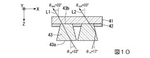
図10は、光制御部材9における透過光L1および反射光L2の光路のシミュレーションを行った結果を示す模式図である。
図10に示すように、透過光L1を想定すると、光拡散部43の光入射端面43aに対して入射角θin=33°で入射した光L1は、側面43cで反射することなく、光射出端面43bを経て、基材41の上面から射出角θout=33°で射出される。一方、反射光L2を想定すると、光拡散部43の光入射端面43aに対して入射角θin=17°で入射した光L2は、側面43cで反射した後、基材41の上面から射出角θout=33°で射出される。このシミュレーションにおいて、光拡散部43のテーパ角(光入射端面43aと側面43cとのなす角度)を85°に設定し、光拡散部43の屈折率を1.6に設定した。なお、基材41は平行平板であり、光は基材41に入射する際の屈折角の分だけ基材41から射出する際に屈折することで相殺され、進行方向が変わらない。そのため、基材41の屈折率は不問とした。
FIG. 10 is a schematic diagram showing a result of a simulation of the optical paths of the transmitted light L1 and the reflected light L2 in the light control member 9.
As shown in FIG. 10, when the transmitted light L1 is assumed, the light L1 incident at an incident angle θin = 33 ° with respect to the light incident end surface 43a of the light diffusing portion 43 is not reflected by the side surface 43c, but is emitted from the light emitting end surface. After passing through 43b, the light is emitted from the upper surface of the base material 41 at an emission angle θout = 33 °. On the other hand, assuming the reflected light L2, the light L2 incident at an incident angle θin = 17 ° with respect to the light incident end surface 43a of the light diffusing portion 43 is reflected by the side surface 43c and then emerges from the upper surface of the base material 41 from the upper surface 41 = 33 ° injection. In this simulation, the taper angle (angle formed between the light incident end face 43a and the side face 43c) of the light diffusion portion 43 was set to 85 °, and the refractive index of the light diffusion portion 43 was set to 1.6. The base material 41 is a parallel plate, and light is offset by being refracted when it is emitted from the base material 41 by the amount of the refraction angle when entering the base material 41, and the traveling direction is not changed. Therefore, the refractive index of the base material 41 is not questioned.

図10のシミュレーション結果を考慮すると、液晶パネル2から射出された光のうち、入射角33°で光制御部材9の光拡散部43に入射する光が多い程、視野角特性が低下する。すなわち、相対的に小さい入射角で光制御部材9に入射する光は、液晶パネル2を法線方向に近い角度で透過してきた光であるため、視野角特性に優れている。その一方、入射角33°というように、相対的に大きい入射角で光制御部材9に入射する光は、液晶パネル2を法線方向から傾いた角度で透過してきた光であるため、視野角特性に劣る。したがって、光制御部材9から射出される光全体としてみると、相対的に大きい入射角で光制御部材9に入射する光が多い程、視野角特性が低下する。   Considering the simulation result of FIG. 10, among the light emitted from the liquid crystal panel 2, the more the light incident on the light diffusion portion 43 of the light control member 9 at an incident angle of 33 °, the lower the viewing angle characteristic. That is, the light incident on the light control member 9 at a relatively small incident angle is light that has been transmitted through the liquid crystal panel 2 at an angle close to the normal direction, and thus has excellent viewing angle characteristics. On the other hand, the light incident on the light control member 9 at a relatively large incident angle such as an incident angle of 33 ° is light that has been transmitted through the liquid crystal panel 2 at an angle inclined from the normal direction. Inferior in characteristics. Accordingly, when the light emitted from the light control member 9 is viewed as a whole, the viewing angle characteristic decreases as the amount of light incident on the light control member 9 with a relatively large incident angle increases.

図11は、バックライト8からの射出光の光束分布を示す図である。図11の横軸は極角[°]であり、縦軸は光束[相対値]である。
本発明者らは、上記の知見に基づき、バックライト8から射出される光のうち、水平方向において広角側に射出される一部の光を狭角側に集光し、正面輝度を上げることにより、視野角特性を改善できると考えた。具体的には、本発明者らは、図11に示すように、破線で示す従来の光束分布に対して、極角33°付近に射出される光を減らし、極角17°付近に射出される光を増やすことにより、液晶パネル2を法線方向に近い角度で透過した光を光制御部材9で拡散させることができ、視野角特性を向上できると考えた。
FIG. 11 is a diagram showing a light flux distribution of light emitted from the backlight 8. The horizontal axis in FIG. 11 is the polar angle [°], and the vertical axis is the luminous flux [relative value].
Based on the above knowledge, the present inventors collect a part of the light emitted from the backlight 8 toward the wide angle side in the horizontal direction to the narrow angle side to increase the front luminance. It was thought that the viewing angle characteristics could be improved. Specifically, as shown in FIG. 11, the present inventors reduced the light emitted near a polar angle of 33 ° and emitted it near a polar angle of 17 ° with respect to the conventional light flux distribution indicated by a broken line. By increasing the amount of light, it was considered that the light transmitted through the liquid crystal panel 2 at an angle close to the normal direction can be diffused by the light control member 9 and the viewing angle characteristics can be improved.

そこで、本発明者らは、バックライト8に用いる集光部材37による集光効果のシミュレーションを行った。以下、シミュレーションの結果について説明する。
図12は、LED35から射出される光の配光分布を示す図である。図13は、集光部材37から射出される光の配光分布を示す図である。
Therefore, the present inventors performed a simulation of the light collecting effect by the light collecting member 37 used in the backlight 8. Hereinafter, the results of the simulation will be described.
FIG. 12 is a diagram showing a light distribution of light emitted from the LED 35. FIG. 13 is a diagram illustrating a light distribution of light emitted from the light collecting member 37.

図12に示すように、LED35から射出された光L0は、極角0°から60°程度までの広い範囲のランバート型の配光分布を有する。これに対して、図13に示すように、LED35から射出された光LSは、集光部材37を透過する。LED35から射出された光L0のうち、相対的に大きい入射角で集光部材37に入射した光は、傾斜面37cで反射し、光の進行方向が光入射端面37aの法線方向に近くなる側に変化する。このように、LED35の光射出側に集光部材37が設けられることによって、LED35から広角方向に射出される光を狭角方向に集光することができる。   As shown in FIG. 12, the light L0 emitted from the LED 35 has a wide Lambertian distribution of light from a polar angle of about 0 ° to about 60 °. On the other hand, as shown in FIG. 13, the light LS emitted from the LED 35 passes through the light collecting member 37. Of the light L0 emitted from the LED 35, the light incident on the light collecting member 37 at a relatively large incident angle is reflected by the inclined surface 37c, and the traveling direction of the light is close to the normal direction of the light incident end surface 37a. Change to the side. Thus, by providing the condensing member 37 on the light emitting side of the LED 35, the light emitted from the LED 35 in the wide angle direction can be condensed in the narrow angle direction.

図14は、LED35および集光部材37からの射出光の極角と輝度比との関係を示すグラフである。
図14の横軸は極角[°]を示し、縦軸は輝度比[−]である。輝度比は、LED35から極角0°方向に射出される光の輝度を1としたときの輝度の比である。
破線のグラフAは、LED35からの射出光の輝度比分布を示す。実線のグラフBは、画面水平方向(方位角0°−180°方向)に沿う集光部材37からの射出光の輝度比分布を示す。1点鎖線のグラフCは、画面垂直方向(方位角90°−270°方向)に沿う集光部材37からの射出光の輝度比分布を示す。
FIG. 14 is a graph showing the relationship between the polar angle of the light emitted from the LED 35 and the light collecting member 37 and the luminance ratio.
In FIG. 14, the horizontal axis represents the polar angle [°], and the vertical axis represents the luminance ratio [−]. The luminance ratio is a luminance ratio when the luminance of light emitted from the LED 35 in the polar angle 0 ° direction is 1.
A broken line graph A shows a luminance ratio distribution of light emitted from the LED 35. A solid line graph B shows the luminance ratio distribution of the emitted light from the light collecting member 37 along the horizontal direction of the screen (azimuth angle 0 ° -180 ° direction). A dashed-dotted line graph C shows the luminance ratio distribution of the light emitted from the light collecting member 37 along the vertical direction of the screen (azimuth angle 90 ° -270 ° direction).

図14に示すように、集光部材37からの射出光は、画面水平方向、画面垂直方向のいずれにおいても、LED35からの射出光に比べて、極角33°付近の輝度比が大きく低下している。したがって、LED35からの射出光は、集光部材37を透過することにより、極角0°方向(正面方向)に集光されることがわかった。   As shown in FIG. 14, the light emitted from the light condensing member 37 has a greatly reduced luminance ratio in the vicinity of a polar angle of 33 °, compared to the light emitted from the LED 35 in both the horizontal and vertical directions of the screen. ing. Therefore, it was found that the light emitted from the LED 35 is condensed in the polar angle 0 ° direction (front direction) by passing through the light collecting member 37.

上述したように、本実施形態の液晶表示装置1によれば、バックライト8の複数のLED35の各々に対応して集光部材37が設けられたことにより、個々のLED35から広角方向に射出された光が集光部材37により狭角方向(正面方向)に集光される。そのため、バックライト8から射出された光が液晶パネル2を透過し、光制御部材9に入射する際に、視野角特性が悪い光の割合が減り、全体として視野角特性を向上することができる。これにより、画像歪みが少なく、色再現性および視野角特性に優れた液晶表示装置1を実現することができる。   As described above, according to the liquid crystal display device 1 of the present embodiment, the condensing member 37 is provided corresponding to each of the plurality of LEDs 35 of the backlight 8, so that each LED 35 emits light in the wide-angle direction. The collected light is collected in a narrow angle direction (front direction) by the light collecting member 37. Therefore, when the light emitted from the backlight 8 passes through the liquid crystal panel 2 and enters the light control member 9, the proportion of light with poor viewing angle characteristics is reduced, and the viewing angle characteristics can be improved as a whole. . Thereby, the liquid crystal display device 1 with little image distortion and excellent color reproducibility and viewing angle characteristics can be realized.

本実施形態の液晶表示装置1においては、直下型のバックライト8が用いられ、さらにLED35からの射出光が集光部材37によって集光されているため、画面内での明るさムラが生じやすい、という課題を有している。この課題に対しては、隣り合うLED35間の距離を短くする、もしくはLED35から拡散板38までの距離を長くすることにより対応が可能である。   In the liquid crystal display device 1 of the present embodiment, the direct type backlight 8 is used, and the light emitted from the LED 35 is collected by the light collecting member 37, so that uneven brightness within the screen is likely to occur. , Has the problem of. This problem can be addressed by shortening the distance between the adjacent LEDs 35 or increasing the distance from the LED 35 to the diffusion plate 38.

図1に示すように、複数のLED35が略等間隔に配置されていることを前提とし、隣り合うLED35間の距離をRとし、LED35と拡散板38との間の距離をDとする。上記の課題を解決するためには、隣り合うLED35間の距離Rは、LED35と拡散板38との間の距離Dよりも小さいことが少なくとも望ましい。すなわち、本実施形態のバックライト8は、R/D<1の条件を満たすことが少なくとも望ましい。   As shown in FIG. 1, assuming that the plurality of LEDs 35 are arranged at substantially equal intervals, the distance between adjacent LEDs 35 is R, and the distance between the LED 35 and the diffusion plate 38 is D. In order to solve the above problem, it is preferable that the distance R between the adjacent LEDs 35 is at least smaller than the distance D between the LED 35 and the diffusion plate 38. That is, it is at least desirable that the backlight 8 of the present embodiment satisfies the condition of R / D <1.

さらに、本発明者らは、隣り合うLED35間の距離とLED35から拡散板38までの距離との比について検討した。
R/Dの値として、最初に、現状の直下型バックライトの一例であるR/D=3.3について検討した。R/D=3.3とした場合、本実施形態のバックライト8は集光部材37を備えているため、本実施形態のバックライト8による輝度ムラは、現状の一般的な直下型バックライトの輝度ムラよりも大きくなる。
Furthermore, the present inventors examined the ratio between the distance between adjacent LEDs 35 and the distance from the LED 35 to the diffusion plate 38.
As the value of R / D, first, R / D = 3.3, which is an example of the current direct type backlight, was examined. When R / D = 3.3, the backlight 8 of the present embodiment includes the light collecting member 37. Therefore, the luminance unevenness due to the backlight 8 of the present embodiment is the current general direct type backlight. It becomes larger than the luminance unevenness.

次に、R/D<1の範囲を満たす種々のR/Dの値について検討した。その結果、R/D≦0.7の範囲内でR/Dの値を設定することにより、本実施形態のバックライト8による輝度ムラは、現状の一般的な直下型バックライトの輝度ムラと同等以下となることが確認された。さらに、集光部材37からの射出光を拡散板38、プリズムシート等の光学シート群39を通すことにより、液晶パネル2に入射する時点の明暗の差をさらに小さくすることができる。すなわち、本実施形態のバックライト8は、R/D≦0.7の条件を満たすことがさらに望ましい。   Next, various R / D values satisfying the range of R / D <1 were examined. As a result, by setting the value of R / D within the range of R / D ≦ 0.7, the luminance unevenness due to the backlight 8 of the present embodiment is the luminance unevenness of the current general direct type backlight. It was confirmed that it was equivalent or less. Further, by passing the light emitted from the light condensing member 37 through the optical sheet group 39 such as the diffusion plate 38 and the prism sheet, the difference in brightness when entering the liquid crystal panel 2 can be further reduced. That is, it is further desirable that the backlight 8 of the present embodiment satisfies the condition of R / D ≦ 0.7.

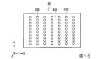
また、本実施形態のバックライト8は、複数の集光部材37の光射出側に位置する拡散板38をさらに備えている。図15は、拡散板38の平面図である。
図15に示すように、拡散板38は、基材381と、基材381の内部に分散された複数の拡散材382と、を備えている。複数の拡散材382の配置密度は、画面水平方向と画面垂直方向とで異なる。具体的には、画面水平方向における拡散材382の配置密度は、画面垂直方向における拡散材382の配置密度よりも小さい。そのため、拡散板38は、画面水平方向と画面垂直方向とで光の拡散性に異方性を有する。画面水平方向における光の拡散性は、画面垂直方向における光の拡散性よりも小さい。これにより、拡散板38における光の拡散性が大きい方向は、光制御部材9の遮光部42の長軸方向と平行になる。
Further, the backlight 8 of the present embodiment further includes a diffusion plate 38 positioned on the light exit side of the plurality of light collecting members 37. FIG. 15 is a plan view of the diffusion plate 38.
As shown in FIG. 15, the diffusion plate 38 includes a base material 381 and a plurality of diffusion materials 382 dispersed inside the base material 381. The arrangement density of the plurality of diffusion materials 382 differs between the horizontal direction of the screen and the vertical direction of the screen. Specifically, the arrangement density of the diffusion material 382 in the horizontal direction of the screen is smaller than the arrangement density of the diffusion material 382 in the vertical direction of the screen. Therefore, the diffusion plate 38 has anisotropy in light diffusibility in the horizontal direction and the vertical direction of the screen. The light diffusibility in the horizontal direction of the screen is smaller than the light diffusibility in the vertical direction of the screen. Thereby, the direction in which the light diffusibility in the diffusion plate 38 is large is parallel to the major axis direction of the light shielding portion 42 of the light control member 9.

本実施形態の液晶表示装置1においては、バックライト8が集光部材37を備えたことにより、バックライト8からの射出光を少なくとも画面水平方向に集光させている。そのため、上述したように、拡散板38は、画面水平方向における光の拡散性が画面垂直方向における光の拡散性よりも小さいことが好ましい。これにより、液晶表示装置1の視野角特性を効果的に改善しつつ、画面内の明るさムラを低減することができる。   In the liquid crystal display device 1 of the present embodiment, the backlight 8 includes the light collecting member 37, so that the light emitted from the backlight 8 is condensed at least in the horizontal direction of the screen. Therefore, as described above, the diffusing plate 38 preferably has a light diffusibility in the horizontal direction of the screen smaller than that in the vertical direction of the screen. Thereby, the brightness unevenness in a screen can be reduced, improving the viewing angle characteristic of the liquid crystal display device 1 effectively.

本実施形態の液晶表示装置1に用いられる拡散板は、拡散異方性を有するものであればよく、拡散異方性を付与する手段として、複数の拡散材の配置密度が画面水平方向と画面垂直方向とで異なる形態の図15の拡散板38に限られるものではない。
例えば、以下の第1〜第3変形例の拡散板が用いられてもよい。
The diffusion plate used in the liquid crystal display device 1 of the present embodiment only needs to have diffusion anisotropy. As a means for imparting diffusion anisotropy, the arrangement density of a plurality of diffusion materials is set in the horizontal direction of the screen and the screen. It is not restricted to the diffuser plate 38 of FIG. 15 which is different in the vertical direction.
For example, the diffusion plates of the following first to third modifications may be used.

図16Aは、第1変形例の拡散板56の画面垂直方向における断面図である。図16Bは、第1変形例の拡散板56の画面水平方向における断面図である。
図16Aおよび図16Bに示すように、拡散板56は、基材561と、楕円球状の複数の拡散材562と、を備える。複数の拡散材562は、個々の拡散材562の画面垂直方向(Y軸方向)の断面形状が円形となり、画面水平方向(X軸方向)の断面形状が楕円形となるように配向している。
FIG. 16A is a cross-sectional view in the screen vertical direction of the diffusion plate 56 of the first modification. FIG. 16B is a cross-sectional view in the horizontal direction of the screen of the diffusion plate 56 of the first modification.
As shown in FIGS. 16A and 16B, the diffusion plate 56 includes a base material 561 and a plurality of elliptical diffusing materials 562. The plurality of diffusing materials 562 are oriented so that the cross-sectional shape in the screen vertical direction (Y-axis direction) of each diffusing material 562 is circular and the cross-sectional shape in the horizontal screen direction (X-axis direction) is elliptical. .

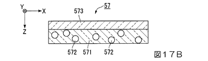
図17Aは、第2変形例の拡散板57の画面垂直方向における断面図である。図17Bは、第2変形例の拡散板57の画面水平方向における断面図である。
図17Aおよび図17Bに示すように、拡散板57は、基材571と、球状の複数の拡散材572と、複数のプリズム構造体573と、を備える。複数のプリズム構造体573は、三角柱状のプリズム構造体573が画面水平方向(X軸方向)に延在し、画面垂直方向(Y軸方向)に複数並ぶように形成されている。
FIG. 17A is a cross-sectional view of the diffusion plate 57 of the second modified example in the screen vertical direction. FIG. 17B is a cross-sectional view of the diffusion plate 57 of the second modified example in the horizontal direction of the screen.
As illustrated in FIGS. 17A and 17B, the diffusion plate 57 includes a base material 571, a plurality of spherical diffusion materials 572, and a plurality of prism structures 573. The plurality of prism structures 573 are formed so that a prismatic prism structure 573 extends in the horizontal direction of the screen (X-axis direction) and is arranged in the vertical direction of the screen (Y-axis direction).

図18Aは、第3変形例の拡散板58の画面垂直方向における断面図である。図18Bは、第3変形例の拡散板58の画面水平方向における断面図である。
図18Aおよび図18Bに示すように、拡散板58は、基材581と、複数の凸状体582と、を備える。複数の凸状体582は、各凸状体582の長手方向が画面水平方向(X軸方向)に略一致し、各凸状体582の短手方向が画面垂直方向(Y軸方向)に略一致するように形成されている。この種の拡散板58として、例えば王子製紙社製のナノバックリングシートを用いることができる。
FIG. 18A is a cross-sectional view of the diffusion plate 58 of the third modified example in the screen vertical direction. FIG. 18B is a cross-sectional view of the diffusion plate 58 of the third modification in the horizontal direction of the screen.
As shown in FIGS. 18A and 18B, the diffusion plate 58 includes a base material 581 and a plurality of convex bodies 582. In the plurality of convex bodies 582, the longitudinal direction of each convex body 582 is substantially coincident with the horizontal direction of the screen (X-axis direction), and the short direction of each convex body 582 is substantially parallel to the screen vertical direction (Y-axis direction). It is formed to match. As this type of diffusion plate 58, for example, a nano buckling sheet manufactured by Oji Paper Co., Ltd. can be used.

[第2実施形態]
以下、本発明の第2実施形態について、図19〜図22を用いて説明する。
第2実施形態の液晶表示装置の基本構成は第1実施形態と同一であり、集光部材の構成が第1実施形態と異なる。そのため、第2実施形態では、集光部材についてのみ説明する。
図19は、第2実施形態の液晶表示装置に用いる集光部材の断面図である。
図19〜図22において、第1実施形態で用いた図面と共通の構成要素には同一の符号を付し、説明を省略する。
[Second Embodiment]
Hereinafter, a second embodiment of the present invention will be described with reference to FIGS.
The basic configuration of the liquid crystal display device of the second embodiment is the same as that of the first embodiment, and the configuration of the light collecting member is different from that of the first embodiment. Therefore, in 2nd Embodiment, only a condensing member is demonstrated.
FIG. 19 is a cross-sectional view of a light collecting member used in the liquid crystal display device of the second embodiment.
19 to 22, the same components as those used in the first embodiment are denoted by the same reference numerals, and description thereof is omitted.

図20は、第1実施形態の集光部材37からの射出光の配光分布を示す図である。
図20に示すように、第1実施形態の集光部材37において、光入射端面37aは、平坦な面であり、LED35の光射出面35aに平行な面である。この場合、LED35から射出された光のうち、相対的に大きい射出角で射出された一部の光L5は、光入射端面に対して大きい入射角で入射する。そのため、光L5は、光入射端面37aで反射し、集光部材37の内部に入射することができない。光L5は液晶パネル2に入射せず、表示に寄与しないため、光利用効率を低下させる原因となる。
FIG. 20 is a diagram illustrating a light distribution of emitted light from the light collecting member 37 according to the first embodiment.
As shown in FIG. 20, in the light collecting member 37 of the first embodiment, the light incident end surface 37 a is a flat surface and is a surface parallel to the light emitting surface 35 a of the LED 35. In this case, of the light emitted from the LED 35, a part of the light L5 emitted at a relatively large emission angle is incident on the light incident end surface at a large incident angle. Therefore, the light L <b> 5 is reflected by the light incident end surface 37 a and cannot enter the light collecting member 37. Since the light L5 does not enter the liquid crystal panel 2 and does not contribute to display, it causes a reduction in light use efficiency.

これに対して、図19に示すように、第2実施形態の集光部材62の光入射端面62aには、内面がなだらかに湾曲した凹部63が設けられている。また、集光部材62の光軸C方向から見て、凹部63の平面形状は円形である。凹部63の平面形状をなす円の中心は、光入射端面62a全体の平面形状をなす円の中心に一致している。この構成により、光入射端面62aは、全体が曲面状の凹面となっている。
その他の構成は第1実施形態と同様である。
On the other hand, as shown in FIG. 19, the light incident end surface 62a of the light collecting member 62 of the second embodiment is provided with a concave portion 63 whose inner surface is gently curved. Further, when viewed from the direction of the optical axis C of the light collecting member 62, the planar shape of the recess 63 is circular. The center of the circle forming the planar shape of the recess 63 coincides with the center of the circle forming the planar shape of the entire light incident end surface 62a. With this configuration, the entire light incident end face 62a is a curved concave surface.
Other configurations are the same as those of the first embodiment.

本実施形態の構成によれば、第1実施形態の集光部材37において表示に寄与できない光L5と同じ射出角で射出された光L6についても、光入射端面62aが凹面となっていることにより、光入射端面62aに対する入射角が第1実施形態の光入射端面37aに対する入射角よりも小さくなる。その結果、光L6は、光入射端面62aから集光部材62の内部に入射する。これにより、光L6は液晶パネル2に入射し、表示に寄与できるため、第1実施形態に比べて光利用効率を高めることができる。   According to the configuration of the present embodiment, the light incident end face 62a is also concave for the light L6 emitted at the same emission angle as the light L5 that cannot contribute to display in the light collecting member 37 of the first embodiment. The incident angle with respect to the light incident end face 62a is smaller than the incident angle with respect to the light incident end face 37a of the first embodiment. As a result, the light L6 enters the condensing member 62 from the light incident end face 62a. Thereby, since the light L6 enters the liquid crystal panel 2 and can contribute to the display, the light use efficiency can be improved as compared with the first embodiment.

集光部材62による集光効果を効果的に得るためには、凹部63の平面形状である円の半径をb(mm)とし、凹部63の最大深さをh(mm)としたとき、凹部63の半径bに対する最大深さhの比h/bは、0<h/b<1であることが望ましい。具体的に、h/bは、0.5程度であることが望ましい。図19では、h/b=0.5としたときの集光部材62からの射出光の配光分布を示している。   In order to effectively obtain the light collecting effect by the light collecting member 62, when the radius of the circle which is the planar shape of the concave portion 63 is b (mm) and the maximum depth of the concave portion 63 is h (mm), the concave portion The ratio h / b of the maximum depth h to the radius b of 63 is preferably 0 <h / b <1. Specifically, h / b is desirably about 0.5. FIG. 19 shows the light distribution of the emitted light from the light collecting member 62 when h / b = 0.5.

図21は、凹部66の半径bに対する最大深さhの比を1(h/b=1)としたときの集光部材65からの射出光の配光分布を示す図である。
図21に示すように、h/b=1とした場合も、LED35から広角側に射出された光が集光部材65の内部に入射するため、光利用効率を高めることができる。ただし、図21に示した集光部材65においては、図19に示したh/b=0.5の集光部材62と比べて、広角に発散する方向に射出される光が僅かに多くなる。したがって、0<h/b<1であることが望ましい。
FIG. 21 is a diagram showing a light distribution of emitted light from the light collecting member 65 when the ratio of the maximum depth h to the radius b of the recess 66 is 1 (h / b = 1).
As shown in FIG. 21, even when h / b = 1, light emitted from the LED 35 to the wide angle side is incident on the inside of the light collecting member 65, so that the light use efficiency can be improved. However, in the light collecting member 65 shown in FIG. 21, the amount of light emitted in the direction of diverging in a wide angle is slightly larger than that of the light collecting member 62 having h / b = 0.5 shown in FIG. . Therefore, it is desirable that 0 <h / b <1.

本実施形態においても、バックライト8が集光部材62,65を備えたことにより、画像歪みが少なく、色再現性および視野角特性に優れた液晶表示装置を実現できる、という第1実施形態と同様の効果が得られる。   Also in the present embodiment, the backlight 8 includes the light collecting members 62 and 65, so that a liquid crystal display device with less image distortion and excellent color reproducibility and viewing angle characteristics can be realized. Similar effects can be obtained.

図22は、本発明者らのシミュレーション結果を示しており、第2実施形態の集光部材62からの射出光の極角と輝度比との関係を示すグラフである。
図22の横軸は極角[°]を示し、縦軸は輝度比[−]である。輝度比は、LED35から極角0°方向に射出される光の輝度を1としたときの輝度の比である。
破線のグラフAは、LED35からの射出光の輝度比分布を示す。実線のグラフBは、画面水平方向(方位角0°−180°方向)に沿う集光部材62からの射出光の輝度比分布を示す。1点鎖線のグラフCは、画面垂直方向(方位角90°−270°方向)に沿う集光部材62からの射出光の輝度比分布を示す。
FIG. 22 shows the simulation results of the present inventors and is a graph showing the relationship between the polar angle of the emitted light from the light collecting member 62 of the second embodiment and the luminance ratio.
In FIG. 22, the horizontal axis indicates the polar angle [°], and the vertical axis indicates the luminance ratio [−]. The luminance ratio is a luminance ratio when the luminance of light emitted from the LED 35 in the polar angle 0 ° direction is 1.
A broken line graph A shows a luminance ratio distribution of light emitted from the LED 35. A solid line graph B shows a luminance ratio distribution of light emitted from the light collecting member 62 along the horizontal direction of the screen (azimuth angle 0 ° -180 ° direction). A dashed-dotted line graph C shows the luminance ratio distribution of the light emitted from the light collecting member 62 along the vertical direction of the screen (azimuth angle 90 ° -270 ° direction).

図22に示すように、集光部材62からの射出光は、画面水平方向、画面垂直方向のいずれにおいても、LED35からの射出光に比べて、極角33°付近の輝度比が大きく低下している。したがって、LED35からの射出光は、集光部材62を透過することにより、極角0°方向(正面方向)に集光されることがわかった。   As shown in FIG. 22, the brightness ratio of the light emitted from the light collecting member 62 is greatly reduced in the vicinity of the polar angle of 33 ° compared to the light emitted from the LED 35 in both the horizontal direction and the vertical direction of the screen. ing. Therefore, it was found that the light emitted from the LED 35 is condensed in the polar angle 0 ° direction (front direction) by passing through the light collecting member 62.

第2実施形態の場合、極角33°での輝度比は、画面垂直方向において0.5程度にまで低減されているのに対し、画面水平方向においては0.3程度にまで低減されている。このように、特に集光状態を改善したい方位角方向である画面水平方向における集光効果が、画面垂直方向における集光効果に比べて大きく、視野角の改善にとって理想的であることがわかった。また、図22に示す第2実施形態のグラフは、図14に示す第1実施形態のグラフのような変曲点を持たず、形状がなだらかであることがわかった。そのため、観察者が極角を変化させながら画面を見たときに明るさの急激な変化が少なく、斜め方向からの表示品位を効果的に高めることができる。   In the case of the second embodiment, the luminance ratio at a polar angle of 33 ° is reduced to about 0.5 in the vertical direction of the screen, but is reduced to about 0.3 in the horizontal direction of the screen. . In this way, it was found that the condensing effect in the horizontal direction of the screen, which is the azimuth angle direction in which the condensing state is to be improved, is larger than the condensing effect in the vertical direction of the screen and is ideal for improving the viewing angle. . Further, it was found that the graph of the second embodiment shown in FIG. 22 does not have an inflection point like the graph of the first embodiment shown in FIG. 14 and has a gentle shape. Therefore, when the observer looks at the screen while changing the polar angle, there is little sudden change in brightness, and the display quality from the oblique direction can be effectively enhanced.

本実施形態では、集光部材62,65の光入射端面62a,65aの全体が曲面状の凹面である例を示した。この構成に代えて、例えば集光部材の光入射端面のうち、中央部は平坦面であり、LEDから広角側に射出される光が入射する一部の領域のみが曲面状の凹面となっていてもよい。   In the present embodiment, an example in which the entire light incident end surfaces 62a and 65a of the light collecting members 62 and 65 are curved concave surfaces is shown. Instead of this configuration, for example, the central portion of the light incident end face of the light collecting member is a flat surface, and only a partial region where light emitted from the LED to the wide angle side is incident is a curved concave surface. May be.

[第3実施形態]
以下、本発明の第3実施形態について、図23〜図24を用いて説明する。
第3実施形態の液晶表示装置の基本構成は第1実施形態と同一であり、集光部材の構成が第1実施形態と異なる。そのため、第3実施形態では、集光部材についてのみ説明する。
図23は、第3実施形態の液晶表示装置に用いる集光部材の断面図である。
図23〜図24において、第1実施形態で用いた図面と共通の構成要素には同一の符号を付し、説明を省略する。
[Third Embodiment]
Hereinafter, a third embodiment of the present invention will be described with reference to FIGS.
The basic configuration of the liquid crystal display device of the third embodiment is the same as that of the first embodiment, and the configuration of the light collecting member is different from that of the first embodiment. Therefore, in 3rd Embodiment, only a condensing member is demonstrated.
FIG. 23 is a cross-sectional view of a light collecting member used in the liquid crystal display device of the third embodiment.
23 to 24, the same reference numerals are given to the same components as those used in the first embodiment, and the description thereof will be omitted.

第1実施形態の集光部材37の傾斜面37cは、位置によらずに傾斜角が一定であった。これに対して、図23に示すように、第3実施形態の集光部材71の傾斜面71cは、傾斜角が光入射端面71aから光射出端面71bに向けて順次大きくなる方向に変化している。すなわち、集光部材37の光軸Cを含む平面で切断した断面で見ると、傾斜面71cの断面形状は、内側に凸となるように湾曲した曲線状である。   The inclined surface 37c of the light collecting member 37 of the first embodiment has a constant inclination angle regardless of the position. On the other hand, as shown in FIG. 23, the inclined surface 71c of the condensing member 71 of the third embodiment changes in a direction in which the inclination angle increases sequentially from the light incident end surface 71a to the light emitting end surface 71b. Yes. That is, when viewed in a cross section cut by a plane including the optical axis C of the light collecting member 37, the cross-sectional shape of the inclined surface 71c is a curved shape curved so as to be convex inward.

傾斜面71c上の1点を通る接線S1,S2と光軸Cに平行な直線Vとのなす角度を傾斜面71cの傾斜角αと定義する。このとき、傾斜面71cが光入射端面71aと接する角部での傾斜面71cの傾斜角α1は、例えば6°である。傾斜面71cが光射出端面71bと接する角部での傾斜角α2は、例えば12°である。このように、傾斜面71cの傾斜角αは光入射端面71a側から光射出端面71b側に向けて、6°から12°に増加している。
その他の構成は第1実施形態と同様である。
An angle formed between tangents S1 and S2 passing through one point on the inclined surface 71c and a straight line V parallel to the optical axis C is defined as an inclination angle α of the inclined surface 71c. At this time, the inclination angle α1 of the inclined surface 71c at the corner where the inclined surface 71c contacts the light incident end surface 71a is, for example, 6 °. The inclination angle α2 at the corner where the inclined surface 71c is in contact with the light emitting end surface 71b is, for example, 12 °. Thus, the inclination angle α of the inclined surface 71c increases from 6 ° to 12 ° from the light incident end surface 71a side toward the light emitting end surface 71b side.
Other configurations are the same as those of the first embodiment.

上述したように、集光部材71は、LED35から種々の方向に射出される光のうち、極角33°付近に射出される光を減らし、極角17°付近に射出される光を増やすことが望ましい。そのためには、本実施形態のように、傾斜面71cの傾斜角αを一定にするのではなく、適宜変化させることにより、射出光の配光分布を制御することが有効である。具体的には、傾斜面71cの傾斜角αを6°〜12°の範囲内で変化させることにより、極角33°付近に射出される光を減らし、極角17°付近に射出される光を増やすことができる。   As described above, the condensing member 71 reduces the light emitted near the polar angle 33 ° out of the light emitted from the LEDs 35 in various directions, and increases the light emitted near the polar angle 17 °. Is desirable. For this purpose, it is effective to control the light distribution of the emitted light by appropriately changing the inclination angle α of the inclined surface 71c as in the present embodiment, instead of making it constant. Specifically, by changing the inclination angle α of the inclined surface 71c within the range of 6 ° to 12 °, the light emitted near the polar angle 33 ° is reduced and the light emitted near the polar angle 17 ° Can be increased.

本実施形態においても、バックライト8が集光部材71を備えたことにより、画像歪みが少なく、色再現性および視野角特性に優れた液晶表示装置を実現できる、という第1実施形態と同様の効果が得られる。   Also in this embodiment, since the backlight 8 includes the light collecting member 71, it is possible to realize a liquid crystal display device with less image distortion and excellent color reproducibility and viewing angle characteristics, as in the first embodiment. An effect is obtained.

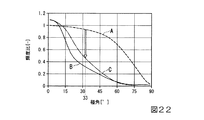
図24は、本発明者らのシミュレーション結果を示しており、第3実施形態の集光部材71からの射出光の極角と輝度比との関係を示すグラフである。
図24の横軸は極角[°]を示し、縦軸は輝度比[−]である。輝度比は、LED35から極角0°方向に射出される光の輝度を1としたときの輝度の比である。
破線のグラフAは、LED35からの射出光の輝度比分布を示す。実線のグラフBは、画面水平方向(方位角0°−180°方向)に沿う集光部材71からの射出光の輝度比分布を示す。
FIG. 24 shows the simulation results of the present inventors and is a graph showing the relationship between the polar angle of the emitted light from the condensing member 71 of the third embodiment and the luminance ratio.
In FIG. 24, the horizontal axis indicates the polar angle [°], and the vertical axis indicates the luminance ratio [−]. The luminance ratio is a luminance ratio when the luminance of light emitted from the LED 35 in the polar angle 0 ° direction is 1.
A broken line graph A shows a luminance ratio distribution of light emitted from the LED 35. A solid line graph B shows the luminance ratio distribution of the light emitted from the light collecting member 71 along the horizontal direction of the screen (azimuth angle 0 ° -180 ° direction).

図24に示すように、集光部材71からの射出光は、LED単品での射出光と比較して、極角25°付近よりも広角側の輝度比が大きく低下している。例えば極角33°での輝度比を見ると、0.9程度から0.3程度まで大きく低下している。また、集光部材71からの射出光は、LED単品での射出光に対して、極角25°よりも狭角側の輝度比が上昇している。例えば極角17°での輝度比を見ると、1.2を超える値にまで上昇している。このように、本実施形態の集光部材71によれば、液晶表示装置の視野角特性が大きく改善される見通しが得られた。   As shown in FIG. 24, the light emitted from the light condensing member 71 has a brightness ratio on the wide-angle side that is significantly lower than the vicinity of the polar angle of 25 ° as compared with the light emitted from the single LED. For example, when looking at the luminance ratio at a polar angle of 33 °, it is greatly reduced from about 0.9 to about 0.3. In addition, the light emitted from the light collecting member 71 has a brightness ratio on the narrower angle side than the polar angle of 25 ° with respect to the light emitted from the single LED. For example, looking at the luminance ratio at a polar angle of 17 °, it rises to a value exceeding 1.2. Thus, according to the condensing member 71 of this embodiment, the view angle characteristic of a liquid crystal display device is expected to be greatly improved.

[第4実施形態]
上述の第1実施形態〜第3実施形態の液晶表示装置は、各種電子機器に適用することができる。
以下、上述の第1実施形態〜第3実施形態の液晶表示装置1を備えた電子機器について、図25〜図27を用いて説明する。
[Fourth Embodiment]
The liquid crystal display devices of the first to third embodiments described above can be applied to various electronic devices.
Hereinafter, an electronic apparatus provided with the liquid crystal display device 1 of the first to third embodiments will be described with reference to FIGS.

上述の第1実施形態〜第3実施形態の液晶表示装置1は、例えば、図25に示す薄型テレビ250に適用できる。
図25に示すように、薄型テレビ250は、表示部251、スピーカ252、キャビネット253およびスタンド254等を備えている。
表示部251として、上述の第1実施形態〜第3実施形態の液晶表示装置1を好適に適用できる。上述の第1実施形態〜第3実施形態の液晶表示装置1を薄型テレビ250の表示部251に適用することにより、視野角特性に優れた映像を表示することができる。
The liquid crystal display device 1 according to the first to third embodiments described above can be applied to, for example, a thin television 250 shown in FIG.
As shown in FIG. 25, the flat-screen television 250 includes a display unit 251, a speaker 252, a cabinet 253, a stand 254, and the like.
As the display unit 251, the liquid crystal display device 1 of the first to third embodiments described above can be suitably applied. By applying the liquid crystal display device 1 of the first to third embodiments described above to the display unit 251 of the thin television 250, it is possible to display an image with excellent viewing angle characteristics.

上述の第1実施形態〜第3実施形態の液晶表示装置1は、例えば、図26に示すスマートフォン240に適用できる。
図26に示すように、スマートフォン240は、音声入力部241、音声出力部242、操作スイッチ244、表示部245、タッチパネル243および筐体246等を備えている。
表示部245として、上述の第1実施形態〜第3実施形態の液晶表示装置1を好適に適用できる。上述の第1実施形態〜第3実施形態の液晶表示装置1をスマートフォン240の表示部245に適用することによって、視野角特性に優れた映像を表示することができる。
The liquid crystal display device 1 of the first to third embodiments described above can be applied to, for example, the smartphone 240 shown in FIG.
As shown in FIG. 26, the smartphone 240 includes a voice input unit 241, a voice output unit 242, an operation switch 244, a display unit 245, a touch panel 243, a housing 246, and the like.
As the display unit 245, the liquid crystal display device 1 of the above-described first to third embodiments can be suitably applied. By applying the liquid crystal display device 1 of the first to third embodiments described above to the display unit 245 of the smartphone 240, an image with excellent viewing angle characteristics can be displayed.

上述の第1実施形態〜第3実施形態の液晶表示装置1は、例えば、図27に示すノートパソコン270に適用できる。
図27に示すように、ノートパソコン270は、表示部271、キーボード272、タッチパッド273、メインスイッチ274、カメラ275、記録媒体スロット276および筐体277等を備えている。
表示部271として、上述の第1実施形態〜第3実施形態の液晶表示装置1を好適に適用できる。上述の第1実施形態〜第3実施形態の液晶表示装置1をノートパソコン270の表示部271に適用することによって、視野角特性に優れた映像を表示することができる。
The liquid crystal display device 1 of the first to third embodiments described above can be applied to, for example, a notebook computer 270 shown in FIG.
As shown in FIG. 27, the notebook computer 270 includes a display unit 271, a keyboard 272, a touch pad 273, a main switch 274, a camera 275, a recording medium slot 276, a housing 277, and the like.
As the display unit 271, the liquid crystal display device 1 of the first to third embodiments described above can be suitably applied. By applying the liquid crystal display device 1 of the first to third embodiments described above to the display unit 271 of the notebook computer 270, an image having excellent viewing angle characteristics can be displayed.

なお、本発明のいくつかの態様における技術範囲は上記実施形態に限定されるものではなく、本発明の態様における趣旨を逸脱しない範囲において種々の変更を加えることが可能である。
例えば上記実施形態では、集光部材として、PMMA等の光透過性を有する材料から構成された中実の集光部材の例を挙げたが、この構成に代えて、例えば内部が中空の筒体で構成され、筒体の内面が反射面となっている集光部材が用いられてもよい。
The technical scope of some aspects of the present invention is not limited to the above-described embodiment, and various modifications can be made without departing from the spirit of the aspect of the present invention.
For example, in the above-described embodiment, an example of a solid light collecting member made of a light-transmitting material such as PMMA is given as the light collecting member. A condensing member may be used in which the inner surface of the cylinder is a reflecting surface.

また、上記実施形態における光制御部材の基材の視認側に、反射防止構造、偏光フィルター層、帯電防止層、防眩処理層、防汚処理層のうちの少なくとも一つが設けられた構成であってもよい。この構成によれば、基材の視認側に設ける層の種類に応じて、外光反射を低減する機能、塵埃や汚れの付着を防止する機能、傷を防止する機能等を付加することができ、視野角特性の経時劣化を防ぐことができる。   The light control member in the above embodiment has a configuration in which at least one of an antireflection structure, a polarizing filter layer, an antistatic layer, an antiglare treatment layer, and an antifouling treatment layer is provided on the viewing side of the base material. May be. According to this configuration, it is possible to add a function to reduce external light reflection, a function to prevent the adhesion of dust and dirt, a function to prevent scratches, and the like according to the type of layer provided on the viewing side of the substrate. Further, it is possible to prevent deterioration of viewing angle characteristics with time.

特に、反射防止構造の一例として、光制御部材の基材の視認側にアンチグレア層が設けられた構成であってもよい。アンチグレア層としては、例えば、光の干渉を用いて外光を打ち消す誘電体多層膜等が用いられる。   In particular, as an example of the antireflection structure, a configuration in which an antiglare layer is provided on the viewing side of the base material of the light control member may be used. As the antiglare layer, for example, a dielectric multilayer film that cancels external light using light interference is used.

反射防止構造の他の例として、光制御部材の基材の視認側に、いわゆるモスアイ構造が設けられた構成であってもよい。本発明において、モスアイ構造は、以下の構造や形状を含むものとする。モスアイ構造は、周期が可視光の波長以下の凹凸形状であり、いわゆる“蛾の目(Moth-eye)”構成の原理を利用した形状や構造である。凹凸の周期は、可視光(λ=380nm〜780nm)の波長以下に制御されている。凹凸パターンを構成する凸部の2次元的な大きさは、10nm以上、500nm未満である。基材に入射する光に対する屈折率を凹凸の深さ方向に沿って入射媒体(空気)の屈折率から基材の屈折率まで連続的に変化させることによって反射を抑制する。   As another example of the antireflection structure, a so-called moth-eye structure may be provided on the viewing side of the base material of the light control member. In the present invention, the moth-eye structure includes the following structures and shapes. The moth-eye structure is a concavo-convex shape with a period equal to or less than the wavelength of visible light, and is a shape or structure using the principle of a so-called “Moth-eye” configuration. The period of the unevenness is controlled to be equal to or less than the wavelength of visible light (λ = 380 nm to 780 nm). The two-dimensional size of the convex portions constituting the concavo-convex pattern is 10 nm or more and less than 500 nm. Reflection is suppressed by continuously changing the refractive index for light incident on the base material from the refractive index of the incident medium (air) to the refractive index of the base material along the depth direction of the unevenness.

また、液晶表示装置内の4つのドメインについては、各々のドメインの面積が異なっていてもよいし、液晶分子のダイレクタの方向は完全に90°ずつ異なっていなくてもよい。また、本発明は、1つの画素内に少なくとも2つのドメインがある場合に適用されるものであり、3つ以上のドメインがあってもよい。その場合、視野角特性を改善したい方位角方向に合わせて、光制御部材の遮光層の長軸方向、短軸方向、および集光部材の光射出端面の長軸方向、短軸方向を配置すればよい。   Further, the four domains in the liquid crystal display device may have different areas, and the director directions of the liquid crystal molecules may not be completely different from each other by 90 °. The present invention is applied when there are at least two domains in one pixel, and there may be three or more domains. In that case, the major axis direction and minor axis direction of the light shielding layer of the light control member and the major axis direction and minor axis direction of the light emission end face of the light collecting member are arranged in accordance with the azimuth direction in which the viewing angle characteristics are desired to be improved. That's fine.

また、上記実施形態においては、図28Aに示すように、液晶パネル2の1個の画素PXが長方形状の赤(R)、緑(G)、青(B)の3個の副画素で構成され、これら3個の副画素が画面の垂直方向(矢印V方向)に長辺方向を向けて水平方向(矢印H方向)に配列されている例を示した。副画素の配置は、この例に限ることはない。例えば図28Bに示すように、R,G,Bの3個の副画素が画面の水平方向(矢印H方向)に長辺方向を向けて垂直方向(矢印V方向)に配列されていてもよい。   Further, in the above embodiment, as shown in FIG. 28A, one pixel PX of the liquid crystal panel 2 is configured by three rectangular subpixels of red (R), green (G), and blue (B). In the example, these three subpixels are arranged in the horizontal direction (arrow H direction) with the long side direction directed in the vertical direction (arrow V direction) of the screen. The arrangement of subpixels is not limited to this example. For example, as shown in FIG. 28B, three subpixels R, G, and B may be arranged in the vertical direction (arrow V direction) with the long side direction directed in the horizontal direction (arrow H direction) of the screen. .

また、図28Cに示すように、液晶パネル2の1個の画素が長方形状の赤(R)、緑(G)、青(B)、黄(Y)の4個の副画素で構成され、これら4個の副画素が画面の垂直方向(矢印V方向)に長辺方向を向けて水平方向(矢印H方向)に配列されていてもよい。
もしくは、図28Dに示すように、R,G,B,Yの4個の副画素が画面の水平方向(矢印H方向)に長辺方向を向けて垂直方向(矢印V方向)に配列されていてもよい。
もしくは、図28Eに示すように、液晶パネルの1個の画素が正方形状のR,G,B,Yの4個の副画素で構成され、画面の水平方向と垂直方向とに2行2列に配置されていてもよい。
Further, as shown in FIG. 28C, one pixel of the liquid crystal panel 2 is composed of four rectangular sub-pixels of red (R), green (G), blue (B), and yellow (Y), These four subpixels may be arranged in the horizontal direction (arrow H direction) with the long side direction directed in the vertical direction (arrow V direction) of the screen.
Alternatively, as shown in FIG. 28D, four sub-pixels R, G, B, and Y are arranged in the vertical direction (arrow V direction) with the long side direction directed in the horizontal direction (arrow H direction) of the screen. May be.
Or, as shown in FIG. 28E, one pixel of the liquid crystal panel is composed of four square subpixels R, G, B, and Y, and two rows and two columns in the horizontal and vertical directions of the screen. May be arranged.

その他、液晶表示装置および光制御部材の各構成部材の材料、数、配置等に関する具体的な構成は上記実施形態に限ることなく、適宜変更が可能である。例えば上記実施形態では、液晶パネルの外側に偏光板や位相差板を配置する例を示したが、この構成に代えて、液晶パネルを構成する一対の基板の内側に偏光層や位相差層を形成しても良い。   In addition, the specific configuration regarding the material, the number, the arrangement, and the like of each constituent member of the liquid crystal display device and the light control member is not limited to the above-described embodiment, and can be appropriately changed. For example, in the above-described embodiment, an example in which a polarizing plate and a retardation plate are arranged outside the liquid crystal panel has been described. Instead of this configuration, a polarizing layer and a retardation layer are provided inside a pair of substrates constituting the liquid crystal panel. It may be formed.

本発明は、液晶表示装置に利用が可能である。   The present invention can be used for a liquid crystal display device.

1…液晶表示装置、2…液晶パネル、3…第1偏光板、7…第2偏光板、8…バックライト(照明装置)、9…光制御部材、10…TFT基板(第1の基板)、11…液晶層、12…カラーフィルター基板(第2の基板)、27…第1の垂直配向膜、34…第2の垂直配向膜、35…発光素子(LED)、37,62,65,71…集光部材、37a…光入射端面、37b…光射出端面、37c…傾斜面、38,56,57,58…拡散板、41…基材、42…遮光部、43…光拡散部、44…中空部、50…画素、50a,50b,50c,50d…ドメイン。   DESCRIPTION OF SYMBOLS 1 ... Liquid crystal display device, 2 ... Liquid crystal panel, 3 ... 1st polarizing plate, 7 ... 2nd polarizing plate, 8 ... Backlight (illuminating device), 9 ... Light control member, 10 ... TFT substrate (1st board | substrate) , 11 ... Liquid crystal layer, 12 ... Color filter substrate (second substrate), 27 ... First vertical alignment film, 34 ... Second vertical alignment film, 35 ... Light emitting element (LED), 37, 62, 65, 71 ... Light collecting member, 37a ... Light incident end surface, 37b ... Light exit end surface, 37c ... Inclined surface, 38, 56, 57, 58 ... Diffuser plate, 41 ... Base material, 42 ... Light shielding part, 43 ... Light diffusion part, 44 ... hollow part, 50 ... pixel, 50a, 50b, 50c, 50d ... domain.

Claims (16)

第1の垂直配向膜を有する第1の基板と、第2の垂直配向膜を有する第2の基板と、前記第1の垂直配向膜と前記第2の垂直配向膜との間に挟持された負の誘電異方性を有する液晶層と、前記液晶層の光入射側に配置された第1の偏光板と、前記液晶層の光射出側に配置された第2の偏光板と、を含む液晶パネルと、
前記液晶パネルの光入射側に配置され、前記液晶パネルに向けて光を射出する照明装置と、
前記液晶パネルの光射出側に配置され、前記液晶パネルから射出された光を前記液晶パネルの法線方向から見た方位角方向および極角方向に拡散させて配光分布を制御する光制御部材と、を備え、
前記照明装置は、
前記液晶パネルの法線方向から見て前記液晶パネルと重なる位置に設けられ、前記液晶パネルに向けて光を射出する複数の発光素子と、
前記複数の発光素子と前記液晶パネルとの間において前記複数の発光素子の各々に対応する位置に設けられ、前記発光素子から射出された光を集光して前記液晶パネルに入射させる複数の集光部材と、を備え、
前記集光部材は、錐台状の形状であり、光入射端面と、前記光入射端面の面積よりも大きい面積を有する光射出端面と、前記光入射端面と前記光射出端面とに接する傾斜面と、を有し、前記発光素子から射出された光を少なくとも前記液晶パネルの画面水平方向において集光する、液晶表示装置。
Sandwiched between the first substrate having the first vertical alignment film, the second substrate having the second vertical alignment film, and the first vertical alignment film and the second vertical alignment film. A liquid crystal layer having negative dielectric anisotropy, a first polarizing plate disposed on the light incident side of the liquid crystal layer, and a second polarizing plate disposed on the light exit side of the liquid crystal layer. LCD panel,
An illumination device that is disposed on the light incident side of the liquid crystal panel and emits light toward the liquid crystal panel;
A light control member that is disposed on the light emission side of the liquid crystal panel and controls the light distribution by diffusing the light emitted from the liquid crystal panel in the azimuth and polar directions as viewed from the normal direction of the liquid crystal panel And comprising
The lighting device includes:
A plurality of light emitting elements that are provided at positions overlapping the liquid crystal panel as viewed from the normal direction of the liquid crystal panel, and emit light toward the liquid crystal panel;
Between the plurality of light emitting elements and the liquid crystal panel, provided at a position corresponding to each of the plurality of light emitting elements, a plurality of light collectors for condensing the light emitted from the light emitting elements and entering the liquid crystal panel. An optical member,
The condensing member has a truncated cone shape, a light incident end surface, a light emitting end surface having an area larger than an area of the light incident end surface, and an inclined surface in contact with the light incident end surface and the light emitting end surface And condensing light emitted from the light emitting element at least in the horizontal direction of the screen of the liquid crystal panel.
前記集光部材は、光透過性を有する材料から構成されている、請求項1に記載の液晶表示装置。   The liquid crystal display device according to claim 1, wherein the light collecting member is made of a light-transmitting material. 前記集光部材の光軸方向から見た平面視において、前記光入射端面の形状が円であり、前記光射出端面の形状が楕円であり、
前記円の半径をr、前記楕円の前記画面水平方向における半径をr、前記楕円の画面垂直方向における半径をrとしたとき、r<r<rを満たす、請求項1に記載の液晶表示装置。
In a plan view seen from the optical axis direction of the light collecting member, the shape of the light incident end face is a circle, and the shape of the light exit end face is an ellipse,
The radius of the circle is r a , the radius of the ellipse in the horizontal direction of the screen is r x , and the radius of the ellipse in the vertical direction of the screen is r y , wherein r a <r y <r x is satisfied. A liquid crystal display device according to 1.
前記発光素子の光軸方向から見た平面視において、前記発光素子の光射出面の形状が最大半径をrとする円であり、r<rを満たす、請求項3に記載の液晶表示装置。 In a plan view seen from the direction of the optical axis of the light emitting element, a circle shape of the light exit surface of the light emitting element to a maximum radius and r b, satisfy r b <r a, the liquid crystal according to claim 3 Display device. 前記光制御部材は、光透過性を有する基材と、前記基材の第1面に形成された光拡散部と、前記基材の第1面のうちの前記光拡散部の形成領域以外の領域に形成された遮光部と、を備え、
前記光拡散部は、前記基材側に位置する光射出端面と、前記基材側と反対側に位置して前記光射出端面の面積よりも大きい面積を有する光入射端面と、前記光射出端面と前記光入射端面との間に位置する光反射面と、を有し、
前記光拡散部の前記光入射端面から前記光射出端面までの高さが前記遮光部の高さよりも高く、
前記光拡散部の非形成領域における前記光拡散部の間隙に、前記光拡散部の屈折率よりも低い屈折率を有する物質が存在している、請求項1に記載の液晶表示装置。
The light control member includes a light-transmitting base material, a light diffusion portion formed on the first surface of the base material, and a region other than a region where the light diffusion portion is formed on the first surface of the base material. A light shielding portion formed in the region,
The light diffusing unit includes a light emitting end face located on the base material side, a light incident end face located on the opposite side of the base material side and having an area larger than the area of the light emitting end face, and the light emitting end face And a light reflecting surface located between the light incident end surface and
The height from the light incident end face of the light diffusion part to the light emission end face is higher than the height of the light shielding part,
The liquid crystal display device according to claim 1, wherein a substance having a refractive index lower than a refractive index of the light diffusing portion is present in a gap between the light diffusing portions in a non-formation region of the light diffusing portion.
前記光制御部材の光拡散特性が、前記液晶パネルの法線方向から見て2軸以上の線対称性を有する、請求項5に記載の液晶表示装置。   The liquid crystal display device according to claim 5, wherein the light diffusion characteristic of the light control member has a line symmetry of two or more axes when viewed from the normal direction of the liquid crystal panel. 前記基材の法線方向から見た前記遮光部の平面形状が、長軸と短軸とを有する異方性形状であり、
前記遮光部の前記長軸の延在方向が前記画面の垂直方向に略一致し、前記短軸の延在方向が前記画面の水平方向に略一致する、請求項6に記載の液晶表示装置。
The planar shape of the light shielding part viewed from the normal direction of the base material is an anisotropic shape having a major axis and a minor axis,
The liquid crystal display device according to claim 6, wherein an extending direction of the long axis of the light shielding portion substantially coincides with a vertical direction of the screen, and an extending direction of the short axis substantially coincides with a horizontal direction of the screen.
前記遮光部の前記長軸の延在方向および前記短軸の延在方向が、前記第1の偏光板の偏光軸の延在方向および前記第2の偏光板の偏光軸の延在方向と略一致する、請求項7に記載の液晶表示装置。   The extending direction of the major axis and the extending direction of the minor axis of the light shielding part are substantially the same as the extending direction of the polarizing axis of the first polarizing plate and the extending direction of the polarizing axis of the second polarizing plate. The liquid crystal display device according to claim 7, which matches. 前記遮光部の前記長軸の延在方向と前記楕円の長軸の延在方向とが略直交する、請求項8に記載の液晶表示装置。   The liquid crystal display device according to claim 8, wherein an extending direction of the long axis of the light shielding portion and an extending direction of the long axis of the ellipse are substantially orthogonal to each other. 前記集光部材の前記光入射端面は、少なくとも一部に曲面を含む凹面である、請求項1に記載の液晶表示装置。   The liquid crystal display device according to claim 1, wherein the light incident end surface of the light collecting member is a concave surface including at least a curved surface. 前記集光部材の前記傾斜面は、前記集光部材の光軸に対する傾斜角が前記光入射端面から前記光射出端面に向けて順次大きくなる方向に変化している、請求項1に記載の液晶表示装置。   2. The liquid crystal according to claim 1, wherein the inclined surface of the light collecting member changes in a direction in which an inclination angle with respect to an optical axis of the light collecting member increases sequentially from the light incident end surface toward the light emitting end surface. Display device. 前記照明装置は、前記複数の集光部材の光射出側に位置する拡散板をさらに備える、請求項1に記載の液晶表示装置。   The liquid crystal display device according to claim 1, wherein the illumination device further includes a diffusion plate positioned on a light emission side of the plurality of light collecting members. 前記複数の発光素子が略等間隔に配置され、隣り合う前記発光素子の間の距離が、前記発光素子と前記拡散板との間の距離よりも小さい、請求項12に記載の液晶表示装置。   The liquid crystal display device according to claim 12, wherein the plurality of light emitting elements are arranged at substantially equal intervals, and a distance between the adjacent light emitting elements is smaller than a distance between the light emitting elements and the diffusion plate. 隣り合う前記発光素子の間の距離をL、前記発光素子と前記拡散板との間の距離をDとしたとき、L/D≦0.7を満たす、請求項13に記載の液晶表示装置。   The liquid crystal display device according to claim 13, wherein L / D ≦ 0.7 is satisfied, where L is a distance between adjacent light emitting elements and D is a distance between the light emitting elements and the diffusion plate. 前記拡散板は、光拡散特性に異方性を有し、
前記拡散板の拡散性が小さい方向が前記液晶パネルの画面水平方向に略一致する、請求項12に記載の液晶表示装置。
The diffusion plate has anisotropy in light diffusion characteristics,
The liquid crystal display device according to claim 12, wherein a direction in which the diffusivity of the diffusion plate is small substantially matches a horizontal screen direction of the liquid crystal panel.
前記第1の偏光板の吸収軸と前記第2の偏光板の吸収軸とが互いに直交し、
前記液晶パネルは、前記液晶層の液晶分子のダイレクタが前記第1の偏光板の吸収軸および前記第2の偏光板の吸収軸と交差する4つの方位を向く4つのドメインを有する複数の画素を備える、請求項1に記載の液晶表示装置。
The absorption axis of the first polarizing plate and the absorption axis of the second polarizing plate are orthogonal to each other,
The liquid crystal panel includes a plurality of pixels having four domains oriented in four directions in which directors of liquid crystal molecules of the liquid crystal layer intersect the absorption axis of the first polarizing plate and the absorption axis of the second polarizing plate. The liquid crystal display device according to claim 1, comprising:
JP2016112754A 2016-06-06 2016-06-06 Liquid crystal display device Pending JP2017219618A (en)

Priority Applications (1)

Application Number Priority Date Filing Date Title
JP2016112754A JP2017219618A (en) 2016-06-06 2016-06-06 Liquid crystal display device

Applications Claiming Priority (1)

Application Number Priority Date Filing Date Title
JP2016112754A JP2017219618A (en) 2016-06-06 2016-06-06 Liquid crystal display device

Publications (1)

Publication Number Publication Date
JP2017219618A true JP2017219618A (en) 2017-12-14

Family

ID=60656414

Family Applications (1)

Application Number Title Priority Date Filing Date
JP2016112754A Pending JP2017219618A (en) 2016-06-06 2016-06-06 Liquid crystal display device

Country Status (1)

Country Link
JP (1) JP2017219618A (en)

Similar Documents

Publication Publication Date Title
JP6136059B2 (en) Liquid crystal display device, light control film, display device
US20190129239A1 (en) Display panel, display device and display method
JP5943265B2 (en) Liquid crystal display
US9494724B2 (en) Liquid crystal display device
JP6101388B2 (en) Liquid crystal display
US9541787B2 (en) Light control film including light control layer with reflection surface and display device including same
US9904094B2 (en) Liquid crystal display
JP2017097053A (en) Liquid crystal display device
US20150323846A1 (en) Liquid crystal display device
JP2004341486A (en) Liquid crystal display and electronic equipment
US20170003545A1 (en) Light diffusion member, base material for light diffusion member production, display device using same and method for producing light diffusion member
WO2009113206A1 (en) Liquid crystal display device
US9829737B2 (en) Liquid crystal display device having low viewing angle dependency
WO2016084676A1 (en) Liquid crystal display device and light control member
WO2014080907A1 (en) Liquid crystal display device
JP2017219618A (en) Liquid crystal display device
WO2016158834A1 (en) Photo-alignment member, lighting device, liquid crystal display device and method for producing photo-alignment member
JPWO2018216086A1 (en) Display panel and display device
JP2015206917A (en) Liquid crystal display
WO2016088596A1 (en) Liquid crystal display device
JP2017097123A (en) Liquid crystal display device and light-controlling member
JP2017097119A (en) Wide viewing angle display system