JP2017208348A - Film manufacturing method - Google Patents
Film manufacturing method Download PDFInfo
- Publication number
- JP2017208348A JP2017208348A JP2017127300A JP2017127300A JP2017208348A JP 2017208348 A JP2017208348 A JP 2017208348A JP 2017127300 A JP2017127300 A JP 2017127300A JP 2017127300 A JP2017127300 A JP 2017127300A JP 2017208348 A JP2017208348 A JP 2017208348A
- Authority
- JP
- Japan
- Prior art keywords
- film
- layer
- nozzle
- gate
- organic
- Prior art date
- Legal status (The legal status is an assumption and is not a legal conclusion. Google has not performed a legal analysis and makes no representation as to the accuracy of the status listed.)
- Withdrawn
Links
- 238000004519 manufacturing process Methods 0.000 title claims abstract description 19
- 238000000576 coating method Methods 0.000 claims abstract description 105
- 239000011248 coating agent Substances 0.000 claims abstract description 94
- 239000007788 liquid Substances 0.000 claims abstract description 92
- 238000000034 method Methods 0.000 abstract description 36
- 239000011368 organic material Substances 0.000 abstract description 4
- 238000007599 discharging Methods 0.000 abstract description 2
- 238000005401 electroluminescence Methods 0.000 description 189
- 239000010408 film Substances 0.000 description 185
- 239000010410 layer Substances 0.000 description 135
- 239000000463 material Substances 0.000 description 117
- 239000000758 substrate Substances 0.000 description 50
- 239000012535 impurity Substances 0.000 description 30
- 239000002904 solvent Substances 0.000 description 29
- 239000010409 thin film Substances 0.000 description 20
- 239000000243 solution Substances 0.000 description 19
- 239000000945 filler Substances 0.000 description 18
- 239000011159 matrix material Substances 0.000 description 18
- 238000002161 passivation Methods 0.000 description 18
- 230000015572 biosynthetic process Effects 0.000 description 17
- 229920000642 polymer Polymers 0.000 description 17
- 230000001681 protective effect Effects 0.000 description 17
- XUIMIQQOPSSXEZ-UHFFFAOYSA-N Silicon Chemical compound [Si] XUIMIQQOPSSXEZ-UHFFFAOYSA-N 0.000 description 16
- 229910052710 silicon Inorganic materials 0.000 description 16
- 239000010703 silicon Substances 0.000 description 16
- 229910052581 Si3N4 Inorganic materials 0.000 description 15
- 239000011229 interlayer Substances 0.000 description 15
- HQVNEWCFYHHQES-UHFFFAOYSA-N silicon nitride Chemical compound N12[Si]34N5[Si]62N3[Si]51N64 HQVNEWCFYHHQES-UHFFFAOYSA-N 0.000 description 15
- 229920005989 resin Polymers 0.000 description 14
- 239000011347 resin Substances 0.000 description 14
- 239000004065 semiconductor Substances 0.000 description 14
- IJGRMHOSHXDMSA-UHFFFAOYSA-N Atomic nitrogen Chemical compound N#N IJGRMHOSHXDMSA-UHFFFAOYSA-N 0.000 description 12
- XKRFYHLGVUSROY-UHFFFAOYSA-N Argon Chemical compound [Ar] XKRFYHLGVUSROY-UHFFFAOYSA-N 0.000 description 10
- NIXOWILDQLNWCW-UHFFFAOYSA-N acrylic acid group Chemical group C(C=C)(=O)O NIXOWILDQLNWCW-UHFFFAOYSA-N 0.000 description 10
- 239000012298 atmosphere Substances 0.000 description 10
- 238000010438 heat treatment Methods 0.000 description 10
- OAICVXFJPJFONN-UHFFFAOYSA-N Phosphorus Chemical compound [P] OAICVXFJPJFONN-UHFFFAOYSA-N 0.000 description 9
- YXFVVABEGXRONW-UHFFFAOYSA-N Toluene Chemical compound CC1=CC=CC=C1 YXFVVABEGXRONW-UHFFFAOYSA-N 0.000 description 9
- 239000011521 glass Substances 0.000 description 9
- 239000002245 particle Substances 0.000 description 9
- 229910052698 phosphorus Inorganic materials 0.000 description 9
- 239000011574 phosphorus Substances 0.000 description 9
- 238000001994 activation Methods 0.000 description 8
- 229910021417 amorphous silicon Inorganic materials 0.000 description 8
- QVGXLLKOCUKJST-UHFFFAOYSA-N atomic oxygen Chemical compound [O] QVGXLLKOCUKJST-UHFFFAOYSA-N 0.000 description 8
- QVQLCTNNEUAWMS-UHFFFAOYSA-N barium oxide Chemical compound [Ba]=O QVQLCTNNEUAWMS-UHFFFAOYSA-N 0.000 description 8
- 239000002585 base Substances 0.000 description 8
- 229910021419 crystalline silicon Inorganic materials 0.000 description 8
- 229910052760 oxygen Inorganic materials 0.000 description 8
- 239000001301 oxygen Substances 0.000 description 8
- VYPSYNLAJGMNEJ-UHFFFAOYSA-N silicon dioxide Inorganic materials O=[Si]=O VYPSYNLAJGMNEJ-UHFFFAOYSA-N 0.000 description 8
- YMWUJEATGCHHMB-UHFFFAOYSA-N Dichloromethane Chemical compound ClCCl YMWUJEATGCHHMB-UHFFFAOYSA-N 0.000 description 7
- UFHFLCQGNIYNRP-UHFFFAOYSA-N Hydrogen Chemical compound [H][H] UFHFLCQGNIYNRP-UHFFFAOYSA-N 0.000 description 7
- 230000004913 activation Effects 0.000 description 7
- 229910052782 aluminium Inorganic materials 0.000 description 7
- XAGFODPZIPBFFR-UHFFFAOYSA-N aluminium Chemical compound [Al] XAGFODPZIPBFFR-UHFFFAOYSA-N 0.000 description 7
- 239000003990 capacitor Substances 0.000 description 7
- 239000002274 desiccant Substances 0.000 description 7
- 230000006870 function Effects 0.000 description 7
- 239000001257 hydrogen Substances 0.000 description 7
- 229910052739 hydrogen Inorganic materials 0.000 description 7
- 239000011261 inert gas Substances 0.000 description 7
- 239000000203 mixture Substances 0.000 description 7
- 229920003023 plastic Polymers 0.000 description 7
- 239000004033 plastic Substances 0.000 description 7
- 229920001721 polyimide Polymers 0.000 description 7
- -1 polyparaphenylene vinylene Polymers 0.000 description 7
- 230000008569 process Effects 0.000 description 7
- 238000005070 sampling Methods 0.000 description 7
- XEEYBQQBJWHFJM-UHFFFAOYSA-N Iron Chemical compound [Fe] XEEYBQQBJWHFJM-UHFFFAOYSA-N 0.000 description 6
- SECXISVLQFMRJM-UHFFFAOYSA-N N-Methylpyrrolidone Chemical compound CN1CCCC1=O SECXISVLQFMRJM-UHFFFAOYSA-N 0.000 description 6
- WYURNTSHIVDZCO-UHFFFAOYSA-N Tetrahydrofuran Chemical compound C1CCOC1 WYURNTSHIVDZCO-UHFFFAOYSA-N 0.000 description 6
- UMIVXZPTRXBADB-UHFFFAOYSA-N benzocyclobutene Chemical compound C1=CC=C2CCC2=C1 UMIVXZPTRXBADB-UHFFFAOYSA-N 0.000 description 6
- 238000002347 injection Methods 0.000 description 6
- 239000007924 injection Substances 0.000 description 6
- 229910052757 nitrogen Inorganic materials 0.000 description 6
- 239000002356 single layer Substances 0.000 description 6
- ZOXJGFHDIHLPTG-UHFFFAOYSA-N Boron Chemical compound [B] ZOXJGFHDIHLPTG-UHFFFAOYSA-N 0.000 description 5
- 239000004642 Polyimide Substances 0.000 description 5
- XLOMVQKBTHCTTD-UHFFFAOYSA-N Zinc monoxide Chemical compound [Zn]=O XLOMVQKBTHCTTD-UHFFFAOYSA-N 0.000 description 5
- 229910052786 argon Inorganic materials 0.000 description 5
- 229910052796 boron Inorganic materials 0.000 description 5
- 239000000919 ceramic Substances 0.000 description 5
- 238000002425 crystallisation Methods 0.000 description 5
- 230000006866 deterioration Effects 0.000 description 5
- 230000000694 effects Effects 0.000 description 5
- 238000005984 hydrogenation reaction Methods 0.000 description 5
- 229910052751 metal Inorganic materials 0.000 description 5
- 230000010355 oscillation Effects 0.000 description 5
- 229920000553 poly(phenylenevinylene) Polymers 0.000 description 5
- 239000010936 titanium Substances 0.000 description 5
- HEDRZPFGACZZDS-UHFFFAOYSA-N Chloroform Chemical compound ClC(Cl)Cl HEDRZPFGACZZDS-UHFFFAOYSA-N 0.000 description 4
- PXHVJJICTQNCMI-UHFFFAOYSA-N Nickel Chemical compound [Ni] PXHVJJICTQNCMI-UHFFFAOYSA-N 0.000 description 4
- 230000009471 action Effects 0.000 description 4
- 239000000872 buffer Substances 0.000 description 4
- DQXBYHZEEUGOBF-UHFFFAOYSA-N but-3-enoic acid;ethene Chemical compound C=C.OC(=O)CC=C DQXBYHZEEUGOBF-UHFFFAOYSA-N 0.000 description 4
- 150000001875 compounds Chemical class 0.000 description 4
- 239000010949 copper Substances 0.000 description 4
- 239000005038 ethylene vinyl acetate Substances 0.000 description 4
- 238000000605 extraction Methods 0.000 description 4
- 239000007789 gas Substances 0.000 description 4
- 229910003437 indium oxide Inorganic materials 0.000 description 4
- PJXISJQVUVHSOJ-UHFFFAOYSA-N indium(iii) oxide Chemical compound [O-2].[O-2].[O-2].[In+3].[In+3] PJXISJQVUVHSOJ-UHFFFAOYSA-N 0.000 description 4
- 150000002500 ions Chemical class 0.000 description 4
- 239000002184 metal Substances 0.000 description 4
- 239000000178 monomer Substances 0.000 description 4
- 229920001200 poly(ethylene-vinyl acetate) Polymers 0.000 description 4
- 229920002037 poly(vinyl butyral) polymer Polymers 0.000 description 4
- 239000004800 polyvinyl chloride Substances 0.000 description 4
- 229920000915 polyvinyl chloride Polymers 0.000 description 4
- 239000010453 quartz Substances 0.000 description 4
- 239000003566 sealing material Substances 0.000 description 4
- 229910052814 silicon oxide Inorganic materials 0.000 description 4
- RYGMFSIKBFXOCR-UHFFFAOYSA-N Copper Chemical compound [Cu] RYGMFSIKBFXOCR-UHFFFAOYSA-N 0.000 description 3
- 239000004952 Polyamide Substances 0.000 description 3
- 229910045601 alloy Inorganic materials 0.000 description 3
- 239000000956 alloy Substances 0.000 description 3
- 238000000137 annealing Methods 0.000 description 3
- 239000011651 chromium Substances 0.000 description 3
- 229910052802 copper Inorganic materials 0.000 description 3
- 125000005678 ethenylene group Chemical group [H]C([*:1])=C([H])[*:2] 0.000 description 3
- 229910052742 iron Inorganic materials 0.000 description 3
- 239000004973 liquid crystal related substance Substances 0.000 description 3
- 238000000059 patterning Methods 0.000 description 3
- 229920003227 poly(N-vinyl carbazole) Polymers 0.000 description 3
- 229920002647 polyamide Polymers 0.000 description 3
- 238000012545 processing Methods 0.000 description 3
- 238000004528 spin coating Methods 0.000 description 3
- 238000004544 sputter deposition Methods 0.000 description 3
- 238000003860 storage Methods 0.000 description 3
- 229910052715 tantalum Inorganic materials 0.000 description 3
- GUVRBAGPIYLISA-UHFFFAOYSA-N tantalum atom Chemical compound [Ta] GUVRBAGPIYLISA-UHFFFAOYSA-N 0.000 description 3
- 229910052721 tungsten Inorganic materials 0.000 description 3
- 239000010937 tungsten Substances 0.000 description 3
- 238000001771 vacuum deposition Methods 0.000 description 3
- VYZAMTAEIAYCRO-UHFFFAOYSA-N Chromium Chemical compound [Cr] VYZAMTAEIAYCRO-UHFFFAOYSA-N 0.000 description 2
- CTQNGGLPUBDAKN-UHFFFAOYSA-N O-Xylene Chemical compound CC1=CC=CC=C1C CTQNGGLPUBDAKN-UHFFFAOYSA-N 0.000 description 2
- XYFCBTPGUUZFHI-UHFFFAOYSA-N Phosphine Chemical compound P XYFCBTPGUUZFHI-UHFFFAOYSA-N 0.000 description 2
- 238000010521 absorption reaction Methods 0.000 description 2
- 230000001133 acceleration Effects 0.000 description 2
- 239000000853 adhesive Substances 0.000 description 2
- 230000001070 adhesive effect Effects 0.000 description 2
- RDOXTESZEPMUJZ-UHFFFAOYSA-N anisole Chemical compound COC1=CC=CC=C1 RDOXTESZEPMUJZ-UHFFFAOYSA-N 0.000 description 2
- 239000003963 antioxidant agent Substances 0.000 description 2
- 230000003078 antioxidant effect Effects 0.000 description 2
- 229910052785 arsenic Inorganic materials 0.000 description 2
- RQNWIZPPADIBDY-UHFFFAOYSA-N arsenic atom Chemical compound [As] RQNWIZPPADIBDY-UHFFFAOYSA-N 0.000 description 2
- MVPPADPHJFYWMZ-UHFFFAOYSA-N chlorobenzene Chemical compound ClC1=CC=CC=C1 MVPPADPHJFYWMZ-UHFFFAOYSA-N 0.000 description 2
- 229910052804 chromium Inorganic materials 0.000 description 2
- 239000003086 colorant Substances 0.000 description 2
- 239000013078 crystal Substances 0.000 description 2
- JHIVVAPYMSGYDF-UHFFFAOYSA-N cyclohexanone Chemical compound O=C1CCCCC1 JHIVVAPYMSGYDF-UHFFFAOYSA-N 0.000 description 2
- 238000010586 diagram Methods 0.000 description 2
- 239000003822 epoxy resin Substances 0.000 description 2
- 238000005530 etching Methods 0.000 description 2
- 230000009477 glass transition Effects 0.000 description 2
- 230000005484 gravity Effects 0.000 description 2
- 230000005283 ground state Effects 0.000 description 2
- 230000017525 heat dissipation Effects 0.000 description 2
- 239000001307 helium Substances 0.000 description 2
- 229910052734 helium Inorganic materials 0.000 description 2
- SWQJXJOGLNCZEY-UHFFFAOYSA-N helium atom Chemical compound [He] SWQJXJOGLNCZEY-UHFFFAOYSA-N 0.000 description 2
- 238000005224 laser annealing Methods 0.000 description 2
- QLOAVXSYZAJECW-UHFFFAOYSA-N methane;molecular fluorine Chemical compound C.FF QLOAVXSYZAJECW-UHFFFAOYSA-N 0.000 description 2
- 229910052759 nickel Inorganic materials 0.000 description 2
- 239000003960 organic solvent Substances 0.000 description 2
- 229910021420 polycrystalline silicon Inorganic materials 0.000 description 2
- 229920000647 polyepoxide Polymers 0.000 description 2
- 239000002861 polymer material Substances 0.000 description 2
- 239000002243 precursor Substances 0.000 description 2
- 238000007789 sealing Methods 0.000 description 2
- 238000000926 separation method Methods 0.000 description 2
- 229920002050 silicone resin Polymers 0.000 description 2
- 239000010935 stainless steel Substances 0.000 description 2
- 229910001220 stainless steel Inorganic materials 0.000 description 2
- MZLGASXMSKOWSE-UHFFFAOYSA-N tantalum nitride Chemical compound [Ta]#N MZLGASXMSKOWSE-UHFFFAOYSA-N 0.000 description 2
- YLQBMQCUIZJEEH-UHFFFAOYSA-N tetrahydrofuran Natural products C=1C=COC=1 YLQBMQCUIZJEEH-UHFFFAOYSA-N 0.000 description 2
- 229910052719 titanium Inorganic materials 0.000 description 2
- WFKWXMTUELFFGS-UHFFFAOYSA-N tungsten Chemical compound [W] WFKWXMTUELFFGS-UHFFFAOYSA-N 0.000 description 2
- 238000007740 vapor deposition Methods 0.000 description 2
- 239000008096 xylene Substances 0.000 description 2
- 239000011787 zinc oxide Substances 0.000 description 2
- RYHBNJHYFVUHQT-UHFFFAOYSA-N 1,4-Dioxane Chemical compound C1COCCO1 RYHBNJHYFVUHQT-UHFFFAOYSA-N 0.000 description 1
- OCJBOOLMMGQPQU-UHFFFAOYSA-N 1,4-dichlorobenzene Chemical compound ClC1=CC=C(Cl)C=C1 OCJBOOLMMGQPQU-UHFFFAOYSA-N 0.000 description 1
- POAOYUHQDCAZBD-UHFFFAOYSA-N 2-butoxyethanol Chemical compound CCCCOCCO POAOYUHQDCAZBD-UHFFFAOYSA-N 0.000 description 1
- 229910000838 Al alloy Inorganic materials 0.000 description 1
- OKTJSMMVPCPJKN-UHFFFAOYSA-N Carbon Chemical compound [C] OKTJSMMVPCPJKN-UHFFFAOYSA-N 0.000 description 1
- XDTMQSROBMDMFD-UHFFFAOYSA-N Cyclohexane Chemical compound C1CCCCC1 XDTMQSROBMDMFD-UHFFFAOYSA-N 0.000 description 1
- LFQSCWFLJHTTHZ-UHFFFAOYSA-N Ethanol Chemical compound CCO LFQSCWFLJHTTHZ-UHFFFAOYSA-N 0.000 description 1
- GYHNNYVSQQEPJS-UHFFFAOYSA-N Gallium Chemical compound [Ga] GYHNNYVSQQEPJS-UHFFFAOYSA-N 0.000 description 1
- WHXSMMKQMYFTQS-UHFFFAOYSA-N Lithium Chemical compound [Li] WHXSMMKQMYFTQS-UHFFFAOYSA-N 0.000 description 1
- ZOKXTWBITQBERF-UHFFFAOYSA-N Molybdenum Chemical compound [Mo] ZOKXTWBITQBERF-UHFFFAOYSA-N 0.000 description 1
- 239000004962 Polyamide-imide Substances 0.000 description 1
- 101710100266 Serine/threonine-protein phosphatase 6 catalytic subunit Proteins 0.000 description 1
- 229910020286 SiOxNy Inorganic materials 0.000 description 1
- 229910001362 Ta alloys Inorganic materials 0.000 description 1
- 239000004809 Teflon Substances 0.000 description 1
- 229920006362 Teflon® Polymers 0.000 description 1
- RTAQQCXQSZGOHL-UHFFFAOYSA-N Titanium Chemical compound [Ti] RTAQQCXQSZGOHL-UHFFFAOYSA-N 0.000 description 1
- NRTOMJZYCJJWKI-UHFFFAOYSA-N Titanium nitride Chemical compound [Ti]#N NRTOMJZYCJJWKI-UHFFFAOYSA-N 0.000 description 1
- 229910001080 W alloy Inorganic materials 0.000 description 1
- LEVVHYCKPQWKOP-UHFFFAOYSA-N [Si].[Ge] Chemical compound [Si].[Ge] LEVVHYCKPQWKOP-UHFFFAOYSA-N 0.000 description 1
- 210000001015 abdomen Anatomy 0.000 description 1
- 239000002250 absorbent Substances 0.000 description 1
- 230000002745 absorbent Effects 0.000 description 1
- 229910052783 alkali metal Inorganic materials 0.000 description 1
- 150000001408 amides Chemical class 0.000 description 1
- 229910052787 antimony Inorganic materials 0.000 description 1
- WATWJIUSRGPENY-UHFFFAOYSA-N antimony atom Chemical compound [Sb] WATWJIUSRGPENY-UHFFFAOYSA-N 0.000 description 1
- JRPBQTZRNDNNOP-UHFFFAOYSA-N barium titanate Chemical compound [Ba+2].[Ba+2].[O-][Ti]([O-])([O-])[O-] JRPBQTZRNDNNOP-UHFFFAOYSA-N 0.000 description 1
- 229910002113 barium titanate Inorganic materials 0.000 description 1
- 230000000903 blocking effect Effects 0.000 description 1
- 229910052799 carbon Inorganic materials 0.000 description 1
- 238000006243 chemical reaction Methods 0.000 description 1
- 238000004587 chromatography analysis Methods 0.000 description 1
- 229910017052 cobalt Inorganic materials 0.000 description 1
- 239000010941 cobalt Substances 0.000 description 1
- GUTLYIVDDKVIGB-UHFFFAOYSA-N cobalt atom Chemical compound [Co] GUTLYIVDDKVIGB-UHFFFAOYSA-N 0.000 description 1
- 238000004891 communication Methods 0.000 description 1
- 229920000547 conjugated polymer Polymers 0.000 description 1
- 230000008602 contraction Effects 0.000 description 1
- 238000012937 correction Methods 0.000 description 1
- 230000008025 crystallization Effects 0.000 description 1
- 230000007547 defect Effects 0.000 description 1
- 238000013461 design Methods 0.000 description 1
- 238000000502 dialysis Methods 0.000 description 1
- 229940117389 dichlorobenzene Drugs 0.000 description 1
- 238000010790 dilution Methods 0.000 description 1
- 239000012895 dilution Substances 0.000 description 1
- 238000006073 displacement reaction Methods 0.000 description 1
- 238000004821 distillation Methods 0.000 description 1
- 238000001704 evaporation Methods 0.000 description 1
- 230000008020 evaporation Effects 0.000 description 1
- 230000005281 excited state Effects 0.000 description 1
- 238000001914 filtration Methods 0.000 description 1
- 229910052733 gallium Inorganic materials 0.000 description 1
- 229910052732 germanium Inorganic materials 0.000 description 1
- GNPVGFCGXDBREM-UHFFFAOYSA-N germanium atom Chemical compound [Ge] GNPVGFCGXDBREM-UHFFFAOYSA-N 0.000 description 1
- 239000002241 glass-ceramic Substances 0.000 description 1
- 230000005525 hole transport Effects 0.000 description 1
- 239000003230 hygroscopic agent Substances 0.000 description 1
- 230000006872 improvement Effects 0.000 description 1
- AMGQUBHHOARCQH-UHFFFAOYSA-N indium;oxotin Chemical compound [In].[Sn]=O AMGQUBHHOARCQH-UHFFFAOYSA-N 0.000 description 1
- 239000011810 insulating material Substances 0.000 description 1
- 230000010354 integration Effects 0.000 description 1
- 238000005468 ion implantation Methods 0.000 description 1
- HFGPZNIAWCZYJU-UHFFFAOYSA-N lead zirconate titanate Chemical compound [O-2].[O-2].[O-2].[O-2].[O-2].[Ti+4].[Zr+4].[Pb+2] HFGPZNIAWCZYJU-UHFFFAOYSA-N 0.000 description 1
- 229910052451 lead zirconate titanate Inorganic materials 0.000 description 1
- 229910052744 lithium Inorganic materials 0.000 description 1
- 238000004020 luminiscence type Methods 0.000 description 1
- 230000007246 mechanism Effects 0.000 description 1
- 150000002739 metals Chemical class 0.000 description 1
- UZKWTJUDCOPSNM-UHFFFAOYSA-N methoxybenzene Substances CCCCOC=C UZKWTJUDCOPSNM-UHFFFAOYSA-N 0.000 description 1
- 238000002156 mixing Methods 0.000 description 1
- 229910052750 molybdenum Inorganic materials 0.000 description 1
- 239000011733 molybdenum Substances 0.000 description 1
- 150000004767 nitrides Chemical class 0.000 description 1
- 239000012299 nitrogen atmosphere Substances 0.000 description 1
- 230000003287 optical effect Effects 0.000 description 1
- 230000003647 oxidation Effects 0.000 description 1
- 238000007254 oxidation reaction Methods 0.000 description 1
- 238000004806 packaging method and process Methods 0.000 description 1
- 238000000206 photolithography Methods 0.000 description 1
- 239000000049 pigment Substances 0.000 description 1
- 238000005268 plasma chemical vapour deposition Methods 0.000 description 1
- 238000009832 plasma treatment Methods 0.000 description 1
- 229920002312 polyamide-imide Polymers 0.000 description 1
- 229920002098 polyfluorene Polymers 0.000 description 1
- 238000006116 polymerization reaction Methods 0.000 description 1
- 229920005591 polysilicon Polymers 0.000 description 1
- 238000000746 purification Methods 0.000 description 1
- 238000001953 recrystallisation Methods 0.000 description 1
- 238000001226 reprecipitation Methods 0.000 description 1
- 230000004044 response Effects 0.000 description 1
- 239000005060 rubber Substances 0.000 description 1
- 239000000565 sealant Substances 0.000 description 1
- 229910021332 silicide Inorganic materials 0.000 description 1
- FVBUAEGBCNSCDD-UHFFFAOYSA-N silicide(4-) Chemical compound [Si-4] FVBUAEGBCNSCDD-UHFFFAOYSA-N 0.000 description 1
- 238000009751 slip forming Methods 0.000 description 1
- 238000000859 sublimation Methods 0.000 description 1
- 230000008022 sublimation Effects 0.000 description 1
- 239000000126 substance Substances 0.000 description 1
- 239000004094 surface-active agent Substances 0.000 description 1
- 229920001187 thermosetting polymer Polymers 0.000 description 1
- XOLBLPGZBRYERU-UHFFFAOYSA-N tin dioxide Chemical compound O=[Sn]=O XOLBLPGZBRYERU-UHFFFAOYSA-N 0.000 description 1
- 229910001887 tin oxide Inorganic materials 0.000 description 1
- 229910021341 titanium silicide Inorganic materials 0.000 description 1
- WQJQOUPTWCFRMM-UHFFFAOYSA-N tungsten disilicide Chemical compound [Si]#[W]#[Si] WQJQOUPTWCFRMM-UHFFFAOYSA-N 0.000 description 1
- 229910021342 tungsten silicide Inorganic materials 0.000 description 1
- 238000001039 wet etching Methods 0.000 description 1
- 229910052726 zirconium Inorganic materials 0.000 description 1
Images


Classifications
-
- H—ELECTRICITY
- H10—SEMICONDUCTOR DEVICES; ELECTRIC SOLID-STATE DEVICES NOT OTHERWISE PROVIDED FOR
- H10K—ORGANIC ELECTRIC SOLID-STATE DEVICES
- H10K71/00—Manufacture or treatment specially adapted for the organic devices covered by this subclass
- H10K71/10—Deposition of organic active material
- H10K71/12—Deposition of organic active material using liquid deposition, e.g. spin coating
- H10K71/13—Deposition of organic active material using liquid deposition, e.g. spin coating using printing techniques, e.g. ink-jet printing or screen printing
-
- H—ELECTRICITY
- H10—SEMICONDUCTOR DEVICES; ELECTRIC SOLID-STATE DEVICES NOT OTHERWISE PROVIDED FOR
- H10K—ORGANIC ELECTRIC SOLID-STATE DEVICES
- H10K59/00—Integrated devices, or assemblies of multiple devices, comprising at least one organic light-emitting element covered by group H10K50/00
- H10K59/10—OLED displays
- H10K59/12—Active-matrix OLED [AMOLED] displays
- H10K59/122—Pixel-defining structures or layers, e.g. banks
-
- H—ELECTRICITY
- H10—SEMICONDUCTOR DEVICES; ELECTRIC SOLID-STATE DEVICES NOT OTHERWISE PROVIDED FOR
- H10K—ORGANIC ELECTRIC SOLID-STATE DEVICES
- H10K59/00—Integrated devices, or assemblies of multiple devices, comprising at least one organic light-emitting element covered by group H10K50/00
- H10K59/10—OLED displays
- H10K59/17—Passive-matrix OLED displays
- H10K59/173—Passive-matrix OLED displays comprising banks or shadow masks
Abstract
Description
本発明は、陽極、陰極及びそれらの間にEL(Electro Luminescence)が得られる発光
性有機材料(以下、有機EL材料という)を挟んだ構造からなるEL素子を基板上に形成
した自発光装置及びその自発光装置を表示部(表示ディスプレイまたは表示モニター)と
して有する電気器具の作製方法に関する。なお、上記自発光装置はOLED(Organic Li
ght Emitting Diodes)ともいう。
The present invention relates to a self-luminous device in which an EL element having a structure in which an anode, a cathode, and a light-emitting organic material (hereinafter referred to as an organic EL material) from which EL (Electro Luminescence) is sandwiched is formed on a substrate, The present invention relates to a method for manufacturing an electric appliance having the self-light-emitting device as a display portion (display display or display monitor). The self-luminous device is an OLED (Organic Lithium).
ght Emitting Diodes).
近年、発光性有機材料のEL現象を利用した自発光素子としてEL素子を用いた表示装
置(自発光装置または、EL表示装置という)の開発が進んでいる。自発光装置は自発光
型であるため、液晶表示装置のようなバックライトが不要であり、さらに視野角が広いこ
とから電気器具の表示部として有望視されている。
In recent years, a display device using an EL element as a self-light-emitting element using the EL phenomenon of a light-emitting organic material (referred to as a self-light-emitting device or an EL display device) has been developed. Since the self-light-emitting device is a self-light-emitting type, it does not require a backlight like a liquid crystal display device, and has a wide viewing angle, and thus is promising as a display unit of an electric appliance.
自発光装置にはパッシブ型(単純マトリクス型)とアクティブ型(アクティブマトリク
ス型)の二種類があり、どちらも盛んに開発が行われている。特に現在はアクティブマト
リクス型自発光装置が注目されている。また、EL素子の中心とも言えるEL層となる有
機EL材料は、低分子系有機EL材料と高分子系(ポリマー系)有機EL材料とが研究さ
れているが、低分子系有機EL材料よりも取り扱いが容易で耐熱性の高いポリマー系有機
EL材料が注目されている。
There are two types of self-luminous devices, a passive type (simple matrix type) and an active type (active matrix type), both of which are actively developed. In particular, active matrix self-luminous devices are currently attracting attention. In addition, low molecular organic EL materials and high molecular (polymer) organic EL materials have been studied as organic EL materials that can be said to be the center of EL elements. Polymer-based organic EL materials that are easy to handle and have high heat resistance are attracting attention.
しかしながら、ポリマー系有機EL材料を溶媒に溶解させた溶液を塗布する際に溶液の
粘性や吐出部における表面張力により吐出部の液切れが悪い又、吐出部に液詰まりが起こ
るなどの問題が生じる。なお、本明細書中では、有機EL材料を溶媒に溶解させたEL層
用塗布液のことを塗布液という。さらに、塗布液は、ポリマー系有機EL材料を溶媒に溶
解させたもの以外に、ポリマー系とモノマー系の有機EL材料を一緒に溶媒に溶解させた
物も含む。
However, when applying a solution in which a polymer-based organic EL material is dissolved in a solvent, problems such as poor discharge of the discharge part due to the viscosity of the solution and surface tension at the discharge part and clogging of the discharge part occur. . In the present specification, an EL layer coating solution in which an organic EL material is dissolved in a solvent is referred to as a coating solution. Further, the coating liquid includes, in addition to the polymer-based organic EL material dissolved in the solvent, a solution obtained by dissolving the polymer-based and monomer-based organic EL materials together in the solvent.
また、有機EL材料におけるルミネッセンスには一重項状態から基底状態に戻る際の発
光(蛍光)と三重項励起状態から基底状態に戻る際の発光(燐光)とがある。本発明の自
発光装置には、どちらの有機EL材料を有するEL素子を用いても良い。
Luminescence in the organic EL material includes light emission (fluorescence) when returning from the singlet state to the ground state and light emission (phosphorescence) when returning from the triplet excited state to the ground state. In the self-luminous device of the present invention, an EL element having any organic EL material may be used.
また、塗布液は、スピナーを用いた塗布方式で塗布することで膜厚のコントロールが可
能である。しかし、スピン塗布方式を用いるとウエットエッチングといった有機EL材料
に対して好ましくない工程を挟んでしまうことになる。
Further, the coating thickness can be controlled by applying the coating solution by a coating method using a spinner. However, when the spin coating method is used, an undesirable process such as wet etching is sandwiched between the organic EL materials.
本発明は上記問題点を鑑みてなされたものであり、ポリマーからなる有機EL材料をラ
イン状に塗布することで成膜後のエッチングの問題を解決し、吐出時の吐出部における液
切れ及び液詰まりなどの問題を解決し、効率よく成膜する手段を提供することを課題とす
る。さらに、このような手段を用いた自発光装置及びその作製方法を提供することを課題
とする。そして、このような自発光装置を表示用部として有する電気器具を提供すること
を課題とする。
The present invention has been made in view of the above problems, and solves the problem of etching after film formation by applying an organic EL material made of a polymer in a line shape. It is an object of the present invention to provide a means for efficiently forming a film by solving problems such as clogging. It is another object of the present invention to provide a self-luminous device using such means and a manufacturing method thereof. And it makes it a subject to provide the electric appliance which has such a self-light-emitting device as a display part.
上記課題を達成するために、ライン状に塗布する際に用いる塗布液は、有機EL材料の
希釈率を調整して作製することにより粘性を制御し、塗布した際の膜厚が均一となるよう
に制御する。さらに、本発明ではEL層を形成する塗布液の塗布には、ヘッド部及びノズ
ルを有する薄膜形成装置を用いて塗布液を塗布する際の液切れ不良や液詰まりを解決する
。
In order to achieve the above-mentioned problem, the coating liquid used for coating in a line shape is prepared by adjusting the dilution rate of the organic EL material to control the viscosity so that the film thickness becomes uniform when applied. To control. Furthermore, in the present invention, the application of the coating liquid for forming the EL layer solves the problem of liquid breakage and clogging when the coating liquid is applied using a thin film forming apparatus having a head portion and a nozzle.
なお、本発明においてヘッド部は、超音波振動子を有しており、この超音波振動子によ
りヘッド部に超音波振動が与えられる。また、ヘッド部は、ノズルを有しておりヘッド部
に与えられた超音波振動はノズルにも与えられる。
In the present invention, the head unit has an ultrasonic transducer, and ultrasonic vibration is applied to the head unit by the ultrasonic transducer. Moreover, the head part has a nozzle, and the ultrasonic vibration given to the head part is also given to the nozzle.
ノズルには、EL層を形成する塗布液が充填されており、超音波振動子によりノズルに
与えられた超音波振動が塗布液にも与えられる。なお、塗布液に超音波振動が与えられる
ことにより塗布液に圧力が加わり、これにより塗布液は、ノズルから吐出され所望の位置
に塗布される。塗布液は、毛管現象や塗布液の重力による圧力でノズルから吐出されるこ
ともある。
The nozzle is filled with a coating solution for forming an EL layer, and the ultrasonic vibration applied to the nozzle by the ultrasonic vibrator is also applied to the coating solution. In addition, a pressure is applied to the coating liquid by applying ultrasonic vibration to the coating liquid, whereby the coating liquid is discharged from the nozzle and applied to a desired position. The coating liquid may be ejected from the nozzle by pressure due to capillary action or gravity of the coating liquid.
また、ノズルの先端部が、接触子を有し、この接触子をEL層を形成する基板上のバン
クに接触させることにより塗布液が接触子を伝って画素列に塗布するようにすることも可
能である。なお、本明細書中において接触子は、ノズルとは別の材料を用いて形成したも
のを用いても良いし、ノズルの先端を一部改良してバンクと接触するようにしても良い。
また、場合によっては、ノズルを直接バンクと接触させて接触子の役割を果たしても良い
。なお、接触子の材料としては、絶縁材料が好ましい。
Further, the tip of the nozzle has a contact, and this contact is brought into contact with the bank on the substrate on which the EL layer is formed, so that the coating liquid can be applied to the pixel array through the contact. Is possible. In the present specification, the contact may be formed using a material different from the nozzle, or the tip of the nozzle may be partially improved so as to contact the bank.
In some cases, the nozzle may be brought into direct contact with the bank to serve as a contact. In addition, as a material of a contactor, an insulating material is preferable.
なお、ノズルは、ヘッド部と連結されており、この連結部付近のノズルの内径と塗布液
がノズルから圧力により吐出されるノズル先端部の内径の大きさは異なっている。内径の
大きさの大小関係は、連結部付近のノズルの内径の方が先端部のノズルの内径に比べて大
きくなっている。これは、吐出される先端部のノズルの内径を小さくすることにより、塗
布液を塗布する位置の制御性を高めるためである。
The nozzle is connected to the head portion, and the inner diameter of the nozzle near the connecting portion is different from the inner diameter of the nozzle tip where the coating liquid is discharged from the nozzle by pressure. Regarding the size relationship of the inner diameter, the inner diameter of the nozzle near the connecting portion is larger than the inner diameter of the nozzle at the tip. This is because the controllability of the position where the coating liquid is applied is improved by reducing the inner diameter of the nozzle at the tip of the discharge.
また、ノズルの先端部(ノズルの内径の小さい部分)は、ヒーターを有しており、ヒー
ターによりノズルの先端部が加熱され、これにより塗布液も加熱される。なお、塗布液が
ヒーターで加熱されることにより、ノズルの先端部における塗布液の液切れや液詰まりを
解消することができる。
Further, the tip portion of the nozzle (portion where the inner diameter of the nozzle is small) has a heater, and the tip portion of the nozzle is heated by the heater, whereby the coating liquid is also heated. In addition, when the coating liquid is heated with a heater, it is possible to eliminate the liquid running out or clogging of the coating liquid at the tip of the nozzle.
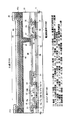
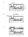
ここで本発明の薄膜形成装置を図1に示し、さらにこの薄膜形成装置を用いた自発光装
置の作製方法について説明する。
Here, the thin film forming apparatus of the present invention is shown in FIG. 1, and a method for manufacturing a self-luminous device using the thin film forming apparatus will be described.
図1(A)は、本発明を実施してπ共役系ポリマーからなる有機EL材料を成膜する様
子を模式的に示す図である。図1(A)において、110は基板であり、基板110上に
は画素部111、ソース側駆動回路112、ゲート側駆動回路113がTFTにより形成
されている。ソース側駆動回路112に接続された複数のソース配線とゲート側駆動回路
113に接続された複数のゲート配線とで囲まれた領域が画素であり、画素内にはTFT
と該TFTに電気的に接続されたEL素子が形成される。画素部111はこのような画素
がマトリクス状の配列されて形成されている。
FIG. 1A is a diagram schematically illustrating a state in which an organic EL material made of a π-conjugated polymer is formed by carrying out the present invention. In FIG. 1A,
And an EL element electrically connected to the TFT. The
なお、本実施例は赤色、緑色、青色のEL層をストライプ状に同時に成膜する方法を示
す。ストライプ状とは、縦横比が2以上の細長い長方形状、長径と短径の比が2以上の細
長い楕円形状を含む。
Note that this example shows a method of simultaneously forming red, green, and blue EL layers in stripes. The stripe shape includes an elongated rectangular shape having an aspect ratio of 2 or more, and an elongated elliptical shape having a ratio of a major axis to a minor axis of 2 or more.
ここで114aは赤色に発光する有機EL材料と溶媒との混合物(以下、赤色EL層用
塗布液という)、114bは緑色に発光する有機EL材料と溶媒との混合物(以下、緑色
EL層用塗布液という)、114cは青色に発光する有機EL材料と溶媒との混合物(以
下、青色EL層用塗布液という)である。なお、これらの有機EL材料はポリマー重合し
たものを直接溶媒に溶かして塗布する方法と、モノマーを溶媒に溶かしたものを成膜した
後に加熱重合させてポリマーとする方法とがあるが、本発明はどちらでも構わない。ここ
ではポリマーとなった有機EL材料を溶媒に溶かして塗布した例を示す。
Here, 114a is a mixture of an organic EL material that emits red light and a solvent (hereinafter referred to as a red EL layer coating liquid), and 114b is a mixture of an organic EL material that emits green light and a solvent (hereinafter referred to as a green EL layer coating). 114c is a mixture of an organic EL material that emits blue light and a solvent (hereinafter referred to as a blue EL layer coating solution). These organic EL materials include a method in which a polymer-polymerized material is directly dissolved in a solvent and a method in which the organic EL material is applied in a solvent, and a method in which a polymer in which a monomer is dissolved in a solvent is formed into a polymer by heat polymerization. Can be either. Here, an example in which an organic EL material that has become a polymer is dissolved in a solvent and applied.
本発明の場合、薄膜形成装置からは赤色EL層用塗布液114a、緑色EL層用塗布液
114b、青色EL層用塗布液114cが別々に吐出され、矢印の方向に向かって塗布され
る。即ち、赤色に発光すべき画素列、緑色に発光すべき画素列及び青色に発光すべき画素
列に、同時にストライプ状のEL層(厳密にはEL層の前駆体)が形成される。
In the case of the present invention, the red EL
なお、ここでいう画素列とはバンク121に仕切られた画素の列を指し、バンク121
はソース配線の上方に形成されている。即ち、ソース配線に沿って複数の画素が直列に並
んだ列を画素列と呼んでいる。但し、ここではバンク121がソース配線の上方に形成さ
れた場合を説明したが、ゲート配線の上方に設けられていても良い。この場合は、ゲート
配線に沿って複数の画素が直列に並んだ列を画素列と呼ぶ。
Note that the pixel column here refers to a column of pixels partitioned by the
Is formed above the source wiring. That is, a column in which a plurality of pixels are arranged in series along the source wiring is called a pixel column. However, although the case where the
従って、画素部111は、複数のソース配線もしくは複数のゲート配線の上方に設けら
れたストライプ状のバンクにより分割された複数の画素列の集合体として見ることができ
る。そのようにして見た場合、画素部111は、赤色に発光するストライプ状のEL層が
形成された画素列、緑色に発光するストライプ状のEL層が形成された画素列及び青色に
発光するストライプ状のEL層が形成された画素列からなるとも言える。
Therefore, the
また、上記ストライプ状のバンクは、複数のソース配線もしくは複数のゲート配線の上
方に設けられているため、実質的に画素部111は、複数のソース配線もしくは複数のゲ
ート配線により分割された複数の画素列の集合体と見ることもできる。
In addition, since the stripe-shaped bank is provided above the plurality of source wirings or the plurality of gate wirings, the
次に、図1(A)に示した塗布工程を行った際の薄膜形成装置のヘッド部(吐出部と言
っても良い)の様子を図1(B)に示す。
Next, FIG. 1B shows a state of the head portion (also referred to as a discharge portion) of the thin film forming apparatus when the coating process shown in FIG.
115は薄膜形成装置のヘッド部であり、赤色用ノズル116a、緑色用ノズル116b
、青色用ノズル116cが取り付けられている。また各々のノズルの内部には赤色EL層
用塗布液114a、緑色EL層用塗布液114b、青色EL層用塗布液114cが蓄えられ
ている。
Reference numeral 115 denotes a head portion of the thin film forming apparatus, and the
A blue nozzle 116c is attached. Also, a red EL
これらの塗布液は、加圧されることにより、画素部111上に吐出される。なお、塗布
液は、ノズル116a、116b、116cと配管117をしきる板(図示せず)に配管
117に充填された不活性ガスを加圧することで吐出される。
このようなヘッド部115が紙面に垂直な方向に沿って手前方向に走査されることで図1
(A)に示したような塗布工程が行われる。
These coating liquids are discharged onto the
Such a head unit 115 is scanned in the front direction along a direction perpendicular to the paper surface, so that FIG.
The coating process as shown in (A) is performed.
なお、ここでは、赤色用ノズル116a、緑色用ノズル116b、青色用ノズル116c
にそれぞれ赤色EL層用塗布液114a、緑色EL層用塗布液114b、青色EL層用塗布
液114cが備えられているが、塗布液は、これらの色に限られることはなく、また、塗
布液を備えているノズルは、一つであっても複数であっても良い。
Here, the
Are provided with a red EL
さらに、ヘッド部115には、塗布液を吐出しやすくするために超音波による振動をあ
たえるための超音波振動子122が取り付けられている。これは、外部の超音波電源に接
続されている。
なお、超音波振動子を取り付ける位置は、図1(B)に示される位置に限られることは
なく、別の位置に付けても良いし、各ノズルに付けても良い。
Furthermore, an
The position where the ultrasonic transducer is attached is not limited to the position shown in FIG. 1B, and may be attached to another position or to each nozzle.
さらに、各ノズル114a、114b、114cには、それぞれヒーター123a、1
23b、123cが設けられている。このヒーターとは、塗布液をうまく吐出するための
塗布液温度調節用に設けられているものであり、ヒーターとなる部分に抵抗材料を存在さ
せると、抵抗材料によりヒーターにかかる電圧が制御できる。電圧が制御されることによ
りヒーター部にかかる温度調節ができるので、ここで用いる抵抗材料は、各塗布液が適温
になるような抵抗を与える材料を選ぶとよい。なお、抵抗材料は、ノズルに接触するよう
に存在させても良いし、ノズルが半導体材料で形成される場合には、ノズル自体に抵抗材
料をドーピングしても良い。また、抵抗材料としては、銅、鉄、アルミニウム、タングス
テン、タンタル、ニッケル、リン、ボロン、ヒ素やアンチモンといった金属を用いる。こ
れにより、吐出液の温度調節が可能となる。
Furthermore, each of the
23b and 123c are provided. The heater is provided for adjusting the temperature of the coating solution for discharging the coating solution well. When a resistance material is present in a portion serving as the heater, the voltage applied to the heater can be controlled by the resistance material. Since the temperature applied to the heater section can be adjusted by controlling the voltage, the resistance material used here may be a material that provides resistance so that each coating solution has an appropriate temperature. The resistance material may be present in contact with the nozzle, or when the nozzle is formed of a semiconductor material, the resistance material may be doped in the nozzle itself. As the resistance material, metals such as copper, iron, aluminum, tungsten, tantalum, nickel, phosphorus, boron, arsenic, and antimony are used. Thereby, the temperature of the discharge liquid can be adjusted.
さらにヒーターとしては、各ノズルのヒーター部分に測温部を設けて各塗布液の温度を
検知し、検知した温度情報をフィードバックさせて新たな電気信号に変換する回路を設け
、この回路に各ヒーターの温度を制御させるような機能を有するものも含める。
Furthermore, as the heater, a temperature measuring unit is provided in the heater portion of each nozzle to detect the temperature of each coating liquid, and a circuit that feeds back the detected temperature information and converts it into a new electric signal is provided in this circuit. Also included are those having a function of controlling the temperature.
また、本明細書中ではヘッド部が走査されるという記載にしているが、基板をX−Yス
テージにより縦方向または横方向に移動させることも可能である。
Further, in this specification, it is described that the head portion is scanned, but the substrate can be moved in the vertical direction or the horizontal direction by the XY stage.
ここで118に示される吐出部付近の拡大図を図1(C)に示す。基板110上に設け
られた画素部111は、複数のTFT119a〜119cと画素電極120a〜120cから
なる複数の画素の集合体である。図1(B)のノズル116a〜116cに圧力がかかると
、その圧力により塗布液114a〜114cが吐出される。
Here, FIG. 1C shows an enlarged view of the vicinity of the discharge portion shown at 118. The
なお、画素間には樹脂材料で形成されたバンク121が設けられており、隣接する画素
間で塗布液が混合されてしまうことを防いでいる。この構造ではバンク121の幅(フォ
トリソグラフィの解像度で決まる)を狭くすることで画素部の集積度が向上し、高精細な
画像を得ることができる。また、ここで用いる塗布液としては、その粘性が1×10⁻³〜
3×10⁻²Pa・sであることが好ましい。
Note that a
It is preferably 3 × 10 −2 Pa · s.
また、バンク121を形成しうる樹脂材料としてはアクリル、ポリイミド、ポリアミド
、ポリイミドアミドを用いることができる。この樹脂材料に予めカーボンや黒色顔料等を
設けて樹脂材料を黒色化しておくと、バンク121を画素間の遮光膜として用いることも
可能となる。
As the resin material that can form the
また、ノズル116a、116bまたは116cのいずれかに光反射を用いたセンサーを
取り付ければ、塗布面とノズルとの距離を常に一定に保つように調節することも可能であ
る。なお、センサーを取り付ける位置は、ノズルの先端が好ましいが、この限りではない
。さらに、画素ピッチ(画素間の距離)に応じてノズル116a〜116cの間隔を調節す
る機構を備えることで、どのような画素ピッチの自発光装置にも対応することが可能であ
る。
Further, if a sensor using light reflection is attached to any of the
こうしてノズル116a〜116cから吐出された塗布液114a〜114cは各々画素電
極120a〜120cを覆うようにして塗布される。塗布液114a〜114cを塗布したら
真空中で加熱処理(ベーク処理または焼成処理)することにより塗布液114a〜114c
に含まれる有機溶媒を揮発させ、有機EL材料からなるEL層を形成する。このため、有
機溶媒は有機EL材料のガラス転移温度(Tg)よりも低い温度で揮発するものを用いる
。また、有機EL材料の粘度により最終的に形成されるEL層の膜厚が決まる。この場合
、粘度は1×10⁻³〜5×10⁻²Pa・s(好ましくは1×10⁻³〜2×10⁻²Pa・s
)とするのが好ましい。
Thus, the
The organic solvent contained in is volatilized to form an EL layer made of an organic EL material. For this reason, an organic solvent is used that volatilizes at a temperature lower than the glass transition temperature (Tg) of the organic EL material. Moreover, the film thickness of the EL layer finally formed is determined by the viscosity of the organic EL material. In this case, the viscosity is 1 × 10 −3 to 5 × 10 −2 Pa · s (preferably 1 × 10 −3 to 2 × 10 −2 Pa · s.
) Is preferred.
さらに、有機EL材料中に不純物が多いと、EL層の劣化原因となり、発光効率が低下
してしまうので有機EL材料中にはできるだけ不純物を低減することが望ましい。
Furthermore, if there are many impurities in the organic EL material, it causes deterioration of the EL layer and the light emission efficiency is lowered. Therefore, it is desirable to reduce impurities in the organic EL material as much as possible.
なお、不純物を低減するには、溶媒及び有機EL材料を徹底的に精製し、溶媒と有機E
L材料を混合する時の環境を可能な限り清浄化することが重要である。
溶媒の精製または有機EL材料の精製は、蒸留法、昇華法、濾過法、再結晶法、再沈殿法
、クロマトグラフィ法または透析法等の技術を繰り返し行うことが好ましい。最終的には
金属元素やアルカリ金属元素等の不純物を0.1ppm以下(好ましくは0.01ppm
以下)にまで低減することが望ましい。
In order to reduce impurities, the solvent and the organic EL material are thoroughly purified, and the solvent and the organic E
It is important to clean as much as possible the environment when mixing the L material.
The purification of the solvent or the organic EL material is preferably performed repeatedly by a technique such as distillation, sublimation, filtration, recrystallization, reprecipitation, chromatography, or dialysis. Ultimately, impurities such as metal elements and alkali metal elements are 0.1 ppm or less (preferably 0.01 ppm).
It is desirable to reduce to below.
また、図1のような薄膜形成装置により有機EL材料を含む塗布液を塗布する際の雰囲
気にも十分に注意することが好ましい。具体的には、上記有機EL材料の成膜工程を、窒
素などの不活性ガスが充填されたクリーンブースやグローブボックス内で行うことが望ま
しい。
Moreover, it is preferable to pay sufficient attention to the atmosphere when the coating liquid containing the organic EL material is applied by the thin film forming apparatus as shown in FIG. Specifically, it is desirable to perform the organic EL material film forming step in a clean booth or glove box filled with an inert gas such as nitrogen.
以上のような薄膜形成装置を用いることにより、塗布液を均一に効率よく塗布すること
ができ、高いスループットでポリマー系有機EL材料からなるEL層を形成することがで
きる。さらに、一つの画素列では切れ間なくストライプ状に塗布していくことができるた
め、非常にスループットが高い。
By using the thin film forming apparatus as described above, the coating liquid can be uniformly and efficiently applied, and an EL layer made of a polymer-based organic EL material can be formed with high throughput. Furthermore, since it can be applied in a striped pattern without a break in one pixel row, the throughput is very high.
本発明を実施することで、有機EL材料を成膜する際に問題となる塗布液の液切れの悪
さや液詰まりに対する改善を図ることができる。また、本発明においては、様々な方法で
有機EL材料を成膜する方法を示しているので、条件や用途に応じて成膜する事が可能で
あり、ポリマー系有機EL材料を用いた自発光装置の製造歩留まりを向上させることがで
きる。
By practicing the present invention, it is possible to improve the poorness of the coating solution that causes problems when the organic EL material is formed into a film and the improvement of clogging. Further, in the present invention, a method for forming an organic EL material by various methods is shown. Therefore, it is possible to form a film according to conditions and applications, and self-light emission using a polymer-based organic EL material. The production yield of the device can be improved.
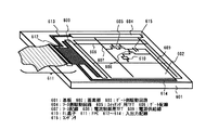
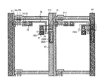
本発明の実施の形態について、図2、図3を用いて説明する。図2に示したのは本発明
の薄膜形成装置を用いて作製した自発光装置の画素部の断面図であり、図3(A)はその
上面図、図3(B)はその回路構成である。実際には画素がマトリクス状に複数配列され
て画素部(画像表示部)が形成される。なお、図3(A)をA−A’で切断した断面図が
図2に相当する。従って図2及び図3で共通の符号を用いているので、適宜両図面を参照
すると良い。また、図3の上面図では二つの画素を図示しているが、どちらも同じ構造で
ある。
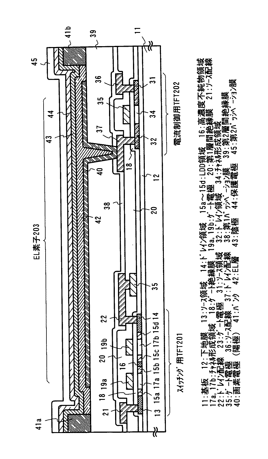
An embodiment of the present invention will be described with reference to FIGS. 2A and 2B are cross-sectional views of a pixel portion of a self-luminous device manufactured using the thin film forming apparatus of the present invention, FIG. 3A is a top view thereof, and FIG. 3B is a circuit configuration thereof. is there. Actually, a plurality of pixels are arranged in a matrix to form a pixel portion (image display portion). Note that a cross-sectional view taken along line AA ′ in FIG. 3A corresponds to FIG. Accordingly, since the same reference numerals are used in FIG. 2 and FIG. 3, both drawings should be referred to as appropriate. Further, in the top view of FIG. 3, two pixels are illustrated, but both have the same structure.
図2において、11は基板、12は下地となる絶縁膜(以下、下地膜という)
である。基板11としてはガラス、ガラスセラミックス、石英、シリコン、セラミックス
、金属若しくはプラスチックからなる基板を用いることができる。
In FIG. 2, 11 is a substrate, 12 is a base insulating film (hereinafter referred to as a base film).
It is. As the
また、下地膜12は特に可動イオンを含む基板や導電性を有する基板を用いる場合に有
効であるが、石英基板には設けなくても構わない。下地膜12としては、珪素(シリコン
)を含む絶縁膜を用いれば良い。なお、本明細書において「珪素を含む絶縁膜」とは、具
体的には酸化珪素膜、窒化珪素膜若しくは窒化酸化珪素膜(SiOxNyで示される)な
ど珪素、酸素若しくは窒素を所定の割合で含む絶縁膜を指す。
The
また、下地膜12に放熱効果を持たせることによりTFTの発熱を発散させることはT
FTの劣化又はEL素子の劣化を防ぐためにも有効である。放熱効果を持たせるには公知
のあらゆる材料を用いることができる。
Further, it is possible to dissipate the heat generated by the TFT by providing the
It is also effective for preventing deterioration of FT or EL element. Any known material can be used to provide a heat dissipation effect.
ここでは画素内に二つのTFTを形成している。201はスイッチング用TFTであり
、nチャネル型TFTで形成され、202は電流制御用TFTであり、pチャネル型TF
Tで形成されている。
Here, two TFTs are formed in the pixel.
T is formed.
ただし、本発明において、スイッチング用TFTをnチャネル型TFT、電流制御用T
FTをpチャネル型TFTに限定する必要はなく、スイッチング用TFTをpチャネル型
TFT、電流制御用TFTをnチャネル型TFTにしたり、両方ともnチャネル型、又は
pチャネル型TFTを用いることも可能である。
However, in the present invention, the switching TFT is an n-channel TFT and the current control T
There is no need to limit the FT to a p-channel TFT, and the switching TFT can be a p-channel TFT and the current control TFT can be an n-channel TFT, or both can be n-channel or p-channel TFTs. It is.
スイッチング用TFT201は、ソース領域13、ドレイン領域14、LDD領域15
a〜15d、高濃度不純物領域16及びチャネル形成領域17a、17bを含む活性層、ゲー
ト絶縁膜18、ゲート電極19a、19b、第1層間絶縁膜20、ソース配線21並びにド
レイン配線22を有して形成される。
The switching
a to 15d, an active layer including the high-
また、図3に示すように、ゲート電極19a、19bは別の材料(ゲート電極19a、1
9bよりも低抵抗な材料)で形成されたゲート配線211によって電気的に接続されたダ
ブルゲート構造となっている。勿論、ダブルゲート構造だけでなく、シングルゲートもし
くはトリプルゲート構造といったいわゆるマルチゲート構造(直列に接続された二つ以上
のチャネル形成領域を有する活性層を含む構造)であっても良い。マルチゲート構造はオ
フ電流値を低減する上で極めて有効であり、本発明では画素のスイッチング素子201を
マルチゲート構造とすることによりオフ電流値の低いスイッチング素子を実現している。
Further, as shown in FIG. 3, the
9b, which is electrically connected by a
また、活性層は結晶構造を含む半導体膜で形成される。即ち、単結晶半導体膜でも良い
し、多結晶半導体膜や微結晶半導体膜でも良い。また、ゲート絶縁膜18は珪素を含む絶
縁膜で形成すれば良い。また、ゲート電極、ソース配線若しくはドレイン配線としてはあ
らゆる導電膜を用いることができる。
The active layer is formed of a semiconductor film including a crystal structure. That is, a single crystal semiconductor film, a polycrystalline semiconductor film, or a microcrystalline semiconductor film may be used. The
さらに、スイッチング用TFT201においては、LDD領域15a〜15dは、ゲート
絶縁膜18を挟んでゲート電極19a、19bと重ならないように設ける。このような構造
はオフ電流値を低減する上で非常に効果的である。
Further, in the switching
なお、チャネル形成領域とLDD領域との間にオフセット領域(チャネル形成領域と同
一組成の半導体層でなり、ゲート電圧が印加されない領域)を設けることはオフ電流値を
下げる上でさらに好ましい。また、二つ以上のゲート電極を有するマルチゲート構造の場
合、チャネル形成領域の間に設けられた高濃度不純物領域がオフ電流値の低減に効果的で
ある。
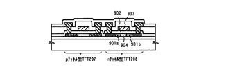
Note that it is more preferable to provide an offset region (a region made of a semiconductor layer having the same composition as the channel formation region to which no gate voltage is applied) between the channel formation region and the LDD region in order to reduce the off-state current value. In the case of a multi-gate structure having two or more gate electrodes, a high-concentration impurity region provided between channel formation regions is effective in reducing the off-current value.
次に、電流制御用TFT202は、ソース領域31、ドレイン領域32及びチャネル形
成領域34を含む活性層、ゲート絶縁膜18、ゲート電極35、第1層間絶縁膜20、ソ
ース配線36並びにドレイン配線37を有して形成される。なお、ゲート電極35はシン
グルゲート構造となっているが、マルチゲート構造であっても良い。
Next, the
図2に示すように、スイッチング用TFTのドレインは電流制御用TFT202のゲー
トに接続されている。具体的には電流制御用TFT202のゲート電極35はスイッチン
グ用TFT201のドレイン領域14とドレイン配線(接続配線とも言える)22を介し
て電気的に接続されている。また、ソース配線36は電源供給線212に接続される。
As shown in FIG. 2, the drain of the switching TFT is connected to the gate of the
電流制御用TFT202はEL素子203に注入される電流量を制御するための素子で
あるが、EL素子の劣化を考慮するとあまり多くの電流を流すことは好ましくない。その
ため、電流制御用TFT202に過剰な電流が流れないように、チャネル長(L)は長め
に設計することが好ましい。望ましくは一画素あたり0.5〜2μA(好ましくは1〜1
.5μA)となるようにする。
The
. 5 μA).
また、スイッチング用TFT201に形成されるLDD領域の長さ(幅)は0.5〜3
.5μm、代表的には2.0〜2.5μmとすれば良い。
The length (width) of the LDD region formed in the switching
. What is necessary is just to set it as 5 micrometers, typically 2.0-2.5 micrometers.
また、図3に示すように電流制御用TFT3503のゲート電極35を含む配線36は
、3504で示される領域で電流制御用TFT3503のドレイン配線37と絶縁膜を挟
んで重なる。このとき3504で示される領域では、保持容量(コンデンサ)が形成され
る。保持容量3504は電源供給線212と電気的に接続された半導体膜3520、ゲー
ト絶縁膜と同一層の絶縁膜(図示せず)及び電源供給線212で形成される容量も保持容
量として用いることが可能である。
この保持容量3504は、電流制御用TFT3503のゲート電極35にかかる電圧を
保持するためのコンデンサとして機能する。
As shown in FIG. 3, the
The holding
また、流しうる電流量を多くするという観点から見れば、電流制御用TFT202の活
性層(特にチャネル形成領域)の膜厚を厚くする(好ましくは50〜100nm、さらに
好ましくは60〜80nm)ことも有効である。逆に、スイッチング用TFT201の場
合はオフ電流値を小さくするという観点から見れば、活性層(特にチャネル形成領域)の
膜厚を薄くする(好ましくは20〜50nm、さらに好ましくは25〜40nm)ことも
有効である。
Further, from the viewpoint of increasing the amount of current that can be passed, the thickness of the active layer (especially the channel formation region) of the
次に、38は第1パッシベーション膜であり、膜厚は10nm〜1μm(好ましくは2
00〜500nm)とすれば良い。材料としては、珪素を含む絶縁膜(特に窒化酸化珪素
膜又は窒化珪素膜が好ましい)を用いることができる。
Next, 38 is a first passivation film having a thickness of 10 nm to 1 μm (preferably 2).
(00 to 500 nm). As a material, an insulating film containing silicon (in particular, a silicon nitride oxide film or a silicon nitride film is preferable) can be used.
第1パッシベーション膜38の上には、各TFTを覆うような形で第2層間絶縁膜(平
坦化膜と言っても良い)39を形成し、TFTによってできる段差の平坦化を行う。第2
層間絶縁膜39としては、有機樹脂膜が好ましく、ポリイミド、ポリアミド、アクリル、
BCB(ベンゾシクロブテン)等を用いると良い。勿論、十分な平坦化が可能であれば、
無機膜を用いても良い。
On the
The
BCB (benzocyclobutene) or the like may be used. Of course, if sufficient flattening is possible,
An inorganic film may be used.
第2層間絶縁膜39によってTFTによる段差を平坦化することは非常に重要である。
後に形成されるEL層は非常に薄いため、段差が存在することによって発光不良を起こす
場合がある。従って、EL層をできるだけ平坦面に形成しうるように画素電極を形成する
前に平坦化しておくことが望ましい。
It is very important to flatten the step due to the TFT by the second
Since an EL layer to be formed later is very thin, a light emission defect may occur due to the presence of a step. Therefore, it is desirable that the EL layer be planarized before forming the pixel electrode so that the EL layer can be formed as flat as possible.
また、40は透明導電膜からなる画素電極(EL素子の陽極に相当する)であり、第2
層間絶縁膜39及び第1パッシベーション膜38にコンタクトホール(開孔)を開けた後
、形成された開孔部において電流制御用TFT202のドレイン配線37に接続されるよ
うに形成される。
After a contact hole (opening) is formed in the
本実施形態では、画素電極として酸化インジウムと酸化スズの化合物からなる導電膜を
用いる。また、これに少量のガリウムを添加しても良い。さらに酸化インジウムと酸化亜
鉛との化合物を用いることもできる。
In this embodiment, a conductive film made of a compound of indium oxide and tin oxide is used as the pixel electrode. Further, a small amount of gallium may be added thereto. Furthermore, a compound of indium oxide and zinc oxide can also be used.
画素電極を形成したら、樹脂材料からなるバンク41aおよび41bを形成する。バン
ク41aおよび41bは1〜2μm厚のアクリル膜またはポリイミド膜をパターニングし
て形成すれば良い。このバンク41aおよび41bは、画素と画素との間にストライプ状
に形成される。本実施例ではソース配線21に沿って形成するがゲート配線35に沿って
形成しても良い。
When the pixel electrode is formed,
次にEL層42が図1で説明したような薄膜形成装置により形成される。なお、ここで
は一画素しか図示していないが、図1で説明したようにR(赤)、G(緑)、B(青)の
各色に対応した発光層が同時に形成される。EL層とする有機EL材料としてはポリマー
系材料を用いる。代表的なポリマー系材料としては、ポリパラフェニレンビニレン(PP
V)系、ポリビニルカルバゾール(PVK)
系、ポリフルオレン系などが挙げられる。
Next, the
V) series, polyvinylcarbazole (PVK)
And polyfluorene type.
なお、PPV系有機EL材料としては様々な型のものがあるが、例えば以下のような分
子式が発表されている。
(「H. Shenk,H.Becker,O.Gelsen,E.Kluge,W.Kreuder,and H.Spreitzer,“Polymers for
Light Emitting Diodes”,Euro Display,Proceedings,1999,p.33-37」)
There are various types of PPV organic EL materials. For example, the following molecular formulas have been announced.
(“H. Shenk, H. Becker, O. Gelsen, E. Kluge, W. Kreuder, and H. Spreitzer,“ Polymers for
Light Emitting Diodes ”, Euro Display, Proceedings, 1999, p. 33-37”)
また、特開平10−92576号公報に記載された分子式のポリフェニルビニルを用い
ることもできる。分子式は以下のようになる。
Further, polyphenylvinyl having a molecular formula described in JP-A-10-92576 can also be used. The molecular formula is:
また、PVK系有機EL材料としては以下のような分子式がある。 The PVK organic EL material has the following molecular formula.
ポリマー系有機EL材料はポリマーの状態で溶媒に溶かして塗布することもできるし、
モノマーの状態で溶媒に溶かして塗布した後に重合することもできる。
モノマーの状態で塗布した場合、まずポリマー前駆体が形成され、真空中で加熱すること
により重合してポリマーになる。
The polymer-based organic EL material can be dissolved in a solvent in the polymer state and applied.
It can also be polymerized after being dissolved in a solvent in the monomer state and coated.
When applied in the monomer state, a polymer precursor is first formed and polymerized by heating in vacuum to a polymer.
具体的なEL層としては、赤色に発光するEL層にはシアノポリフェニレンビニレン、
緑色に発光するEL層にはポリフェニレンビニレン、青色に発光するEL層にはポリフェ
ニレンビニレン若しくはポリアルキルフェニレンを用いれば良い。膜厚は30〜150n
m(好ましくは40〜100nm)とすれば良い。
As a specific EL layer, for the EL layer emitting red light, cyanopolyphenylene vinylene,
Polyphenylene vinylene may be used for the EL layer emitting green light, and polyphenylene vinylene or polyalkylphenylene may be used for the EL layer emitting blue light. Film thickness is 30-150n
m (preferably 40 to 100 nm) may be used.
但し、以上の例は本発明のEL層として用いることのできる有機EL材料の一例であっ
て、これに限定する必要はまったくない。本発明では有機EL材料と溶媒との混合物を図
1に示す方式により塗布して、溶媒を揮発させて除去することによりEL層を形成する。
従って、溶媒を揮発させる際にEL層のガラス転移温度を超えない組み合わせであれば如
何なる有機EL材料を用いても良い。
However, the above example is an example of the organic EL material that can be used as the EL layer of the present invention, and it is not absolutely necessary to limit to this. In the present invention, a mixture of an organic EL material and a solvent is applied by the method shown in FIG. 1, and the EL layer is formed by volatilizing and removing the solvent.
Therefore, any organic EL material may be used as long as the combination does not exceed the glass transition temperature of the EL layer when the solvent is volatilized.
また、代表的な溶媒としてはトルエン、キシレン、クロロベンゼン、ジクロロベンゼン
、アニソール、クロロフォルム、ジクロロメタン、γブチルラクトン、ブチルセルソルブ
、シクロヘキサン、NMP(N−メチル−2−ピロリドン)、シクロヘキサノン、ジオキ
サンまたは、THF(テトラヒドロフラン)が挙げられる。
Typical solvents include toluene, xylene, chlorobenzene, dichlorobenzene, anisole, chloroform, dichloromethane, γ-butyllactone, butyl cellosolve, cyclohexane, NMP (N-methyl-2-pyrrolidone), cyclohexanone, dioxane, or THF. (Tetrahydrofuran).
さらに、EL層42を形成する際、EL層は水分や酸素の存在によって容易に劣化して
しまうため、処理雰囲気は水分や酸素の少ない雰囲気とし、窒素やアルゴンといった不活
性ガス中で行うことが望ましい。さらに処理雰囲気としては、塗布液の蒸発速度を制御で
きることから塗布液作製に用いた溶媒雰囲気にするのも良い。なお、これらを実施するた
めには、図1の薄膜形成装置を、不活性ガスを充填したクリーンブースに設置し、その雰
囲気中で発光層の成膜工程を行うことが望ましい。
Further, when the
以上のようにしてEL層42を形成したら、次に遮光性導電膜からなる陰極43、保護
電極44及び第2パッシベーション膜45が形成される。本実施形態では陰極43として
、MgAgからなる導電膜を用い、保護電極44としてアルミニウムからなる導電膜を用
いる。また、第2パッシベーション膜45としては、10nm〜1μm(好ましくは20
0〜500nm)の厚さの窒化珪素膜を用いる。
After the
A silicon nitride film having a thickness of 0 to 500 nm) is used.
なお、上述のようにEL層は熱に弱いので、陰極43及び第2パッシベーション膜45
はなるべく低温(好ましくは室温から120℃までの温度範囲)で成膜するのが望ましい
。従って、プラズマCVD法、真空蒸着法又は溶液塗布法(スピンコート法)が望ましい
成膜方法と言える。
Since the EL layer is vulnerable to heat as described above, the
It is desirable to form the film at as low a temperature as possible (preferably in a temperature range from room temperature to 120 ° C.). Therefore, it can be said that a plasma CVD method, a vacuum deposition method, or a solution coating method (spin coating method) is a desirable film forming method.
ここまで完成したものをアクティブマトリクス基板とよび、アクティブマトリクス基板
に対向して、対向基板(図示せず)が設けられる。本実施形態では対向基板としてガラス
基板を用いる。なお、対向基板としては、プラスチックやセラミックスからなる基板を用
いても良い。
The completed substrate is called an active matrix substrate, and a counter substrate (not shown) is provided so as to face the active matrix substrate. In this embodiment, a glass substrate is used as the counter substrate. As the counter substrate, a substrate made of plastic or ceramics may be used.
また、アクティブマトリクス基板と対向基板はシール剤(図示せず)によって接着され
、密閉空間(図示せず)が形成される。本実施形態では、密閉空間をアルゴンガスで充填
している。勿論、この密閉空間内に酸化バリウムといった乾燥剤を配置したり酸化防止剤
を配置することも可能である。
Further, the active matrix substrate and the counter substrate are bonded with a sealant (not shown) to form a sealed space (not shown). In this embodiment, the sealed space is filled with argon gas. Of course, it is possible to arrange a desiccant such as barium oxide or an antioxidant in the sealed space.
本発明の実施例における画素部とその周辺に設けられる駆動回路部のTFTを同時に作
製する方法について図4〜図6を用いて説明する。但し、説明を簡単にするために、駆動
回路に関しては基本回路であるCMOS回路を図示することとする。
A method for simultaneously manufacturing TFTs of a pixel portion and a driver circuit portion provided in the periphery thereof in an embodiment of the present invention will be described with reference to FIGS. However, in order to simplify the description, a CMOS circuit, which is a basic circuit, is illustrated with respect to the drive circuit.
まず、図4(A)に示すように、ガラス基板300上に下地膜301を300nmの厚
さに形成する。本実施例では下地膜301として100nm厚の窒化酸化珪素膜と200
nmの窒化酸化珪素膜とを積層して用いる。この時、ガラス基板300に接する方の窒素
濃度を10〜25wt%としておくと良い。もちろん下地膜を設けずに石英基板上に直接
素子を形成しても良い。
First, as shown in FIG. 4A, a
A silicon nitride oxide film having a thickness of nm is stacked and used. At this time, the nitrogen concentration in contact with the
次に下地膜301の上に50nmの厚さの非晶質珪素膜(図示せず))を公知の成膜法
で形成する。なお、非晶質珪素膜に限定する必要はなく、非晶質構造を含む半導体膜(微
結晶半導体膜を含む)であれば良い。さらに非晶質シリコンゲルマニウム膜などの非晶質
構造を含む化合物半導体膜でも良い。また、膜厚は20〜100nmの厚さであれば良い
。
Next, an amorphous silicon film (not shown) having a thickness of 50 nm is formed on the
そして、公知の技術により非晶質珪素膜を結晶化し、結晶質珪素膜(多結晶シリコン膜
若しくはポリシリコン膜ともいう)302を形成する。公知の結晶化方法としては、電熱
炉を使用した熱結晶化方法、レーザー光を用いたレーザーアニール結晶化法、赤外光を用
いたランプアニール結晶化法がある。本実施例では、XeClガスを用いたエキシマレー
ザー光を用いて結晶化する。
Then, the amorphous silicon film is crystallized by a known technique to form a crystalline silicon film (also referred to as a polycrystalline silicon film or a polysilicon film) 302. Known crystallization methods include a thermal crystallization method using an electric furnace, a laser annealing crystallization method using laser light, and a lamp annealing crystallization method using infrared light. In this embodiment, crystallization is performed using excimer laser light using XeCl gas.
なお、本実施例では線状に加工したパルス発振型のエキシマレーザー光を用いるが、矩
形であっても良いし、連続発振型のアルゴンレーザー光や連続発振型のエキシマレーザー
光を用いることもできる。
In this embodiment, a pulse oscillation type excimer laser beam processed into a linear shape is used. However, a rectangular shape, a continuous oscillation type argon laser beam, or a continuous oscillation type excimer laser beam may be used. .
本実施例では結晶質珪素膜をTFTの活性層として用いるが、非晶質珪素膜を用いるこ
とも可能である。また、オフ電流を低減する必要のあるスイッチング用TFTの活性層を
非晶質珪素膜で形成し、電流制御用TFTの活性層を結晶質珪素膜で形成することも可能
である。非晶質珪素膜はキャリア移動度が低いため電流を流しにくくオフ電流が流れにく
い。即ち、電流を流しにくい非晶質珪素膜と電流を流しやすい結晶質珪素膜の両者の利点
を生かすことができる。
In this embodiment, a crystalline silicon film is used as an active layer of a TFT, but an amorphous silicon film can also be used. It is also possible to form the active layer of the switching TFT that needs to reduce the off-current with an amorphous silicon film and form the active layer of the current control TFT with a crystalline silicon film. Since the amorphous silicon film has low carrier mobility, it is difficult for an electric current to flow and an off current is difficult to flow. That is, the advantages of both an amorphous silicon film that hardly allows current to flow and a crystalline silicon film that easily allows current to flow can be utilized.
次に、図4(B)に示すように、結晶質珪素膜302上に酸化珪素膜からなる保護膜3
03を130nmの厚さに形成する。この厚さは100〜200nm(好ましくは130
〜170nm)の範囲で選べば良い。また、珪素を含む絶縁膜であれば他の膜でも良い。
この保護膜303は不純物を添加する際に結晶質珪素膜が直接プラズマに曝されないよう
にするためと、微妙な濃度制御を可能にするために設ける。
Next, as shown in FIG. 4B, a protective film 3 made of a silicon oxide film is formed on the
03 is formed to a thickness of 130 nm. This thickness is 100-200 nm (preferably 130
It may be selected in the range of ˜170 nm. Any other film may be used as long as it is an insulating film containing silicon.
This
そして、その上にレジストマスク304a、304bを形成し、保護膜303を介してn
型を付与する不純物元素(以下、n型不純物元素という)を添加する。
なお、n型不純物元素としては、代表的には15族に属する元素、典型的にはリン又は砒
素を用いることができる。なお、本実施例ではホスフィン(PH3)を質量分離しないで
プラズマ励起したプラズマ(イオン)ドーピング法を用い、リンを1×10¹⁸atoms/cm3
の濃度で添加する。勿論、質量分離を行うイオンインプランテーション法を用いても良い
。
Then, resist
An impurity element imparting a type (hereinafter referred to as an n-type impurity element) is added.
Note that as the n-type impurity element, an element typically belonging to Group 15, typically phosphorus or arsenic can be used. In this embodiment, a plasma (ion) doping method in which phosphine (PH 3 ) is plasma-excited without mass separation is used, and phosphorus is 1 × 10 18 atoms / cm 3.
Add at a concentration of Of course, an ion implantation method for performing mass separation may be used.
この工程により形成されるn型不純物領域305には、n型不純物元素が2×10¹⁶〜
5×10¹⁹atoms/cm3(代表的には5×1017〜5×1018atoms/cm3)
の濃度で含まれるようにドーズ量を調節する。
In the n-
5 × 10 19 atoms / cm 3 (typically 5 × 10 17 to 5 × 10 18 atoms / cm 3 )
The dose is adjusted so that it is contained at a concentration of.
次に、図4(C)に示すように、保護膜303およびレジスト304a、304bを除
去し、添加した15族に属する元素の活性化を行う。活性化手段は公知の技術を用いれば
良いが、本実施例ではエキシマレーザー光の照射により活性化する。勿論、パルス発振型
でも連続発振型でも良いし、エキシマレーザー光に限定する必要はない。但し、添加され
た不純物元素の活性化が目的であるので、結晶質珪素膜が溶融しない程度のエネルギーで
照射することが好ましい。なお、保護膜303をつけたままレーザー光を照射しても良い
。
Next, as shown in FIG. 4C, the
なお、このレーザー光による不純物元素の活性化に際して、熱処理による活性化を併用
しても構わない。熱処理による活性化を行う場合は、基板の耐熱性を考慮して450〜5
50℃程度の熱処理を行えば良い。
Note that activation by heat treatment may be used in combination with the activation of the impurity element by the laser beam. When activation by heat treatment is performed, 450 to 5 is considered in consideration of the heat resistance of the substrate.
A heat treatment at about 50 ° C. may be performed.
この工程によりn型不純物領域305の端部、即ち、n型不純物領域305、の周囲に
存在するn型不純物元素を添加していない領域との境界部(接合部)が明確になる。この
ことは、後にTFTが完成した時点において、LDD領域とチャネル形成領域とが非常に
良好な接合部を形成しうることを意味する。
By this step, an end portion of the n-
次に、図4(D)に示すように、結晶質珪素膜の不要な部分を除去して、島状の半導体
膜(以下、活性層という)306〜309を形成する。
Next, as shown in FIG. 4D, unnecessary portions of the crystalline silicon film are removed, and island-shaped semiconductor films (hereinafter referred to as active layers) 306 to 309 are formed.
次に、図4(E)に示すように、活性層306〜309を覆ってゲート絶縁膜310を
形成する。ゲート絶縁膜310としては、10〜200nm、好ましくは50〜150n
mの厚さの珪素を含む絶縁膜を用いれば良い。これは単層構造でも積層構造でも良い。本
実施例では110nm厚の窒化酸化珪素膜を用いる。
Next, as shown in FIG. 4E, a
An insulating film containing silicon having a thickness of m may be used. This may be a single layer structure or a laminated structure. In this embodiment, a silicon nitride oxide film having a thickness of 110 nm is used.
次に、200〜400nm厚の導電膜を形成し、パターニングしてゲート電極311〜
315を形成する。このゲート電極311〜315の端部をテーパー状にすることもでき
る。なお、本実施例ではゲート電極と、ゲート電極に電気的に接続された引き回しのため
の配線(以下、ゲート配線という)とを別の材料で形成する。具体的にはゲート電極より
も低抵抗な材料をゲート配線として用いる。
これは、ゲート電極としては微細加工が可能な材料を用い、ゲート配線には微細加工はで
きなくとも配線抵抗が小さい材料を用いるためである。勿論、ゲート電極とゲート配線と
を同一材料で形成しても構わない。
Next, a conductive film having a thickness of 200 to 400 nm is formed and patterned to form
315 is formed. The ends of the
This is because a material that can be finely processed is used for the gate electrode, and a material that has a low wiring resistance is used for the gate wiring even though it cannot be finely processed. Of course, the gate electrode and the gate wiring may be formed of the same material.
また、ゲート電極は単層の導電膜で形成しても良いが、必要に応じて二層、三層といっ
た積層膜とすることが好ましい。ゲート電極の材料としては公知のあらゆる導電膜を用い
ることができる。ただし、上述のように微細加工が可能、具体的には2μm以下の線幅に
パターニング可能な材料が好ましい。
The gate electrode may be formed of a single-layer conductive film, but it is preferable to form a stacked film of two layers or three layers as necessary. Any known conductive film can be used as the material of the gate electrode. However, a material that can be finely processed as described above, specifically, that can be patterned to a line width of 2 μm or less is preferable.
代表的には、タンタル(Ta)、チタン(Ti)、モリブデン(Mo)、タングステン
(W)、クロム(Cr)、シリコン(Si)から選ばれた元素からなる膜、または前記元
素の窒化物膜(代表的には窒化タンタル膜、窒化タングステン膜、窒化チタン膜)、また
は前記元素を組み合わせた合金膜(代表的にはMo−W合金、Mo−Ta合金)、または
前記元素のシリサイド膜(代表的にはタングステンシリサイド膜、チタンシリサイド膜)
を用いることができる。勿論、単層で用いても積層して用いても良い。
Typically, a film made of an element selected from tantalum (Ta), titanium (Ti), molybdenum (Mo), tungsten (W), chromium (Cr), and silicon (Si), or a nitride film of the element (Typically a tantalum nitride film, a tungsten nitride film, a titanium nitride film), an alloy film (typically, a Mo—W alloy, a Mo—Ta alloy), or a silicide film of the above elements (typical) (Tungsten silicide film, titanium silicide film)
Can be used. Of course, it may be used as a single layer or may be laminated.
本実施例では、50nm厚の窒化タンタル(TaN)膜と、350nm厚のタンタル(
Ta)膜とからなる積層膜を用いる。これはスパッタ法で形成すれば良い。また、スパッ
タガスとしてXe、Ne等の不活性ガスを添加すると応力による膜はがれを防止すること
ができる。
In this embodiment, a tantalum nitride (TaN) film having a thickness of 50 nm and a tantalum (350 nm thickness) (
A laminated film made of Ta) film is used. This may be formed by sputtering. Further, when an inert gas such as Xe or Ne is added as a sputtering gas, peeling of the film due to stress can be prevented.
またこの時、ゲート電極312はn型不純物領域305の一部とゲート絶縁膜310を
挟んで重なるように形成する。この重なった部分が後にゲート電極と重なったLDD領域
となる。なお、ゲート電極313,314は、断面では、二つに見えるが実際には電気的
に接続されている。
At this time, the
次に、図5(A)に示すように、ゲート電極311〜315をマスクとして自己整合的
にn型不純物元素(本実施例ではリン)を添加する。こうして形成される不純物領域31
6〜323にはn型不純物領域305の1/2〜1/10(代表的には1/3〜1/4)
の濃度でリンが添加されるように調節する。具体的には、1×10¹⁶〜5×10¹⁸atoms/
cm3(典型的には3×10¹⁷〜3×10¹⁸atoms/cm3)の濃度が好ましい。
Next, as shown in FIG. 5A, an n-type impurity element (phosphorus in this embodiment) is added in a self-aligning manner using the
6 to 323 are 1/2 to 1/10 of the n-type impurity region 305 (typically 1/3 to 1/4).
Adjust so that phosphorus is added at a concentration of Specifically, 1 × 10 16 to 5 × 10 18 atoms /
A concentration of cm 3 (typically 3 × 10 17 to 3 × 10 18 atoms / cm 3 ) is preferable.
次に、図5(B)に示すように、ゲート電極等を覆う形でレジストマスク324a〜3
24dを形成し、n型不純物元素(本実施例ではリン)を添加して高濃度にリンを含む不
純物領域325〜329を形成する。ここでもホスフィン(PH3)を用いたイオンドー
プ法で行い、この領域のリンの濃度は1×10²⁰〜1×10²¹atoms/cm3(代表的には2
×1020〜5×10²¹atoms/cm3)となるように調節する。
Next, as shown in FIG. 5B, resist
24d is formed, and an n-type impurity element (phosphorus in this embodiment) is added to form
× 10 20 to 5 × 10 21 atoms / cm 3 ).
この工程によってnチャネル型TFTのソース領域若しくはドレイン領域が形成される
が、スイッチング用TFTでは、図5(A)の工程で形成したn型不純物領域319〜3
21の一部を残す。この残された領域が、図2におけるスイッチング用TFT201のL
DD領域15a〜15dに対応する。
In this step, the source region or drain region of the n-channel TFT is formed. In the switching TFT, the n-
Leave a part of 21. This remaining region is the L of the switching
This corresponds to the
次に、図5(C)に示すように、レジストマスク324a〜324dを除去し、新たに
レジストマスク332を形成する。そして、p型不純物元素(本実施例ではボロン)を添
加し、高濃度にボロンを含む不純物領域333〜336を形成する。ここではジボラン(
B2H6)を用いたイオンドープ法により3×10²⁰〜3×10²¹atoms/cm3(代表的には
5×10²⁰〜1×10²¹atoms/cm3ノ)濃度となるようにボロンを添加する。
Next, as shown in FIG. 5C, the resist
The concentration is 3 × 10 20 to 3 × 10 21 atoms / cm 3 (typically 5 × 10 20 to 1 × 10 21 atoms / cm 3 ) by ion doping using B 2 H 6. Add boron.
なお、不純物領域333〜336には既に1×10²⁰〜1×10²¹atoms/cm3の濃度で
リンが添加されているが、ここで添加されるボロンはその少なくとも3倍以上の濃度で添
加される。そのため、予め形成されていたn型の不純物領域は完全にp型に反転し、p型
の不純物領域として機能する。
Note that phosphorus is already added to the
次に、レジストマスク332を除去した後、それぞれの濃度で添加されたn型またはp
型不純物元素を活性化する。活性化手段としては、ファーネスアニール法、レーザーアニ
ール法、またはランプアニール法で行うことができる。本実施例では電熱炉において窒素
雰囲気中、550℃、4時間の熱処理を行う。
Next, after removing the resist
Activate the type impurity element. As the activation means, furnace annealing, laser annealing, or lamp annealing can be used. In this embodiment, heat treatment is performed in an electric furnace in a nitrogen atmosphere at 550 ° C. for 4 hours.
このとき雰囲気中の酸素を極力排除することが重要である。なぜならば酸素が少しでも
存在していると露呈したゲート電極の表面が酸化され、抵抗の増加を招くと共に後にオー
ミックコンタクトを取りにくくなるからである。従って、上記活性化工程における処理雰
囲気中の酸素濃度は1ppm以下、好ましくは0.1ppm以下とすることが望ましい。
At this time, it is important to eliminate oxygen in the atmosphere as much as possible. This is because the presence of even a small amount of oxygen oxidizes the exposed surface of the gate electrode, which increases resistance and makes it difficult to make ohmic contact later. Therefore, the oxygen concentration in the treatment atmosphere in the activation step is 1 ppm or less, preferably 0.1 ppm or less.
次に、活性化工程が終了したら図5(D)に示すように300nm厚のゲート配線33
7を形成する。ゲート配線337の材料としては、アルミニウム(Al)又は銅(Cu)
を主成分(組成として50〜100%を占める。)とする金属を用いれば良い。配置とし
ては図3のようにゲート配線211とスイッチング用TFTのゲート電極19a、19b(
図4(E)の313、314)が電気的に接続するように形成する。
Next, when the activation process is completed, as shown in FIG.
7 is formed. The material of the
A metal having a main component (occupying 50 to 100% as a composition) may be used. As shown in FIG. 3, the
In FIG. 4E, 313 and 314) are formed so as to be electrically connected.
このような構造とすることでゲート配線の配線抵抗を非常に小さくすることができるた
め、面積の大きい画像表示領域(画素部)を形成することができる。即ち、画面の大きさ
が対角10インチ以上(さらには30インチ以上)の自発光装置を実現する上で、本実施
例の画素構造は極めて有効である。
With such a structure, the wiring resistance of the gate wiring can be extremely reduced, so that an image display region (pixel portion) having a large area can be formed. That is, the pixel structure of this embodiment is extremely effective in realizing a self-luminous device having a screen size of 10 inches or more (or 30 inches or more) diagonally.
次に、図6(A)に示すように、第1層間絶縁膜338を形成する。第1層間絶縁膜3
38としては、珪素を含む絶縁膜を単層で用いるか、2種類以上の珪素を含む絶縁膜を組
み合わせた積層膜を用いれば良い。また、膜厚は400nm〜1.5μmとすれば良い。
本実施例では、200nm厚の窒化酸化珪素膜の上に800nm厚の酸化珪素膜を積層し
た構造とする。
Next, as shown in FIG. 6A, a first
As 38, an insulating film containing silicon may be used as a single layer, or a laminated film in which two or more kinds of insulating films containing silicon are combined may be used. The film thickness may be 400 nm to 1.5 μm.
In this embodiment, a structure is formed in which a silicon oxide film having a thickness of 800 nm is stacked on a silicon nitride oxide film having a thickness of 200 nm.
さらに、3〜100%の水素を含む雰囲気中で、300〜450℃で1〜12時間の熱
処理を行い、水素化処理をする。この工程は熱的に励起された水素により半導体膜の不対
結合手を水素終端する工程である。水素化の他の手段として、プラズマ水素化(プラズマ
化して生成された水素を用いる)を行っても良い。
Further, a hydrogenation treatment is performed by performing a heat treatment at 300 to 450 ° C. for 1 to 12 hours in an atmosphere containing 3 to 100% hydrogen. This step is a step in which the dangling bonds of the semiconductor film are terminated with hydrogen by thermally excited hydrogen. As another means for hydrogenation, plasma hydrogenation (using hydrogen generated by plasmatization) may be performed.
なお、水素化処理は第1層間絶縁膜338を形成する間に入れても良い。即ち、200
nm厚の窒化酸化珪素膜を形成した後で上記のように水素化処理を行い、その後で残り8
00nm厚の酸化珪素膜を形成してもよい。
Note that the hydrogenation treatment may be performed while the first
After forming a silicon nitride oxide film having a thickness of nm, hydrogenation is performed as described above, and then the remaining 8
A 00 nm thick silicon oxide film may be formed.
次に、第1層間絶縁膜338及びゲート絶縁膜310に対してコンタクトホールを形成
し、ソース配線339〜342と、ドレイン配線343〜345を形成する。なお、本実
施例ではこの電極を、Ti膜を100nm、Tiを含むアルミニウム膜を300nm、T
i膜150nmをスパッタ法で連続形成した3層構造の積層膜とする。勿論、他の導電膜
でも良い。
Next, contact holes are formed in the first
A laminated film having a three-layer structure in which an i film of 150 nm is continuously formed by sputtering is used. Of course, other conductive films may be used.
次に、50〜500nm(代表的には200〜300nm)の厚さで第1パッシベーシ
ョン膜346を形成する。本実施例では第1パッシベーション膜346として300nm
厚の窒化酸化珪素膜を用いる。これは窒化珪素膜で代用しても良い。
Next, a
A thick silicon nitride oxide film is used. This may be replaced by a silicon nitride film.
なお、窒化酸化珪素膜の形成に先立ってH2、NH3等水素を含むガスを用いてプラズマ
処理を行うことは有効である。この前処理により励起された水素が第1層間絶縁膜338
に供給され、熱処理を行うことで、第1パッシベーション膜346の膜質が改善される。
それと同時に、第1層間絶縁膜338に添加された水素が下層側に拡散するため、効果的
に活性層を水素化することができる。
Note that it is effective to perform plasma treatment using a gas containing hydrogen such as H 2 or NH 3 prior to formation of the silicon nitride oxide film. The hydrogen excited by this pretreatment becomes the first
The film quality of the
At the same time, hydrogen added to the first
次に、図6(B)に示すように有機樹脂からなる第2層間絶縁膜347を形成する。有
機樹脂としては、ポリイミド、ポリアミド、アクリル、BCB(ベンゾシクロブテン)等
を使用することができる。特に、第2層間絶縁膜347は平坦化の意味合いが強いので、
平坦性に優れたアクリルが好ましい。本実施例ではTFTによって形成される段差を十分
に平坦化しうる膜厚でアクリル膜を形成する。好ましくは1〜5μm(さらに好ましくは
2〜4μm)とすれば良い。
Next, as shown in FIG. 6B, a second
Acrylic having excellent flatness is preferred. In this embodiment, the acrylic film is formed with a film thickness that can sufficiently flatten the step formed by the TFT. The thickness is preferably 1 to 5 μm (more preferably 2 to 4 μm).
次に、第2層間絶縁膜347及び第1パッシベーション膜346に対してコンタクトホ
ールを形成し、ドレイン配線345と電気的に接続される画素電極348を形成する。本
実施例では酸化インジウム・スズ(ITO)膜を110nmの厚さに形成し、パターニン
グを行って画素電極とする。また、酸化インジウムに2〜20%の酸化亜鉛(ZnO)を
混合した透明導電膜を用いても良い。この画素電極がEL素子の陽極となる。
Next, contact holes are formed in the second
次に、図6(C)に示すように、樹脂材料からなるバンク349を形成する。
バンク349は1〜2μm厚のアクリル膜またはポリイミド膜をパターニングして形成す
れば良い。このバンク349は図3に示したように、画素と画素との間にストライプ状に
形成される。本実施例ではソース配線341に沿って形成するがゲート配線337に沿っ
て形成しても良い。
Next, as shown in FIG. 6C, a
The
次に、EL層350を、図1を用いて説明した薄膜形成装置を用いた成膜工程により形
成する。具体的には、EL層350となる有機EL材料をクロロフォルム、ジクロロメタ
ン、キシレン、トルエン、テトラヒドロフラン、N−メチルピロリドンといった溶媒に溶
かして塗布し、その後、熱処理を行うことにより溶媒を揮発させる。こうして有機EL材
料からなる被膜(EL層)が形成される。
Next, the
なお、本実施例では一画素しか図示されていないが、このとき同時に赤色に発光するE
L層、緑色に発光するEL層及び青色に発光するEL層が形成される。
本実施例では、赤色に発光するEL層としてシアノポリフェニレンビニレン、緑色に発
光するEL層としてポリフェニレンビニレン、青色に発光するEL層としてポリアルキル
フェニレンを各々50nmの厚さに形成する。また、溶媒としては1,2−ジクロロメタ
ンを用い、80〜150℃のホットプレートで1〜5分の熱処理を行って揮発させる。
In this embodiment, only one pixel is shown, but at this time, E is emitted in red at the same time.
An L layer, an EL layer emitting green light, and an EL layer emitting blue light are formed.
In this embodiment, cyanopolyphenylene vinylene is formed as an EL layer emitting red light, polyphenylene vinylene is formed as an EL layer emitting green light, and polyalkylphenylene is formed as an EL layer emitting blue light to a thickness of 50 nm. In addition, 1,2-dichloromethane is used as a solvent, and is volatilized by performing heat treatment for 1 to 5 minutes on a hot plate at 80 to 150 ° C.
なお、EL層350としては公知の材料を用いることができる。公知の材料としては、
駆動電圧を考慮すると有機材料を用いるのが好ましい。なお、本実施例ではEL層350
を上記EL層のみの単層構造とするが、必要に応じて電子注入層、電子輸送層、正孔輸送
層、正孔注入層、電子阻止層もしくは正孔素子層を設けても良い。また、本実施例ではE
L素子の陰極351としてMgAg電極を用いた例を示すが、公知の他の材料であっても
良い。
Note that a known material can be used for the
Considering the driving voltage, it is preferable to use an organic material. In this embodiment, the
Is a single-layer structure composed of only the EL layer, but an electron injection layer, an electron transport layer, a hole transport layer, a hole injection layer, an electron blocking layer, or a hole element layer may be provided as necessary. In this embodiment, E
An example in which an MgAg electrode is used as the
EL層350を形成した後、陰極(MgAg電極)351を真空蒸着法を用いて形成す
る。なお、EL層350の膜厚は80〜200nm(典型的には100〜120nm)、
陰極351の厚さは180〜300nm(典型的には200〜250nm)とすれば良い
。
After the
The thickness of the
さらに、陰極351上には、保護電極352を設ける。保護電極352としてはアルミ
ニウムを主成分とする導電膜を用いれば良い。保護電極352は、マスクを用いて真空蒸
着法で形成すれば良い。
Further, a
最後に、窒化珪素膜からなる第2パッシベーション膜353を300nmの厚さに形成
する。実際には保護電極352がEL層を水分等から保護する役割を果たすが、さらに第
2パッシベーション膜353を形成しておくことで、EL素子の信頼性をさらに高めるこ
とができる。
Finally, a
本実施例の場合、図6(C)に示すように、nチャネル型205の活性層は、ソース領
域355、ドレイン領域356、LDD領域357及びチャネル形成領域358を含み、
LDD領域357はゲート絶縁膜310を挟んでゲート電極312と重なっている。
In this embodiment, as shown in FIG. 6C, the active layer of the n-
The
ドレイン領域側のみにLDD領域を形成しているのは、動作速度を落とさないための配
慮である。また、このnチャネル型TFT205はオフ電流値をあまり気にする必要はな
く、それよりも動作速度を重視した方が良い。従って、LDD領域357は完全にゲート
電極に重ねてしまい、極力抵抗成分を少なくすることが望ましい。即ち、いわゆるオフセ
ットはなくした方がよい。
The reason why the LDD region is formed only on the drain region side is to prevent the operation speed from being lowered. In addition, the n-
こうして図6(C)に示すような構造のアクティブマトリクス基板が完成する。なお、
バンク349を形成した後、パッシベーション膜353を形成するまでの工程をマルチチ
ャンバー方式(またはインライン方式)の薄膜形成装置を用いて、大気解放せずに連続的
に処理することは有効である。
Thus, an active matrix substrate having a structure as shown in FIG. 6C is completed. In addition,
It is effective to continuously process the steps from the formation of the
ところで、本実施例のアクティブマトリクス基板は、画素部だけでなく駆動回路部にも
最適な構造のTFTを配置することにより、非常に高い信頼性を示し、動作特性も向上し
うる。
By the way, the active matrix substrate of this embodiment can provide extremely high reliability and improve the operating characteristics by arranging TFTs having an optimal structure not only in the pixel portion but also in the drive circuit portion.
まず、極力動作速度を落とさないようにホットキャリア注入を低減させる構造を有する
TFTを、駆動回路部を形成するCMOS回路のnチャネル型TFT205として用いる
。なお、ここでいう駆動回路としては、シフトレジスタ、バッファ、レベルシフタ、サン
プリング回路(サンプル及びホールド回路)などが含まれる。デジタル駆動を行う場合に
は、D/Aコンバータなどの信号変換回路も含まれうる。
First, a TFT having a structure that reduces hot carrier injection so as not to decrease the operating speed as much as possible is used as an n-
なお、駆動回路の中でもサンプリング回路は他の回路と比べて少し特殊であり、チャネ
ル形成領域を双方向に大電流が流れる。即ち、ソース領域とドレイン領域の役割が入れ替
わるのである。さらに、オフ電流値を極力低く抑える必要があり、そういった意味でスイ
ッチング用TFTと電流制御用TFTの中間程度の機能を有するTFTを配置することが
望ましい。
Note that the sampling circuit in the driver circuit is a little special compared to other circuits, and a large current flows in both directions in the channel formation region. That is, the roles of the source region and the drain region are interchanged. Furthermore, it is necessary to keep the off-current value as low as possible, and in that sense, it is desirable to dispose a TFT having an intermediate function between the switching TFT and the current control TFT.
従って、サンプリング回路を形成するnチャネル型TFTは、図7に示すような構造の
TFTを配置することが望ましい。図7に示すように、LDD領域901a、901bの一
部がゲート絶縁膜902を介してゲート電極903と重なる。
この効果は電流を流した際に生じるホットキャリア注入に対する劣化対策であり、サンプ
リング回路の場合はチャネル形成領域904を挟む形で両側に設ける点が異なる。
Therefore, it is desirable to dispose a TFT having a structure as shown in FIG. 7 as the n-channel TFT forming the sampling circuit. As shown in FIG. 7,
This effect is a countermeasure against deterioration against hot carrier injection that occurs when a current is passed. In the case of a sampling circuit, it is different in that it is provided on both sides with a
なお、実際には図6(C)まで完成したら、さらに外気に曝されないように気密性の高
いガラス、石英、プラスチックといったハウジング材でパッケージング(封入)すること
が好ましい。その際、ハウジング材の内部に内部に酸化バリウムといった吸湿剤や酸化防
止剤を配置するとよい。
Actually, after completion of FIG. 6C, it is preferable to package (enclose) with a housing material such as highly airtight glass, quartz, or plastic so as not to be exposed to the outside air. In that case, it is good to arrange | position a moisture absorbent and antioxidant, such as barium oxide, inside a housing material.
また、パッケージング等の処理により気密性を高めたら、基板上に形成された素子又は
回路から引き回された端子と外部信号端子とを接続するためのコネクター(フレキシブル
プリントサーキット:FPC)を取り付けて製品として完成する。このような出荷できる
状態にまでした状態を本明細書中では自発光装置(またはELモジュール)をという。
In addition, when the airtightness is improved by processing such as packaging, a connector (flexible printed circuit: FPC) for connecting the terminal routed from the element or circuit formed on the substrate and the external signal terminal is attached. Completed as a product. In this specification, such a state that can be shipped is referred to as a self-luminous device (or EL module).
ここで本実施例のアクティブマトリクス型自発光装置の構成を図8の斜視図を用いて説
明する。本実施例のアクティブマトリクス型自発光装置は、ガラス基板601上に形成さ
れた、画素部602と、ゲート側駆動回路603と、ソース側駆動回路604を含む。画
素部のスイッチング用TFT605はnチャネル型TFTであり、ゲート側駆動回路60
3に接続されたゲート配線606、ソース側駆動回路604に接続されたソース配線60
7の交点に配置されている。また、スイッチング用TFT605のドレインは電流制御用
TFT608のゲートに接続されている。
Here, the configuration of the active matrix self-luminous device of this embodiment will be described with reference to the perspective view of FIG. The active matrix self-luminous device of this embodiment includes a
3 and the source wiring 60 connected to the source
7 at the intersection. The drain of the switching
さらに、電流制御用TFT608のソース側は電源供給線609に接続される。本実施
例のような構造では、電源供給線609には接地電位(アース電位)が与えられている。
また、電流制御用TFT608のドレインにはEL素子610が接続されている。また、
このEL素子610の陽極には所定の電圧(3〜12V、好ましくは3〜5V)が加えら
れる。
Further, the source side of the
An
A predetermined voltage (3 to 12 V, preferably 3 to 5 V) is applied to the anode of the
そして、外部入出力端子となるFPC611には駆動回路部まで信号を伝達するための
接続配線612、613、及び電源供給線609に接続された接続配線614が設けられ
ている。
The
また、図8に示した自発光装置の回路構成の一例を図9に示す。本実施例の自発光装置
は、ソース側駆動回路801、ゲート側駆動回路(A)807、ゲート側駆動回路(B)
811、画素部806を有している。なお、本明細書中において、駆動回路部とはソース
側処理回路およびゲート側駆動回路を含めた総称である。
FIG. 9 shows an example of the circuit configuration of the self light emitting device shown in FIG. The self-light emitting device of this embodiment includes a source side driver circuit 801, a gate side driver circuit (A) 807, and a gate side driver circuit (B).
811 and a pixel portion 806. Note that in this specification, the drive circuit portion is a generic term including a source side processing circuit and a gate side drive circuit.
ソース側駆動回路801は、シフトレジスタ802、レベルシフタ803、バッファ8
04、サンプリング回路(サンプル及びホールド回路)805を備えている。また、ゲー
ト側駆動回路(A)807は、シフトレジスタ808、レベルシフタ809、バッファ8
10を備えている。ゲート側駆動回路(B)811も同様な構成である。
The source side drive circuit 801 includes a shift register 802, a level shifter 803, and a buffer 8
04, a sampling circuit (sample and hold circuit) 805 is provided. The gate side driver circuit (A) 807 includes a
10 is provided. The gate side driver circuit (B) 811 has a similar structure.
ここでシフトレジスタ802、808は駆動電圧が5〜16V(代表的には10V)で
あり、回路を形成するCMOS回路に使われるnチャネル型TFTは図6(C)の205
で示される構造が適している。
Here, the driving voltages of the shift registers 802 and 808 are 5 to 16 V (typically 10 V), and an n-channel TFT used in a CMOS circuit forming the circuit is 205 in FIG.
The structure shown by is suitable.
また、レベルシフタ803、809、バッファ804、810はシフトレジスタと同様
に、図6(C)のnチャネル型TFT205を含むCMOS回路が適している。なお、ゲ
ート配線をダブルゲート構造、トリプルゲート構造といったマルチゲート構造とすること
は、各回路の信頼性を向上させる上で有効である。
As the
また、サンプリング回路805はソース領域とドレイン領域が反転する上、オフ電流値
を低減する必要があるので、図7のnチャネル型TFT208を含むCMOS回路が適し
ている。
In addition, since the sampling circuit 805 needs to reduce the off current value in addition to the inversion of the source region and the drain region, a CMOS circuit including the n-channel TFT 208 in FIG. 7 is suitable.
また、画素部806は図2に示した構造の画素を配置する。 In addition, the pixel portion 806 includes pixels having the structure shown in FIG.
なお、上記構成は、図4〜6に示した作製工程に従ってTFTを作製することによって
容易に実現することができる。また、本実施例では画素部と駆動回路部の構成のみ示して
いるが、本実施例の作製工程に従えば、その他にも信号分割回路、D/Aコンバータ回路
、オペアンプ回路、γ補正回路など駆動回路以外の論理回路を同一基板上に形成すること
が可能であり、さらにはメモリ部やマイクロプロセッサ等を形成しうると考えている。
In addition, the said structure can be easily implement | achieved by manufacturing TFT according to the manufacturing process shown to FIGS. Further, in this embodiment, only the configuration of the pixel portion and the drive circuit portion is shown. However, according to the manufacturing process of this embodiment, a signal dividing circuit, a D / A converter circuit, an operational amplifier circuit, a γ correction circuit, etc. It is considered that logic circuits other than the drive circuit can be formed on the same substrate, and further, a memory portion, a microprocessor, and the like can be formed.
さらに、ハウジング材をも含めた本実施例のELモジュールについて図10(A)、(
B)を用いて説明する。なお、必要に応じて図8、図9で用いた符号を引用することにす
る。
Further, the EL module of this embodiment including the housing material is shown in FIGS.
A description will be given using B). Note that the reference numerals used in FIGS. 8 and 9 are cited as necessary.
図10(A)は、図8に示した状態にシーリング構造を設けた状態を示す上面図である
。点線で示された602は画素部、603はゲート側駆動回路、604はソース側駆動回
路である。本発明のシーリング構造は、図8の状態に対して充填材(図示せず)、ハウジ
ング材1101、シール材(図示せず)及びフレーム材1102を設けた構造である。
FIG. 10A is a top view showing a state in which a sealing structure is provided in the state shown in FIG.
ここで、図10(A)をA−A’で切断した断面図を図10(B)に示す。なお、図1
0(A)、(B)では同一の部位に同一の符号を用いている。
Here, FIG. 10B is a cross-sectional view taken along line AA ′ of FIG. In addition, FIG.
In 0 (A) and (B), the same symbols are used for the same parts.
図10(B)に示すように、基板601上には画素部602、ゲート側駆動回路603
が形成されており、画素部602は電流制御用TFT202とそれに電気的に接続された
画素電極348を含む複数の画素により形成される。また、ゲート側駆動回路603はn
チャネル型TFT205とpチャネル型TFT206とを相補的に組み合わせたCMOS
回路を用いて形成される。
As shown in FIG. 10B, a
The
CMOS in which
It is formed using a circuit.
画素電極348はEL素子の陽極として機能する。また、画素電極348の両端にはバ
ンク349が形成され、バンク349の内側にEL層350、陰極351が形成される。
また、その上には保護電極352、第2パッシベーション膜353が形成される。勿論、
発明の実施の形態にも述べたようにEL素子の構造を反対とし、画素電極を陰極としても
構わない。
The
A
As described in the embodiment of the invention, the structure of the EL element may be reversed and the pixel electrode may be a cathode.
本実施例の場合、保護電極352は全画素に共通の配線としても機能し、接続配線61
2を経由してFPC611に電気的に接続されている。さらに、画素部602及びゲート
側駆動回路603に含まれる素子は全て第2パッシベーション膜353で覆われている。
この第2パッシベーション膜353は省略することも可能であるが、各素子を外部と遮断
する上で設けた方が好ましい。
In this embodiment, the
2 to be electrically connected to the
Although the
次に、EL素子を覆うようにして充填材1103を設ける。この充填材1103はハウ
ジング材1101を接着するための接着剤としても機能する。充填材1103としては、
PVC(ポリビニルクロライド)、エポキシ樹脂、シリコン樹脂、PVB(ポリビニルブ
チラル)またはEVA(エチレンビニルアセテート)
を用いることができる。この充填材1103の内部に乾燥剤(図示せず)を設けておくと
、吸湿効果を保ち続けられるので好ましい。このとき、乾燥剤は充填材に添加されたもの
であっても良いし、充填材に封入されたものであっても良い。
また、上述した充填材の代わりに不活性ガス(窒素、アルゴン、ヘリウム等)の他、不活
性液体(パーフルオロアルカンに代表されるのは、液状フッ素化炭素等である)を充填さ
せてもよい。
Next, a
PVC (polyvinyl chloride), epoxy resin, silicone resin, PVB (polyvinyl butyral) or EVA (ethylene vinyl acetate)
Can be used. It is preferable to provide a desiccant (not shown) inside the
In addition to the above-described filler, an inert gas (nitrogen, argon, helium, etc.) or an inert liquid (perfluoroalkane is represented by liquid fluorinated carbon, etc.) may be filled. Good.
また、本実施例ではハウジング材1101としては、ガラス、プラスチック、およびセ
ラミックスからなる材料を用いることができる。なお、充填材1103の内部に予め酸化
バリウム等の吸湿剤を添加しておくことは有効である。
In this embodiment, the
次に、充填材1103を用いてハウジング材1101を接着した後、充填材1103の
側面(露呈面)を覆うようにフレーム材1102を取り付ける。フレーム材1102はシ
ール材(接着剤として機能する)1104によって接着される。このとき、シール材11
04としては、光硬化性樹脂を用いるのが好ましいが、EL層の耐熱性が許せば熱硬化性
樹脂を用いても良い。なお、シール材1104はできるだけ水分や酸素を透過しない材料
であることが望ましい。また、シール材1104の内部に乾燥剤を添加してあっても良い
。
Next, after the
As 04, a photocurable resin is preferably used, but a thermosetting resin may be used if the heat resistance of the EL layer permits. Note that the sealing
以上のような方式を用いてEL素子を充填材1103に封入することにより、EL素子
を外部から完全に遮断することができ、外部から水分や酸素等のEL層の酸化による劣化
を促す物質が侵入することを防ぐことができる。従って、信頼性の高い自発光装置を作製
することができる。なお、本実施例において、赤色、緑色または青色に発光する三種類の
ストライプ状のEL層を同時に縦方向または横方向に形成する例を示したがストライプ状
のEL層を長手方向において複数に分割して形成しても良い。
By encapsulating the EL element in the
また、本実施例では赤色に発光するEL層、緑色に発光するEL層、青色に発光するE
L層の全てを図1の薄膜形成装置を用いて形成する例を示しているが、図1の薄膜形成装
置を用いるEL層は赤色用、緑色用または青色用の少なくとも一つであっても良い。
In this embodiment, the EL layer emitting red light, the EL layer emitting green light, and the E emitting blue light.
Although an example in which all of the L layer is formed using the thin film forming apparatus of FIG. 1 is shown, the EL layer using the thin film forming apparatus of FIG. 1 may be at least one for red, green or blue good.
次に、図2において説明した画素部におけるコンタクト構造に改良を加える際の作製方
法について図11の断面図を用いて説明する。なお、図11における番号は、図2におけ
る番号に対応している。本実施例1の工程に従って、図11(A)に示すようにEL素子
を構成する画素電極(陽極)40が設けられている状態を得る。
Next, a manufacturing method when the contact structure in the pixel portion described in FIG. 2 is improved will be described with reference to the cross-sectional view of FIG. The numbers in FIG. 11 correspond to the numbers in FIG. According to the process of the first embodiment, a state is provided in which the pixel electrode (anode) 40 constituting the EL element is provided as shown in FIG.
次に画素電極上のコンタクト部1900をアクリルで埋め、図11(B)に示すように
コンタクトホール保護部1901を設ける。ここでは、アクリルをスピンコート法により
成膜し、レジストマスクを用いて露光した後、エッチングを行うことにより図11(B)
に示すようなコンタクトホール保護部1901を形成させる。
Next, the contact portion 1900 on the pixel electrode is filled with acrylic, and a contact
A contact
なお、コンタクトホール保護部1901は、断面から見て画素電極よりも盛り上がって
いる部分(図11(B)のDaに示す部分)の厚さが0.1〜1μm、好ましくは0.1
〜0.5μm、さらに好ましくは0.1〜0.3μmとなるのがよい。コンタクトホール
保護部1901が形成されると、図11(C)に示すようにEL層42が形成され、さら
に陰極43が形成される。EL層42及び陰極43の作製方法は、実施例1と同様の方法
を用いればよい。
Note that in the contact
It is good to be -0.5 micrometer, More preferably, it is 0.1-0.3 micrometer. When the contact
また、コンタクトホール保護部1901には、有機樹脂が好ましく、ポリイミド、ポリ
アミド、アクリル、BCB(ベンゾシクロブテン)といった材料を用いると良い。また、
これらの有機樹脂を用いる際には、粘度を10-3Pa・s〜10-1Pa・sとするとよい
。
The contact
When using these organic resins, the viscosity may be 10 −3 Pa · s to 10 −1 Pa · s.
以上のようにして図11(C)に示す様な構造とすることで、コンタクトホールの段差
部分で、EL層42が切断された際に生じる画素電極40と陰極43間での短絡の問題を
解決することができる。また、図11で示した画素部の上面図を図12に示す。なお、図
12で使用される番号は、図11の番号と一致しており、本実施例で示したコンタクトホ
ール保護部1901は上面図で見ると図12の1901で示される位置にあたる。
With the structure as shown in FIG. 11C as described above, there is a problem of short circuit between the
また、本実施例の構成は、実施例1の構成と自由に組み合わせることができる。 Further, the configuration of the present embodiment can be freely combined with the configuration of the first embodiment.
実施例1では、本発明を実施する上でEL層を形成する際に、塗布液が加圧されること
により各ノズルから塗布液が画素部に吐出される加圧タイプの塗布方法を用いた。本実施
例では、塗布方法として各ノズルが一本の管からなる柔軟で微細な接触子からなり、この
接触子が画素部のバンクに接触することにより塗布液が画素部に吐出されるという毛管現
象を利用した万年筆タイプの塗布方法を用いた例を示す。
In Example 1, when the EL layer was formed in carrying out the present invention, a pressure type coating method in which the coating liquid was discharged from each nozzle to the pixel portion when the coating liquid was pressurized was used. . In this embodiment, as a coating method, each nozzle is composed of a flexible and fine contact consisting of a single tube, and the contact is brought into contact with the bank of the pixel portion, whereby the coating liquid is discharged to the pixel portion. An example using a fountain pen type application method utilizing the phenomenon is shown.
図13(A)に示すように、基板110上にはTFTによって画素部111、ソース側
駆動回路112、ゲート側駆動回路113が形成され、画素部111はバンク121によ
ってストライプ状に分割されている。
As shown in FIG. 13A, a
本実施例では、図13の薄膜形成装置を用いてEL層として機能する有機EL材料の成
膜工程を行う。ヘッド部124には、赤色用ノズル125a、緑色用ノズル125b、青色
用ノズル125cが取り付けられている。これらのノズルの先端には、管状の部品がつい
ており、これを本明細書中では、接触子と呼ぶ。なお、赤色用ノズル125a、緑色用ノ
ズル125b、青色用ノズル125cに取り付けられている接触子をそれぞれ接触子129
a、接触子129b、接触子129cとよぶ。
In this embodiment, a film forming process of an organic EL material functioning as an EL layer is performed using the thin film forming apparatus of FIG. A red nozzle 125a, a green nozzle 125b, and a blue nozzle 125c are attached to the head portion 124. At the tips of these nozzles, tubular parts are attached, which are referred to as contacts in this specification. Note that the contacts attached to the red nozzle 125a, the green nozzle 125b, and the blue nozzle 125c are the contact elements 129, respectively.
a,
この接触子は、シリコン、ゲルマニウムといった半導体材料、鉄、銅、アルミニウム、
ステンレスといった金属、ゴム、テフロン(登録商標)、ガラスやプラスチックでできて
いる。そして、接触子の一端がバンクに接触することにより毛管現象でノズル中の塗布液
が注入される。なお、各々のノズルの内部には赤色EL層用塗布液114a、緑色EL層
用塗布液114b、青色EL層用塗布液114cが蓄えられている。取り付けられたノズル
よって同時に赤色用塗布液114a、緑色用塗布液114b及び青色用塗布液114cを塗
り分ける。
This contact is made of semiconductor materials such as silicon and germanium, iron, copper, aluminum,
It is made of metal such as stainless steel, rubber, Teflon (registered trademark), glass or plastic. And the coating liquid in a nozzle is inject | poured by capillary action when the end of a contactor contacts a bank. In each nozzle, a red EL
さらに、ヘッド部124には、超音波振動子122が取り付けられており、また、各ノ
ズル125a、125b、125cには、ヒーター123a、123b、123cがそれ
ぞれ取り付けられている。この超音波振動子及びヒーターは、本明細書中の本実施の形態
で示すように塗布液を塗布しやすくするために設けられている。
Furthermore, an
本実施例における特徴は、塗布する位置を一度決めれば、バンク121に沿って塗布液
が塗布されるため塗布位置がずれにくいという点にある。
The feature of the present embodiment is that once the position to be applied is determined, the application position is difficult to shift because the application liquid is applied along the
また、本実施例においては、ヘッド部124がaで示される方向に移動するのに伴って
塗布液が塗布されるだけでなく、毛管現象によっても塗布液が塗布面に広がるのでより均
一に効率よく塗布液を塗布することができる。この動作を繰り返して画素部に塗布液を塗
布していき、その後、熱処理により溶媒を揮発させて有機EL材料を形成する。
Further, in the present embodiment, the coating liquid is not only applied as the head portion 124 moves in the direction indicated by a, but also the coating liquid spreads on the coating surface due to capillary action, so that the efficiency is more uniform. The coating solution can be applied well. This operation is repeated to apply the coating liquid to the pixel portion, and then the solvent is volatilized by heat treatment to form an organic EL material.
なお、本実施例は実施例1で説明した自発光装置の作製に用いることが可能である。バ
ンク121はパターニングによりストライプ状に形成すればよいし、ヘッド部124の動
作は電気的に制御すれば良い。なお、バンク121をマトリクス状に形成して画素部を塗
布することも可能である。
Note that this embodiment can be used for manufacturing the self-luminous device described in
本実施例で示した、万年筆タイプの塗布例に関してノズル部分の構造を変えることによ
り塗布方法を改良した例を図14に示す。
FIG. 14 shows an example in which the coating method is improved by changing the structure of the nozzle portion in the fountain pen type coating example shown in this embodiment.
ヘッド部127には、各ノズル125a、125b、125cがそれぞれ取り付けられ
ており、これらのノズルはいずれも図13で示したものと同様に一本の管でなり柔軟で微
細な接触子からなる。しかし、ここでは、接触子はバンクと接触しないところに位置して
いる。なお、図14に示されているノズルには、図14(B)に示すように液吸い取り管
126a、126b、126cがそれぞれ取り付けられている。つまりそれぞれの接触子
の外側に二重になるように液吸い取り管が126a、126b、126cがそれぞれ取り
付けられている。
Each nozzle 125a, 125b, 125c is attached to the head portion 127, and each of these nozzles is made of a single tube as shown in FIG. 13 and is made of a flexible and fine contactor. However, here, the contact is located where it does not contact the bank. Note that
この液吸い取り管の役割を図14(C)を用いて説明する。なお、図14(C)は、図
14(B)の128の拡大図である。
The role of the liquid suction tube will be described with reference to FIG. 14C is an enlarged view of 128 in FIG. 14B.
本実施例における塗布液114aは、塗布すべき画素部において画素電極もしくは、す
でに塗布された塗布液と接触した際に毛管現象により吐出される。
さらに、塗布液114aは、ノズル125aから矢印bの方向へかけられる圧力や塗布
液の重力により吐出が補助される。
The
Further, the discharge of the
しかし、吐出される瞬間に表面張力により矢印cの方向へ塗布液が広がってしまい液切
れが悪くなる。そこで、広がった塗布液を矢印cの方向に吸い取るための液吸い取り管1
26aを設ける。
However, the coating liquid spreads in the direction of the arrow c due to the surface tension at the moment of ejection, and the liquid breakage becomes worse. Therefore, a
26a is provided.
液吸い取り管126aを設けることで働く吸引力により吐出部に滞留している余分な塗
布液を取り除くことができ、液切れの悪さが改善される。また、吐出される瞬間の塗布液
の大きさをすることもでき、さらに吐出部の液詰まりを防止するのに効果的である。
By providing the
また、ノズルの管の外側先端部は、吸い取られた液が液吸い取り管に取り込まれやすく
するために濡れ性を高めておくと良い。
Further, it is preferable to improve the wettability of the outer tip of the nozzle tube so that the sucked liquid can be easily taken into the liquid sucking tube.
なお、本実施例において、各液吸い取り管から吸い取られた塗布液は、全て接続されて
いるヘッド部127に回収される。なお、ヘッド部127は外部のポンプ(図示せず)に
接続されていることから、ヘッド部に回収された塗布液はポンプにより吸引される。
In this embodiment, all of the coating liquid sucked from each liquid sucking tube is collected by the connected head portion 127. Since the head part 127 is connected to an external pump (not shown), the coating liquid collected in the head part is sucked by the pump.
本実施例は、EL層を形成する際にEL層用の塗布液を荷電粒子とし、これに電圧をか
けることにより制御して、画素部に塗布液を塗布するという電着タイプの塗布例を図15
に示す。なお、図15(A)は本実施例のモデル図であり、図15(B)は、本実施例を
実施した例を示す。図15(A)(B)において、いずれも矢印kの方向に塗布液が塗布
されている。
In this embodiment, when forming the EL layer, the coating liquid for the EL layer is used as charged particles, and this is controlled by applying a voltage to the coating liquid to apply the coating liquid to the pixel portion. FIG.
Shown in FIG. 15A is a model diagram of this embodiment, and FIG. 15B shows an example in which this embodiment is implemented. 15A and 15B, the coating liquid is applied in the direction of arrow k.
図15(A)に示すように基板1801上には、バンク1802が設けられている。次
にEL層用の塗布液として有機EL材料を、溶媒に溶解させる。なお、本実施例では、有
機EL材料として、赤色EL層としてシアノポリフェニレンビニレン、緑色に発光するE
L層として、ポリフェニレンビニレン、青色に発光するEL層としてはポリアルキルフェ
ニレンを用い、溶媒としては、トルエンやN−メチルピロリドンを用いる。
As shown in FIG. 15A, a
Polyphenylene vinylene is used as the L layer, polyalkylphenylene is used as the EL layer emitting blue light, and toluene or N-methylpyrrolidone is used as the solvent.
なお、溶媒の有機EL材料に対する溶解度を高めるためにアルコールや界面活性剤を混
合させても良い。
In addition, you may mix alcohol and surfactant in order to raise the solubility with respect to the organic EL material of a solvent.
次にEL層用の塗布液をノズル1804で、超音波振動もしくは温度をかけることによ
りノズルから取り出しやすい霧状の粒子にする。ノズル1804および引き出し電極18
05にはそれぞれ電圧がかけられていることから霧状の粒子は、引き出し電極1805に
よりノズル1804より荷電粒子として引き出される。
Next, the coating liquid for the EL layer is made into mist-like particles that can be easily taken out from the nozzle by applying ultrasonic vibration or temperature at the
Since a voltage is applied to each of 05, the mist-like particles are extracted as charged particles from the
なお、EL塗布液を荷電粒子として引き出しやすくするために、導電率の高い溶媒を用
いて塗布液を作製すると良い。
Note that in order to easily draw out the EL coating liquid as charged particles, it is preferable to prepare the coating liquid using a solvent having high conductivity.
さらに引き出し電極1805により引き出された霧状の粒子は、加速電極1806によ
り引き出された方向に(ノズル1804から基板1801の方向に)加速され、制御電極
1807により荷電粒子の流れがコントロールされて最終的に基板1801上の画素部に
電着される。
Further, the mist-like particles extracted by the
本実施例では、ノズル1804から引き出し電極1805により荷電粒子が引き出され
た後、加速電極1806及び制御電極1807により荷電粒子がうまく基板上の画素に電
着されるように補正されているが、電極は、必ずしも3つである必要はなく1つ以上であ
れば良い。
In this embodiment, after charged particles are extracted from the
また、ノズル1804には、ヒーター1808及び超音波振動子1809が設けられて
いる。なお、ヒーター1808を設けて温度をかけたり、超音波振動子を設けて超音波振
動を加えることにより有機EL材料をノズル1804から引き出しやすくなる。
The
図10(A)の向きに本発明のアクティブマトリクス型自発光装置を見た時、画素列は
縦方向に形成しても良いし、横方向に形成しても良い。即ち、縦方向に画素列を形成した
場合は、図16(A)のような配置となり、横方向に画素列を形成した場合は、図16(
B)のような配置となる。
When the active matrix self-luminous device of the present invention is viewed in the direction of FIG. 10A, the pixel columns may be formed in the vertical direction or in the horizontal direction. That is, when the pixel column is formed in the vertical direction, the arrangement is as shown in FIG. 16A, and when the pixel column is formed in the horizontal direction, FIG.
B) is arranged.
図16(A)において、1401は縦方向にストライプ状に形成されたバンク、140
2aは赤色に発光するEL層、1402bは緑色に発光するEL層である。勿論、緑色に発
光するEL層1402bの隣には青色に発光するEL層(図示せず)が形成される。なお
、バンク1401は絶縁膜を介したソース配線の上方に、ソース配線に沿って形成される
。
In FIG. 16A,
2a is an EL layer that emits red light, and 1402b is an EL layer that emits green light. Of course, an EL layer (not shown) that emits blue light is formed next to the
ここでいうEL層とは、EL層、電荷注入層、電荷輸送層等の発光に寄与する有機EL
材料からなる層を指している。EL層単層とする場合もありうるが、例えば正孔注入層と
EL層とを積層した場合はその積層膜をEL層と呼ぶ。
The EL layer here means an organic EL that contributes to light emission of an EL layer, a charge injection layer, a charge transport layer, and the like.
Refers to a layer of material. The EL layer may be a single layer, but for example, when a hole injection layer and an EL layer are stacked, the stacked film is referred to as an EL layer.
このとき、点線で示される画素1403の相互の距離(D)は、EL層の膜厚(t)の
5倍以上(好ましくは10倍以上)とすることが望ましい。これは、D<5tでは画素間
でクロストークの問題が発生しうるからである。なお、距離(D)が離れすぎても高精細
な画像が得られなくなるので、5t<D<50t(好ましくは10t<D<35t)とす
ることが好ましい。
At this time, it is desirable that the mutual distance (D) of the
また、図16(B)において、1404は横方向にストライプ状に形成されたバンク、
1405aは赤色に発光するEL層、1405bは緑色に発光するEL層である。1405
cは緑色に発光するEL層である。なお、バンク1404は絶縁膜を介したゲート配線の
上方に、ゲート配線に沿って形成される。
In FIG. 16B,
c is an EL layer emitting green light. Note that the
この場合も点線で示される画素1406の相互の距離(D)は、EL層の膜厚(t)の
5倍以上(好ましくは10倍以上)、さらに好ましくは5t<D<50t(好ましくは1
0t<D<35t)とすると良い。
Also in this case, the distance (D) between the
It is preferable that 0t <D <35t).
本実施例の構成は、実施例1〜3のいずれの構成と組み合わせて実施しても良い。本実
施例のようにEL層を形成する塗布液を電気的に制御することで塗布位置の制御が可能と
なる。
You may implement the structure of a present Example in combination with any structure of Examples 1-3. As in this embodiment, the coating position can be controlled by electrically controlling the coating liquid for forming the EL layer.
なお、本実施例の構成は、実施例1〜実施例4のいずれの構成とも自由に組み合わせて
実施することが可能である。
In addition, the structure of a present Example can be implemented in combination with any structure of Example 1- Example 4 freely.
本実施例では本発明をパッシブ型(単純マトリクス型)の自発光装置に用いた場合につ
いて説明する。説明には図17を用いる。図17において、1301はプラスチックから
なる基板、1306は透明導電膜からなる陽極である。本実施例では、透明導電膜として
酸化インジウムと酸化亜鉛との化合物を蒸着法により形成する。なお、図17では図示さ
れていないが、複数本の陽極が紙面に垂直な方向へストライプ状に配列されている。
In this embodiment, the case where the present invention is used for a passive type (simple matrix type) self-luminous device will be described. FIG. 17 is used for the description. In FIG. 17, 1301 is a substrate made of plastic, and 1306 is an anode made of a transparent conductive film. In this embodiment, a compound of indium oxide and zinc oxide is formed as a transparent conductive film by a vapor deposition method. Although not shown in FIG. 17, a plurality of anodes are arranged in stripes in a direction perpendicular to the paper surface.
また、ストライプ状に配列された陽極1302の間を埋めるようにバンク1303が形
成される。バンク1303は陽極1302に沿って紙面に垂直な方向に形成されている。
In addition, a
次に、ポリマー系有機EL材料からなるEL層1304a〜1304cが図1の薄膜形成
装置を用いた成膜方法により形成される。勿論、1304aは赤色に発光するEL層、1
304bは緑色に発光するEL層、1304cは青色に発光するEL層である。用いる有機
EL材料は実施例1と同様のものを用いれば良い。これらのEL層はバンク1302によ
って形成された溝に沿って形成されるため、紙面に垂直な方向にストライプ状に配列され
る。
Next,
304b is an EL layer that emits green light, and 1304c is an EL layer that emits blue light. The same organic EL material as that used in Example 1 may be used. Since these EL layers are formed along the grooves formed by the
その後、図17では図示されていないが、複数本の陰極及び保護電極が紙面に平行な方
向が長手方向となり、且つ、陽極1302と直交するようにストライプ状に配列されてい
る。なお、本実施例では、陰極1305は、MgAgからなり、保護電極1306はアル
ミニウム合金膜でなり、それぞれ蒸着法により形成される。また、図示されないが保護電
極1306は所定の電圧が加えられるように、後にFPCが取り付けられる部分まで配線
が引き出されている。
Thereafter, although not shown in FIG. 17, the plurality of cathodes and protective electrodes are arranged in stripes so that the direction parallel to the paper surface is the longitudinal direction and perpendicular to the
また、ここでは図示していないが保護電極1306を形成したら、パッシベーション膜
として窒化珪素膜を設けても良い。
Although not shown here, when the
以上のようにして基板1301上にEL素子を形成する。なお、本実施例では下側の電
極が透光性の陽極となっているため、EL層1304a〜1304cで発生した光は下面(
基板1301)に放射される。しかしながら、EL素子の構造を反対にし、下側の電極を
遮光性の陰極とすることもできる。その場合、EL層1304a〜1304cで発生した光
は上面(基板1301とは反対側)に放射されることになる。
As described above, an EL element is formed over the
Radiated to the substrate 1301). However, the structure of the EL element can be reversed, and the lower electrode can be a light-shielding cathode. In that case, light generated in the
次に、ハウジング材1307としてセラミックス基板を用意する。本実施例の構造では
遮光性で良いのでセラミックス基板を用いたが、勿論、前述のようにEL素子の構造を反
対にした場合、ハウジング材は透光性のほうが良いので、プラスチックやガラスからなる
基板を用いるとよい。
Next, a ceramic substrate is prepared as the
こうしてハウジング材1307を用意したら、乾燥剤(図示せず)として酸化バリウム
を添加した充填材1308によりハウジング材1307を貼り合わせる。充填材1308
としては、PVC(ポリビニルクロライド)、エポキシ樹脂、シリコン樹脂、PVB(ポ
リビニルブチラル)またはEVA(エチレンビニルアセテート)を用いることができる。
この充填材1308の内部に乾燥剤(図示せず)を設けておくと、吸湿効果を保ち続けら
れるので好ましい。このとき、乾燥剤は充填材に添加されたものであっても良いし、充填
材に封入されたものであっても良い。また、上述した充填材の代わりに不活性ガス(窒素
、アルゴン、ヘリウム等)の他、不活性液体(パーフルオロアルカンに代表されるのは、
液状フッ素化炭素等である)を充填させてもよい。
When the
As such, PVC (polyvinyl chloride), epoxy resin, silicone resin, PVB (polyvinyl butyral) or EVA (ethylene vinyl acetate) can be used.
It is preferable to provide a desiccant (not shown) inside the
Liquid fluorinated carbon or the like).
その後、紫外線硬化樹脂からなるシール材1309を用いてフレーム材1310を取り
付ける。本実施例ではフレーム材1310としてステンレス材を用いる。最後に異方導電
性フィルム1311を介してFPC1312を取り付けてパッシブ型の自発光装置が完成
する。
Thereafter, the
なお、本実施例の構成は、実施例1〜実施例5のいずれの構成とも自由に組み合わせて
実施することが可能である。
In addition, the structure of a present Example can be implemented in combination with any structure of Example 1- Example 5 freely.
本発明を実施してアクティブマトリクス型の自発光装置を作製する際に、基板としてシ
リコン基板(シリコンウェハー)を用いることは有効である。基板としてシリコン基板を
用いた場合、画素部に形成するスイッチング用素子や電流制御用素子または駆動回路部に
形成する駆動用素子を、従来のICやLSIなどに用いられているMOSFETの作製技
術を用いて作製することができる。
It is effective to use a silicon substrate (silicon wafer) as a substrate when implementing the present invention to manufacture an active matrix self-luminous device. When a silicon substrate is used as a substrate, a switching element formed in the pixel portion, a current control element, or a drive element formed in the drive circuit portion is manufactured using a MOSFET manufacturing technique used in conventional ICs or LSIs. Can be used.
MOSFETはICやLSIで実績があるように非常にばらつきの小さい回路を形成す
ることが可能であり、特に電流値で階調表現を行うアナログ駆動のアクティブマトリクス
型自発光装置には有効である。
A MOSFET can form a circuit with very small variation as proven in ICs and LSIs, and is particularly effective for an analog-driven active matrix self-luminous device that expresses gradations with current values.
なお、シリコン基板は遮光性であるので、EL層からの光は基板とは反対側に放射され
るような構造とする必要がある。本実施例の自発光装置は構造的には図10と似ているが
、画素部602、駆動回路部603を形成するTFTの代わりにMOSFETを用いる点
で異なる。
Note that since the silicon substrate is light-shielding, it is necessary to have a structure in which light from the EL layer is emitted to the side opposite to the substrate. The self-light-emitting device of this embodiment is structurally similar to that of FIG. 10 except that a MOSFET is used instead of the TFT forming the
なお、本実施例の構成は、実施例1〜実施例6のいずれの構成とも自由に組み合わせて
実施することが可能である。
In addition, the structure of a present Example can be implemented in combination freely with any structure of Example 1- Example 6. FIG.
本発明を実施して形成された自発光装置は、自発光型であるため液晶表示装置に比べて
明るい場所での視認性に優れ、しかも視野角が広い。従って、様々な電子機器の表示部と
して用いることができる。例えば、TV放送等を大画面で鑑賞するには対角30インチ以
上(典型的には40インチ以上)のELディスプレイ(自発光装置を筐体に組み込んだデ
ィスプレイ)の表示部として本発明の自発光装置を用いるとよい。
A self-luminous device formed by implementing the present invention is self-luminous, and therefore has excellent visibility in a bright place as compared with a liquid crystal display device and has a wide viewing angle. Therefore, it can be used as a display portion of various electronic devices. For example, in order to view TV broadcasts on a large screen, the display device of the present invention can be used as a display unit of an EL display (display with a self-luminous device incorporated in a housing) having a diagonal size of 30 inches or more (typically 40 inches or more). A light emitting device may be used.
なお、ELディスプレイには、パソコン用ディスプレイ、TV放送受信用ディスプレイ
、広告表示用ディスプレイ等の全ての情報表示用ディスプレイが含まれる。また、その他
にも様々な電子機器の表示部として本発明の自発光装置を用いることができる。
The EL display includes all information display displays such as a personal computer display, a TV broadcast receiving display, and an advertisement display. In addition, the self-luminous device of the present invention can be used as a display portion of various other electronic devices.
その様な本発明の電子機器としては、ビデオカメラ、デジタルカメラ、ゴーグル型ディ
スプレイ(ヘッドマウントディスプレイ)、ナビゲーションシステム、音響再生装置(カ
ーオーディオ、オーディオコンポ等)、ノート型パーソナルコンピュータ、ゲーム機器、
携帯情報端末(モバイルコンピュータ、携帯電話、携帯型ゲーム機または電子書籍等)、
記録媒体を備えた画像再生装置(具体的にはデジタルビデオディスク(DVD)等の記録
媒体を再生し、その画像を表示しうるディスプレイを備えた装置)などが挙げられる。特
に、斜め方向から見ることの多い携帯情報端末は視野角の広さが重要視されるため、自発
光装置を用いることが望ましい。それら電子機器の具体例を図18、図19に示す。
Such an electronic device of the present invention includes a video camera, a digital camera, a goggle type display (head mounted display), a navigation system, a sound reproduction device (car audio, audio component, etc.), a notebook type personal computer, a game device,
Personal digital assistants (mobile computers, mobile phones, portable game consoles, e-books, etc.)
An image reproduction apparatus provided with a recording medium (specifically, an apparatus provided with a display capable of reproducing a recording medium such as a digital video disc (DVD) and displaying the image). In particular, since a portable information terminal that is often viewed from an oblique direction emphasizes the wide viewing angle, it is desirable to use a self-luminous device. Specific examples of these electronic devices are shown in FIGS.
図18(A)はELディスプレイであり、筐体2001、支持台2002、表示部20
03等を含む。本発明は表示部2003に用いることができる。ELディスプレイは自発
光型であるためバックライトが必要なく、液晶ディスプレイよりも薄い表示部とすること
ができる。
FIG. 18A illustrates an EL display, which includes a
03 etc. are included. The present invention can be used for the
図18(B)はビデオカメラであり、本体2101、表示部2102、音声入力部21
03、操作スイッチ2104、バッテリー2105、受像部2106等を含む。本発明の
自発光装置は表示部2102に用いることができる。
FIG. 18B shows a video camera, which includes a main body 2101, a display portion 2102, and an
03, an
図18(C)は頭部取り付け型のELディスプレイの一部(右片側)であり、本体22
01、信号ケーブル2202、頭部固定バンド2203、表示部2204、光学系220
5、自発光装置2206等を含む。本発明は自発光装置2206に用いることができる。
FIG. 18C shows a part of the head-mounted EL display (on the right side).
01, signal cable 2202,
5, a self-luminous device 2206 and the like. The present invention can be used for the self-luminous device 2206.
図18(D)は記録媒体を備えた画像再生装置(具体的にはDVD再生装置)
であり、本体2301、記録媒体(DVD等)2302、操作スイッチ2303、表示部
(a)2304、表示部(b)2305等を含む。表示部(a)は主として画像情報を表
示し、表示部(b)は主として文字情報を表示するが、本発明の自発光装置はこれら表示
部(a)、(b)に用いることができる。なお、記録媒体を備えた画像再生装置には家庭
用ゲーム機器なども含まれる。
FIG. 18D shows an image playback device (specifically a DVD playback device) provided with a recording medium.
A main body 2301, a recording medium (DVD or the like) 2302, an
図18(E)は携帯型(モバイル)コンピュータであり、本体2401、カメラ部24
02、受像部2403、操作スイッチ2404、表示部2405等を含む。本発明の自発
光装置は表示部2405に用いることができる。
FIG. 18E illustrates a portable (mobile) computer, which includes a
02, an
図18(F)はパーソナルコンピュータであり、本体2501、筐体2502、表示部
2503、キーボード2504等を含む。本発明の自発光装置は表示部2503に用いる
ことができる。
FIG. 18F illustrates a personal computer, which includes a main body 2501, a housing 2502, a display portion 2503, a
なお、将来的にEL材料の発光輝度が高くなれば、出力した画像情報を含む光をレンズ
等で拡大投影してフロント型若しくはリア型のプロジェクターに用いることも可能となる
。
If the light emission luminance of the EL material is increased in the future, the light including the output image information can be enlarged and projected by a lens or the like and used for a front type or rear type projector.
また、上記電子装置はインターネットやCATV(ケーブルテレビ)などの電子通信回
線を通じて配信された情報を表示することが多くなり、特に動画情報を表示する機会が増
してきている。EL材料の応答速度は非常に高いため、自発光装置は動画表示に好ましい
が、画素間の輪郭がぼやけてしまっては動画全体もぼけてしまう。従って、画素間の輪郭
を明瞭にするという本発明の自発光装置を電子装置の表示部として用いることは極めて有
効である。
In addition, the electronic devices often display information distributed through electronic communication lines such as the Internet and CATV (cable television), and in particular, opportunities for displaying moving image information are increasing. Since the response speed of the EL material is very high, the self-luminous device is preferable for moving image display. However, if the contour between pixels is blurred, the entire moving image is blurred. Therefore, it is extremely effective to use the self-light-emitting device of the present invention for clarifying the contour between pixels as a display unit of an electronic device.
また、自発光装置は発光している部分が電力を消費するため、発光部分が極力少なくな
るように情報を表示することが望ましい。従って、携帯情報端末、特に携帯電話や音響再
生装置のような文字情報を主とする表示部に自発光装置を用いる場合には、非発光部分を
背景として文字情報を発光部分で形成するように駆動することが望ましい。
In addition, since the light emitting device consumes power in the light emitting device, it is desirable to display information so that the light emitting portion is minimized. Therefore, when a self-luminous device is used for a display unit mainly including character information, such as a portable information terminal, particularly a mobile phone or a sound reproduction device, the character information is formed by the light-emitting portion with the non-light-emitting portion as the background. It is desirable to drive.
ここで図19(A)は携帯電話であり、本体2601、音声出力部2602、音声入力
部2603、表示部2604、操作スイッチ2605、アンテナ2606を含む。本発明
の自発光装置は表示部2604に用いることができる。なお、表示部2604は黒色の背
景に白色の文字を表示することで携帯電話の消費電力を抑えることができる。
Here, FIG. 19A shows a mobile phone, which includes a
また、図19(B)は音響再生装置、具体的にはカーオーディオであり、本体2701
、表示部2702、操作スイッチ2703、2704を含む。本発明の自発光装置は表示
部2702に用いることができる。また、本実施例では車載用オーディオを示すが、携帯
型や家庭用の音響再生装置に用いても良い。なお、表示部2704は黒色の背景に白色の
文字を表示することで消費電力を抑えられる。これは携帯型の音響再生装置において特に
有効である。
FIG. 19B shows a sound reproducing device, specifically a car audio.
, A
以上の様に、本発明の適用範囲は極めて広く、あらゆる分野の電気器具に用いることが
可能である。また、本実施例の電気器具は実施例1〜7に示したいずれの構成の自発光装
置を用いても良い。
As described above, the application range of the present invention is extremely wide and can be used for electric appliances in various fields. Moreover, the self-light-emitting device of any structure shown in Examples 1-7 may be used for the electric appliance of a present Example.
本明細書中の薄膜形成装置において、ノズルを有するヘッド部分に超音波振動子を設け
る構造を示しているが、この超音波振動子を設けることで、ノズルの先端部に液切れをよ
くするための超音波振動が加えられるのが好ましい。
In the thin film forming apparatus in the present specification, a structure in which an ultrasonic vibrator is provided in a head portion having a nozzle is shown, but by providing this ultrasonic vibrator, the tip of the nozzle is more liable to run out of liquid. It is preferable that the ultrasonic vibration is applied.
なお、超音波振動子の材料としては、ニッケルやクロムやコバルトからなる合金、また
は鉄やアルミニウムからなる合金といった磁場を印加すると伸びまたは縮みの変形(磁歪
現象とも言う)を生じうる磁歪材料や、チタン酸バリウム系(BaTiO3)、チタン酸
ジルコニウム酸鉛系(Pb(Zr,Ti)O3といった電圧を加えると変位や力が発生す
る圧電材料を用いる。
In addition, as a material of the ultrasonic vibrator, a magnetostrictive material capable of causing deformation of expansion or contraction (also referred to as magnetostriction phenomenon) when a magnetic field such as an alloy made of nickel, chromium, cobalt, or an alloy made of iron or aluminum is applied, A piezoelectric material such as barium titanate (BaTiO 3 ) or lead zirconate titanate (Pb (Zr, Ti) O 3 ) that generates displacement and force when a voltage is applied is used.
また、構造としては、図20(a)で示すように超音波振動子122を薄膜形成装置の
ヘッド部に設けて、超音波振動子122により与えられた超音波振動がノズルの先端に最
大となって伝わるように、すなわち振動振幅の腹部になるように設定しても良いが、図2
0(b)で示すようにノズルに直接振動板132を接続させて、振動板132に接続され
た超音波振動子131からの超音波振動を効果的にノズルの先端に伝えるような構造にし
ても良い。
Further, as shown in FIG. 20A, an
As shown by 0 (b), the diaphragm 132 is directly connected to the nozzle so that the ultrasonic vibration from the ultrasonic vibrator 131 connected to the diaphragm 132 is effectively transmitted to the tip of the nozzle. Also good.
なお、本実施例の構成は、実施例1〜実施例8のいずれの構成とも自由に組み合わせて
実施することが可能である。
In addition, the structure of a present Example can be implemented in combination freely with any structure of Example 1- Example 8. FIG.
Claims (1)
前記塗布液を切れ間なくストライプ状に塗布することを特徴とする膜の作製方法。 Discharge the coating liquid by bringing the contact part provided at the tip of the nozzle into contact with the striped bank,
A method for producing a film, wherein the coating solution is applied in a striped pattern without any breaks.
Applications Claiming Priority (2)
| Application Number | Priority Date | Filing Date | Title |
|---|---|---|---|
| JP2000027523 | 2000-02-04 | ||
| JP2000027523 | 2000-02-04 |
Related Parent Applications (1)
| Application Number | Title | Priority Date | Filing Date |
|---|---|---|---|
| JP2015187719A Division JP2016033920A (en) | 2000-02-04 | 2015-09-25 | Film manufacturing method |
Publications (1)
| Publication Number | Publication Date |
|---|---|
| JP2017208348A true JP2017208348A (en) | 2017-11-24 |
Family
ID=18553081
Family Applications (8)
| Application Number | Title | Priority Date | Filing Date |
|---|---|---|---|
| JP2011133923A Withdrawn JP2011175986A (en) | 2000-02-04 | 2011-06-16 | Method for manufacturing of light emitting device |
| JP2011227541A Expired - Fee Related JP4987159B2 (en) | 2000-02-04 | 2011-10-17 | Method for manufacturing light emitting device |
| JP2012056663A Expired - Lifetime JP5138105B2 (en) | 2000-02-04 | 2012-03-14 | Deposition equipment |
| JP2012056666A Expired - Fee Related JP5138106B2 (en) | 2000-02-04 | 2012-03-14 | Membrane fabrication method |
| JP2012224701A Withdrawn JP2013033753A (en) | 2000-02-04 | 2012-10-10 | Film manufacturing method |
| JP2014085086A Withdrawn JP2014167924A (en) | 2000-02-04 | 2014-04-17 | Film manufacturing method |
| JP2015187719A Withdrawn JP2016033920A (en) | 2000-02-04 | 2015-09-25 | Film manufacturing method |
| JP2017127300A Withdrawn JP2017208348A (en) | 2000-02-04 | 2017-06-29 | Film manufacturing method |
Family Applications Before (7)
| Application Number | Title | Priority Date | Filing Date |
|---|---|---|---|
| JP2011133923A Withdrawn JP2011175986A (en) | 2000-02-04 | 2011-06-16 | Method for manufacturing of light emitting device |
| JP2011227541A Expired - Fee Related JP4987159B2 (en) | 2000-02-04 | 2011-10-17 | Method for manufacturing light emitting device |
| JP2012056663A Expired - Lifetime JP5138105B2 (en) | 2000-02-04 | 2012-03-14 | Deposition equipment |
| JP2012056666A Expired - Fee Related JP5138106B2 (en) | 2000-02-04 | 2012-03-14 | Membrane fabrication method |
| JP2012224701A Withdrawn JP2013033753A (en) | 2000-02-04 | 2012-10-10 | Film manufacturing method |
| JP2014085086A Withdrawn JP2014167924A (en) | 2000-02-04 | 2014-04-17 | Film manufacturing method |
| JP2015187719A Withdrawn JP2016033920A (en) | 2000-02-04 | 2015-09-25 | Film manufacturing method |
Country Status (4)
| Country | Link |
|---|---|
| US (1) | US7279194B2 (en) |
| EP (1) | EP1122801B1 (en) |
| JP (8) | JP2011175986A (en) |
| TW (1) | TW495808B (en) |
Cited By (3)
| Publication number | Priority date | Publication date | Assignee | Title |
|---|---|---|---|---|
| JP2019114526A (en) * | 2018-07-27 | 2019-07-11 | 堺ディスプレイプロダクト株式会社 | Organic el display device |
| US10636845B2 (en) | 2017-12-25 | 2020-04-28 | Sakai Display Products Corporation | Organic electroluminescent display apparatus |
| JP2020109826A (en) * | 2019-09-05 | 2020-07-16 | 住友化学株式会社 | Light emitting element composition and light emitting element including the same |
Families Citing this family (36)
| Publication number | Priority date | Publication date | Assignee | Title |
|---|---|---|---|---|
| TW512543B (en) * | 1999-06-28 | 2002-12-01 | Semiconductor Energy Lab | Method of manufacturing an electro-optical device |
| TW468283B (en) | 1999-10-12 | 2001-12-11 | Semiconductor Energy Lab | EL display device and a method of manufacturing the same |
| TW471011B (en) | 1999-10-13 | 2002-01-01 | Semiconductor Energy Lab | Thin film forming apparatus |
| TW495808B (en) | 2000-02-04 | 2002-07-21 | Semiconductor Energy Lab | Thin film formation apparatus and method of manufacturing self-light-emitting device using thin film formation apparatus |
| TWI226205B (en) * | 2000-03-27 | 2005-01-01 | Semiconductor Energy Lab | Self-light emitting device and method of manufacturing the same |
| US6739931B2 (en) * | 2000-09-18 | 2004-05-25 | Semiconductor Energy Laboratory Co., Ltd. | Display device and method of fabricating the display device |
| US6646284B2 (en) | 2000-12-12 | 2003-11-11 | Semiconductor Energy Laboratory Co., Ltd. | Light emitting device and method of manufacturing the same |
| US6992439B2 (en) * | 2001-02-22 | 2006-01-31 | Semiconductor Energy Laboratory Co., Ltd. | Display device with sealing structure for protecting organic light emitting element |
| JP4801278B2 (en) | 2001-04-23 | 2011-10-26 | 株式会社半導体エネルギー研究所 | Light emitting device and manufacturing method thereof |
| JP3969698B2 (en) * | 2001-05-21 | 2007-09-05 | 株式会社半導体エネルギー研究所 | Method for manufacturing light emitting device |
| US20020197393A1 (en) * | 2001-06-08 | 2002-12-26 | Hideaki Kuwabara | Process of manufacturing luminescent device |
| SG143063A1 (en) | 2002-01-24 | 2008-06-27 | Semiconductor Energy Lab | Light emitting device and method of manufacturing the same |
| EP1343206B1 (en) | 2002-03-07 | 2016-10-26 | Semiconductor Energy Laboratory Co., Ltd. | Light emitting apparatus, electronic apparatus, illuminating device and method of fabricating the light emitting apparatus |
| JP3957535B2 (en) * | 2002-03-14 | 2007-08-15 | 株式会社半導体エネルギー研究所 | Driving method of light emitting device, electronic device |
| US6858464B2 (en) | 2002-06-19 | 2005-02-22 | Semiconductor Energy Laboratory Co., Ltd. | Method of manufacturing light emitting device |
| AU2003275615A1 (en) * | 2002-11-01 | 2004-05-25 | Semiconductor Energy Laboratory Co., Ltd. | Semiconductor device and method for manufacturing semiconductor device |
| CN101694871B (en) | 2002-11-11 | 2012-12-05 | 株式会社半导体能源研究所 | Process for fabricating light emitting device |
| JP4306231B2 (en) * | 2002-11-19 | 2009-07-29 | カシオ計算機株式会社 | Display device, display device manufacturing method, and manufacturing device |
| JP2004198493A (en) * | 2002-12-16 | 2004-07-15 | Seiko Epson Corp | Driving method for electronic circuit, driving method for electronic device, driving method for electrooptical device, and electronic equipment |
| KR100776480B1 (en) * | 2005-08-30 | 2007-11-16 | 삼성에스디아이 주식회사 | organic light emitting display device and manufacturing method of the same |
| JP2007115464A (en) * | 2005-10-19 | 2007-05-10 | Toppan Printing Co Ltd | Manufacturing method of display element |
| EP1830421A3 (en) * | 2006-03-03 | 2012-03-14 | Semiconductor Energy Laboratory Co., Ltd. | Light emitting device, manufacturing method of light emitting device, and sheet-like sealing material |
| JP4910518B2 (en) * | 2006-07-05 | 2012-04-04 | 富士ゼロックス株式会社 | Method for manufacturing organic electroluminescent device |
| US8017186B2 (en) * | 2006-08-17 | 2011-09-13 | Semiconductor Energy Laboratory Co., Ltd. | Film forming method, discharging droplet method and droplet discharging device |
| JP4725577B2 (en) * | 2007-12-28 | 2011-07-13 | カシオ計算機株式会社 | Manufacturing method of display device |
| US20100159155A1 (en) * | 2008-12-22 | 2010-06-24 | Mohan Kapahi | Mining Component Coating Process |
| JP5852810B2 (en) | 2010-08-26 | 2016-02-03 | 株式会社半導体エネルギー研究所 | Method for manufacturing semiconductor device |
| US20120107486A1 (en) * | 2010-11-01 | 2012-05-03 | Shenzhen China Star Optoelectronics Technology Co., Ltd. | Sealant coating device and dispensing method thereof |
| JP5982952B2 (en) * | 2012-03-29 | 2016-08-31 | 凸版印刷株式会社 | Coating film forming device |
| US9443941B2 (en) * | 2012-06-04 | 2016-09-13 | Infineon Technologies Austria Ag | Compound semiconductor transistor with self aligned gate |
| JP2014123628A (en) * | 2012-12-20 | 2014-07-03 | Japan Display Inc | Organic electroluminescent display device and method for manufacturing the same |
| TWI726843B (en) | 2014-05-30 | 2021-05-11 | 日商半導體能源研究所股份有限公司 | Touch panel |
| KR102006505B1 (en) * | 2014-09-24 | 2019-08-02 | 엘지디스플레이 주식회사 | Organic light emitting display device and method of manufacturing the same |
| US10132699B1 (en) * | 2014-10-06 | 2018-11-20 | National Technology & Engineering Solutions Of Sandia, Llc | Electrodeposition processes for magnetostrictive resonators |
| CN109156065B (en) | 2016-05-18 | 2020-12-11 | 株式会社日本有机雷特显示器 | Organic EL display panel and method for manufacturing the same |
| WO2017213012A1 (en) | 2016-06-09 | 2017-12-14 | 株式会社Joled | Organic el display panel and production method therefor |
Citations (5)
| Publication number | Priority date | Publication date | Assignee | Title |
|---|---|---|---|---|
| JPS6125671A (en) * | 1984-07-13 | 1986-02-04 | Natl House Ind Co Ltd | Method for coating primer |
| JPH07260797A (en) * | 1994-03-16 | 1995-10-13 | Sanyo Electric Co Ltd | Distribution device |
| JPH10223138A (en) * | 1996-12-04 | 1998-08-21 | Dainippon Printing Co Ltd | Phosphor-filling device |
| JPH1196911A (en) * | 1996-09-18 | 1999-04-09 | Matsushita Electric Ind Co Ltd | Manufacture of plasma display panel, plasma display panel and display device |
| JPH11204032A (en) * | 1998-01-14 | 1999-07-30 | Matsushita Electric Ind Co Ltd | Method and apparatus for forming phosphor of color display pdp |
Family Cites Families (105)
| Publication number | Priority date | Publication date | Assignee | Title |
|---|---|---|---|---|
| US3484793A (en) | 1966-05-02 | 1969-12-16 | Xerox Corp | Image recording apparatus ink droplet recorder with optical input |
| JPS5113558B1 (en) * | 1970-11-18 | 1976-04-30 | ||
| US3878517A (en) * | 1973-06-01 | 1975-04-15 | Sharp Kk | Ink jet system of charge amplitude controlling type |
| US4067020A (en) | 1976-09-20 | 1978-01-03 | A. B. Dick Company | Noninterrupt ink transfer system for ink jet printer |
| US4281332A (en) * | 1978-12-28 | 1981-07-28 | Ricoh Company, Ltd. | Deflection compensated ink ejection printing apparatus |
| GB2049274B (en) | 1979-03-16 | 1983-04-27 | Sharp Kk | Moisture absorptive arrangement for a glass sealed thinfilm electroluminescent display panel |
| US4737803A (en) * | 1986-07-09 | 1988-04-12 | Fuji Xerox Co., Ltd. | Thermal electrostatic ink-jet recording apparatus |
| US4788629A (en) | 1986-10-29 | 1988-11-29 | Loctite Luminescent Systems, Inc. | Instrument panel members |
| US5142677A (en) | 1989-05-04 | 1992-08-25 | Texas Instruments Incorporated | Context switching devices, systems and methods |
| US5059148A (en) | 1987-12-21 | 1991-10-22 | Gte Products Corporation | Thin film flat panel displays and method of manufacture |
| CA1335424C (en) | 1987-12-29 | 1995-05-02 | Tohei Moritani | Multilayered packaging materials having high gas barrier property |
| US4882518A (en) | 1988-05-25 | 1989-11-21 | The Cherry Corporation | Back cap for an electroluminescent display |
| DE347058T1 (en) | 1988-06-13 | 1994-02-24 | Nordson Corp | Method of applying an insulating moisture-proof layer on printed circuit boards. |
| US5770892A (en) | 1989-01-18 | 1998-06-23 | Sgs-Thomson Microelectronics, Inc. | Field effect device with polycrystalline silicon channel |
| US5189405A (en) | 1989-01-26 | 1993-02-23 | Sharp Kabushiki Kaisha | Thin film electroluminescent panel |
| GB8909011D0 (en) | 1989-04-20 | 1989-06-07 | Friend Richard H | Electroluminescent devices |
| US4951064A (en) | 1989-05-15 | 1990-08-21 | Westinghouse Electric Corp. | Thin film electroluminescent edge emitter assembly and integral packaging |
| DE3932171A1 (en) | 1989-09-27 | 1991-04-04 | Henkel Kgaa | UNIVERSAL ADHESIVE FILLER |
| US4994540A (en) | 1990-01-16 | 1991-02-19 | Mobay Corporation | Sag resistant, unfilled, low viscosity urethane structural adhesive |
| US5304419A (en) | 1990-07-06 | 1994-04-19 | Alpha Fry Ltd | Moisture and particle getter for enclosures |
| JPH05116322A (en) * | 1991-10-28 | 1993-05-14 | Matsushita Electric Ind Co Ltd | Ink jet recording apparatus |
| US5334539A (en) | 1993-01-29 | 1994-08-02 | Iowa State University Research Foundation, Inc. | Fabrication of poly(p-phenyleneacetylene) light-emitting diodes |
| JPH0731927A (en) * | 1993-07-23 | 1995-02-03 | Canon Inc | Adhesive coating method |
| JPH07135323A (en) | 1993-10-20 | 1995-05-23 | Semiconductor Energy Lab Co Ltd | Thin film semiconductor integrated circuit and its fabrication |
| US5923962A (en) | 1993-10-29 | 1999-07-13 | Semiconductor Energy Laboratory Co., Ltd. | Method for manufacturing a semiconductor device |
| TW264575B (en) | 1993-10-29 | 1995-12-01 | Handotai Energy Kenkyusho Kk | |
| US5844538A (en) | 1993-12-28 | 1998-12-01 | Sharp Kabushiki Kaisha | Active matrix-type image display apparatus controlling writing of display data with respect to picture elements |
| JP3328048B2 (en) * | 1994-02-25 | 2002-09-24 | 富士写真フイルム株式会社 | How to mix liquids |
| US5821003A (en) | 1994-03-16 | 1998-10-13 | Sumitomo Electric Industries, Ltd. | Organic electroluminescent device |
| JP3034438B2 (en) | 1994-03-31 | 2000-04-17 | キヤノン株式会社 | Color filter manufacturing equipment |
| JPH07299403A (en) * | 1994-05-02 | 1995-11-14 | Canon Inc | Coating applicator and image forming device produced by using the same |
| JP2701738B2 (en) | 1994-05-17 | 1998-01-21 | 日本電気株式会社 | Organic thin film EL device |
| JP2839134B2 (en) | 1994-05-20 | 1998-12-16 | キヤノン株式会社 | Method of manufacturing color filter, method of manufacturing liquid crystal display device, method of manufacturing device having liquid crystal display device, and method of reducing color mixture between adjacent colored portions of color filter |
| US5757396A (en) | 1994-06-30 | 1998-05-26 | Compaq Computer Corporation | Ink jet printhead having an ultrasonic maintenance system incorporated therein and an associated method of maintaining an ink jet printhead by purging foreign matter therefrom |
| WO1996008122A1 (en) | 1994-09-08 | 1996-03-14 | Idemitsu Kosan Co., Ltd. | Method for sealing organic el element and organic el element |
| JPH0885203A (en) * | 1994-09-14 | 1996-04-02 | Nikon Corp | Ink jet printer |
| US5985356A (en) * | 1994-10-18 | 1999-11-16 | The Regents Of The University Of California | Combinatorial synthesis of novel materials |
| US5684365A (en) | 1994-12-14 | 1997-11-04 | Eastman Kodak Company | TFT-el display panel using organic electroluminescent media |
| US5663573A (en) | 1995-03-17 | 1997-09-02 | The Ohio State University | Bipolar electroluminescent device |
| KR100265179B1 (en) | 1995-03-27 | 2000-09-15 | 야마자끼 순페이 | Semiconductor device and manufacturing method thereof |
| JP3124722B2 (en) | 1995-07-31 | 2001-01-15 | キヤノン株式会社 | Method and apparatus for manufacturing color filter, method of reducing color mixture between partitioned areas of color filter, method of improving accuracy of ink application position to partitioned area of color filter, and coloring unevenness of partitioned area of color filter Reduction method |
| JPH09148066A (en) | 1995-11-24 | 1997-06-06 | Pioneer Electron Corp | Organic electroluminescent element |
| JPH09274990A (en) * | 1996-04-08 | 1997-10-21 | Mitsubishi Chem Corp | Organic electroluminescence element, and its manufacture |
| US5817366A (en) | 1996-07-29 | 1998-10-06 | Tdk Corporation | Method for manufacturing organic electroluminescent element and apparatus therefor |
| JPH1060331A (en) * | 1996-08-13 | 1998-03-03 | Kao Corp | Production of ink for ink jet recording |
| CN100485904C (en) | 1996-09-19 | 2009-05-06 | 精工爱普生株式会社 | Matrix type display device and manufacturing method thereof |
| US20020075422A1 (en) | 1996-09-19 | 2002-06-20 | Seiko Epson Corporation | Matrix type display device and manufacturing method thereof |
| JP3899566B2 (en) | 1996-11-25 | 2007-03-28 | セイコーエプソン株式会社 | Manufacturing method of organic EL display device |
| EP0884754B1 (en) * | 1996-12-17 | 2006-04-12 | Toray Industries, Inc. | Method and device for manufacturing plasma display |
| JP3408090B2 (en) | 1996-12-18 | 2003-05-19 | ステラケミファ株式会社 | Etching agent |
| US6013982A (en) | 1996-12-23 | 2000-01-11 | The Trustees Of Princeton University | Multicolor display devices |
| US5928794A (en) | 1996-12-24 | 1999-07-27 | Dow Corning Gmbh | Addition curable composition having self adhesion to substrates |
| KR100226548B1 (en) | 1996-12-24 | 1999-10-15 | 김영환 | Wet treating apparatus of semiconductor wafer |
| US5869929A (en) | 1997-02-04 | 1999-02-09 | Idemitsu Kosan Co., Ltd. | Multicolor luminescent device |
| US6049167A (en) | 1997-02-17 | 2000-04-11 | Tdk Corporation | Organic electroluminescent display device, and method and system for making the same |
| US6220912B1 (en) | 1997-05-09 | 2001-04-24 | Canon Kabushiki Kaisha | Method and apparatus for producing electron source using dispenser to produce electron emitting portions |
| US6175345B1 (en) | 1997-06-02 | 2001-01-16 | Canon Kabushiki Kaisha | Electroluminescence device, electroluminescence apparatus, and production methods thereof |
| US5972419A (en) | 1997-06-13 | 1999-10-26 | Hewlett-Packard Company | Electroluminescent display and method for making the same |
| JP2948577B2 (en) * | 1997-06-17 | 1999-09-13 | 中島通信機工業株式会社 | Coaxial cable connector |
| US5920080A (en) | 1997-06-23 | 1999-07-06 | Fed Corporation | Emissive display using organic light emitting diodes |
| US6843937B1 (en) | 1997-07-16 | 2005-01-18 | Seiko Epson Corporation | Composition for an organic EL element and method of manufacturing the organic EL element |
| JP3580092B2 (en) | 1997-08-21 | 2004-10-20 | セイコーエプソン株式会社 | Active matrix display |
| JP3861400B2 (en) * | 1997-09-01 | 2006-12-20 | セイコーエプソン株式会社 | Electroluminescent device and manufacturing method thereof |
| US6509917B1 (en) * | 1997-10-17 | 2003-01-21 | Eastman Kodak Company | Continuous ink jet printer with binary electrostatic deflection |
| US6134020A (en) | 1997-11-17 | 2000-10-17 | Canon Kabushiki Kaisha | Serial printer with addressable print buffer |
| JP4003273B2 (en) | 1998-01-19 | 2007-11-07 | セイコーエプソン株式会社 | Pattern forming method and substrate manufacturing apparatus |
| JPH11239334A (en) * | 1998-02-24 | 1999-08-31 | Mitsubishi Electric Corp | Bridge control client device |
| JP3543170B2 (en) * | 1998-02-24 | 2004-07-14 | カシオ計算機株式会社 | Electroluminescent device and method of manufacturing the same |
| JPH11268296A (en) * | 1998-03-26 | 1999-10-05 | Toshiba Corp | Ink jet recorder |
| GB9808806D0 (en) | 1998-04-24 | 1998-06-24 | Cambridge Display Tech Ltd | Selective deposition of polymer films |
| JPH11327448A (en) * | 1998-05-12 | 1999-11-26 | Idemitsu Kosan Co Ltd | Display device |
| JPH11320868A (en) * | 1998-05-15 | 1999-11-24 | Mitsubishi Electric Corp | Ink-jet head-driving apparatus |
| JP2000030857A (en) * | 1998-07-08 | 2000-01-28 | Futaba Corp | Organic el element and its manufacture |
| US6394578B1 (en) | 1998-09-02 | 2002-05-28 | Canon Kabushiki Kaisha | Production process of color filter, liquid crystal display device using the color filter produced by the production process, and ink-jet head |
| US6274887B1 (en) | 1998-11-02 | 2001-08-14 | Semiconductor Energy Laboratory Co., Ltd. | Semiconductor device and manufacturing method therefor |
| US6277679B1 (en) | 1998-11-25 | 2001-08-21 | Semiconductor Energy Laboratory Co., Ltd. | Method of manufacturing thin film transistor |
| US6365917B1 (en) | 1998-11-25 | 2002-04-02 | Semiconductor Energy Laboratory Co., Ltd. | Semiconductor device |
| US6545359B1 (en) | 1998-12-18 | 2003-04-08 | Semiconductor Energy Laboratory Co., Ltd. | Wiring line and manufacture process thereof, and semiconductor device and manufacturing process thereof |
| JPH11260797A (en) * | 1998-12-22 | 1999-09-24 | Hitachi Ltd | Plasma treatment method and manufacture of semiconductor device |
| US6380007B1 (en) | 1998-12-28 | 2002-04-30 | Semiconductor Energy Laboratory Co., Ltd. | Semiconductor device and manufacturing method of the same |
| US6506635B1 (en) | 1999-02-12 | 2003-01-14 | Semiconductor Energy Laboratory Co., Ltd. | Semiconductor device, and method of forming the same |
| US6674136B1 (en) | 1999-03-04 | 2004-01-06 | Semiconductor Energy Laboratory Co., Ltd. | Semiconductor device having driver circuit and pixel section provided over same substrate |
| US6531713B1 (en) | 1999-03-19 | 2003-03-11 | Semiconductor Energy Laboratory Co., Ltd. | Electro-optical device and manufacturing method thereof |
| TW512543B (en) | 1999-06-28 | 2002-12-01 | Semiconductor Energy Lab | Method of manufacturing an electro-optical device |
| US6833668B1 (en) | 1999-09-29 | 2004-12-21 | Sanyo Electric Co., Ltd. | Electroluminescence display device having a desiccant |
| TW468283B (en) | 1999-10-12 | 2001-12-11 | Semiconductor Energy Lab | EL display device and a method of manufacturing the same |
| TW480722B (en) | 1999-10-12 | 2002-03-21 | Semiconductor Energy Lab | Manufacturing method of electro-optical device |
| TW471011B (en) | 1999-10-13 | 2002-01-01 | Semiconductor Energy Lab | Thin film forming apparatus |
| TW493152B (en) | 1999-12-24 | 2002-07-01 | Semiconductor Energy Lab | Electronic device |
| US6750835B2 (en) | 1999-12-27 | 2004-06-15 | Semiconductor Energy Laboratory Co., Ltd. | Image display device and driving method thereof |
| TW480727B (en) | 2000-01-11 | 2002-03-21 | Semiconductor Energy Laboratro | Semiconductor display device |
| US6702407B2 (en) | 2000-01-31 | 2004-03-09 | Semiconductor Energy Laboratory Co., Ltd. | Color image display device, method of driving the same, and electronic equipment |
| US6747638B2 (en) | 2000-01-31 | 2004-06-08 | Semiconductor Energy Laboratory Co., Ltd. | Adhesion type area sensor and display device having adhesion type area sensor |
| TW495808B (en) | 2000-02-04 | 2002-07-21 | Semiconductor Energy Lab | Thin film formation apparatus and method of manufacturing self-light-emitting device using thin film formation apparatus |
| TW521303B (en) | 2000-02-28 | 2003-02-21 | Semiconductor Energy Lab | Electronic device |
| TW495809B (en) | 2000-02-28 | 2002-07-21 | Semiconductor Energy Lab | Thin film forming device, thin film forming method, and self-light emitting device |
| JP2001318627A (en) | 2000-02-29 | 2001-11-16 | Semiconductor Energy Lab Co Ltd | Light emitting device |
| TW495812B (en) | 2000-03-06 | 2002-07-21 | Semiconductor Energy Lab | Thin film forming device, method of forming a thin film, and self-light-emitting device |
| TW495854B (en) | 2000-03-06 | 2002-07-21 | Semiconductor Energy Lab | Semiconductor device and manufacturing method thereof |
| TWI226205B (en) | 2000-03-27 | 2005-01-01 | Semiconductor Energy Lab | Self-light emitting device and method of manufacturing the same |
| US6611108B2 (en) | 2000-04-26 | 2003-08-26 | Semiconductor Energy Laboratory Co., Ltd. | Electronic device and driving method thereof |
| TW554637B (en) | 2000-05-12 | 2003-09-21 | Semiconductor Energy Lab | Display device and light emitting device |
| US6822629B2 (en) | 2000-08-18 | 2004-11-23 | Semiconductor Energy Laboratory Co., Ltd. | Light emitting device |
| JP4086498B2 (en) | 2000-11-29 | 2008-05-14 | キヤノン株式会社 | Metal coordination compound, light emitting device and display device |
| TWI264963B (en) | 2001-03-29 | 2006-10-21 | Hitachi Ltd | Organic EL display and production device of color filter |
-
2001
- 2001-02-01 TW TW090102076A patent/TW495808B/en not_active IP Right Cessation
- 2001-02-02 EP EP01102402.3A patent/EP1122801B1/en not_active Expired - Lifetime
- 2001-02-02 US US09/776,472 patent/US7279194B2/en not_active Expired - Fee Related
-
2011
- 2011-06-16 JP JP2011133923A patent/JP2011175986A/en not_active Withdrawn
- 2011-10-17 JP JP2011227541A patent/JP4987159B2/en not_active Expired - Fee Related
-
2012
- 2012-03-14 JP JP2012056663A patent/JP5138105B2/en not_active Expired - Lifetime
- 2012-03-14 JP JP2012056666A patent/JP5138106B2/en not_active Expired - Fee Related
- 2012-10-10 JP JP2012224701A patent/JP2013033753A/en not_active Withdrawn
-
2014
- 2014-04-17 JP JP2014085086A patent/JP2014167924A/en not_active Withdrawn
-
2015
- 2015-09-25 JP JP2015187719A patent/JP2016033920A/en not_active Withdrawn
-
2017
- 2017-06-29 JP JP2017127300A patent/JP2017208348A/en not_active Withdrawn
Patent Citations (5)
| Publication number | Priority date | Publication date | Assignee | Title |
|---|---|---|---|---|
| JPS6125671A (en) * | 1984-07-13 | 1986-02-04 | Natl House Ind Co Ltd | Method for coating primer |
| JPH07260797A (en) * | 1994-03-16 | 1995-10-13 | Sanyo Electric Co Ltd | Distribution device |
| JPH1196911A (en) * | 1996-09-18 | 1999-04-09 | Matsushita Electric Ind Co Ltd | Manufacture of plasma display panel, plasma display panel and display device |
| JPH10223138A (en) * | 1996-12-04 | 1998-08-21 | Dainippon Printing Co Ltd | Phosphor-filling device |
| JPH11204032A (en) * | 1998-01-14 | 1999-07-30 | Matsushita Electric Ind Co Ltd | Method and apparatus for forming phosphor of color display pdp |
Cited By (4)
| Publication number | Priority date | Publication date | Assignee | Title |
|---|---|---|---|---|
| US10636845B2 (en) | 2017-12-25 | 2020-04-28 | Sakai Display Products Corporation | Organic electroluminescent display apparatus |
| US11094747B2 (en) | 2017-12-25 | 2021-08-17 | Sakai Display Products Corporation | Organic electroluminescent display apparatus |
| JP2019114526A (en) * | 2018-07-27 | 2019-07-11 | 堺ディスプレイプロダクト株式会社 | Organic el display device |
| JP2020109826A (en) * | 2019-09-05 | 2020-07-16 | 住友化学株式会社 | Light emitting element composition and light emitting element including the same |
Also Published As
| Publication number | Publication date |
|---|---|
| JP2011175986A (en) | 2011-09-08 |
| JP2014167924A (en) | 2014-09-11 |
| US7279194B2 (en) | 2007-10-09 |
| JP5138106B2 (en) | 2013-02-06 |
| JP5138105B2 (en) | 2013-02-06 |
| EP1122801A3 (en) | 2005-06-08 |
| JP2012038739A (en) | 2012-02-23 |
| JP2012152737A (en) | 2012-08-16 |
| EP1122801A2 (en) | 2001-08-08 |
| EP1122801B1 (en) | 2017-03-22 |
| TW495808B (en) | 2002-07-21 |
| JP2013033753A (en) | 2013-02-14 |
| JP2012160461A (en) | 2012-08-23 |
| JP2016033920A (en) | 2016-03-10 |
| JP4987159B2 (en) | 2012-07-25 |
| US20010023661A1 (en) | 2001-09-27 |
Similar Documents
| Publication | Publication Date | Title |
|---|---|---|
| JP5138106B2 (en) | Membrane fabrication method | |
| JP6592048B2 (en) | Self-luminous device | |
| JP5235234B2 (en) | Method for manufacturing light emitting device | |
| JP4854840B2 (en) | Method for manufacturing light emitting device | |
| JP4785257B2 (en) | Method for manufacturing light emitting device | |
| JP4601842B2 (en) | Thin film formation method | |
| JP2001345174A (en) | Spontaneous light emitting device and method of manufacturing thereof |
Legal Events
| Date | Code | Title | Description |
|---|---|---|---|
| A131 | Notification of reasons for refusal |
Free format text: JAPANESE INTERMEDIATE CODE: A131 Effective date: 20180717 |
|
| A761 | Written withdrawal of application |
Free format text: JAPANESE INTERMEDIATE CODE: A761 Effective date: 20180910 |