JP2017206007A - Electrostatic 3d printer using addressable uv crosslinking - Google Patents
Electrostatic 3d printer using addressable uv crosslinking Download PDFInfo
- Publication number
- JP2017206007A JP2017206007A JP2017085356A JP2017085356A JP2017206007A JP 2017206007 A JP2017206007 A JP 2017206007A JP 2017085356 A JP2017085356 A JP 2017085356A JP 2017085356 A JP2017085356 A JP 2017085356A JP 2017206007 A JP2017206007 A JP 2017206007A
- Authority
- JP
- Japan
- Prior art keywords
- layer
- platen
- station
- intermediate transfer
- transfer surface
- Prior art date
- Legal status (The legal status is an assumption and is not a legal conclusion. Google has not performed a legal analysis and makes no representation as to the accuracy of the status listed.)
- Granted
Links
Images


Classifications
-
- B—PERFORMING OPERATIONS; TRANSPORTING
- B29—WORKING OF PLASTICS; WORKING OF SUBSTANCES IN A PLASTIC STATE IN GENERAL
- B29C—SHAPING OR JOINING OF PLASTICS; SHAPING OF MATERIAL IN A PLASTIC STATE, NOT OTHERWISE PROVIDED FOR; AFTER-TREATMENT OF THE SHAPED PRODUCTS, e.g. REPAIRING
- B29C64/00—Additive manufacturing, i.e. manufacturing of three-dimensional [3D] objects by additive deposition, additive agglomeration or additive layering, e.g. by 3D printing, stereolithography or selective laser sintering
- B29C64/20—Apparatus for additive manufacturing; Details thereof or accessories therefor
- B29C64/205—Means for applying layers
- B29C64/209—Heads; Nozzles
-
- G—PHYSICS
- G03—PHOTOGRAPHY; CINEMATOGRAPHY; ANALOGOUS TECHNIQUES USING WAVES OTHER THAN OPTICAL WAVES; ELECTROGRAPHY; HOLOGRAPHY
- G03G—ELECTROGRAPHY; ELECTROPHOTOGRAPHY; MAGNETOGRAPHY
- G03G15/00—Apparatus for electrographic processes using a charge pattern
- G03G15/14—Apparatus for electrographic processes using a charge pattern for transferring a pattern to a second base
- G03G15/16—Apparatus for electrographic processes using a charge pattern for transferring a pattern to a second base of a toner pattern, e.g. a powder pattern, e.g. magnetic transfer
- G03G15/1605—Apparatus for electrographic processes using a charge pattern for transferring a pattern to a second base of a toner pattern, e.g. a powder pattern, e.g. magnetic transfer using at least one intermediate support
-
- B—PERFORMING OPERATIONS; TRANSPORTING
- B33—ADDITIVE MANUFACTURING TECHNOLOGY
- B33Y—ADDITIVE MANUFACTURING, i.e. MANUFACTURING OF THREE-DIMENSIONAL [3-D] OBJECTS BY ADDITIVE DEPOSITION, ADDITIVE AGGLOMERATION OR ADDITIVE LAYERING, e.g. BY 3-D PRINTING, STEREOLITHOGRAPHY OR SELECTIVE LASER SINTERING
- B33Y30/00—Apparatus for additive manufacturing; Details thereof or accessories therefor
-
- B—PERFORMING OPERATIONS; TRANSPORTING
- B29—WORKING OF PLASTICS; WORKING OF SUBSTANCES IN A PLASTIC STATE IN GENERAL
- B29C—SHAPING OR JOINING OF PLASTICS; SHAPING OF MATERIAL IN A PLASTIC STATE, NOT OTHERWISE PROVIDED FOR; AFTER-TREATMENT OF THE SHAPED PRODUCTS, e.g. REPAIRING
- B29C64/00—Additive manufacturing, i.e. manufacturing of three-dimensional [3D] objects by additive deposition, additive agglomeration or additive layering, e.g. by 3D printing, stereolithography or selective laser sintering
- B29C64/20—Apparatus for additive manufacturing; Details thereof or accessories therefor
- B29C64/245—Platforms or substrates
-
- B—PERFORMING OPERATIONS; TRANSPORTING
- B28—WORKING CEMENT, CLAY, OR STONE
- B28B—SHAPING CLAY OR OTHER CERAMIC COMPOSITIONS; SHAPING SLAG; SHAPING MIXTURES CONTAINING CEMENTITIOUS MATERIAL, e.g. PLASTER
- B28B1/00—Producing shaped prefabricated articles from the material
- B28B1/001—Rapid manufacturing of 3D objects by additive depositing, agglomerating or laminating of material
-
- B—PERFORMING OPERATIONS; TRANSPORTING
- B28—WORKING CEMENT, CLAY, OR STONE
- B28B—SHAPING CLAY OR OTHER CERAMIC COMPOSITIONS; SHAPING SLAG; SHAPING MIXTURES CONTAINING CEMENTITIOUS MATERIAL, e.g. PLASTER
- B28B11/00—Apparatus or processes for treating or working the shaped or preshaped articles
- B28B11/24—Apparatus or processes for treating or working the shaped or preshaped articles for curing, setting or hardening
- B28B11/243—Setting, e.g. drying, dehydrating or firing ceramic articles
-
- B—PERFORMING OPERATIONS; TRANSPORTING
- B29—WORKING OF PLASTICS; WORKING OF SUBSTANCES IN A PLASTIC STATE IN GENERAL
- B29C—SHAPING OR JOINING OF PLASTICS; SHAPING OF MATERIAL IN A PLASTIC STATE, NOT OTHERWISE PROVIDED FOR; AFTER-TREATMENT OF THE SHAPED PRODUCTS, e.g. REPAIRING
- B29C35/00—Heating, cooling or curing, e.g. crosslinking or vulcanising; Apparatus therefor
- B29C35/02—Heating or curing, e.g. crosslinking or vulcanizing during moulding, e.g. in a mould
- B29C35/08—Heating or curing, e.g. crosslinking or vulcanizing during moulding, e.g. in a mould by wave energy or particle radiation
- B29C35/0805—Heating or curing, e.g. crosslinking or vulcanizing during moulding, e.g. in a mould by wave energy or particle radiation using electromagnetic radiation
-
- B—PERFORMING OPERATIONS; TRANSPORTING
- B29—WORKING OF PLASTICS; WORKING OF SUBSTANCES IN A PLASTIC STATE IN GENERAL
- B29C—SHAPING OR JOINING OF PLASTICS; SHAPING OF MATERIAL IN A PLASTIC STATE, NOT OTHERWISE PROVIDED FOR; AFTER-TREATMENT OF THE SHAPED PRODUCTS, e.g. REPAIRING
- B29C64/00—Additive manufacturing, i.e. manufacturing of three-dimensional [3D] objects by additive deposition, additive agglomeration or additive layering, e.g. by 3D printing, stereolithography or selective laser sintering
- B29C64/10—Processes of additive manufacturing
- B29C64/141—Processes of additive manufacturing using only solid materials
-
- B—PERFORMING OPERATIONS; TRANSPORTING
- B29—WORKING OF PLASTICS; WORKING OF SUBSTANCES IN A PLASTIC STATE IN GENERAL
- B29C—SHAPING OR JOINING OF PLASTICS; SHAPING OF MATERIAL IN A PLASTIC STATE, NOT OTHERWISE PROVIDED FOR; AFTER-TREATMENT OF THE SHAPED PRODUCTS, e.g. REPAIRING
- B29C64/00—Additive manufacturing, i.e. manufacturing of three-dimensional [3D] objects by additive deposition, additive agglomeration or additive layering, e.g. by 3D printing, stereolithography or selective laser sintering
- B29C64/20—Apparatus for additive manufacturing; Details thereof or accessories therefor
- B29C64/205—Means for applying layers
- B29C64/223—Foils or films, e.g. for transferring layers of building material from one working station to another
-
- B—PERFORMING OPERATIONS; TRANSPORTING
- B29—WORKING OF PLASTICS; WORKING OF SUBSTANCES IN A PLASTIC STATE IN GENERAL
- B29C—SHAPING OR JOINING OF PLASTICS; SHAPING OF MATERIAL IN A PLASTIC STATE, NOT OTHERWISE PROVIDED FOR; AFTER-TREATMENT OF THE SHAPED PRODUCTS, e.g. REPAIRING
- B29C64/00—Additive manufacturing, i.e. manufacturing of three-dimensional [3D] objects by additive deposition, additive agglomeration or additive layering, e.g. by 3D printing, stereolithography or selective laser sintering
- B29C64/20—Apparatus for additive manufacturing; Details thereof or accessories therefor
- B29C64/264—Arrangements for irradiation
-
- B—PERFORMING OPERATIONS; TRANSPORTING
- B29—WORKING OF PLASTICS; WORKING OF SUBSTANCES IN A PLASTIC STATE IN GENERAL
- B29C—SHAPING OR JOINING OF PLASTICS; SHAPING OF MATERIAL IN A PLASTIC STATE, NOT OTHERWISE PROVIDED FOR; AFTER-TREATMENT OF THE SHAPED PRODUCTS, e.g. REPAIRING
- B29C64/00—Additive manufacturing, i.e. manufacturing of three-dimensional [3D] objects by additive deposition, additive agglomeration or additive layering, e.g. by 3D printing, stereolithography or selective laser sintering
- B29C64/30—Auxiliary operations or equipment
- B29C64/307—Handling of material to be used in additive manufacturing
- B29C64/321—Feeding
-
- B—PERFORMING OPERATIONS; TRANSPORTING
- B29—WORKING OF PLASTICS; WORKING OF SUBSTANCES IN A PLASTIC STATE IN GENERAL
- B29C—SHAPING OR JOINING OF PLASTICS; SHAPING OF MATERIAL IN A PLASTIC STATE, NOT OTHERWISE PROVIDED FOR; AFTER-TREATMENT OF THE SHAPED PRODUCTS, e.g. REPAIRING
- B29C64/00—Additive manufacturing, i.e. manufacturing of three-dimensional [3D] objects by additive deposition, additive agglomeration or additive layering, e.g. by 3D printing, stereolithography or selective laser sintering
- B29C64/40—Structures for supporting 3D objects during manufacture and intended to be sacrificed after completion thereof
-
- B—PERFORMING OPERATIONS; TRANSPORTING
- B33—ADDITIVE MANUFACTURING TECHNOLOGY
- B33Y—ADDITIVE MANUFACTURING, i.e. MANUFACTURING OF THREE-DIMENSIONAL [3-D] OBJECTS BY ADDITIVE DEPOSITION, ADDITIVE AGGLOMERATION OR ADDITIVE LAYERING, e.g. BY 3-D PRINTING, STEREOLITHOGRAPHY OR SELECTIVE LASER SINTERING
- B33Y10/00—Processes of additive manufacturing
-
- G—PHYSICS
- G03—PHOTOGRAPHY; CINEMATOGRAPHY; ANALOGOUS TECHNIQUES USING WAVES OTHER THAN OPTICAL WAVES; ELECTROGRAPHY; HOLOGRAPHY
- G03G—ELECTROGRAPHY; ELECTROPHOTOGRAPHY; MAGNETOGRAPHY
- G03G15/00—Apparatus for electrographic processes using a charge pattern
- G03G15/14—Apparatus for electrographic processes using a charge pattern for transferring a pattern to a second base
- G03G15/16—Apparatus for electrographic processes using a charge pattern for transferring a pattern to a second base of a toner pattern, e.g. a powder pattern, e.g. magnetic transfer
- G03G15/163—Apparatus for electrographic processes using a charge pattern for transferring a pattern to a second base of a toner pattern, e.g. a powder pattern, e.g. magnetic transfer using the force produced by an electrostatic transfer field formed between the second base and the electrographic recording member, e.g. transfer through an air gap
-
- G—PHYSICS
- G03—PHOTOGRAPHY; CINEMATOGRAPHY; ANALOGOUS TECHNIQUES USING WAVES OTHER THAN OPTICAL WAVES; ELECTROGRAPHY; HOLOGRAPHY
- G03G—ELECTROGRAPHY; ELECTROPHOTOGRAPHY; MAGNETOGRAPHY
- G03G15/00—Apparatus for electrographic processes using a charge pattern
- G03G15/22—Apparatus for electrographic processes using a charge pattern involving the combination of more than one step according to groups G03G13/02 - G03G13/20
- G03G15/221—Machines other than electrographic copiers, e.g. electrophotographic cameras, electrostatic typewriters
- G03G15/224—Machines for forming tactile or three dimensional images by electrographic means, e.g. braille, 3d printing
-
- G—PHYSICS
- G03—PHOTOGRAPHY; CINEMATOGRAPHY; ANALOGOUS TECHNIQUES USING WAVES OTHER THAN OPTICAL WAVES; ELECTROGRAPHY; HOLOGRAPHY
- G03G—ELECTROGRAPHY; ELECTROPHOTOGRAPHY; MAGNETOGRAPHY
- G03G15/00—Apparatus for electrographic processes using a charge pattern
- G03G15/22—Apparatus for electrographic processes using a charge pattern involving the combination of more than one step according to groups G03G13/02 - G03G13/20
- G03G15/225—Apparatus for electrographic processes using a charge pattern involving the combination of more than one step according to groups G03G13/02 - G03G13/20 using contact-printing
-
- G—PHYSICS
- G03—PHOTOGRAPHY; CINEMATOGRAPHY; ANALOGOUS TECHNIQUES USING WAVES OTHER THAN OPTICAL WAVES; ELECTROGRAPHY; HOLOGRAPHY
- G03G—ELECTROGRAPHY; ELECTROPHOTOGRAPHY; MAGNETOGRAPHY
- G03G15/00—Apparatus for electrographic processes using a charge pattern
- G03G15/22—Apparatus for electrographic processes using a charge pattern involving the combination of more than one step according to groups G03G13/02 - G03G13/20
- G03G15/24—Apparatus for electrographic processes using a charge pattern involving the combination of more than one step according to groups G03G13/02 - G03G13/20 whereby at least two steps are performed simultaneously
-
- B—PERFORMING OPERATIONS; TRANSPORTING
- B29—WORKING OF PLASTICS; WORKING OF SUBSTANCES IN A PLASTIC STATE IN GENERAL
- B29C—SHAPING OR JOINING OF PLASTICS; SHAPING OF MATERIAL IN A PLASTIC STATE, NOT OTHERWISE PROVIDED FOR; AFTER-TREATMENT OF THE SHAPED PRODUCTS, e.g. REPAIRING
- B29C35/00—Heating, cooling or curing, e.g. crosslinking or vulcanising; Apparatus therefor
- B29C35/02—Heating or curing, e.g. crosslinking or vulcanizing during moulding, e.g. in a mould
- B29C35/08—Heating or curing, e.g. crosslinking or vulcanizing during moulding, e.g. in a mould by wave energy or particle radiation
- B29C35/0805—Heating or curing, e.g. crosslinking or vulcanizing during moulding, e.g. in a mould by wave energy or particle radiation using electromagnetic radiation
- B29C2035/0827—Heating or curing, e.g. crosslinking or vulcanizing during moulding, e.g. in a mould by wave energy or particle radiation using electromagnetic radiation using UV radiation
-
- G—PHYSICS
- G03—PHOTOGRAPHY; CINEMATOGRAPHY; ANALOGOUS TECHNIQUES USING WAVES OTHER THAN OPTICAL WAVES; ELECTROGRAPHY; HOLOGRAPHY
- G03G—ELECTROGRAPHY; ELECTROPHOTOGRAPHY; MAGNETOGRAPHY
- G03G2215/00—Apparatus for electrophotographic processes
- G03G2215/16—Transferring device, details
- G03G2215/1676—Simultaneous toner image transfer and fixing
- G03G2215/1695—Simultaneous toner image transfer and fixing at the second or higher order transfer point
Abstract
Description
本願明細書におけるシステム及び方法は、一般に、静電印刷プロセスを使用する3次元(3D)印刷プロセスに関する。 The systems and methods herein generally relate to a three-dimensional (3D) printing process that uses an electrostatic printing process.
一般に、3D部品は、複数の水平スライスに分割された部品のディジタル表現から造形される。個々の層を印刷するための命令は、任意の所定層を形成するために印刷プロセスに対してコントローラによって送信される。3次元印刷は、例えばインクジェットプリンタを使用して物体を生成することができる。 In general, a 3D part is shaped from a digital representation of the part divided into a plurality of horizontal slices. Instructions for printing the individual layers are sent by the controller to the printing process to form any given layer. Three-dimensional printing can generate an object using, for example, an inkjet printer.
1つの例示的な3段階プロセスにおいて、インクジェット装置は、プラテン上の層に支持及び造形材料を選択的に堆積し、各層は、UV紫外光源を使用して硬化させて材料のポリマーを架橋させる。これらのステップは、層毎に繰り返される。支持材料は、一般に、3D印刷が完了した後に造形材料から選択的にすすがれることができる酸性、塩基性又は水溶性ポリマーを含む。 In one exemplary three-step process, an inkjet device selectively deposits support and build material on layers on the platen, and each layer is cured using a UV ultraviolet light source to crosslink the polymer of the material. These steps are repeated for each layer. The support material generally comprises an acidic, basic or water-soluble polymer that can be selectively rinsed from the build material after 3D printing is complete.
静電(電子写真)プロセスは、材料を中間面(感光体ベルト又はドラムなど)に転写する2次元ディジタル画像を生成する周知の手段である。電子写真画像が転写される方法の進歩は、印刷システムの速度、効率及びディジタル特性を活用することができる。 The electrostatic (electrophotographic) process is a well-known means of producing a two-dimensional digital image that transfers material to an intermediate surface (such as a photoreceptor belt or drum). Advances in how electrophotographic images are transferred can take advantage of the speed, efficiency and digital characteristics of the printing system.
例示的な3次元(3D)プリンタは、他の要素のうち、中間転写面と、異なる材料を中間転写面に静電的に転写するように配置された現像ステーションと、中間転写面に隣接する転写定着ステーションを含む。転写定着ステーションは、中間転写面が転写定着ステーションを通過するのにともない異なる材料の層を受けるように配置されている。定着ステーションは、転写定着ステーションと硬化ステーションとの間に配置されている。転写定着ステーション、定着ステーション及び硬化ステーションは、プラテンが最初に転写定着ステーションを通過した後に定着ステーションを通過し、そして硬化ステーションを通過するようにプラテンに対して配置されている。 An exemplary three dimensional (3D) printer is adjacent to an intermediate transfer surface, a development station arranged to electrostatically transfer different materials to the intermediate transfer surface, among other elements, and the intermediate transfer surface Includes transfer fixing station. The transfer fusing station is arranged to receive a different layer of material as the intermediate transfer surface passes through the transfer fusing station. The fixing station is disposed between the transfer fixing station and the curing station. The transfer fusing station, the fusing station, and the curing station are positioned relative to the platen such that the platen first passes through the transfer fusing station, then passes through the fusing station, and then passes through the curing station.
そのような構造はまた、中間転写面に対して移動するプラテンを含む。中間転写面は、プラテン上の独立した層の積層を連続的に形成するように転写定着ステーションにおいて中間転写面上の層の1つにプラテンが接触するたびに異なる材料の層をプラテンに転写する。プラテン又はプラテン上の既存の独立した積層の上部に転写定着された後、定着ステーションは、プラテン上の層を一体に定着するように熱及び圧力を印加する。 Such a structure also includes a platen that moves relative to the intermediate transfer surface. The intermediate transfer surface transfers a layer of a different material to the platen each time the platen contacts one of the layers on the intermediate transfer surface at a transfer fusing station so as to continuously form a stack of independent layers on the platen. . After being transfixed to the top of the platen or existing independent stack on the platen, the fusing station applies heat and pressure to fuse the layers on the platen together.
さらに、発光ダイオード(LED)硬化ステーションは、層が定着ステーションにおいて定着された直後に、各層の異なる部分にLED紫外光を選択的に印加するように配置されている。LED硬化ステーションは、造形材料となる層の一部においてポリマーを一体に架橋させるように層にLED紫外光を選択的に印加する。しかしながら、LED硬化ステーションは、支持材料となる層の第2の部分にはLED紫外光を印加しない。それゆえに、LED紫外光は、未架橋材料として支持材料を残すように支持材料におけるポリマーを架橋させずに造形材料の一部におけるポリマーを一体に架橋する。LED紫外光が印加される造形材料の一部は、全ての層よりも少ない(それゆえに、造形材料のこれらの部分及び支持材料は、層内の異なる部分である)。 In addition, light emitting diode (LED) curing stations are arranged to selectively apply LED ultraviolet light to different portions of each layer immediately after the layers are fixed at the fixing station. The LED curing station selectively applies LED ultraviolet light to the layer so that the polymer is integrally cross-linked in a part of the layer that becomes the modeling material. However, the LED curing station does not apply LED ultraviolet light to the second part of the layer that becomes the support material. Therefore, LED ultraviolet light integrally crosslinks the polymer in a portion of the build material without cross-linking the polymer in the support material so as to leave the support material as an uncrosslinked material. Some of the build material to which the LED ultraviolet light is applied is less than all layers (hence these parts of the build material and the support material are different parts within the layer).
3Dプリンタはまた、必要に応じて、異なる材料の支持材料から異なる材料の造形材料の一部を分離して3D印刷された部品を残すように、層内の異なる材料の支持材料を除去するように配置された材料除去ステーションを含むことができる。例えば、材料除去ステーションは、溶媒リンス装置などを含むことができる。 The 3D printer also removes the support material of the different materials in the layer, if necessary, so as to separate a portion of the build material of the different material from the support material of the different material, leaving a 3D printed part. May include a material removal station disposed on the surface. For example, the material removal station can include a solvent rinse device or the like.
これらの及び他の特徴は、以下の詳細な説明に記載されているか又はそれから明らかである。 These and other features are described in, or are apparent from, the following detailed description.
添付図面を参照して様々な例示的なシステム及び方法が以下に詳細に記載される。 Various exemplary systems and methods are described in detail below with reference to the accompanying drawings.
上述したように、静電印刷プロセスは、2次元(2D)ディジタル画像を生成する周知のプロセスであり、本願明細書における方法及び装置は、3D物品(3D印刷用)の製造のためにそのようなプロセスを使用する。しかしながら、静電プロセスを使用する3次元印刷により、非常に薄い場合には印刷される材料の機械的完全性が損なわれることがあり、転写プロセスは、材料に損傷を与える剥離せん断力を課す可能性がある。 As mentioned above, the electrostatic printing process is a well-known process for generating two-dimensional (2D) digital images, and the methods and apparatus herein are such for the manufacture of 3D articles (for 3D printing). Use simple processes. However, three-dimensional printing using an electrostatic process can compromise the mechanical integrity of the printed material if it is very thin, and the transfer process can impose peeling shear forces that damage the material. There is sex.
3D印刷を改善するために、本開示は、静電印刷とアドレス指定可能なLED硬化とを組み合わせる。これは、熱可塑性樹脂、セラミックスなどの材料の層を形成するために静電システムを使用することを含み、3D部品を形成するためにLEDを使用して層を硬化させる。本願明細書における装置及び方法は、静電印刷の高速画像及び材料管理プロセスを利用し、材料内のポリマーを架橋するためにLEDを利用する。3Dプロセスは、造形及び支持材料の層毎の転写定着を前提としており、材料は、望ましくは、類似した溶融レオロジー特性及びそれゆえに類似した化学構造を有する。しかしながら、類似した溶融レオロジー特性を有する材料を使用すると、溶解による分離が困難な作業になる。 In order to improve 3D printing, the present disclosure combines electrostatic printing and addressable LED curing. This includes using an electrostatic system to form layers of materials such as thermoplastics, ceramics, etc., and curing the layers using LEDs to form 3D components. The devices and methods herein utilize an electrostatic printing high-speed image and material management process and utilize LEDs to crosslink polymers within the material. The 3D process is predicated on layer-by-layer transfer fusing of build and support materials, and the materials desirably have similar melt rheological properties and therefore similar chemical structures. However, the use of materials with similar melt rheological properties makes it difficult to separate by dissolution.
多くの3D印刷プロセスは、異なる造形及び支持材料の同時堆積を提供し、支持材料は、印刷される3D部品を機械的に支持するために造形材料内の空隙を埋める。中間転写ベルト(ITB)を使用する3Dプリンタにおける支持材料の選択の1つの態様は、支持材料が造形材料とほぼ同じ溶融レオロジーを有するべきであるということである。 Many 3D printing processes provide simultaneous deposition of different build and support materials, which fill the voids in the build material to mechanically support the printed 3D part. One aspect of the choice of support material in a 3D printer that uses an intermediate transfer belt (ITB) is that the support material should have approximately the same melt rheology as the build material.
溶融レオロジーの要件は、図1に示される仮想トナー樹脂についての理想化された溶融レオロジー曲線を考慮することによって理解されることができる。ITB上の現像層の初期加熱並びにプラテン上の既に形成された層の粘着状態への加熱において、トナー樹脂は、プラテン上の層の完全性が転写定着中に維持され且つ転写層の完全性も維持されるように、ガラス転移温度(Tg)よりも僅かに高い温度に加熱されるべきであるが、溶融温度(Tm)よりも十分に低く維持されるべきである。転写定着後ステップ中において、最上層を下層に定着するためにTmに近い温度が層に付与されるべきである。そのため、特定の転写前温度を考えると、支持及び造形材料の双方が同様の状態の粘着性であり、双方の融点も同様であることが望ましい。 The requirements for melt rheology can be understood by considering the idealized melt rheology curve for the virtual toner resin shown in FIG. In the initial heating of the development layer on the ITB and the heating of the already formed layer on the platen to the sticky state, the toner resin maintains the integrity of the layer on the platen during transfer fusing and also the integrity of the transfer layer. To be maintained, it should be heated to a temperature slightly above the glass transition temperature (Tg), but should be kept well below the melting temperature (Tm). During the post-transfer fixing step, a temperature close to Tm should be applied to the layer in order to fix the top layer to the lower layer. Therefore, when considering a specific pre-transfer temperature, it is desirable that both the support and the modeling material have the same adhesiveness, and the melting points of both are the same.
これは、造形及び支持材料の双方についての溶融レオロジー曲線がかなり類似していなければならないことを意味し、そうでなければ、温度設定点における寛容度の損失及び1つの材料又は他の材料の不十分な注入があり得る。これは、支持及び造形材料の選択において厳しい制限を設定し、したがって、樹脂化学構造(例えば、分子量、官能基の性質)を調整して2つの材料について同様の溶融レオロジー曲線を達成するための追加作業が行われる。 This means that the melt rheology curves for both the build and support materials must be fairly similar, otherwise the tolerance loss at the temperature set point and the failure of one or the other material. There can be sufficient injection. This sets strict limits on the choice of support and build materials, and therefore additional to adjust the resin chemical structure (eg, molecular weight, functional group properties) to achieve similar melt rheology curves for the two materials Work is done.
そのような問題に対処するために、本願明細書におけるシステム及び方法は、印刷される3D構造の支持及び造形部分の双方に同じ材料を使用する。しかしながら、造形部分のみがUV光にさらされ、したがって、造形部分のポリマーのみが架橋され、未露光部分(支持部分)は架橋されない。これは、印刷が完了した後に支持部分から造形部分がすすがれて完成した3D印刷部品として造形部分のみを残すのを可能とする。 To address such issues, the systems and methods herein use the same material for both the support and shaped portion of the printed 3D structure. However, only the shaped part is exposed to UV light, so only the polymer of the shaped part is crosslinked and the unexposed part (support part) is not crosslinked. This allows the modeling part to be rinsed from the support part after printing is complete, leaving only the modeling part as a completed 3D printed part.
それゆえに、造形材料から支持体を分離するための1つの一般的なアプローチは、2つの材料の溶解度の差を利用することである。造形材料を溶解しない溶媒において支持材料を可溶性にすることが望ましい。一般的にいえば、後者の条件は、溶融レオロジーが類似しているという要件と相反する。類似する溶融レオロジーは、類似する化学構造(分子量、官能基)を意味するが、溶解度の差異は、異なる化学構造(異なる分子量及び官能基)を意味する。同様に、本願明細書に記載されたシステム及び方法は、造形及び支持材料についての異なる要件を調和させるとともに、印刷される3D構造の支持及び造形部分の双方について同じ材料を使用することによって現在のトナー及び樹脂から構成された支持材料の機械的特性(強度、耐衝撃性など)を改善する。しかしながら、造形部分のみがUV光にさらされ、したがって、造形部分のポリマーのみが架橋される。 Therefore, one common approach to separate the support from the build material is to take advantage of the difference in solubility between the two materials. It is desirable to make the support material soluble in a solvent that does not dissolve the build material. Generally speaking, the latter condition contradicts the requirement that the melt rheology be similar. Similar melt rheology means similar chemical structures (molecular weight, functional groups), but differences in solubility mean different chemical structures (different molecular weights and functional groups). Similarly, the systems and methods described herein reconcile the different requirements for modeling and support materials and by using the same material for both support and modeling parts of printed 3D structures. Improve mechanical properties (strength, impact resistance, etc.) of the support material composed of toner and resin. However, only the shaped part is exposed to UV light, so only the polymer of the shaped part is crosslinked.
そのような問題のため、本願明細書における方法及び装置により、造形及び支持材料は、双方とも、単一の均一なUV放射線硬化性トナー材料として開始する。以前に形成された積層に転写定着した後に堆積されたトナーを像どおりに露光するために、UV LED画像バーが使用される。それゆえに、像どおりに架橋されたトナーは造形材料となる。ITBに特定のパターンで造形材料を転写する現像装置を有することによって造形材料パターンを現像するよりもむしろ、本願明細書における方法及び装置により、造形パターンは、後プロセスのUV LED硬化中に均一層の部分のみを選択的に照射することによって形成される。したがって、均一層の未露光領域は、支持材料に対応する。これは、ユーザが転写定着ステーションにおける粘着性転写と相互に両立する2つの材料を見出すことを回避し、労力及びコストの双方の大幅な節約を提供する。さらに、UV曝露を行うためにLEDを使用すると、LEDは、レーザなどの大型でより高価な装置と比較して、非常に電力効率が良好であるのみならず、一般に比較的安価であって比較的小さいことから、大幅なコスト及びパッケージングの利益を提供する。 Because of such problems, the method and apparatus herein both the build and support materials start as a single uniform UV radiation curable toner material. A UV LED image bar is used to image-wise expose toner deposited after transfer fixing to a previously formed laminate. Therefore, the toner crosslinked according to the image becomes a modeling material. Rather than developing a building material pattern by having a developing device that transfers the building material in a specific pattern to the ITB, the method and apparatus herein allows the building pattern to be a uniform layer during post-process UV LED curing. It is formed by selectively irradiating only the part. Thus, the unexposed areas of the uniform layer correspond to the support material. This avoids the user finding two materials that are mutually compatible with adhesive transfer at the transfer fusing station, and provides significant savings in both labor and cost. In addition, when using LEDs to perform UV exposure, LEDs are not only very power efficient compared to large, more expensive devices such as lasers, but are generally relatively inexpensive and comparable. Provides significant cost and packaging benefits.
より具体的には、現像層及びITBは、転写定着前に現像層を「粘着性」状態にするために局所的に加熱される(すなわち、ガラス転移温度(Tg)よりも高いがトナー樹脂の溶融又は融解温度Tmよりも低い)。そして、(ほぼ同じ温度に加熱された)加熱されたプラテンは、ITB−プラテンニップを通って平行移動するのにともない粘着層と同期して接触される。それゆえに、(トナー/ベルト電荷差に基づいて)静電的に転写されるのではなく、それは、現像層及び現像層をプラテン(又は以前に転写された現像層)に転写させる加熱されたプラテン(又は以前に転写された現像層)の粘着特性である。プラテンは、加熱されたトナー/ITB界面に接触する際にトナーを粘着状態に保つように加熱され、そうすることは、トナー層がITBから分離して以前に堆積された層を含むことができるプラテン表面に圧力下で転写されるのを可能とする。(多くのトナーに存在する)ワックスは、ITBから離れる際に粘着性のトナー層を助けるために、造形/支持材料配合物中に含めることができる。それゆえに、現像/加熱層をITBから分離するのを助けるためにワックス状トナーが使用可能である。あるいは、「テフロン様」コーティングを有するITBが使用可能である。 More specifically, the development layer and ITB are locally heated (ie, higher than the glass transition temperature (Tg) but not the toner resin) to bring the development layer into a “sticky” state prior to transfer and fixing. Lower than melting or melting temperature Tm). The heated platen (heated to about the same temperature) is then contacted in synchrony with the adhesive layer as it translates through the ITB-platen nip. Therefore, rather than being electrostatically transferred (based on toner / belt charge difference), it is not the case that it is a heated platen that transfers the developer layer and developer layer to the platen (or previously transferred developer layer). (Or previously transferred developer layer) adhesive properties. The platen is heated to keep the toner sticky when in contact with the heated toner / ITB interface, which can include a layer previously deposited with the toner layer separated from the ITB. Allows to be transferred to the platen surface under pressure. Wax (present in many toners) can be included in the build / support material formulation to help the sticky toner layer on leaving the ITB. Therefore, waxy toners can be used to help separate the development / heating layer from the ITB. Alternatively, ITB with a “Teflon-like” coating can be used.
プラテンへの転写定着に続いて、上層をそれらの下層に定着するためにプラテン上の造形層に追加の熱が印加される。このステップにおける温度は、トナー樹脂の溶融温度に近くなければならない。この温度において、互いに物理的に接近するために個々のポリマー骨格鎖の十分な移動度がある。トナー樹脂がこのより液体状態にあるとき、UV放射線は、造形される部品が位置する層の部分に選択的に印加される。UV露光されたそれらの領域のみが架橋されることから、これらの領域は、造形材料に対応し、支持材料として機能する未露光の未架橋領域を残す。 Following transfer fusing to the platen, additional heat is applied to the build layer on the platen to fix the upper layers to their lower layers. The temperature in this step should be close to the melting temperature of the toner resin. At this temperature, there is sufficient mobility of the individual polymer backbone chains to physically approach each other. When the toner resin is in a more liquid state, UV radiation is selectively applied to the portion of the layer where the part to be shaped is located. Since only those areas exposed to UV are crosslinked, these areas correspond to the build material and leave unexposed uncrosslinked areas that function as support materials.
これに続いて、部品材料は、Tgにより近くまで冷却され、プラテンは、追加層を追加する準備ができたそのホーム位置に戻される。このプロセスを繰り返すことにより、部品が製造されることができるより厚い層を造形することができる。 Following this, the part material is cooled closer to Tg and the platen is returned to its home position ready to add additional layers. By repeating this process, a thicker layer from which the part can be manufactured can be shaped.
UV照射によるさらなる考慮事項は、UV露光された造形層の下方の任意の支持層が不注意に露出されて架橋されるべきでないということである。これは、造形/支持材料内の光開始剤の性質及び濃度の賢明な選択によって制御されることができる。1つの例において、光開始剤は、1〜5重量%の添加量において造形/支持材料樹脂中に存在するように制御されることができる。いくつかの材料により、1%のみの光がそのような層に40μm浸透するにすぎない。これは、40μmを超える厚さを有する層のUV放射線に対する許容可能な浸透深さであり得る。他の例において、UV浸透が印刷される層の厚さに対応するように制御されることができるように、光開始剤の添加量は増減されることができる。それゆえに、特定の光開始剤濃度及び厚さが本願明細書において言及されているが、そのようなものは単なる例にすぎず、当業者は、UV露光が以前にUV硬化された層である下層に有意な不注意の浸透を有しない限り、いかなる濃度の光開始剤も使用可能であることを理解するであろう。 A further consideration with UV irradiation is that any support layer below the UV-exposed shaped layer should not be inadvertently exposed and crosslinked. This can be controlled by judicious selection of the nature and concentration of the photoinitiator within the build / support material. In one example, the photoinitiator can be controlled to be present in the build / support material resin at an addition amount of 1-5% by weight. With some materials, only 1% of light penetrates such a layer by 40 μm. This can be an acceptable penetration depth for UV radiation of a layer having a thickness of more than 40 μm. In other examples, the amount of photoinitiator added can be increased or decreased so that UV penetration can be controlled to correspond to the thickness of the printed layer. Thus, although specific photoinitiator concentrations and thicknesses are referred to herein, such are merely examples and one skilled in the art will know that UV exposure is a previously UV cured layer. It will be understood that any concentration of photoinitiator can be used as long as it does not have significant inadvertent penetration in the underlying layer.
本願明細書における装置及び方法は、それぞれ異なる色又は異なる材料について単一の現像ステーション又は一連の現像ステーションを使用することができる。例えば、トナーの唯一の材料の差異が色である(そして、全ての他の材料特性が同じである)複数の現像ステーションが使用可能である。あるいは、異なる現像ステーションは、異なる材料を提供することができる。 The apparatus and methods herein can use a single development station or a series of development stations, each for a different color or different material. For example, multiple development stations can be used where the only material difference in toner is color (and all other material properties are the same). Alternatively, different development stations can provide different materials.
しかしながら、単一の現像ステーションが使用される場合、同じ材料の連続した均一層がITBに静電的に転写される。複数の現像ステーションが使用される場合、各ステーションは、異なる像を現像してITBに静電的に転写する。複数の材料像は、ITB上で単一の現像層に結合される。 However, if a single development station is used, a continuous uniform layer of the same material is electrostatically transferred to the ITB. If multiple development stations are used, each station develops a different image and electrostatically transfers it to the ITB. Multiple material images are combined onto a single development layer on the ITB.
そして、現像層は、加熱されて粘着性になり、プラテンに転写される。現像層がプラテンに転写されると、プラテンは、LED硬化ステーションに移動する。硬化ステーションは、固体部品を形成するために材料粒子の一部のみを選択的に硬化させる。硬化が行われると、プラテンは、ホーム(初期)位置に移動してプロセスを繰り返し、次層を追加する。このプロセスは、固体部品が形成されるまで繰り返される。それゆえに、本願明細書における装置及び方法は、(潜在的に複数の材料及び/又は色を使用して)部品又はアセンブリを形成することができる。これは、3D物品をより高速に形成するために高速の静電印刷プロセスを利用する。 The developing layer is heated to become sticky and transferred to the platen. As the development layer is transferred to the platen, the platen moves to the LED curing station. The curing station selectively cures only some of the material particles to form a solid part. Once cured, the platen moves to the home (initial) position and repeats the process to add the next layer. This process is repeated until a solid part is formed. Thus, the devices and methods herein can form parts or assemblies (potentially using multiple materials and / or colors). This utilizes a high speed electrostatic printing process to form 3D articles faster.
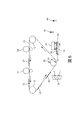
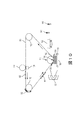
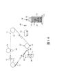
図2に示されるように、本願明細書における例示的な3次元(3D)プリンタは、他の要素のうち、ローラー112上に支持されたドラム又は中間転写ベルト(ITB)などの中間転写面110と、1つ以上の印刷要素(例えば、現像装置114)とを含む。図2において、物品118はプラテンであり、物品120は転写定着ヒータであり、物品122は定着ステーションであり、物品142は硬化ステーション(例えば、LED)であり、物品148は支持材料除去ステーションである。さらに、物品130は転写定着ニップであり、物品134及び136は、各現像層102の前縁及び後縁を示している。本願明細書における装置は、図2に示されるように、1つの現像装置のみを含むことができるか、又は、後述する図20に示されるように、多くを含むことができる。さらに、(表面又はベルトとすることができる)プラテン118は、ITB110に隣接している。この例において、プラテン118は、真空ベルトである。
As shown in FIG. 2, the exemplary three-dimensional (3D) printer herein includes an
図2は、(潜在的に乾燥した)粉末ポリマーワックス材料(例えば、帯電した3Dトナー)などの材料102をITB110に静電的に転写するように印刷要素116が配置されていることを示している。静電転写は、(例えば、電荷発生器128によって生成される)ベルトと転写される材料102との電荷差によって生じる。要素102は、時には「現像層」と称されることもある。現像層102は、ITB110の別個の領域上にあり、均一な矩形とすることができるか、又は、その層(及びその関連する支持要素)における3D構造の要素に対応するパターンとすることができる。
FIG. 2 shows that the
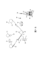
図3に示されるように、転写定着ステーション130は、ITB110に隣接している。転写定着ステーション130は、ITB110の一方側において、ITB110を支持するローラー112を含む。転写定着ステーション130は、ITB110が転写定着ステーション130へと移動するのにともない層102を受けるように配置されている。より具体的には、材料現像ステーション114及び転写定着ステーション130は、ITB110がプロセス方向に移動しているときに、ITB110上の層102が材料現像ステーション114を最初に通過した後に転写定着ステーション130を通過するようにITB110に対して配置されている。
As shown in FIG. 3, the
したがって、現像装置114によってITB上に印刷される材料は、所定長を有する現像層102を形成する。同様に、図3に示されるように、現像層102のそれぞれは、ITB110が移動している(ITB110の隣にある矢印によって示されている)プロセス方向に向かって配向された前縁134と、前縁134に対向する後縁136とを有する。
Therefore, the material printed on the ITB by the developing
図3における垂直矢印によって示されるように、プラテン118は、プラテン118がITB110とするように((全て一般に物品118によって示される)モータ、ギア、プーリ、ケーブル、ガイドなどを使用して)ITB110に向かって移動する。現像層102及びITB110は、転写前に現像層102を「粘着性」状態(すなわち、ガラス転移温度(Tg)よりも高いがトナー樹脂の溶融又は融解温度Tmよりも低い温度まで)にするように、ヒータ120によって局部的に加熱される。プラテン118はまた、ヒータ120によってほぼ同じ温度まで加熱された後、ITB−プラテンニップ(転写定着ニップ130)を通って平行移動する際に粘着層102と同期して接触される。それにより、ITB110は、プラテン118上の造形材料102及び支持材料105の現像層102を連続的に形成するように、プラテン118がITB110に接触するたびに、造形材料102及び支持材料105の現像層102の1つをプラテン118に転写する。
As indicated by the vertical arrows in FIG. 3, the
より具体的には、図3に示されるように、転写ニップ130において、転写ニップ130内の現像層102の前縁134は、プラテン118の対応する位置に転写され始める。それゆえに、プラテン118は、現像層102の前縁134が転写ニップ130のローラーの最低位置にある位置においてITB110上の現像層102と接触するように移動する。この例において、現像層102の後縁136は、まだ転写ニップ130に到達しておらず、したがって、まだプラテン118に転写されていない。
More specifically, as shown in FIG. 3, in the transfer nip 130, the
図4に示されるように、プラテン118は、現像層102が汚れなくプラテン118上に清浄に転写するのを可能とするように、プラテン真空ベルトを移動又は回転させることによってITB110と同期して移動する(ITB110と同じ速度及び同じ方向に移動する)。図4において、現像層102の後縁136は、まだ転写ニップ130に到達しておらず、したがってプラテン118に転写されていない唯一の部分である。そして、ITB110がプロセス方向に移動するのにともない、プラテン118は、現像層102の後縁136が転写ニップ130のローラーの底部に到達するまで、ITB110と同じ速度及び同じ方向に移動し、その時点で、プラテン118は、図5に示されるように、ITB110から離れ、定着ステーション122へと移動する。
As shown in FIG. 4, the
図5において、プラテン118は、加熱された加圧ローラー122を含むことができる定着ステーション120へと移動する。図6に示されるように、プラテン118は、加圧ローラーの回転に同期して移動し、現像層102をプラテン118(又はプラテン118上に存在する以前に転写された層102)に結合するように加熱及び加圧する。これらのプラテン118とITB110(及び加圧ローラー)との間の同期移動は、現像装置114及び116によって印刷された支持及び造形材料のパターン(102)を歪み又は汚れなしでITB110からプラテン118に正確に転写させる。
In FIG. 5, the
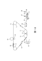
図7に示されるように、定着ステーション122は、転写定着ステーション130と硬化ステーション142との間に配置されている。転写定着ステーション130、定着ステーション122及び硬化ステーション142は、プラテン118が転写定着ステーション130を最初に通過した後に定着ステーション122を通過し、そして硬化ステーション142を通過するように、プラテン118に対して配置されている。それゆえに、発光ダイオード(LED)硬化ステーション142は、各層が定着ステーション122において定着された直後に各層102の異なる部分にLED紫外光を選択的に印加するように配置されている。プラテン118は、現像層102のそれぞれを独立して硬化させて各現像層102をプラテン118、プラテン118上に既に定着された任意の以前に転写された現像層102に連続的に接合するように、ITB110が現像層102のそれぞれをプラテン118に転写した後(及びそのような層のそれぞれが定着ステーション122において定着された後)に硬化ステーション142へと移動する。
As shown in FIG. 7, the fixing
LED硬化ステーション142は、造形材料となる層102の一部におけるポリマーを一体に架橋するように、層102にLED紫外光146を選択的に印加する。しかしながら、LED硬化ステーションは、支持材料となる層の第2の部分にLED紫外光を印加しない。それゆえに、LED紫外光は、未架橋材料として支持材料を残すように支持材料におけるポリマーを架橋することなく造形材料の一部におけるポリマーを一体に架橋する。
The
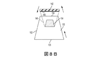
図8A〜図8Bは、硬化ステーション142において処理される層102の1つを示している。より具体的には、図8Aにおいて、単一点光源UV LED素子142は、材料層102の均一領域の異なる領域を指向的に露光することができる一方で、図8Bにおいて、UV LED素子142は、同様に異なる領域を選択的に露光するアレイ素子である。2つの構成が示されているが、当業者は、物品142が他の部分(105)を照射することなく層102の特定の部分(104)を選択的に照射するようにアドレス指定可能なパターンでUV波長光を提供するLED光の任意の形態であることを理解するであろう。
8A-8B show one of the
例えば、図8Aに示される単一点LED142は、(レンズ、プリズムなど143を使用して)UV光の集束点を提供し、LED142は、層が静止している又は移動しているときに層102の異なる部分にUV光の集束点を向けるように(矢印によって示されるように)回転させ、それにより、層102の選択された部分にのみUV放射線を供給するように、モータ、ギア(その全ては、物品142によって概略的に示される)などを含む。
For example, the
図8Bに示される他の例において、LED142は、複数のLED145の全幅アレイとして示されている。アレイ142は、層102と少なくとも同じ幅とすることができ、アレイ142は、層の幅にわたって(例えば、平行に)配置された細長構造であり、アレイ142は、層102の幅に愛して垂直な方向に移動する。それゆえに、LEDのアレイ142は、LED145のうちの選択されたものが照射するときに(矢印によって示されるように)比較的層102の前縁から後縁まで移動し、このプロセスにより、LEDのアレイ142は、層102の選択された部分に対してUV放射線を供給するのみである。LEDのアレイ142は、モータ及びギア(その全ては、物品142によって概略的に示されている)を使用して移動することができるか、又は、LEDのアレイ142は静止することができ、層102を含むプラテン118は、アレイ142における個々のLED145のそれぞれが照射するのにともない、LEDのアレイ142によって層102を通過することができる。当業者は、図8A及び図8Bが層102のうちの選択された部分(104)にUV放射線をアドレス指定可能に供給するためにLEDが使用されることができる2つの方法を示していることを理解するであろう。
In another example shown in FIG. 8B,
したがって、図8A及び図8Bの双方において、LED紫外光146は、材料102の一部を硬化させてそれを造形材料104に変性し、LED紫外光146を層102の他の部分に供給しない(これらの非硬化部分は、支持材料が層102の材料と同じであっても、そのようなものを硬化された造形材料104と区別するために時には「支持材料105」と称される)。それゆえに、LED紫外光146は、未架橋溶融材料として支持材料105を残すように未露光支持材料105におけるポリマーを架橋することなく材料104の露光部分におけるポリマーを架橋する。同様に、造形材料104及び支持材料105のこれらの部分は、同じ溶融層102の異なる部分である。
Thus, in both FIG. 8A and FIG. 8B, the
硬化プロセスに関して、材料102は、それらのガラス転移温度とそれらの溶融温度との間の温度までそのような材料102を加熱して、その形状又はパターンに影響を及ぼすことなく材料102を1つに接合することによって(完全に溶融されることなく)硬化されることができ、それにより、堅い構造を形成する。それゆえに、本願明細書における方法及び装置により、プラテンは、層102が著しく冷却される前に且つ層102が依然としてガラス転移温度と溶融温度の間にある間に硬化ステーション142へと移動する。
With respect to the curing process,
当業者は、造形及び支持材料の選択が硬化ステーション142によって行われる硬化プロセスの種類によって調整されることを理解するであろう。さらに、他の硬化処理及び要素が使用可能であり、上述したことは、1つの限定的な例としてのみ提示されるにすぎず、本願明細書における装置及び方法は、現在知られているか又は将来開発されるかにかかわらず、そのような方法及び要素の全てに適用可能である。さらに、そのような処理において、プラテン118は、(潜在的に冷却されて除湿された)吹き付け空気を供給する冷却ステーションへと移動することができ、又は、プラテン118は、次の処理ステップに移動する前に層102を冷却するのを可能とするように一時停止することができる。
One skilled in the art will appreciate that the shaping and selection of support materials is governed by the type of curing process performed by the curing
図9に示されるように、複数の現像層102におけるポリマーを積層106に架橋するために図2〜図7における処理が繰り返される。定着ステーション122は、各現像層102内の材料を一体に定着し、また、直近にプラテン118に転写された直接隣接した(例えば、プラテン118上で互いに接触する層102を接合する)現像層102に各現像層102を定着する。現像層102の積層106が成長するのにともない、追加の現像層102は、積層106の上部に形成される(図10)。図11に示されるように、そのような追加の現像層102は、定着ステーション122によって一体に定着される。図12において、硬化ステーション142は、積層106の最上層102のみにおけるポリマーを架橋するように最上層の部分のみを選択的に硬化させる。
As shown in FIG. 9, the processes in FIGS. 2-7 are repeated to crosslink the polymer in the plurality of
図13は、全ての層102が転写、定着及び硬化された後に積層106の全体が完全に形成されることを示している。さらに、図13は、独立した積層106の堆積内の支持材料105及び造形材料104の部分を示すオーバーレイを示している。そのようなものは、視認可能であってもなくてもよく、そのような造形及び支持材料が配置されることができる1つの例示的な方法を示すために図示されているにすぎない。
FIG. 13 shows that the
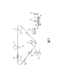
独立した積層106の3D構造は、外部溶媒浴などを使用して支持材料105を手動除去するのを可能とするように出力されることができ、又は、図14〜図16に示されるように自動処理が進められることができる。より具体的には、図14に示されるように、支持材料除去ステーション148は、プラテン118上の現在硬化された3Dの独立した積層106を受けられるように配置されている。支持材料除去ステーション148は、溶媒、水など156を加える。支持材料除去ステーション148によって加えられる任意の溶媒156は、造形材料104に影響を及ぼすことなく支持材料105を溶解するように選択される。同様に、上述したように、利用される溶媒は、造形材料104及び支持材料105の化学構成に依存する。図15は、支持材料105の約半分が残っており、造形材料104の一部が支持材料105の残りの積層から突出する処理を示している。図16は、支持材料除去ステーション148が全ての支持材料105を溶解又は除去した後に、造形材料104のみを残し、造形材料104のみから構成された完成した3D構造を残す処理を示している。
The 3D structure of the
図17及び図18は、図1に示される転写ニップ130の代わりに平面転写定着ステーション138を含む本願明細書における代替的な3D静電印刷構造を示している。図17に示されるように、平面転写定着ステーション138は、ローラー112の間にあり且つプラテン118に平行なITB110の平面部である。図18に示されるように、この構造により、プラテン118が平面転写定着ステーション138に接触するように移動すると、現像層102の全てがプラテン118又は部分的に形成された積層106に同時に転写され、図3及び図4に示される回転転写プロセスを回避する。あるいは、図19に示されるように、ドラム158は、ITB110の代わりに使用されることができ、他の全ての要素は、本願明細書において記載されるように動作する。それゆえに、ドラム158は、上述したように、現像ステーション114からの材料を受ける中間転写面とすることができるか、又は、感光体とすることができ、電荷の潜像を維持して現像装置254からの材料を受けることによって後述する感光体256として動作することができる。
17 and 18 illustrate an alternative 3D electrostatic printing structure herein that includes a flat
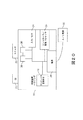
図20は、本願明細書における3Dプリンタ構造204の多くの構成を示している。3D印刷装置204は、コントローラ/有形プロセッサ224と、有形プロセッサ224及び印刷装置204の外部のコンピュータ化ネットワークに動作可能に接続された通信ポート(入力/出力)214とを含む。また、印刷装置204は、グラフィカルユーザインターフェース(GUI)アセンブリ212などの少なくとも1つのアクセサリ機能要素を含む。ユーザは、グラフィカルユーザインターフェース又はコントロールパネル212から、メッセージ、命令及びメニューオプションを受信し、グラフィカルユーザインターフェース又はコントロールパネル212を介して命令を入力することができる。
FIG. 20 shows many configurations of the
入力/出力装置214は、3D印刷装置204との間の通信に使用され、(現在知られているか又は将来開発されるかにかかわらず、任意の形態の)有線装置又は無線装置を備える。有形プロセッサ224は、印刷装置204の様々な動作を制御する。(光、磁気、コンデンサベースなどとすることができ、一時的信号とは異なる)持続性有形コンピュータ記憶媒体装置210は、有形プロセッサ224によって読み取り可能であり、コンピュータ化装置が本願明細書に記載されたものなどの様々な機能を実行するのを可能とするように有形プロセッサ224が実行する命令を記憶する。それゆえに、図20に示されるように、本体ハウジングは、電源218によって交流(AC)電源220から供給される電力で動作する1つ以上の機能部品を有する。電源218は、一般的な電力変換ユニット、電力貯蔵素子(例えば、電池など)などを含むことができる。
The input /
3D印刷装置204は、上述したようにプラテン上に造形及び支持材料の連続層を堆積させる少なくとも1つのマーキング装置(印刷エンジン)240を含み、専用画像プロセッサ224(すなわち、画像データの処理に特化されていることから汎用コンピュータとは異なる)に動作可能に接続されている。また、印刷装置204は、(電源218を介して)外部電源220から供給される電力において同様に動作する(スキャナ232などの)少なくとも1つのアクセサリ機能要素を含むことができる。
The
1つ以上の印刷エンジン240は、現在知られているか又は将来開発されるかにかかわらず、造形及び支持材料(トナーなど)を塗布する任意のマーキング装置を示すように意図されており、例えば、(図21に示されるような)中間転写ベルト110を使用する装置を含むことができる。
One or
それゆえに、図21に示されるように、図20に示される印刷エンジン240のそれぞれは、1つ以上の潜在的に異なる(例えば、異なる色、異なる材料など)造形材料現像ステーション152〜158、1つ以上の潜在的に異なる(例えば、異なる色、異なる材料など)支持材料現像ステーションなどを利用することができる。現像ステーション152〜158は、個々の静電マーキングステーション、個々のインクジェットステーション、個々のドライインクステーションなど、現在知られているか又は将来開発される任意の形態の現像ステーションとすることができる。現像ステーション152〜158のそれぞれは、(中間転写ベルト110の状態とは潜在的に無関係に)単一ベルト回転の間に連続して中間転写ベルト110の同じ位置に材料のパターンを転写し、それにより、十分且つ完全な画像が中間転写ベルト110に転写される前に中間転写ベルト110が通過しなければならない回数を低減させる。
Therefore, as shown in FIG. 21, each of the
それゆえに、図21は、異なる色の材料を中間転写ベルト(ITB110)に静電的に転写するように配置された異なる色の現像ステーション152〜158を示している。例えば、それぞれ異なる現像ステーション152〜158は、他の現像ステーション152〜158によって供給される材料の色とは異なる材料の色を供給することができる。図21は、回転ベルト(110)に隣接又は接触する4つの現像ステーションを示しているが、当業者によって理解されるように、そのような装置は、任意数のマーキングステーション(例えば、1、2、3、5、8、11など)を使用することができる。 Therefore, FIG. 21 shows different color development stations 152-158 arranged to electrostatically transfer different color materials to the intermediate transfer belt (ITB 110). For example, each different development station 152-158 may supply a material color that is different from the material color supplied by the other development stations 152-158. Although FIG. 21 shows four development stations adjacent to or in contact with the rotating belt (110), as will be appreciated by those skilled in the art, such an apparatus can include any number of marking stations (eg, 1, 2). 3, 5, 8, 11, etc.) can be used.
中間転写ベルト110に隣接して(又は潜在的に接触して)配置された1つの例示的な個々の静電現像ステーション114が図22に示されている。個々の静電現像ステーション114のそれぞれは、内部感光体256上に均一な電荷を形成する独自の帯電ステーション258と、帯電潜像に均一な電荷をパターン形成する内部露光装置260と、帯電潜像に適合するパターンで感光体256に造形又は支持材料を転写する内部現像装置254とを含む。そして、造形又は支持材料のパターンは、造形又は支持材料の電荷に対する中間転写ベルト110の逆電荷、すなわち中間転写ベルト110の反対側において電荷発生器128によって通常生成される電荷によって感光体256から中間転写ベルト110へと引き込まれる。
One exemplary individual
UV硬化性トナーは、樹脂骨格構造、隣接するポリマー鎖を一体に結合する任意の架橋剤及びUV光開始剤においてエチレン性不飽和(二重結合)を有する樹脂を含む。時には、トナー樹脂のポリマー骨格が隣接するポリマー骨格によって所望の架橋を達成することができるエチレン性不飽和を含有することから、架橋剤は省略される。これにかかわらず、所望であれば、様々な高温安定架橋剤はまた、材料トナー樹脂102に組み込まれることができる。
The UV curable toner includes a resin backbone structure, an optional crosslinker that bonds adjacent polymer chains together, and a resin having ethylenic unsaturation (double bonds) in the UV photoinitiator. Sometimes the crosslinker is omitted because the polymer backbone of the toner resin contains ethylenic unsaturation that can achieve the desired crosslinking by the adjacent polymer backbone. Regardless, various high temperature stable crosslinkers can also be incorporated into the
米国特許第8,488,994号明細書に示されるように、電子写真法を使用した3D部品を印刷するための積層造形システムが知られている。このシステムは、表面を有する感光体要素と、感光体要素の表面上に材料の層を現像するように構成された現像ステーションとを含む。このシステムはまた、回転可能な感光体要素の表面から現像層を受けるように構成された転写媒体と、受けた層の少なくとも一部から3D部品を印刷するために層毎に転写要素から現像層を受けるように構成されるプラテンとを含む。 As shown in US Pat. No. 8,488,994, an additive manufacturing system for printing 3D parts using electrophotography is known. The system includes a photoreceptor element having a surface and a development station configured to develop a layer of material on the surface of the photoreceptor element. The system also includes a transfer medium configured to receive a development layer from the surface of the rotatable photoreceptor element and a transfer element from the transfer element layer by layer to print a 3D part from at least a portion of the received layer. And a platen configured to receive.
米国特許第7,250,238号明細書に開示されるようなUV硬化性トナーに関して、印刷プロセスにおいてUV硬化性トナー組成物を利用する方法と同様にUV硬化性トナー組成物を提供することが知られている。米国特許第7,250,238号明細書は、実施形態において約100nmから約400nmのUV光などのUV放射線にさらすことによって硬化可能なトナーの生成を可能とする様々なトナーエマルジョン凝集プロセスを開示している。米国特許第7,250,238号明細書において、生成されたトナー組成物は、温度感受性包装及びホイルシールの製造などの様々な印刷用途において利用されることができる。米国特許第7,250,238号明細書において、実施形態は、任意の着色剤、任意のワックス、スチレンから生成されるポリマー、並びに、ブチルアクリレート、カルボキシエチルアクリレート及びUV光硬化性アクリレートオリゴマーからなる群から選択されるアクリレートを含むUV硬化性トナー組成物に関する。さらに、これらの態様は、顔料、任意のワックス、及びUV硬化性脂環式エポキシドから生成されたポリマーなどの着色剤からなるトナー組成物に関する。 For UV curable toners as disclosed in US Pat. No. 7,250,238, providing a UV curable toner composition as well as a method of utilizing the UV curable toner composition in a printing process. Are known. US Pat. No. 7,250,238 discloses various toner emulsion aggregation processes that, in embodiments, enable the production of curable toners by exposure to UV radiation, such as UV light from about 100 nm to about 400 nm. doing. In US Pat. No. 7,250,238, the toner composition produced can be utilized in a variety of printing applications, such as the manufacture of temperature sensitive packaging and foil seals. In US Pat. No. 7,250,238, embodiments consist of optional colorants, optional waxes, polymers formed from styrene, and butyl acrylate, carboxyethyl acrylate and UV light curable oligomers. It relates to a UV curable toner composition comprising an acrylate selected from the group. Furthermore, these embodiments relate to toner compositions comprising pigments, optional waxes, and colorants such as polymers made from UV curable cycloaliphatic epoxides.
さらに、米国特許第7,250,238号明細書は、スチレン、ブチルアクリレート、カルボキシエチルアクリレート、及びUV硬化アクリレートから形成されるポリマーを含有するラテックスを着色剤及びワックスと混合することと、必要に応じて第2の混合物に分散されたトナー前駆体粒子の凝集及び形成を引き起こすようにこの混合物に凝集剤を添加することと、トナー粒子を形成するためにポリマーのガラス転移温度(Tg)以上の温度までトナー前駆体粒子を加熱することと、必要に応じてトナー粒子を洗浄することと、必要に応じてトナー粒子を乾燥させることとを含むUV硬化性トナー組成物を形成する方法を開示している。さらなる態様は、この方法によって製造されたトナー粒子に関する。 In addition, US Pat. No. 7,250,238 discloses mixing a latex containing a polymer formed from styrene, butyl acrylate, carboxyethyl acrylate, and UV cured acrylate with a colorant and a wax, and Accordingly adding an aggregating agent to the mixture to cause aggregation and formation of toner precursor particles dispersed in the second mixture, and a polymer glass transition temperature (Tg) or higher to form toner particles. Disclosed is a method of forming a UV curable toner composition comprising heating toner precursor particles to a temperature, washing the toner particles as needed, and drying the toner particles as needed. ing. A further aspect relates to toner particles made by this method.
いくつかの例示的な構造が添付図面に示されているが、当業者は、図面は簡略化された概略図であり、以下に提示される特許請求の範囲は図示されていない(又は潜在的に多くはない)がそのような装置及びシステムとともに一般的に利用されるより多くの特徴を包含することを理解するであろう。したがって、特許出願人は、以下に提示される特許請求の範囲が添付図面によって限定されることを意図しておらず、代わりに、添付図面は、特許請求された特徴が実施されることができるいくつかの方法を例示するために提供されるにすぎない。 Although some exemplary structures are shown in the accompanying drawings, those skilled in the art will appreciate that the drawings are simplified schematics and that the claims presented below are not illustrated (or potentially Will be understood to encompass more features commonly used with such devices and systems. Accordingly, the Applicant does not intend the scope of the claims presented below to be limited by the accompanying drawings, but instead the appended drawings may embody the claimed features. It is only provided to illustrate some methods.
多くのコンピュータ化された装置が上述されている。チップベースの中央処理装置(CPU)と、(グラフィックユーザインターフェース(GUI)、メモリ、コンパレータ、有形プロセッサなどを含む)入力/出力装置とを含むコンピュータ化装置は、米国テキサス州ラウンドロックのデルコンピュータ及び米国カリフォルニア州クパチーノのアップルコンピュータ社などの製造業者によって製造された周知且つ容易に入手可能な装置である。そのようなコンピュータ化装置は、一般に、入力/出力装置、電源、有形プロセッサ、電子記憶メモリ、配線などを含み、読者が本願明細書に記載されるシステム及び方法の顕著な態様にフォーカスするのを可能とするように、その詳細は本願明細書から省略されている。同様に、プリンタ、複写機、スキャナ及び他の類似の周辺機器は、米国コネチカット州ノーウォークのゼロックス社から入手可能であり、そのような装置の詳細は、簡潔性及び読者のフォーカスの目的のために本願明細書においては記載されない。 A number of computerized devices have been described above. A computerized device including a chip-based central processing unit (CPU) and input / output devices (including a graphic user interface (GUI), memory, comparators, tangible processors, etc.) includes a Dell computer in Round Rock, Texas, USA A well-known and readily available device manufactured by a manufacturer such as Apple Computer Corporation of Cupertino, California, USA. Such computerized devices generally include input / output devices, power supplies, tangible processors, electronic storage memory, wiring, etc. to help the reader focus on the salient aspects of the systems and methods described herein. The details have been omitted from the present specification to allow. Similarly, printers, copiers, scanners and other similar peripherals are available from Xerox Corporation of Norwalk, Connecticut, USA, and details of such devices are for purposes of brevity and reader focus. Are not described herein.
本願明細書において使用されるプリンタ又は印刷装置という用語は、任意の目的のために印刷出力機能を実行するディジタル複写機、製本機、ファクシミリ装置、複合機などの任意の装置を包含する。プリンタや印刷エンジンなどの詳細は周知であり、提示された顕著な特徴にフォーカスされた本開示を維持するために本願明細書においては詳細に記載されない。本願明細書におけるシステム及び方法は、カラー、モノクロで印刷する又はカラー若しくはモノクロ画像データを処理するシステム及び方法を包含することができる。全ての上述したシステム及び方法は、静電及び/又は電子写真装置及び/又はプロセスに特に適用可能である。 As used herein, the term printer or printing device encompasses any device such as a digital copier, bookbinding machine, facsimile machine, multifunction device, etc. that performs a print output function for any purpose. Details such as printers and print engines are well known and are not described in detail herein to maintain this disclosure focused on the salient features presented. The systems and methods herein can include systems and methods that print in color, monochrome, or process color or monochrome image data. All the systems and methods described above are particularly applicable to electrostatic and / or electrophotographic apparatus and / or processes.
本発明の目的のために、定着という用語は、乾燥、硬化、重合、架橋、結合、又は付加反応若しくはコーティングの他の反応を意味する。さらに、本願明細書において使用される「右(right)」、「左(left)」、「垂直(vertical)」、「水平(horizontal)」、「上部(top)」、「底部(bottom)」、「上(upper)」、「下(lower)」、「下方(under)」、「下(below)」、「下層(underlying)」、「上(over)」、「上層(overlying)」、「平行(parallel)」、「垂直(perpendicular)」などの用語は、(特に断らない限り)それらが図面において配向及び図示されるように相対的位置であると理解される。「接触(touching)」、「上(on)」、「直接接触(in direct contact)」、「当接(abutting)」、「直接隣接(directly adjacent to)」などの用語は、少なくとも1つの要素が(記載された要素を分離する他の要素なしで)他の要素に物理的に接触することを意味する。さらに、自動化又は自動的にという用語は、(機械又はユーザによって)処理が開始されると、1つ以上の機械がユーザからのさらなる入力なしで処理を行うことを意味する。本願明細書における図面において、同一の識別符号は、同一又は類似の項目を識別する。 For the purposes of the present invention, the term fixing means drying, curing, polymerization, crosslinking, bonding, or addition reactions or other reactions of the coating. Further, as used herein, “right”, “left”, “vertical”, “horizontal”, “top”, “bottom” , “Upper”, “lower”, “under”, “below”, “underlying”, “over”, “overlying”, Terms such as “parallel”, “perpendicular” and the like are understood to be relative positions as they are oriented and illustrated in the drawings (unless otherwise noted). Terms such as “touching”, “on”, “in direct contact”, “butting”, “directly adjunct to” and the like are at least one element Means in physical contact with other elements (without other elements separating the described elements). Furthermore, the term automated or automatically means that one or more machines perform processing without further input from the user when processing is initiated (by the machine or user). In the drawings in this specification, the same identification symbols identify the same or similar items.
上記開示された及び他の特徴及び機能又はその代替例は、多くの他の異なるシステム又は用途に望ましくは組み合わせることができることが理解されるであろう。様々な現在予見できない又は予測されない代替例、変更例、変形例又は改良は、当業者によって後に行われることができ、以下の特許請求の範囲に包含されるようにも意図される。特定の請求項自体に具体的に定義されない限り、本願明細書におけるシステム及び方法のステップ又は構成要素は、任意の特定の順序、数、位置、大きさ、形状、角度、色又は材料に対する限定として任意の上記例から暗示又は取り込まれることはできない。 It will be appreciated that the above-disclosed and other features and functions or alternatives thereof may be desirably combined with many other different systems or applications. Various alternatives, modifications, variations or improvements that are not currently foreseen or anticipated can be made later by those skilled in the art and are also intended to be encompassed by the following claims. Unless specifically defined in the specific claims themselves, the steps or components of the systems and methods herein are intended as limitations on any particular order, number, location, size, shape, angle, color or material. It cannot be implied or taken from any of the above examples.
Claims (10)
中間転写面と、
材料の層を前記中間転写面に静電的に転写するように配置された現像ステーションと、
前記中間転写面に隣接する転写定着ステーションと、
前記中間転写面に対して移動するプラテンであって、前記プラテン上の前記層の独立した積層を連続的に形成するように前記転写定着ステーションにおいて前記中間転写面上の前記層の1つに前記プラテンが接触するたびに、前記中間転写面が前記材料の層を前記プラテンに転写するプラテンと、
前記層が前記転写定着ステーションから前記プラテンに転写された後に前記層に紫外光を印加するように配置された硬化ステーションであって、前記層内の前記材料の一部のみにおけるポリマーを架橋させるように前記紫外光を選択的に印加する硬化ステーションと
を備える、3Dプリンタ。 In a three-dimensional (3D) printer,
An intermediate transfer surface;
A development station arranged to electrostatically transfer a layer of material to the intermediate transfer surface;
A transfer fixing station adjacent to the intermediate transfer surface;
A platen that moves relative to the intermediate transfer surface, wherein the one of the layers on the intermediate transfer surface in the transfer fixing station so as to continuously form an independent stack of the layers on the platen; A platen where the intermediate transfer surface transfers the layer of material to the platen each time the platen contacts;
A curing station arranged to apply ultraviolet light to the layer after the layer has been transferred from the transfer-fixing station to the platen so as to crosslink the polymer in only a portion of the material in the layer. And a curing station that selectively applies the ultraviolet light.
前記3Dプリンタが、さらに、前記第2の部分から前記一部を分離して3D印刷された部品を残すために前記第2の部分を除去するように配置された材料除去ステーションを備える、請求項1に記載の3Dプリンタ。 The curing station does not apply the ultraviolet light to the second portion of the material in the layer;
The 3D printer further comprises a material removal station arranged to remove the second portion to separate the portion from the second portion and leave a 3D printed part. The 3D printer according to 1.
中間転写面と、
異なる材料の層を前記中間転写面に静電的に転写するように配置された現像ステーションと、
前記中間転写面に隣接する転写定着ステーションであって、前記中間転写面が前記転写定着ステーションを通過するのにともない前記層を受けるように配置された転写定着ステーションと、
前記中間転写面に対して移動するプラテンであって、前記プラテン上の前記層の独立した積層を連続的に形成するように前記転写定着ステーションにおいて前記中間転写面上の前記層の1つに前記プラテンが接触するたびに、前記中間転写面が前記異なる材料の層を前記プラテンに転写するプラテンと、
前記層が前記転写定着ステーションから前記プラテンに転写された後に前記層のそれぞれにLED紫外光を印加するように配置されたLED硬化ステーションであって、前記層内の前記異なる材料の一部のみにおけるポリマーを架橋させるように前記LED紫外光を前記層に選択的に印加するLED硬化ステーションと
を備える、3Dプリンタ。 In a three-dimensional (3D) printer,
An intermediate transfer surface;
A development station arranged to electrostatically transfer layers of different materials to the intermediate transfer surface;
A transfer fixing station adjacent to the intermediate transfer surface, the transfer fixing station arranged to receive the layer as the intermediate transfer surface passes through the transfer fixing station;
A platen that moves relative to the intermediate transfer surface, wherein the one of the layers on the intermediate transfer surface in the transfer fixing station so as to continuously form an independent stack of the layers on the platen; A platen on which the intermediate transfer surface transfers the layer of different material to the platen each time the platen contacts;
An LED curing station arranged to apply LED ultraviolet light to each of the layers after the layers have been transferred from the transfer-fixing station to the platen, in only a portion of the different materials in the layers A 3D printer comprising: an LED curing station that selectively applies the LED ultraviolet light to the layer to crosslink the polymer.
中間転写面と、
異なる材料の層を前記中間転写面に静電的に転写するように配置された現像ステーションと、
前記中間転写面に隣接する転写定着ステーションであって、前記中間転写面が前記転写定着ステーションを通過するのにともない前記層を受けるように配置された転写定着ステーションと、
前記中間転写面に対して移動するプラテンであって、前記プラテン上の前記層の独立した積層を連続的に形成するように前記転写定着ステーションにおいて前記中間転写面上の前記層の1つに前記プラテンが接触するたびに、前記中間転写面が前記異なる材料の層を前記プラテンに転写するプラテンと、
前記層が前記転写定着ステーションから前記プラテンに転写された後に前記層のそれぞれにLED紫外光を印加するように配置されたLED硬化ステーションであって、前記層内の前記異なる材料の一部のみにおけるポリマーを一体に架橋させるように前記LED紫外光を前記層に選択的に印加するLED硬化ステーションと
を備える、3Dプリンタ。 In a three-dimensional (3D) printer,
An intermediate transfer surface;
A development station arranged to electrostatically transfer layers of different materials to the intermediate transfer surface;
A transfer fixing station adjacent to the intermediate transfer surface, the transfer fixing station arranged to receive the layer as the intermediate transfer surface passes through the transfer fixing station;
A platen that moves relative to the intermediate transfer surface, wherein the one of the layers on the intermediate transfer surface in the transfer fixing station so as to continuously form an independent stack of the layers on the platen; A platen on which the intermediate transfer surface transfers the layer of different material to the platen each time the platen contacts;
An LED curing station arranged to apply LED ultraviolet light to each of the layers after the layers have been transferred from the transfer-fixing station to the platen, in only a portion of the different materials in the layers A 3D printer comprising: an LED curing station that selectively applies the LED ultraviolet light to the layer to crosslink the polymer together.
Applications Claiming Priority (2)
| Application Number | Priority Date | Filing Date | Title |
|---|---|---|---|
| US15/152,651 US10005227B2 (en) | 2016-05-12 | 2016-05-12 | Electrostatic 3-D printer using addressable UV crosslinking |
| US15/152,651 | 2016-05-12 |
Publications (3)
| Publication Number | Publication Date |
|---|---|
| JP2017206007A true JP2017206007A (en) | 2017-11-24 |
| JP2017206007A5 JP2017206007A5 (en) | 2020-06-11 |
| JP6785183B2 JP6785183B2 (en) | 2020-11-18 |
Family
ID=58671483
Family Applications (1)
| Application Number | Title | Priority Date | Filing Date |
|---|---|---|---|
| JP2017085356A Active JP6785183B2 (en) | 2016-05-12 | 2017-04-24 | Electrostatic 3D printer with addressable UV cross-linking |
Country Status (5)
| Country | Link |
|---|---|
| US (1) | US10005227B2 (en) |
| EP (1) | EP3243657B1 (en) |
| JP (1) | JP6785183B2 (en) |
| KR (1) | KR102142833B1 (en) |
| CN (1) | CN107364123B (en) |
Families Citing this family (2)
| Publication number | Priority date | Publication date | Assignee | Title |
|---|---|---|---|---|
| US11167375B2 (en) | 2018-08-10 | 2021-11-09 | The Research Foundation For The State University Of New York | Additive manufacturing processes and additively manufactured products |
| US11534959B2 (en) * | 2020-09-24 | 2022-12-27 | Inkbit, LLC | Delayed cure additive manufacturing |
Citations (6)
| Publication number | Priority date | Publication date | Assignee | Title |
|---|---|---|---|---|
| JP2011020842A (en) * | 2009-07-21 | 2011-02-03 | Fuji Xerox Co Ltd | Sheet length measuring device and image forming device |
| JP2014533210A (en) * | 2011-09-23 | 2014-12-11 | ストラタシス,インコーポレイテッド | Layer melt transfer for additive manufacturing. |
| US20150024169A1 (en) * | 2013-07-17 | 2015-01-22 | Stratasys, Inc. | Method for Printing 3D Parts and Support Structures with Electrophotography-Based Additive Manufacturing |
| WO2015092017A1 (en) * | 2013-12-20 | 2015-06-25 | Luxexcel Holding B.V. | Method for printing a three dimensional structure and apparatus therefore |
| JP2016193564A (en) * | 2015-04-01 | 2016-11-17 | 株式会社ミマキエンジニアリング | Method for manufacturing three-dimensional molded object |
| WO2016192626A1 (en) * | 2015-06-03 | 2016-12-08 | 珠海天威飞马打印耗材有限公司 | Three-dimensional rapid prototyping device and prototyping method |
Family Cites Families (20)
| Publication number | Priority date | Publication date | Assignee | Title |
|---|---|---|---|---|
| US7250238B2 (en) | 2003-12-23 | 2007-07-31 | Xerox Corporation | Toners and processes thereof |
| US7184698B2 (en) | 2004-03-17 | 2007-02-27 | Eastman Kodak Company | Durable electrophotographic prints |
| US7690782B2 (en) | 2004-12-07 | 2010-04-06 | Xerox Corporation | Apparatus and process for printing ultraviolet curable inks |
| US7270408B2 (en) | 2005-01-14 | 2007-09-18 | Xerox Corporation | Low level cure transfuse assist for printing with radiation curable ink |
| US7851549B2 (en) | 2007-12-13 | 2010-12-14 | Xerox Corporation | Curable polyester latex made by phase inversion emulsification |
| US8876513B2 (en) * | 2008-04-25 | 2014-11-04 | 3D Systems, Inc. | Selective deposition modeling using CW UV LED curing |
| US8470231B1 (en) | 2009-06-01 | 2013-06-25 | Stratasys Ltd. | Three-dimensional printing process for producing a self-destructible temporary structure |
| JP2011028055A (en) * | 2009-07-27 | 2011-02-10 | Fuji Xerox Co Ltd | Image forming method, process cartridge and image forming apparatus |
| US20130186558A1 (en) * | 2011-09-23 | 2013-07-25 | Stratasys, Inc. | Layer transfusion with heat capacitor belt for additive manufacturing |
| US8459280B2 (en) * | 2011-09-23 | 2013-06-11 | Stratasys, Inc. | Support structure removal system |
| US8488994B2 (en) | 2011-09-23 | 2013-07-16 | Stratasys, Inc. | Electrophotography-based additive manufacturing system with transfer-medium service loops |
| CN104781063B (en) | 2012-11-09 | 2018-02-27 | 赢创罗姆有限公司 | Purposes and preparation for the coated long filament of extruded type 3D printing method |
| WO2014072147A1 (en) | 2012-11-09 | 2014-05-15 | Evonik Industries Ag | Multicoloured extrusion-based 3d printing |
| EP3597398A1 (en) | 2013-03-12 | 2020-01-22 | Orange Maker, LLC | 3d printing using spiral buildup |
| JP6376831B2 (en) * | 2013-06-20 | 2018-08-22 | キヤノン株式会社 | Manufacturing method of structure |
| US9029058B2 (en) | 2013-07-17 | 2015-05-12 | Stratasys, Inc. | Soluble support material for electrophotography-based additive manufacturing |
| AU2014349268B2 (en) | 2013-11-14 | 2019-01-31 | Structo Pte. Ltd. | Additive manufacturing device and method |
| US10369743B2 (en) | 2013-11-18 | 2019-08-06 | San Draw Inc. | Color or multi-material three-dimensional (3D) printing |
| US9744730B2 (en) | 2013-11-22 | 2017-08-29 | Stratasys, Inc. | Magnetic platen assembly for additive manufacturing system |
| CN104298084A (en) * | 2014-10-22 | 2015-01-21 | 珠海天威飞马打印耗材有限公司 | Developing agent, three-dimensional printing machine and three-dimensional printing method |
-
2016
- 2016-05-12 US US15/152,651 patent/US10005227B2/en active Active
-
2017
- 2017-04-18 CN CN201710254572.6A patent/CN107364123B/en active Active
- 2017-04-20 KR KR1020170051053A patent/KR102142833B1/en active IP Right Grant
- 2017-04-24 JP JP2017085356A patent/JP6785183B2/en active Active
- 2017-05-04 EP EP17169601.6A patent/EP3243657B1/en active Active
Patent Citations (6)
| Publication number | Priority date | Publication date | Assignee | Title |
|---|---|---|---|---|
| JP2011020842A (en) * | 2009-07-21 | 2011-02-03 | Fuji Xerox Co Ltd | Sheet length measuring device and image forming device |
| JP2014533210A (en) * | 2011-09-23 | 2014-12-11 | ストラタシス,インコーポレイテッド | Layer melt transfer for additive manufacturing. |
| US20150024169A1 (en) * | 2013-07-17 | 2015-01-22 | Stratasys, Inc. | Method for Printing 3D Parts and Support Structures with Electrophotography-Based Additive Manufacturing |
| WO2015092017A1 (en) * | 2013-12-20 | 2015-06-25 | Luxexcel Holding B.V. | Method for printing a three dimensional structure and apparatus therefore |
| JP2016193564A (en) * | 2015-04-01 | 2016-11-17 | 株式会社ミマキエンジニアリング | Method for manufacturing three-dimensional molded object |
| WO2016192626A1 (en) * | 2015-06-03 | 2016-12-08 | 珠海天威飞马打印耗材有限公司 | Three-dimensional rapid prototyping device and prototyping method |
Also Published As
| Publication number | Publication date |
|---|---|
| EP3243657A1 (en) | 2017-11-15 |
| KR20170128083A (en) | 2017-11-22 |
| US10005227B2 (en) | 2018-06-26 |
| KR102142833B1 (en) | 2020-08-10 |
| CN107364123A (en) | 2017-11-21 |
| JP6785183B2 (en) | 2020-11-18 |
| EP3243657B1 (en) | 2019-01-09 |
| CN107364123B (en) | 2020-09-29 |
| US20170326795A1 (en) | 2017-11-16 |
Similar Documents
| Publication | Publication Date | Title |
|---|---|---|
| US11130282B2 (en) | Electrostatic 3-D development apparatus using cold fusing | |
| EP3255504B1 (en) | Electrostatic 3-d printer system using leveling material and mechanical planer | |
| CN107364122B (en) | Electrostatic three-dimensional developing device using materials with different melting points | |
| KR102154471B1 (en) | Electro-photographic 3-d printing using dissolvable paper | |
| JP2017193170A (en) | Electro-photographic 3-d printing using collapsible substrate | |
| JP2017206007A (en) | Electrostatic 3d printer using addressable uv crosslinking | |
| US10350828B2 (en) | 3-D printing using intermediate transfer belt and curable polymers | |
| US10213958B2 (en) | Electrostatic 3-D printing system having acoustic transfer and corotron |
Legal Events
| Date | Code | Title | Description |
|---|---|---|---|
| RD02 | Notification of acceptance of power of attorney |
Free format text: JAPANESE INTERMEDIATE CODE: A7422 Effective date: 20170502 |
|
| RD04 | Notification of resignation of power of attorney |
Free format text: JAPANESE INTERMEDIATE CODE: A7424 Effective date: 20170725 |
|
| A521 | Request for written amendment filed |
Free format text: JAPANESE INTERMEDIATE CODE: A523 Effective date: 20200415 |
|
| A621 | Written request for application examination |
Free format text: JAPANESE INTERMEDIATE CODE: A621 Effective date: 20200415 |
|
| A871 | Explanation of circumstances concerning accelerated examination |
Free format text: JAPANESE INTERMEDIATE CODE: A871 Effective date: 20200415 |
|
| A975 | Report on accelerated examination |
Free format text: JAPANESE INTERMEDIATE CODE: A971005 Effective date: 20200508 |
|
| A131 | Notification of reasons for refusal |
Free format text: JAPANESE INTERMEDIATE CODE: A131 Effective date: 20200616 |
|
| TRDD | Decision of grant or rejection written | ||
| A01 | Written decision to grant a patent or to grant a registration (utility model) |
Free format text: JAPANESE INTERMEDIATE CODE: A01 Effective date: 20200929 |
|
| A61 | First payment of annual fees (during grant procedure) |
Free format text: JAPANESE INTERMEDIATE CODE: A61 Effective date: 20201026 |
|
| R150 | Certificate of patent or registration of utility model |
Ref document number: 6785183 Country of ref document: JP Free format text: JAPANESE INTERMEDIATE CODE: R150 |
|
| R250 | Receipt of annual fees |
Free format text: JAPANESE INTERMEDIATE CODE: R250 |