EP3243657B1 - Electrostatic 3-d printer using addressable uv crosslinking - Google Patents
Electrostatic 3-d printer using addressable uv crosslinking Download PDFInfo
- Publication number
- EP3243657B1 EP3243657B1 EP17169601.6A EP17169601A EP3243657B1 EP 3243657 B1 EP3243657 B1 EP 3243657B1 EP 17169601 A EP17169601 A EP 17169601A EP 3243657 B1 EP3243657 B1 EP 3243657B1
- Authority
- EP
- European Patent Office
- Prior art keywords
- layer
- station
- platen
- intermediate transfer
- ultraviolet light
- Prior art date
- Legal status (The legal status is an assumption and is not a legal conclusion. Google has not performed a legal analysis and makes no representation as to the accuracy of the status listed.)
- Active
Links
Images


Classifications
-
- B—PERFORMING OPERATIONS; TRANSPORTING
- B29—WORKING OF PLASTICS; WORKING OF SUBSTANCES IN A PLASTIC STATE IN GENERAL
- B29C—SHAPING OR JOINING OF PLASTICS; SHAPING OF MATERIAL IN A PLASTIC STATE, NOT OTHERWISE PROVIDED FOR; AFTER-TREATMENT OF THE SHAPED PRODUCTS, e.g. REPAIRING
- B29C64/00—Additive manufacturing, i.e. manufacturing of three-dimensional [3D] objects by additive deposition, additive agglomeration or additive layering, e.g. by 3D printing, stereolithography or selective laser sintering
- B29C64/20—Apparatus for additive manufacturing; Details thereof or accessories therefor
- B29C64/205—Means for applying layers
- B29C64/209—Heads; Nozzles
-
- G—PHYSICS
- G03—PHOTOGRAPHY; CINEMATOGRAPHY; ANALOGOUS TECHNIQUES USING WAVES OTHER THAN OPTICAL WAVES; ELECTROGRAPHY; HOLOGRAPHY
- G03G—ELECTROGRAPHY; ELECTROPHOTOGRAPHY; MAGNETOGRAPHY
- G03G15/00—Apparatus for electrographic processes using a charge pattern
- G03G15/14—Apparatus for electrographic processes using a charge pattern for transferring a pattern to a second base
- G03G15/16—Apparatus for electrographic processes using a charge pattern for transferring a pattern to a second base of a toner pattern, e.g. a powder pattern, e.g. magnetic transfer
- G03G15/1605—Apparatus for electrographic processes using a charge pattern for transferring a pattern to a second base of a toner pattern, e.g. a powder pattern, e.g. magnetic transfer using at least one intermediate support
-
- B—PERFORMING OPERATIONS; TRANSPORTING
- B33—ADDITIVE MANUFACTURING TECHNOLOGY
- B33Y—ADDITIVE MANUFACTURING, i.e. MANUFACTURING OF THREE-DIMENSIONAL [3-D] OBJECTS BY ADDITIVE DEPOSITION, ADDITIVE AGGLOMERATION OR ADDITIVE LAYERING, e.g. BY 3-D PRINTING, STEREOLITHOGRAPHY OR SELECTIVE LASER SINTERING
- B33Y30/00—Apparatus for additive manufacturing; Details thereof or accessories therefor
-
- B—PERFORMING OPERATIONS; TRANSPORTING
- B29—WORKING OF PLASTICS; WORKING OF SUBSTANCES IN A PLASTIC STATE IN GENERAL
- B29C—SHAPING OR JOINING OF PLASTICS; SHAPING OF MATERIAL IN A PLASTIC STATE, NOT OTHERWISE PROVIDED FOR; AFTER-TREATMENT OF THE SHAPED PRODUCTS, e.g. REPAIRING
- B29C64/00—Additive manufacturing, i.e. manufacturing of three-dimensional [3D] objects by additive deposition, additive agglomeration or additive layering, e.g. by 3D printing, stereolithography or selective laser sintering
- B29C64/20—Apparatus for additive manufacturing; Details thereof or accessories therefor
- B29C64/245—Platforms or substrates
-
- B—PERFORMING OPERATIONS; TRANSPORTING
- B28—WORKING CEMENT, CLAY, OR STONE
- B28B—SHAPING CLAY OR OTHER CERAMIC COMPOSITIONS; SHAPING SLAG; SHAPING MIXTURES CONTAINING CEMENTITIOUS MATERIAL, e.g. PLASTER
- B28B1/00—Producing shaped prefabricated articles from the material
- B28B1/001—Rapid manufacturing of 3D objects by additive depositing, agglomerating or laminating of material
-
- B—PERFORMING OPERATIONS; TRANSPORTING
- B28—WORKING CEMENT, CLAY, OR STONE
- B28B—SHAPING CLAY OR OTHER CERAMIC COMPOSITIONS; SHAPING SLAG; SHAPING MIXTURES CONTAINING CEMENTITIOUS MATERIAL, e.g. PLASTER
- B28B11/00—Apparatus or processes for treating or working the shaped or preshaped articles
- B28B11/24—Apparatus or processes for treating or working the shaped or preshaped articles for curing, setting or hardening
- B28B11/243—Setting, e.g. drying, dehydrating or firing ceramic articles
-
- B—PERFORMING OPERATIONS; TRANSPORTING
- B29—WORKING OF PLASTICS; WORKING OF SUBSTANCES IN A PLASTIC STATE IN GENERAL
- B29C—SHAPING OR JOINING OF PLASTICS; SHAPING OF MATERIAL IN A PLASTIC STATE, NOT OTHERWISE PROVIDED FOR; AFTER-TREATMENT OF THE SHAPED PRODUCTS, e.g. REPAIRING
- B29C35/00—Heating, cooling or curing, e.g. crosslinking or vulcanising; Apparatus therefor
- B29C35/02—Heating or curing, e.g. crosslinking or vulcanizing during moulding, e.g. in a mould
- B29C35/08—Heating or curing, e.g. crosslinking or vulcanizing during moulding, e.g. in a mould by wave energy or particle radiation
- B29C35/0805—Heating or curing, e.g. crosslinking or vulcanizing during moulding, e.g. in a mould by wave energy or particle radiation using electromagnetic radiation
-
- B—PERFORMING OPERATIONS; TRANSPORTING
- B29—WORKING OF PLASTICS; WORKING OF SUBSTANCES IN A PLASTIC STATE IN GENERAL
- B29C—SHAPING OR JOINING OF PLASTICS; SHAPING OF MATERIAL IN A PLASTIC STATE, NOT OTHERWISE PROVIDED FOR; AFTER-TREATMENT OF THE SHAPED PRODUCTS, e.g. REPAIRING
- B29C64/00—Additive manufacturing, i.e. manufacturing of three-dimensional [3D] objects by additive deposition, additive agglomeration or additive layering, e.g. by 3D printing, stereolithography or selective laser sintering
- B29C64/10—Processes of additive manufacturing
- B29C64/141—Processes of additive manufacturing using only solid materials
-
- B—PERFORMING OPERATIONS; TRANSPORTING
- B29—WORKING OF PLASTICS; WORKING OF SUBSTANCES IN A PLASTIC STATE IN GENERAL
- B29C—SHAPING OR JOINING OF PLASTICS; SHAPING OF MATERIAL IN A PLASTIC STATE, NOT OTHERWISE PROVIDED FOR; AFTER-TREATMENT OF THE SHAPED PRODUCTS, e.g. REPAIRING
- B29C64/00—Additive manufacturing, i.e. manufacturing of three-dimensional [3D] objects by additive deposition, additive agglomeration or additive layering, e.g. by 3D printing, stereolithography or selective laser sintering
- B29C64/20—Apparatus for additive manufacturing; Details thereof or accessories therefor
- B29C64/205—Means for applying layers
- B29C64/223—Foils or films, e.g. for transferring layers of building material from one working station to another
-
- B—PERFORMING OPERATIONS; TRANSPORTING
- B29—WORKING OF PLASTICS; WORKING OF SUBSTANCES IN A PLASTIC STATE IN GENERAL
- B29C—SHAPING OR JOINING OF PLASTICS; SHAPING OF MATERIAL IN A PLASTIC STATE, NOT OTHERWISE PROVIDED FOR; AFTER-TREATMENT OF THE SHAPED PRODUCTS, e.g. REPAIRING
- B29C64/00—Additive manufacturing, i.e. manufacturing of three-dimensional [3D] objects by additive deposition, additive agglomeration or additive layering, e.g. by 3D printing, stereolithography or selective laser sintering
- B29C64/20—Apparatus for additive manufacturing; Details thereof or accessories therefor
- B29C64/264—Arrangements for irradiation
-
- B—PERFORMING OPERATIONS; TRANSPORTING
- B29—WORKING OF PLASTICS; WORKING OF SUBSTANCES IN A PLASTIC STATE IN GENERAL
- B29C—SHAPING OR JOINING OF PLASTICS; SHAPING OF MATERIAL IN A PLASTIC STATE, NOT OTHERWISE PROVIDED FOR; AFTER-TREATMENT OF THE SHAPED PRODUCTS, e.g. REPAIRING
- B29C64/00—Additive manufacturing, i.e. manufacturing of three-dimensional [3D] objects by additive deposition, additive agglomeration or additive layering, e.g. by 3D printing, stereolithography or selective laser sintering
- B29C64/30—Auxiliary operations or equipment
- B29C64/307—Handling of material to be used in additive manufacturing
- B29C64/321—Feeding
-
- B—PERFORMING OPERATIONS; TRANSPORTING
- B29—WORKING OF PLASTICS; WORKING OF SUBSTANCES IN A PLASTIC STATE IN GENERAL
- B29C—SHAPING OR JOINING OF PLASTICS; SHAPING OF MATERIAL IN A PLASTIC STATE, NOT OTHERWISE PROVIDED FOR; AFTER-TREATMENT OF THE SHAPED PRODUCTS, e.g. REPAIRING
- B29C64/00—Additive manufacturing, i.e. manufacturing of three-dimensional [3D] objects by additive deposition, additive agglomeration or additive layering, e.g. by 3D printing, stereolithography or selective laser sintering
- B29C64/40—Structures for supporting 3D objects during manufacture and intended to be sacrificed after completion thereof
-
- B—PERFORMING OPERATIONS; TRANSPORTING
- B33—ADDITIVE MANUFACTURING TECHNOLOGY
- B33Y—ADDITIVE MANUFACTURING, i.e. MANUFACTURING OF THREE-DIMENSIONAL [3-D] OBJECTS BY ADDITIVE DEPOSITION, ADDITIVE AGGLOMERATION OR ADDITIVE LAYERING, e.g. BY 3-D PRINTING, STEREOLITHOGRAPHY OR SELECTIVE LASER SINTERING
- B33Y10/00—Processes of additive manufacturing
-
- G—PHYSICS
- G03—PHOTOGRAPHY; CINEMATOGRAPHY; ANALOGOUS TECHNIQUES USING WAVES OTHER THAN OPTICAL WAVES; ELECTROGRAPHY; HOLOGRAPHY
- G03G—ELECTROGRAPHY; ELECTROPHOTOGRAPHY; MAGNETOGRAPHY
- G03G15/00—Apparatus for electrographic processes using a charge pattern
- G03G15/14—Apparatus for electrographic processes using a charge pattern for transferring a pattern to a second base
- G03G15/16—Apparatus for electrographic processes using a charge pattern for transferring a pattern to a second base of a toner pattern, e.g. a powder pattern, e.g. magnetic transfer
- G03G15/163—Apparatus for electrographic processes using a charge pattern for transferring a pattern to a second base of a toner pattern, e.g. a powder pattern, e.g. magnetic transfer using the force produced by an electrostatic transfer field formed between the second base and the electrographic recording member, e.g. transfer through an air gap
-
- G—PHYSICS
- G03—PHOTOGRAPHY; CINEMATOGRAPHY; ANALOGOUS TECHNIQUES USING WAVES OTHER THAN OPTICAL WAVES; ELECTROGRAPHY; HOLOGRAPHY
- G03G—ELECTROGRAPHY; ELECTROPHOTOGRAPHY; MAGNETOGRAPHY
- G03G15/00—Apparatus for electrographic processes using a charge pattern
- G03G15/22—Apparatus for electrographic processes using a charge pattern involving the combination of more than one step according to groups G03G13/02 - G03G13/20
- G03G15/221—Machines other than electrographic copiers, e.g. electrophotographic cameras, electrostatic typewriters
- G03G15/224—Machines for forming tactile or three dimensional images by electrographic means, e.g. braille, 3d printing
-
- G—PHYSICS
- G03—PHOTOGRAPHY; CINEMATOGRAPHY; ANALOGOUS TECHNIQUES USING WAVES OTHER THAN OPTICAL WAVES; ELECTROGRAPHY; HOLOGRAPHY
- G03G—ELECTROGRAPHY; ELECTROPHOTOGRAPHY; MAGNETOGRAPHY
- G03G15/00—Apparatus for electrographic processes using a charge pattern
- G03G15/22—Apparatus for electrographic processes using a charge pattern involving the combination of more than one step according to groups G03G13/02 - G03G13/20
- G03G15/225—Apparatus for electrographic processes using a charge pattern involving the combination of more than one step according to groups G03G13/02 - G03G13/20 using contact-printing
-
- G—PHYSICS
- G03—PHOTOGRAPHY; CINEMATOGRAPHY; ANALOGOUS TECHNIQUES USING WAVES OTHER THAN OPTICAL WAVES; ELECTROGRAPHY; HOLOGRAPHY
- G03G—ELECTROGRAPHY; ELECTROPHOTOGRAPHY; MAGNETOGRAPHY
- G03G15/00—Apparatus for electrographic processes using a charge pattern
- G03G15/22—Apparatus for electrographic processes using a charge pattern involving the combination of more than one step according to groups G03G13/02 - G03G13/20
- G03G15/24—Apparatus for electrographic processes using a charge pattern involving the combination of more than one step according to groups G03G13/02 - G03G13/20 whereby at least two steps are performed simultaneously
-
- B—PERFORMING OPERATIONS; TRANSPORTING
- B29—WORKING OF PLASTICS; WORKING OF SUBSTANCES IN A PLASTIC STATE IN GENERAL
- B29C—SHAPING OR JOINING OF PLASTICS; SHAPING OF MATERIAL IN A PLASTIC STATE, NOT OTHERWISE PROVIDED FOR; AFTER-TREATMENT OF THE SHAPED PRODUCTS, e.g. REPAIRING
- B29C35/00—Heating, cooling or curing, e.g. crosslinking or vulcanising; Apparatus therefor
- B29C35/02—Heating or curing, e.g. crosslinking or vulcanizing during moulding, e.g. in a mould
- B29C35/08—Heating or curing, e.g. crosslinking or vulcanizing during moulding, e.g. in a mould by wave energy or particle radiation
- B29C35/0805—Heating or curing, e.g. crosslinking or vulcanizing during moulding, e.g. in a mould by wave energy or particle radiation using electromagnetic radiation
- B29C2035/0827—Heating or curing, e.g. crosslinking or vulcanizing during moulding, e.g. in a mould by wave energy or particle radiation using electromagnetic radiation using UV radiation
-
- G—PHYSICS
- G03—PHOTOGRAPHY; CINEMATOGRAPHY; ANALOGOUS TECHNIQUES USING WAVES OTHER THAN OPTICAL WAVES; ELECTROGRAPHY; HOLOGRAPHY
- G03G—ELECTROGRAPHY; ELECTROPHOTOGRAPHY; MAGNETOGRAPHY
- G03G2215/00—Apparatus for electrophotographic processes
- G03G2215/16—Transferring device, details
- G03G2215/1676—Simultaneous toner image transfer and fixing
- G03G2215/1695—Simultaneous toner image transfer and fixing at the second or higher order transfer point
Definitions
- Systems and methods herein generally relate to three-dimensional (3-D) printing processes that use electrostatic printing processes.
- 3-D parts are built from a digital representation of the part that is divided into multiple horizontal slices. Instructions for printing individual layers are sent by a controller to the print process to form any given layer. Three-dimensional printing can produce objects using, for example, ink-jet printers.
- an ink jet device selectively deposits support and build material in a layer on a platen, and each layer is hardened using a UV ultraviolet light source to crosslink the polymers of the material. These steps are repeated layer-by-layer.
- Support materials generally comprise acid-, base- or watersoluble polymers, which can be selectively rinsed from the build material after 3-D printing is complete.
- electrostatic (electro-photographic) process is a well-known means of generating two-dimensional digital images, which transfer materials onto an intermediate surface (such as a photoreceptor belt or drum). Advancements in the way an electro-photographic image is transferred can leverage the speed, efficiency and digital nature of printing systems.
- the CN-A-104890241 discloses three-dimensional rapid prototyping equipment and a prototyping method.
- the three-dimensional rapid prototyping equipment comprises a first development component, wherein the first development component comprises a first development agent; the first development agent is an UV photocuring development agent; a second development component comprises a second development agent; an annular transfer printing belt is used for bearing the first development agent and the second development agent; a charge generation device can enable the annular transfer printing belt to generate charges; a printing platform is used for bearing the first development agent and the second development agent on the annular transfer printing belt to form a thin layer; an UV photocuring light source is used for irradiating the thin layer to cure the first development agent; a heating device preheats the printing platform; and a heating and flattening device heats and flattens the thin layer.
- a support material is liable to be removed without damaging the surface of a prototyping structure of a three-dimensional object; the energy consumption can be reduced; the UV photocuring time is shortened; and the warpage and shrinkage effect caused by uneven heating of the development agent on the first thin layer is reduced.
- Exemplary three-dimensional (3-D) printers include, among other components, an intermediate transfer surface, development stations positioned to electrostatically transfer different materials to the intermediate transfer surface, and a transfuse station adjacent the intermediate transfer surface.
- the transfuse station is positioned to receive layers of the different materials as the intermediate transfer surface moves past the transfuse station.
- the fusing station is positioned between the transfuse station and the curing station.
- the transfuse station, the fusing station, and the curing station are positioned relative to the platen, such that the platen first passes the transfuse station, then passes the fusing station, and then passes the curing station.
- Such structures also include a platen moving relative to the intermediate transfer surface.
- the intermediate transfer surface transfers a layer of the different materials to the platen each time the platen contacts one of the layers on the intermediate transfer surface at the transfuse station to successively form a freestanding stack of the layers on the platen.
- a fusing station After being transfused to the platen or to the top of the existing freestanding stack on the platen, a fusing station applies heat and pressure to fuse the layers on the platen together.
- a light emitting diode (LED) curing station is positioned to selectively apply LED ultraviolet light to different portions of each layer immediately after the layer is fused at the fusing station.
- the LED curing station selectively applies the LED ultraviolet light to the layer to crosslink polymers together in portions of the layer that are to be the build material.
- the LED curing station is adapted to not apply the LED ultraviolet light to a second portion of the layer that is to be the support material.
- the LED ultraviolet light crosslinks polymers in the portions of build material together, without crosslinking polymers in the support material to leave the support material as an uncrosslinked material.
- the portions of build material to which LED ultraviolet light is applied are less than all of the layer (thus, and these portions of build material and the support material are different portions within the layer).
- the 3-D printer can also optionally include a material removal station positioned to remove the support material of the different materials within the layer to separate the portions of build material of the different materials from the support material of the different materials and leave a 3-D printed part.
- the material removal station can include a solvent rinsing device, etc.
- electrostatic printing process are well-known processes for generating two-dimensional (2-D) digital images, and the methods and devices herein use such processing for the production of 3-D items (for 3-D printing).
- 3-D printing that uses electrostatic processes, the mechanical integrity of the printed material may be compromised if it is very thin, and the transfer process can impose stripping shear forces that damage the material.
- this disclosure combines electrostatic printing with addressable LED curing. This involves using an electrostatic system to create layers of materials such as thermoplastics, ceramics, etc., and uses LEDs to cure the layers in order to create a 3-D part.
- the devices and methods herein take advantage of the fast image and material management process of electrostatic printing, and utilize a LED to crosslink polymers in the materials.
- 3-D processes are predicated on layer-by-layer transfuse of the build and support material, and the materials desirably have similar melt rheological properties and hence similar chemical structures; however, using materials having similar melt rheological properties makes separation by dissolution a difficult task.
- Many 3-D printing processes provide for co-deposition of different build and support materials, where the support material fills in the voids in the build materials in order to mechanically support the 3-D part being printed.
- One aspect of selection of support material in 3-D printers that use an intermediate transfer belt (ITB) is that the support material should have nearly the same melt rheology as the build material.
- the melt rheology requirements can be understood by considering the idealized melt rheology curve for a hypothetical toner resin as shown in Figure 1 .
- the toner resin In the initial heating of the developed layer on the ITB as well as the heating of the already formed layers on the platen to the tacky state, the toner resin should be heated slightly above the glass transition temperature (Tg) but should remain well below the melting temperature (Tm) so that the integrity of the layers on the platen is maintained during transfuse, and the integrity of the transferring layer is also maintained.
- Tg glass transition temperature
- Tm melting temperature
- a temperature closer to Tm should be imparted to the layers to fuse the uppermost layer to the layers below. So given a particular pre-transfuse temperature, it is desirable that both the support and build material be in a similar state of tackiness and that the melt points for both be similar as well.
- melt rheology curves for both build and support material should be rather similar, otherwise there may be a loss of latitude in the temperature set points and poor transfuse of one material or the other.
- the systems and methods here use the same material for both the support and build portions of the 3-D structure being printed; however, only the build portions are exposed to UV light and, therefore, only the polymers of the build portions are crosslinked, and the non-exposed portions (support portions) are not crosslinked. This allows the build portions to be rinsed from the support portions after printing is completed, to leave only the build portions as the completed 3-D printed part.
- one general approach to separating the support from the build material is by taking advantage of differences in solubility of the two materials. It is desirable to make the support material soluble in a solvent which will not dissolve the build material. Generally speaking the latter condition is at odds with the requirement that the melt rheologies be similar. Similar melt rheologies implies similar chemical structures (molecular weight, functional groups) while the solubility disparity implies different chemical structures (different molecular weights and functional groups).
- the systems and methods described herein reconcile differing requirements for the build and support material, while improving the mechanical properties (strength, impact resistance, etc.) of the support material made from current toners and resins by using the same material for both the support and build portions of the 3-D structure being printed; however, only the build portions are exposed to UV light and, therefore, only the polymers of the build portions are crosslinked.
- both the build and support materials start as a single, uniform UV radiation curable toner material.
- a UV LED image bar is used to image-wise expose the deposited toner after transfusing to the previously formed stack.
- the image-wise crosslinked toner thus becomes the build material.
- the build pattern is created by selectively illuminating only portions of the uniform layer during post-process UV LED curing. Therefore, the unexposed areas of the uniform layer correspond to the support material. This avoids having the user find two materials that are mutually compatible with tacky transfer at the transfuse station, and provides substantial savings in both effort and cost.
- using an LED to perform the UV exposure provides substantial cost and packaging benefits because LEDs are not only very power efficient, they are generally relatively inexpensive, and relatively small when compared to larger, more expensive devices such as lasers, etc.
- the developed layer and ITB are locally heated to bring the developed layer to a "tacky" state prior to transfuse (i.e., to a temperature higher than the glass transition temperature (Tg) but short of the melt or fuse temperature Tm of the toner resin).
- a heated platen (heated to approximately the same temperature) is then contacted synchronously with the tacky layer as it translates through the ITB-platen nip.
- Tg glass transition temperature
- Tm melt or fuse temperature
- the platen is heated to keep the toner in a tacky state as it contacts the heated toner/ITB interface, and doing so allows the toner layer to separate from the ITB and transfer under pressure to the platen surface which may contain previously deposited layers.
- Wax (which is present in many toners) can be included in the build/support material formulation to assist the tacky toner layer in departing from the ITB.
- a waxy toner can be used to help parting the developed/heated layer from the ITB.
- an ITB with a "Teflon-like" coating can be employed.
- the part material is cooled to nearer the Tg and the platen is returned to its home position ready to add an additional layer. Repetition of this process allows the build of thicker layers from which a part may be fabricated.
- any support layers beneath the UV exposed build layers should not be inadvertently exposed and crosslinked. This can be controlled by judicious selection of the nature and concentration of photoinitiator within the build/support material.
- the photoinitiator may be controlled to be present in the build/support material resin at a loading of 1-5 wt%. With some materials only 1% of the light will penetrate 40 ⁇ m into such a layer. This may be an acceptable penetration depth for the UV radiation of layers having thickness greater than 40 ⁇ m.
- the photoinitiator loading can be increased or decreased so that the UV penetration can be controlled to correspond to the thickness of the layers being printed.
- the devices and methods herein can use a single development station, or a series of development stations, one for each different color or different material.
- a single development station or a series of development stations, one for each different color or different material.
- multiple development stations could be used, with the only material difference of the toner being color (and all other material characteristics being the same).
- different development stations could provide different materials.
- a single development station if a single development station is used, a continuous uniform layer of the same material is electrostatically transferred to the ITB. If multiple development stations are used, each of the stations develops and transfers a different image to the ITB electrostatically. The multiple material images are combined into a single developed layer on the ITB.
- the developed layer is then heated to become tacky, and is transferred to a platen. Once the developed layer has been transferred into the platen, the platen moves to the LED curing station. The curing station selectively cures only portions of the material particles in order to create a solid part. Once the curing is performed, the platen moves to the home (initial) position to repeat the process and add the next layer. This process repeats until a solid part is created.
- the devices and methods herein are able to create parts or assemblies (potentially with multiple materials and/or colors). This takes advantage of fast electrostatic printing processes to create 3-D items faster.
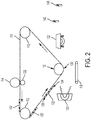
- exemplary three-dimensional (3-D) printers herein include, among other components, an intermediate transfer surface 110, such as a drum or intermediate transfer belt (ITB) supported on rollers 112, one or more printing components (e.g., development device 114).
- an intermediate transfer surface 110 such as a drum or intermediate transfer belt (ITB) supported on rollers 112
- one or more printing components e.g., development device 114.
- item 118 is a platen
- item 120 is a transfuse heater
- item 122 is a fusing station
- item 142 is a curing station (e.g., LED)
- item 148 is a support material removal station.
- item 130 is a transfuse nip
- items 134 and 136 denote the leading and trailing edges of each developed layer 102.
- Devices herein can include only one development device, as shown in Figure 2 , or can include many, as shown in Figure 20 , discussed below. Additionally, the platen 118 (which can be a surface or belt) is adjacent the ITB 110. In this example, the platen 118 is a vacuum belt.
- FIG 2 illustrates that the printing component 116 is positioned to electrostatically transfer material 102, such as a (potentially dry) powder polymer-wax material (e.g., charged 3-D toner) to the ITB 110.
- electrostatically transfer material 102 such as a (potentially dry) powder polymer-wax material (e.g., charged 3-D toner) to the ITB 110.
- the electrostatic transfer occurs by way of charge difference between the belt (produced by charge generator 128, for example) and the material being transferred 102.
- Element 102 is sometimes referred to as a "developed layer.”
- the developed layer 102 is on a discrete area of the ITB 110 and can be a uniform rectangle, or can be in a pattern corresponding to the components of the 3-D structure in that layer (and its associated support elements).
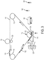
- the transfuse station 130 is adjacent the ITB 110.
- the transfuse station 130 includes a roller 112, on one side of the ITB 110, supporting the ITB 110.
- the transfuse station 130 is positioned to receive the layers 102 as the ITB 110 moves to the transfuse station 130. More specifically, the material development station 114 and the transfuse station 130 are positioned relative to the ITB 110 such that a layer 102 on the ITB 110, when the ITB 110 is moving in a process direction, first passes the material development station 114, and then passes the transfuse station 130.
- each of the developed layers 102 has a leading edge 134 oriented toward the processing direction in which the ITB 110 is moving (represented by arrows next to the ITB 110) and a trailing edge 136 opposite the leading edge 134.
- the platen 118 moves (using motors, gears, pulleys, cables, guides, etc. (all generally illustrated by item 118)) toward the ITB 110 to have the platen 118 make contact with the ITB 110.
- the developed layer 102 and ITB 110 are locally heated by heater 120 to bring the developed layer 102 to a "tacky" state prior to transfuse (i.e., to a temperature higher than the glass transition temperature (Tg) but short of the melt or fuse temperature Tm of the toner resin).
- the platen 118 is also heated by heater 120 to approximately the same temperature, and is then contacted synchronously with the tacky layer 102 as it translates through the ITB-platen nip (the transfuse nip 130). Thereby, the ITB 110 transfers one of the developed layers 102 of the build materials 102 and the support material 105 to the platen 118 each time the platen 118 contacts the ITB 110, to successively form developed layers 102 of the build material 102 and the support material 105 on the platen 118.
- the leading edge 134 of the developed layer 102 within the transfer nip 130 begins to be transferred to a corresponding location of the platen 118.
- the platen 118 moves to contact the developed layer 102 on the ITB 110 at a location where the leading edge 134 of the developed layer 102 is at the lowest location of the roller of the transfer nip 130.
- the trailing edge 136 of the developed layer 102 has not yet reached the transfer nip 130 and has not, therefore, yet been transferred to the platen 118.
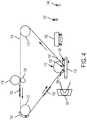
- the platen 118 moves synchronously with the ITB 110 (moves at the same speed and the same direction as the ITB 110) either by moving or rotating the platen vacuum belt, to allow the developed layers 102 to transfer cleanly to the platen 118, without smearing.
- the trailing edge 136 of the developed layer 102 is the only portion that has not yet reached the transfer nip 130 and has not, therefore, been transferred to the platen 118.
- the platen 118 moves at the same speed and in the same direction as the ITB 110, until the trailing edge 136 of the developed layer 102 reaches the bottom of the roller of the transfer nip 130, at which point the platen 118 moves away from the ITB 110 and over to the fusing station 142, as shown in Figure 5 .
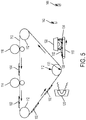
- the platen 118 moves to the fusing station 122, which can include a heated pressure roller 122.
- the platen 118 moves synchronously as the pressure roller rotates, heating and pressing the developed layer 102 to bond the developed layer 102 to the platen 118 (or to any previously transferred layers 102 existing on the platen 118).
- These synchronous movements between the platen 118 and the ITB 110 (and pressure roller) causes the pattern of support and build materials (102) that is printed by the development devices 114 and 116 to be transferred precisely from the ITB 110 to the platen 118, without distortion or smearing.
- the fusing station 122 is positioned between the transfuse station 130 and the curing station 142.
- the transfuse station 130, the fusing station 122, and the curing station 142 are positioned relative to the platen 118, such that the platen 118 first passes the transfuse station 130, then passes the fusing station 122, and then passes the curing station 142.
- the light emitting diode (LED) curing station 142 is positioned to selectively apply LED ultraviolet light to different portions of each layer 102 immediately after each layer is fused at the fusing station 122.
- the platen 118 moves to the curing station 142 after each time the ITB 110 transfers each of the developed layers 102 to the platen 118 (and after each of such layers are fused at the fusing station 122) to independently cure each of the developed layers 102 and successively join each developed layer 102 to the platen 118, to any previously transferred developed layers 102 already fused on the platen 118.
- the LED curing station 142 selectively applies the LED ultraviolet light 146 to the layer 102 to crosslink polymers together in portions of the layer 102 that are to be the build material. However, the LED curing station does not apply the LED ultraviolet light to a second portion of the layer that is to be the support material. Thus, the LED ultraviolet light crosslinks polymers in the portions of build material together, without crosslinking polymers in the support material, to leave the support material as an uncrosslinked material.
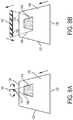
- Figures 8A-8B illustrates one of the layers 102 being processed at the curing station 142. More specifically, in Figure 8A , a single point source UV LED device 142 is able to directionally expose different areas of the uniform area of the layer of material 102, while in Figure 8B , the UV LED device 142 is an array device that also selectively exposes different areas. While two configurations are illustrated, those skilled in the art would understand that item 142 is any form of LED light that provides UV wavelength light in an addressable pattern to selectively illuminate certain portions (104) of the layer 102, without illuminating other portions (105).
- the single point LED 142 illustrated in Figure 8A provides a focused point of UV light (using lenses, prisms, etc. 143)), and the LED 142 includes motors, gears, etc. (all of which is schematically illustrated by item 142) to rotate (as shown by the arrows) to point the focused point of UV light at different locations on the layer 102 while the layer is stationary or moving, and thereby only provides UV radiation to selected portions of the layer 102.
- the single point LED 142 illustrated in Figure 8A provides a focused point of UV light (using lenses, prisms, etc. 143)), and the LED 142 includes motors, gears, etc. (all of which is schematically illustrated by item 142) to rotate (as shown by the arrows) to point the focused point of UV light at different locations on the layer 102 while the layer is stationary or moving, and thereby only provides UV radiation to selected portions of the layer 102.
- the LED 142 is illustrated as a full-width array of multiple LEDs 145.
- the array 142 can be at least as wide as the layer 102, the array 142 is an elongated structure that is positioned across (e.g. parallel to) the width of the layer, and the array 142 moves in a direction perpendicular to the width of the layer 102.
- the array of LEDs 142 moves relatively from the leading edge to the trailing edge of the layer 102 (as shown by the arrows) while selected ones of the LEDs 145 illuminate, and by this process the array of LEDs 142 only provides UV radiation to selected portions of the layer 102.
- the array of LEDs 142 can move using motors and gears (all of which is schematically illustrated by item 142) or the array of LEDs 142 can be stationary and the platen 118 containing the layer 102 can pass the layer 102 by the array of LEDs 142, as each individual LED 145 in the array 142 illuminates.
- Figures 8A and 8b illustrate but two ways in which the LED can be used to addressably provide UV radiation to selected portions (104) of the layer 102.
- LED ultraviolet light 146 cures a portion of material 102 to change it to build material 104 and does not provide LED ultraviolet light 146 to other portions of the layer 102 (and these non-cured portions are sometimes referred to as the "support material 105" to distinguish such from the cured build material 104, even though the support material is the same as the material of the layer 102).
- the LED ultraviolet light 146 crosslinks polymers in the exposed portions of material 104, without crosslinking polymers in the unexposed support material 105 to leave the support material 105 as an uncrosslinked fused material. Again, these portions of build material 104 and support material 105 are different portions of the same fused layer 102.
- materials 102 can be cured (without being fully melted) by heating such materials 102 to a temperature between their glass transition temperature and their melting temperature, to join the materials 102 as one, without affecting their shape or pattern, thereby creating a rigid structure.
- the platen moves to the curing station 142 before the layer 102 has cooled significantly, and while the layer 102 is still between the glass transition temperature and the melting temperature.
- the platen 118 can move to a cooling station that provides blown air (potentially cooled and dehumidified); or the platen 118 can pause to allow the layer 102 to cool before moving to the next processing step.
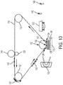
- the processing in Figures 2-7 is repeated to crosslink polymers in multiple developed layers 102 into a stack 106, as shown in Figure 9 .
- the fusing station 122 fuses together the material within each of the developed layers 102, and also fuses each developed player 102 to the immediately adjacent developed layer 102 that was most recently transferred to the platen 118 (e.g., joins layers 102 that contact one another on the platen 118).
- additional developed layers 102 are formed on top of the stack 106 ( Figure 10 ).
- such additional developed layers 102 are fused together by the fusing station 122.
- the curing station 142 selectively cures only portions of the very top layer to crosslink polymers in only the top layer 102 of the stack 106.
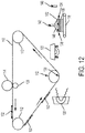
- Figure 13 shows the entire stack 106 is completely formed after all layers 102 have been transferred, fused, and cured.
- Figure 13 illustrates an overlay showing portions of support material 105 and build material 104 within the accumulation of the freestanding stack 106. Such may or may not be visible, and is only illustrated to show one exemplary way in which such build and support materials may be arranged.
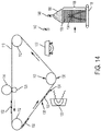
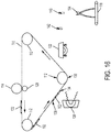
- the 3-D structure of the freestanding stack 106 can be output to allow manual removal of the support material 105 using an external solvent bath, etc; or automated processing can proceed as shown in Figure 14-16 . More specifically, as shown in Figure 14 , the support material removal station 148 is positioned to receive the now cured 3-D freestanding stack 106 on the platen 118. The support material removal station 148 applies a solvent, water, etc., 156. Any solvent 156 applied by the support material removal station 148 is selected to dissolve the support material 105 without affecting the build material 104. Again, as noted above, the solvent utilized will depend upon the chemical makeup of the build material 104 and the support material 105.
- Figure 15 illustrates the processing where about half of the support material 105 remains, and a portion of the build material 104 protrudes from the remaining stack of support material 105.
- Figure 16 illustrates processing after the support material removal station 148 has dissolved or removed all the support material 105, leaving only the build material 104 remaining, which leave a completed 3-D structure made of only the build material 104.
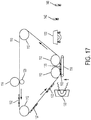
- FIGs 17 and 18 illustrate an alternative 3-D electrostatic printing structure herein which includes a planar transfuse station 138 in place of the transfer nip 130 shown in Figure 1 .
- the planar transfuse station 138 is a planar portion of the ITB 110 that is between rollers 112 and is parallel to the platen 118.
- FIG 18 with this structure, when the platen 118 moves to contact the planar transfuse station 138, all of the developed layer 102 is transferred simultaneously to the platen 118 or partially formed stack 106, avoiding the rolling transfer process shown in Figures 3 and 4 .
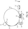
- a drum 158 could be used in place of the ITB 110, with all other components operating as described herein.
- the drum 158 could be an intermediate transfer surface receiving material from development station 114, as described above, or could be a photoreceptor and operate as the photoreceptor 256 described below operates, by maintaining a latent image of charge and receiving materials from development devices 254.
- FIG. 20 illustrates many components of 3-D printer structures 204 herein.
- the 3-D printing device 204 includes a controller/tangible processor 224 and a communications port (input/output) 214 operatively connected to the tangible processor 224 and to a computerized network external to the printing device 204.
- the printing device 204 can include at least one accessory functional component, such as a graphic user interface (GUI) assembly 212.
- GUI graphic user interface
- the input/output device 214 is used for communications to and from the 3-D printing device 204 and comprises a wired device or wireless device (of any form, whether currently known or developed in the future).
- the tangible processor 224 controls the various actions of the printing device 204.
- a non-transitory, tangible, computer storage medium device 210 (which can be optical, magnetic, capacitor based, etc., and is different from a transitory signal) is readable by the tangible processor 224 and stores instructions that the tangible processor 224 executes to allow the computerized device to perform its various functions, such as those described herein.
- a body housing has one or more functional components that operate on power supplied from an alternating current (AC) source 220 by the power supply 218.
- the power supply 218 can comprise a common power conversion unit, power storage element (e.g., a battery, etc), etc.
- the 3-D printing device 204 includes at least one marking device (printing engine(s)) 240 that deposits successive layers of build and support material on a platen as described above, and are operatively connected to a specialized image processor 224 (that is different than a general purpose computer because it is specialized for processing image data). Also, the printing device 204 can include at least one accessory functional component (such as a scanner 232) that also operates on the power supplied from the external power source 220 (through the power supply 218).
- a marking device printing engine(s)
- a specialized image processor 224 that is different than a general purpose computer because it is specialized for processing image data.
- the printing device 204 can include at least one accessory functional component (such as a scanner 232) that also operates on the power supplied from the external power source 220 (through the power supply 218).
- the one or more printing engines 240 are intended to illustrate any marking device that applies build and support materials (toner, etc.) whether currently known or developed in the future and can include, for example, devices that use an intermediate transfer belt 110 (as shown in Figure 21 ).
- each of the printing engine(s) 240 shown in Figure 20 can utilize one or more potentially different (e.g., different color, different material, etc.) build material development stations 152-158, one or more potentially different (e.g., different color, different material, etc.) support material development stations, etc.
- the development stations 152-158 can be any form of development station, whether currently known or developed in the future, such as individual electrostatic marking stations, individual inkjet stations, individual dry ink stations, etc.
- Each of the development stations 152-158 transfers a pattern of material to the same location of the intermediate transfer belt 110 in sequence during a single belt rotation (potentially independently of a condition of the intermediate transfer belt 110) thereby, reducing the number of passes the intermediate transfer belt 110 should make before a full and complete image is transferred to the intermediate transfer belt 110.
- Figure 21 illustrates different color development stations 152-158 positioned to electrostatically transfer different color materials to an intermediate transfer belt (ITB 110); for example, each different development station 152-158 can provide a color of material that is different from the colors of the materials supplied by other development stations 152-158. While Figure 21 illustrates four development stations adjacent or in contact with a rotating belt (110), as would be understood by those ordinarily skilled in the art, such devices could use any number of marking stations (e.g., 1, 2, 3, 5, 8, 11, etc.).
- Each of the individual electrostatic development stations 114 includes its own charging station 258 that creates a uniform charge on an internal photoreceptor 256, an internal exposure device 260 that patterns the uniform charge into a latent image of charge, and an internal development device 254 that transfers build or support material to the photoreceptor 256 in a pattern matching the charge latent image.
- the pattern of build or support material is then drawn from the photoreceptor 256 to the intermediate transfer belt 110 by way of an opposite charge of the intermediate transfer belt 110 relative to the charge of the build or support material, that is usually created by a charge generator 128 on the opposite side of the intermediate transfer belt 110.
- UV curable toner contains a resin with ethylenic unsaturation (double bonds) in the resin backbone structure, an optional crosslinking agent which bonds adjacent polymer strands together and a UV photoinitiator.
- the crosslinking agent is omitted as the polymer backbone of the toner resin contains ethylenic unsaturation can achieve the desired crosslinking with adjacent polymer backbones.
- various high temperature stable crosslinking agents can also be incorporated into the material toner resin 102, if desired
- an additive manufacturing system for printing a 3-D part using electrophotography includes a photoconductor component having a surface, and a development station, where the development station is configured to developed layers of a material on the surface of the photoconductor component.
- the system also includes a transfer medium configured to receive the developed layers from the surface of the rotatable photoconductor component, and a platen configured to receive the developed layers from the transfer component in a layer-by-layer manner to print the 3-D part from at least a portion of the received layers.
- UV curable toners As disclosed in US 7,250,238 it is known to provide a UV curable toner composition, as are methods of utilizing the UV curable toner compositions in printing processes.
- US 7,250,238 discloses various toner emulsion aggregation processes that permit the generation of toners that in embodiments can be cured, that is by the exposure to UV radiation, such as UV ultraviolet light of has about 100 nm to about 400 nm.
- the toner compositions produced can be utilized in various printing applications such as temperature sensitive packaging and the production of foil seals.
- a UV curable toner composition comprised of an optional colorant, an optional wax, a polymer generated from styrene, and acrylate selected from the group consisting of butyl acrylate, carboxyethyl acrylate, and a UV ultraviolet light curable acrylate oligomer. Additionally, these aspects relate to a toner composition comprised of a colorant such as a pigment, an optional wax, and a polymer generated from a UV curable cycloaliphatic epoxide.
- US 7,250,238 discloses a method of forming a UV curable toner composition
- a method of forming a UV curable toner composition comprising mixing a latex containing a polymer formed from styrene, butyl acrylate, a carboxymethyl acrylate, and a UV curable acrylate with a colorant and wax; adding flocculant to this mixture to optionally induce aggregation and form toner precursor particles dispersed in a second mixture; heating the toner precursor particles to a temperature equal to or higher than the glass transition temperature (Tg) of the polymer to form toner particles; optionally washing the toner particles; and optionally drying the toner particles.
- Tg glass transition temperature
- Computerized devices that include chip-based central processing units (CPU's), input/output devices (including graphic user interfaces (GUI), memories, comparators, tangible processors, etc.) are well-known and readily available devices produced by manufacturers such as Dell Computers, Round Rock TX, USA and Apple Computer Co., Cupertino CA, USA.
- Such computerized devices commonly include input/output devices, power supplies, tangible processors, electronic storage memories, wiring, etc., the details of which are omitted herefrom to allow the reader to focus on the salient aspects of the systems and methods described herein.
- printers, copiers, scanners and other similar peripheral equipment are available from Xerox Corporation, Norwalk, CT, USA and the details of such devices are not discussed herein for purposes of brevity and reader focus.
- printer or printing device encompasses any apparatus, such as a digital copier, bookmaking machine, facsimile machine, multifunction machine, etc., which performs a print outputting function for any purpose.
- the details of printers, printing engines, etc. are well-known and are not described in detail herein to keep this disclosure focused on the salient features presented.
- the systems and methods herein can encompass systems and methods that print in color, monochrome, or handle color or monochrome image data. All foregoing systems and methods are specifically applicable to electrostatographic and/or xerographic machines and/or processes.
- the term fixing means the drying, hardening, polymerization, crosslinking, binding, or addition reaction or other reaction of the coating.
- terms such as “right”, “left”, “vertical”, “horizontal”, “top”, “bottom”, “upper”, “lower”, “under”, “below”, “underlying”, “over”, “overlying”, “parallel”, “perpendicular”, etc., used herein are understood to be relative locations as they are oriented and illustrated in the drawings (unless otherwise indicated). Terms such as “touching”, “on”, “in direct contact”, “abutting”, “directly adjacent to”, etc., mean that at least one element physically contacts another element (without other elements separating the described elements).
- the terms automated or automatically mean that once a process is started (by a machine or a user), one or more machines perform the process without further input from any user.
- the same identification numeral identifies the same or similar item.
Description
- Systems and methods herein generally relate to three-dimensional (3-D) printing processes that use electrostatic printing processes.
- In general 3-D parts are built from a digital representation of the part that is divided into multiple horizontal slices. Instructions for printing individual layers are sent by a controller to the print process to form any given layer. Three-dimensional printing can produce objects using, for example, ink-jet printers.
- In one exemplary three-stage process, an ink jet device selectively deposits support and build material in a layer on a platen, and each layer is hardened using a UV ultraviolet light source to crosslink the polymers of the material. These steps are repeated layer-by-layer. Support materials generally comprise acid-, base- or watersoluble polymers, which can be selectively rinsed from the build material after 3-D printing is complete.
- The electrostatic (electro-photographic) process is a well-known means of generating two-dimensional digital images, which transfer materials onto an intermediate surface (such as a photoreceptor belt or drum). Advancements in the way an electro-photographic image is transferred can leverage the speed, efficiency and digital nature of printing systems.
-
CN-A-104890241 discloses three-dimensional rapid prototyping equipment and a prototyping method. The three-dimensional rapid prototyping equipment comprises a first development component, wherein the first development component comprises a first development agent; the first development agent is an UV photocuring development agent; a second development component comprises a second development agent; an annular transfer printing belt is used for bearing the first development agent and the second development agent; a charge generation device can enable the annular transfer printing belt to generate charges; a printing platform is used for bearing the first development agent and the second development agent on the annular transfer printing belt to form a thin layer; an UV photocuring light source is used for irradiating the thin layer to cure the first development agent; a heating device preheats the printing platform; and a heating and flattening device heats and flattens the thin layer. A support material is liable to be removed without damaging the surface of a prototyping structure of a three-dimensional object; the energy consumption can be reduced; the UV photocuring time is shortened; and the warpage and shrinkage effect caused by uneven heating of the development agent on the first thin layer is reduced. - The present invention relates to an apparatus according to claim 1 and to a method according to claim 7. Exemplary three-dimensional (3-D) printers include, among other components, an intermediate transfer surface, development stations positioned to electrostatically transfer different materials to the intermediate transfer surface, and a transfuse station adjacent the intermediate transfer surface. The transfuse station is positioned to receive layers of the different materials as the intermediate transfer surface moves past the transfuse station. The fusing station is positioned between the transfuse station and the curing station. The transfuse station, the fusing station, and the curing station are positioned relative to the platen, such that the platen first passes the transfuse station, then passes the fusing station, and then passes the curing station.
- Such structures also include a platen moving relative to the intermediate transfer surface. The intermediate transfer surface transfers a layer of the different materials to the platen each time the platen contacts one of the layers on the intermediate transfer surface at the transfuse station to successively form a freestanding stack of the layers on the platen. After being transfused to the platen or to the top of the existing freestanding stack on the platen, a fusing station applies heat and pressure to fuse the layers on the platen together.
- Additionally, a light emitting diode (LED) curing station is positioned to selectively apply LED ultraviolet light to different portions of each layer immediately after the layer is fused at the fusing station. The LED curing station selectively applies the LED ultraviolet light to the layer to crosslink polymers together in portions of the layer that are to be the build material. However, the LED curing station is adapted to not apply the LED ultraviolet light to a second portion of the layer that is to be the support material. Thus, the LED ultraviolet light crosslinks polymers in the portions of build material together, without crosslinking polymers in the support material to leave the support material as an uncrosslinked material. The portions of build material to which LED ultraviolet light is applied are less than all of the layer (thus, and these portions of build material and the support material are different portions within the layer).
- The 3-D printer can also optionally include a material removal station positioned to remove the support material of the different materials within the layer to separate the portions of build material of the different materials from the support material of the different materials and leave a 3-D printed part. For example, the material removal station can include a solvent rinsing device, etc.
- These and other features are described in, or are apparent from, the following detailed description.
- Various exemplary systems and methods are described in detail below, with reference to the attached drawing figures, in which:
-
Figure 1 is a chart showing a melt rheology curve; -
Figures 2-7 are schematic cross-section diagrams partially illustrating printing devices herein; -
Figures 8A-8B are perspective schematic diagrams illustrating LED curing herein; -
Figure 9 is an expanded schematic diagram illustrating stacks of layers formed by devices herein; -
Figures 10-19 are schematic cross-section diagrams partially illustrating printing devices herein; -
Figure 20 is a schematic diagram illustrating a 3-D printing device herein; -
Figure 21 is a schematic diagram illustrating a printing engine herein; and -
Figure 22 is an expanded schematic diagram illustrating a development device herein. - As mentioned above, electrostatic printing process are well-known processes for generating two-dimensional (2-D) digital images, and the methods and devices herein use such processing for the production of 3-D items (for 3-D printing). However, with 3-D printing that uses electrostatic processes, the mechanical integrity of the printed material may be compromised if it is very thin, and the transfer process can impose stripping shear forces that damage the material.
- In order to improve 3-D printing, this disclosure combines electrostatic printing with addressable LED curing. This involves using an electrostatic system to create layers of materials such as thermoplastics, ceramics, etc., and uses LEDs to cure the layers in order to create a 3-D part. The devices and methods herein take advantage of the fast image and material management process of electrostatic printing, and utilize a LED to crosslink polymers in the materials. 3-D processes are predicated on layer-by-layer transfuse of the build and support material, and the materials desirably have similar melt rheological properties and hence similar chemical structures; however, using materials having similar melt rheological properties makes separation by dissolution a difficult task.
- Many 3-D printing processes provide for co-deposition of different build and support materials, where the support material fills in the voids in the build materials in order to mechanically support the 3-D part being printed. One aspect of selection of support material in 3-D printers that use an intermediate transfer belt (ITB) is that the support material should have nearly the same melt rheology as the build material.
- The melt rheology requirements can be understood by considering the idealized melt rheology curve for a hypothetical toner resin as shown in
Figure 1 . In the initial heating of the developed layer on the ITB as well as the heating of the already formed layers on the platen to the tacky state, the toner resin should be heated slightly above the glass transition temperature (Tg) but should remain well below the melting temperature (Tm) so that the integrity of the layers on the platen is maintained during transfuse, and the integrity of the transferring layer is also maintained. During the post transfer fusing step a temperature closer to Tm should be imparted to the layers to fuse the uppermost layer to the layers below. So given a particular pre-transfuse temperature, it is desirable that both the support and build material be in a similar state of tackiness and that the melt points for both be similar as well. - This implies that the melt rheology curves for both build and support material should be rather similar, otherwise there may be a loss of latitude in the temperature set points and poor transfuse of one material or the other. This sets up strict limitations in the selection of support and build material, and therefore additional work is performed to tune the resin chemical structures (e.g. molecular weight, nature of functional groups) to achieve similar melt rheology curves for the two materials.
- In order to address such issues, the systems and methods here use the same material for both the support and build portions of the 3-D structure being printed; however, only the build portions are exposed to UV light and, therefore, only the polymers of the build portions are crosslinked, and the non-exposed portions (support portions) are not crosslinked. This allows the build portions to be rinsed from the support portions after printing is completed, to leave only the build portions as the completed 3-D printed part.
- Thus, one general approach to separating the support from the build material is by taking advantage of differences in solubility of the two materials. It is desirable to make the support material soluble in a solvent which will not dissolve the build material. Generally speaking the latter condition is at odds with the requirement that the melt rheologies be similar. Similar melt rheologies implies similar chemical structures (molecular weight, functional groups) while the solubility disparity implies different chemical structures (different molecular weights and functional groups). Again, the systems and methods described herein reconcile differing requirements for the build and support material, while improving the mechanical properties (strength, impact resistance, etc.) of the support material made from current toners and resins by using the same material for both the support and build portions of the 3-D structure being printed; however, only the build portions are exposed to UV light and, therefore, only the polymers of the build portions are crosslinked.
- Because of such issues, with methods and devices herein both the build and support materials start as a single, uniform UV radiation curable toner material. A UV LED image bar is used to image-wise expose the deposited toner after transfusing to the previously formed stack. The image-wise crosslinked toner thus becomes the build material. Rather than developing the build material pattern by having a development device transfer build material in a specific pattern to the ITB, with methods and devices herein the build pattern is created by selectively illuminating only portions of the uniform layer during post-process UV LED curing. Therefore, the unexposed areas of the uniform layer correspond to the support material. This avoids having the user find two materials that are mutually compatible with tacky transfer at the transfuse station, and provides substantial savings in both effort and cost. Additionally, using an LED to perform the UV exposure provides substantial cost and packaging benefits because LEDs are not only very power efficient, they are generally relatively inexpensive, and relatively small when compared to larger, more expensive devices such as lasers, etc.
- More specifically, the developed layer and ITB are locally heated to bring the developed layer to a "tacky" state prior to transfuse (i.e., to a temperature higher than the glass transition temperature (Tg) but short of the melt or fuse temperature Tm of the toner resin). A heated platen (heated to approximately the same temperature) is then contacted synchronously with the tacky layer as it translates through the ITB-platen nip. Thus, rather than being transferred electrostatically (based on toner/belt charge differences), it is the tacky nature of the developed layer and heated platen (or previously transferred developed layers) that causes the developed layer to transfer to the platen (or previously transferred developed layers). The platen is heated to keep the toner in a tacky state as it contacts the heated toner/ITB interface, and doing so allows the toner layer to separate from the ITB and transfer under pressure to the platen surface which may contain previously deposited layers. Wax (which is present in many toners) can be included in the build/support material formulation to assist the tacky toner layer in departing from the ITB. Thus a waxy toner can be used to help parting the developed/heated layer from the ITB. Alternatively an ITB with a "Teflon-like" coating can be employed.
- Following transfuse to the platen, additional heat is applied to the built up layers on the platen to fuse the top layer to those beneath it. The temperature at this step should be nearer to the melting temperature of the toner resin. At this temperature there is sufficient mobility of the individual polymer backbone chains to physically approach each other. While the toner resin is in this more liquid like state, UV radiation is selectively applied to the portions of the layer where the part being built up is located. Because only those areas which are UV exposed will be crosslinked, these areas will correspond to the build material, leaving the unexposed uncrosslinked areas functioning as the support material.
- Following this, the part material is cooled to nearer the Tg and the platen is returned to its home position ready to add an additional layer. Repetition of this process allows the build of thicker layers from which a part may be fabricated.
- An additional consideration with UV illumination is that any support layers beneath the UV exposed build layers should not be inadvertently exposed and crosslinked. This can be controlled by judicious selection of the nature and concentration of photoinitiator within the build/support material. In one example, the photoinitiator may be controlled to be present in the build/support material resin at a loading of 1-5 wt%. With some materials only 1% of the light will penetrate 40 µm into such a layer. This may be an acceptable penetration depth for the UV radiation of layers having thickness greater than 40 µm. In other examples the photoinitiator loading can be increased or decreased so that the UV penetration can be controlled to correspond to the thickness of the layers being printed. Thus, while specific photoinitiator concentrations and thicknesses are mentioned herein, such are only examples, and those ordinarily skilled in the art would understand that any concentrations of photoinitiator can be used, so long as the UV exposure does not have significant inadvertent penetration to the lower layers that have been previously UV cured.
- The devices and methods herein can use a single development station, or a series of development stations, one for each different color or different material. For example, multiple development stations could be used, with the only material difference of the toner being color (and all other material characteristics being the same). Alternatively, different development stations could provide different materials.
- However, if a single development station is used, a continuous uniform layer of the same material is electrostatically transferred to the ITB. If multiple development stations are used, each of the stations develops and transfers a different image to the ITB electrostatically. The multiple material images are combined into a single developed layer on the ITB.
- The developed layer is then heated to become tacky, and is transferred to a platen. Once the developed layer has been transferred into the platen, the platen moves to the LED curing station. The curing station selectively cures only portions of the material particles in order to create a solid part. Once the curing is performed, the platen moves to the home (initial) position to repeat the process and add the next layer. This process repeats until a solid part is created. Thus, the devices and methods herein are able to create parts or assemblies (potentially with multiple materials and/or colors). This takes advantage of fast electrostatic printing processes to create 3-D items faster.
- As shown in
Figure 2 , exemplary three-dimensional (3-D) printers herein include, among other components, anintermediate transfer surface 110, such as a drum or intermediate transfer belt (ITB) supported onrollers 112, one or more printing components (e.g., development device 114). InFigure 2 ,item 118 is a platen,item 120 is a transfuse heater,item 122 is a fusing station,item 142 is a curing station (e.g., LED), anditem 148 is a support material removal station. Additionally,item 130 is a transfuse nip, anditems developed layer 102. Devices herein can include only one development device, as shown inFigure 2 , or can include many, as shown inFigure 20 , discussed below. Additionally, the platen 118 (which can be a surface or belt) is adjacent theITB 110. In this example, theplaten 118 is a vacuum belt. -
Figure 2 illustrates that theprinting component 116 is positioned to electrostaticallytransfer material 102, such as a (potentially dry) powder polymer-wax material (e.g., charged 3-D toner) to theITB 110. The electrostatic transfer occurs by way of charge difference between the belt (produced bycharge generator 128, for example) and the material being transferred 102.Element 102 is sometimes referred to as a "developed layer." Thedeveloped layer 102 is on a discrete area of theITB 110 and can be a uniform rectangle, or can be in a pattern corresponding to the components of the 3-D structure in that layer (and its associated support elements). - As shown in
Figure 3 , thetransfuse station 130 is adjacent theITB 110. Thetransfuse station 130 includes aroller 112, on one side of theITB 110, supporting theITB 110. Thetransfuse station 130 is positioned to receive thelayers 102 as theITB 110 moves to thetransfuse station 130. More specifically, thematerial development station 114 and thetransfuse station 130 are positioned relative to theITB 110 such that alayer 102 on theITB 110, when theITB 110 is moving in a process direction, first passes thematerial development station 114, and then passes thetransfuse station 130. - Therefore, the material that is printed in on the ITB by
development device 114 forms thedeveloped layers 102 having a predetermined length. Again, as shown inFigure 3 , each of thedeveloped layers 102 has aleading edge 134 oriented toward the processing direction in which theITB 110 is moving (represented by arrows next to the ITB 110) and a trailingedge 136 opposite theleading edge 134. - As shown by the vertical arrow in
Figure 3 , theplaten 118 moves (using motors, gears, pulleys, cables, guides, etc. (all generally illustrated by item 118)) toward theITB 110 to have theplaten 118 make contact with theITB 110. Thedeveloped layer 102 andITB 110 are locally heated byheater 120 to bring thedeveloped layer 102 to a "tacky" state prior to transfuse (i.e., to a temperature higher than the glass transition temperature (Tg) but short of the melt or fuse temperature Tm of the toner resin). Theplaten 118 is also heated byheater 120 to approximately the same temperature, and is then contacted synchronously with thetacky layer 102 as it translates through the ITB-platen nip (the transfuse nip 130). Thereby, theITB 110 transfers one of thedeveloped layers 102 of thebuild materials 102 and thesupport material 105 to theplaten 118 each time theplaten 118 contacts theITB 110, to successively formdeveloped layers 102 of thebuild material 102 and thesupport material 105 on theplaten 118. - More specifically, as shown in
Figure 3 , at the transfer nip 130, theleading edge 134 of the developedlayer 102 within the transfer nip 130 begins to be transferred to a corresponding location of theplaten 118. Thus, theplaten 118 moves to contact thedeveloped layer 102 on theITB 110 at a location where theleading edge 134 of the developedlayer 102 is at the lowest location of the roller of the transfer nip 130. In this example, the trailingedge 136 of the developedlayer 102 has not yet reached the transfer nip 130 and has not, therefore, yet been transferred to theplaten 118. - As shown in
Figure 4 , theplaten 118 moves synchronously with the ITB 110 (moves at the same speed and the same direction as the ITB 110) either by moving or rotating the platen vacuum belt, to allow thedeveloped layers 102 to transfer cleanly to theplaten 118, without smearing. InFigure 4 , the trailingedge 136 of the developedlayer 102 is the only portion that has not yet reached the transfer nip 130 and has not, therefore, been transferred to theplaten 118. Then, as theITB 110 moves in the processing direction, theplaten 118 moves at the same speed and in the same direction as theITB 110, until the trailingedge 136 of the developedlayer 102 reaches the bottom of the roller of the transfer nip 130, at which point theplaten 118 moves away from theITB 110 and over to the fusingstation 142, as shown inFigure 5 . - In
Figure 5 , theplaten 118 moves to the fusingstation 122, which can include aheated pressure roller 122. As shown inFigure 6 , theplaten 118 moves synchronously as the pressure roller rotates, heating and pressing thedeveloped layer 102 to bond thedeveloped layer 102 to the platen 118 (or to any previously transferredlayers 102 existing on the platen 118). These synchronous movements between theplaten 118 and the ITB 110 (and pressure roller) causes the pattern of support and build materials (102) that is printed by thedevelopment devices ITB 110 to theplaten 118, without distortion or smearing. - As shown in
Figure 7 , the fusingstation 122 is positioned between thetransfuse station 130 and the curingstation 142. Thetransfuse station 130, the fusingstation 122, and the curingstation 142 are positioned relative to theplaten 118, such that theplaten 118 first passes thetransfuse station 130, then passes the fusingstation 122, and then passes the curingstation 142. Thus, the light emitting diode (LED) curingstation 142 is positioned to selectively apply LED ultraviolet light to different portions of eachlayer 102 immediately after each layer is fused at the fusingstation 122. Theplaten 118 moves to the curingstation 142 after each time theITB 110 transfers each of thedeveloped layers 102 to the platen 118 (and after each of such layers are fused at the fusing station 122) to independently cure each of thedeveloped layers 102 and successively join eachdeveloped layer 102 to theplaten 118, to any previously transferred developedlayers 102 already fused on theplaten 118. - The
LED curing station 142 selectively applies theLED ultraviolet light 146 to thelayer 102 to crosslink polymers together in portions of thelayer 102 that are to be the build material. However, the LED curing station does not apply the LED ultraviolet light to a second portion of the layer that is to be the support material. Thus, the LED ultraviolet light crosslinks polymers in the portions of build material together, without crosslinking polymers in the support material, to leave the support material as an uncrosslinked material. -
Figures 8A-8B illustrates one of thelayers 102 being processed at the curingstation 142. More specifically, inFigure 8A , a single point sourceUV LED device 142 is able to directionally expose different areas of the uniform area of the layer ofmaterial 102, while inFigure 8B , theUV LED device 142 is an array device that also selectively exposes different areas. While two configurations are illustrated, those skilled in the art would understand thatitem 142 is any form of LED light that provides UV wavelength light in an addressable pattern to selectively illuminate certain portions (104) of thelayer 102, without illuminating other portions (105). - For example, the
single point LED 142 illustrated inFigure 8A provides a focused point of UV light (using lenses, prisms, etc. 143)), and theLED 142 includes motors, gears, etc. (all of which is schematically illustrated by item 142) to rotate (as shown by the arrows) to point the focused point of UV light at different locations on thelayer 102 while the layer is stationary or moving, and thereby only provides UV radiation to selected portions of thelayer 102. - In another example shown in
Figure 8B , theLED 142 is illustrated as a full-width array ofmultiple LEDs 145. Thearray 142 can be at least as wide as thelayer 102, thearray 142 is an elongated structure that is positioned across (e.g. parallel to) the width of the layer, and thearray 142 moves in a direction perpendicular to the width of thelayer 102. Thus, the array ofLEDs 142 moves relatively from the leading edge to the trailing edge of the layer 102 (as shown by the arrows) while selected ones of theLEDs 145 illuminate, and by this process the array ofLEDs 142 only provides UV radiation to selected portions of thelayer 102. The array ofLEDs 142 can move using motors and gears (all of which is schematically illustrated by item 142) or the array ofLEDs 142 can be stationary and theplaten 118 containing thelayer 102 can pass thelayer 102 by the array ofLEDs 142, as eachindividual LED 145 in thearray 142 illuminates. Those ordinarily skilled in the art would understand thatFigures 8A and 8b illustrate but two ways in which the LED can be used to addressably provide UV radiation to selected portions (104) of thelayer 102. - Therefore, in both
Figures 8A and 8B ,LED ultraviolet light 146 cures a portion ofmaterial 102 to change it to buildmaterial 104 and does not provideLED ultraviolet light 146 to other portions of the layer 102 (and these non-cured portions are sometimes referred to as the "support material 105" to distinguish such from the curedbuild material 104, even though the support material is the same as the material of the layer 102). Thus, theLED ultraviolet light 146 crosslinks polymers in the exposed portions ofmaterial 104, without crosslinking polymers in theunexposed support material 105 to leave thesupport material 105 as an uncrosslinked fused material. Again, these portions ofbuild material 104 andsupport material 105 are different portions of the same fusedlayer 102. - Regarding the curing process,
materials 102 can be cured (without being fully melted) by heatingsuch materials 102 to a temperature between their glass transition temperature and their melting temperature, to join thematerials 102 as one, without affecting their shape or pattern, thereby creating a rigid structure. Thus, with methods and devices herein, the platen moves to the curingstation 142 before thelayer 102 has cooled significantly, and while thelayer 102 is still between the glass transition temperature and the melting temperature. - Those ordinarily skilled in the art would understand that the selection of build and support materials is coordinated with the type of curing process performed by the curing
station 142. Further, other curing processing and components could be used, and that the foregoing is presented only as one limited example; and the devices and methods herein are applicable to all such methods and components, whether currently known or developed in the future. Further, in such processing theplaten 118 can move to a cooling station that provides blown air (potentially cooled and dehumidified); or theplaten 118 can pause to allow thelayer 102 to cool before moving to the next processing step. - The processing in
Figures 2-7 is repeated to crosslink polymers in multipledeveloped layers 102 into astack 106, as shown inFigure 9 . The fusingstation 122 fuses together the material within each of thedeveloped layers 102, and also fuses eachdeveloped player 102 to the immediately adjacentdeveloped layer 102 that was most recently transferred to the platen 118 (e.g., joinslayers 102 that contact one another on the platen 118). As thestack 106 of thedeveloped layers 102 grows, additionaldeveloped layers 102 are formed on top of the stack 106 (Figure 10 ). As shown inFigure 11 , such additionaldeveloped layers 102 are fused together by the fusingstation 122. InFigure 12 , the curingstation 142 selectively cures only portions of the very top layer to crosslink polymers in only thetop layer 102 of thestack 106. -
Figure 13 shows theentire stack 106 is completely formed after alllayers 102 have been transferred, fused, and cured. In addition,Figure 13 illustrates an overlay showing portions ofsupport material 105 and buildmaterial 104 within the accumulation of thefreestanding stack 106. Such may or may not be visible, and is only illustrated to show one exemplary way in which such build and support materials may be arranged. - The 3-D structure of the
freestanding stack 106 can be output to allow manual removal of thesupport material 105 using an external solvent bath, etc; or automated processing can proceed as shown inFigure 14-16 . More specifically, as shown inFigure 14 , the supportmaterial removal station 148 is positioned to receive the now cured 3-Dfreestanding stack 106 on theplaten 118. The supportmaterial removal station 148 applies a solvent, water, etc., 156. Any solvent 156 applied by the supportmaterial removal station 148 is selected to dissolve thesupport material 105 without affecting thebuild material 104. Again, as noted above, the solvent utilized will depend upon the chemical makeup of thebuild material 104 and thesupport material 105.Figure 15 illustrates the processing where about half of thesupport material 105 remains, and a portion of thebuild material 104 protrudes from the remaining stack ofsupport material 105.Figure 16 illustrates processing after the supportmaterial removal station 148 has dissolved or removed all thesupport material 105, leaving only thebuild material 104 remaining, which leave a completed 3-D structure made of only thebuild material 104. -
Figures 17 and18 illustrate an alternative 3-D electrostatic printing structure herein which includes aplanar transfuse station 138 in place of the transfer nip 130 shown inFigure 1 . As shown inFigure 17 , theplanar transfuse station 138 is a planar portion of theITB 110 that is betweenrollers 112 and is parallel to theplaten 118. As shown inFigure 18 , with this structure, when theplaten 118 moves to contact theplanar transfuse station 138, all of the developedlayer 102 is transferred simultaneously to theplaten 118 or partially formedstack 106, avoiding the rolling transfer process shown inFigures 3 and4 . Alternatively, as shown inFigure 19 , adrum 158 could be used in place of theITB 110, with all other components operating as described herein. Thus, thedrum 158 could be an intermediate transfer surface receiving material fromdevelopment station 114, as described above, or could be a photoreceptor and operate as thephotoreceptor 256 described below operates, by maintaining a latent image of charge and receiving materials fromdevelopment devices 254. -
Figure 20 illustrates many components of 3-D printer structures 204 herein. The 3-D printing device 204 includes a controller/tangible processor 224 and a communications port (input/output) 214 operatively connected to thetangible processor 224 and to a computerized network external to theprinting device 204. Also, theprinting device 204 can include at least one accessory functional component, such as a graphic user interface (GUI)assembly 212. The user may receive messages, instructions, and menu options from, and enter instructions through, the graphical user interface orcontrol panel 212. - The input/
output device 214 is used for communications to and from the 3-D printing device 204 and comprises a wired device or wireless device (of any form, whether currently known or developed in the future). Thetangible processor 224 controls the various actions of theprinting device 204. A non-transitory, tangible, computer storage medium device 210 (which can be optical, magnetic, capacitor based, etc., and is different from a transitory signal) is readable by thetangible processor 224 and stores instructions that thetangible processor 224 executes to allow the computerized device to perform its various functions, such as those described herein. Thus, as shown inFigure 20 , a body housing has one or more functional components that operate on power supplied from an alternating current (AC)source 220 by thepower supply 218. Thepower supply 218 can comprise a common power conversion unit, power storage element (e.g., a battery, etc), etc. - The 3-
D printing device 204 includes at least one marking device (printing engine(s)) 240 that deposits successive layers of build and support material on a platen as described above, and are operatively connected to a specialized image processor 224 (that is different than a general purpose computer because it is specialized for processing image data). Also, theprinting device 204 can include at least one accessory functional component (such as a scanner 232) that also operates on the power supplied from the external power source 220 (through the power supply 218). - The one or
more printing engines 240 are intended to illustrate any marking device that applies build and support materials (toner, etc.) whether currently known or developed in the future and can include, for example, devices that use an intermediate transfer belt 110 (as shown inFigure 21 ). - Thus, as shown in
Figure 21 , each of the printing engine(s) 240 shown inFigure 20 can utilize one or more potentially different (e.g., different color, different material, etc.) build material development stations 152-158, one or more potentially different (e.g., different color, different material, etc.) support material development stations, etc. The development stations 152-158 can be any form of development station, whether currently known or developed in the future, such as individual electrostatic marking stations, individual inkjet stations, individual dry ink stations, etc. Each of the development stations 152-158 transfers a pattern of material to the same location of theintermediate transfer belt 110 in sequence during a single belt rotation (potentially independently of a condition of the intermediate transfer belt 110) thereby, reducing the number of passes theintermediate transfer belt 110 should make before a full and complete image is transferred to theintermediate transfer belt 110. - Thus,
Figure 21 illustrates different color development stations 152-158 positioned to electrostatically transfer different color materials to an intermediate transfer belt (ITB 110); for example, each different development station 152-158 can provide a color of material that is different from the colors of the materials supplied by other development stations 152-158. WhileFigure 21 illustrates four development stations adjacent or in contact with a rotating belt (110), as would be understood by those ordinarily skilled in the art, such devices could use any number of marking stations (e.g., 1, 2, 3, 5, 8, 11, etc.). - One exemplary individual
electrostatic development station 114 is shown inFigure 22 positioned adjacent to (or potentially in contact with)intermediate transfer belt 110. Each of the individualelectrostatic development stations 114 includes itsown charging station 258 that creates a uniform charge on aninternal photoreceptor 256, aninternal exposure device 260 that patterns the uniform charge into a latent image of charge, and aninternal development device 254 that transfers build or support material to thephotoreceptor 256 in a pattern matching the charge latent image. The pattern of build or support material is then drawn from thephotoreceptor 256 to theintermediate transfer belt 110 by way of an opposite charge of theintermediate transfer belt 110 relative to the charge of the build or support material, that is usually created by acharge generator 128 on the opposite side of theintermediate transfer belt 110. - UV curable toner contains a resin with ethylenic unsaturation (double bonds) in the resin backbone structure, an optional crosslinking agent which bonds adjacent polymer strands together and a UV photoinitiator. Sometimes, the crosslinking agent is omitted as the polymer backbone of the toner resin contains ethylenic unsaturation can achieve the desired crosslinking with adjacent polymer backbones. Notwithstanding this, various high temperature stable crosslinking agents can also be incorporated into the
material toner resin 102, if desired - As shown in
US 8,488,994 , an additive manufacturing system for printing a 3-D part using electrophotography is known. The system includes a photoconductor component having a surface, and a development station, where the development station is configured to developed layers of a material on the surface of the photoconductor component. The system also includes a transfer medium configured to receive the developed layers from the surface of the rotatable photoconductor component, and a platen configured to receive the developed layers from the transfer component in a layer-by-layer manner to print the 3-D part from at least a portion of the received layers. - With respect to UV curable toners, as disclosed in
US 7,250,238 it is known to provide a UV curable toner composition, as are methods of utilizing the UV curable toner compositions in printing processes.US 7,250,238 discloses various toner emulsion aggregation processes that permit the generation of toners that in embodiments can be cured, that is by the exposure to UV radiation, such as UV ultraviolet light of has about 100 nm to about 400 nm. InUS 7,250,238 , the toner compositions produced can be utilized in various printing applications such as temperature sensitive packaging and the production of foil seals. InUS 7,250,238 embodiments relate to a UV curable toner composition comprised of an optional colorant, an optional wax, a polymer generated from styrene, and acrylate selected from the group consisting of butyl acrylate, carboxyethyl acrylate, and a UV ultraviolet light curable acrylate oligomer. Additionally, these aspects relate to a toner composition comprised of a colorant such as a pigment, an optional wax, and a polymer generated from a UV curable cycloaliphatic epoxide. - Moreover,
US 7,250,238 discloses a method of forming a UV curable toner composition comprising mixing a latex containing a polymer formed from styrene, butyl acrylate, a carboxymethyl acrylate, and a UV curable acrylate with a colorant and wax; adding flocculant to this mixture to optionally induce aggregation and form toner precursor particles dispersed in a second mixture; heating the toner precursor particles to a temperature equal to or higher than the glass transition temperature (Tg) of the polymer to form toner particles; optionally washing the toner particles; and optionally drying the toner particles. A further aspect relates to the toner particles produced by this method. - While some exemplary structures are illustrated in the attached drawings, those ordinarily skilled in the art would understand that the drawings are simplified schematic illustrations and that the claims presented below encompass many more features that are not illustrated (or potentially many less) but that are commonly utilized with such devices and systems. Therefore, Applicants do not intend for the claims presented below to be limited by the attached drawings, but instead the attached drawings are merely provided to illustrate a few ways in which the claimed features can be implemented.
- Many computerized devices are discussed above. Computerized devices that include chip-based central processing units (CPU's), input/output devices (including graphic user interfaces (GUI), memories, comparators, tangible processors, etc.) are well-known and readily available devices produced by manufacturers such as Dell Computers, Round Rock TX, USA and Apple Computer Co., Cupertino CA, USA. Such computerized devices commonly include input/output devices, power supplies, tangible processors, electronic storage memories, wiring, etc., the details of which are omitted herefrom to allow the reader to focus on the salient aspects of the systems and methods described herein. Similarly, printers, copiers, scanners and other similar peripheral equipment are available from Xerox Corporation, Norwalk, CT, USA and the details of such devices are not discussed herein for purposes of brevity and reader focus.
- The terms printer or printing device as used herein encompasses any apparatus, such as a digital copier, bookmaking machine, facsimile machine, multifunction machine, etc., which performs a print outputting function for any purpose. The details of printers, printing engines, etc., are well-known and are not described in detail herein to keep this disclosure focused on the salient features presented. The systems and methods herein can encompass systems and methods that print in color, monochrome, or handle color or monochrome image data. All foregoing systems and methods are specifically applicable to electrostatographic and/or xerographic machines and/or processes.
- For the purposes of this invention, the term fixing means the drying, hardening, polymerization, crosslinking, binding, or addition reaction or other reaction of the coating. In addition, terms such as "right", "left", "vertical", "horizontal", "top", "bottom", "upper", "lower", "under", "below", "underlying", "over", "overlying", "parallel", "perpendicular", etc., used herein are understood to be relative locations as they are oriented and illustrated in the drawings (unless otherwise indicated). Terms such as "touching", "on", "in direct contact", "abutting", "directly adjacent to", etc., mean that at least one element physically contacts another element (without other elements separating the described elements). Further, the terms automated or automatically mean that once a process is started (by a machine or a user), one or more machines perform the process without further input from any user. In the drawings herein, the same identification numeral identifies the same or similar item.
- It will be appreciated that the above-disclosed and other features and functions, or alternatives thereof, may be desirably combined into many other different systems or applications. Various presently unforeseen or unanticipated alternatives, modifications, variations, or improvements therein may be subsequently made by those skilled in the art which are also intended to be encompassed by the following claims. Unless specifically defined in a specific claim itself, steps or components of the systems and methods herein cannot be implied or imported from any above example as limitations to any particular order, number, position, size, shape, angle, color, or material.
Claims (9)
- A three-dimensional, 3-D, printer comprising:an intermediate transfer surface (110);a development station (114) positioned to electrostatically transfer layers (102) of material to said intermediate transfer surface (110);a transfuse station (130) adjacent said intermediate transfer surface (110);a platen (118) moving relative to said intermediate transfer surface (110), said intermediate transfer surface (110) transfers a layer (102) of said material to said platen (118) each time said platen (118) contacts one of said layers (102) on said intermediate transfer surface (110) at said transfuse station (130) to successively form a freestanding stack (106) of said layers (102) on said platen (118); anda curing station (142) positioned to apply ultraviolet light to said layer (102) after said layer (102) is transferred from said transfuse station (130) to said platen (118), characterized in that said curing station (142) is controlled to selectively apply said ultraviolet light to crosslink polymers in only a portion (104) of said material within said layer (102) where the part being built up is located.
- The 3-D printer according to claim 1, said curing station (142) is adapted to not apply said ultraviolet light to a second portion (105) of said material within said layer (102), and said ultraviolet light crosslinks polymers in said portion (104) together, without crosslinking polymers in said second portion (105), to leave said second portion (105) as an uncrosslinked material.
- The 3-D printer according to claim 1, said curing station is adapted to not apply said ultraviolet light to a second portion (105) of said material within said layer (102), said portion (104) is less than all of said layer (102), and said portion (104) and said second portion (105) are different portions of said layer (102).
- The 3-D printer according to claim 1, said curing station (142) is adapted to not apply said ultraviolet light to a second portion (105) of said material within said layer (102), and
said 3-D printer further comprises a material removal station (148) positioned to remove said second portion (105) to separate said portion (104) from said second portion (105), and leave a 3-D printed part. - The 3-D printer of any of claims 1-4, wherein the curing station (142) comprises a light emitting diode that provides UV wavelength light.
- The 3-D printer of any of claims 1-5, further comprising at least one additional development station (152, 154, 156, 158), wherein each of the development station (114) and the at least one additional development stations (152, 154, 156, 158) is positioned to electrostatically transfer a different color or material to the intermediate transfer surface (110).
- A method for three-dimensional, 3-D, printing using the 3-D printer of claim 1, the method comprising:causing the development station (114) to electrostatically transfer layers (102) of material to the intermediate transfer surface (110);causing the platen (118) to move relative to said intermediate transfer surface (110) adjacent to said platen, said intermediate transfer surface (110) transferring a layer (102) of said material to said platen (118) each time said platen (118) contacts one of said layers (102) on said intermediate transfer surface (110) at said transfuse station (130) to successively form a freestanding stack (106) of said layers (102) on said platen (118); andcausing the curing station (142) to apply ultraviolet light to said layer (102) after said layer (102) is transferred from said transfuse station (130) to said platen (118), characterized in that said curing station (142) is controlled to selectively apply said ultraviolet light to crosslink polymers in only a portion (104) of said material within said layer (102) where the part being built up is located.
- The method for three-dimensional (3-D) printing according to claim 7, wherein said curing station (142) is caused to not apply said ultraviolet light to a second portion (105) of said material within said layer (102), and said ultraviolet light crosslinks polymers in said portion (104) together, without crosslinking polymers in said second portion (105), to leave said second portion (105) as an uncrosslinked material.
- The method for three-dimensional (3-D) printing according to claim 7, wherein said curing station is caused to not apply said ultraviolet light to a second portion (105) of said material within said layer (102), said portion (104) is less than all of said layer (102), and said portion (104) and said second portion (105) are different portions of said layer (102).
Applications Claiming Priority (1)
| Application Number | Priority Date | Filing Date | Title |
|---|---|---|---|
| US15/152,651 US10005227B2 (en) | 2016-05-12 | 2016-05-12 | Electrostatic 3-D printer using addressable UV crosslinking |
Publications (2)
| Publication Number | Publication Date |
|---|---|
| EP3243657A1 EP3243657A1 (en) | 2017-11-15 |
| EP3243657B1 true EP3243657B1 (en) | 2019-01-09 |
Family
ID=58671483
Family Applications (1)
| Application Number | Title | Priority Date | Filing Date |
|---|---|---|---|
| EP17169601.6A Active EP3243657B1 (en) | 2016-05-12 | 2017-05-04 | Electrostatic 3-d printer using addressable uv crosslinking |
Country Status (5)
| Country | Link |
|---|---|
| US (1) | US10005227B2 (en) |
| EP (1) | EP3243657B1 (en) |
| JP (1) | JP6785183B2 (en) |
| KR (1) | KR102142833B1 (en) |
| CN (1) | CN107364123B (en) |
Families Citing this family (2)
| Publication number | Priority date | Publication date | Assignee | Title |
|---|---|---|---|---|
| US11426818B2 (en) | 2018-08-10 | 2022-08-30 | The Research Foundation for the State University | Additive manufacturing processes and additively manufactured products |
| US11534959B2 (en) * | 2020-09-24 | 2022-12-27 | Inkbit, LLC | Delayed cure additive manufacturing |
Family Cites Families (26)
| Publication number | Priority date | Publication date | Assignee | Title |
|---|---|---|---|---|
| US7250238B2 (en) | 2003-12-23 | 2007-07-31 | Xerox Corporation | Toners and processes thereof |
| US7184698B2 (en) | 2004-03-17 | 2007-02-27 | Eastman Kodak Company | Durable electrophotographic prints |
| US7690782B2 (en) | 2004-12-07 | 2010-04-06 | Xerox Corporation | Apparatus and process for printing ultraviolet curable inks |
| US7270408B2 (en) | 2005-01-14 | 2007-09-18 | Xerox Corporation | Low level cure transfuse assist for printing with radiation curable ink |
| US7851549B2 (en) | 2007-12-13 | 2010-12-14 | Xerox Corporation | Curable polyester latex made by phase inversion emulsification |
| US8876513B2 (en) * | 2008-04-25 | 2014-11-04 | 3D Systems, Inc. | Selective deposition modeling using CW UV LED curing |
| US8470231B1 (en) | 2009-06-01 | 2013-06-25 | Stratasys Ltd. | Three-dimensional printing process for producing a self-destructible temporary structure |
| JP2011020842A (en) * | 2009-07-21 | 2011-02-03 | Fuji Xerox Co Ltd | Sheet length measuring device and image forming device |
| JP2011028055A (en) * | 2009-07-27 | 2011-02-10 | Fuji Xerox Co Ltd | Image forming method, process cartridge and image forming apparatus |
| WO2013044047A1 (en) * | 2011-09-23 | 2013-03-28 | Stratasys, Inc. | Layer transfusion for additive manufacturing |
| US8488994B2 (en) | 2011-09-23 | 2013-07-16 | Stratasys, Inc. | Electrophotography-based additive manufacturing system with transfer-medium service loops |
| US8459280B2 (en) * | 2011-09-23 | 2013-06-11 | Stratasys, Inc. | Support structure removal system |
| US20130186558A1 (en) * | 2011-09-23 | 2013-07-25 | Stratasys, Inc. | Layer transfusion with heat capacitor belt for additive manufacturing |
| WO2014072147A1 (en) | 2012-11-09 | 2014-05-15 | Evonik Industries Ag | Multicoloured extrusion-based 3d printing |
| CN108381909B (en) | 2012-11-09 | 2021-05-25 | 赢创运营有限公司 | Use and preparation of coated filaments for extrusion 3D printing processes |
| EP2969489B1 (en) | 2013-03-12 | 2019-04-24 | Orange Maker Llc | 3d printing using spiral buildup |
| JP6376831B2 (en) * | 2013-06-20 | 2018-08-22 | キヤノン株式会社 | Manufacturing method of structure |
| US9144940B2 (en) * | 2013-07-17 | 2015-09-29 | Stratasys, Inc. | Method for printing 3D parts and support structures with electrophotography-based additive manufacturing |
| US9029058B2 (en) | 2013-07-17 | 2015-05-12 | Stratasys, Inc. | Soluble support material for electrophotography-based additive manufacturing |
| SG10201804040VA (en) | 2013-11-14 | 2018-07-30 | Structo Pte Ltd | Additive manufacturing device and method |
| US10369743B2 (en) | 2013-11-18 | 2019-08-06 | San Draw Inc. | Color or multi-material three-dimensional (3D) printing |
| US9744730B2 (en) | 2013-11-22 | 2017-08-29 | Stratasys, Inc. | Magnetic platen assembly for additive manufacturing system |
| EP3083197A1 (en) * | 2013-12-20 | 2016-10-26 | LUXeXcel Holding B.V. | Method for printing a three dimensional structure and apparatus therefore |
| CN104298084A (en) * | 2014-10-22 | 2015-01-21 | 珠海天威飞马打印耗材有限公司 | Developing agent, three-dimensional printing machine and three-dimensional printing method |
| JP6532122B2 (en) * | 2015-04-01 | 2019-06-19 | 株式会社ミマキエンジニアリング | Method of manufacturing three-dimensional object |
| CN104890241B (en) * | 2015-06-03 | 2017-06-06 | 珠海天威飞马打印耗材有限公司 | Three-dimensional fast shaping equipment and forming method |
-
2016
- 2016-05-12 US US15/152,651 patent/US10005227B2/en active Active
-
2017
- 2017-04-18 CN CN201710254572.6A patent/CN107364123B/en active Active
- 2017-04-20 KR KR1020170051053A patent/KR102142833B1/en active IP Right Grant
- 2017-04-24 JP JP2017085356A patent/JP6785183B2/en active Active
- 2017-05-04 EP EP17169601.6A patent/EP3243657B1/en active Active
Non-Patent Citations (1)
| Title |
|---|
| None * |
Also Published As
| Publication number | Publication date |
|---|---|
| US20170326795A1 (en) | 2017-11-16 |
| CN107364123A (en) | 2017-11-21 |
| US10005227B2 (en) | 2018-06-26 |
| EP3243657A1 (en) | 2017-11-15 |
| JP6785183B2 (en) | 2020-11-18 |
| KR102142833B1 (en) | 2020-08-10 |
| KR20170128083A (en) | 2017-11-22 |
| CN107364123B (en) | 2020-09-29 |
| JP2017206007A (en) | 2017-11-24 |
Similar Documents
| Publication | Publication Date | Title |
|---|---|---|
| US11130282B2 (en) | Electrostatic 3-D development apparatus using cold fusing | |
| EP3255504B1 (en) | Electrostatic 3-d printer system using leveling material and mechanical planer | |
| EP3260224A1 (en) | Hybrid electrostatic 3-d printer using laser fusing | |
| CN107364122B (en) | Electrostatic three-dimensional developing device using materials with different melting points | |
| US10086558B2 (en) | 3-D electrostatic printer using track bound platens and registration system | |
| KR102154471B1 (en) | Electro-photographic 3-d printing using dissolvable paper | |
| US10350828B2 (en) | 3-D printing using intermediate transfer belt and curable polymers | |
| EP3243657B1 (en) | Electrostatic 3-d printer using addressable uv crosslinking | |
| US10000010B2 (en) | 3-D electrostatic printer using rack and pinion registration system | |
| US10201930B2 (en) | Acoustic transfude 3-D printing | |
| US10213958B2 (en) | Electrostatic 3-D printing system having acoustic transfer and corotron |
Legal Events
| Date | Code | Title | Description |
|---|---|---|---|
| PUAI | Public reference made under article 153(3) epc to a published international application that has entered the european phase |
Free format text: ORIGINAL CODE: 0009012 |
|
| STAA | Information on the status of an ep patent application or granted ep patent |
Free format text: STATUS: THE APPLICATION HAS BEEN PUBLISHED |
|
| AK | Designated contracting states |
Kind code of ref document: A1 Designated state(s): AL AT BE BG CH CY CZ DE DK EE ES FI FR GB GR HR HU IE IS IT LI LT LU LV MC MK MT NL NO PL PT RO RS SE SI SK SM TR |
|
| AX | Request for extension of the european patent |
Extension state: BA ME |
|
| STAA | Information on the status of an ep patent application or granted ep patent |
Free format text: STATUS: REQUEST FOR EXAMINATION WAS MADE |
|
| REG | Reference to a national code |
Ref country code: DE Ref legal event code: R079 Ref document number: 602017001775 Country of ref document: DE Free format text: PREVIOUS MAIN CLASS: B33Y0030000000 Ipc: B29C0064141000 |
|
| 17P | Request for examination filed |
Effective date: 20180515 |
|
| RBV | Designated contracting states (corrected) |
Designated state(s): AL AT BE BG CH CY CZ DE DK EE ES FI FR GB GR HR HU IE IS IT LI LT LU LV MC MK MT NL NO PL PT RO RS SE SI SK SM TR |
|
| RIC1 | Information provided on ipc code assigned before grant |
Ipc: G03G 15/24 20060101ALI20180615BHEP Ipc: B33Y 10/00 20150101ALN20180615BHEP Ipc: B33Y 30/00 20150101ALN20180615BHEP Ipc: B29C 35/08 20060101ALI20180615BHEP Ipc: B29C 64/223 20170101ALI20180615BHEP Ipc: B29C 64/141 20170101AFI20180615BHEP Ipc: G03G 15/16 20060101ALI20180615BHEP Ipc: B29C 64/40 20170101ALI20180615BHEP Ipc: G03G 15/22 20060101ALI20180615BHEP Ipc: B29C 64/264 20170101ALI20180615BHEP Ipc: B29C 64/245 20170101ALI20180615BHEP |
|
| GRAP | Despatch of communication of intention to grant a patent |
Free format text: ORIGINAL CODE: EPIDOSNIGR1 |
|
| STAA | Information on the status of an ep patent application or granted ep patent |
Free format text: STATUS: GRANT OF PATENT IS INTENDED |
|
| INTG | Intention to grant announced |
Effective date: 20180730 |
|
| GRAS | Grant fee paid |
Free format text: ORIGINAL CODE: EPIDOSNIGR3 |
|
| GRAA | (expected) grant |
Free format text: ORIGINAL CODE: 0009210 |
|
| STAA | Information on the status of an ep patent application or granted ep patent |
Free format text: STATUS: THE PATENT HAS BEEN GRANTED |
|
| AK | Designated contracting states |
Kind code of ref document: B1 Designated state(s): AL AT BE BG CH CY CZ DE DK EE ES FI FR GB GR HR HU IE IS IT LI LT LU LV MC MK MT NL NO PL PT RO RS SE SI SK SM TR |
|
| REG | Reference to a national code |
Ref country code: GB Ref legal event code: FG4D |
|
| REG | Reference to a national code |
Ref country code: CH Ref legal event code: EP Ref country code: AT Ref legal event code: REF Ref document number: 1086761 Country of ref document: AT Kind code of ref document: T Effective date: 20190115 |
|
| REG | Reference to a national code |
Ref country code: DE Ref legal event code: R096 Ref document number: 602017001775 Country of ref document: DE |
|
| REG | Reference to a national code |
Ref country code: IE Ref legal event code: FG4D |
|
| REG | Reference to a national code |
Ref country code: NL Ref legal event code: MP Effective date: 20190109 |
|
| REG | Reference to a national code |
Ref country code: LT Ref legal event code: MG4D |
|
| PG25 | Lapsed in a contracting state [announced via postgrant information from national office to epo] |
Ref country code: NL Free format text: LAPSE BECAUSE OF FAILURE TO SUBMIT A TRANSLATION OF THE DESCRIPTION OR TO PAY THE FEE WITHIN THE PRESCRIBED TIME-LIMIT Effective date: 20190109 |
|
| REG | Reference to a national code |
Ref country code: AT Ref legal event code: MK05 Ref document number: 1086761 Country of ref document: AT Kind code of ref document: T Effective date: 20190109 |
|
| PG25 | Lapsed in a contracting state [announced via postgrant information from national office to epo] |
Ref country code: SE Free format text: LAPSE BECAUSE OF FAILURE TO SUBMIT A TRANSLATION OF THE DESCRIPTION OR TO PAY THE FEE WITHIN THE PRESCRIBED TIME-LIMIT Effective date: 20190109 Ref country code: PT Free format text: LAPSE BECAUSE OF FAILURE TO SUBMIT A TRANSLATION OF THE DESCRIPTION OR TO PAY THE FEE WITHIN THE PRESCRIBED TIME-LIMIT Effective date: 20190509 Ref country code: PL Free format text: LAPSE BECAUSE OF FAILURE TO SUBMIT A TRANSLATION OF THE DESCRIPTION OR TO PAY THE FEE WITHIN THE PRESCRIBED TIME-LIMIT Effective date: 20190109 Ref country code: ES Free format text: LAPSE BECAUSE OF FAILURE TO SUBMIT A TRANSLATION OF THE DESCRIPTION OR TO PAY THE FEE WITHIN THE PRESCRIBED TIME-LIMIT Effective date: 20190109 Ref country code: LT Free format text: LAPSE BECAUSE OF FAILURE TO SUBMIT A TRANSLATION OF THE DESCRIPTION OR TO PAY THE FEE WITHIN THE PRESCRIBED TIME-LIMIT Effective date: 20190109 Ref country code: NO Free format text: LAPSE BECAUSE OF FAILURE TO SUBMIT A TRANSLATION OF THE DESCRIPTION OR TO PAY THE FEE WITHIN THE PRESCRIBED TIME-LIMIT Effective date: 20190409 Ref country code: FI Free format text: LAPSE BECAUSE OF FAILURE TO SUBMIT A TRANSLATION OF THE DESCRIPTION OR TO PAY THE FEE WITHIN THE PRESCRIBED TIME-LIMIT Effective date: 20190109 |
|
| PG25 | Lapsed in a contracting state [announced via postgrant information from national office to epo] |
Ref country code: IS Free format text: LAPSE BECAUSE OF FAILURE TO SUBMIT A TRANSLATION OF THE DESCRIPTION OR TO PAY THE FEE WITHIN THE PRESCRIBED TIME-LIMIT Effective date: 20190509 Ref country code: GR Free format text: LAPSE BECAUSE OF FAILURE TO SUBMIT A TRANSLATION OF THE DESCRIPTION OR TO PAY THE FEE WITHIN THE PRESCRIBED TIME-LIMIT Effective date: 20190410 Ref country code: BG Free format text: LAPSE BECAUSE OF FAILURE TO SUBMIT A TRANSLATION OF THE DESCRIPTION OR TO PAY THE FEE WITHIN THE PRESCRIBED TIME-LIMIT Effective date: 20190409 Ref country code: RS Free format text: LAPSE BECAUSE OF FAILURE TO SUBMIT A TRANSLATION OF THE DESCRIPTION OR TO PAY THE FEE WITHIN THE PRESCRIBED TIME-LIMIT Effective date: 20190109 Ref country code: HR Free format text: LAPSE BECAUSE OF FAILURE TO SUBMIT A TRANSLATION OF THE DESCRIPTION OR TO PAY THE FEE WITHIN THE PRESCRIBED TIME-LIMIT Effective date: 20190109 Ref country code: LV Free format text: LAPSE BECAUSE OF FAILURE TO SUBMIT A TRANSLATION OF THE DESCRIPTION OR TO PAY THE FEE WITHIN THE PRESCRIBED TIME-LIMIT Effective date: 20190109 |
|
| REG | Reference to a national code |
Ref country code: DE Ref legal event code: R097 Ref document number: 602017001775 Country of ref document: DE |
|
| PG25 | Lapsed in a contracting state [announced via postgrant information from national office to epo] |
Ref country code: CZ Free format text: LAPSE BECAUSE OF FAILURE TO SUBMIT A TRANSLATION OF THE DESCRIPTION OR TO PAY THE FEE WITHIN THE PRESCRIBED TIME-LIMIT Effective date: 20190109 Ref country code: SK Free format text: LAPSE BECAUSE OF FAILURE TO SUBMIT A TRANSLATION OF THE DESCRIPTION OR TO PAY THE FEE WITHIN THE PRESCRIBED TIME-LIMIT Effective date: 20190109 Ref country code: AL Free format text: LAPSE BECAUSE OF FAILURE TO SUBMIT A TRANSLATION OF THE DESCRIPTION OR TO PAY THE FEE WITHIN THE PRESCRIBED TIME-LIMIT Effective date: 20190109 Ref country code: EE Free format text: LAPSE BECAUSE OF FAILURE TO SUBMIT A TRANSLATION OF THE DESCRIPTION OR TO PAY THE FEE WITHIN THE PRESCRIBED TIME-LIMIT Effective date: 20190109 Ref country code: DK Free format text: LAPSE BECAUSE OF FAILURE TO SUBMIT A TRANSLATION OF THE DESCRIPTION OR TO PAY THE FEE WITHIN THE PRESCRIBED TIME-LIMIT Effective date: 20190109 Ref country code: IT Free format text: LAPSE BECAUSE OF FAILURE TO SUBMIT A TRANSLATION OF THE DESCRIPTION OR TO PAY THE FEE WITHIN THE PRESCRIBED TIME-LIMIT Effective date: 20190109 Ref country code: RO Free format text: LAPSE BECAUSE OF FAILURE TO SUBMIT A TRANSLATION OF THE DESCRIPTION OR TO PAY THE FEE WITHIN THE PRESCRIBED TIME-LIMIT Effective date: 20190109 Ref country code: AT Free format text: LAPSE BECAUSE OF FAILURE TO SUBMIT A TRANSLATION OF THE DESCRIPTION OR TO PAY THE FEE WITHIN THE PRESCRIBED TIME-LIMIT Effective date: 20190109 |
|
| PLBE | No opposition filed within time limit |
Free format text: ORIGINAL CODE: 0009261 |
|
| STAA | Information on the status of an ep patent application or granted ep patent |
Free format text: STATUS: NO OPPOSITION FILED WITHIN TIME LIMIT |
|
| 26N | No opposition filed |
Effective date: 20191010 |
|
| PG25 | Lapsed in a contracting state [announced via postgrant information from national office to epo] |
Ref country code: MC Free format text: LAPSE BECAUSE OF FAILURE TO SUBMIT A TRANSLATION OF THE DESCRIPTION OR TO PAY THE FEE WITHIN THE PRESCRIBED TIME-LIMIT Effective date: 20190109 |
|
| REG | Reference to a national code |
Ref country code: BE Ref legal event code: MM Effective date: 20190531 |
|
| PG25 | Lapsed in a contracting state [announced via postgrant information from national office to epo] |
Ref country code: SI Free format text: LAPSE BECAUSE OF FAILURE TO SUBMIT A TRANSLATION OF THE DESCRIPTION OR TO PAY THE FEE WITHIN THE PRESCRIBED TIME-LIMIT Effective date: 20190109 Ref country code: LU Free format text: LAPSE BECAUSE OF NON-PAYMENT OF DUE FEES Effective date: 20190504 |
|
| PG25 | Lapsed in a contracting state [announced via postgrant information from national office to epo] |
Ref country code: TR Free format text: LAPSE BECAUSE OF FAILURE TO SUBMIT A TRANSLATION OF THE DESCRIPTION OR TO PAY THE FEE WITHIN THE PRESCRIBED TIME-LIMIT Effective date: 20190109 |
|
| PG25 | Lapsed in a contracting state [announced via postgrant information from national office to epo] |
Ref country code: IE Free format text: LAPSE BECAUSE OF NON-PAYMENT OF DUE FEES Effective date: 20190504 |
|
| PG25 | Lapsed in a contracting state [announced via postgrant information from national office to epo] |
Ref country code: BE Free format text: LAPSE BECAUSE OF NON-PAYMENT OF DUE FEES Effective date: 20190531 |
|
| PG25 | Lapsed in a contracting state [announced via postgrant information from national office to epo] |
Ref country code: LI Free format text: LAPSE BECAUSE OF NON-PAYMENT OF DUE FEES Effective date: 20200531 Ref country code: CH Free format text: LAPSE BECAUSE OF NON-PAYMENT OF DUE FEES Effective date: 20200531 |
|
| PG25 | Lapsed in a contracting state [announced via postgrant information from national office to epo] |
Ref country code: CY Free format text: LAPSE BECAUSE OF FAILURE TO SUBMIT A TRANSLATION OF THE DESCRIPTION OR TO PAY THE FEE WITHIN THE PRESCRIBED TIME-LIMIT Effective date: 20190109 |
|
| PG25 | Lapsed in a contracting state [announced via postgrant information from national office to epo] |
Ref country code: SM Free format text: LAPSE BECAUSE OF FAILURE TO SUBMIT A TRANSLATION OF THE DESCRIPTION OR TO PAY THE FEE WITHIN THE PRESCRIBED TIME-LIMIT Effective date: 20190109 |
|
| PG25 | Lapsed in a contracting state [announced via postgrant information from national office to epo] |
Ref country code: MT Free format text: LAPSE BECAUSE OF FAILURE TO SUBMIT A TRANSLATION OF THE DESCRIPTION OR TO PAY THE FEE WITHIN THE PRESCRIBED TIME-LIMIT Effective date: 20190109 Ref country code: HU Free format text: LAPSE BECAUSE OF FAILURE TO SUBMIT A TRANSLATION OF THE DESCRIPTION OR TO PAY THE FEE WITHIN THE PRESCRIBED TIME-LIMIT; INVALID AB INITIO Effective date: 20170504 |
|
| GBPC | Gb: european patent ceased through non-payment of renewal fee |
Effective date: 20210504 |
|
| PG25 | Lapsed in a contracting state [announced via postgrant information from national office to epo] |
Ref country code: GB Free format text: LAPSE BECAUSE OF NON-PAYMENT OF DUE FEES Effective date: 20210504 |
|
| PG25 | Lapsed in a contracting state [announced via postgrant information from national office to epo] |
Ref country code: MK Free format text: LAPSE BECAUSE OF FAILURE TO SUBMIT A TRANSLATION OF THE DESCRIPTION OR TO PAY THE FEE WITHIN THE PRESCRIBED TIME-LIMIT Effective date: 20190109 |
|
| PGFP | Annual fee paid to national office [announced via postgrant information from national office to epo] |
Ref country code: FR Payment date: 20230420 Year of fee payment: 7 Ref country code: DE Payment date: 20230419 Year of fee payment: 7 |