CN107364122B - Electrostatic three-dimensional developing device using materials with different melting points - Google Patents
Electrostatic three-dimensional developing device using materials with different melting points Download PDFInfo
- Publication number
- CN107364122B CN107364122B CN201710259351.8A CN201710259351A CN107364122B CN 107364122 B CN107364122 B CN 107364122B CN 201710259351 A CN201710259351 A CN 201710259351A CN 107364122 B CN107364122 B CN 107364122B
- Authority
- CN
- China
- Prior art keywords
- intermediate transfer
- station
- support material
- platen
- build material
- Prior art date
- Legal status (The legal status is an assumption and is not a legal conclusion. Google has not performed a legal analysis and makes no representation as to the accuracy of the status listed.)
- Active
Links
Images


Classifications
-
- B—PERFORMING OPERATIONS; TRANSPORTING
- B29—WORKING OF PLASTICS; WORKING OF SUBSTANCES IN A PLASTIC STATE IN GENERAL
- B29C—SHAPING OR JOINING OF PLASTICS; SHAPING OF MATERIAL IN A PLASTIC STATE, NOT OTHERWISE PROVIDED FOR; AFTER-TREATMENT OF THE SHAPED PRODUCTS, e.g. REPAIRING
- B29C64/00—Additive manufacturing, i.e. manufacturing of three-dimensional [3D] objects by additive deposition, additive agglomeration or additive layering, e.g. by 3D printing, stereolithography or selective laser sintering
- B29C64/20—Apparatus for additive manufacturing; Details thereof or accessories therefor
- B29C64/245—Platforms or substrates
-
- B—PERFORMING OPERATIONS; TRANSPORTING
- B29—WORKING OF PLASTICS; WORKING OF SUBSTANCES IN A PLASTIC STATE IN GENERAL
- B29C—SHAPING OR JOINING OF PLASTICS; SHAPING OF MATERIAL IN A PLASTIC STATE, NOT OTHERWISE PROVIDED FOR; AFTER-TREATMENT OF THE SHAPED PRODUCTS, e.g. REPAIRING
- B29C35/00—Heating, cooling or curing, e.g. crosslinking or vulcanising; Apparatus therefor
- B29C35/02—Heating or curing, e.g. crosslinking or vulcanizing during moulding, e.g. in a mould
- B29C35/08—Heating or curing, e.g. crosslinking or vulcanizing during moulding, e.g. in a mould by wave energy or particle radiation
- B29C35/0805—Heating or curing, e.g. crosslinking or vulcanizing during moulding, e.g. in a mould by wave energy or particle radiation using electromagnetic radiation
-
- B—PERFORMING OPERATIONS; TRANSPORTING
- B29—WORKING OF PLASTICS; WORKING OF SUBSTANCES IN A PLASTIC STATE IN GENERAL
- B29C—SHAPING OR JOINING OF PLASTICS; SHAPING OF MATERIAL IN A PLASTIC STATE, NOT OTHERWISE PROVIDED FOR; AFTER-TREATMENT OF THE SHAPED PRODUCTS, e.g. REPAIRING
- B29C64/00—Additive manufacturing, i.e. manufacturing of three-dimensional [3D] objects by additive deposition, additive agglomeration or additive layering, e.g. by 3D printing, stereolithography or selective laser sintering
- B29C64/10—Processes of additive manufacturing
- B29C64/141—Processes of additive manufacturing using only solid materials
-
- B—PERFORMING OPERATIONS; TRANSPORTING
- B29—WORKING OF PLASTICS; WORKING OF SUBSTANCES IN A PLASTIC STATE IN GENERAL
- B29C—SHAPING OR JOINING OF PLASTICS; SHAPING OF MATERIAL IN A PLASTIC STATE, NOT OTHERWISE PROVIDED FOR; AFTER-TREATMENT OF THE SHAPED PRODUCTS, e.g. REPAIRING
- B29C64/00—Additive manufacturing, i.e. manufacturing of three-dimensional [3D] objects by additive deposition, additive agglomeration or additive layering, e.g. by 3D printing, stereolithography or selective laser sintering
- B29C64/20—Apparatus for additive manufacturing; Details thereof or accessories therefor
- B29C64/295—Heating elements
-
- B—PERFORMING OPERATIONS; TRANSPORTING
- B29—WORKING OF PLASTICS; WORKING OF SUBSTANCES IN A PLASTIC STATE IN GENERAL
- B29C—SHAPING OR JOINING OF PLASTICS; SHAPING OF MATERIAL IN A PLASTIC STATE, NOT OTHERWISE PROVIDED FOR; AFTER-TREATMENT OF THE SHAPED PRODUCTS, e.g. REPAIRING
- B29C64/00—Additive manufacturing, i.e. manufacturing of three-dimensional [3D] objects by additive deposition, additive agglomeration or additive layering, e.g. by 3D printing, stereolithography or selective laser sintering
- B29C64/40—Structures for supporting 3D objects during manufacture and intended to be sacrificed after completion thereof
-
- B—PERFORMING OPERATIONS; TRANSPORTING
- B33—ADDITIVE MANUFACTURING TECHNOLOGY
- B33Y—ADDITIVE MANUFACTURING, i.e. MANUFACTURING OF THREE-DIMENSIONAL [3-D] OBJECTS BY ADDITIVE DEPOSITION, ADDITIVE AGGLOMERATION OR ADDITIVE LAYERING, e.g. BY 3-D PRINTING, STEREOLITHOGRAPHY OR SELECTIVE LASER SINTERING
- B33Y30/00—Apparatus for additive manufacturing; Details thereof or accessories therefor
-
- B—PERFORMING OPERATIONS; TRANSPORTING
- B33—ADDITIVE MANUFACTURING TECHNOLOGY
- B33Y—ADDITIVE MANUFACTURING, i.e. MANUFACTURING OF THREE-DIMENSIONAL [3-D] OBJECTS BY ADDITIVE DEPOSITION, ADDITIVE AGGLOMERATION OR ADDITIVE LAYERING, e.g. BY 3-D PRINTING, STEREOLITHOGRAPHY OR SELECTIVE LASER SINTERING
- B33Y70/00—Materials specially adapted for additive manufacturing
-
- G—PHYSICS
- G03—PHOTOGRAPHY; CINEMATOGRAPHY; ANALOGOUS TECHNIQUES USING WAVES OTHER THAN OPTICAL WAVES; ELECTROGRAPHY; HOLOGRAPHY
- G03G—ELECTROGRAPHY; ELECTROPHOTOGRAPHY; MAGNETOGRAPHY
- G03G15/00—Apparatus for electrographic processes using a charge pattern
- G03G15/14—Apparatus for electrographic processes using a charge pattern for transferring a pattern to a second base
- G03G15/16—Apparatus for electrographic processes using a charge pattern for transferring a pattern to a second base of a toner pattern, e.g. a powder pattern, e.g. magnetic transfer
- G03G15/1605—Apparatus for electrographic processes using a charge pattern for transferring a pattern to a second base of a toner pattern, e.g. a powder pattern, e.g. magnetic transfer using at least one intermediate support
-
- G—PHYSICS
- G03—PHOTOGRAPHY; CINEMATOGRAPHY; ANALOGOUS TECHNIQUES USING WAVES OTHER THAN OPTICAL WAVES; ELECTROGRAPHY; HOLOGRAPHY
- G03G—ELECTROGRAPHY; ELECTROPHOTOGRAPHY; MAGNETOGRAPHY
- G03G15/00—Apparatus for electrographic processes using a charge pattern
- G03G15/14—Apparatus for electrographic processes using a charge pattern for transferring a pattern to a second base
- G03G15/16—Apparatus for electrographic processes using a charge pattern for transferring a pattern to a second base of a toner pattern, e.g. a powder pattern, e.g. magnetic transfer
- G03G15/163—Apparatus for electrographic processes using a charge pattern for transferring a pattern to a second base of a toner pattern, e.g. a powder pattern, e.g. magnetic transfer using the force produced by an electrostatic transfer field formed between the second base and the electrographic recording member, e.g. transfer through an air gap
-
- G—PHYSICS
- G03—PHOTOGRAPHY; CINEMATOGRAPHY; ANALOGOUS TECHNIQUES USING WAVES OTHER THAN OPTICAL WAVES; ELECTROGRAPHY; HOLOGRAPHY
- G03G—ELECTROGRAPHY; ELECTROPHOTOGRAPHY; MAGNETOGRAPHY
- G03G15/00—Apparatus for electrographic processes using a charge pattern
- G03G15/22—Apparatus for electrographic processes using a charge pattern involving the combination of more than one step according to groups G03G13/02 - G03G13/20
- G03G15/221—Machines other than electrographic copiers, e.g. electrophotographic cameras, electrostatic typewriters
- G03G15/224—Machines for forming tactile or three dimensional images by electrographic means, e.g. braille, 3d printing
-
- G—PHYSICS
- G03—PHOTOGRAPHY; CINEMATOGRAPHY; ANALOGOUS TECHNIQUES USING WAVES OTHER THAN OPTICAL WAVES; ELECTROGRAPHY; HOLOGRAPHY
- G03G—ELECTROGRAPHY; ELECTROPHOTOGRAPHY; MAGNETOGRAPHY
- G03G15/00—Apparatus for electrographic processes using a charge pattern
- G03G15/22—Apparatus for electrographic processes using a charge pattern involving the combination of more than one step according to groups G03G13/02 - G03G13/20
- G03G15/225—Apparatus for electrographic processes using a charge pattern involving the combination of more than one step according to groups G03G13/02 - G03G13/20 using contact-printing
-
- B—PERFORMING OPERATIONS; TRANSPORTING
- B29—WORKING OF PLASTICS; WORKING OF SUBSTANCES IN A PLASTIC STATE IN GENERAL
- B29C—SHAPING OR JOINING OF PLASTICS; SHAPING OF MATERIAL IN A PLASTIC STATE, NOT OTHERWISE PROVIDED FOR; AFTER-TREATMENT OF THE SHAPED PRODUCTS, e.g. REPAIRING
- B29C35/00—Heating, cooling or curing, e.g. crosslinking or vulcanising; Apparatus therefor
- B29C35/02—Heating or curing, e.g. crosslinking or vulcanizing during moulding, e.g. in a mould
- B29C35/08—Heating or curing, e.g. crosslinking or vulcanizing during moulding, e.g. in a mould by wave energy or particle radiation
- B29C35/0805—Heating or curing, e.g. crosslinking or vulcanizing during moulding, e.g. in a mould by wave energy or particle radiation using electromagnetic radiation
- B29C2035/0827—Heating or curing, e.g. crosslinking or vulcanizing during moulding, e.g. in a mould by wave energy or particle radiation using electromagnetic radiation using UV radiation
-
- B—PERFORMING OPERATIONS; TRANSPORTING
- B29—WORKING OF PLASTICS; WORKING OF SUBSTANCES IN A PLASTIC STATE IN GENERAL
- B29C—SHAPING OR JOINING OF PLASTICS; SHAPING OF MATERIAL IN A PLASTIC STATE, NOT OTHERWISE PROVIDED FOR; AFTER-TREATMENT OF THE SHAPED PRODUCTS, e.g. REPAIRING
- B29C64/00—Additive manufacturing, i.e. manufacturing of three-dimensional [3D] objects by additive deposition, additive agglomeration or additive layering, e.g. by 3D printing, stereolithography or selective laser sintering
- B29C64/10—Processes of additive manufacturing
- B29C64/106—Processes of additive manufacturing using only liquids or viscous materials, e.g. depositing a continuous bead of viscous material
- B29C64/118—Processes of additive manufacturing using only liquids or viscous materials, e.g. depositing a continuous bead of viscous material using filamentary material being melted, e.g. fused deposition modelling [FDM]
-
- B—PERFORMING OPERATIONS; TRANSPORTING
- B29—WORKING OF PLASTICS; WORKING OF SUBSTANCES IN A PLASTIC STATE IN GENERAL
- B29C—SHAPING OR JOINING OF PLASTICS; SHAPING OF MATERIAL IN A PLASTIC STATE, NOT OTHERWISE PROVIDED FOR; AFTER-TREATMENT OF THE SHAPED PRODUCTS, e.g. REPAIRING
- B29C64/00—Additive manufacturing, i.e. manufacturing of three-dimensional [3D] objects by additive deposition, additive agglomeration or additive layering, e.g. by 3D printing, stereolithography or selective laser sintering
- B29C64/10—Processes of additive manufacturing
- B29C64/141—Processes of additive manufacturing using only solid materials
- B29C64/147—Processes of additive manufacturing using only solid materials using sheet material, e.g. laminated object manufacturing [LOM] or laminating sheet material precut to local cross sections of the 3D object
-
- B—PERFORMING OPERATIONS; TRANSPORTING
- B29—WORKING OF PLASTICS; WORKING OF SUBSTANCES IN A PLASTIC STATE IN GENERAL
- B29C—SHAPING OR JOINING OF PLASTICS; SHAPING OF MATERIAL IN A PLASTIC STATE, NOT OTHERWISE PROVIDED FOR; AFTER-TREATMENT OF THE SHAPED PRODUCTS, e.g. REPAIRING
- B29C64/00—Additive manufacturing, i.e. manufacturing of three-dimensional [3D] objects by additive deposition, additive agglomeration or additive layering, e.g. by 3D printing, stereolithography or selective laser sintering
- B29C64/10—Processes of additive manufacturing
- B29C64/141—Processes of additive manufacturing using only solid materials
- B29C64/153—Processes of additive manufacturing using only solid materials using layers of powder being selectively joined, e.g. by selective laser sintering or melting
-
- B—PERFORMING OPERATIONS; TRANSPORTING
- B29—WORKING OF PLASTICS; WORKING OF SUBSTANCES IN A PLASTIC STATE IN GENERAL
- B29C—SHAPING OR JOINING OF PLASTICS; SHAPING OF MATERIAL IN A PLASTIC STATE, NOT OTHERWISE PROVIDED FOR; AFTER-TREATMENT OF THE SHAPED PRODUCTS, e.g. REPAIRING
- B29C64/00—Additive manufacturing, i.e. manufacturing of three-dimensional [3D] objects by additive deposition, additive agglomeration or additive layering, e.g. by 3D printing, stereolithography or selective laser sintering
- B29C64/20—Apparatus for additive manufacturing; Details thereof or accessories therefor
- B29C64/264—Arrangements for irradiation
- B29C64/268—Arrangements for irradiation using laser beams; using electron beams [EB]
-
- B—PERFORMING OPERATIONS; TRANSPORTING
- B29—WORKING OF PLASTICS; WORKING OF SUBSTANCES IN A PLASTIC STATE IN GENERAL
- B29C—SHAPING OR JOINING OF PLASTICS; SHAPING OF MATERIAL IN A PLASTIC STATE, NOT OTHERWISE PROVIDED FOR; AFTER-TREATMENT OF THE SHAPED PRODUCTS, e.g. REPAIRING
- B29C64/00—Additive manufacturing, i.e. manufacturing of three-dimensional [3D] objects by additive deposition, additive agglomeration or additive layering, e.g. by 3D printing, stereolithography or selective laser sintering
- B29C64/20—Apparatus for additive manufacturing; Details thereof or accessories therefor
- B29C64/264—Arrangements for irradiation
- B29C64/277—Arrangements for irradiation using multiple radiation means, e.g. micromirrors or multiple light-emitting diodes [LED]
-
- B—PERFORMING OPERATIONS; TRANSPORTING
- B29—WORKING OF PLASTICS; WORKING OF SUBSTANCES IN A PLASTIC STATE IN GENERAL
- B29C—SHAPING OR JOINING OF PLASTICS; SHAPING OF MATERIAL IN A PLASTIC STATE, NOT OTHERWISE PROVIDED FOR; AFTER-TREATMENT OF THE SHAPED PRODUCTS, e.g. REPAIRING
- B29C64/00—Additive manufacturing, i.e. manufacturing of three-dimensional [3D] objects by additive deposition, additive agglomeration or additive layering, e.g. by 3D printing, stereolithography or selective laser sintering
- B29C64/20—Apparatus for additive manufacturing; Details thereof or accessories therefor
- B29C64/264—Arrangements for irradiation
- B29C64/291—Arrangements for irradiation for operating globally, e.g. together with selectively applied activators or inhibitors
-
- B—PERFORMING OPERATIONS; TRANSPORTING
- B33—ADDITIVE MANUFACTURING TECHNOLOGY
- B33Y—ADDITIVE MANUFACTURING, i.e. MANUFACTURING OF THREE-DIMENSIONAL [3-D] OBJECTS BY ADDITIVE DEPOSITION, ADDITIVE AGGLOMERATION OR ADDITIVE LAYERING, e.g. BY 3-D PRINTING, STEREOLITHOGRAPHY OR SELECTIVE LASER SINTERING
- B33Y10/00—Processes of additive manufacturing
-
- G—PHYSICS
- G03—PHOTOGRAPHY; CINEMATOGRAPHY; ANALOGOUS TECHNIQUES USING WAVES OTHER THAN OPTICAL WAVES; ELECTROGRAPHY; HOLOGRAPHY
- G03G—ELECTROGRAPHY; ELECTROPHOTOGRAPHY; MAGNETOGRAPHY
- G03G2215/00—Apparatus for electrophotographic processes
- G03G2215/16—Transferring device, details
- G03G2215/1676—Simultaneous toner image transfer and fixing
- G03G2215/1695—Simultaneous toner image transfer and fixing at the second or higher order transfer point
Landscapes
- Engineering & Computer Science (AREA)
- Materials Engineering (AREA)
- Chemical & Material Sciences (AREA)
- Manufacturing & Machinery (AREA)
- Physics & Mathematics (AREA)
- Mechanical Engineering (AREA)
- Optics & Photonics (AREA)
- General Physics & Mathematics (AREA)
- Health & Medical Sciences (AREA)
- Electromagnetism (AREA)
- Toxicology (AREA)
- Oral & Maxillofacial Surgery (AREA)
- Thermal Sciences (AREA)
- Combination Of More Than One Step In Electrophotography (AREA)
- Electrostatic Charge, Transfer And Separation In Electrography (AREA)
Abstract
The layers of build and support material on the intermediate transfer surface are moved through the injection station and the platen is moved relative to the intermediate transfer surface so that the platen contacts one of the layers on the intermediate transfer surface. Each time the platen contacts a layer on the intermediate transfer surface at the injection station, the intermediate transfer surface transfers layers of build material and support material onto the platen to sequentially form separate stacks of layers of build and support materials on the platen. The build material has a higher melting temperature than the support material. The support material removal station heats the stack to a temperature above the melting temperature of the support material but below the melting temperature of the build material to melt the support material but leave a 3-D structure made only of the build material.
Description
Background
The systems and methods herein generally relate to three-dimensional (3-D) printing processes using electrostatic printing processes.
Three-dimensional printing may produce objects using, for example, an inkjet or electrostatic printer. In one exemplary three-stage process, the powdered material is printed in a thin layer, a UV-curable liquid is printed on the powdered material, and finally each layer is hardened using a UV light source. These steps are repeated layer by layer. The support material typically includes an acid, base, or water-soluble polymer that can be selectively rinsed from the build material after 3-D printing is complete.
Electrostatic (electrophotographic) processes are well known means of producing two-dimensional digital images that transfer material to an intermediate surface, such as a photoreceptor belt or drum. Advances in the manner in which electrophotographic images are transferred can take advantage of the speed, efficiency, and digital nature of printing systems.
Disclosure of Invention
An exemplary three-dimensional (3-D) printer includes, among other components, an intermediate transfer surface, such as an Intermediate Transfer Belt (ITB) or drum, a build material development station positioned to electrostatically transfer a build material (e.g., an Ultraviolet (UV) curable build material) to the ITB, and a support material development station positioned to electrostatically transfer a support material to a location of the ITB, wherein the UV curable build material is located on the ITB. The build material has a higher melting temperature than the support material. The build material development station and support material development station transfer layers of UV curable build material and support material to the platen, each layer being on discrete areas of the ITB and in a pattern.
Also, the implant station is adjacent to the ITB. The injection station includes rollers supporting the ITB on a first side of the ITB. The injection station is positioned to receive the layer as the ITB moves through the injection station. More specifically, the build material development station, support material development station, and injection station are positioned relative to the ITB such that as the ITB moves in the process direction, a point on the ITB passes first through the build material and support material development station and then through the injection station.
Further, the platen moves relative to the ITB. The ITB transfers the layers of UV curable build material and support material onto the platen each time the platen contacts one of the layers on a second side (the side opposite the first side) of the ITB at the injection station to sequentially form separate stacks of layers on the platen.
Such structures may also include a heater adjacent to the platen. The platen may optionally be moved from the injection station to a heater to heat the layers and join each layer together. A pressure roller may also be positioned adjacent the heater. Thus, the platen may be moved to the pressure roller to press the layers together. Further, a curing station may be positioned to apply UV light to the 3-D structure to cure the layers to each other. Further, in different configurations, the platen may be moved from the injection nip to the heater, pressure roller, and curing station after each layer is transferred to the platen at the injection nip, or after a pre-established number of layers are transferred to the platen at the injection nip.
Such structures may also include a support material removal station positioned to receive the 3-D structure on the platen. The support material removal station heats the stack to a temperature above the melting temperature of the support material but below the melting temperature of the build material to leave a 3-D structure made only of UV curable build material.
Various methods herein operate with the above-described structure and use a build material development station to electrostatically transfer a build material to an intermediate transfer surface and a support material development station to electrostatically transfer a support material to the intermediate transfer surface. The process of electrostatically transferring the build and support materials transfers layers of build material and support material, each layer being on discrete areas of the ITB and in the form of a pattern, to an intermediate transfer surface.
Such methods then move the intermediate transfer surface to an injection station and move a platen relative to the intermediate transfer surface such that the platen contacts a layer on the intermediate transfer surface. Each time the platen contacts a layer on the intermediate transfer surface at the injection station, the intermediate transfer surface transfers layers of build material and support material onto the platen to successively form separate stacks of layers of build and support materials on the platen.
Such methods may optionally move the platen from the injection station to a heater to heat the layers and join each layer together, and may move the platen to a pressure roller to press the layers together. In different configurations, these methods may move the platen from the injection nip to the heater, pressure roller, and curing station after each layer is transferred to the platen at the injection nip, or after a pre-established number of layers are transferred to the platen at the injection nip.
Such methods may also move the platen to a support material removal station positioned to heat the stack to a temperature above the melting temperature of the support material but below the melting temperature of the build material to leave a 3-D structure made only of UV curable build material.
These and other features are described in or are apparent from the following detailed description.
Drawings
Various exemplary systems and methods are described in detail below with reference to the following figures, wherein:
1-14 are schematic cross-sectional views partially illustrating a printing device herein;
fig. 15 is a schematic view showing a printing apparatus herein;
fig. 16 is a schematic diagram partially showing a printing apparatus herein;
fig. 17 is a schematic view showing a developing apparatus herein;
FIG. 18 is a flow chart illustrating operations herein; and
fig. 19 is an expanded schematic diagram showing the apparatus herein.
Detailed Description
As mentioned above, the xerographic process is a well-known means of producing two-dimensional (2-D) digital images, and the methods and apparatus herein use such processing to produce 3-D items (for 3-D printing). However, when 3-D printing is performed using electrostatic processes (particularly those using ITB), the process of removing the support material from the build material may involve the use of expensive and potentially hazardous solvents. The methods and apparatus described herein reduce or avoid the use of such solvents by utilizing build and support materials having different melting temperatures.
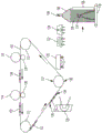
For example, as shown in fig. 1, an exemplary three-dimensional (3-D) printer includes, among other components, an intermediate transfer belt 110(ITB) supported on a roller 112, a first printing component (e.g., a developing device 116), and a second printing component (e.g., a developing device 114). Thus, as shown in fig. 1, first printing component 116 is positioned to electrostatically transfer (via a charge difference between the belt (e.g., generated by charge generator 128) and the material being transferred) first material 104, a build material, e.g., a (possibly dry) powdered polymer-wax material (e.g., charged 3-D toner), to ITB 110. A second printing component 114 (which may also be, for example, a photoreceptor) is also positioned to transfer a second material 105 (e.g., a support material, such as a powdered polymer-wax material (e.g., charged 3-D toner)) to the location of the ITB110, where the first material 104 is located on the ITB 110.
The build material 104 has a higher melting temperature than the support material 105 to allow the printed 3-D structure 104 to be separated from the support material 105 after the complete 3-D project is completed. For example, the melting temperature of the build material may be 25%, 50%, 75%, etc. above the melting temperature of the support material relative to any temperature (e.g., room temperature (20 ℃) or the melting temperature of ice (0 ℃); or may be 2 times, 5 times, 10 times, etc. the melting temperature of the support material. Thus, in one example, the support material may melt at 100 ℃ while the build material may melt at about 200 ℃. Further, the build and support materials may be made of any substance that is capable of being processed by an electrostatic printing process, whether such materials are currently known or developed in the future. For example, the build and support materials may be polymers, plastics, metals, ceramics, silicon-based materials, carbon-based materials, sugars, and the like.
In the figures, the combination of build material 104 and support material 105 is shown as element 102 and is sometimes referred to as a "development layer". The developed layer 102 of build material 104 and support material 105 is on discrete areas of the ITB110 and in a pattern corresponding to the components of the 3-D structure in the layer (and its associated support elements) where the 3-D structure is being built, the layer 102 being formed from the developed layer 102.
Further, a platen 118 (which may be a surface or a belt) is adjacent to the ITB 110. In this example, the platen 118 is a vacuum belt. The patterned layer of build and support material 102 is transferred from the developing devices 114, 116 to the intermediate transfer belt 110 and ultimately to the platen 118 at the injection station 130.
As shown in fig. 1, the implant station 130 is adjacent to the ITB 110. The injection station 130 includes rollers 112 that support the ITB110 on one side of the ITB 110. The injection station 130 is positioned to receive the layer 102 when the ITB110 is moved to the injection station 130. More specifically, the build material development station 116, support material development station 114, and injection station 130 are positioned relative to the ITB110 such that as the ITB110 moves in the process direction, the layer 102 on the ITB110 passes first through the build and support material development stations 114, 116 and then through the injection station 130.
As further shown in fig. 1, such structures may include heaters 120, 126 and bonding stations 122, 124. The bonding stages 122, 124 are positioned to apply light (e.g., UV light) using the light source 124 and/or to be heated using the light source 124. The structure may also include a support material removal station 148 discussed below.
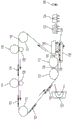
As indicated by the vertical arrows in fig. 2, the platen 118 is moved toward the ITB110 (using motors, gears, pulleys, cables, guides, etc. (all generally indicated by item 118)) to bring the platen 118 into contact with the ITB 110. The developed layer 102 and ITB110 may optionally be locally heated by a heater 120 to further assist in placing the developed layer 102 in a "tacky" state prior to implantation. In one example, the development layer 102 may be heated to a temperature above the glass transition temperature (Tg) but below the melting temperature (Tm) of the support material to render the support material (and possibly the build material) tacky.
Thus, patterned build and support material electrostatically printed on the ITB by each individual development device 114, 116 is bonded together in the development layer 102 to represent a particular pattern having a predetermined length. Thus, as shown in fig. 2, each developed layer 102 has a leading edge 134 oriented toward the process direction of movement of the ITB110 (indicated by the arrow near the ITB 110) and a trailing edge 136 opposite the leading edge 134.
More specifically, as shown in FIG. 2, at injection nip 130, leading edge 134 of development layer 102 within injection nip 130 begins to transfer to a corresponding location of platen 118. Thus, in fig. 2, platen 118 moves into contact with development layer 102 on ITB110 at a location where leading edge 134 of development layer 102 is at the lowest position of the rollers of implant nip 130. Thus, in this example, trailing edge 136 of development layer 102 has not yet reached injection nip 130, and thus has not yet been transferred to platen 118.
As shown in fig. 3, by moving or rotating the platen vacuum belt, the platen 118 is moved in synchronization with the ITB110 (at the same speed and in the same direction as the ITB 110) so that the developed layer 102 is completely transferred to the platen 118 without stains. In fig. 3, trailing edge 136 of developer layer 102 is the only portion that has not yet reached injection nip 130 and thus has not been transferred to platen 118. Then, as the ITB110 moves in the process direction, the platen 118 moves at the same speed and in the same direction as the ITB110 until the trailing edge 136 of the developed layer 102 reaches the bottom of the rollers of the injection nip 130, at which point the platen 118 moves away from the ITB110 and reaches the heater 126, as shown in fig. 4 (the heater 126 may be a non-contact (e.g., an Infrared (IR) heater) or a pressure heater, such as a fuser roller, that heats the layer 102 to a temperature below the melting temperature of the build and support materials).
As shown in fig. 4 and 5, if the heater 126 is a pressure roller, the platen 118 moves in synchronization with the rotation of the roller, applying heat and pressure to fuse the developer layer 102 to the platen 118 (again, at a temperature below the melting temperature of the build and support material). This synchronized movement between the platen 118 and the ITB110 (and heater roller 126) results in the pattern of support and build material (102) printed by the development devices 116, 114 being accurately transferred from the ITB110 to the platen 118 without distortion or smudge.
After each transfer of each developed layer 102 to platen 118 by ITB110, platen 118 may be moved to heater 126 to independently heat each developed layer 102 and successively join each developed layer 102 to platen 118 and any previously transferred developed layers 102 on platen 118. In other alternatives, after a particular number (e.g., 2, 3, 4, etc.) of development layers 102 have been placed on platen 118, platen 118 may only be moved to heater 126 so that multiple development layers 102 are fused to platen 118 and to each other simultaneously.
Thus, the process in FIGS. 2-5 is repeated to fuse the plurality of developed layers 102 into a stack 106, as shown in FIG. 6. As the stack 106 of developed layers 102 grows, additional developed layers 102 are formed on top of the stack 106, as shown in fig. 6, and such additional developed layers 102 are pressurized and heated by the heater 126, as shown in fig. 7, to fuse all of the developed layers 102 within the stack 106 together.
As shown in fig. 8, the bonding stations 122, 124 are configured to apply light and/or heat to the 3-D structure to bond the developed layers 102 in the independent stacks 106 to each other on the platen 118. The selective use of heaters, lights and other components 122, 124 in conjunction with the stage will vary depending on the chemical composition of the developer layer 102.
In one example, build material 104 and support material 105 may be UV curable toners. Thus, as shown in fig. 8, in one example, the bonding stations 122, 124 may bond such materials 102 by heating the materials 102 to a temperature between their glass transition temperature and their melting temperature, and then applying UV light to crosslink the polymers within the materials 102, thereby creating a rigid structure. Those of ordinary skill in the art will appreciate that other construction and support materials will utilize other bonding processes and bonding components, and the foregoing is provided as only one limited example; and the apparatus and methods herein are applicable to all such bonding methods and components, whether presently known or developed in the future.
In one example, the bonding stations 122, 124 may apply such light and/or heat after each transfer of each developed layer 102 to the platen 118 by the ITB110, or less frequently, such as only once (e.g., when the entire stack 106 is fully formed). In addition, fig. 8 shows a cladding showing portions of the support material 105 and the build material 104 within the accumulation of the individual stacks 106. This may or may not be visible and is only shown to show one exemplary way in which such build and support materials may be arranged.
The 3-D structure of the individual stacks 106 may be exported to allow manual removal of the support material 105 using an external heating bath; or the treatment may be performed as shown in fig. 9-11. More specifically, in FIG. 9, the support material removal station 148 is positioned to receive the now bonded 3-D individual stack 106 on the platen 118. The support material removal station 148 applies heat 156 (e.g., in the form of heated air, heated water, heated solvent, infrared heat, etc.) to raise the temperature of the stack 106 to a temperature above the melting temperature of the support material 105 but below the melting temperature of the build material 104. This causes the support material 105 to melt without affecting the build material 104.
For example, the heat 156 shown in FIG. 9 may be heated liquid (which may be a solvent), heated gas, infrared heating, or the like. Again, as described above, the heat 156 used will depend on the chemical makeup of the build material 104 and the support material 105. Fig. 10 illustrates a process in which about half of the support material 105 remains, and a portion of the build material 104 protrudes from the remaining stack of support material 105. FIG. 11 shows that the support material removal station 148 has applied sufficient heat 156 to melt all of the support material 105, leaving only post-processing of the build material 104 that leaves a complete 3-D structure made only of the build material 104.
Fig. 12-13 illustrate an alternative 3-D electrostatic printing configuration herein that includes a planar implantation station 138 in place of the implantation clamp 130 shown in fig. 1. As shown in fig. 12, the planar injection station 138 is a planar portion of the ITB110 between the rollers 112 and parallel to the platen 118. With this configuration, as shown in fig. 13, when platen 118 is moved to contact planar implantation station 138, all of the developed layers 102 are simultaneously transferred to platen 118 or partially formed stack 106, avoiding the roll implantation process shown in fig. 2 and 3.
Similarly, as shown in fig. 14, a drum 158 may be used in place of the ITB110, with all other components operating as described herein. Thus, drum 158 may be an intermediate transfer surface that receives material from development stations 114, 116, as described above, or may be a photoreceptor and operate as photoreceptor 256 as described below, operating by holding a latent image of charge and receiving material from development device 254.
FIG. 15 shows many of the components of the 3-D printer architecture 204 herein. The 3-D printing device 204 includes a controller/tangible processor 224 and a communication port (input/output) 214 operatively connected to the tangible processor 224 and a computer network external to the printing device 204. Further, the printing device 204 may include at least one accessory feature, such as a Graphical User Interface (GUI) component 212. The user may receive messages, instructions, and menu options and enter instructions through a graphical user interface or control panel 212.
The input/output devices 214 are used for communication to and from the 3-D printing device 204 and include wired devices or wireless devices (in any form, whether now known or developed in the future). The tangible processor 224 controls various actions of the printing device 204. Non-transitory, tangible computer storage media devices 210 (which may be optical, magnetic, capacitor-based, etc., and other than transitory signals) are readable by a tangible processor 224 and store instructions that the tangible processor 224 executes to allow a computerized device to perform its various functions, such as those described herein. Thus, as shown in fig. 15, the main body housing has one or more functional components that operate on power provided by an Alternating Current (AC) source 220 provided by a power source 218. The power supply 218 may include a common power conversion unit, a power storage element (e.g., a battery, etc.), and the like.
The 3-D printing device 204 includes at least one marking device (print engine) 240 that deposits successive layers of build and support material as described above on the platen and is operably connected to a dedicated image processor 224 (which is different from a general purpose computer in that it is dedicated to processing image data). Moreover, the printing device 204 may include at least one accessory function (such as a scanner 232) that also operates on power supplied from the external power supply 220 (via the power supply 218).
The one or more print engines 240 are intended to illustrate any presently known or later developed marking device that applies build and support material (toner, etc.) and may include, for example, a device that uses the intermediate transfer belt 110 (as shown in fig. 16).
Thus, as shown in fig. 16, each print engine 240 shown in fig. 15 may utilize one or more potentially different (e.g., different colors, different materials, etc.) build material development stations 116, one or more potentially different (e.g., different colors, different materials, etc.) support material development stations 114, and so forth. The development stations 114, 116 may be any form of development station, whether currently known or developed in the future, such as a separate electrostatic marking station, a separate ink jet station, a separate dry ink station, etc. Each development station 114, 116 sequentially transfers material patterns to the same location of the intermediate transfer belt 110 during a single belt rotation (possibly independent of the condition of the intermediate transfer belt 110), thereby reducing the number of passes through the intermediate transfer belt 110 that must be made before a complete and complete image is transferred to the intermediate transfer belt 110. While fig. 16 shows five development stations adjacent to or in contact with the rotating belt (110), such an apparatus may use any number of marking stations (e.g., 2, 3, 5, 8, 11, etc.), as will be appreciated by one of ordinary skill in the art.
An exemplary separate electrostatic development station 114, 116 is shown in fig. 17 as being positioned adjacent to (or possibly in contact with) the intermediate transfer belt 110. Each individual electrostatic development station 114, 116 includes its own charging station 258 that produces a uniform charge on the internal photoreceptor 256, an internal exposure device 260 that patterns the uniform charge into a latent charge image, and an internal development device 254 that transfers the build or support material to the photoreceptor 256 in a pattern that matches the latent charge image. The pattern of build or support material is then pulled from the photoreceptor 256 to the intermediate transfer belt 110 by the opposite charge of the intermediate transfer belt 110 relative to the charge of the build or support material, which is typically generated by the charge generator 128 on the opposite side of the intermediate transfer belt 110.
FIG. 18 is a flow chart illustrating processing of a method performed herein. More specifically, such processes begin in item 170, where the methods electrostatically transfer the build and support materials to an intermediate transfer surface using a build material and support material development station. These processes transfer layers of build material and support material, each on discrete areas of the ITB and in a pattern, to an intermediate transfer surface.
In item 172, the developed layer and the previously transferred layer can optionally be heated to promote adhesion of the layers. Then, in item 174, such a method moves the intermediate transfer surface through the injection station and moves the platen relative to the intermediate transfer surface such that the platen contacts a layer on the intermediate transfer surface. Each time the platen contacts a layer on the intermediate transfer surface at the injection station in item 174, the intermediate transfer surface applies layers of build material and support material to the platen to successively form separate stacks of layers of build and support material on the platen. In item 174, the optional heat facilitates transfer of the layer from the intermediate transfer surface to the layer on the platen.
Such methods may optionally move a platen from the injection station to a heater to heat the layers and bond each layer together in item 176. Similarly, in item 176, the methods can move the platen to a pressure roller to laminate each together.
Item 178 shows these methods curing the stack of developed layers using a curing station. In various configurations, these methods use a heater or pressure roller (176) to bond the layers and/or a curing station (178) to cure the layers after each layer is transferred to the platen at the injection nip, or after a previously established number of layers are transferred to the platen at the injection nip. Thus, the set of (possibly all) developed layers may be bonded (176) and/or cured (178) simultaneously, or such bonding and curing may be performed layer-by-layer, and the sequence of operations shown in fig. 18 is not strictly followed.
As shown in item 180, such methods may also move the platen to a support material removal station positioned to heat the stack to a temperature above the melting temperature of the support material but below the melting temperature of the build material to melt the support material, but leave a 3-D structure made only of the build material.
Fig. 19 is an expanded view showing how development layers 102 may contain some build material 104 and some support material 105, and how the lowest development layer 102 is bonded to platen 118, and how each successive development layer 102 contacts and is bonded to the immediately preceding adjacent development layer 102, which is below to form stack 106 of development layers 102 on platen 118. As described above, the particles of build material 104 and support material 105 (shown as particles (not drawn to scale) in fig. 19, using reference numeral 102) within the development layer 102 are sticky particles of powder that connect to the sticky top development layer 102.
Although some example structures are shown in the drawings, those of ordinary skill in the art will understand that the drawings are simplified schematic diagrams and that the claims set forth below include many features that are not shown (or possibly much fewer), but are often used with such devices and systems. Accordingly, applicants do not intend the claims set forth below to be limited by the drawings, but rather the drawings are provided solely to illustrate the several ways in which the claimed features can be implemented.
As shown in US 8,488,994, additive manufacturing systems for printing 3-D parts using electrophotography are known. The system includes a photoconductor component having a surface and a development station, wherein the development station is configured to develop a layer of material on the surface of the photoconductor component. The system also includes a transfer medium configured to receive the development layer from the surface of the rotatable photoconductive member, and a platen configured to receive the development layer from the transfer member in a layer-by-layer manner to print the 3D member from at least a portion of the received layer.
With respect to UV curable toners, as disclosed in US 7,250,238, it is known to provide UV curable toner compositions, and methods of using UV curable toner compositions in printing processes. US 7,250,238 discloses various toner emulsion aggregation processes that allow the toners produced in the examples to be cured, i.e., by exposure to UV radiation, e.g., UV light having a wavelength of from about 100nm to about 400 nm. In US 7,250,238, the produced toner composition can be used in various printing applications, such as temperature sensitive packaging and producing foil seals. In US 7,250,238, the examples relate to UV curable toner compositions consisting of: an optional colorant, an optional wax, a polymer derived from styrene, and an acrylate selected from butyl acrylate, carboxyethyl acrylate, and a UV curable acrylate oligomer. In addition, these aspects relate to toner compositions comprised of colorants, such as pigments, optional waxes, and polymers produced from UV curable cycloaliphatic epoxides.
Further, US 7,250,238 discloses a method of forming a UV curable toner composition comprising mixing an emulsion containing a polymer formed from styrene, butyl acrylate, carboxymethyl acrylate and a UV curable acrylate with a colorant and a wax; adding a flocculating agent to the mixture to optionally induce aggregation and form toner precursor particles dispersed in the second mixture; heating the toner precursor particles to a temperature equal to or higher than the glass transition temperature (Tg) of the polymer to form toner particles; optionally washing the toner particles; and optionally drying the toner particles. Another aspect relates to toner particles prepared by the method.
Although some example structures are shown in the drawings, those of ordinary skill in the art will understand that the drawings are simplified schematic diagrams and that the claims set forth below include many features that are not shown (or possibly much fewer), but are often used with such devices and systems. Accordingly, applicants do not intend the claims set forth below to be limited by the drawings, but rather the drawings are provided solely to illustrate the several ways in which the claimed features can be implemented.
Many computerized devices are discussed above. Computerized devices including chip-based Central Processing Units (CPUs), input/output devices (including Graphical User Interfaces (GUIs), memories, comparators, tangible processors, etc.) produced by manufacturers such as dell computers, Round Rock TX, usa, and apple computer, Cupertino CA, usa, are well known and readily available devices. Such computerized devices typically include input/output devices, power supplies, tangible processors, electronic storage memory, wiring, and the like, the details of which have been omitted herein to allow the reader to focus on the salient aspects of the systems and methods described herein. Similarly, printers, copiers, scanners and other similar peripheral devices are available from Xerox corporation, Norwalk, CT, USA, and the details of such devices are not discussed herein for the sake of brevity and reader's attention.
The term printer or printing apparatus as used herein includes any device that performs a printout function for any purpose, such as a digital copier, collector, facsimile machine, multi-function machine, etc. The details of printers, print engines, etc. are well known and are not described in detail herein to focus the disclosure on the salient features presented. The systems and methods herein may include systems and methods for printing in color, monochrome, or processing color or monochrome image data. All of the above systems and methods are particularly applicable to xerographic and/or xerographic machines and/or processes.
For the purposes of the present invention, the term "fixing" refers to drying, hardening, polymerization, crosslinking, bonding or addition reactions or other reactions of the coating. Furthermore, terms used herein, such as "right," "left," "vertical," "horizontal," "top," "bottom," "upper," "lower," "below," "beneath," "above," "parallel," "vertical," and the like, are to be understood as relative positions as they are oriented and shown in the drawings (unless otherwise specified). Terms such as "contacting," "over," "directly contacting," "abutting," "directly adjacent to," and the like, mean that at least one element physically contacts another element (without the other elements separating the elements). Further, the terms automatic or automatically refer to once a process is started (by a machine or user), one or more machines performing the process without further input from any user. In the drawings herein, like reference numerals identify the same or similar items.
It will be appreciated that the above-disclosed and other features and functions, or alternatives thereof, may be desirably combined into many other different systems or applications. Various presently unforeseen or unanticipated alternatives, modifications, variations or improvements therein may be subsequently made by those skilled in the art which are also intended to be encompassed by the following claims. No limitations to any particular order, quantity, position, size, shape, angle, color, or material may be implied or implied from any such example by the steps or components of the systems and methods herein unless specifically recited in a particular claim.
Claims (18)
1. A three-dimensional printer comprising:
an intermediate transfer surface;
a build material development station positioned to electrostatically transfer build material to the intermediate transfer surface;
a support material development station positioned to electrostatically transfer support material to the intermediate transfer surface, the build material having a higher melting temperature than the support material, the build material development station and the support material development station transferring layers of the build material and the support material then having the higher melting temperature to the intermediate transfer surface;
an injection station adjacent the intermediate transfer surface, the injection station positioned to receive the layer as the intermediate transfer surface moves past the injection station;
a platen moving relative to the intermediate transfer surface, the intermediate transfer surface transferring layers of the build material and the support material to the platen each time the platen contacts one of the layers on the intermediate transfer surface at the injection station to successively form separate stacks of the layers on the platen;
a curing station positioned to apply UV light to the entire layers to cure the layers to each other; and
a support material removal station configured and positioned to heat the individual stacks to a temperature above a melting temperature of the support material but below a melting temperature of the build material to leave a three-dimensional structure made only of the build material.
2. The three-dimensional printer according to claim 1, further comprising a surface heater positioned to direct heat at the injection station, the surface heater heating the intermediate transfer surface and the platen at the injection station.
3. The three-dimensional printer according to claim 2, said layer being tacky after exposure to said heat, which facilitates transfer of said layer from said intermediate transfer surface to said layer on said platen.
4. The three-dimensional printer of claim 1, the build material development station, the support material development station, and the injection station being positioned relative to the intermediate transfer surface such that a point on the intermediate transfer surface passes first through the build material development station and the support material development station and then through the injection station as the intermediate transfer surface moves in a process direction.
5. The three-dimensional printer according to claim 1, further comprising a heater adjacent to the platen, the platen moving from the injection station to the heater to heat the layers and join each of the layers together; and
a pressure roller adjacent to the heater, the platen moving to the pressure roller to press each of the plies together.
6. The three-dimensional printer according to claim 1, the build material and the support material comprising a polymer and the curing station positioned to couple the polymer in the build material and the support material.
7. A three-dimensional printer comprising:
an intermediate transfer belt;
a build material development station positioned to electrostatically transfer build material to the intermediate transfer belt;
a support material development station positioned to electrostatically transfer support material to a location of the intermediate transfer belt, wherein the build material is on the intermediate transfer belt, the build material has a higher melting temperature than the support material, the build material development station and the support material development station transfer layers of the build material and the support material, each of the layers being on a discrete area of the intermediate transfer belt and in a pattern, to the intermediate transfer belt then having the higher melting temperature;
an injection station adjacent to the intermediate transfer belt, the injection station including a roller supporting the intermediate transfer belt on a first side of the intermediate transfer belt, the injection station positioned to receive the layers as the intermediate transfer belt moves past the injection station;
a platen moving relative to the intermediate transfer belt, the intermediate transfer belt transferring the build material and the layer of support material to the platen each time the platen contacts one of the layers on a second side of the intermediate transfer belt at the injection station to successively form separate stacks of the layers on the platen, the first side being opposite the second side;
a support material removal station configured and positioned to heat the individual stacks to a temperature above a melting temperature of the support material but below a melting temperature of the build material to leave a three-dimensional structure made only of the build material; and
a curing station positioned to apply UV light to the entire layers to cure the layers to each other.
8. The three-dimensional printer according to claim 7, further comprising a surface heater positioned to direct heat at the injection station, the surface heater heating the intermediate transfer belt and the platen at the injection station.
9. The three-dimensional printer according to claim 8, said layer being tacky after exposure to said heat, which facilitates transfer of said layer from said intermediate transfer belt to said layer on said platen.
10. The three-dimensional printer of claim 7, the build material development station, the support material development station, and the injection station being positioned relative to the intermediate transfer belt such that a point on the intermediate transfer belt passes first through the build material development station and the support material development station and then through the injection station as the intermediate transfer belt moves in a process direction.
11. The three-dimensional printer according to claim 7, further comprising a heater adjacent the platen, the platen moving from the injection station to the heater to heat the layers and join each of the layers together; and
a pressure roller adjacent to the heater, the platen moving to the pressure roller to press each of the plies together.
12. The three-dimensional printer according to claim 7, the build material and the support material comprising a polymer and the curing station positioned to couple the polymer in the build material and the support material.
13. A three-dimensional printer comprising:
an intermediate transfer surface;
a build material development station specifically designated to process only build material, the build material development station positioned to electrostatically transfer only the build material to the intermediate transfer surface;
a support material development station specifically designated to process only support material, the support material development station positioned to electrostatically transfer only the support material to the intermediate transfer surface, the build material having a higher melting temperature than the support material, the build material development station and the support material development station transferring layers of the build material and the support material then having the higher melting temperature to the intermediate transfer surface;
an injection station adjacent the intermediate transfer surface, the injection station positioned to receive the layer as the intermediate transfer surface moves past the injection station;
a platen moving relative to the intermediate transfer surface, the intermediate transfer surface transferring layers of the build material and the support material to the platen each time the platen contacts one of the layers on the intermediate transfer surface at the injection station to successively form separate stacks of the layers on the platen;
a curing station positioned to apply UV light to the entire layers to cure the layers to each other; and
a support material removal station configured and positioned to heat the individual stacks to a temperature above a melting temperature of the support material but below a melting temperature of the build material to leave a three-dimensional structure made only of the build material.
14. The three-dimensional printer according to claim 13, further comprising a surface heater positioned to direct heat at the injection station, the surface heater heating the intermediate transfer surface and the platen at the injection station.
15. The three-dimensional printer according to claim 14, said layer being tacky after exposure to said heat, which facilitates transfer of said layer from said intermediate transfer surface to said layer on said platen.
16. The three-dimensional printer according to claim 13, the build material development station, the support material development station, and the injection station being positioned relative to the intermediate transfer surface such that a point on the intermediate transfer surface passes first through the build material development station and the support material development station and then through the injection station as the intermediate transfer surface moves in a process direction.
17. The three-dimensional printer according to claim 13, further comprising a heater adjacent the platen, the platen moving from the injection station to the heater to heat the layers and join each of the layers together; and
a pressure roller adjacent to the heater, the platen moving to the pressure roller to press each of the plies together.
18. The three-dimensional printer according to claim 13, the build material and the support material comprising a polymer and the curing station positioned to couple the polymer in the build material and the support material.
Applications Claiming Priority (2)
| Application Number | Priority Date | Filing Date | Title |
|---|---|---|---|
| US15/152,659 US10195787B2 (en) | 2016-05-12 | 2016-05-12 | Electrostatic 3-D development apparatus using different melting point materials |
| US15/152659 | 2016-05-12 |
Publications (2)
| Publication Number | Publication Date |
|---|---|
| CN107364122A CN107364122A (en) | 2017-11-21 |
| CN107364122B true CN107364122B (en) | 2020-01-21 |
Family
ID=58671484
Family Applications (1)
| Application Number | Title | Priority Date | Filing Date |
|---|---|---|---|
| CN201710259351.8A Active CN107364122B (en) | 2016-05-12 | 2017-04-19 | Electrostatic three-dimensional developing device using materials with different melting points |
Country Status (5)
| Country | Link |
|---|---|
| US (1) | US10195787B2 (en) |
| EP (1) | EP3243659B1 (en) |
| JP (1) | JP6824100B2 (en) |
| KR (1) | KR102159478B1 (en) |
| CN (1) | CN107364122B (en) |
Families Citing this family (5)
| Publication number | Priority date | Publication date | Assignee | Title |
|---|---|---|---|---|
| US11273608B2 (en) * | 2018-06-07 | 2022-03-15 | Sakuu Corporation | Multi-material three-dimensional printer |
| CN114364512A (en) * | 2019-07-03 | 2022-04-15 | 进化添加剂解决方案股份有限公司 | Selective deposition based additive manufacturing using different materials |
| EP3993988A4 (en) * | 2019-07-03 | 2023-07-26 | Evolve Additive Solutions, Inc. | Selective layer deposition based additive manufacturing system using laser nip heating |
| US11440263B2 (en) * | 2019-12-23 | 2022-09-13 | Cubicure Gmbh | System for the lithography-based additive manufacturing of three-dimensional (3D) structures |
| CN116096554A (en) * | 2020-07-15 | 2023-05-09 | 进化添加剂解决方案股份有限公司 | Additive manufacturing method using reduced support material |
Family Cites Families (53)
| Publication number | Priority date | Publication date | Assignee | Title |
|---|---|---|---|---|
| US4100884A (en) | 1976-02-25 | 1978-07-18 | Ricoh Company, Ltd. | Rubber developer roller using single component toner |
| US4063808A (en) | 1976-03-23 | 1977-12-20 | International Business Machines Corporation | Apparatus for neutralizing toner in a no charge exchange transfer |
| JPS53113549A (en) | 1977-03-15 | 1978-10-04 | Fuji Photo Film Co Ltd | Marking device |
| US4510223A (en) | 1983-02-07 | 1985-04-09 | Coulter Systems Corporation | Multicolor electrophotographic imaging process |
| US5103263A (en) | 1989-05-23 | 1992-04-07 | Delphax Systems | Powder transport, fusing and imaging apparatus |
| US5088047A (en) * | 1989-10-16 | 1992-02-11 | Bynum David K | Automated manufacturing system using thin sections |
| US5016055A (en) | 1990-07-02 | 1991-05-14 | Xerox Corporation | Method and apparatus for using vibratory energy with application of transfer field for enhanced transfer in electrophotographic imaging |
| US4987456A (en) | 1990-07-02 | 1991-01-22 | Xerox Corporation | Vacuum coupling arrangement for applying vibratory motion to a flexible planar member |
| US5282006A (en) | 1992-12-07 | 1994-01-25 | Xerox Corporation | Transfer system including pre-transfer pressure treatment apparatus |
| US5339147A (en) | 1993-11-24 | 1994-08-16 | Xerox Corporation | Sequential ultrasonic fusing process |
| US5477315A (en) | 1994-07-05 | 1995-12-19 | Xerox Corporation | Electrostatic coupling force arrangement for applying vibratory motion to a flexible planar member |
| US5966559A (en) | 1997-09-23 | 1999-10-12 | Eastman Kodak Company | Method and apparatus for sensing and accomodating different thickness paper stocks in an electrostatographic machine |
| US6066285A (en) | 1997-12-12 | 2000-05-23 | University Of Florida | Solid freeform fabrication using power deposition |
| US6141524A (en) | 1999-07-26 | 2000-10-31 | Xerox Corporation | Release agent management for transfuse systems |
| US6157804A (en) | 2000-03-22 | 2000-12-05 | Xerox Corporation | Acoustic transfer assist driver system |
| US6376148B1 (en) * | 2001-01-17 | 2002-04-23 | Nanotek Instruments, Inc. | Layer manufacturing using electrostatic imaging and lamination |
| US6775504B2 (en) | 2002-12-16 | 2004-08-10 | Xerox Corporation | Developer member adapted for depositing developer material on an imaging surface |
| US7250238B2 (en) | 2003-12-23 | 2007-07-31 | Xerox Corporation | Toners and processes thereof |
| US7184698B2 (en) | 2004-03-17 | 2007-02-27 | Eastman Kodak Company | Durable electrophotographic prints |
| US7270408B2 (en) | 2005-01-14 | 2007-09-18 | Xerox Corporation | Low level cure transfuse assist for printing with radiation curable ink |
| US20080131800A1 (en) | 2006-12-02 | 2008-06-05 | Xerox Corporation | Toners and toner methods |
| WO2008075252A1 (en) * | 2006-12-19 | 2008-06-26 | Koninklijke Philips Electronics N.V. | Imaging of a turbid medium |
| WO2008118263A1 (en) * | 2007-03-22 | 2008-10-02 | Stratasys, Inc. | Extrusion-based layered deposition systems using selective radiation exposure |
| US7851549B2 (en) | 2007-12-13 | 2010-12-14 | Xerox Corporation | Curable polyester latex made by phase inversion emulsification |
| US20100140852A1 (en) | 2008-12-04 | 2010-06-10 | Objet Geometries Ltd. | Preparation of building material for solid freeform fabrication |
| US20100227184A1 (en) | 2009-03-06 | 2010-09-09 | Xerox Corporation | Photoreceptor transfer belt and method for making the same |
| US8470231B1 (en) | 2009-06-01 | 2013-06-25 | Stratasys Ltd. | Three-dimensional printing process for producing a self-destructible temporary structure |
| US8306443B2 (en) | 2009-06-26 | 2012-11-06 | Xerox Corporation | Multi-color printing system and method for reducing the transfer field through closed-loop controls |
| US8265536B2 (en) | 2010-08-12 | 2012-09-11 | Xerox Corporation | Fixing systems including contact pre-heater and methods for fixing marking material to substrates |
| US8396404B2 (en) | 2010-08-26 | 2013-03-12 | Xerox Corporation | Image transfer nip method and apparatus using constant current controls |
| US8548621B2 (en) | 2011-01-31 | 2013-10-01 | Xerox Corporation | Production system control model updating using closed loop design of experiments |
| EP2541481A1 (en) * | 2011-07-01 | 2013-01-02 | TeliaSonera AB | Personalized advertising |
| US8879957B2 (en) | 2011-09-23 | 2014-11-04 | Stratasys, Inc. | Electrophotography-based additive manufacturing system with reciprocating operation |
| US20130186558A1 (en) | 2011-09-23 | 2013-07-25 | Stratasys, Inc. | Layer transfusion with heat capacitor belt for additive manufacturing |
| US8488994B2 (en) | 2011-09-23 | 2013-07-16 | Stratasys, Inc. | Electrophotography-based additive manufacturing system with transfer-medium service loops |
| US9885987B2 (en) * | 2011-09-23 | 2018-02-06 | Stratasys, Inc. | Layer transfusion for additive manufacturing |
| US8836911B2 (en) | 2011-10-17 | 2014-09-16 | Xerox Corporation | Method and system for producing flat three-dimensional images |
| CN108381909B (en) | 2012-11-09 | 2021-05-25 | 赢创运营有限公司 | Use and preparation of coated filaments for extrusion 3D printing processes |
| EP2917026A1 (en) | 2012-11-09 | 2015-09-16 | Evonik Röhm GmbH | Multicoloured extrusion-based 3d printing |
| US9029058B2 (en) | 2013-07-17 | 2015-05-12 | Stratasys, Inc. | Soluble support material for electrophotography-based additive manufacturing |
| US20150024317A1 (en) | 2013-07-17 | 2015-01-22 | Stratasys, Inc. | High-Performance Consumable Materials for Electrophotography-Based Additive Manufacturing |
| US9144940B2 (en) | 2013-07-17 | 2015-09-29 | Stratasys, Inc. | Method for printing 3D parts and support structures with electrophotography-based additive manufacturing |
| CN105722663B (en) | 2013-11-18 | 2019-05-21 | 张凯瑞 | Colored or more material 3D printers |
| US9744730B2 (en) | 2013-11-22 | 2017-08-29 | Stratasys, Inc. | Magnetic platen assembly for additive manufacturing system |
| WO2015133641A1 (en) | 2014-03-07 | 2015-09-11 | Canon Kabushiki Kaisha | Method of producing three-dimensional shaped article |
| US10144175B2 (en) | 2014-03-18 | 2018-12-04 | Evolve Additive Solutions, Inc. | Electrophotography-based additive manufacturing with solvent-assisted planarization |
| US9770869B2 (en) | 2014-03-18 | 2017-09-26 | Stratasys, Inc. | Additive manufacturing with virtual planarization control |
| US9694541B2 (en) | 2014-06-09 | 2017-07-04 | Raytheon Company | Selective composite manufacturing for components having multiple material properties |
| US10272618B2 (en) | 2015-02-23 | 2019-04-30 | Xactiv, Inc. | Fabrication of 3D objects via electrostatic powder deposition |
| CN104890241B (en) | 2015-06-03 | 2017-06-06 | 珠海天威飞马打印耗材有限公司 | Three-dimensional fast shaping equipment and forming method |
| US20170029997A1 (en) * | 2015-07-27 | 2017-02-02 | Juliette H Silver | Method and Device for Maintaining Constant Moisture Level in Cleaning Cloths |
| US10792908B2 (en) | 2015-12-31 | 2020-10-06 | Evolve Additive Solutions, Inc. | Systems and methods for electrophotography-based additive manufacturing of parts |
| US10105902B2 (en) * | 2016-04-18 | 2018-10-23 | Evolve Additive Solutions, Inc. | Electrophotography-based additive manufacturing with part molding |
-
2016
- 2016-05-12 US US15/152,659 patent/US10195787B2/en active Active
-
2017
- 2017-04-19 CN CN201710259351.8A patent/CN107364122B/en active Active
- 2017-04-20 KR KR1020170051098A patent/KR102159478B1/en active IP Right Grant
- 2017-04-21 JP JP2017084589A patent/JP6824100B2/en active Active
- 2017-05-04 EP EP17169602.4A patent/EP3243659B1/en active Active
Also Published As
| Publication number | Publication date |
|---|---|
| JP2017202682A (en) | 2017-11-16 |
| US20170326796A1 (en) | 2017-11-16 |
| EP3243659B1 (en) | 2020-07-08 |
| CN107364122A (en) | 2017-11-21 |
| KR102159478B1 (en) | 2020-09-25 |
| US10195787B2 (en) | 2019-02-05 |
| EP3243659A1 (en) | 2017-11-15 |
| JP6824100B2 (en) | 2021-02-03 |
| KR20170128086A (en) | 2017-11-22 |
Similar Documents
| Publication | Publication Date | Title |
|---|---|---|
| CN107364122B (en) | Electrostatic three-dimensional developing device using materials with different melting points | |
| US11130282B2 (en) | Electrostatic 3-D development apparatus using cold fusing | |
| EP3255504B1 (en) | Electrostatic 3-d printer system using leveling material and mechanical planer | |
| US10086558B2 (en) | 3-D electrostatic printer using track bound platens and registration system | |
| CN107297895B (en) | Electrophotographic 3-D printing using dissolvable paper | |
| JP2017193170A (en) | Electro-photographic 3-d printing using collapsible substrate | |
| CN107364124B (en) | 3-D printing using intermediate transfer belt and curable polymer | |
| CN107364123B (en) | Electrostatic 3-D printer using addressable UV cross-linking | |
| US10279577B2 (en) | Electrostatic 3-D printer having rotating magnetic cores within developer rolls | |
| US10000010B2 (en) | 3-D electrostatic printer using rack and pinion registration system | |
| US10213958B2 (en) | Electrostatic 3-D printing system having acoustic transfer and corotron |
Legal Events
| Date | Code | Title | Description |
|---|---|---|---|
| PB01 | Publication | ||
| PB01 | Publication | ||
| SE01 | Entry into force of request for substantive examination | ||
| SE01 | Entry into force of request for substantive examination | ||
| GR01 | Patent grant | ||
| GR01 | Patent grant |