JP2017200739A - Resin laminate and touch input device including the same - Google Patents
Resin laminate and touch input device including the same Download PDFInfo
- Publication number
- JP2017200739A JP2017200739A JP2016093089A JP2016093089A JP2017200739A JP 2017200739 A JP2017200739 A JP 2017200739A JP 2016093089 A JP2016093089 A JP 2016093089A JP 2016093089 A JP2016093089 A JP 2016093089A JP 2017200739 A JP2017200739 A JP 2017200739A
- Authority
- JP
- Japan
- Prior art keywords
- resin
- layer
- input device
- touch input
- resin layer
- Prior art date
- Legal status (The legal status is an assumption and is not a legal conclusion. Google has not performed a legal analysis and makes no representation as to the accuracy of the status listed.)
- Pending
Links
Images


Classifications
-
- G—PHYSICS
- G06—COMPUTING; CALCULATING OR COUNTING
- G06F—ELECTRIC DIGITAL DATA PROCESSING
- G06F3/00—Input arrangements for transferring data to be processed into a form capable of being handled by the computer; Output arrangements for transferring data from processing unit to output unit, e.g. interface arrangements
- G06F3/01—Input arrangements or combined input and output arrangements for interaction between user and computer
- G06F3/03—Arrangements for converting the position or the displacement of a member into a coded form
- G06F3/041—Digitisers, e.g. for touch screens or touch pads, characterised by the transducing means
-
- B—PERFORMING OPERATIONS; TRANSPORTING
- B32—LAYERED PRODUCTS
- B32B—LAYERED PRODUCTS, i.e. PRODUCTS BUILT-UP OF STRATA OF FLAT OR NON-FLAT, e.g. CELLULAR OR HONEYCOMB, FORM
- B32B7/00—Layered products characterised by the relation between layers; Layered products characterised by the relative orientation of features between layers, or by the relative values of a measurable parameter between layers, i.e. products comprising layers having different physical, chemical or physicochemical properties; Layered products characterised by the interconnection of layers
- B32B7/04—Interconnection of layers
- B32B7/12—Interconnection of layers using interposed adhesives or interposed materials with bonding properties
-
- B—PERFORMING OPERATIONS; TRANSPORTING
- B32—LAYERED PRODUCTS
- B32B—LAYERED PRODUCTS, i.e. PRODUCTS BUILT-UP OF STRATA OF FLAT OR NON-FLAT, e.g. CELLULAR OR HONEYCOMB, FORM
- B32B27/00—Layered products comprising a layer of synthetic resin
- B32B27/06—Layered products comprising a layer of synthetic resin as the main or only constituent of a layer, which is next to another layer of the same or of a different material
- B32B27/08—Layered products comprising a layer of synthetic resin as the main or only constituent of a layer, which is next to another layer of the same or of a different material of synthetic resin
-
- B—PERFORMING OPERATIONS; TRANSPORTING
- B32—LAYERED PRODUCTS
- B32B—LAYERED PRODUCTS, i.e. PRODUCTS BUILT-UP OF STRATA OF FLAT OR NON-FLAT, e.g. CELLULAR OR HONEYCOMB, FORM
- B32B27/00—Layered products comprising a layer of synthetic resin
- B32B27/30—Layered products comprising a layer of synthetic resin comprising vinyl (co)polymers; comprising acrylic (co)polymers
- B32B27/302—Layered products comprising a layer of synthetic resin comprising vinyl (co)polymers; comprising acrylic (co)polymers comprising aromatic vinyl (co)polymers, e.g. styrenic (co)polymers
-
- B—PERFORMING OPERATIONS; TRANSPORTING
- B32—LAYERED PRODUCTS
- B32B—LAYERED PRODUCTS, i.e. PRODUCTS BUILT-UP OF STRATA OF FLAT OR NON-FLAT, e.g. CELLULAR OR HONEYCOMB, FORM
- B32B27/00—Layered products comprising a layer of synthetic resin
- B32B27/30—Layered products comprising a layer of synthetic resin comprising vinyl (co)polymers; comprising acrylic (co)polymers
- B32B27/308—Layered products comprising a layer of synthetic resin comprising vinyl (co)polymers; comprising acrylic (co)polymers comprising acrylic (co)polymers
-
- B—PERFORMING OPERATIONS; TRANSPORTING
- B32—LAYERED PRODUCTS
- B32B—LAYERED PRODUCTS, i.e. PRODUCTS BUILT-UP OF STRATA OF FLAT OR NON-FLAT, e.g. CELLULAR OR HONEYCOMB, FORM
- B32B27/00—Layered products comprising a layer of synthetic resin
- B32B27/32—Layered products comprising a layer of synthetic resin comprising polyolefins
- B32B27/325—Layered products comprising a layer of synthetic resin comprising polyolefins comprising polycycloolefins
-
- B—PERFORMING OPERATIONS; TRANSPORTING
- B32—LAYERED PRODUCTS
- B32B—LAYERED PRODUCTS, i.e. PRODUCTS BUILT-UP OF STRATA OF FLAT OR NON-FLAT, e.g. CELLULAR OR HONEYCOMB, FORM
- B32B27/00—Layered products comprising a layer of synthetic resin
- B32B27/36—Layered products comprising a layer of synthetic resin comprising polyesters
- B32B27/365—Layered products comprising a layer of synthetic resin comprising polyesters comprising polycarbonates
-
- B—PERFORMING OPERATIONS; TRANSPORTING
- B32—LAYERED PRODUCTS
- B32B—LAYERED PRODUCTS, i.e. PRODUCTS BUILT-UP OF STRATA OF FLAT OR NON-FLAT, e.g. CELLULAR OR HONEYCOMB, FORM
- B32B3/00—Layered products comprising a layer with external or internal discontinuities or unevennesses, or a layer of non-planar form; Layered products having particular features of form
- B32B3/02—Layered products comprising a layer with external or internal discontinuities or unevennesses, or a layer of non-planar form; Layered products having particular features of form characterised by features of form at particular places, e.g. in edge regions
- B32B3/08—Layered products comprising a layer with external or internal discontinuities or unevennesses, or a layer of non-planar form; Layered products having particular features of form characterised by features of form at particular places, e.g. in edge regions characterised by added members at particular parts
- B32B3/085—Layered products comprising a layer with external or internal discontinuities or unevennesses, or a layer of non-planar form; Layered products having particular features of form characterised by features of form at particular places, e.g. in edge regions characterised by added members at particular parts spaced apart pieces on the surface of a layer
-
- B—PERFORMING OPERATIONS; TRANSPORTING
- B32—LAYERED PRODUCTS
- B32B—LAYERED PRODUCTS, i.e. PRODUCTS BUILT-UP OF STRATA OF FLAT OR NON-FLAT, e.g. CELLULAR OR HONEYCOMB, FORM
- B32B3/00—Layered products comprising a layer with external or internal discontinuities or unevennesses, or a layer of non-planar form; Layered products having particular features of form
- B32B3/26—Layered products comprising a layer with external or internal discontinuities or unevennesses, or a layer of non-planar form; Layered products having particular features of form characterised by a particular shape of the outline of the cross-section of a continuous layer; characterised by a layer with cavities or internal voids ; characterised by an apertured layer
- B32B3/30—Layered products comprising a layer with external or internal discontinuities or unevennesses, or a layer of non-planar form; Layered products having particular features of form characterised by a particular shape of the outline of the cross-section of a continuous layer; characterised by a layer with cavities or internal voids ; characterised by an apertured layer characterised by a layer formed with recesses or projections, e.g. hollows, grooves, protuberances, ribs
-
- G—PHYSICS
- G06—COMPUTING; CALCULATING OR COUNTING
- G06F—ELECTRIC DIGITAL DATA PROCESSING
- G06F3/00—Input arrangements for transferring data to be processed into a form capable of being handled by the computer; Output arrangements for transferring data from processing unit to output unit, e.g. interface arrangements
- G06F3/01—Input arrangements or combined input and output arrangements for interaction between user and computer
- G06F3/03—Arrangements for converting the position or the displacement of a member into a coded form
- G06F3/041—Digitisers, e.g. for touch screens or touch pads, characterised by the transducing means
- G06F3/044—Digitisers, e.g. for touch screens or touch pads, characterised by the transducing means by capacitive means
- G06F3/0443—Digitisers, e.g. for touch screens or touch pads, characterised by the transducing means by capacitive means using a single layer of sensing electrodes
-
- G—PHYSICS
- G06—COMPUTING; CALCULATING OR COUNTING
- G06F—ELECTRIC DIGITAL DATA PROCESSING
- G06F3/00—Input arrangements for transferring data to be processed into a form capable of being handled by the computer; Output arrangements for transferring data from processing unit to output unit, e.g. interface arrangements
- G06F3/01—Input arrangements or combined input and output arrangements for interaction between user and computer
- G06F3/03—Arrangements for converting the position or the displacement of a member into a coded form
- G06F3/041—Digitisers, e.g. for touch screens or touch pads, characterised by the transducing means
- G06F3/044—Digitisers, e.g. for touch screens or touch pads, characterised by the transducing means by capacitive means
- G06F3/0445—Digitisers, e.g. for touch screens or touch pads, characterised by the transducing means by capacitive means using two or more layers of sensing electrodes, e.g. using two layers of electrodes separated by a dielectric layer
-
- G—PHYSICS
- G06—COMPUTING; CALCULATING OR COUNTING
- G06F—ELECTRIC DIGITAL DATA PROCESSING
- G06F3/00—Input arrangements for transferring data to be processed into a form capable of being handled by the computer; Output arrangements for transferring data from processing unit to output unit, e.g. interface arrangements
- G06F3/01—Input arrangements or combined input and output arrangements for interaction between user and computer
- G06F3/03—Arrangements for converting the position or the displacement of a member into a coded form
- G06F3/041—Digitisers, e.g. for touch screens or touch pads, characterised by the transducing means
- G06F3/044—Digitisers, e.g. for touch screens or touch pads, characterised by the transducing means by capacitive means
- G06F3/0446—Digitisers, e.g. for touch screens or touch pads, characterised by the transducing means by capacitive means using a grid-like structure of electrodes in at least two directions, e.g. using row and column electrodes
-
- B—PERFORMING OPERATIONS; TRANSPORTING
- B32—LAYERED PRODUCTS
- B32B—LAYERED PRODUCTS, i.e. PRODUCTS BUILT-UP OF STRATA OF FLAT OR NON-FLAT, e.g. CELLULAR OR HONEYCOMB, FORM
- B32B2250/00—Layers arrangement
- B32B2250/24—All layers being polymeric
-
- B—PERFORMING OPERATIONS; TRANSPORTING
- B32—LAYERED PRODUCTS
- B32B—LAYERED PRODUCTS, i.e. PRODUCTS BUILT-UP OF STRATA OF FLAT OR NON-FLAT, e.g. CELLULAR OR HONEYCOMB, FORM
- B32B2255/00—Coating on the layer surface
- B32B2255/10—Coating on the layer surface on synthetic resin layer or on natural or synthetic rubber layer
-
- B—PERFORMING OPERATIONS; TRANSPORTING
- B32—LAYERED PRODUCTS
- B32B—LAYERED PRODUCTS, i.e. PRODUCTS BUILT-UP OF STRATA OF FLAT OR NON-FLAT, e.g. CELLULAR OR HONEYCOMB, FORM
- B32B2307/00—Properties of the layers or laminate
- B32B2307/20—Properties of the layers or laminate having particular electrical or magnetic properties, e.g. piezoelectric
- B32B2307/206—Insulating
-
- B—PERFORMING OPERATIONS; TRANSPORTING
- B32—LAYERED PRODUCTS
- B32B—LAYERED PRODUCTS, i.e. PRODUCTS BUILT-UP OF STRATA OF FLAT OR NON-FLAT, e.g. CELLULAR OR HONEYCOMB, FORM
- B32B2307/00—Properties of the layers or laminate
- B32B2307/30—Properties of the layers or laminate having particular thermal properties
- B32B2307/308—Heat stability
-
- B—PERFORMING OPERATIONS; TRANSPORTING
- B32—LAYERED PRODUCTS
- B32B—LAYERED PRODUCTS, i.e. PRODUCTS BUILT-UP OF STRATA OF FLAT OR NON-FLAT, e.g. CELLULAR OR HONEYCOMB, FORM
- B32B2307/00—Properties of the layers or laminate
- B32B2307/50—Properties of the layers or laminate having particular mechanical properties
- B32B2307/514—Oriented
- B32B2307/518—Oriented bi-axially
-
- B—PERFORMING OPERATIONS; TRANSPORTING
- B32—LAYERED PRODUCTS
- B32B—LAYERED PRODUCTS, i.e. PRODUCTS BUILT-UP OF STRATA OF FLAT OR NON-FLAT, e.g. CELLULAR OR HONEYCOMB, FORM
- B32B2307/00—Properties of the layers or laminate
- B32B2307/70—Other properties
- B32B2307/702—Amorphous
-
- B—PERFORMING OPERATIONS; TRANSPORTING
- B32—LAYERED PRODUCTS
- B32B—LAYERED PRODUCTS, i.e. PRODUCTS BUILT-UP OF STRATA OF FLAT OR NON-FLAT, e.g. CELLULAR OR HONEYCOMB, FORM
- B32B2307/00—Properties of the layers or laminate
- B32B2307/70—Other properties
- B32B2307/708—Isotropic
-
- B—PERFORMING OPERATIONS; TRANSPORTING
- B32—LAYERED PRODUCTS
- B32B—LAYERED PRODUCTS, i.e. PRODUCTS BUILT-UP OF STRATA OF FLAT OR NON-FLAT, e.g. CELLULAR OR HONEYCOMB, FORM
- B32B2307/00—Properties of the layers or laminate
- B32B2307/70—Other properties
- B32B2307/732—Dimensional properties
- B32B2307/734—Dimensional stability
- B32B2307/736—Shrinkable
-
- B—PERFORMING OPERATIONS; TRANSPORTING
- B32—LAYERED PRODUCTS
- B32B—LAYERED PRODUCTS, i.e. PRODUCTS BUILT-UP OF STRATA OF FLAT OR NON-FLAT, e.g. CELLULAR OR HONEYCOMB, FORM
- B32B2307/00—Properties of the layers or laminate
- B32B2307/70—Other properties
- B32B2307/748—Releasability
-
- B—PERFORMING OPERATIONS; TRANSPORTING
- B32—LAYERED PRODUCTS
- B32B—LAYERED PRODUCTS, i.e. PRODUCTS BUILT-UP OF STRATA OF FLAT OR NON-FLAT, e.g. CELLULAR OR HONEYCOMB, FORM
- B32B2457/00—Electrical equipment
- B32B2457/20—Displays, e.g. liquid crystal displays, plasma displays
- B32B2457/208—Touch screens
-
- G—PHYSICS
- G06—COMPUTING; CALCULATING OR COUNTING
- G06F—ELECTRIC DIGITAL DATA PROCESSING
- G06F2203/00—Indexing scheme relating to G06F3/00 - G06F3/048
- G06F2203/041—Indexing scheme relating to G06F3/041 - G06F3/045
- G06F2203/04103—Manufacturing, i.e. details related to manufacturing processes specially suited for touch sensitive devices
Abstract
Description
本発明は、押出成形された樹脂層を備えた樹脂積層体及びこれを備えたタッチ入力装置に関する。 The present invention relates to a resin laminate including an extruded resin layer and a touch input device including the same.
従来の樹脂積層体は、下記特許文献に記載されている。この樹脂積層体は、積層された複数種のシートと、シート上に射出成形された成形樹脂とを備えたものがある。この樹脂積層体は、次の通りに製造される。シートを金型内に入れ、金型内のシート上に樹脂を射出する。シート上で冷却され、固化した樹脂が成形樹脂となる。 Conventional resin laminates are described in the following patent documents. Some of these resin laminates include a plurality of types of laminated sheets and a molding resin injection-molded on the sheets. This resin laminate is manufactured as follows. The sheet is placed in a mold, and resin is injected onto the sheet in the mold. The resin that is cooled and solidified on the sheet becomes the molding resin.
成形樹脂は冷却され、固化する際に、シート上で成形収縮する。この成形収縮によって、成形樹脂とシートが互いに剥離しようとする応力が両者に生じる。この応力が成形樹脂とシートに作用し続けることによって、シート(樹脂積層体の一部の層)が成形樹脂から剥離してしまう可能性がある。この剥離の可能性は、シートが積層された複数の層で構成される場合、樹脂積層体が湾曲している場合、及び/又は樹脂積層体が高温多湿の環境下で使用される場合に、悪化する。 When the molding resin is cooled and solidified, it undergoes molding shrinkage on the sheet. Due to this molding shrinkage, a stress is generated in both of which the molding resin and the sheet are about to peel from each other. If this stress continues to act on the molding resin and the sheet, the sheet (a part of the layer of the resin laminate) may be peeled off from the molding resin. The possibility of this peeling is when the sheet is composed of a plurality of laminated layers, when the resin laminate is curved, and / or when the resin laminate is used in a hot and humid environment. Getting worse.
樹脂積層体の製造時において、金型とシートとの間に異物が挟み込まれる可能性がある。金型とシートとの間に異物が挟み込まれた場合、当該異物によってシートに異物痕が形成される。 During the production of the resin laminate, there is a possibility that foreign matter is sandwiched between the mold and the sheet. When a foreign object is sandwiched between the mold and the sheet, a foreign object mark is formed on the sheet by the foreign object.
本発明は、上記事情に鑑みて創案されたものであって、その目的とするところは、一部の樹脂層が他の樹脂層から剥離する可能性が低減されると共に、製造時に異物混入の可能性を低減できる樹脂積層体及びこれを備えたタッチ入力装置を提供することにある。 The present invention was devised in view of the above circumstances, and its object is to reduce the possibility that a part of the resin layer is peeled off from another resin layer, and to introduce foreign matters during the production. An object of the present invention is to provide a resin laminate that can reduce the possibility and a touch input device including the same.
上記課題を解決するために、本発明の一態様の樹脂積層体は、複数又は複数種の樹脂層と、接着層とを備えている。この樹脂積層体は、樹脂層の全てが押出成形された構成であり、当該樹脂層以外の樹脂層を備えていない。樹脂層は、第1方向に積層されている。接着層は、樹脂層のうち第1方向で隣り合う樹脂層を接着させている。 In order to solve the above problems, the resin laminate of one embodiment of the present invention includes a plurality or types of resin layers and an adhesive layer. This resin laminate has a configuration in which all of the resin layer is extruded and does not include a resin layer other than the resin layer. The resin layer is laminated in the first direction. The adhesive layer adheres the resin layers adjacent in the first direction among the resin layers.
このような態様の樹脂積層体による場合、隣り合う樹脂層の一方が他方から剥離する可能性が抑制される。その理由は以下の通りである。全ての樹脂層が押出成形によって作成されている。この樹脂層が第1方向において積層されるときに、隣り合う樹脂層が接着層によって接着されている。このため、積層後、樹脂層が成形収縮しないので、成形収縮による応力が接着された樹脂層に生じることがない。しかも、樹脂積層体の樹脂層は、射出成形されないので、射出成形用の金型と樹脂層との間に異物が混入することがない。 In the case of such a resin laminate, the possibility that one of the adjacent resin layers peels from the other is suppressed. The reason is as follows. All the resin layers are formed by extrusion molding. When this resin layer is laminated in the first direction, adjacent resin layers are bonded together by an adhesive layer. For this reason, after lamination, the resin layer does not undergo molding shrinkage, so that stress due to molding shrinkage does not occur in the bonded resin layer. And since the resin layer of a resin laminated body is not injection-molded, a foreign material does not mix between the metal mold | die for injection molding, and a resin layer.
樹脂層は、非晶性樹脂で構成されていても良い。このような態様の樹脂積層体による場合、樹脂層の熱収縮率が小さくなるので、隣り合う樹脂層の一方が他方から剥離する可能性を更に抑制することができる。 The resin layer may be made of an amorphous resin. In the case of such a resin laminate, the heat shrinkage rate of the resin layer is reduced, and therefore the possibility that one of the adjacent resin layers peels from the other can be further suppressed.
樹脂層の流れ方向が一致し、且つ樹脂層の直角方向が一致した構成とすることが可能である。直角方向は、流れ方向に対して直角であると良い。このような態様の樹脂積層体による場合、隣り合う樹脂層の一方が他方から剥離する可能性を更に抑制することができる。その理由は以下の通りである。一般的に、押出成形された樹脂層の熱収縮は、流れ方向において相違し、直角方向において略相違しない(すなわち、実質的にゼロ近辺である)ことが多い。よって、樹脂層の流れ方向を一致させ、且つ樹脂層の直角方向を一致させておくことで、樹脂層の熱収縮の相違によって、隣り合う樹脂層が剥離する可能性を低減することができる。 It is possible to adopt a configuration in which the flow directions of the resin layers coincide and the perpendicular directions of the resin layers coincide. The perpendicular direction may be perpendicular to the flow direction. In the case of the resin laminate of such an aspect, the possibility that one of the adjacent resin layers peels from the other can be further suppressed. The reason is as follows. In general, the heat shrinkage of the extruded resin layer is often different in the flow direction and is not substantially different in the perpendicular direction (that is, substantially near zero). Therefore, by matching the flow directions of the resin layers and the right-angle directions of the resin layers, it is possible to reduce the possibility that adjacent resin layers are peeled due to the difference in thermal shrinkage of the resin layers.
樹脂層の主材料は、同種の高分子材料である構成とすることが可能である。このような態様の樹脂積層体による場合、樹脂層の膨張量及び収縮量が近くなるので、隣り合う樹脂層の一方が他方から剥離する可能性を更に抑制することができる。 The main material of the resin layer can be configured to be the same kind of polymer material. In the case of such a resin laminate, the amount of expansion and contraction of the resin layer is close, so that the possibility that one of the adjacent resin layers peels from the other can be further suppressed.
樹脂層の線膨張係数は、4〜15×10−5cm/cm・℃である構成とすることが可能である。このような態様の樹脂積層体による場合、樹脂層の膨張量及び収縮量が近くなるので、隣り合う樹脂層の一方が他方から剥離する可能性を更に抑制することができる。 The linear expansion coefficient of the resin layer may be 4 to 15 × 10 −5 cm / cm · ° C. In the case of such a resin laminate, the amount of expansion and contraction of the resin layer is close, so that the possibility that one of the adjacent resin layers peels from the other can be further suppressed.
−40℃〜85℃において、樹脂層が熱膨張により延びるとき又は熱収縮により縮むときに、隣り合う樹脂層に相対的に生じる全長の差異が、隣り合う樹脂層間の接着層の厚み寸法の20%以下とすることが可能である。このような態様の樹脂積層体が−40℃〜85℃下で使用され、樹脂層が熱膨張及び/又は熱収縮したとしても、接着層が、熱膨張及び/又は熱収縮した樹脂層に追従できる。 At −40 ° C. to 85 ° C., when the resin layer extends due to thermal expansion or contracts due to thermal contraction, the difference in the total length relatively generated between the adjacent resin layers is 20 of the thickness dimension of the adhesive layer between the adjacent resin layers. % Or less. Even if the resin laminate of such an embodiment is used at −40 ° C. to 85 ° C. and the resin layer is thermally expanded and / or thermally contracted, the adhesive layer follows the thermally expanded and / or thermally contracted resin layer. it can.
接着層のガラス転移温度は、60℃以上とすることが可能である。このような態様の樹脂積層体による場合、接着層が、60℃未満で固化状態となるので、隣り合う樹脂層の一方が他方から剥離する可能性を更に抑制することができる。 The glass transition temperature of the adhesive layer can be 60 ° C. or higher. In the case of the resin laminate of such an aspect, the adhesive layer is in a solidified state at less than 60 ° C., so that the possibility that one of the adjacent resin layers peels from the other can be further suppressed.
本発明の一態様のタッチ入力装置は、上記した何れかの態様の樹脂積層体と、電極層とを備えた構成とすることが可能である。電極層は、樹脂層のうちの少なくとも一つの樹脂層上に設けられており且つ隣り合う樹脂層間に配置された構成とすることが可能である。このような態様のタッチ入力装置による場合、上記何れかの態様の樹脂積層体と同様の技術的特徴を有する。 The touch input device of one embodiment of the present invention can be configured to include any of the above-described resin laminates and an electrode layer. The electrode layer may be provided on at least one of the resin layers and disposed between adjacent resin layers. In the case of the touch input device of such an aspect, it has the same technical characteristics as the resin laminate of any one of the above aspects.
樹脂層は、第1樹脂層及び第2樹脂層を含んでいても良い。電極層は、第1電極層及び第2電極層を含んでいても良い。 The resin layer may include a first resin layer and a second resin layer. The electrode layer may include a first electrode layer and a second electrode layer.
第1電極層は第1樹脂層上に設けられた構成とすることが可能である。第2電極層は第2樹脂層上に設けられた構成とすることが可能である。又は、第1樹脂層は、第1方向の一方の第1面と、第1方向の他方の第2面とを有している場合、第1電極層は第1樹脂層の第1面上に設けられ、且つ第2電極層は、第2樹脂層ではなく、第1樹脂層の第2面上に設けられた構成とすることが可能である。この場合、第2樹脂層は省略可能である。又は、上記したタッチ入力装置が、絶縁層を更に備えている場合、絶縁層は、第1電極層を覆うように第1電極層上に設けられ、且つ第2電極層は絶縁層上に設けられた構成とすることが可能である。この場合も、第2樹脂層は省略可能である。 The first electrode layer can be configured to be provided on the first resin layer. The second electrode layer can be configured to be provided on the second resin layer. Alternatively, when the first resin layer has one first surface in the first direction and the other second surface in the first direction, the first electrode layer is on the first surface of the first resin layer. The second electrode layer may be provided on the second surface of the first resin layer instead of the second resin layer. In this case, the second resin layer can be omitted. Alternatively, when the touch input device described above further includes an insulating layer, the insulating layer is provided on the first electrode layer so as to cover the first electrode layer, and the second electrode layer is provided on the insulating layer. It is possible to have a configured configuration. Also in this case, the second resin layer can be omitted.
上記した何れかの態様のタッチ入力装置は、樹脂積層体に固着されたリブを更に備えた構成とすることが可能である。 The touch input device according to any one of the aspects described above may further include a rib fixed to the resin laminate.
上記した何れかの態様の樹脂層は、最も第1方向の一方に位置する最表層と、最も第1方向の他方に位置する最深層を含んでいても良い。リブは、最深層と同種の樹脂、同一の樹脂、同種の樹脂を含むポリマーアロイ又は同一の樹脂を含むポリマーアロイで構成されていても良い。 The resin layer according to any one of the aspects described above may include the outermost layer positioned at one side in the first direction and the deepest layer positioned at the other side in the first direction. The rib may be made of the same resin as the deepest layer, the same resin, a polymer alloy containing the same resin, or a polymer alloy containing the same resin.
リブは、最深層にアウトサート成形された構成とすることが可能である。このような態様のタッチ入力装置による場合、リブと最深層との密着性及び相溶性が高くなるので、両者を強固に固着されることができる。 The rib can be configured to be outsert-molded in the deepest layer. In the case of such a touch input device, since the adhesion and compatibility between the rib and the deepest layer are increased, both can be firmly fixed.
上記した何れかの態様の樹脂層の少なくとも一つのリタデーション値が、3000〜30000nmとすることが可能である。 At least one retardation value of the resin layer according to any one of the above aspects can be set to 3000 to 30000 nm.
本発明の一態様のタッチ入力装置の製造方法は、押出成形された複数又は複数種の樹脂層を用意し、樹脂層のうちの少なくとも一つの樹脂層上に電極層を設け、且つ樹脂層を第1方向に積層させることを備えている。樹脂層の積層は、樹脂層のうち第1方向で隣り合う樹脂層を接着層で接着させることを含む。 According to one aspect of the present invention, there is provided a method for manufacturing a touch input device, in which a plurality or types of extruded resin layers are prepared, an electrode layer is provided on at least one of the resin layers, and the resin layer is provided. And laminating in the first direction. The lamination of the resin layers includes bonding the resin layers adjacent in the first direction among the resin layers with an adhesive layer.
このような態様のタッチ入力装置の製造方法による場合、隣り合う樹脂層の一方が他方から剥離する可能性が抑制される。その理由は以下の通りである。押出成形された樹脂層が第1方向において積層されるときに、隣り合う樹脂層が接着層によって接着されている。このため、積層後、樹脂層が成形収縮しない。すなわち、射出成形後に生じる成形収縮による応力が接着された樹脂層に生じることがない。しかも、樹脂積層体は、射出成形を必要としないので、射出成形用の金型と樹脂層との間に異物が混入することもない。 In the case of the touch input device manufacturing method of such an aspect, the possibility that one of the adjacent resin layers is peeled from the other is suppressed. The reason is as follows. When the extruded resin layers are laminated in the first direction, the adjacent resin layers are bonded by the adhesive layer. For this reason, after lamination, the resin layer does not shrink. That is, stress due to molding shrinkage that occurs after injection molding does not occur in the bonded resin layer. Moreover, since the resin laminate does not require injection molding, no foreign matter is mixed between the mold for injection molding and the resin layer.
押出成形された複数又は複数種の樹脂層は、上記した何れかの態様とすることが可能である。樹脂層は、第1樹脂層及び第2樹脂層を含んでいても良い。電極層は、第1電極層及び第2電極層を含んでいても良い。 The plurality or types of extruded resin layers can be in any of the above-described forms. The resin layer may include a first resin layer and a second resin layer. The electrode layer may include a first electrode layer and a second electrode layer.
樹脂層上に電極層を設ける工程は、第1樹脂層上に第1電極層を設け、且つ第2樹脂層上に第2電極層を設けることを含んでいても良い。又は、第1樹脂層が第1方向の一方の第1面と、第1方向の他方の第2面とを有している場合、樹脂層上に電極層を設ける工程は、第1樹脂層の第1面上に第1電極層を設け、且つ第1樹脂層の第2面上に第2電極層を設けることを含んでいても良い。又は、タッチ入力装置が絶縁層を更に備えている場合、樹脂層上に電極層を設ける工程は、第1樹脂層上に第1電極層を設け、且つ絶縁層が第1電極層を覆うように第1電極層上に絶縁層を設け、且つ絶縁層上に第2電極層を設けることを含んでいても良い。 The step of providing the electrode layer on the resin layer may include providing the first electrode layer on the first resin layer and providing the second electrode layer on the second resin layer. Alternatively, when the first resin layer has one first surface in the first direction and the other second surface in the first direction, the step of providing the electrode layer on the resin layer includes the first resin layer. The first electrode layer may be provided on the first surface of the first resin layer, and the second electrode layer may be provided on the second surface of the first resin layer. Alternatively, when the touch input device further includes an insulating layer, the step of providing the electrode layer on the resin layer is such that the first electrode layer is provided on the first resin layer, and the insulating layer covers the first electrode layer. The method may include providing an insulating layer on the first electrode layer and providing a second electrode layer on the insulating layer.
上記した何れかの態様の製造方法は、樹脂層の積層の後に、樹脂積層体にリブを固着させることを更に備えていても良い。リブの固着は、リブを樹脂積層体の最深層にアウトサート成形することを含んでいても良い。 The manufacturing method according to any one of the aspects described above may further include fixing ribs to the resin laminate after the resin layers are laminated. The fixing of the rib may include outsert molding of the rib into the deepest layer of the resin laminate.
上記した何れかの態様の製造方法は、樹脂層の積層の後に、樹脂積層体を真空成形、圧空成形又はプレス成形することによって、当該樹脂積層体に形状付与することを更に備えていても良い。 The manufacturing method according to any one of the above aspects may further include imparting a shape to the resin laminate by vacuum molding, pressure molding, or press molding of the resin laminate after the resin layers are laminated. .
以下、本発明の実施例1〜4について説明する。 Examples 1 to 4 of the present invention will be described below.
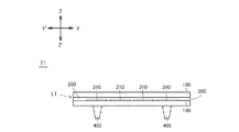
以下、本発明の実施例1に係るタッチ入力装置T1について図1A及び図1Bを参照しつつ説明する。なお、図1Aに示されるZ−Z’方向は、タッチ入力装置T1の樹脂積層体L1の厚み方向に相当し且つ特許請求の範囲の第1方向に相当する。図1A及び図1Bに示されるY−Y’方向は、タッチ入力装置T1の樹脂積層体L1の長手方向に相当する。Y−Y’方向はZ−Z’方向に直交している。図1Bに示されるX−X’方向は、タッチ入力装置T1の樹脂積層体L1の短手方向に相当する。X−X’方向は、Z−Z’方向及びY−Y’方向に直交している。 Hereinafter, a touch input device T1 according to a first embodiment of the invention will be described with reference to FIGS. 1A and 1B. Note that the Z-Z ′ direction shown in FIG. 1A corresponds to the thickness direction of the resin laminate L1 of the touch input device T1 and corresponds to the first direction of the claims. 1A and 1B corresponds to the longitudinal direction of the resin laminate L1 of the touch input device T1. The Y-Y ′ direction is orthogonal to the Z-Z ′ direction. The X-X ′ direction shown in FIG. 1B corresponds to the short direction of the resin laminate L1 of the touch input device T1. The X-X ′ direction is orthogonal to the Z-Z ′ direction and the Y-Y ′ direction.
タッチ入力装置T1は、樹脂積層体L1を備えている。樹脂積層体L1は、その全体が図1A及び図1Bに示されるようにY−Y’方向及びX−X’方向に延びるフラットな形状とすることが可能であるし、その全体がフラット以外の形状とすることが可能である。後者の場合、例えば、以下の1〜3)の何れかの形状とすることが可能である。1)樹脂積層体L1は湾曲している。例えば、樹脂積層体L1がY−Y’方向及び/又はX−X’方向に曲面状に湾曲している。2)樹脂積層体L1はフラットな部分と曲面状の部分とを有する。(例えば、樹脂積層体L1の中央部がフラットであり、樹脂積層体L1の端部がY−Y’方向及び/又はX−X’方向に円弧状に湾曲している。3)樹脂積層体L1は少なくとも一部に凸凹形状を有する。 The touch input device T1 includes a resin laminate L1. As shown in FIGS. 1A and 1B, the resin laminate L1 can have a flat shape extending in the YY ′ direction and the XX ′ direction, and the whole is not flat. It can be shaped. In the latter case, for example, any one of the following shapes 1 to 3) can be used. 1) The resin laminate L1 is curved. For example, the resin laminate L1 is curved in a curved shape in the Y-Y ′ direction and / or the X-X ′ direction. 2) The resin laminate L1 has a flat portion and a curved portion. (For example, the central portion of the resin laminate L1 is flat, and the end portion of the resin laminate L1 is curved in an arc shape in the YY ′ direction and / or the XX ′ direction. 3) Resin laminate L1 has an uneven shape at least partially.
樹脂積層体L1は、複数又は複数種の樹脂層100と、少なくとも一つの接着層200とを有している。タッチ入力装置T1の全ての樹脂層100は、押出成形されたシート又はフィルムである。タッチ入力装置T1は、押出成形された樹脂層100以外の樹脂層を備えていない。換言すると、タッチ入力装置T1の樹脂層としては、押出成形された樹脂層100のみを備えている。このように樹脂層100の各々は押出成形によって成形されているので、樹脂配向が一様であり、樹脂の密度分布が略均一であり、且つ樹脂積層体L1の形状起因以外の歪分布が殆どない。
The resin laminate L1 includes a plurality or types of
樹脂層100の各々は、ハードコート層、アンチグレア層、反射防止層、低反射層、電極基材層、保護層、アンチニュートン層、強度保持層、防汚層、位相差層(超高位相差層(SRF層)を含む。)、及び/又は耐指紋処理層等としての機能を付与するための処理(例えば、コーティング処理等)がされた構成とすることが可能である。例えば、図1Aでは、図示下側の樹脂層100は強度保持層及び電極基材層の機能付与の処理がされ、図示上側の樹脂層100は、ハードコート層、低反射層、耐指紋層及び保護層の機能付与の処理がされた構成とすることが可能である。超高位相差層の機能付与の処理がされた樹脂層100のリタデーション値は、3000〜30000nmであると良い。全ての樹脂層100のうちの少なくとも一つの樹脂層100に強度保持層の機能付与の処理がされている場合、強度保持層の機能付与の処理がされた樹脂層100は、強度保持層の機能付与の処理がされていない樹脂層100よりもZ−Z’方向の寸法が大きい構成とすることができる。例えば、強度保持層の機能付与の処理がされた樹脂層100のZ−Z’方向の寸法が1.5〜2.5mm程度であるのに対して、電極基材層の機能付与の処理がされた(強度保持層の機能付与の処理がされていない)樹脂層100のZ−Z’方向の寸法は、30〜300μm程度とすることが可能である。全ての樹脂層100に強度保持層の機能付与の処理がされていない場合、樹脂積層体L1全体で所定の強度が保たれる構成とすると良い。例えば、樹脂積層体L1全体の強度は、樹脂積層体L1に対して鋼球落下試験を行ったときに、樹脂積層体L1に大きな割れが生じない程度の強度とすると良い。この試験の衝撃吸収性は、10〜50Jである。
Each of the resin layers 100 includes a hard coat layer, an antiglare layer, an antireflection layer, a low reflection layer, an electrode substrate layer, a protective layer, an anti-Newton layer, a strength retention layer, an antifouling layer, a retardation layer (an ultrahigh retardation layer) (Including the SRF layer)) and / or a process for imparting a function as a fingerprint-resistant treatment layer or the like (for example, a coating treatment or the like). For example, in FIG. 1A, the
樹脂層100は、透光性を有していても良いし、不透明であっても良い。前者である場合、樹脂層100は透明であっても良い。樹脂層100は、可撓性を有していても良いし、有していなくても良い。樹脂層100の少なくとも一つには、加飾印刷が行われていても良い。
The
樹脂層100は、Z−Z’方向に積層されている。樹脂層100のうちZ−Z’方向で隣り合う樹脂層100が、接着層200によって接着されている。以下、樹脂層100のうち最もZ方向に位置する樹脂層100を最表層とも称し、樹脂層100のうち最もZ’方向に位置する樹脂層100を最深層とも称する。なお、図1A及び図1Bでは、樹脂層100は、二つであるが、三つ以上であっても良い。
The
樹脂層100は、以下の1)〜5)の少なくとも一つの構成を有していても良い。1)樹脂層100が非晶性樹脂又は結晶性樹脂で構成されている。非晶性樹脂としては、例えば、ポリカーボネート(PC)、ポリスチレン(PS)、シクロオレフィンコポリマー(COC)、シクロオレフィンポリマー(COP)又はポリメチルメタクリレート(PMMA)等である。非晶性樹脂は、分子配列に規則性のない状態で固化するため、強い配向を持たない。非晶性樹脂は、押圧成形の成形性が良く、成形時の熱収縮が小さい。非晶性樹脂は、透明性が高い。結晶性樹脂としては、例えば、ポリエチレンテレフタレート(PET)やポリプロピレン(PP)等である。2)樹脂層100は、Y−Y’方向及びX−X’方向に二軸延伸された構成とすることが可能である。この場合、全ての樹脂層100の流れ方向(MD方向)が一致し且つ全ての樹脂層100の直角方向(TD方向)が一致している。直角方向は、流れ方向に対して直角である。図1A及び図1Bでは、流れ方向はY−Y’方向に相当し、直角方向はX−X’方向に相当している。
The
3)樹脂層100の主材料は、同種の高分子材料である。4)各樹脂層100の線膨張係数が、4〜15×10−5cm/cm・℃である。例えば、樹脂層100がポリカーボネートやシクロオレフィンポリマーである場合、その線膨張係数は約6.5×10−5cm/cm・℃となる。5)タッチ入力装置T1が使用される環境温度において、樹脂層100が熱膨張により延びるとき又は熱収縮により縮むときに、隣り合う樹脂層100に相対的に生じる全長の差異が、隣り合う樹脂層100間の接着層200のZ−Z’方向の寸法(厚み寸法)の20%以下となっている。なお、タッチ入力装置T1が車載用である場合、環境温度は−40℃〜85℃であり、タッチ入力装置T1が民生用である場合、環境温度は−10℃〜60℃である。なお、環境温度は、適宜設定でき、前述の例に限定されない。5)の場合、以下の5−1)〜5−4)の少なくとも一つによって実現される。5−1)樹脂層100の材料については、線膨張係数及び熱収縮が近いものを選定する。5−2)接着層200のZ−Z’方向の寸法(厚み寸法)を大きくする。5−3)樹脂層100が無延伸フィルムで構成されている。この場合、樹脂層100は二軸延伸された構成とすることができないが、次の構成とすることが可能である。全ての樹脂層100の流れ方向(MD方向)が一致し且つ全ての樹脂層100の直角方向(TD方向)が一致している。5−4)樹脂層100の押出成形時の条件をコントロールする。
3) The main material of the
少なくとも一つの接着層200は、上記した通り隣り合う樹脂層100を接着している。接着層200は、例えば、ウェットラミネート接着剤、ドライラミネート接着剤、又はホットメルト接着剤等とすることが可能である。ドライラミネート接着剤としては、例えば、OCA(Optical Clear Adhesive;登録商標)を用いることができる。接着層200のガラス転移温度(Tg)は、上記環境温度以上とすることが可能である。なお、タッチ入力装置T1が車載用である場合、接着層200のガラス転移温度は85℃以上であり、タッチ入力装置T1が民生用である場合、接着層200のガラス転移温度は60℃以上である。又は、接着層200が、上記環境温度の範囲内で、粘弾性を有する構成とすることが可能である。
At least one
タッチ入力装置T1は、表面型静電容量(Surface Capacitive)方式及び投影型静電容量(Projected Capacitive)方式の何れか一方のタッチパネルとすることが可能である。 The touch input device T1 can be a touch panel of any one of a surface capacitive type and a projected capacitive type.
タッチ入力装置T1は、少なくとも一つの電極層300を更に備えている。少なくとも一つの電極層300は、上記した何れかの静電容量方式により検出対象(例えば、指又はタッチペンの導体)の最表層に対する接近を検出可能な電極層であって、樹脂層100のうちの少なくとも一つの樹脂層100上に設けられており且つ接着層200によって接着された隣り合う二つの樹脂層100間に配置されている。
The touch input device T1 further includes at least one
タッチ入力装置T1が表面型静電容量方式のタッチパネルである場合、電極層300は一つとすることが可能である。電極層300は一つの電極310を有している。この場合、電極310は、透明導電膜である。前記透明導電膜は、例えば、ITO(酸化インジウム+酸化錫)又はATO( アンチモン酸化スズ)等で構成されており且つ検出対象の最表層に対する接近に応じて、当該電極310の四つの角部の電界値が変化する構成となっている。
When the touch input device T1 is a surface capacitive touch panel, the number of
タッチ入力装置T1が投影型静電容量方式のタッチパネルである場合、電極層300は一つとすることが可能である。電極層300は複数の電極310を有している。この場合、電極310は、透明導電膜又は導体である。前記透明導電膜は、例えば、ITO(酸化インジウム+酸化錫)、CNT(カーボンナノチューブ)、IZO(酸化インジウム+酸化亜鉛)、AZO(AIドープ酸化亜鉛)又は導電性高分子(PEDOT又はPSS)等で構成されている。前記導体は、例えば、感光性銀、銀ナノインク、銀ナノワイヤ、蒸着銅、圧延銅又は銅ナノインク等である。電極310が樹脂層100のうちの少なくとも一つの樹脂層100上に互いに間隔をあけて設けられている。なお、タッチ入力装置T1が投影型静電容量方式である場合、自己キャパシタンス方式及び相互キャパシタンス方式の何れか一方のタッチパネルとすることが可能である。
When the touch input device T1 is a projected capacitive touch panel, the number of
タッチ入力装置T1が自己キャパシタンス方式のタッチパネルである場合、電極310は、検出対象の最表層に対する接近に応じて、当該電極310と検出対象との間に発生する静電容量が変化し、静電容量の変化に応じて電極310の電気信号(電圧又は電流)が変化する構成となっている。なお、タッチ入力装置T1は、自己キャパシタンス方式のタッチスイッチとすることが可能である。この場合、電極層300は少なくとも一つ電極310を有していれば良い。
When the touch input device T1 is a self-capacitance type touch panel, the capacitance of the
タッチ入力装置T1が相互キャパシタンス方式のタッチパネルである場合、電極310のうち隣り合う電極310のうち一方が駆動電極(ドライブ電極)であり、他方が検出電極(センサ電極)となる。例えば、図1Bでは、電極層300は、図示左から右へ第1列の電極310、第2列の電極310、第3列の電極310、及び第4列の電極310を有しており、第1列の電極310及び第3列の電極310を駆動電極、第2列の電極310及び第4列の電極310を検出電極とすることが可能である。又は、第1列の電極310及び第3列の電極310を検出電極、第2列の電極310及び第4列の電極310を駆動電極とすることも可能である。隣り合う駆動電極と検出電極とが各々静電結合されている。検出対象の接近に応じて、隣り合う駆動電極と検出電極との間に発生する静電容量が変化し、静電容量の変化に応じて、検出電極の電気信号(電圧又は電流)が変化する構成となっている。なお、タッチ入力装置T1が相互キャパシタンス方式のタッチスイッチとすることが可能である。この場合、電極層300は、少なくとも隣り合う二つ電極310を有していれば良い。
When the touch input device T1 is a mutual capacitance touch panel, one of the
タッチ入力装置T1は、図示しない検出部を更に備えていても良い。タッチ入力装置T1が表面静電容量方式のタッチパネルである場合、検出部は、電極310の四角の電界値の変化を検出し、最表層に対する検出対象のタッチ位置を検出可能な検出回路となっている。タッチ入力装置T1が、自己キャパシタンス方式のタッチパネル、又は自己キャパシタンス方式のタッチスイッチ、検出部は、電極310の電気信号(電圧又は電流)の変化を検出し、最表層に対する検出対象のタッチ位置を検出可能な検出回路となっている。タッチ入力装置T1が、相互キャパシタンス方式のタッチパネル又は相互キャパシタンス方式のタッチスイッチである場合、検出部は、検出電極の電気信号(電圧又は電流)の変化を検出し、最表層に対する検出対象のタッチ位置を検出可能な検出回路となっている。なお、タッチ入力装置T1が搭載される電子機器の制御部が検出部を備えている場合には、タッチ入力装置T1の検出部は省略可能である。
The touch input device T1 may further include a detection unit (not shown). When the touch input device T1 is a surface capacitive touch panel, the detection unit detects a change in the square electric field value of the
タッチ入力装置T1は、複数のリブ400を更に備えていても良い。リブ400は、樹脂積層体L1の最深層上に固着されている。リブ400は、例えば、最深層と同種又は同一の樹脂で構成されていても良いし、同種又は同一の樹脂を含むポリマーアロイで構成されていても良い。このような素材でリブ400が構成されている場合、リブ400と最深層との密着性及び相溶性が高くなるので、両者が強固に固着される。リブ400はこれ以外の素材で構成されていても良い。リブ400は、前記電子機器のフレームや前記電子機器内の表示装置等に取り付け可能である。なお、リブ400は省略可能である。
The touch input device T1 may further include a plurality of
以下、上記したタッチ入力装置T1の製造方法について詳しく説明する。まず、複数又は複数種の樹脂層100を用意する。具体的には、押出成形機を用いて複数又は複数種の溶融樹脂をシート状又はフィルム状に押出成形する。押出成形された溶融樹脂が複数又は複数種の樹脂層100となる。溶融樹脂は、結晶性樹脂及び非晶性樹脂の何れであっても良い。押出成形時に、溶融樹脂がY−Y’方向及びX−X’方向に二軸延伸されていても良い。溶融樹脂の主材料は、同種の高分子材料であっても良い。溶融樹脂の上記線膨張係数としても良い。上記環境温度において、樹脂層100が熱膨張により延びるとき又は熱収縮により縮むときに、隣り合う樹脂層100に相対的に生じる全長の差異が、隣り合う樹脂層100間の接着層200のZ−Z’方向の寸法(厚み寸法)の20%以下となるように、樹脂層100の材料、樹脂層100の材料の粘度、及び/又は樹脂層100の押出成形時の条件等が設定されていても良い。その後、押出成形された樹脂層100に対して、ハードコート層、アンチグレア層、反射防止層、低反射層、電極基材層、保護層、アンチニュートン層、強度保持層、防汚層、位相差層(超高位相差層(SRF層)を含む。)、及び/又は耐指紋処理層の機能を付与するための各種処理(例えば、コーティング処理等)が行われていても良い。このようにして樹脂層100が用意される。
Hereinafter, a method for manufacturing the touch input device T1 will be described in detail. First, a plurality or types of
その後、樹脂層100の少なくとも一つの樹脂層100上に電極層300の電極310を形成する。その後、樹脂層100を接着層200で貼り合わせ、樹脂層100がZ−Z’方向において積層される。このとき、電極層300がZ−Z’方向において隣り合う樹脂層100間に配置される。この樹脂層100の積層は、各樹脂層100の流れ方向が一致し且つ各樹脂層100の直角方向が一致するように、樹脂層100を積層しても良い。このようにして全体がフラットな樹脂積層体L1が得られる。
Thereafter, the
樹脂積層体L1の全体が上記したフラット以外の形状である場合、樹脂積層体L1を加熱軟化させた後、図示しない型を用いて樹脂積層体L1を真空成形、圧空成形又はプレス成形する。これにより、樹脂積層体L1が型の形に応じて変形する(例えば、樹脂積層体L1の少なくとも一部がY−Y’方向及び/又はX−X’方向に曲面状に湾曲したり、凹凸が生じたりする)。このようにして樹脂積層体L1に形状付与が行われる。 When the entire resin laminate L1 has a shape other than the flat shape described above, the resin laminate L1 is heat-softened, and then the resin laminate L1 is vacuum-formed, pressure-formed, or press-molded using a mold (not shown). Thereby, the resin laminate L1 is deformed according to the shape of the mold (for example, at least a part of the resin laminate L1 is curved in a curved shape in the YY ′ direction and / or the XX ′ direction, or uneven) May occur). In this way, shape imparting is performed on the resin laminate L1.
タッチ入力装置T1がリブ400を備えている場合、リブ400を接着剤や両面テープ等でフラットな樹脂積層体L1又は形状付与された樹脂積層体L1の最深層に固着しても良い。又は、フラットな樹脂積層体L1又は形状付与された樹脂積層体L1を図示しない金型内に入れて、樹脂積層体L1の最深層上にリブ400が成形されるようにアウトサート成形を行っても良い。以上のようにタッチ入力装置T1が製造される。
When the touch input device T1 includes the
以上のようなタッチ入力装置T1は以下の技術的特徴を有している。第1に、隣り合う樹脂層100の一方が他方から剥離する可能性が抑制される。その理由は以下の通りである。タッチ入力装置T1の全ての樹脂層100が押出成形によって作成されている。この樹脂層100がZ−Z’方向において積層されるときに、隣り合う樹脂層100が接着層200によって接着されている。このため、積層後、樹脂層100が成形収縮しないので、この成形収縮により樹脂層100に応力が生じない。また、樹脂層100が非晶性樹脂で構成されている場合、樹脂層100の膨張及び/又は収縮が抑制される。また、一般的に、押出成形された樹脂層100の熱収縮は、流れ方向において相違し、直角方向において略相違しない(すなわち、実質的にゼロ近辺である)ことが多い。よって、樹脂層100の流れ方向が一致し、且つ樹脂層100の直角方向が一致していることで、樹脂層100の熱収縮の相違によって、隣り合う樹脂層100が剥離する可能性を低減することができる。また、樹脂層100の主材料は同種の高分子材料である場合、樹脂層100の膨張量及び収縮量が近くなる。また、樹脂層100の線膨張係数が上記の通りである場合、樹脂層100の膨張量及び収縮量が近くなる。また、上記環境温度下で、樹脂層100が熱膨張により延びるとき又は熱収縮により縮むときに、隣り合う樹脂層100に相対的に生じる全長の差異が、隣り合う樹脂層100間の接着層200のZ−Z’方向の寸法(厚み寸法)の20%以下である場合、タッチ入力装置T1が環境温度下で使用され、隣り合う樹脂層100が熱膨張及び/又は熱収縮したとしても、接着層200が、熱膨張及び/又は熱収縮した樹脂層100に追従できる。また、接着層200のガラス転移温度(Tg)が上記環境温度以上である場合、接着層200が環境温度下で固化状態となるので、接着層200によって隣り合う樹脂層100を強固に接着される。又は、接着層200が環境温度の範囲内で、粘弾性を有する場合、接着層200が環境温度下で軟化状態となるので、接着層200によって隣り合う樹脂層100が樹脂層100に生じる剥離応力に応じて追従する。
The touch input device T1 as described above has the following technical features. First, the possibility that one of the
第2に、タッチ入力装置T1の樹脂積層体L1の樹脂層100は、射出成形されないので、射出成形用の金型と樹脂層100との間に異物が混入することがない。第3に、タッチ入力装置T1の樹脂積層体L1の歪みが小さくなり、且つ樹脂積層体L1のリタデーション値が小さくなる。換言すると、各樹脂層100において、複屈折の偏在やムラが少なくなる。よって、タッチ入力装置T1が偏光板(偏光サングラス等)を介して視認される場合であっても、樹脂積層体L1に虹ムラが生じ難くなる。
Second, since the
特に、タッチ入力装置T1が、自動車のインスツルメントパネル(instrument panel)等の湿熱環境下(上記環境温度下)で使用される場合、樹脂積層体L1全体がフラット以外の形状である場合、樹脂積層体L1が大面積(200〜20000cm2)である場合、上記した技術的特徴が顕著になる。 In particular, when the touch input device T1 is used in a humid heat environment (under the above environmental temperature) such as an instrument panel of an automobile, the resin laminate L1 has a shape other than a flat shape. When the laminated body L1 has a large area (200 to 20000 cm2), the above-described technical features become remarkable.
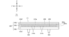
以下、本発明の実施例2に係るタッチ入力装置T2について図2A及び図2Bを参照しつつ説明する。タッチ入力装置T2は、相互キャパシタンス方式のタッチパネルであって、次の相違点以外、タッチ入力装置T1と同様の構成となっている。相違点1)タッチ入力装置T2は、電極層300に代えて、第1電極層300a及び第2電極層300bを備えている。相違点2)樹脂積層体L2の複数又は複数種の樹脂層100’が、第1樹脂層及び第2樹脂層を含んでいる。相違点3)樹脂積層体L2の接着層200が複数である。以下、これらの相違点についてのみ詳しく説明し、タッチ入力装置T2の説明のうち、タッチ入力装置T1と重複するものについて省略する。なお、図2Aに示されるZ−Z’方向は、タッチ入力装置T2の樹脂積層体L2の厚み方向に相当し且つ特許請求の範囲の第1方向に相当する。図2A及び図2Bに示されるY−Y’方向は、タッチ入力装置T2の樹脂積層体L2の長手方向に相当する。Y−Y’方向はZ−Z’方向に直交している。図2Bに示されるX−X’方向は、タッチ入力装置T2の樹脂積層体L2の短手方向に相当する。X−X’方向は、Z−Z’方向及びY−Y’方向に直交している。
Hereinafter, a touch input device T2 according to a second embodiment of the invention will be described with reference to FIGS. 2A and 2B. The touch input device T2 is a mutual capacitance touch panel, and has the same configuration as the touch input device T1 except for the following differences. Difference 1) The touch input device T2 includes a
樹脂層100’は、実施例1の樹脂層100と同様の構成とすることが可能である。樹脂層100’は、樹脂層100a、樹脂層100b(第1樹脂層)、樹脂層100c(第2樹脂層)及び樹脂層100dを含んでいる。樹脂層100’は、樹脂層100a〜100d以外の樹脂層を更に含んでいても良い。樹脂層100’は、Z−Z’方向に積層されている。隣り合う樹脂層100’は、接着層200によって接着されている。樹脂層100a、樹脂層100b、樹脂層100c及び樹脂層100dは、この順でZ−Z’方向に積層されている。隣り合う樹脂層100aと樹脂層100bが接着層200によって接着されている。隣り合う樹脂層100bと樹脂層100cが別の接着層200によって接着されている。隣り合う樹脂層100cと樹脂層100dが更に別の接着層200によって接着されている。図2A及び図2Bでは、樹脂層100aが最表層であり、樹脂層100dが最深層である。
The
樹脂層100aは、保護層の機能付与の処理がされた構成とすることが可能である。この樹脂層100aは、ハードコート層、アンチグレア層、反射防止層、低反射層、アンチニュートン層、強度保持層、防汚層、位相差層(超高位相差層(SRF層)を含む。)、及び/又は耐指紋処理層等の機能付与の処理が更にされた構成とすることが可能である。樹脂層100aには、加飾印刷が行われていても良い。
The
樹脂層100b及び樹脂層100cは、電極基材層の機能付与の処理がされた構成とすることが可能である。樹脂層100b及び樹脂層100cは、ハードコート層、アンチグレア層、反射防止層、低反射層、アンチニュートン層、防汚層、位相差層(超高位相差層(SRF層)を含む。)、及び/又は耐指紋処理層等の機能付与の処理が更にされた構成とすることが可能である。
The
樹脂層100dは、強度保持層の機能付与の処理がされた構成とすることが可能である。樹脂層100dは、ハードコート層、アンチグレア層、反射防止層、低反射層、保護層、アンチニュートン層、防汚層、位相差層(超高位相差層(SRF層)を含む。)、及び/又は耐指紋処理層等の機能付与の処理が更にされた構成とすることが可能である。
The
第1電極層300aは、複数の第1電極310aを有している。第1電極310aは、Y−Y’方向に延びた透明導電膜又は導体であって、樹脂層100b上にX−X’方向に間隔をあけて設けられている。この第1電極310aが隣り合う樹脂層100aと樹脂層100bの間に配置されている。第2電極層300bは、複数の第2電極310bを有している。第2電極310bは、X−X’方向に延びた透明導電膜又は導体であって、樹脂層100c上にY−Y’方向に間隔をあけて設けられている。第2電極310bが隣り合う樹脂層100bと樹脂層100cの間に配置されている。第1電極310a及び第2電極310bはZ−Z’方向の異なる高さ位置で互いに交差している。第1電極310a及び第2電極310bのうちの何れか一方が駆動電極(ドライブ電極)であり、他方が検出電極(センサ電極)である。前記透明導電膜は、ITO(酸化インジウム+酸化錫)、CNT(カーボンナノチューブ)、IZO(酸化インジウム+酸化亜鉛)、AZO(AIドープ酸化亜鉛)又は導電性高分子(PEDOT又はPSS)等で構成されている。前記導体は、感光性銀やグラフオフセット等で作製された線幅15μm以下の金属(例えば、Ag、Cu)、銀ナノインク、銀ナノワイヤ、メタルワイヤー、蒸着銅、圧延銅又は銅ナノインク等で構成された導体である。
The
上記したタッチ入力装置T2の製造方法は、次の通り製造される。タッチ入力装置T1の製造方法の樹脂層100と同様に、複数又は複数種の樹脂層100’(樹脂層100a〜100d)を用意する。
The manufacturing method of the touch input device T2 described above is manufactured as follows. Similar to the
その後、樹脂層100b上に第1電極層300aの第1電極310aをX−X’方向に間隔をあけて形成する。樹脂層100c上に、第2電極層300bの第2電極310bをY−Y’方向に間隔をあけて形成する。
Thereafter, the
その後、第1電極層300aが樹脂層100aと樹脂層100bの間に配置されるように樹脂層100aと樹脂層100bを接着層200で貼り合わせ、第2電極層300bが樹脂層100bと樹脂層100cの間に配置されるように樹脂層100bと樹脂層100cを接着層200で貼り合わせ、且つ樹脂層100cと樹脂層100dを接着層200で貼り合わせる。これにより、樹脂層100a〜100dがZ−Z’方向において積層される。この樹脂層100a〜100dの積層では、樹脂層100a〜100dの流れ方向が一致し且つ樹脂層100a〜100dの直角方向が一致するように、樹脂層100a〜100dを積層しても良い。このようにして全体がフラットな樹脂積層体L2が得られる。
Thereafter, the
樹脂積層体L2についても、タッチ入力装置T1の製造方法と同様に形状付与を行うことが可能である。タッチ入力装置T2がリブ400を備えている場合、リブ400をタッチ入力装置T1の製造方法と同様に、樹脂積層体L2に固着(アウトサート成形を含む)すると良い。以上のようにタッチ入力装置T2が製造される。
The resin laminate L2 can also be given a shape in the same manner as the manufacturing method of the touch input device T1. When the touch input device T2 includes the
以上のようなタッチ入力装置T2は、タッチ入力装置T1と同様の技術的特徴を有している。 The touch input device T2 as described above has the same technical features as the touch input device T1.
以下、本発明の実施例3に係るタッチ入力装置T3について図3を参照しつつ説明する。タッチ入力装置T3は、相互キャパシタンス方式のタッチパネルであって、次の相違点以外、タッチ入力装置T2と同様の構成となっている。相違点1)第1電極層300aが第1樹脂層の第1面101b’上に設けられ且つ第2電極層300bが第1樹脂層の第2面102b’上に設けられている。相違点2)樹脂積層体L2の複数又は複数種の樹脂層100’’が、第1樹脂層を含み、第2樹脂層を含んでいない。以下、これらの相違点についてのみ詳しく説明し、タッチ入力装置T3の説明のうち、タッチ入力装置T2と重複するものについて省略する。なお、図3には、Z−Z’方向及びY−Y’方向が、タッチ入力装置T2と同様に示されている。X−X’方向については、図2Bを借りて参照する。
Hereinafter, a touch input device T3 according to a third embodiment of the invention will be described with reference to FIG. The touch input device T3 is a mutual capacitance touch panel, and has the same configuration as the touch input device T2 except for the following differences. Difference 1) The
樹脂層100’’は、実施例1の樹脂層100と同様の構成とすることが可能である。樹脂層100’’は、樹脂層100a’、樹脂層100b’(第1樹脂層)、及び樹脂層100c’を含んでいる。樹脂層100’’は、樹脂層100a’〜100c’以外の樹脂層を更に含んでいても良い。樹脂層100’’は、Z−Z’方向に積層されている。隣り合う樹脂層100’’は、接着層200によって接着されている。樹脂層100a’、樹脂層100b’、及び樹脂層100c’は、この順でZ−Z’方向に積層されている。隣り合う樹脂層100a’と樹脂層100b’が接着層200によって接着されている。隣り合う樹脂層100b’と樹脂層100c’が別の接着層200によって接着されている。図3では、樹脂層100a’が最表層であり、樹脂層100c’が最深層である。
The
樹脂層100a’は、タッチ入力装置T2の樹脂層100aと同様の構成とすることが可能である。樹脂層100c’は、タッチ入力装置T2の樹脂層100dと同様の構成とすることが可能である。
The
樹脂層100b’は、次の点を除き、タッチ入力装置T2の樹脂層100bと同様の構成とすることが可能である。樹脂層100b’は、Z’方向の第1面101b’と、Z方向の第2面102b’とを有している。
The
タッチ入力装置T3の第1電極層300aは、第1電極310aが樹脂層100b’の第1面101b’上に設けられている以外、タッチ入力装置T2の第1電極層300aと同様の構成である。タッチ入力装置T3の第2電極層300bは、第2電極310bが樹脂層100b’の第2面102b’上に設けられている以外、タッチ入力装置T2の第2電極層300bと同様の構成である。
The
上記したタッチ入力装置T3の製造方法は、次の通り製造される。タッチ入力装置T1の製造方法の樹脂層100と同様に、複数又は複数種の樹脂層100’’(樹脂層100a’〜100c’)を用意する。
The manufacturing method of the touch input device T3 described above is manufactured as follows. Similar to the
その後、樹脂層100b’の第1面101b’上に第1電極層300aの第1電極310aをX−X’方向に間隔をあけて形成する。樹脂層100b’の第2面102b’上に、第2電極層300bの第2電極310bをY−Y’方向に間隔をあけて形成する。
Thereafter, the
その後、第1電極層300aが樹脂層100a’と樹脂層100b’の間に配置されるように、樹脂層100a’と樹脂層100b’を接着層200で貼り合わせ、且つ第2電極層300bが樹脂層100b’と樹脂層100c’の間に配置されるように、樹脂層100b’と樹脂層100c’を接着層200で貼り合わせる。これにより、樹脂層100a’〜100c’がZ−Z’方向において積層される。この樹脂層100a’〜100c’の積層では、樹脂層100a’〜100c’の流れ方向が一致し且つ樹脂層100a’〜100c’の直角方向が一致するように、樹脂層100a’〜100c’を積層しても良い。このようにして全体がフラットな樹脂積層体L3が得られる。
Thereafter, the
樹脂積層体L3についても、タッチ入力装置T1の製造方法と同様に形状付与を行うことが可能である。タッチ入力装置T3がリブ400を備えている場合、リブ400をタッチ入力装置T1の製造方法と同様に、樹脂積層体L3に固着(アウトサート成形を含む)すると良い。以上のようにタッチ入力装置T3が製造される。
The resin laminate L3 can also be given a shape in the same manner as the manufacturing method of the touch input device T1. When the touch input device T3 includes the
以上のようなタッチ入力装置T3は、タッチ入力装置T1と同様の技術的特徴を有している。 The touch input device T3 as described above has the same technical features as the touch input device T1.
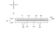
以下、本発明の実施例4に係るタッチ入力装置T4について図4を参照しつつ説明する。タッチ入力装置T4は、相互キャパシタンス方式のタッチパネルであって、次の相違点以外、タッチ入力装置T2と同様の構成となっている。相違点1)タッチ入力装置T4が絶縁層500を更に備えている。相違点2)第1電極層300a、絶縁層500及び第2電極層300bが第1樹脂層上にZ−Z’方向において積層されている。相違点3)樹脂積層体L3の複数又は複数種の樹脂層100’’’が、第1樹脂層を含んでおり、第2樹脂層を含んでいない。以下、これらの相違点についてのみ詳しく説明し、タッチ入力装置T4の説明のうち、タッチ入力装置T2と重複するものについて省略する。なお、図4には、Z−Z’方向及びY−Y’方向が、タッチ入力装置T2と同様に示されている。X−X’方向については、図2Bを借りて参照する。
Hereinafter, a touch input device T4 according to a fourth embodiment of the invention will be described with reference to FIG. The touch input device T4 is a mutual capacitance touch panel, and has the same configuration as the touch input device T2 except for the following differences. Difference 1) The touch input device T4 further includes an insulating
樹脂層100’’’は、実施例1の樹脂層100と同様の構成とすることが可能である。樹脂層100’’’は、樹脂層100a’’及び樹脂層100b’(第1樹脂層)を含んでいる。樹脂層100’’’は、樹脂層100a’’及び樹脂層100b’以外の樹脂層を更に含んでいても良い。樹脂層100’’’は、Z−Z’方向に積層されている。隣り合う樹脂層100’’’は、接着層200によって接着されている。樹脂層100a’’及び樹脂層100b’’は、この順でZ−Z’方向に積層されている。隣り合う樹脂層100a’’と樹脂層100b’’が接着層200によって接着されている。図4では、樹脂層100a’’が最表層であり、樹脂層100b’’が最深層である。
The
樹脂層100a’’は、タッチ入力装置T2の樹脂層100aと同様の構成とすることが可能である。樹脂層100b’’は、電極基材層及び強度保持層の機能付与の処理がされた構成とすることが可能である。樹脂層100b’’は、ハードコート層、アンチグレア層、反射防止層、低反射層、保護層、アンチニュートン層、防汚層、位相差層(超高位相差層(SRF層)を含む。)、及び/又は耐指紋処理層等の機能付与の処理が更にされた構成とすることが可能である。
The
タッチ入力装置T4の第1電極層300aは、第1電極310aが樹脂層100b’’上に設けられている以外、タッチ入力装置T2の第1電極層300aと同様の構成である。絶縁層500は、第1電極層300aを覆うように第1電極層300a上に設けられている。第2電極層300bは、第2電極310bが絶縁層500上に設けられている以外、実施例2の第2電極層300bと同様の構成である。第1電極層300a、絶縁層500及び第2電極層300bが隣り合う樹脂層100a’’と樹脂層100b’’との間に配置されている。
The
絶縁層500は、透光性を有していても良いし、不透明であっても良い。前者の場合、絶縁層500は、透明であっても良い。樹脂層100は、可撓性を有していても良いし、有していなくても良い。
The insulating
上記したタッチ入力装置T4の製造方法は、次の通り製造される。タッチ入力装置T1の製造方法の樹脂層100と同様に、複数又は複数種の樹脂層100’’’(樹脂層100a’’及び樹脂層100b’’)を用意する。
The manufacturing method of the touch input device T4 described above is manufactured as follows. Similar to the
その後、樹脂層100b’’上に第1電極層300aの第1電極310aをX−X’方向に間隔をあけて形成する。第1電極層300aを覆うように、第1電極層300a上に絶縁層500を形成する。絶縁層500上に、第2電極層300bの第2電極310bをY−Y’方向に間隔をあけて形成する。
Thereafter, the
その後、第1電極層300a、絶縁層500及び第2電極層300bが樹脂層100a’’と樹脂層100b’’の間に配置されるように、樹脂層100a’’と樹脂層100b’’を接着層200で貼り合わせる。これにより、樹脂層100a’’及び樹脂層100b’’がZ−Z’方向において積層される。この樹脂層100a’’及び樹脂層100b’’の積層では、樹脂層100a’’及び樹脂層100b’’の流れ方向が一致し、且つ樹脂層100a’’及び樹脂層100b’’の直角方向が各々一致するように、樹脂層100a’’及び樹脂層100b’’を積層しても良い。このようにして全体がフラットな樹脂積層体L4が得られる。
Thereafter, the
樹脂積層体L4についても、タッチ入力装置T1の製造方法と同様に形状付与を行うことが可能である。タッチ入力装置T4がリブ400を備えている場合、リブ400をタッチ入力装置T1の製造方法と同様に、樹脂積層体L4に固着(アウトサート成形を含む)すると良い。以上のようにタッチ入力装置T4が製造される。
The resin laminate L4 can also be given a shape in the same manner as the manufacturing method of the touch input device T1. When the touch input device T4 includes the
以上のようなタッチ入力装置T4は、タッチ入力装置T1と同様の技術的特徴を有している。 The touch input device T4 as described above has the same technical features as the touch input device T1.
なお、上記したタッチ入力装置は、上記実施例に限定されるものではなく、特許請求の範囲の記載範囲において任意に設計変更することが可能である。以下、詳しく述べる。 The touch input device described above is not limited to the above-described embodiment, and can be arbitrarily changed in design within the scope of the claims. Details will be described below.
本発明の電極層は省略可能である。この場合、本発明の樹脂積層体は、タッチ入力装置の樹脂積層体に限定されず、他の用途に使用可能である。例えば、本発明の樹脂積層体の樹脂層間に何も設けられていない構成とすることが可能であるし、樹脂積層体の樹脂層間に、電極層以外のシート状のセンサ、表示装置(例えば、有機ELディスプレイ等)、照明装置、加飾、投影スクリーン、ヒータ、電磁シールド、ミラー、圧電素子、緩衝材、通信装置(例えば、アンテナ等)、発電装置(例えば、太陽電池等)、殺菌装置(例えば、UV発光装置、熱源等)、又は電子回路等が配置される構成とすることが可能である。このように本発明は、自動車のインスツルメントパネル以外にも適応可能である。 The electrode layer of the present invention can be omitted. In this case, the resin laminate of the present invention is not limited to the resin laminate of the touch input device, and can be used for other purposes. For example, it is possible to have a configuration in which nothing is provided between the resin layers of the resin laminate of the present invention, and between the resin layers of the resin laminate, a sheet-like sensor other than the electrode layer, a display device (for example, Organic EL display, etc.), lighting device, decoration, projection screen, heater, electromagnetic shield, mirror, piezoelectric element, buffer material, communication device (eg, antenna), power generation device (eg, solar cell), sterilizer ( For example, a UV light emitting device, a heat source, or the like) or an electronic circuit or the like can be arranged. Thus, the present invention can be applied to other than the instrument panel of the automobile.
なお、上記実施例及び設計変形例における本発明の各構成要素を構成する素材、形状、寸法、数及び配置等はその一例を説明したものであって、同様の機能を実現し得る限り任意に設計変更することが可能である。上記した実施例及び設計変更例は、互いに矛盾しない限り、相互に組み合わせることが可能である。 Note that the materials, shapes, dimensions, numbers, arrangements, and the like constituting each component of the present invention in the above-described embodiments and design modifications are examples, and are arbitrary as long as similar functions can be realized. It is possible to change the design. The above-described embodiments and design modification examples can be combined with each other as long as they do not contradict each other.
T1:タッチ入力装置
L1:樹脂積層体
100:樹脂層
200:接着層
300 :電極層
310:電極
400:リブ
T2:タッチ入力装置
L2:樹脂積層体
100’:樹脂層
100a〜100d:樹脂層
200:接着層
300a:第1電極層
310a:第1電極
300b:第2電極層
310b:第2電極
400:リブ
T3:タッチ入力装置
L3:樹脂積層体
100’’:樹脂層
100a’〜100c’:樹脂層
101b’:第1面
102b’:第2面
200:接着層
300a:第1電極層
310a:第1電極
300b:第2電極層
310b:第2電極
400:リブ
T4:タッチ入力装置
L4:樹脂積層体
100’’’:樹脂層
100a’’〜100b’’:樹脂層
200:接着層
300a:第1電極層
310a:第1電極
300b:第2電極層
310b:第2電極
400:リブ
500:絶縁層
T1: Touch input device L1: Resin laminate 100: Resin layer 200: Adhesive layer 300: Electrode layer 310: Electrode 400: Rib T2: Touch input device L2:
Claims (14)
前記樹脂層のうち前記第1方向で隣り合う樹脂層を接着させる接着層とを備えた樹脂積層体であって、
前記樹脂積層体は、前記樹脂層の全てが押出成形された構成であり、押出成形された前記樹脂層以外の樹脂層を備えていない樹脂積層体。 A plurality or types of resin layers laminated in the first direction;
A resin laminate including an adhesive layer for adhering adjacent resin layers in the first direction among the resin layers,
The resin laminate has a configuration in which all of the resin layer is extruded and does not include a resin layer other than the extruded resin layer.
前記樹脂層は、非晶性樹脂で構成されている樹脂積層体。 The resin laminate according to claim 1,
The resin layer is a resin laminate composed of an amorphous resin.
前記樹脂層の流れ方向が一致し且つ前記樹脂層の直角方向が一致しており、
前記直角方向は前記流れ方向に対して直角である樹脂積層体。 In the resin laminate according to claim 1 or 2,
The flow direction of the resin layer matches and the perpendicular direction of the resin layer matches,
The resin laminate in which the perpendicular direction is perpendicular to the flow direction.
前記樹脂層の主材料は、同種の高分子材料である樹脂積層体。 In the resin laminated body in any one of Claims 1-3,
The main material of the resin layer is a resin laminate that is the same kind of polymer material.
前記樹脂層の線膨張係数が、4〜15×10−5cm/cm・℃である樹脂積層体。 In the resin laminated body in any one of Claims 1-4,
The resin laminated body whose linear expansion coefficient of the said resin layer is 4-15 * 10 < -5 > cm / cm * degreeC.
−40℃〜85℃において、前記樹脂層が熱膨張により延びるとき又は熱収縮により縮むときに、前記隣り合う樹脂層に相対的に生じる全長の差異が、前記隣り合う樹脂層の前記接着層の厚み寸法の20%以下である樹脂積層体。 In the resin laminated body in any one of Claims 1-5,
When the resin layer extends due to thermal expansion or contracts due to thermal contraction at −40 ° C. to 85 ° C., the difference in the overall length that occurs relatively in the adjacent resin layers is the difference between the adhesive layers of the adjacent resin layers. A resin laminate that is 20% or less of the thickness dimension.
前記接着層のガラス転移温度は、60℃以上である樹脂積層体。 In the resin laminated body in any one of Claims 1-6,
The resin laminated body whose glass transition temperature of the said contact bonding layer is 60 degreeC or more.
前記樹脂層のうちの少なくとも一つの樹脂層上に設けられており且つ前記隣り合う樹脂層間に配置された電極層とを備えたタッチ入力装置。 The resin laminate according to any one of claims 1 to 7,
A touch input device comprising: an electrode layer provided on at least one of the resin layers and disposed between the adjacent resin layers.
前記樹脂層は、第1樹脂層及び第2樹脂層を含んでおり、
前記電極層は、第1電極層及び第2電極層を含んでおり、
前記第1電極層は前記第1樹脂層上に設けられており、
前記第2電極層は前記第2樹脂層上に設けられているタッチ入力装置。 The touch input device according to claim 8.
The resin layer includes a first resin layer and a second resin layer,
The electrode layer includes a first electrode layer and a second electrode layer,
The first electrode layer is provided on the first resin layer;
The touch input device, wherein the second electrode layer is provided on the second resin layer.
前記樹脂層は、第1樹脂層を含んでおり、前記第1樹脂層は、前記第1方向の一方の第1面と、前記第1方向の他方の第2面とを有しており、
前記電極層は、第1電極層及び第2電極層を含んでおり、
前記第1電極層は前記第1樹脂層の前記第1面上に設けられており、
前記第2電極層は前記第1樹脂層の前記第2面上に設けられているタッチ入力装置。 The touch input device according to claim 8.
The resin layer includes a first resin layer, and the first resin layer has one first surface in the first direction and the other second surface in the first direction,
The electrode layer includes a first electrode layer and a second electrode layer,
The first electrode layer is provided on the first surface of the first resin layer;
The touch input device, wherein the second electrode layer is provided on the second surface of the first resin layer.
絶縁層を更に備えており、
前記樹脂層は、第1樹脂層を含んでおり、
前記電極層は、第1電極層及び第2電極層を含んでおり、
前記第1電極層は、前記第1樹脂層上に設けられており、
前記絶縁層は、前記第1電極層を覆うように前記第1電極層上に設けられており、
前記第2電極層は、前記絶縁層上に設けられているタッチ入力装置。 The touch input device according to claim 8.
Further comprising an insulating layer;
The resin layer includes a first resin layer,
The electrode layer includes a first electrode layer and a second electrode layer,
The first electrode layer is provided on the first resin layer,
The insulating layer is provided on the first electrode layer so as to cover the first electrode layer;
The touch input device, wherein the second electrode layer is provided on the insulating layer.
前記樹脂積層体に固着されたリブを更に備えたタッチ入力装置。 The touch input device according to any one of claims 8 to 11,
A touch input device further comprising a rib fixed to the resin laminate.
前記樹脂層は、最も前記第1方向の一方に位置する最表層と、最も前記第1方向の他方に位置する最深層とを含み、
前記リブは、前記最深層と同種の樹脂、同一の樹脂、同種の樹脂を含むポリマーアロイ又は同一の樹脂を含むポリマーアロイで構成されており、且つ前記最深層にアウトサート成形された構成であるタッチ入力装置。 The touch input device according to claim 12.
The resin layer includes an outermost layer positioned most in one of the first directions, and a deepest layer positioned most in the other of the first directions,
The rib is composed of the same kind of resin as the deepest layer, the same resin, a polymer alloy containing the same kind of resin, or a polymer alloy containing the same resin, and is configured to be outsert-molded in the deepest layer. Touch input device.
前記樹脂層の少なくとも一つのリタデーション値が、3000〜30000nmであるタッチ入力装置。
The touch input device according to any one of claims 8 to 13,
The touch input device in which at least one retardation value of the resin layer is 3000 to 30000 nm.
Priority Applications (6)
| Application Number | Priority Date | Filing Date | Title |
|---|---|---|---|
| JP2016093089A JP2017200739A (en) | 2016-05-06 | 2016-05-06 | Resin laminate and touch input device including the same |
| TW106108361A TW201808630A (en) | 2016-05-06 | 2017-03-14 | Resin laminate and touch input device having the same |
| KR1020170033757A KR102367188B1 (en) | 2016-05-06 | 2017-03-17 | Resin laminate and touch input device having the same |
| US15/493,937 US10556399B2 (en) | 2016-05-06 | 2017-04-21 | Plastic laminate structure and touch sensing device having the same |
| EP17020173.5A EP3241674B1 (en) | 2016-05-06 | 2017-04-26 | Plastic laminate structure and touch sensing device having the same |
| CN201710303777.9A CN107390911B (en) | 2016-05-06 | 2017-05-03 | Plastic laminate structure and touch sensing device having the same |
Applications Claiming Priority (1)
| Application Number | Priority Date | Filing Date | Title |
|---|---|---|---|
| JP2016093089A JP2017200739A (en) | 2016-05-06 | 2016-05-06 | Resin laminate and touch input device including the same |
Publications (2)
| Publication Number | Publication Date |
|---|---|
| JP2017200739A true JP2017200739A (en) | 2017-11-09 |
| JP2017200739A5 JP2017200739A5 (en) | 2017-12-21 |
Family
ID=58644770
Family Applications (1)
| Application Number | Title | Priority Date | Filing Date |
|---|---|---|---|
| JP2016093089A Pending JP2017200739A (en) | 2016-05-06 | 2016-05-06 | Resin laminate and touch input device including the same |
Country Status (6)
| Country | Link |
|---|---|
| US (1) | US10556399B2 (en) |
| EP (1) | EP3241674B1 (en) |
| JP (1) | JP2017200739A (en) |
| KR (1) | KR102367188B1 (en) |
| CN (1) | CN107390911B (en) |
| TW (1) | TW201808630A (en) |
Families Citing this family (15)
| Publication number | Priority date | Publication date | Assignee | Title |
|---|---|---|---|---|
| JP2017009725A (en) * | 2015-06-19 | 2017-01-12 | ソニー株式会社 | Display device |
| DE102017119055A1 (en) * | 2017-08-21 | 2019-02-21 | SEEN GmbH | Laminated glass, laminated safety glass and method of making such |
| GB201718707D0 (en) * | 2017-11-13 | 2017-12-27 | Dupont Teijin Films Us Lp | Polyester films and devices containing them |
| CN107831948A (en) * | 2017-12-04 | 2018-03-23 | 信利光电股份有限公司 | A kind of touch module |
| CN107728855A (en) * | 2017-12-04 | 2018-02-23 | 信利光电股份有限公司 | A kind of touch module |
| CN107831947A (en) * | 2017-12-04 | 2018-03-23 | 信利光电股份有限公司 | A kind of touch module |
| CN107861659A (en) * | 2017-12-04 | 2018-03-30 | 信利光电股份有限公司 | A kind of touch module |
| JP6998242B2 (en) * | 2018-03-08 | 2022-02-04 | ホシデン株式会社 | Resin laminate |
| US10485094B1 (en) * | 2018-08-27 | 2019-11-19 | Tactotek Oy | Multilayer structure with embedded sensing functionalities and related method of manufacture |
| EP3848738B1 (en) * | 2018-09-04 | 2022-07-06 | LG Chem, Ltd. | Device having variable transmittance |
| US11016312B2 (en) * | 2018-09-13 | 2021-05-25 | Wicue, Inc. | Dimmable eyewear |
| JP2022523935A (en) * | 2019-02-27 | 2022-04-27 | マラノン,インク. | Night vision eyepiece |
| FR3095532B1 (en) * | 2019-04-29 | 2021-09-10 | Valeo Comfort & Driving Assistance | Automotive vehicle interface |
| US11213429B1 (en) | 2021-02-05 | 2022-01-04 | Shenzhen Wicue Optoelectronics Co. LTD. | Dual lens dimmable eyewear |
| WO2023117055A1 (en) | 2021-12-21 | 2023-06-29 | Lotus Tech Innovation Centre Gmbh | Automotive control unit, automotive interior functional component, method of controlling an automotive interior functional component, vehicle |
Citations (10)
| Publication number | Priority date | Publication date | Assignee | Title |
|---|---|---|---|---|
| JP2007508639A (en) * | 2003-10-15 | 2007-04-05 | スリーエム イノベイティブ プロパティズ カンパニー | Patterned conductor touch screen with improved optical properties |
| JP2008152640A (en) * | 2006-12-19 | 2008-07-03 | Sony Corp | Coordinate input device and coordinate input system |
| JP2011154442A (en) * | 2010-01-26 | 2011-08-11 | Sony Corp | Sensor element and display apparatus |
| JP2014012366A (en) * | 2012-07-04 | 2014-01-23 | Mitsubishi Gas Chemical Co Inc | Method of manufacturing highly elastic transparent resin laminate |
| JP2014016591A (en) * | 2012-07-11 | 2014-01-30 | Dainippon Printing Co Ltd | Multi-layer transparent base material, laminate using multi-layer transparent base material, and image display device using the same |
| JP2014115815A (en) * | 2012-12-10 | 2014-06-26 | Nippon Steel & Sumikin Chemical Co Ltd | Method of manufacturing input device, and substrate with conductive film and laminated member for use in the same |
| JP2014159156A (en) * | 2014-03-11 | 2014-09-04 | Nitto Denko Corp | Display panel device having touch input function, optical unit for the display panel device, and manufacturing method thereof |
| JP2014166940A (en) * | 2009-10-16 | 2014-09-11 | Graphene Square Inc | Graphene roll and element |
| WO2015087827A1 (en) * | 2013-12-09 | 2015-06-18 | 王子ホールディングス株式会社 | High hardness film |
| JP2016055486A (en) * | 2014-09-08 | 2016-04-21 | 株式会社日本触媒 | Method for producing optical film |
Family Cites Families (17)
| Publication number | Priority date | Publication date | Assignee | Title |
|---|---|---|---|---|
| JPH1039453A (en) * | 1996-07-18 | 1998-02-13 | Fuji Photo Film Co Ltd | Easily openable photosensitive material packaging material and its manufacture |
| TW453944B (en) * | 1998-11-02 | 2001-09-11 | Rohm & Amp Haas Company | High quality plastic sheet, apparatus for producing same and their optical and electronic display applications |
| EP1081633A2 (en) | 1999-08-31 | 2001-03-07 | Daicel Chemical Industries, Ltd. | Touch panel and display device using the same |
| JP4262452B2 (en) | 2002-07-15 | 2009-05-13 | 日本写真印刷株式会社 | In-vehicle transmission visual display panel member and manufacturing method thereof |
| JP5620644B2 (en) * | 2009-02-09 | 2014-11-05 | 住友化学株式会社 | Multi-layer extrusion resin plate for touch panel and surface coating plate for touch panel |
| US20120256878A1 (en) | 2009-12-24 | 2012-10-11 | Nissha Printing Co., Ltd. | Capacitive touch sensor, electronic device, and method of manufacturing transparent conductive-film laminate |
| JP2012121143A (en) * | 2010-12-06 | 2012-06-28 | Sumitomo Chemical Co Ltd | Laminate, and scratch-resistant resin plate obtained by using the same, protective plate for display and protective plate for touch panel |
| JP5621656B2 (en) * | 2011-02-25 | 2014-11-12 | 住友化学株式会社 | Resin plate for lower electrode substrate, and lower electrode plate and touch panel using the same |
| JP5611864B2 (en) * | 2011-03-09 | 2014-10-22 | アルプス電気株式会社 | Input device and method for manufacturing input device |
| JP2013020130A (en) * | 2011-07-12 | 2013-01-31 | Keiwa Inc | Hard coat film and touch panel using the same |
| US20130156987A1 (en) * | 2011-12-20 | 2013-06-20 | Fofitec Ag | Multilayer material, method for production thereof and printing stock produced therewith |
| JP5775494B2 (en) | 2012-02-28 | 2015-09-09 | 富士フイルム株式会社 | Silver ion diffusion suppression layer forming composition, silver ion diffusion suppression layer film, wiring board, electronic device, conductive film laminate, and touch panel |
| JP5559857B2 (en) * | 2012-11-14 | 2014-07-23 | ホシデン株式会社 | Touch sensor and method of manufacturing touch sensor |
| JP6207846B2 (en) * | 2013-03-04 | 2017-10-04 | 富士フイルム株式会社 | Transparent conductive film and touch panel |
| JP5705272B2 (en) * | 2013-06-24 | 2015-04-22 | 日東電工株式会社 | Transparent conductive film with pressure-sensitive adhesive layer and manufacturing method thereof, transparent conductive laminate and touch panel |
| KR20150088630A (en) * | 2014-01-24 | 2015-08-03 | 삼성전기주식회사 | Touch sensor |
| US20160109625A1 (en) * | 2014-10-21 | 2016-04-21 | Saint-Gobain Performance Plastics Corporation | Support for a flexible oled |
-
2016
- 2016-05-06 JP JP2016093089A patent/JP2017200739A/en active Pending
-
2017
- 2017-03-14 TW TW106108361A patent/TW201808630A/en unknown
- 2017-03-17 KR KR1020170033757A patent/KR102367188B1/en active IP Right Grant
- 2017-04-21 US US15/493,937 patent/US10556399B2/en active Active
- 2017-04-26 EP EP17020173.5A patent/EP3241674B1/en active Active
- 2017-05-03 CN CN201710303777.9A patent/CN107390911B/en active Active
Patent Citations (10)
| Publication number | Priority date | Publication date | Assignee | Title |
|---|---|---|---|---|
| JP2007508639A (en) * | 2003-10-15 | 2007-04-05 | スリーエム イノベイティブ プロパティズ カンパニー | Patterned conductor touch screen with improved optical properties |
| JP2008152640A (en) * | 2006-12-19 | 2008-07-03 | Sony Corp | Coordinate input device and coordinate input system |
| JP2014166940A (en) * | 2009-10-16 | 2014-09-11 | Graphene Square Inc | Graphene roll and element |
| JP2011154442A (en) * | 2010-01-26 | 2011-08-11 | Sony Corp | Sensor element and display apparatus |
| JP2014012366A (en) * | 2012-07-04 | 2014-01-23 | Mitsubishi Gas Chemical Co Inc | Method of manufacturing highly elastic transparent resin laminate |
| JP2014016591A (en) * | 2012-07-11 | 2014-01-30 | Dainippon Printing Co Ltd | Multi-layer transparent base material, laminate using multi-layer transparent base material, and image display device using the same |
| JP2014115815A (en) * | 2012-12-10 | 2014-06-26 | Nippon Steel & Sumikin Chemical Co Ltd | Method of manufacturing input device, and substrate with conductive film and laminated member for use in the same |
| WO2015087827A1 (en) * | 2013-12-09 | 2015-06-18 | 王子ホールディングス株式会社 | High hardness film |
| JP2014159156A (en) * | 2014-03-11 | 2014-09-04 | Nitto Denko Corp | Display panel device having touch input function, optical unit for the display panel device, and manufacturing method thereof |
| JP2016055486A (en) * | 2014-09-08 | 2016-04-21 | 株式会社日本触媒 | Method for producing optical film |
Non-Patent Citations (1)
| Title |
|---|
| 旭化成アミダス株式会社「プラスチック」編集部編, プラスチック・データブック, JPN6019035602, 1 December 1999 (1999-12-01), pages 54, ISSN: 0004268578 * |
Also Published As
| Publication number | Publication date |
|---|---|
| TW201808630A (en) | 2018-03-16 |
| EP3241674A1 (en) | 2017-11-08 |
| US20170320292A1 (en) | 2017-11-09 |
| CN107390911A (en) | 2017-11-24 |
| US10556399B2 (en) | 2020-02-11 |
| EP3241674B1 (en) | 2019-06-26 |
| KR20170125703A (en) | 2017-11-15 |
| KR102367188B1 (en) | 2022-02-23 |
| CN107390911B (en) | 2022-09-13 |
Similar Documents
| Publication | Publication Date | Title |
|---|---|---|
| JP2017200739A (en) | Resin laminate and touch input device including the same | |
| JP2017200739A5 (en) | ||
| JP5298209B2 (en) | Capacitance type sensor sheet and manufacturing method thereof | |
| KR101444132B1 (en) | Touch sensing electrode combined with complexed polarization plate and touch screen panel comprising the same | |
| CN108509096B (en) | High performance touch sensor and method of manufacturing the same | |
| CN107705883B (en) | Transparent electrode, touch sensor comprising same and image display device | |
| KR20170111685A (en) | Touch Sensor and Fabrication Method for the Same | |
| KR101865685B1 (en) | Transparent electrode pattern structure and touch screen panel having the same | |
| KR20190103872A (en) | Touch Sensor Integrated Digitizer and Display Device Including the Same | |
| TWI729147B (en) | Optical laminated body and touch input device provided with same | |
| CN210123552U (en) | Touch sensor | |
| KR102255697B1 (en) | Film Touch Sensor and Method for Fabricating the Same | |
| TWI486859B (en) | Capacitive touch panel structure | |
| JP6944475B2 (en) | Touch sensor | |
| TW201405637A (en) | Abstract of the disclosure | |
| KR20190006660A (en) | Touch Sensor and Display Device Including the Same | |
| JP2019040407A (en) | Resin laminate and touch input device provided with the same | |
| KR102354108B1 (en) | Touch panel and junction structure of the touch sensor and flexible printed circuit board | |
| CN108509073B (en) | Method for manufacturing touch sensor film using tension control | |
| KR102389761B1 (en) | Force Sensor Laminate and Display Device Including the Same | |
| JP3175880U (en) | Capacitive touch panel unit | |
| TW201349072A (en) | Capacitive touch panel unit | |
| TWM437497U (en) | Capacitive touch panel structure |
Legal Events
| Date | Code | Title | Description |
|---|---|---|---|
| A521 | Request for written amendment filed |
Free format text: JAPANESE INTERMEDIATE CODE: A523 Effective date: 20171011 |
|
| A621 | Written request for application examination |
Free format text: JAPANESE INTERMEDIATE CODE: A621 Effective date: 20181213 |
|
| A977 | Report on retrieval |
Free format text: JAPANESE INTERMEDIATE CODE: A971007 Effective date: 20190807 |
|
| A131 | Notification of reasons for refusal |
Free format text: JAPANESE INTERMEDIATE CODE: A131 Effective date: 20190917 |
|
| A521 | Request for written amendment filed |
Free format text: JAPANESE INTERMEDIATE CODE: A523 Effective date: 20191105 |
|
| A02 | Decision of refusal |
Free format text: JAPANESE INTERMEDIATE CODE: A02 Effective date: 20200526 |