JP2017189026A - Three-level power converter circuit - Google Patents
Three-level power converter circuit Download PDFInfo
- Publication number
- JP2017189026A JP2017189026A JP2016076418A JP2016076418A JP2017189026A JP 2017189026 A JP2017189026 A JP 2017189026A JP 2016076418 A JP2016076418 A JP 2016076418A JP 2016076418 A JP2016076418 A JP 2016076418A JP 2017189026 A JP2017189026 A JP 2017189026A
- Authority
- JP
- Japan
- Prior art keywords
- diode
- circuit
- switching element
- connection point
- series
- Prior art date
- Legal status (The legal status is an assumption and is not a legal conclusion. Google has not performed a legal analysis and makes no representation as to the accuracy of the status listed.)
- Granted
Links
Images


Landscapes
- Inverter Devices (AREA)
Abstract
Description
本発明は、半導体スイッチング素子の動作により3つのレベルの電圧を出力する3レベル電力変換回路に関するものである。 The present invention relates to a three-level power conversion circuit that outputs three levels of voltage by the operation of a semiconductor switching element.
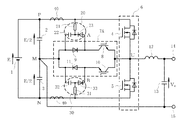
図5は、従来の3レベル電力変換回路の構成図であり、特許文献1に記載されているものである。
図5において、1は直流電源(電圧をEとする),2,3はコンデンサ(各電圧をE/2とする)、4,5は半導体スイッチング素子、6は上下アーム部、7は、コンデンサ2,3同士の接続点(中点)Mとスイッチング素子4,5同士の接続点(交流出力端子)Uとの間に接続された双方向スイッチとしての中間アーム部、8,10は半導体スイッチング素子、9,11はダイオード、12はリアクトル、13はコンデンサ、14,15は出力端子、P,Nはそれぞれ直流電源1(コンデンサ2,3の直列回路)の正極,負極である。
上記構成において、コンデンサ2,3の直列回路、上下アーム部6及び中間アーム部7からなる回路16は、一般にT型3レベルインバータと呼ばれている。
FIG. 5 is a configuration diagram of a conventional three-level power conversion circuit, which is described in
In FIG. 5, 1 is a DC power source (voltage is assumed to be E), 2 and 3 are capacitors (each voltage is assumed to be E / 2), 4 and 5 are semiconductor switching elements, 6 is an upper and lower arm portion, and 7 is a capacitor. An intermediate arm portion as a bidirectional switch connected between a connection point (middle point) M between two and three and a connection point (AC output terminal) U between
In the above configuration, the
ここで、直流電源1の電圧Eが例えば1000[V]である場合、出力電圧Voは200〜480[V]に設定される。また、中間アーム部7のスイッチング素子8,10には、耐圧が600[V]程度のSi(ケイ素)からなるIGBTが使用され、ダイオード9,11には、耐圧が600[V]程度のSiC(炭化ケイ素)からなるSBD(ショットキーバリアダイオード)、または、これと同等に逆回復損失が少なく高速動作可能なダイオードが使用される。更に、上下アーム部6のスイッチング素子4,5には、直流電源1から印加される電圧Eの大きさを考慮して、耐圧が1200[V]程度のSiC−MOSFETやSiC−IGBTが使用されている。
Here, when the voltage E of the
この従来技術において、交流出力端子Uは、スイッチング素子4のオンにより正極Pと、スイッチング素子5のオンにより負極Nと、スイッチング素子8,10のオンにより中点Mと、それぞれ同電位になる。すなわち、この回路によれば、スイッチング素子4,5,8,10のオン状態に応じて3つの電圧レベルを出力することが可能である。
なお、上下アーム部6のスイッチング素子4,5には、直流電源1の電圧Eが印加されるモードがそれぞれ存在するが、中間アーム部7のスイッチング素子8,10にはそのようなモードが存在せず、印加電圧の最大値はE/2であるため、スイッチング素子4,5よりも低耐圧の素子を使用することができる。
In this prior art, the AC output terminal U has the same potential as the positive electrode P when the
The
次に、図6は、特許文献2に記載された3レベル電力変換回路の構成図であり、図5と同様にT型3レベルインバータによって構成されている。
図6において、61,62は直流電源、63,64はコンデンサ、65〜68はIGBT等の半導体スイッチング素子、70はスイッチング素子68の両端と正極Pとの間に接続された電圧クランプ型のスナバ回路、71は抵抗、72はコンデンサ、73はダイオード、80は配線インダクタンスである。ここで、スナバ回路70はRCDスナバ回路と呼ばれている。
Next, FIG. 6 is a configuration diagram of the three-level power conversion circuit described in
In FIG. 6, 61 and 62 are DC power sources, 63 and 64 are capacitors, 65 to 68 are semiconductor switching elements such as IGBTs, and 70 is a voltage clamp type snubber connected between both ends of the
この従来技術において、スイッチング素子65,68が交互にオンする場合、スイッチング素子68のオフによって遮断された中間アーム部の電流はスナバ回路70のダイオード73、コンデンサ72、スイッチング素子67の還流ダイオードを介して中点Mに流れ続ける。これにより、配線インダクタンス80の電流変化率(いわゆるdi/dt)はスナバ回路70がない場合に比べて小さくなるため、過電圧によるスイッチング素子67の破壊を防止することができる。
In this prior art, when the
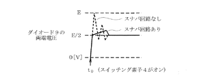
図5に示した従来技術において、上下アーム部6のスイッチング素子4,5は高速でスイッチングするので、例えばスイッチング素子4をオフした際の電流変化率と回路の配線インダクタンスとによって発生するサージ電圧は、図7(a)に示すように大きい値となる。しかし、スイッチング素子4の耐圧を、前述したごとく電源電圧Eより大きめの値に選定しておけば、スイッチング素子4の破壊等の問題を生じることはない。
また、中間アーム部7のスイッチング素子8については、スイッチング速度が比較的遅いため、図7(b)に示すようにサージ電圧が耐圧を超える恐れは少ない。
In the prior art shown in FIG. 5, since the
Further, since the switching speed of the
一方、中間アーム部7のダイオード9には、スイッチング素子4のオンによって電圧(E/2)が逆方向に印加され、回路の配線インダクタンスとダイオード9の寄生キャパシタンスとの共振作用により、図7(c)に示すように耐圧の2倍近いサージ電圧が印加される。
従って、ダイオード9が過電圧破壊される恐れがあり、この現象はスイッチング素子5のオン時におけるダイオード11でも同様に起こり得る。
On the other hand, a voltage (E / 2) is applied to the diode 9 of the
Therefore, the diode 9 may be destroyed by overvoltage, and this phenomenon can occur in the
これらのダイオード9,11の過電圧破壊を防ぐには、通常、高耐圧の素子を使用することが考えられる。しかしながら、ダイオード9,11の本来の印加電圧が600[V]程度であるにも関わらず、例えば耐圧が1200[V]の素子を使用することはコストの増加を招くと共に、高耐圧のダイオードは順電圧降下が大きいため、損失も増加するという問題がある。
In order to prevent the overvoltage breakdown of these
また、図6に示した従来技術では、上下アーム部のスイッチング素子66がオンする場合に、スイッチング素子67,68同士の接続点Sの電位が負極Nの電位となるので、スナバ回路70のコンデンサ72が抵抗71を介して充電され、その両端電圧は直流電源61,62の電圧の和であるEとなる。その後、スイッチング素子66がオフすると、接続点Sの電位は中点Mの電位に戻り、コンデンサ72が抵抗71を介して放電し、コンデンサ72の両端電圧は直流電源61の電圧(E/2)まで低下する。
Further, in the prior art shown in FIG. 6, when the
このように、図6の従来技術では、スイッチング素子66の動作に伴ってスナバ回路70のコンデンサ72が充放電動作を繰り返し、コンデンサ72の電圧は(E/2)の範囲で変化するため、大きな損失が発生する。
図6における接続点Sのように大きな電位変動を起こす部分には、抵抗及びコンデンサからなるスナバ回路(RCスナバ回路)を用いることが有効であるが、一般に、RCスナバ回路のサージ電圧抑制機能は図6のRCDスナバ回路70より劣るものである。また、RCスナバ回路は充放電損失が大きく、このRCスナバ回路を使用する場合には中間アーム部のスイッチング素子68等に高耐圧のものが必要になり、低耐圧のスイッチング素子を使用可能であるという前述した特徴が損なわれてしまう。また、RCスナバ回路は充放電損失が大きく、損失や発熱が増大するという欠点もある。
Thus, in the prior art of FIG. 6, the
Although it is effective to use a snubber circuit (RC snubber circuit) composed of a resistor and a capacitor at a portion where a large potential fluctuation occurs as in the connection point S in FIG. 6, in general, the surge voltage suppression function of the RC snubber circuit is It is inferior to the
そこで、本発明の解決課題は、中間アーム部のダイオードの過電圧破壊を防止すると共に、RCDスナバ回路における損失を低減させた3レベル電力変換回路を提供することにある。 SUMMARY OF THE INVENTION An object of the present invention is to provide a three-level power conversion circuit that prevents overvoltage breakdown of a diode in an intermediate arm portion and reduces loss in an RCD snubber circuit.
上記課題を解決するため、請求項1に係る発明は、直流電圧が印加され、かつ、互いに直列に接続された第1,第2のコンデンサと、前記第1,第2のコンデンサの直列回路に並列に接続された第1,第2のスイッチング素子の直列回路と、前記第1,第2のコンデンサ同士の接続点である中点と前記第1,第2のスイッチング素子同士の接続点である交流出力端子との間に接続された双方向スイッチとしての中間アーム部と、を有し、
前記中間アーム部が、前記中点と前記交流出力端子との間に接続された第1のダイオードと第3のスイッチング素子との直列回路と、前記中点と前記交流出力端子との間に接続された第2のダイオードと第4のスイッチング素子との直列回路と、を備え、
前記第1のダイオードの両端と前記第1,第2のコンデンサ同士の直列回路の正極との間に第1のスナバ回路が接続されると共に、前記第2のダイオードの両端と前記第1,第2のコンデンサ同士の直列回路の負極との間に第2のスナバ回路が接続され、
前記第1〜第4のスイッチング素子の動作により、前記交流出力端子から3つのレベルの電圧を出力させる3レベル電力変換回路において、
互いに順方向に直列接続された前記第1のダイオードと前記第2のダイオードとの接続点を、前記中点に接続したものである。
In order to solve the above-mentioned problem, the invention according to
The intermediate arm portion is connected between a series circuit of a first diode and a third switching element connected between the midpoint and the AC output terminal, and between the midpoint and the AC output terminal. A series circuit of the second diode and the fourth switching element,
A first snubber circuit is connected between both ends of the first diode and a positive electrode of a series circuit of the first and second capacitors, and both ends of the second diode and the first and first A second snubber circuit is connected between the negative electrode of the series circuit of the two capacitors,
In the three-level power conversion circuit that outputs three levels of voltage from the AC output terminal by the operation of the first to fourth switching elements,
A connection point between the first diode and the second diode connected in series in the forward direction is connected to the midpoint.
請求項2に係る発明は、請求項1に記載した3レベル電力変換回路において、
前記第1のスナバ回路が、
前記第1のダイオードに並列に接続され、かつ、前記第1のダイオードに対して順方向に接続された第3のダイオードと第3のコンデンサとの直列回路と、前記第3のダイオードと前記第3のコンデンサとの直列接続点と前記正極との間に接続された第1の抵抗と、によって構成され、
前記第2のスナバ回路が、
前記第2のダイオードに並列に接続され、かつ、前記第2のダイオードに対して順方向に接続された第4のダイオードと第4のコンデンサとの直列回路と、前記第4のダイオードと前記第4のコンデンサとの直列接続点と前記負極との間に接続された第2の抵抗と、によって構成されているものである。
The invention according to
The first snubber circuit comprises:
A series circuit of a third diode and a third capacitor connected in parallel to the first diode and connected in a forward direction with respect to the first diode; the third diode; A first resistor connected between a series connection point of the
The second snubber circuit comprises:
A series circuit of a fourth diode and a fourth capacitor connected in parallel to the second diode and connected in a forward direction with respect to the second diode; the fourth diode; 4 and a second resistor connected between the series connection point with the
請求項3に係る発明は、請求項2に記載した3レベル電力変換回路において、
前記中間アーム部を内蔵したモジュールが、前記第1のダイオードと前記第3のスイッチング素子との接続点に接続された第1の補助端子と、前記第2のダイオードと前記第4のスイッチング素子との接続点に接続された第2の補助端子と、を有し、
前記第1の補助端子が前記第3のダイオードに接続され、前記第2の補助端子が前記第4のダイオードに接続されるものである。
The invention according to
A module incorporating the intermediate arm portion includes a first auxiliary terminal connected to a connection point between the first diode and the third switching element, the second diode, and the fourth switching element. A second auxiliary terminal connected to the connection point of
The first auxiliary terminal is connected to the third diode, and the second auxiliary terminal is connected to the fourth diode.
請求項4に係る発明は、請求項2に記載した3レベル電力変換回路において、
前記中間アーム部を内蔵したモジュールが、前記第1のダイオードと前記第3のスイッチング素子との接続点に前記第3のダイオードを介して接続された第1の補助端子と、前記第2のダイオードと前記第4のスイッチング素子との接続点に前記第4のダイオードを介して接続された第2の補助端子と、を有し、
前記第1の補助端子が前記第3のコンデンサと前記第1の抵抗との接続点に接続され、前記第2の補助端子が前記第4のコンデンサと前記第2の抵抗との接続点に接続されるものである。
The invention according to
A module including the intermediate arm portion; a first auxiliary terminal connected to a connection point between the first diode and the third switching element via the third diode; and the second diode. And a second auxiliary terminal connected to a connection point between the first switching element and the fourth switching element via the fourth diode,
The first auxiliary terminal is connected to a connection point between the third capacitor and the first resistor, and the second auxiliary terminal is connected to a connection point between the fourth capacitor and the second resistor. It is what is done.
本発明によれば、上下アーム部を構成するスイッチング素子のオン時に、中間アーム部のダイオードの寄生キャパシタンスと配線インダクタンとの共振現象によって発生するサージ電圧の放電先を直流回路の正極または負極にすることで、中間アーム部のダイオードの両端電圧を、固定電位点である中点と正極または負極との間の電圧によってクランプする。これにより、中間アーム部のダイオードの過電圧破壊を防止することができると共に、スナバ回路における損失を低減させることが可能である。 According to the present invention, when the switching elements constituting the upper and lower arm portions are turned on, the discharge destination of the surge voltage generated by the resonance phenomenon between the parasitic capacitance of the diode of the intermediate arm portion and the wiring inductance is set to the positive or negative electrode of the DC circuit. Thus, the both-ends voltage of the diode of the intermediate arm portion is clamped by the voltage between the middle point which is the fixed potential point and the positive electrode or the negative electrode. As a result, it is possible to prevent overvoltage breakdown of the diode of the intermediate arm portion and to reduce loss in the snubber circuit.
以下、図に沿って本発明の実施形態を説明する。
図1は、本発明の実施形態を示す構成図であり、図5と同一の機能を有する部分については同一の参照符号を付してある。
Hereinafter, embodiments of the present invention will be described with reference to the drawings.
FIG. 1 is a block diagram showing an embodiment of the present invention, and parts having the same functions as those in FIG. 5 are given the same reference numerals.
図1において、中間アーム部7Aは、前記同様にスイッチング素子8とダイオード9との直列回路、及び、スイッチング素子10とダイオード11との直列回路を並列に接続して構成されており、双方向スイッチとして機能する。ただし、この実施形態では、ダイオード9のアノードとダイオード11のカソードとが安定電位点である中点Mに接続され、スイッチング素子8のエミッタとスイッチング素子10のコレクタとが交流出力端子Uに接続されている。
In FIG. 1, the
直流電源1の電圧Eが、例えば1000[V]である場合、スイッチング素子8,10には、耐圧が600[V]程度のSi−IGBTを使用することができ、ダイオード9,11には、耐圧が600[V]程度のSiC−SBD、または、これと同等に逆回復損失が少なく高速動作可能なダイオードを使用することができる。これに対し、上下アーム部6のスイッチング素子4,5には、耐圧が1200[V]程度のSiC−MOSFETやSiC−IGBTが用いられる。
When the voltage E of the
ダイオード9の両端と直流電源1の正極(コンデンサ2,3の直列回路の正極)Pとの間には、抵抗21、コンデンサ22及びダイオード23からなる電圧クランプ型のRCDスナバ回路20が接続され、ダイオード11の両端と直流電源1の負極(コンデンサ2,3の直列回路の負極)Nとの間にも、抵抗31、コンデンサ32及びダイオード33からなる電圧クランプ型のRCDスナバ回路30が接続されている。
A voltage clamp type
図1に示した構成において、コンデンサ2,3は請求項における第1,第2のコンデンサにそれぞれ相当し、スイッチング素子4,5,8,10は同じく第1,第2,第3,第4のスイッチング素子にそれぞれ相当し、ダイオード9,11は同じく第1,第2のダイオードにそれぞれ相当する。
また、RCDスナバ回路20,30は請求項における第1,第2のスナバ回路にそれぞれ相当する。更に、コンデンサ22,32は第3,第4のコンデンサにそれぞれ相当し、ダイオード23,33は第3,第4のダイオードにそれぞれ相当し、抵抗21,31は第1,第2の抵抗にそれぞれ相当する。
In the configuration shown in FIG. 1, the
The
次に、この実施形態の動作を、図2,図3を参照しつつ説明する。
まず、図2は、上アームのスイッチング素子4がオンした時の動作説明図であり、51は中間アーム部6のスイッチング素子8,10の寄生キャパシタンス、52はダイオード9,11の寄生キャパシタンス、40は回路の配線インダクタンスである。
Next, the operation of this embodiment will be described with reference to FIGS.
First, FIG. 2 is an operation explanatory diagram when the switching
いま、スイッチング素子4がオンするとダイオード9に逆電圧が印加され、ダイオード9の寄生キャパシタンス52に経路aの電流が流れて寄生キャパシタンス52が充電される。
この時、スイッチング素子8の寄生キャパシタンス51はダイオード9の寄生キャパシタンス52に比べて大きいため、スイッチング素子8とダイオード9との直列回路に印加された電圧(E/2)の大部分はダイオード9に加わり、その寄生キャパシタンス52と配線インダクタンス40とによって共振現象が発生する。これにより、仮にスナバ回路20がない場合、図3に破線で示すように、ダイオード9の両端電圧は印加電圧(E/2)の2倍、つまりE近くまで上昇しようとする。
Now, when the switching
At this time, since the
一方、スナバ回路20のコンデンサ22は、平常時に(E/2)まで充電されている。このため、ダイオード9の両端電圧が(E/2)を超えると、電流は経路bによってダイオード9側からコンデンサ22側に転流する。これにより、図3に実線で示すごとく、ダイオード9の両端電圧は(E/2)を僅かに超えた値に抑制され、その後に経路cによる放電によって電圧(E/2)に戻る。
なお、下アームのスイッチング素子5がオンした場合には、ダイオード11側のスナバ回路30の作用により、ダイオード11の電圧は図3と同様に変化することとなる。
On the other hand, the
When the switching
上記のように、本実施形態では、上下アーム部6のスイッチング素子4,5のオン時に寄生キャパシタンス52と配線インダクタンス40との共振現象によって発生するサージ電圧の放電先を正極Pまたは負極Nにすることで、ダイオード9,11の両端電圧を、正極Pまたは負極Nと中点Mとの間の電圧(E/2)によってクランプすることができる。
このため、ダイオード9,11が過電圧破壊される恐れがない。
また、スナバ回路20,30のコンデンサ22,32の電圧変化幅は小さいため、コンデンサ22,32の充放電に伴う損失も低減される。
As described above, in the present embodiment, the discharge destination of the surge voltage generated by the resonance phenomenon between the
For this reason, there is no possibility that the
Moreover, since the voltage change width of the
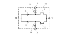
次に、図4は、図1における中間アーム部の変形例を示している。
この変形例は、中間アーム部7Bを一体型のモジュールとして構成したものであり、中間アーム部7Bは、図1のスナバ回路20のダイオード23のアノードに接続される第1の補助端子Aと、スナバ回路30のダイオード33のカソードに接続される第2の補助端子Bとを備えている。なお、図1におけるコンデンサ22,32の各一端(非ダイオード23,33側)は、中点Mに予め接続しておけば良い。
この場合、ダイオード23,33を流れる電流の実効値は小さいため、補助端子A,Bを小型にして抵抗値が比較的大きくても補助端子A,Bの温度上昇が大きくなる恐れはない。
Next, FIG. 4 shows a modification of the intermediate arm portion in FIG.
In this modification, the
In this case, since the effective value of the current flowing through the
また、図4に破線で示すように、図1におけるダイオード23,33を中間アーム部7B側に移しても良い。この場合、第1の補助端子Aはスナバ回路20の抵抗21とコンデンサ22との接続点に接続され、第2の補助端子Bはスナバ回路30の抵抗31とコンデンサ32との接続点に接続されることになる。
上記のように、モジュール化された中間アーム部7Bにダイオード23,33を内蔵することにより、配線の短縮によるスナバ効果の強化が可能である。また、スイッチング素子8,10の冷却手段をダイオード23,33の冷却に兼用することもできる。
Further, as indicated by broken lines in FIG. 4, the
As described above, by incorporating the
本発明は、直流入力電圧が高いパワーコンディショナーシステム等、各種の電力変換システムに利用することができる。 The present invention can be used for various power conversion systems such as a power conditioner system having a high DC input voltage.
1:直流電源
2,3:コンデンサ
4,5,8,10:半導体スイッチング素子
6:上下アーム部
7A,7B:中間アーム部
9,11:ダイオード
12:リアクトル
13:コンデンサ
14,15:出力端子
20,30:RCDスナバ回路
21,31:抵抗
22,32:コンデンサ
23,33:ダイオード
40:配線インダクタンス
51,52:寄生キャパシタンス
P:正極
N:負極
M:中点(接続点)
U:交流出力端子
A,B:補助端子
1:
U: AC output terminal A, B: Auxiliary terminal
Claims (4)
前記中間アーム部が、前記中点と前記交流出力端子との間に接続された第1のダイオードと第3のスイッチング素子との直列回路と、前記中点と前記交流出力端子との間に接続された第2のダイオードと第4のスイッチング素子との直列回路と、を備え、
前記第1のダイオードの両端と前記第1,第2のコンデンサ同士の直列回路の正極との間に第1のスナバ回路が接続されると共に、前記第2のダイオードの両端と前記第1,第2のコンデンサ同士の直列回路の負極との間に第2のスナバ回路が接続され、
前記第1〜第4のスイッチング素子の動作により、前記交流出力端子から3つのレベルの電圧を出力させる3レベル電力変換回路において、
互いに順方向に直列接続された前記第1のダイオードと前記第2のダイオードとの接続点を、前記中点に接続したことを特徴とする3レベル電力変換回路。 A series of first and second switching elements connected in parallel to a series circuit of first and second capacitors to which a DC voltage is applied and connected in series to each other and the first and second capacitors. As a bidirectional switch connected between a circuit and a midpoint that is a connection point between the first and second capacitors and an AC output terminal that is a connection point between the first and second switching elements. An intermediate arm portion,
The intermediate arm portion is connected between a series circuit of a first diode and a third switching element connected between the midpoint and the AC output terminal, and between the midpoint and the AC output terminal. A series circuit of the second diode and the fourth switching element,
A first snubber circuit is connected between both ends of the first diode and a positive electrode of a series circuit of the first and second capacitors, and both ends of the second diode and the first and first A second snubber circuit is connected between the negative electrode of the series circuit of the two capacitors,
In the three-level power conversion circuit that outputs three levels of voltage from the AC output terminal by the operation of the first to fourth switching elements,
A three-level power conversion circuit characterized in that a connection point between the first diode and the second diode connected in series in the forward direction is connected to the midpoint.
前記第1のスナバ回路が、
前記第1のダイオードに並列に接続され、かつ、前記第1のダイオードに対して順方向に接続された第3のダイオードと第3のコンデンサとの直列回路と、前記第3のダイオードと前記第3のコンデンサとの直列接続点と前記正極との間に接続された第1の抵抗と、によって構成され、
前記第2のスナバ回路が、
前記第2のダイオードに並列に接続され、かつ、前記第2のダイオードに対して順方向に接続された第4のダイオードと第4のコンデンサとの直列回路と、前記第4のダイオードと前記第4のコンデンサとの直列接続点と前記負極との間に接続された第2の抵抗と、によって構成されていることを特徴とする3レベル電力変換回路。 The three-level power conversion circuit according to claim 1,
The first snubber circuit comprises:
A series circuit of a third diode and a third capacitor connected in parallel to the first diode and connected in a forward direction with respect to the first diode; the third diode; A first resistor connected between a series connection point of the capacitor 3 and the positive electrode,
The second snubber circuit comprises:
A series circuit of a fourth diode and a fourth capacitor connected in parallel to the second diode and connected in a forward direction with respect to the second diode; the fourth diode; 4. A three-level power conversion circuit comprising: a series connection point with four capacitors; and a second resistor connected between the negative electrode.
前記中間アーム部を内蔵したモジュールが、前記第1のダイオードと前記第3のスイッチング素子との接続点に接続された第1の補助端子と、前記第2のダイオードと前記第4のスイッチング素子との接続点に接続された第2の補助端子と、を有し、
前記第1の補助端子が前記第3のダイオードに接続され、前記第2の補助端子が前記第4のダイオードに接続されることを特徴とする3レベル電力変換回路。 The three-level power conversion circuit according to claim 2,
A module incorporating the intermediate arm portion includes a first auxiliary terminal connected to a connection point between the first diode and the third switching element, the second diode, and the fourth switching element. A second auxiliary terminal connected to the connection point of
The three-level power converter circuit, wherein the first auxiliary terminal is connected to the third diode, and the second auxiliary terminal is connected to the fourth diode.
前記中間アーム部を内蔵したモジュールが、前記第1のダイオードと前記第3のスイッチング素子との接続点に前記第3のダイオードを介して接続された第1の補助端子と、前記第2のダイオードと前記第4のスイッチング素子との接続点に前記第4のダイオードを介して接続された第2の補助端子と、を有し、
前記第1の補助端子が前記第3のコンデンサと前記第1の抵抗との接続点に接続され、前記第2の補助端子が前記第4のコンデンサと前記第2の抵抗との接続点に接続されることを特徴とする3レベル電力変換回路。 The three-level power conversion circuit according to claim 2,
A module including the intermediate arm portion; a first auxiliary terminal connected to a connection point between the first diode and the third switching element via the third diode; and the second diode. And a second auxiliary terminal connected to a connection point between the first switching element and the fourth switching element via the fourth diode,
The first auxiliary terminal is connected to a connection point between the third capacitor and the first resistor, and the second auxiliary terminal is connected to a connection point between the fourth capacitor and the second resistor. A three-level power conversion circuit.
Priority Applications (1)
| Application Number | Priority Date | Filing Date | Title |
|---|---|---|---|
| JP2016076418A JP6714834B2 (en) | 2016-04-06 | 2016-04-06 | 3-level power conversion circuit |
Applications Claiming Priority (1)
| Application Number | Priority Date | Filing Date | Title |
|---|---|---|---|
| JP2016076418A JP6714834B2 (en) | 2016-04-06 | 2016-04-06 | 3-level power conversion circuit |
Publications (2)
| Publication Number | Publication Date |
|---|---|
| JP2017189026A true JP2017189026A (en) | 2017-10-12 |
| JP6714834B2 JP6714834B2 (en) | 2020-07-01 |
Family
ID=60045070
Family Applications (1)
| Application Number | Title | Priority Date | Filing Date |
|---|---|---|---|
| JP2016076418A Active JP6714834B2 (en) | 2016-04-06 | 2016-04-06 | 3-level power conversion circuit |
Country Status (1)
| Country | Link |
|---|---|
| JP (1) | JP6714834B2 (en) |
Cited By (4)
| Publication number | Priority date | Publication date | Assignee | Title |
|---|---|---|---|---|
| CN110350812A (en) * | 2018-04-08 | 2019-10-18 | 佛山科学技术学院 | A kind of inverter module for UPS |
| JP2020025378A (en) * | 2018-08-06 | 2020-02-13 | 富士電機株式会社 | Power conversion device |
| WO2020116338A1 (en) * | 2018-12-06 | 2020-06-11 | ローム株式会社 | Electric power conversion device and control device therefor |
| JP7305114B2 (en) | 2018-12-06 | 2023-07-10 | ローム株式会社 | Power conversion device and its control device |
Citations (7)
| Publication number | Priority date | Publication date | Assignee | Title |
|---|---|---|---|---|
| JPH0583947A (en) * | 1991-09-20 | 1993-04-02 | Hitachi Ltd | Inverter apparatus |
| JPH07312872A (en) * | 1994-05-17 | 1995-11-28 | Fuji Electric Co Ltd | Power converting apparatus and control method therefor |
| WO1998043345A1 (en) * | 1997-03-25 | 1998-10-01 | Mitsubishi Denki Kabushiki Kaisha | Power converter |
| US5910892A (en) * | 1997-10-23 | 1999-06-08 | General Electric Company | High power motor drive converter system and modulation control |
| JP2004096833A (en) * | 2002-08-29 | 2004-03-25 | Toshiba Corp | Power convertor |
| JP2013520150A (en) * | 2010-02-18 | 2013-05-30 | ホッホシューレ コンスタンツ | 3-level pulse width modulation inverter with snubber circuit |
| WO2015049743A1 (en) * | 2013-10-02 | 2015-04-09 | 富士電機株式会社 | Three-level inverter |
-
2016
- 2016-04-06 JP JP2016076418A patent/JP6714834B2/en active Active
Patent Citations (7)
| Publication number | Priority date | Publication date | Assignee | Title |
|---|---|---|---|---|
| JPH0583947A (en) * | 1991-09-20 | 1993-04-02 | Hitachi Ltd | Inverter apparatus |
| JPH07312872A (en) * | 1994-05-17 | 1995-11-28 | Fuji Electric Co Ltd | Power converting apparatus and control method therefor |
| WO1998043345A1 (en) * | 1997-03-25 | 1998-10-01 | Mitsubishi Denki Kabushiki Kaisha | Power converter |
| US5910892A (en) * | 1997-10-23 | 1999-06-08 | General Electric Company | High power motor drive converter system and modulation control |
| JP2004096833A (en) * | 2002-08-29 | 2004-03-25 | Toshiba Corp | Power convertor |
| JP2013520150A (en) * | 2010-02-18 | 2013-05-30 | ホッホシューレ コンスタンツ | 3-level pulse width modulation inverter with snubber circuit |
| WO2015049743A1 (en) * | 2013-10-02 | 2015-04-09 | 富士電機株式会社 | Three-level inverter |
Cited By (6)
| Publication number | Priority date | Publication date | Assignee | Title |
|---|---|---|---|---|
| CN110350812A (en) * | 2018-04-08 | 2019-10-18 | 佛山科学技术学院 | A kind of inverter module for UPS |
| JP2020025378A (en) * | 2018-08-06 | 2020-02-13 | 富士電機株式会社 | Power conversion device |
| JP7099153B2 (en) | 2018-08-06 | 2022-07-12 | 富士電機株式会社 | Power converter |
| WO2020116338A1 (en) * | 2018-12-06 | 2020-06-11 | ローム株式会社 | Electric power conversion device and control device therefor |
| JP7305114B2 (en) | 2018-12-06 | 2023-07-10 | ローム株式会社 | Power conversion device and its control device |
| US11764668B2 (en) | 2018-12-06 | 2023-09-19 | Rohm Co., Ltd. | Control device for controlling an electric power conversion device incorporating a bidirectional inverter |
Also Published As
| Publication number | Publication date |
|---|---|
| JP6714834B2 (en) | 2020-07-01 |
Similar Documents
| Publication | Publication Date | Title |
|---|---|---|
| US11139808B2 (en) | Semiconductor device and power conversion system | |
| US8279639B2 (en) | Direct AC power converting apparatus | |
| US20050041348A1 (en) | Semiconductor switching device | |
| US6169672B1 (en) | Power converter with clamping circuit | |
| JP6714834B2 (en) | 3-level power conversion circuit | |
| JP5228886B2 (en) | Snubber circuit | |
| JP5929277B2 (en) | 3-level power converter | |
| WO2017022693A1 (en) | Three-level chopper device | |
| JP6904091B2 (en) | Gate drive circuit and inverter device | |
| JP2018011467A (en) | Gate drive circuit for semiconductor switching element | |
| JP2957407B2 (en) | Three-level inverter device | |
| JP2020014045A (en) | Bidirectional switch circuit | |
| JPH07312878A (en) | Snubber circuit for three-level inverter | |
| JP5741199B2 (en) | Rectifier snubber circuit | |
| JP5233492B2 (en) | AC / DC converter | |
| WO2017064848A1 (en) | Electric power conversion device and power conditioner using same | |
| JP6028620B2 (en) | 3-level inverter snubber circuit | |
| JP6447944B2 (en) | Power converter and power conditioner using the same | |
| JP4859528B2 (en) | Snubber circuit | |
| JP7147998B2 (en) | Semiconductor vibration suppression circuit | |
| JP2006230042A (en) | Bidirectional switching circuit | |
| JP2001169563A (en) | Three-level inverter | |
| WO1998001940A1 (en) | Power converter | |
| JP4380280B2 (en) | 3-level inverter | |
| JP7384849B2 (en) | power converter |
Legal Events
| Date | Code | Title | Description |
|---|---|---|---|
| A621 | Written request for application examination |
Free format text: JAPANESE INTERMEDIATE CODE: A621 Effective date: 20190314 |
|
| A977 | Report on retrieval |
Free format text: JAPANESE INTERMEDIATE CODE: A971007 Effective date: 20200131 |
|
| A131 | Notification of reasons for refusal |
Free format text: JAPANESE INTERMEDIATE CODE: A131 Effective date: 20200205 |
|
| A521 | Request for written amendment filed |
Free format text: JAPANESE INTERMEDIATE CODE: A523 Effective date: 20200305 |
|
| TRDD | Decision of grant or rejection written | ||
| A01 | Written decision to grant a patent or to grant a registration (utility model) |
Free format text: JAPANESE INTERMEDIATE CODE: A01 Effective date: 20200507 |
|
| A61 | First payment of annual fees (during grant procedure) |
Free format text: JAPANESE INTERMEDIATE CODE: A61 Effective date: 20200520 |
|
| R150 | Certificate of patent or registration of utility model |
Ref document number: 6714834 Country of ref document: JP Free format text: JAPANESE INTERMEDIATE CODE: R150 |
|
| RD02 | Notification of acceptance of power of attorney |
Free format text: JAPANESE INTERMEDIATE CODE: R3D02 |
|
| R250 | Receipt of annual fees |
Free format text: JAPANESE INTERMEDIATE CODE: R250 |