JP2017177696A - Apparatus and method for injection molding - Google Patents
Apparatus and method for injection molding Download PDFInfo
- Publication number
- JP2017177696A JP2017177696A JP2016071640A JP2016071640A JP2017177696A JP 2017177696 A JP2017177696 A JP 2017177696A JP 2016071640 A JP2016071640 A JP 2016071640A JP 2016071640 A JP2016071640 A JP 2016071640A JP 2017177696 A JP2017177696 A JP 2017177696A
- Authority
- JP
- Japan
- Prior art keywords
- mold
- conductive
- injection molding
- cavity
- injection
- Prior art date
- Legal status (The legal status is an assumption and is not a legal conclusion. Google has not performed a legal analysis and makes no representation as to the accuracy of the status listed.)
- Granted
Links
Images


Abstract
Description
本発明は、射出成形装置および射出成形方法に関し、特に、本発明は、導電性材料を用いて射出成形するための射出成形装置および射出成形方法に関する。 The present invention relates to an injection molding apparatus and an injection molding method, and in particular, the present invention relates to an injection molding apparatus and an injection molding method for injection molding using a conductive material.
従来より、射出成形装置を用いて成形品を射出成形する方法は知られている。具体的には、かかる方法は、射出成形装置を用いて樹脂材料を流動可能温度に加熱溶融させる工程、予め型締めされた金型のキャビティ内に溶融樹脂材料を充填する工程、充填した溶融樹脂材料を保圧・冷却させる工程、金型を開いて成形品を取り出す工程から構成される。 Conventionally, a method for injection molding a molded product using an injection molding apparatus is known. Specifically, such a method includes a step of heating and melting a resin material to a flowable temperature using an injection molding apparatus, a step of filling a molten resin material into a cavity of a mold that has been clamped in advance, and a filled molten resin It consists of a process of holding and cooling the material, and a process of opening the mold and taking out the molded product.
射出成形装置を用いて射出成形される成形品として、例えばバンパー等の自動車部品が挙げられる。近年、当該バンパー等の自動車部品の更なる軽量化等のニーズに応えるため、大型かつ薄肉の成形品を射出成形する技術が求められている。大型かつ薄肉の成形品を射出成形する場合、射出圧力が不足すると、キャビティの末端部まで溶融樹脂材料が充填されないおそれがある。 As a molded product that is injection-molded using an injection molding apparatus, for example, automobile parts such as a bumper can be cited. In recent years, in order to meet the needs for further weight reduction of automobile parts such as the bumper, a technique for injection molding a large and thin molded product is required. When injection molding a large and thin molded product, if the injection pressure is insufficient, the molten resin material may not be filled up to the end of the cavity.
射出圧力不足の解消のため射出圧力を高めることが考えられる。しかしながら、射出圧力の大きさに応じた型締圧力による金型の型締めを要するため、高い型締圧力を有する大型の射出成形装置と、射出圧力と型締圧力に耐えうる大型の金型とが必要となる。また、射出圧力不足の解消のためゲート数を増やす方法や成形品の肉厚を厚くする方法も考えられる。しかしながら、ウェルドマークの発生し得る箇所が増加し、材料コストも増加し得る。 It is conceivable to increase the injection pressure in order to eliminate the shortage of injection pressure. However, since the mold needs to be clamped with a clamping pressure corresponding to the magnitude of the injection pressure, a large injection molding apparatus having a high clamping pressure, a large mold capable of withstanding the injection pressure and the clamping pressure, Is required. In addition, a method of increasing the number of gates and a method of increasing the thickness of the molded product to eliminate the shortage of injection pressure can be considered. However, the number of places where a weld mark can occur increases, and the material cost can also increase.
これにつき、特許文献1には、金型の加熱と冷却を繰り返す、所謂ヒートアンドクール成形について開示されている。これによれば、射出時に金型を加熱することで、キャビティ内に射出された樹脂材料が間接的に加熱され、樹脂材料の温度低下が抑制されるので、射出圧力を高め、かつゲート数や成形品の肉厚を変更することなくその樹脂材料の流動性低下を抑制することができる。 In this regard, Patent Document 1 discloses so-called heat and cool molding in which heating and cooling of a mold are repeated. According to this, by heating the mold at the time of injection, the resin material injected into the cavity is indirectly heated, and the temperature drop of the resin material is suppressed, so that the injection pressure is increased and the number of gates is increased. A decrease in fluidity of the resin material can be suppressed without changing the thickness of the molded product.
また、近年、樹脂成形品に対して静電塗装に必要な導電性を付与するために、絶縁性樹脂材料に導電性フィラを混合させて得られる導電性材料が射出成形にて用いられている。これにつき、特許文献2には、射出成形装置のノズルにて、キャビティへの充填前にノズル流路内の導電性材料を通電加熱させる旨が開示されている。
In recent years, conductive materials obtained by mixing conductive fillers with insulating resin materials have been used in injection molding in order to impart conductivity necessary for electrostatic coating to resin molded products. . In this regard,
しかしながら、特許文献1では、充填される溶融樹脂材料に比べ熱容量が大きな金型が加熱されるため金型温度が高くなる。金型温度が高くなると、それに起因して金型を冷却して成形品を冷却するための時間が長くなってしまう。そのため、射出工程から成形品の取出工程までの射出成形サイクルが長期化するおそれがある。 However, in patent document 1, since the metal mold | die with a large heat capacity is heated compared with the molten resin material with which it fills, metal mold | die temperature becomes high. When the mold temperature becomes high, the time required for cooling the mold and cooling the molded product is increased. Therefore, there is a possibility that the injection molding cycle from the injection process to the removal process of the molded product may be prolonged.
特許文献2では、ノズルからキャビティ内に射出される溶融樹脂材料は、キャビティの形成面に触れる表面側から冷却されていく。かかる冷却により溶融樹脂材料が固化状態へと向かうため溶融樹脂材料の流動性が低下する。かかる流動性低下により、キャビティの末端部まで溶融樹脂材料を充填できないおそれがある。
In
特に、少なくとも2つの異なる厚み寸法を有するキャビティを用いて射出成形する場合、溶融樹脂材料の流動性低下によるキャビティ末端部までの溶融樹脂材料の充填不足は、顕著となるおそれがある。そのため、溶融樹脂材料の充填不足に起因した成形品の外観不具合が目立つおそれがある。 In particular, when injection molding is performed using cavities having at least two different thickness dimensions, insufficient filling of the molten resin material up to the end of the cavity due to a decrease in fluidity of the molten resin material may become significant. Therefore, the appearance defect of the molded product due to insufficient filling of the molten resin material may be conspicuous.
そこで、本発明は、少なくとも2つの異なる厚み寸法を有するキャビティに導電性材料を注入して射出成形する場合に、射出成形サイクルの長期化および成形品の外観不具合の発生の抑制を可能とする射出成形装置および射出成形方法を提供することを目的とする。 Therefore, the present invention provides an injection that can prolong the injection molding cycle and suppress the appearance defect of a molded product when a conductive material is injected into a cavity having at least two different thickness dimensions and injection molding is performed. An object is to provide a molding apparatus and an injection molding method.
上記目的を達成するために、本発明の一実施形態では、
導電性材料を流動可能温度に加熱溶融させ、成形型内に射出する加熱射出手段を備えた射出成形装置であって、
成形型は、キャビティの形成面の少なくとも一部に互いに絶縁された複数の導電部を有して成り、
導電部間に所定の電圧を印加する通電手段を備え、
キャビティが少なくとも2つの異なる厚み寸法を有し、異なる厚み寸法の領域ごとに独立した通電回路がそれぞれ形成されている
ことを特徴とする射出成形装置が提供される。
In order to achieve the above object, in one embodiment of the present invention,
An injection molding apparatus comprising a heating and injection means for heating and melting a conductive material to a flowable temperature and injecting it into a mold,
The mold has a plurality of conductive parts insulated from each other on at least a part of the formation surface of the cavity,
Comprising energization means for applying a predetermined voltage between the conductive parts;
There is provided an injection molding apparatus characterized in that the cavity has at least two different thickness dimensions, and an independent energization circuit is formed for each region of different thickness dimensions.
上記目的を達成するために、本発明の一実施形態では、
導電性材料を成形型内に射出して射出成形品を得るための射出成形方法であって、
加熱射出手段を用いて、導電性材料を流動可能温度に加熱溶融させ、成形型内に射出する加熱射出ステップと、
射出された導電性材料が成形型のキャビティの形成面の少なくとも一部に互いに絶縁して設けられた複数の導電部に接触したときに通電加熱されるように、導電部間に電圧を印加する通電ステップと、を含み、
キャビティが少なくとも2つの異なる厚み寸法を有する際において、異なる厚み寸法の領域ごとに独立した通電回路をそれぞれ形成する
ことを特徴とする射出成形方法が提供される。
In order to achieve the above object, in one embodiment of the present invention,
An injection molding method for obtaining an injection molded product by injecting a conductive material into a mold,
A heating and injection step in which the conductive material is heated and melted to a flowable temperature using a heating and injection means, and injected into a mold;
A voltage is applied between the conductive parts so that the injected conductive material is energized and heated when it comes into contact with a plurality of conductive parts insulated from each other on at least a part of the forming surface of the mold cavity. An energization step,
When the cavity has at least two different thickness dimensions, there is provided an injection molding method characterized in that an independent energization circuit is formed for each region of different thickness dimensions.
本発明に従えば、少なくとも2つの異なる厚み寸法を有するキャビティに導電性材料を注入して射出成形する場合に、射出成形サイクルの長期化および成形品の外観不具合の発生抑制を好適に行うことができる。 According to the present invention, when a conductive material is injected into a cavity having at least two different thickness dimensions and injection molding is performed, it is possible to suitably extend the injection molding cycle and suppress the appearance defect of the molded product. it can.
<射出成形装置の一般的構成>
まず、本実施形態の射出成形装置における特徴的構成について説明する前に、本実施形態の射出成形装置の一般的構成について図面を参照しながら説明する。
<General configuration of injection molding device>
First, before describing the characteristic configuration of the injection molding apparatus of the present embodiment, the general configuration of the injection molding apparatus of the present embodiment will be described with reference to the drawings.
図1に示すように、本実施形態の射出成形装置1は、加熱射出装置2と、加熱射出装置2と対向するように設けられた型締装置3と、を有して成る。加熱射出装置2と型締装置3は基台フレーム(図示せず)上に設けられている。
As shown in FIG. 1, the injection molding apparatus 1 of the present embodiment includes a
(加熱射出装置)
加熱射出装置2は射出シリンダ21を備えている。射出シリンダ21の上部には、成形品の原料となるペレット状の熱可塑性樹脂を射出シリンダ21内に供給するためのホッパ22が取り付けられている。射出シリンダ21の周囲には、熱可塑性樹脂を流動可能温度に加熱溶融するためのバンドヒータ23が巻かれている。射出シリンダ21内には、スクリュ24が回転可能かつ進退可能に設けられている。
(Heating injection device)
The heating and
スクリュ24の後方(図1の左方)には、スクリュ24を前進および後退させるための駆動源として用いられる射出用シリンダ装置25が設けられている。射出用シリンダ装置25では、作動油を用いて射出用シリンダ装置25内に設けられた射出用ピストン25aを前進または後退させる。
An
射出用ピストン25aはスクリュ24の後端と接続されており、射出用ピストン25aを射出用シリンダ装置25内にて前進又は後退させることにより、スクリュ24を射出シリンダ21内にて前進または後退可能としている。なお、射出用ピストン25aには、位置検出器が接続されており、かかる位置検出器によってスクリュ24のスクリュ位置が検出される。
The
射出用シリンダ装置25の後方には、スクリュ24を回転させるための駆動源として用いられる計量モータ26が設けられている。加熱射出装置2の構成要素である射出シリンダ21、スクリュ24、射出用シリンダ装置25および計量モータ26は、同一軸上に設けられている。
A
(型締装置)
型締装置3には、金型装置4が設けられる。かかる金型装置4は、可動金型41と固定金型42とから成り、可動金型41と固定金型42は型締め時に相互に対向する型合わせ面を形成するように構成される。型締め時には可動金型41と固定金型42とにより、加熱射出装置2より射出された溶融樹脂材料を注入するためのキャビティCが形成される。また、可動金型41および固定金型42の内部には、冷却水等の冷却液を流すための流路Fがそれぞれ形成されている。型締装置3は、可動金型41が取り付けられる可動側取付板31と、固定金型42が取り付けられる固定側取付板32と、可動側取付板31を前進、後退させるための駆動源として用いられる型締用シリンダ装置33と、を備えている。
(Clamping device)
The mold clamping device 3 is provided with a mold device 4. The mold apparatus 4 includes a
型締用シリンダ装置33内には、直線的に移動可能な型締用ピストン33aが設けられている。型締用ピストン33aは、型締用シリンダ装置33内に供給される作動油により、型締用シリンダ装置33内を前進または後退する。型締用ピストン33aの前端(図1の左端)には、可動側取付板31が接続されており、型締用ピストン33aが型締用シリンダ装置33内を前進または後退することにより、可動側取付板31に取り付けられた可動金型41が前進または後退する。以上により、型締用ピストン33aを前進(図1の左方)させると、可動側取付板31に取り付けられた可動金型41が前進し、それにより型閉および型締が行われる。また、型締用ピストン33aを後退(図1の右方に移動)させると、可動側取付板31に取り付けられた可動金型41が後退し、それにより型開が行われる。
In the mold
なお、可動側取付板31の背面(図1の右面)には、エジェクタ装置が設けられている。かかるエジェクタ装置は、金型装置4が型開きした際にキャビティ内から成形品を押し出して取り出すことができるように構成されている。また、図1では、直動方式の型締装置3を示しているが、型締用シリンダ装置33と可動側取付板31の間にトグル機構を設けたトグル方式の型締装置が用いられてよい。
An ejector device is provided on the back surface (the right surface in FIG. 1) of the movable
本実施形態の射出成形装置1は、金型装置4を冷却するための冷却装置5を更に有して成る。冷却装置5は冷却ポンプ51を有しており、冷却ポンプ51は冷却液の供給配管52と排出配管53を介して可動金型41および固定金型42にそれぞれ接続されている。供給配管52および排出配管53には、冷却液の流れを遮断するための遮断弁54がそれぞれ設けられている。かかる冷却装置5によれば、全ての遮断弁54を開いた状態で冷却ポンプ51を駆動させて、可動金型41および固定金型42の各流路Fに冷却液を環流させることで、可動金型41および固定金型42を冷却可能とする。なお、可動金型41と固定金型42を別々に冷却するために、可動金型冷却用の冷却ポンプと固定金型冷却用の冷却ポンプとがそれぞれ供されてもよい。
The injection molding apparatus 1 of the present embodiment further includes a
冷却液としては、絶縁性液体が用いられてよい。絶縁性液体は、絶縁性液体の冷却性能、金型装置の使用温度(金型装置の最高温度)、耐圧性能(下述の通電装置による最大印加電圧)等に基づいて選定することができる。絶縁性液体としては、例えば、日本工業規格(JIS C 2320)に規格が示された電気絶縁油、フッ素系不活性液体等を用いることができる。絶縁性液体を用いると、下述の通電加熱時における冷却液を介した冷却ポンプ51への漏電を回避することができる。なお、これに限定されることなく、金型装置4の冷却は、冷却手段を用いることなく自然放熱させて行われてもよい。また、金型装置4の冷却は、例えばペルチェ素子等の冷却手段を用いて行われてもよい。
An insulating liquid may be used as the cooling liquid. The insulating liquid can be selected based on the cooling performance of the insulating liquid, the operating temperature of the mold apparatus (maximum temperature of the mold apparatus), the pressure resistance performance (maximum applied voltage by the energizing apparatus described below), and the like. As the insulating liquid, for example, an electrical insulating oil or a fluorine-based inert liquid whose standard is shown in Japanese Industrial Standard (JIS C 2320) can be used. When the insulating liquid is used, it is possible to avoid leakage of electricity to the
<射出成形装置の特徴的構成>
次に、本実施形態の射出成形装置の特徴的構成について説明する。
<Characteristic configuration of injection molding device>
Next, a characteristic configuration of the injection molding apparatus according to the present embodiment will be described.
まず、射出成形装置1に係る金型装置4は以下の特徴を有する。 First, the mold apparatus 4 according to the injection molding apparatus 1 has the following characteristics.
図1に示すように、かかる金型装置4は可動金型41と固定金型42とから成り、可動金型41と固定金型42とから形成されるキャビティCは、少なくとも2つの異なる厚み寸法を有するように構成されている。また、可動金型41と固定金型42とはそれぞれ入れ子式の構造を有している。具体的には、可動金型41は、型外形部43と、絶縁部材45を介して型外形部43の内部に設けられる導電部47とを有する。また、固定金型42は、型外形部44と、絶縁部材46を介して型外形部44の内部に設けられる導電部48とを有する。導電部47および導電部48は、可動金型41と固定金型42とにより形成されるキャビティCの形成面に設けられている。具体的には、導電部47および導電部48は、可動金型41と固定金型42とにより形成されるキャビティCの形成面の少なくとも一部を形作るように設けられている。また、図1に示すように、導電部47と導電部48とは、キャビティCを挟んで相互に対向するように設けられている。
As shown in FIG. 1, the mold apparatus 4 includes a
絶縁部材45、46は、例えば、アルミナ、ジルコニア、窒化ケイ素、炭化ケイ素、ポリテトラフルオロエチレン(PTFE)、パーフルオロアルコキシアルカン(PFA)、ポリフェニレンサルファイド(PPS)、石英、酸化チタン、ポリエーテルエーテルケトン(PEEK)、ポリイミド、ポリアミドイミド等から成る群から少なくとも1つ選択される。かかる絶縁部材45、46は、所望の耐圧性能(下述の通電装置による最大印加電圧)、金型装置4の使用温度(金型装置4の最高温度)等に基づいて選定することができる。また、絶縁部材45、46は、型外形部42、43と導電部47、48間に、例えば、塗布、溶射、スプレー、転写、嵌め込み、インモールド成形、貼り合せ等の方法によって設けることができる。
The insulating
可動金型41と固定金型42との型合わせ面には、導電部47と導電部48との間を電気的に絶縁する絶縁部材49が設けられている。具体的には、絶縁部材49は、型合わせ面において、可動金型41の導電部47の表面領域を覆うように層状に設けられている。なお、絶縁部材49は、これに限定されることなく、可動金型41の導電部47および固定金型42の導電部48の表面領域の少なくとも一方を覆うように層状に設けられていればよい。
An insulating
本実施形態にて、加熱成形装置から射出される樹脂材料として、導電性材料Pが用いられる。導電性材料Pは、樹脂材料に導電性フィラ等の導電性物質を所望の特性に応じて混合したものである。樹脂材料としては、例えば熱可塑性樹脂材料が挙げられる。熱可塑性樹脂材料は、例えば、ポリプロピレン、ポリアミド、ポリスルフェンサルファイド、ポリイミド、ポリエーテルケトン、ポリエーテルエーテルケトン、ABS、ASAおよびポリカーボネイト等から成る群から少なくとも1つ選択される。導電性物質は、例えば、金属繊維、金属粉末、金属フレーク等の金属系導電性物質、炭素繊維、炭素複合繊維、カーボンブラック、黒鉛等の炭素系導電性物質等から成る群から少なくとも1つ選択される。 In this embodiment, the conductive material P is used as the resin material injected from the thermoforming apparatus. The conductive material P is obtained by mixing a resin material and a conductive substance such as a conductive filler in accordance with desired characteristics. An example of the resin material is a thermoplastic resin material. The thermoplastic resin material is, for example, selected from the group consisting of polypropylene, polyamide, polysulfene sulfide, polyimide, polyetherketone, polyetheretherketone, ABS, ASA, polycarbonate, and the like. The conductive material is at least one selected from the group consisting of metal-based conductive materials such as metal fibers, metal powders, and metal flakes, and carbon-based conductive materials such as carbon fibers, carbon composite fibers, carbon black, and graphite. Is done.
また、射出成形装置1は以下の特徴を有する。 Moreover, the injection molding apparatus 1 has the following characteristics.
(導電性材料の通電加熱)
射出成形装置1は、上述の導電部47と導電部48との間に電圧を印加するための通電装置61を備えている。通電装置61は、定電圧を印加可能な直流電源である。なお、通電装置61は、交流電源であってもよい。射出成形装置1の構成要素である加熱射出装置2には、射出シリンダ21内でバンドヒータ23により溶融された導電性材料Pの電気抵抗値を検知するための抵抗センサ62が設けられている。抵抗センサ62から出力されるセンサ信号は、後述する通電制御部140に入力されるように構成されている。
(Electric heating of conductive materials)
The injection molding apparatus 1 includes an
導電部47および導電部48は、導電部47、48間の電気抵抗値を検知するための型内抵抗値センサ63と接続されている。本実施形態では、型内抵抗値センサ63は、キャビティC内に導電性材料Pが充填される前の状態で、導電部48から導電部47に絶縁部材49を介して流れる漏洩電流を検出するためのセンサとして作用する。
The
また、本実施形態の射出成形装置1は、図1に示すように制御ユニット100により制御されている。制御ユニット100は、加熱射出制御部110と、型締制御部120と、冷却制御部130と、通電制御部140とを備えている。加熱射出制御部110は、加熱射出装置2のバンドヒータ23、射出用シリンダ装置25、および計量モータ26を制御するためのものである。型締制御部120は、型締装置3の型締用シリンダ装置33を制御するためのものである。冷却制御部130は、冷却装置5の冷却ポンプ51および各遮断弁54を制御するためのものである。
Moreover, the injection molding apparatus 1 of this embodiment is controlled by the
電圧制御部140は、通電装置61を制御するためのものであって、通電装置61が出力する所定の電圧をオン/オフ制御し、および、通電装置6が出力する電圧値を制御できるように構成されている。具体的には、本実施形態では、下記の射出成形装置1の制御動作の流れにおいても述べるが、通電制御部140は、加熱射出装置2から射出された導電性材料Pが導電部47、48に接触した際に通電加熱されるように、通電装置61により導電部47、48間に印加される電圧を制御する。つまり、導電性材料Pが導電部47、48に接触した際に通電加熱されるように、通電装置61は、導電性材料Pの射出開始にあわせて通電を開始するように通電制御部140により制御されている。
The
なお、上述の「導電性材料Pの通電加熱」の原理について図2を参照しながら説明する。なお、図2等において、符号PLは、可動金型と固定金型とのパーティングラインを示している。 The principle of the above-mentioned “electric heating of the conductive material P” will be described with reference to FIG. In addition, in FIG. 2 etc., code | symbol PL has shown the parting line of a movable metal mold | die and a fixed metal mold | die.
図2に示すように、加熱射出装置2からスプールSを介してキャビティC内に注入される導電性材料Pは、キャビティCの末端部側(図2のキャビティCの上側に相当)に向かって移動しつつ、キャビティの形成面に触れた表面部分から冷却される。ここで、本実施形態では、上述のように通電制御部140の制御下で、通電装置61によって導電部47、48間に電圧が印加される。具体的には、通電制御部140の制御下で、通電装置61によって導電部48が導電部47よりも高電位となるように導電部47、48間に電圧が印加される。かかる電圧印加により、導電部47、48間に位置するキャビティC内の導電性材料Pが、キャビティCの厚み方向にて導電部48側から導電部47側(図2のキャビティ内の波形矢印を参照)へと向かって通電される。つまり、電流が導電部48側からキャビティC内の導電性材料Pを介して導電部47へと流れる。なお、上述のように、導電部47と導電部48とは型合わせ面にて絶縁部材49により相互に絶縁されているため、導電部48から導電部47への直接の通電が回避されると共に、導電部47と導電部48との間にある導電性材料Pに確実に通電することができる。
As shown in FIG. 2, the conductive material P injected into the cavity C from the heating /
かかる通電により、導電性材料Pに含まれる導電性物質が有する電気抵抗によりジュール熱が発生し、それにより導電性材料Pが通電加熱される。ここで言う「通電加熱」とは、広義には電流を通じさせることで被加熱媒体を加熱させることを指す。ここで言う「通電加熱」とは、狭義には金型装置全体を加熱して間接的に被加熱媒体を加熱させるのではなく、被加熱媒体に電流を通じさせて直接的に加熱させることを指す。かかる通電加熱は、導電性材料PがキャビティC内を移動中に行われることになるため、キャビティCの形成面に触れた導電性材料Pの表面部分からの冷却が抑制される。これにより、キャビティC内を移動する導電性材料Pの温度低下が抑制され、導電性材料Pの流動性低下が抑制される。これにより、溶融した導電性材料PをキャビティCの末端部まで充填することができる。つまり、キャビティC内における導電性材料Pの充填不足を解消することができる。その結果、キャビティC内にて導電性材料Pの充填不足に起因したウェルド等の成形品の外観不具合の発生を回避することができる。 Due to such energization, Joule heat is generated due to the electric resistance of the conductive substance contained in the conductive material P, and thereby the conductive material P is energized and heated. The term “electric heating” as used herein refers to heating the medium to be heated by passing an electric current in a broad sense. The term “electric heating” as used herein refers to directly heating the medium to be heated by passing an electric current, rather than heating the entire mold apparatus indirectly to indirectly heat the medium to be heated. . Since the conductive heating is performed while the conductive material P is moving in the cavity C, cooling from the surface portion of the conductive material P that touches the formation surface of the cavity C is suppressed. Thereby, the temperature fall of the electroconductive material P which moves the inside of the cavity C is suppressed, and the fluid fall of the electroconductive material P is suppressed. Thereby, the molten conductive material P can be filled up to the end of the cavity C. That is, the insufficient filling of the conductive material P in the cavity C can be solved. As a result, it is possible to avoid occurrence of appearance defects of a molded product such as a weld due to insufficient filling of the conductive material P in the cavity C.
本実施形態では、導電性材料Pと比べ熱容量が大きな金型装置全体を加熱して間接的に導電性材料Pを加熱させるのではなく、導電性材料Pその物を通電加熱する。そのため、金型装置の温度が必要以上に高くならず、それにより金型装置を冷却して成形品を冷却するための時間の長期化を回避することができる。つまり、射出工程から成形品の取出工程までの射出成形サイクルの長期化を回避することができる。また、本実施形態では、導電性材料の流動性低下によりキャビティC末端部まで導電性材料を十分に充填することができないという問題回避のために、成形品の肉厚を敢えて厚くする必要もない。それ故、肉厚成形品の形成のために導電性材料を不必要に使用することを要しないため、材料コストの増大を回避することができる。 In the present embodiment, the conductive mold P is not heated indirectly by heating the entire mold apparatus having a larger heat capacity than the conductive material P, but the conductive material P itself is energized and heated. Therefore, the temperature of the mold apparatus does not become higher than necessary, and thereby it is possible to avoid an increase in time for cooling the mold apparatus and cooling the molded product. That is, it is possible to avoid lengthening the injection molding cycle from the injection process to the molded product removal process. Further, in this embodiment, it is not necessary to deliberately increase the thickness of the molded product in order to avoid the problem that the conductive material cannot be sufficiently filled up to the end of the cavity C due to the decrease in fluidity of the conductive material. . Therefore, since it is not necessary to use the conductive material unnecessarily for the formation of the thick molded product, an increase in material cost can be avoided.
また、本実施形態によれば、通電制御部140は、加熱射出制御部110から出力される制御信号が示す導電性材料Pの射出状態に基づき通電装置61を作動制御する。そのため、導電性材料Pが射出されるタイミングに合わせて通電が開始されるので、導電性材料Pを効率的に通電加熱することができる。
Further, according to the present embodiment, the
特に、本実施形態では、少なくとも2つの異なる厚み寸法を有するキャビティC内に注入される導電性材料Pの通電加熱の態様に特徴がある。以下、かかる通電加熱を行うための具体的態様について説明する。 In particular, the present embodiment is characterized in a mode of energization heating of the conductive material P injected into the cavity C having at least two different thickness dimensions. Hereinafter, a specific mode for performing such energization heating will be described.
図3に示すように、少なくとも2つの異なる厚み寸法を有するキャビティCは相対的に小さな厚み寸法を有するキャビティ領域C1と相対的に大きな厚み寸法を有するキャビティ領域C2とを有して成る。キャビティCの形成面に設けられる導電部47は、絶縁層45aを介して隣り合う第1サブ導電部47aと第2サブ導電部47bとを有して成る。キャビティCの形成面に設けられる導電部48は、絶縁層46aを介して相互に隣り合う第1サブ導電部48aと第2サブ導電部48bとを有して成る。なお、絶縁層45aは、隣り合う第1サブ導電部47aと第2サブ導電部47bとの間で電圧印加時に生じ得る漏電を防止するために設けられる。同様に、絶縁層46aは、隣り合う第2サブ導電部48aと第2サブ導電部48bとの間で電圧印加時に生じ得る漏電を防止するために設けられる。絶縁層45a、46aは共に、漏電を防止するためのみに設けられる。一方、パーティングライン面に設けられる導電部47、48間を互いに絶縁する絶縁部材49は、漏電防止に加えて型閉じ・型締めに起因した摩耗等の防止のために設けられる。従って、絶縁層45a、46aは漏電防止のためのみに機能すればよいので、絶縁層45a、46aの厚さは絶縁部材49よりも小さくてよい。
As shown in FIG. 3, the cavity C having at least two different thickness dimensions includes a cavity area C1 having a relatively small thickness dimension and a cavity area C2 having a relatively large thickness dimension. The
ここで、一実施形態では、図3に示すように、通電制御部140の制御下で、2つの通電装置(第1通電装置61a、第2通電装置61b)を用いて、各キャビティ領域(C1、C2)の厚み寸法に応じて、各キャビティ領域を挟むように配置された導電部間に異なる電圧が印加される。なお、これに限定されることなく、通電制御部140の制御下で、1つの通電装置を用いて、各キャビティ領域(C1、C2)の厚み寸法に応じて、各キャビティ領域を挟むように配置された導電部間に異なる電圧が印加されてもよい。
Here, in one embodiment, as shown in FIG. 3, under the control of the
具体的には、通電制御部140により、第1通電装置61aは、キャビティ領域C1の相対的に小さな厚み寸法に対応させて、第1サブ導電部47aと第1サブ導電部48aとの間に相対的に低い電圧を印加するように制御される。かかる相対的に低い電圧印加により、キャビティ領域C1内の導電性材料Pが、キャビティ領域C1の厚み方向にて第1サブ導電部48a側から第1サブ導電部47a側へと向かって通電される。つまり、相対的に低い電流が第1サブ導電部48a側からキャビティ領域C1内の導電性材料Pを介して第1サブ導電部47aへと流れる。
Specifically, the
相対的に低い電流が第1サブ導電部48a側からキャビティ領域C1内の導電性材料Pを介して第1サブ導電部47aへと流れると、キャビティ領域C1内の導電性材料Pに含まれる導電性物質が有する電気抵抗により相対的に小さなジュール熱が発生する。これにより、キャビティ領域C1内では、かかる相対的に小さなジュール熱によって導電性材料Pの通電加熱が行われることになる。当該通電加熱は、導電性材料Pがキャビティ領域C1内を移動中に行われることになるため、キャビティ領域C1の形成面に触れた導電性材料Pの表面部分からの冷却が抑制される。これにより、キャビティ領域C1内を移動する導電性材料Pの温度低下が抑制され、キャビティC1内の導電性材料Pの流動性低下が抑制される。
When a relatively low current flows from the first
一方、通電制御部140により、第2通電装置61bは、キャビティ領域C2の相対的に大きな厚み寸法に対応させて、第2サブ導電部47bと第2サブ導電部48bとの間に相対的に高い電圧を印加するように制御される。かかる相対的に高い電圧印加により、キャビティ領域C2内の導電性材料Pが、キャビティ領域C2の厚み方向にて第2サブ導電部48b側から第2サブ導電部47b側へと向かって通電される。つまり、相対的に高い電流が第2サブ導電部48b側からキャビティ領域C2内の導電性材料Pを介して第2サブ導電部47bへと流れる。
On the other hand, the
相対的に高い電流が第2サブ導電部48b側からキャビティ領域C2内の導電性材料Pを介して第2サブ導電部47bへと流れると、キャビティ領域C2内の導電性材料Pに含まれる導電性物質が有する電気抵抗により相対的に大きなジュール熱が発生する。これにより、キャビティ領域C2内では、かかる相対的に大きなジュール熱によって導電性材料Pの通電加熱が行われることになる。当該通電加熱は、導電性材料Pがキャビティ領域C2内を移動中に行われることになるため、キャビティ領域C2の形成面に触れた導電性材料Pの表面部分からの冷却が抑制される。これにより、キャビティ領域C2内を移動する導電性材料Pの温度低下が抑制され、キャビティC2内の導電性材料Pの流動性低下が抑制される。
When a relatively high current flows from the second
以上のように、本実施形態では、通電装置は、各キャビティ領域の厚み寸法に応じて、各キャビティ領域を挟むように配置された導電部間に異なる電圧を印加するように制御されている。具体的には、通電装置は、各キャビティ領域の厚み寸法に比例した所定電圧を、各キャビティ領域を挟むように配置された導電部間に印加するように制御されている。つまり、本実施形態では、少なくとも2つの異なる厚み寸法のキャビティ領域ごとに独立した通電回路がそれぞれ形成されている。通常、少なくとも2つの異なる厚み寸法を有するキャビティC内の導電性材料に、厚み寸法の違いにかかわらず全体として同じ定電圧を印加すると、相対的に大きな厚み寸法を有するキャビティの所定領域内の導電性材料は、相対的に小さな厚み寸法を有するキャビティの所定領域内の導電性材料よりもその厚み寸法に反比例して通電加熱しにくくなる。つまり、相対的に大きな厚み寸法を有するキャビティの所定領域内の導電性材料の通電加熱量と、相対的に小さな厚み寸法を有するキャビティの所定領域内の導電性材料の通電加熱量との間に違いが生じる。これにつき、本実施形態では、各キャビティ領域の厚み寸法に比例した所定電圧を、各キャビティ領域を挟むように配置された導電部間に印加するので、相対的に大きな厚み寸法を有するキャビティの所定領域内の導電性材料の通電加熱量と、相対的に小さな厚み寸法を有するキャビティの所定領域内の導電性材料の通電加熱量との間の違いを無くすことができる。つまり、少なくとも2つの異なる厚み寸法を有するキャビティC内に注入される導電性材料Pの通電加熱を、厚み寸法の違いにかかわらず均一に行うことができる。 As described above, in the present embodiment, the energization device is controlled so as to apply different voltages between the conductive portions arranged so as to sandwich each cavity region in accordance with the thickness dimension of each cavity region. Specifically, the energization device is controlled so as to apply a predetermined voltage proportional to the thickness dimension of each cavity region between the conductive portions arranged so as to sandwich each cavity region. That is, in the present embodiment, an independent energization circuit is formed for each cavity region having at least two different thickness dimensions. Normally, when the same constant voltage is applied to the conductive material in the cavity C having at least two different thickness dimensions as a whole regardless of the difference in thickness dimensions, the conductivity in a predetermined region of the cavity having a relatively large thickness dimension. The conductive material is less likely to be electrically heated than the conductive material in a predetermined region of the cavity having a relatively small thickness dimension in inverse proportion to the thickness dimension. That is, between the energization heating amount of the conductive material in the predetermined region of the cavity having a relatively large thickness dimension and the energization heating amount of the conductive material in the predetermined region of the cavity having a relatively small thickness dimension. A difference is made. In this regard, in the present embodiment, since a predetermined voltage proportional to the thickness dimension of each cavity region is applied between the conductive parts arranged so as to sandwich each cavity region, the predetermined voltage of the cavity having a relatively large thickness dimension is applied. It is possible to eliminate the difference between the energization heating amount of the conductive material in the region and the energization heating amount of the conductive material in the predetermined region of the cavity having a relatively small thickness dimension. That is, the conductive heating of the conductive material P injected into the cavity C having at least two different thickness dimensions can be performed uniformly regardless of the thickness dimension.
かかる均一な通電加熱により、厚み寸法の違いにかかわらずキャビティC内を移動する導電性材料Pの温度低下をより好適に抑制することができる。これにより、導電性材料Pの流動性低下がより好適に抑制され、溶融した導電性材料PをキャビティCの末端部までより好適に充填することができる。その結果、キャビティC内にて導電性材料Pの充填不足に起因したウェルド等の成形品の外観不具合の発生をより好適に回避することができる。 Such uniform energization heating can more suitably suppress the temperature drop of the conductive material P that moves in the cavity C regardless of the thickness dimension. Thereby, the fluidity | liquidity fall of the electroconductive material P is suppressed more suitably, and the molten electroconductive material P can be more suitably filled to the terminal part of the cavity C. As a result, it is possible to more suitably avoid the appearance defect of the molded product such as a weld due to insufficient filling of the conductive material P in the cavity C.
(導電部間の絶縁部材における漏洩電流)
以下、導電部47、48間の絶縁部材49における漏洩電流について図4を参照しながら説明しておく。
(Leakage current in insulation member between conductive parts)
Hereinafter, the leakage current in the insulating
上述の導電部47、48間を相互に絶縁するための絶縁部材49は、射出成形装置1のショット数の増加に従い劣化が進行する。具体的には、絶縁部材49は、例えば、絶縁部材の摩耗、使用温度および使用圧力、並びに通電電圧等によって劣化が進行する。かかる絶縁部材49の劣化の進行により、絶縁部材の絶縁性能が徐々に低下する。図4に示すように、絶縁性能の低下に伴い、通電加熱時に絶縁部材49を介して導電部47、48間を流れる漏洩電流の電流ピーク値が徐々に大きくなる。
The insulating
絶縁部材49は、例えば、打痕、擦り傷、変形、過熱、過圧力、過電圧等の突発的な事象により絶縁性能が急激に低下する場合がある。しかしながら、かかる事象による絶縁性能の急激な低下を事前予測することは困難である。したがって、絶縁部材49の絶縁性能を監視する観点から、ショット毎に絶縁部材49の漏洩電流の電流ピーク値を測定することが好ましい。
The insulation performance of the insulating
そのため、上述の通電制御部140には、絶縁部材49の絶縁状態を判定するための閾値として予め設定された正常値I1、警告値I2、および危険値I3が、内蔵されたメモリ等に記憶されている。正常値I1としては、使用前の絶縁部材49の漏洩電流の電流ピーク値が設定される。所定のショット数において、測定された漏洩電流の電流ピーク値が正常値I1より大きく、警告値I2以下である場合、射出成形装置1による成形品の生産を続行可能であると判定される。電流ピーク値が警告値I2より大きく、危険値I3以下である場合、射出成形装置1の操作者に対して警告を行う必要があると判定される。電流ピーク値が危険値I3以上である場合、生産を停止すべきと判定される。
Therefore, the
<射出成形装置の制御動作の流れ>
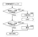
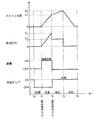
以下、制御ユニット100により制御される射出成形装置1の制御動作の流れについて説明しておく。具体的には、かかる射出成形装置1の制御動作の流れについて、図5〜図7のフローチャートと、スクリュ位置、射出圧力、通電ON/OFF、冷却ポンプのON/OFFの変化を示す図8のタイムチャートと、を参照しながら説明する。なお、以下では、少なくとも2つの異なる厚み寸法を有するキャビティを用いて射出成形する場合を前提とすることを付言しておく。
<Flow of control operation of injection molding device>
Hereinafter, the flow of the control operation of the injection molding apparatus 1 controlled by the
ステップS1
まず、時刻t0において、型締制御部120から出力された型締信号に基づいて型締用シリンダ装置33を駆動させて可動金型41を固定金型42に向かって移動させ、金型装置4を型閉および型締する。この時の型締圧力は、射出時に金型装置4が開かない程度の高い圧力に設定されている。また、型締信号に基づき冷却制御部130は、冷却ポンプ51の駆動を停止する(ONからOFFに切り替える)。
Step S1
First, at
ステップS2
次に、可動金型41と固定金型42の型間絶縁性チェックを実行する。
Step S2
Next, an inter-mold insulation check between the
以下、ステップS2における型間絶縁性チェック工程について、図6を参照しながら具体的に説明する。 Hereinafter, the inter-mold insulation check process in step S2 will be specifically described with reference to FIG.
まず、型内抵抗値センサ63により導電部47、48間を流れる漏洩電流の電流ピーク値を測定する。かかる漏洩電流の電流ピーク値に基づき、電流ピーク値が予め設定された危険値I3より小さいか否かを判定する(ステップS21)。
First, the current peak value of the leakage current flowing between the
ステップS21にて電流ピーク値が危険値I3以上であると判定されると、射出成形装置1による成形品の生産を停止する(ステップS22)。なお、成形品の生産停止後、新たな金型装置4に取り換えて生産を再開してもよい。 If it is determined in step S21 that the current peak value is greater than or equal to the danger value I3, the production of the molded product by the injection molding apparatus 1 is stopped (step S22). Note that after the production of the molded product is stopped, the production may be resumed by replacing with a new mold device 4.
ステップS21で電流ピーク値が危険値I3より小さいと判定されると、電流ピーク値が予め設定された警告値I2より小さいか否かを判定する(ステップS23)。 If it is determined in step S21 that the current peak value is smaller than the dangerous value I3, it is determined whether or not the current peak value is smaller than a preset warning value I2 (step S23).
ステップS23で電流ピーク値が警告値I2以上であると判定されると、例えば、射出成形装置1に設けられたブザー(図示しない)によりアラーム音を発したり、警告灯を点灯、点滅させることで射出成形装置1の操作者に対して警告を行う(ステップS24)。射出成形装置1の操作者に対して警告を行った上で、下記のステップ3に進む。 If it is determined in step S23 that the current peak value is greater than or equal to the warning value I2, for example, an alarm sound is generated by a buzzer (not shown) provided in the injection molding apparatus 1, or a warning light is turned on and blinked. A warning is given to the operator of the injection molding apparatus 1 (step S24). After giving a warning to the operator of the injection molding apparatus 1, the process proceeds to step 3 below.
ステップS23で電流ピーク値が警告値I2より小さいと判定されると、下記のステップ3に進む。 If it is determined in step S23 that the current peak value is smaller than the warning value I2, the process proceeds to step 3 below.
以上により、可動金型41と固定金型42との間の絶縁性をチェックすることができる。
Thus, the insulation between the
ステップS3
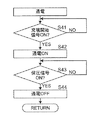
次に、時刻t1において、加熱射出制御部110が射出信号を出力する。かかる射出信号の出力により、加熱射出装置2の射出用シリンダ装置25により予め設定した射出速度でスクリュ24を前進させ、それにより射出シリンダ21から加熱溶融させた導電性材料Pを射出する。次いで、射出した導電性材料PをスプールSを介して少なくとも2つの異なる厚み寸法を有するキャビティC内へと進め、導電性材料Pの充填を開始する。
Step S3
Next, at time t1, the heating and
ステップS4
時刻t1において、通電制御部140は、射出信号に基づき第1通電装置61aおよび第2通電装置61bを制御する(図3参照)。通電制御部140の制御下で、第1通電装置61aにより第1サブ導電部48aと第1サブ導電部47a間にキャビティ領域C1の厚み寸法に比例した所定電圧を印加する。かかる電圧印加により、キャビティ領域C1に位置する導電性材料Pを、第1サブ導電部48a側から第1サブ導電部47a側へと向かって通電させる(図3参照)。つまり、電流が第1サブ導電部48a側からキャビティ領域C1内の導電性材料Pを介して第1サブ導電部47aへと流れる。かかる通電により、キャビティ領域C1内の導電性材料Pに含まれる導電性物質が有する電気抵抗によりジュール熱を発生させ、それにより導電性材料Pを通電加熱する。
Step S4
At time t1, the
また、これと同時に、通電制御部140の制御下で、第2通電装置61bにより第2サブ導電部48bと第2サブ導電部47b間にキャビティ領域C2の厚み寸法(C2の厚み寸法:C1の厚み寸法よりも大)に比例した所定電圧を印加する。かかる電圧印加により、キャビティ領域C2に位置する導電性材料Pを、第2サブ導電部48b側から第2サブ導電部47b側へと向かって通電させる(図3参照)。つまり、電流が第2サブ導電部48b側からキャビティ領域C2内の導電性材料Pを介して第2サブ導電部47bへと流れる。かかる通電により、キャビティ領域C2内の導電性材料Pに含まれる導電性物質が有する電気抵抗によりジュール熱を発生させ、それにより導電性材料Pを通電加熱する。
At the same time, the thickness dimension of the cavity region C2 between the second
以下、ステップS4における通電工程について、図7を参照しながら具体的に説明する。 Hereinafter, the energization process in step S4 will be specifically described with reference to FIG.
まず、加熱射出制御部110から加熱射出装置2に対して出力される射出信号がONか否かを判定する(ステップS41)。
First, it is determined whether or not the injection signal output from the heating /
ステップS41において射出信号がONと判定されると、通電制御部140は、第1通電装置61aと第2通電装置61bに通電をそれぞれ開始させる(ステップS42)。
If it determines with an injection signal being ON in step S41, the electricity
この際、通電制御部140は、加熱射出装置2から射出された導電性材料Pが第1サブ導電部47a、第1サブ導電部48aに接触した際に通電加熱されるように、通電制御部140は、第1通電装置61aにより第1サブ導電部47a、48a間に印加される電圧を制御する。また、かかる制御と同時に、通電制御部140は、加熱射出装置2から射出された導電性材料Pが第2サブ導電部47b、第1サブ導電部48bに接触した際に通電加熱されるように、通電制御部140は、第2通電装置61bにより第2サブ導電部47b、48b間に印加される電圧を制御する。本実施形態では、第1通電装置61aにより第1サブ導電部47a、48a間に予め設定された定電圧が印加される。また、第2通電装置61bにより第2サブ導電部47b、48b間に予め設定された定電圧が印加される。
At this time, the
次に、加熱射出制御部110から加熱射出装置2に対して出力される保圧信号がONか否かを判定する(ステップS43)。
Next, it is determined whether or not the holding pressure signal output from the heating /
ステップS43において保圧信号がONと判定されると、通電装置61(第1通電装置61aおよび第2通電装置61b)の通電を終了し、ステップ5に進む(ステップS44)。
When it is determined in step S43 that the holding pressure signal is ON, the energization of the energization device 61 (the
以上により、加熱射出制御部110から出力される制御信号が示す導電性材料Pの射出状態に基づき通電装置61(第1通電装置61aおよび第2通電装置61b)を制御することができる。
As described above, the energization device 61 (the
ステップS5
次に、スクリュ24がキャビティC内に導電性材料Pが完全充填されるスクリュ位置A1まで前進した時刻t2において、加熱射出制御部110は保圧信号を出力する。かかる保圧信号に基づき加熱射出装置2が制御され、キャビティCに充填した導電性材料Pに対して、予め設定した保圧時間が経過するまで射出充填時の最大圧力よりも低圧である保圧力が付与される。
Step S5
Next, at time t2 when the
ステップS6
次に、保圧時間が経過し、スクリュ24のスクリュ位置がA2まで前進した時刻t3において、予め設定した冷却時間分保圧した導電性材料Pを冷却させる。同時に、加熱射出装置2では、次なるショットのためにバンドヒータ23により導電性材料Pを流動可能温度に加熱溶融すると共に、スクリュ24を回転させ、所定の位置まで後退させる。この際、ホッパ22から供給された導電性材料Pは、射出シリンダ21内において加熱溶融させられ、スクリュ24の後退に伴いスクリュ24の前方に保持される。
Step S6
Next, at time t3 when the pressure holding time has elapsed and the screw position of the
ステップS7
次に、冷却完了の時刻t4において、型締制御部120により型締装置3を制御し、型締用シリンダ装置33の型締用ピストン33aを後退させて金型装置4の型開きを行う。
Step S7
Next, at time t4 when the cooling is completed, the mold
ステップS8
次に、エジェクタ装置によりキャビティC内から成形品を突き出して取り出す。
Step S8
Next, the molded product is ejected from the cavity C by an ejector device.
ステップS9
最後に、成形終了の是非を判定し、成形終了である判定すれば、かかる射出成形サイクルを終了する。
Step S9
Finally, it is determined whether or not the molding is finished. If it is judged that the molding is finished, the injection molding cycle is finished.
上述のように、ステップS4では、各キャビティ領域の厚み寸法に応じて、各キャビティ領域を挟むように配置された導電部間に異なる電圧を印加するように制御されている。具体的には、通電装置は、各キャビティ領域の厚み寸法に比例した所定電圧を、各キャビティ領域を挟むように配置された導電部間に印加するように制御されている。つまり、少なくとも2つの異なる厚み寸法のキャビティ領域ごとに独立した通電回路がそれぞれ形成されている。通常、少なくとも2つの異なる厚み寸法を有するキャビティC内の導電性材料に、厚み寸法の違いにかかわらず全体として同じ定電圧を印加すると、相対的に大きな厚み寸法を有するキャビティの所定領域内の導電性材料は、相対的に小さな厚み寸法を有するキャビティの所定領域内の導電性材料よりもその厚み寸法に反比例して通電加熱しにくくなる。つまり、相対的に大きな厚み寸法を有するキャビティの所定領域内の導電性材料の通電加熱量と、相対的に小さな厚み寸法を有するキャビティの所定領域内の導電性材料の通電加熱量との間に違いが生じる。これにつき、本実施形態では、各キャビティ領域の厚み寸法に比例した所定電圧を、各キャビティ領域を挟むように配置された導電部間に印加するので、相対的に大きな厚み寸法を有するキャビティの所定領域内の導電性材料の通電加熱量と、相対的に小さな厚み寸法を有するキャビティの所定領域内の導電性材料の通電加熱量との間の違いを無くすことができる。つまり、少なくとも2つの異なる厚み寸法を有するキャビティC内に注入される導電性材料Pの通電加熱を、厚み寸法の違いにかかわらず均一に行うことができる。 As described above, in step S4, control is performed so that different voltages are applied between the conductive portions arranged so as to sandwich each cavity region in accordance with the thickness dimension of each cavity region. Specifically, the energization device is controlled so as to apply a predetermined voltage proportional to the thickness dimension of each cavity region between the conductive portions arranged so as to sandwich each cavity region. That is, an independent energization circuit is formed for each cavity region having at least two different thickness dimensions. Normally, when the same constant voltage is applied to the conductive material in the cavity C having at least two different thickness dimensions as a whole regardless of the difference in thickness dimensions, the conductivity in a predetermined region of the cavity having a relatively large thickness dimension. The conductive material is less likely to be electrically heated than the conductive material in a predetermined region of the cavity having a relatively small thickness dimension in inverse proportion to the thickness dimension. That is, between the energization heating amount of the conductive material in the predetermined region of the cavity having a relatively large thickness dimension and the energization heating amount of the conductive material in the predetermined region of the cavity having a relatively small thickness dimension. A difference is made. In this regard, in the present embodiment, since a predetermined voltage proportional to the thickness dimension of each cavity region is applied between the conductive parts arranged so as to sandwich each cavity region, the predetermined voltage of the cavity having a relatively large thickness dimension is applied. It is possible to eliminate the difference between the energization heating amount of the conductive material in the region and the energization heating amount of the conductive material in the predetermined region of the cavity having a relatively small thickness dimension. That is, the conductive heating of the conductive material P injected into the cavity C having at least two different thickness dimensions can be performed uniformly regardless of the thickness dimension.
かかる均一な通電加熱は、導電性材料PがキャビティC内を移動中に行われるため、キャビティC内を移動する導電性材料Pの温度低下を好適に抑制することができる。これにより、導電性材料Pの流動性低下が好適に抑制され、溶融した導電性材料PをキャビティCの末端部まで好適に充填することができる。その結果、キャビティC内にて導電性材料Pの充填不足に起因したウェルド等の成形品の外観不具合の発生を好適に回避することができる。 Such uniform energization heating is performed while the conductive material P is moving in the cavity C, and thus a temperature drop of the conductive material P moving in the cavity C can be suitably suppressed. Thereby, the fluidity | liquidity fall of the electroconductive material P is suppressed suitably, The molten electroconductive material P can be suitably filled to the terminal part of the cavity C. As a result, it is possible to suitably avoid occurrence of appearance defects of a molded product such as a weld due to insufficient filling of the conductive material P in the cavity C.
更に、上述のように、ステップ4では、導電性材料Pそれ自体を通電加熱している。そのため、金型装置の温度が必要以上に高くならず、それにより金型装置を冷却して成形品を冷却するための時間の長期化を回避することができる。つまり、射出工程から成形品の取出工程までの射出成形サイクルの長期化を回避することができる。 Further, as described above, in Step 4, the conductive material P itself is heated by energization. Therefore, the temperature of the mold apparatus does not become higher than necessary, and thereby it is possible to avoid an increase in time for cooling the mold apparatus and cooling the molded product. That is, it is possible to avoid lengthening the injection molding cycle from the injection process to the molded product removal process.
なお、本発明は、例示された実施の形態に限定されるものではなく、本発明の要旨を逸脱しない範囲において、種々の改良および設計上の変更が可能である。 The present invention is not limited to the illustrated embodiments, and various improvements and design changes can be made without departing from the spirit of the present invention.
以上のように、本発明の一実施形態に係る射出成形装置は、バンパー等の自動車部品の製造、液晶ディスプレイ枠等の製造にて好適に利用することができる。 As described above, the injection molding apparatus according to an embodiment of the present invention can be suitably used for manufacturing automobile parts such as bumpers and liquid crystal display frames.
1 射出成形装置
2 加熱射出装置(加熱射出手段)
4 金型装置(成形型)
45a 絶縁層
46a 絶縁層
47、48 導電部
49 絶縁部材(絶縁層)
61 通電装置(通電手段)
C キャビティ
C1 キャビティ領域
C2 キャビティ領域
P 導電性材料
DESCRIPTION OF SYMBOLS 1
4 Mold device (molding tool)
61 Energizing device (energizing means)
C Cavity C1 Cavity region C2 Cavity region P Conductive material
Claims (10)
前記成形型は、キャビティの形成面の少なくとも一部に互いに絶縁された複数の導電部を有して成り、
前記導電部間に所定の電圧を印加する通電手段を備え、
前記キャビティが少なくとも2つの異なる厚み寸法を有し、該異なる厚み寸法の領域ごとに独立した通電回路がそれぞれ形成されている
ことを特徴とする射出成形装置。 An injection molding apparatus comprising a heating and injection means for heating and melting a conductive material to a flowable temperature and injecting it into a mold,
The mold has a plurality of conductive portions insulated from each other on at least a part of a forming surface of the cavity,
Comprising energization means for applying a predetermined voltage between the conductive parts,
The cavity has at least two different thickness dimensions, and an independent energization circuit is formed for each region of the different thickness dimensions.
ことを特徴とする請求項1記載の射出成形装置。 The injection molding apparatus according to claim 1, wherein voltages applied between the conductive portions are controlled in accordance with the thickness dimension.
ことを特徴とする請求項2記載の射出成形装置。 The injection molding apparatus according to claim 2, wherein the voltage proportional to the thickness dimension is applied between the conductive portions.
ことを特徴とする請求項1〜3のいずれかに記載の射出成形装置。 The injection molding apparatus according to any one of claims 1 to 3, wherein an insulating layer for preventing leakage between the energization circuits is provided between the adjacent energization circuits.
ことを特徴とする請求項4記載の射出成形装置。 5. The injection molding apparatus according to claim 4, wherein a thickness of the insulating layer is smaller than a thickness of the insulating layer that insulates the conductive portions provided on the parting line surface of the mold from each other.
加熱射出手段を用いて、前記導電性材料を流動可能温度に加熱溶融させ、前記成形型内に射出する加熱射出ステップと、
射出された前記導電性材料が前記成形型のキャビティの形成面の少なくとも一部に互いに絶縁して設けられた複数の導電部に接触したときに通電加熱されるように、前記導電部間に電圧を印加する通電ステップと、を含み、
前記キャビティが少なくとも2つの異なる厚み寸法を有する際において、該異なる厚み寸法の領域ごとに独立した通電回路をそれぞれ形成する
ことを特徴とする射出成形方法。 An injection molding method for obtaining an injection molded product by injecting a conductive material into a mold,
A heating and injection step in which the conductive material is heated and melted to a flowable temperature using a heating and injection means, and injected into the mold;
A voltage is applied between the conductive parts such that the injected conductive material is energized and heated when it comes into contact with a plurality of conductive parts insulated from each other on at least a part of the forming surface of the mold cavity. Applying an energization step,
An injection molding method, wherein when the cavity has at least two different thickness dimensions, an independent energization circuit is formed for each area of the different thickness dimensions.
ことを特徴とする請求項6記載の射出成形方法。 The injection molding method according to claim 6, wherein a voltage applied between the conductive portions is changed according to the thickness dimension.
ことを特徴とする請求項7記載の射出成形方法。 The injection molding method according to claim 7, wherein the voltage proportional to the thickness dimension is applied between the conductive portions.
ことを特徴とする請求項6〜8のいずれかに記載の射出成形方法。 The injection molding method according to any one of claims 6 to 8, wherein an insulating layer for preventing leakage between the energization circuits is provided between the adjacent energization circuits.
ことを特徴とする請求項9記載の射出成形方法。 10. The injection molding method according to claim 9, wherein the thickness of the insulating layer is made smaller than the thickness of the insulating layer that insulates the conductive parts provided on the parting line surface of the mold from each other.
Priority Applications (1)
| Application Number | Priority Date | Filing Date | Title |
|---|---|---|---|
| JP2016071640A JP6332318B2 (en) | 2016-03-31 | 2016-03-31 | Injection molding apparatus and injection molding method |
Applications Claiming Priority (1)
| Application Number | Priority Date | Filing Date | Title |
|---|---|---|---|
| JP2016071640A JP6332318B2 (en) | 2016-03-31 | 2016-03-31 | Injection molding apparatus and injection molding method |
Publications (2)
| Publication Number | Publication Date |
|---|---|
| JP2017177696A true JP2017177696A (en) | 2017-10-05 |
| JP6332318B2 JP6332318B2 (en) | 2018-05-30 |
Family
ID=60004820
Family Applications (1)
| Application Number | Title | Priority Date | Filing Date |
|---|---|---|---|
| JP2016071640A Expired - Fee Related JP6332318B2 (en) | 2016-03-31 | 2016-03-31 | Injection molding apparatus and injection molding method |
Country Status (1)
| Country | Link |
|---|---|
| JP (1) | JP6332318B2 (en) |
Cited By (2)
| Publication number | Priority date | Publication date | Assignee | Title |
|---|---|---|---|---|
| JP2017177698A (en) * | 2016-03-31 | 2017-10-05 | マツダ株式会社 | Apparatus and method for injection molding |
| JP2017177697A (en) * | 2016-03-31 | 2017-10-05 | マツダ株式会社 | Apparatus and method for injection molding |
Citations (13)
| Publication number | Priority date | Publication date | Assignee | Title |
|---|---|---|---|---|
| JPS4635262Y1 (en) * | 1968-03-29 | 1971-12-04 | ||
| JPS4927566A (en) * | 1972-07-11 | 1974-03-12 | ||
| JPH1058506A (en) * | 1996-08-22 | 1998-03-03 | Meiki Co Ltd | Method for controlling power supply to nozzle heater and power supply controlling apparatus |
| JPH1177780A (en) * | 1997-09-08 | 1999-03-23 | Ricoh Co Ltd | Plastic molding method and apparatus therefor |
| JP2002283392A (en) * | 2001-03-27 | 2002-10-03 | Matsushita Electric Works Ltd | Resin molded product and method for manufacturing the same |
| JP2003311800A (en) * | 2002-04-24 | 2003-11-05 | Ricoh Co Ltd | Method and mold for molding thin plastic molded product |
| JP2003340896A (en) * | 2002-05-30 | 2003-12-02 | Meiki Co Ltd | Method and apparatus for heating molten material in injection molding machine |
| WO2011035376A1 (en) * | 2009-09-24 | 2011-03-31 | Romar Engineering Pty Ltd | A mould or mould core and a method of manufacturing a mould or mould core |
| JP2015199219A (en) * | 2014-04-04 | 2015-11-12 | パナソニックIpマネジメント株式会社 | Method for producing anti-mold resin molded body |
| JP2017177694A (en) * | 2016-03-31 | 2017-10-05 | 宇部興産機械株式会社 | Injection molding device and injection molding method |
| JP2017177697A (en) * | 2016-03-31 | 2017-10-05 | マツダ株式会社 | Apparatus and method for injection molding |
| JP2017177698A (en) * | 2016-03-31 | 2017-10-05 | マツダ株式会社 | Apparatus and method for injection molding |
| JP2017177695A (en) * | 2016-03-31 | 2017-10-05 | マツダ株式会社 | Apparatus and method for injection molding |
-
2016
- 2016-03-31 JP JP2016071640A patent/JP6332318B2/en not_active Expired - Fee Related
Patent Citations (14)
| Publication number | Priority date | Publication date | Assignee | Title |
|---|---|---|---|---|
| JPS4635262Y1 (en) * | 1968-03-29 | 1971-12-04 | ||
| JPS4927566A (en) * | 1972-07-11 | 1974-03-12 | ||
| JPH1058506A (en) * | 1996-08-22 | 1998-03-03 | Meiki Co Ltd | Method for controlling power supply to nozzle heater and power supply controlling apparatus |
| JPH1177780A (en) * | 1997-09-08 | 1999-03-23 | Ricoh Co Ltd | Plastic molding method and apparatus therefor |
| JP2002283392A (en) * | 2001-03-27 | 2002-10-03 | Matsushita Electric Works Ltd | Resin molded product and method for manufacturing the same |
| JP2003311800A (en) * | 2002-04-24 | 2003-11-05 | Ricoh Co Ltd | Method and mold for molding thin plastic molded product |
| JP2003340896A (en) * | 2002-05-30 | 2003-12-02 | Meiki Co Ltd | Method and apparatus for heating molten material in injection molding machine |
| WO2011035376A1 (en) * | 2009-09-24 | 2011-03-31 | Romar Engineering Pty Ltd | A mould or mould core and a method of manufacturing a mould or mould core |
| JP2015199219A (en) * | 2014-04-04 | 2015-11-12 | パナソニックIpマネジメント株式会社 | Method for producing anti-mold resin molded body |
| JP2017177694A (en) * | 2016-03-31 | 2017-10-05 | 宇部興産機械株式会社 | Injection molding device and injection molding method |
| JP2017177697A (en) * | 2016-03-31 | 2017-10-05 | マツダ株式会社 | Apparatus and method for injection molding |
| JP2017177698A (en) * | 2016-03-31 | 2017-10-05 | マツダ株式会社 | Apparatus and method for injection molding |
| WO2017170414A1 (en) * | 2016-03-31 | 2017-10-05 | マツダ株式会社 | Injection molding apparatus and injection molding method |
| JP2017177695A (en) * | 2016-03-31 | 2017-10-05 | マツダ株式会社 | Apparatus and method for injection molding |
Cited By (2)
| Publication number | Priority date | Publication date | Assignee | Title |
|---|---|---|---|---|
| JP2017177698A (en) * | 2016-03-31 | 2017-10-05 | マツダ株式会社 | Apparatus and method for injection molding |
| JP2017177697A (en) * | 2016-03-31 | 2017-10-05 | マツダ株式会社 | Apparatus and method for injection molding |
Also Published As
| Publication number | Publication date |
|---|---|
| JP6332318B2 (en) | 2018-05-30 |
Similar Documents
| Publication | Publication Date | Title |
|---|---|---|
| WO2017170414A1 (en) | Injection molding apparatus and injection molding method | |
| JP6094600B2 (en) | Injection molding apparatus and injection molding method | |
| WO2016111321A1 (en) | Injection molding apparatus and injection molding method | |
| US20070039943A1 (en) | Heatable tool | |
| JP6354780B2 (en) | Injection molding apparatus and injection molding method | |
| JP6332318B2 (en) | Injection molding apparatus and injection molding method | |
| US20180001529A1 (en) | Injection molding with targeted heating of mold cavities in a non-molding position | |
| JP6094601B2 (en) | Injection molding equipment | |
| JP6340631B2 (en) | Injection molding apparatus and injection molding method | |
| JP6323487B2 (en) | Injection molding apparatus and injection molding method | |
| JP2001113580A (en) | Injection molding machine | |
| JP6094603B2 (en) | Injection molding apparatus and injection molding method | |
| JP5928949B2 (en) | Insert molding apparatus and method | |
| KR20160134723A (en) | Injection mold with thermoelectric elements | |
| JP6056879B2 (en) | Injection molding apparatus and injection molding method | |
| JP6056878B2 (en) | Injection molding apparatus and injection molding method | |
| JP6094602B2 (en) | Injection molding apparatus and injection molding method | |
| JP6094607B2 (en) | Injection molding apparatus and injection molding method | |
| JP2004001301A (en) | Die and its manufacturing process | |
| JP6056887B2 (en) | Injection molding apparatus and injection molding method | |
| JP6094608B2 (en) | Injection molding apparatus and injection molding method | |
| JP3813535B2 (en) | Molding method and molding die for plastic thin molded product | |
| US20060051453A1 (en) | Metal mold device method of manufacturing the metal mold device . molding method molded product and molding machine | |
| JP6056886B2 (en) | Injection molding apparatus and injection molding method | |
| JP2004050825A (en) | Die |
Legal Events
| Date | Code | Title | Description |
|---|---|---|---|
| A977 | Report on retrieval |
Free format text: JAPANESE INTERMEDIATE CODE: A971007 Effective date: 20180112 |
|
| A131 | Notification of reasons for refusal |
Free format text: JAPANESE INTERMEDIATE CODE: A131 Effective date: 20180123 |
|
| A521 | Request for written amendment filed |
Free format text: JAPANESE INTERMEDIATE CODE: A523 Effective date: 20180313 |
|
| TRDD | Decision of grant or rejection written | ||
| A01 | Written decision to grant a patent or to grant a registration (utility model) |
Free format text: JAPANESE INTERMEDIATE CODE: A01 Effective date: 20180403 |
|
| A61 | First payment of annual fees (during grant procedure) |
Free format text: JAPANESE INTERMEDIATE CODE: A61 Effective date: 20180416 |
|
| R150 | Certificate of patent or registration of utility model |
Ref document number: 6332318 Country of ref document: JP Free format text: JAPANESE INTERMEDIATE CODE: R150 |
|
| LAPS | Cancellation because of no payment of annual fees |