JP2017163709A - Three-phase inverter and semiconductor module therefor - Google Patents

Three-phase inverter and semiconductor module therefor Download PDF

Info

Publication number
JP2017163709A
JP2017163709A JP2016046175A JP2016046175A JP2017163709A JP 2017163709 A JP2017163709 A JP 2017163709A JP 2016046175 A JP2016046175 A JP 2016046175A JP 2016046175 A JP2016046175 A JP 2016046175A JP 2017163709 A JP2017163709 A JP 2017163709A
Authority
JP
Japan
Prior art keywords
voltage side
cooler
switching element
conductor layer
insulating substrate
Prior art date
Legal status (The legal status is an assumption and is not a legal conclusion. Google has not performed a legal analysis and makes no representation as to the accuracy of the status listed.)
Pending
Application number
JP2016046175A
Other languages
Japanese (ja)
Inventor
勝也 野村
Katsuya Nomura
勝也 野村
小島 崇
Takashi Kojima
崇 小島
佳晋 服部
Yoshikuni Hattori
佳晋 服部
薫 鳥居
Kaoru Torii
薫 鳥居
弘祐 梶
Kosuke Kaji
弘祐 梶
山本 一成
Kazunari Yamamoto
一成 山本
大貴 加藤
Hirotaka Kato
大貴 加藤
Current Assignee (The listed assignees may be inaccurate. Google has not performed a legal analysis and makes no representation or warranty as to the accuracy of the list.)
Toyota Motor Corp
Toyota Central R&D Labs Inc
Original Assignee
Toyota Motor Corp
Toyota Central R&D Labs Inc
Priority date (The priority date is an assumption and is not a legal conclusion. Google has not performed a legal analysis and makes no representation as to the accuracy of the date listed.)
Filing date
Publication date
Application filed by Toyota Motor Corp, Toyota Central R&D Labs Inc filed Critical Toyota Motor Corp
Priority to JP2016046175A priority Critical patent/JP2017163709A/en
Publication of JP2017163709A publication Critical patent/JP2017163709A/en
Pending legal-status Critical Current

Links

Images

Landscapes

  • Inverter Devices (AREA)

Abstract

PROBLEM TO BE SOLVED: To provide a semiconductor module having an easy-to-manufacture structure and capable of satisfying an equilibrium condition of an equivalent bridge circuit of a three-phase inverter.SOLUTION: A semiconductor module 200U includes: high-voltage side insulation substrates 30, 40 and low-voltage side insulation substrates 50, 60. The high-voltage side insulation substrates 30, 40 have high-voltage side intermediate conductor layers 35, 45 provided between first high-voltage side insulator layers 34a, 44a and second high-voltage side insulator layers 34b, 44b. The low-voltage side insulation substrates 50, 60 have low-voltage side intermediate conductor layers 55, 65 provided between first low-voltage side insulator layers 54a, 64a and second low-voltage side insulator layers 54b, 64b. The high-voltage side intermediate conductor layers 35, 45 and the low-voltage side intermediate conductor layers 55, 65 are structured to connect a high-voltage side switching element SW1 with a mid-point MID_U of a low-voltage side switching element SW2.SELECTED DRAWING: Figure 11

Description

本明細書で開示する技術は、三相インバータ及び三相インバータ用の半導体モジュールに関する。   The technology disclosed in this specification relates to a three-phase inverter and a semiconductor module for the three-phase inverter.

例えば電気自動車は、直流電源の直流電力を走行用のモータを駆動するための交流電力に変換する三相インバータを備える。このような三相インバータは、冷却器及び半導体モジュールを備えており、半導体モジュール内のスイッチング素子で発生する熱を冷却器に効率的に伝熱するように構成されている。これにより、三相インバータは、半導体モジュール内のスイッチング素子が高温になることを抑制し、スイッチング素子の安定動作を実現する。   For example, an electric vehicle includes a three-phase inverter that converts DC power of a DC power source into AC power for driving a traveling motor. Such a three-phase inverter includes a cooler and a semiconductor module, and is configured to efficiently transfer heat generated by a switching element in the semiconductor module to the cooler. Thereby, a three-phase inverter suppresses that the switching element in a semiconductor module becomes high temperature, and implement | achieves the stable operation | movement of a switching element.

三相インバータ用の半導体モジュールは、スイッチング素子と冷却器を電気的に絶縁するために、スイッチング素子と冷却器の間に設けられる絶縁基板を有する。絶縁基板は、高周波ノイズに対してコンデンサとして機能する。このため、スイッチング素子と冷却器の間に浮遊容量が形成される。   The semiconductor module for a three-phase inverter has an insulating substrate provided between the switching element and the cooler in order to electrically insulate the switching element and the cooler. The insulating substrate functions as a capacitor against high frequency noise. For this reason, a stray capacitance is formed between the switching element and the cooler.

スイッチング素子は、電力変換するときに高速でスイッチングする。このため、スイッチング素子は、高周波ノイズの発生源となる。これにより、スイッチング素子がスイッチングするときに発生する高周波ノイズは、スイッチング素子から絶縁基板を介して冷却器に流れるコモンモード電流を生成する。   The switching element switches at high speed when power conversion is performed. For this reason, a switching element becomes a generation source of high frequency noise. Thereby, the high frequency noise generated when the switching element switches generates a common mode current flowing from the switching element through the insulating substrate to the cooler.

特許文献1は、三相インバータが動作したときに、三相インバータを構成する回路が等価的にブリッジ回路になることを見出し、その等価ブリッジ回路の平衡条件を満たすようにすることでコモンモード電流を抑える技術を開示する。   Patent Document 1 finds that when a three-phase inverter is operated, a circuit constituting the three-phase inverter becomes an equivalent bridge circuit, and by satisfying the equilibrium condition of the equivalent bridge circuit, the common mode current Disclosure of technology

特開2009−273272号公報JP 2009-273272 A

特許文献1は、等価ブリッジ回路の平衡条件を満たすために、半導体モジュール内において、高電圧側スイッチング素子と冷却器の間の絶縁基板に存在する浮遊容量と低電圧側スイッチング素子と冷却器の間の絶縁基板に存在する浮遊容量の間で容量比を調整する技術を開示する。特許文献1の技術では、そのような容量比を100倍以上にする必要があり、そのためには、絶縁基板間で厚み及び/又は材料を異ならせる必要がある。しかしながら、そのような設計は、以下の理由により容易なことではない。絶縁基板は、高電圧に耐えるための絶縁性能を保つ必要がある。絶縁基板の絶縁性能は厚みに比例するため、絶縁基板の厚みを100分の1に薄くすると、絶縁基板の絶縁性能を保つことが難しい。また、絶縁基板は、冷却器の冷却性能を阻害しないように低い熱抵抗である必要がある。絶縁基板の熱抵抗は厚みに比例するため、絶縁基板の厚みを100倍にすると、冷却器の冷却性能が阻害される。また、絶縁基板の材料は、絶縁性能、低熱抵抗及び機械的強度等を考慮すると、使用できる種類が限定される。このため、絶縁基板間で誘電率が100倍も異なる材料を使用することは、現実的に不可能である。本明細書は、製造が容易な構成の半導体モジュールを有するとともに、等価ブリッジ回路の平衡条件を満たすことができる三相インバータを提供する。また、本明細書は、そのような三相インバータ用の半導体モジュールを提供する。   In Patent Document 1, in order to satisfy the equilibrium condition of the equivalent bridge circuit, the stray capacitance existing on the insulating substrate between the high-voltage side switching element and the cooler and the low-voltage side switching element and the cooler in the semiconductor module. Disclosed is a technique for adjusting a capacitance ratio between stray capacitances existing on an insulating substrate. In the technique of Patent Document 1, it is necessary to increase the capacity ratio to 100 times or more. For this purpose, it is necessary to make the thickness and / or the material different between the insulating substrates. However, such a design is not easy for the following reasons. The insulating substrate needs to maintain an insulating performance for withstanding a high voltage. Since the insulating performance of the insulating substrate is proportional to the thickness, it is difficult to maintain the insulating performance of the insulating substrate when the thickness of the insulating substrate is reduced to 1/100. The insulating substrate needs to have a low thermal resistance so as not to hinder the cooling performance of the cooler. Since the thermal resistance of the insulating substrate is proportional to the thickness, if the thickness of the insulating substrate is increased 100 times, the cooling performance of the cooler is hindered. Moreover, the material which can be used for the insulating substrate is limited in consideration of insulating performance, low thermal resistance, mechanical strength, and the like. For this reason, it is practically impossible to use materials having dielectric constants different by 100 times between insulating substrates. The present specification provides a three-phase inverter that has a semiconductor module that can be easily manufactured and that can satisfy the equilibrium condition of an equivalent bridge circuit. The present specification also provides a semiconductor module for such a three-phase inverter.

本明細書で開示する三相インバータの一実施形態は、冷却器、冷却器で冷却して用いられるとともにU相、V相及びW相を構成する半導体モジュール、高電圧端子及び低電圧端子を備える。半導体モジュールは、各相において、高電圧側スイッチング素子、低電圧側スイッチング素子、高電圧側絶縁基板及び低電圧側絶縁基板を有する。高電圧側絶縁基板と低電圧側絶縁基板は、別体で構成されていてもよく、一体で形成されていてもよい。半導体モジュールは、両面冷却式であってもよく、片面冷却式であってもよい。高電圧側スイッチング素子は、高電圧端子に接続する。低電圧側スイッチング素子は、低電圧端子に接続する。高電圧側スイッチング素子と低電圧側スイッチング素子は、高電圧端子と低電圧端子の間に直列に接続されている。高電圧側絶縁基板は、高電圧側スイッチング素子と冷却器の間に設けられる。低電圧側絶縁基板は、低電圧側スイッチング素子と冷却器の間に設けられる。高電圧側絶縁基板は、高電圧側スイッチング素子側に配置されている第1高電圧側絶縁体層、冷却器側に配置されている第2高電圧側絶縁体層、及び、第1高電圧側絶縁体層と第2高電圧側絶縁体層の間に設けられている高電圧側中間導体層を有する。低電圧側絶縁基板は、低電圧側スイッチング素子側に配置されている第1低電圧側絶縁体層、冷却器側に配置されている第2低電圧側絶縁体層、及び、第1低電圧側絶縁体層と第2低電圧側絶縁体層の間に設けられている低高電圧側中間導体層を有する。高電圧側中間導体層及び低電圧側中間導体層が、高電圧側スイッチング素子と低電圧側スイッチング素子の中点に接続するように構成されている。   One embodiment of the three-phase inverter disclosed in the present specification includes a cooler, a semiconductor module that is used by being cooled by the cooler, and constitutes a U phase, a V phase, and a W phase, a high voltage terminal, and a low voltage terminal. . The semiconductor module includes a high voltage side switching element, a low voltage side switching element, a high voltage side insulating substrate, and a low voltage side insulating substrate in each phase. The high voltage side insulating substrate and the low voltage side insulating substrate may be configured separately or may be integrally formed. The semiconductor module may be a double-sided cooling type or a single-sided cooling type. The high voltage side switching element is connected to the high voltage terminal. The low voltage side switching element is connected to the low voltage terminal. The high voltage side switching element and the low voltage side switching element are connected in series between the high voltage terminal and the low voltage terminal. The high voltage side insulating substrate is provided between the high voltage side switching element and the cooler. The low voltage side insulating substrate is provided between the low voltage side switching element and the cooler. The high voltage side insulating substrate includes a first high voltage side insulator layer disposed on the high voltage side switching element side, a second high voltage side insulator layer disposed on the cooler side, and a first high voltage. A high-voltage-side intermediate conductor layer provided between the side-insulator layer and the second high-voltage-side insulator layer; The low voltage side insulating substrate includes a first low voltage side insulator layer disposed on the low voltage side switching element side, a second low voltage side insulator layer disposed on the cooler side, and a first low voltage. A low high voltage side intermediate conductor layer provided between the side insulator layer and the second low voltage side insulator layer; The high voltage side intermediate conductor layer and the low voltage side intermediate conductor layer are configured to be connected to a midpoint between the high voltage side switching element and the low voltage side switching element.

上記実施形態の三相インバータの等価ブリッジ回路は、それ自体で平衡条件を満たすように構成される。このため、上記実施形態の三相インバータで用いられる半導体モジュールは、その絶縁基板の厚み及び/又は材料に対する設計自由度が高く、製造が簡易な構成を有する。   The equivalent bridge circuit of the three-phase inverter of the above embodiment is configured so as to satisfy the equilibrium condition itself. For this reason, the semiconductor module used in the three-phase inverter of the above-described embodiment has a configuration that has a high degree of design freedom with respect to the thickness and / or material of the insulating substrate and is easy to manufacture.

高電圧側絶縁基板は、各相間において共通形態であるのが望ましい。さらに、低電圧側絶縁基板は、各相間において共通形態であるのが望ましい。この場合、三相インバータの等価ブリッジ回路は、平衡条件が良好に満たされる。   It is desirable that the high voltage side insulating substrate has a common form between the phases. Furthermore, it is desirable that the low-voltage side insulating substrate has a common form between the phases. In this case, the equilibrium condition is satisfactorily satisfied in the equivalent bridge circuit of the three-phase inverter.

インバータの回路構成を示す。The circuit structure of an inverter is shown. 従来技術の両面冷却式の半導体モジュールの要部断面図を模式的に示す。The principal part sectional drawing of the double-sided cooling type semiconductor module of a prior art is typically shown. 従来技術の両面冷却式の半導体モジュールの等価回路を示す。The equivalent circuit of the double-sided cooling type semiconductor module of a prior art is shown. 従来技術の両面冷却式の半導体モジュールの等価回路を示す。The equivalent circuit of the double-sided cooling type semiconductor module of a prior art is shown. 従来技術のインバータの等価回路を示す。The equivalent circuit of the inverter of a prior art is shown. 従来技術のインバータが動作したときの等価回路を示す。An equivalent circuit when a prior art inverter operates is shown. 従来技術のインバータが動作したときの等価回路を示す。An equivalent circuit when a prior art inverter operates is shown. 従来技術のインバータが動作したときの等価回路を示す。An equivalent circuit when a prior art inverter operates is shown. 従来技術のインバータが動作したときの等価回路を示す。An equivalent circuit when a prior art inverter operates is shown. 一般的なブリッジ回路の構成を示す。The structure of a general bridge circuit is shown. 本明細書で開示する両面冷却式の半導体モジュールの要部断面図を模式的に示す。The principal part sectional drawing of the double-sided cooling type semiconductor module disclosed by this specification is typically shown. 本明細書で開示する両面冷却式の半導体モジュールの等価回路を示す。2 shows an equivalent circuit of a double-sided cooling type semiconductor module disclosed in the present specification. 本明細書で開示する両面冷却式の半導体モジュールの等価回路を示す。2 shows an equivalent circuit of a double-sided cooling type semiconductor module disclosed in the present specification. 本明細書で開示するインバータが動作したときの等価回路を示す。6 shows an equivalent circuit when the inverter disclosed in this specification operates. 本明細書で開示するインバータが動作したときの等価回路を示す。6 shows an equivalent circuit when the inverter disclosed in this specification operates. 本明細書で開示するインバータが動作したときの等価回路を示す。6 shows an equivalent circuit when the inverter disclosed in this specification operates. 本明細書で開示するインバータが動作したときの等価回路を示す。6 shows an equivalent circuit when the inverter disclosed in this specification operates. 本明細書で開示する片面冷却式の半導体モジュールの要部断面図を模式的に示す。The principal part sectional drawing of the single-sided cooling-type semiconductor module disclosed by this specification is typically shown.

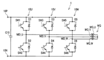
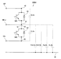
まず、本明細書で開示する技術の理解を助けるために、三相インバータが動作したときに、三相インバータを構成する回路が等価的にブリッジ回路になることを説明する。図1は、例えば電気自動車に搭載して用いられる三相インバータ1の回路構成を例示する。三相インバータ1は、直流電源(図示省略)の直流電力を走行用のモータMGを駆動するための交流電力に変換する。   First, in order to help understanding of the technology disclosed in this specification, it will be described that when a three-phase inverter operates, a circuit constituting the three-phase inverter becomes an equivalent bridge circuit. FIG. 1 exemplifies a circuit configuration of a three-phase inverter 1 used by being mounted on an electric vehicle, for example. The three-phase inverter 1 converts DC power from a DC power supply (not shown) into AC power for driving the traveling motor MG.

三相インバータ1は、高電圧端子10P、低電圧端子10N、平滑コンデンサC10及び3つのレグ10U,10V,10Wを備える。高電圧端子10Pは直流電源(図示省略)の正極に接続され、低電圧端子10Nは直流電源(図示省略)の負極に接続される。三相インバータ1と直流電源(図示省略)の間には、変圧用のコンバータが接続されてもよい。   The three-phase inverter 1 includes a high voltage terminal 10P, a low voltage terminal 10N, a smoothing capacitor C10, and three legs 10U, 10V, and 10W. The high voltage terminal 10P is connected to the positive electrode of a DC power supply (not shown), and the low voltage terminal 10N is connected to the negative electrode of a DC power supply (not shown). A transformer for transformation may be connected between the three-phase inverter 1 and a DC power supply (not shown).

平滑コンデンサC10は、一端が高電圧端子10Pに接続されており、他端が低電圧端子10Nに接続されている。平滑コンデンサC10は、高電圧端子10Pと低電圧端子10Nに入力する交流電力を平滑化する。   The smoothing capacitor C10 has one end connected to the high voltage terminal 10P and the other end connected to the low voltage terminal 10N. The smoothing capacitor C10 smoothes the AC power input to the high voltage terminal 10P and the low voltage terminal 10N.

3つのレグ10U,10V,10Wは、高電圧端子10Pと低電圧端子10Nの間で並列に接続されており、各々が2つのスイッチング素子を有する。後述するように、レグ10U,10V,10Wの各々は、半導体モジュールとして構成されている。   The three legs 10U, 10V, and 10W are connected in parallel between the high voltage terminal 10P and the low voltage terminal 10N, and each has two switching elements. As will be described later, each of the legs 10U, 10V, and 10W is configured as a semiconductor module.

U相レグ10Uは、高電圧端子10Pに接続されている第1スイッチング素子SW1及び低電圧端子10Nに接続されている第2スイッチング素子SW2を有する。第1スイッチング素子SW1と第2スイッチング素子SW2は、高電圧端子10Pと低電圧端子10Nの間で直列に接続されている。第1スイッチング素子SW1と第2スイッチング素子SW2の間のU相中点MID_Uが、モータMGのU相巻線MG_Uの一端に接続されている。第1スイッチング素子SW1に対して逆並列に第1ダイオードD1が接続されており、第2スイッチング素子SW2に対して逆並列に第2ダイオードD2が接続されている。   The U-phase leg 10U includes a first switching element SW1 connected to the high voltage terminal 10P and a second switching element SW2 connected to the low voltage terminal 10N. The first switching element SW1 and the second switching element SW2 are connected in series between the high voltage terminal 10P and the low voltage terminal 10N. U-phase midpoint MID_U between first switching element SW1 and second switching element SW2 is connected to one end of U-phase winding MG_U of motor MG. A first diode D1 is connected in antiparallel to the first switching element SW1, and a second diode D2 is connected in antiparallel to the second switching element SW2.

V相レグ10Vは、高電圧端子10Pに接続されている第3スイッチング素子SW3及び低電圧端子10Nに接続されている第4スイッチング素子SW4を有する。第3スイッチング素子SW3と第4スイッチング素子SW4は、高電圧端子10Pと低電圧端子10Nの間で直列に接続されている。第3スイッチング素子SW3と第4スイッチング素子SW4の間のV相中点MID_Vが、モータMGのV相巻線MG_Vの一端に接続されている。第3スイッチング素子SW3に対して逆並列に第3ダイオードD3が接続されており、第4スイッチング素子SW4に対して逆並列に第4ダイオードD4が接続されている。   The V-phase leg 10V includes a third switching element SW3 connected to the high voltage terminal 10P and a fourth switching element SW4 connected to the low voltage terminal 10N. The third switching element SW3 and the fourth switching element SW4 are connected in series between the high voltage terminal 10P and the low voltage terminal 10N. V-phase midpoint MID_V between third switching element SW3 and fourth switching element SW4 is connected to one end of V-phase winding MG_V of motor MG. A third diode D3 is connected in antiparallel to the third switching element SW3, and a fourth diode D4 is connected in antiparallel to the fourth switching element SW4.

W相レグ10Wは、高電圧端子10Pに接続されている第5スイッチング素子SW5及び低電圧端子10Nに接続されている第6スイッチング素子SW6を有する。第5スイッチング素子SW5と第6スイッチング素子SW6は、高電圧端子10Pと低電圧端子10Nの間で直列に接続されている。第5スイッチング素子SW5と第6スイッチング素子SW6の間のW相中点MID_Wが、モータMGのW相巻線MG_Wの一端に接続されている。第5スイッチング素子SW5に対して逆並列に第5ダイオードD5が接続されており、第6スイッチング素子SW6に対して逆並列に第6ダイオードD6が接続されている。   The W-phase leg 10W includes a fifth switching element SW5 connected to the high voltage terminal 10P and a sixth switching element SW6 connected to the low voltage terminal 10N. The fifth switching element SW5 and the sixth switching element SW6 are connected in series between the high voltage terminal 10P and the low voltage terminal 10N. A W-phase midpoint MID_W between the fifth switching element SW5 and the sixth switching element SW6 is connected to one end of the W-phase winding MG_W of the motor MG. A fifth diode D5 is connected in antiparallel to the fifth switching element SW5, and a sixth diode D6 is connected in antiparallel to the sixth switching element SW6.

スイッチング素子とダイオードの組合せのうちの高電圧端子10Pに接続されるスイッチング素子SW1,SW3,SW5とダイオードD1,D3,D5の組合せは、上アームと称される。スイッチング素子とダイオードの組合せのうちの低電圧端子10Nに接続されるスイッチング素子SW2,SW4,SW6とダイオードD2,D4,D6の組合せは、下アームと称される。上アームのスイッチング素子SW1,SW3,SW5が特許請求の範囲に記載の高電圧側スイッチング素子の一例であり、下アームのスイッチング素子SW2,SW4,SW6が特許請求の範囲に記載の低電圧側スイッチング素子の一例である。   Of the combinations of switching elements and diodes, the combination of switching elements SW1, SW3, SW5 and diodes D1, D3, D5 connected to the high voltage terminal 10P is referred to as an upper arm. Of the combinations of switching elements and diodes, the combination of switching elements SW2, SW4, SW6 and diodes D2, D4, D6 connected to the low voltage terminal 10N is referred to as a lower arm. The upper-arm switching elements SW1, SW3, and SW5 are examples of the high-voltage side switching elements described in the claims, and the lower-arm switching elements SW2, SW4, and SW6 are the low-voltage side switching elements described in the claims. It is an example of an element.

三相インバータ1を構成するスイッチング素子SW1−SW6には、MOSFET(Metal Oxide Semiconductor Field Effect Transistor)又はIGBT(Insulated Gate Bipolar Transistor)が用いられる。また、これらスイッチング素子SW1−SW6は、対応するダイオードD1−D6が一体化された逆導通IGBTであってもよい。以下では、スイッチング素子SW1−SW6がIGBTの場合を例示する。   MOSFETs (Metal Oxide Semiconductor Field Effect Transistors) or IGBTs (Insulated Gate Bipolar Transistors) are used for the switching elements SW1 to SW6 constituting the three-phase inverter 1. Further, these switching elements SW1 to SW6 may be reverse conducting IGBTs in which corresponding diodes D1 to D6 are integrated. Below, the case where switching element SW1-SW6 is IGBT is illustrated.

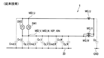
図2に、U相レグ10Uを構成するU相半導体モジュール100Uの要部断面図を模式的に示す。図2に示すU相半導体モジュール100Uは、従来技術の一例である。なお、他のV相レグ10V及びW相レグ10Wも共通形態の半導体モジュールを有する。したがって、以下では、U相半導体モジュール100Uのみを説明し、他のレグ10V,10Wの半導体モジュールの説明を省略する。   FIG. 2 schematically shows a cross-sectional view of the main part of the U-phase semiconductor module 100U constituting the U-phase leg 10U. A U-phase semiconductor module 100U shown in FIG. 2 is an example of a conventional technique. The other V-phase leg 10V and W-phase leg 10W also have a common type semiconductor module. Therefore, hereinafter, only the U-phase semiconductor module 100U will be described, and the description of the other leg 10V, 10W semiconductor modules will be omitted.

U相半導体モジュール100Uは、両面冷却式の半導体モジュールであり、対向する冷却器20の間に介挿される。U相半導体モジュール100Uは、第1スイッチング素子SW1及び第1ダイオードD1を含む半導体チップ2に対応した2つの絶縁基板30,40を有する。U相半導体モジュール100Uはさらに、第2スイッチング素子SW2及び第2ダイオードD2を含む半導体チップ4に対応した2つの絶縁基板50,60を有する。   The U-phase semiconductor module 100U is a double-sided cooling type semiconductor module, and is interposed between the opposing coolers 20. The U-phase semiconductor module 100U includes two insulating substrates 30 and 40 corresponding to the semiconductor chip 2 including the first switching element SW1 and the first diode D1. The U-phase semiconductor module 100U further includes two insulating substrates 50 and 60 corresponding to the semiconductor chip 4 including the second switching element SW2 and the second diode D2.

第1絶縁基板30は、第1スイッチング素子SW1及び第1ダイオードD1を含む半導体チップ2と冷却器20の間に設けられており、チップ側導体層32、絶縁体層34及び冷却器側導体層36を有する。チップ側導体層32、絶縁体層34及び冷却器側導体層36はこの順でチップ2から冷却器20に向けて積層しており、絶縁体層34がチップ側導体層32と冷却器側導体層36を絶縁する。チップ側導体層32が第1スイッチング素子SW1のエミッタ及び第1ダイオードD1のアノードに接続しており、冷却器側導体層36が冷却器20に接続する。   The first insulating substrate 30 is provided between the semiconductor chip 2 including the first switching element SW1 and the first diode D1 and the cooler 20, and includes a chip-side conductor layer 32, an insulator layer 34, and a cooler-side conductor layer. 36. The chip-side conductor layer 32, the insulator layer 34, and the cooler-side conductor layer 36 are laminated in this order from the chip 2 toward the cooler 20, and the insulator layer 34 forms the chip-side conductor layer 32 and the cooler-side conductor. Insulate layer 36. The chip-side conductor layer 32 is connected to the emitter of the first switching element SW1 and the anode of the first diode D1, and the cooler-side conductor layer 36 is connected to the cooler 20.

第2絶縁基板40は、第1スイッチング素子SW1及び第1ダイオードD1を含む半導体チップ2と冷却器20の間に設けられており、チップ側導体層42、絶縁体層44及び冷却器側導体層46を有する。チップ側導体層42、絶縁体層44及び冷却器側導体層46はこの順でチップ2から冷却器20に向けて積層しており、絶縁体層44がチップ側導体層42と冷却器側導体層46を絶縁する。チップ側導体層42が第1スイッチング素子SW1のコレクタ及び第1ダイオードD1のカソードに接続しており、冷却器側導体層46が冷却器20に接続する。   The second insulating substrate 40 is provided between the semiconductor chip 2 including the first switching element SW1 and the first diode D1 and the cooler 20, and includes a chip-side conductor layer 42, an insulator layer 44, and a cooler-side conductor layer. 46. The chip side conductor layer 42, the insulator layer 44, and the cooler side conductor layer 46 are laminated in this order from the chip 2 toward the cooler 20, and the insulator layer 44 includes the chip side conductor layer 42 and the cooler side conductor. Insulate layer 46. The chip-side conductor layer 42 is connected to the collector of the first switching element SW1 and the cathode of the first diode D1, and the cooler-side conductor layer 46 is connected to the cooler 20.

第3絶縁基板50は、第2スイッチング素子SW2及び第2ダイオードD2を含む半導体チップ4と冷却器20の間に設けられており、チップ側導体層52、絶縁体層54及び冷却器側導体層56を有する。チップ側導体層52、絶縁体層54及び冷却器側導体層56はこの順でチップ4から冷却器20に向けて積層しており、絶縁体層54がチップ側導体層52と冷却器側導体層56を絶縁する。チップ側導体層52が第2スイッチング素子SW2のコレクタ及び第2ダイオードD2のカソードに接続しており、冷却器側導体層56が冷却器20に接続する。   The third insulating substrate 50 is provided between the semiconductor chip 4 including the second switching element SW2 and the second diode D2 and the cooler 20, and includes a chip-side conductor layer 52, an insulator layer 54, and a cooler-side conductor layer. 56. The chip-side conductor layer 52, the insulator layer 54, and the cooler-side conductor layer 56 are laminated in this order from the chip 4 toward the cooler 20, and the insulator layer 54 forms the chip-side conductor layer 52 and the cooler-side conductor. Insulate layer 56. The chip-side conductor layer 52 is connected to the collector of the second switching element SW2 and the cathode of the second diode D2, and the cooler-side conductor layer 56 is connected to the cooler 20.

第4絶縁基板60は、第2スイッチング素子SW2及び第2ダイオードD2を含む半導体チップ4と冷却器20の間に設けられており、チップ側導体層62、絶縁体層64及び冷却器側導体層66を有する。チップ側導体層62、絶縁体層64及び冷却器側導体層66はこの順でチップ4から冷却器20に向けて積層しており、絶縁体層64がチップ側導体層62と冷却器側導体層66を絶縁する。チップ側導体層62が第2スイッチング素子SW2のコレクタ及び第2ダイオードD2のカソードに接続しており、冷却器側導体層66が冷却器20に接続する。   The fourth insulating substrate 60 is provided between the semiconductor chip 4 including the second switching element SW2 and the second diode D2 and the cooler 20, and includes a chip-side conductor layer 62, an insulator layer 64, and a cooler-side conductor layer. 66. The chip side conductor layer 62, the insulator layer 64, and the cooler side conductor layer 66 are laminated in this order from the chip 4 toward the cooler 20, and the insulator layer 64 forms the chip side conductor layer 62 and the cooler side conductor. Insulate layer 66. The chip-side conductor layer 62 is connected to the collector of the second switching element SW2 and the cathode of the second diode D2, and the cooler-side conductor layer 66 is connected to the cooler 20.

第2絶縁基板40のチップ側導体層42が高電圧端子10Pに接続されており、第3絶縁基板50のチップ側導体層52が低電圧端子10Nに接続されている。第1絶縁基板30のチップ側導体層32と第4絶縁基板60のチップ側導体層62は、接続配線72を介して接続しており、U相中点MID_Uを構成する。   The chip side conductor layer 42 of the second insulating substrate 40 is connected to the high voltage terminal 10P, and the chip side conductor layer 52 of the third insulating substrate 50 is connected to the low voltage terminal 10N. The chip-side conductor layer 32 of the first insulating substrate 30 and the chip-side conductor layer 62 of the fourth insulating substrate 60 are connected via the connection wiring 72 and constitute the U-phase midpoint MID_U.

このように、絶縁基板30,40,50,60の各々は、コンデンサ構造を有する。このため、これらのコンデンサ構造の各々に浮遊容量が形成される。図3に、U相半導体モジュール100Uの等価回路を示す。また、図4に、図3の等価回路を整理したU相半導体モジュール100Uの等価回路を示す。図3及び図4では、絶縁基板30,40,50,60の各々に存在する浮遊容量を破線で示す。このように、浮遊容量Cp_Uが第2絶縁基板40のチップ側導体層42と冷却器側導体層46(即ち、冷却器20)の間に存在し、浮遊容量Cn_Uが第3絶縁基板50のチップ側導体層52と冷却器側導体層56(即ち、冷却器20)の間に存在する。さらに、浮遊容量Cmid_Uが、第1絶縁基板30のチップ側導体層32と冷却器側導体層36(即ち、冷却器20)の間、及び、第4絶縁基板60のチップ側導体層62と冷却器側導体層66(即ち、冷却器20)の間に存在する。   Thus, each of the insulating substrates 30, 40, 50, 60 has a capacitor structure. For this reason, stray capacitance is formed in each of these capacitor structures. FIG. 3 shows an equivalent circuit of the U-phase semiconductor module 100U. FIG. 4 shows an equivalent circuit of the U-phase semiconductor module 100U in which the equivalent circuit of FIG. 3 is arranged. 3 and 4, the stray capacitance existing in each of the insulating substrates 30, 40, 50 and 60 is indicated by a broken line. Thus, the stray capacitance Cp_U exists between the chip-side conductor layer 42 and the cooler-side conductor layer 46 (that is, the cooler 20) of the second insulating substrate 40, and the stray capacitance Cn_U is the chip of the third insulating substrate 50. It exists between the side conductor layer 52 and the cooler side conductor layer 56 (that is, the cooler 20). Further, the stray capacitance Cmid_U is cooled between the chip-side conductor layer 32 and the cooler-side conductor layer 36 (that is, the cooler 20) of the first insulating substrate 30 and between the chip-side conductor layer 62 of the fourth insulating substrate 60 and the cooling. It exists between the container side conductor layers 66 (that is, the cooler 20).

上記したように、レグ10U,10V,10Wを構成する半導体モジュールの各々は共通形態である。このため、図3及び図4で説明したU相レグ10UのU相半導体モジュール100Uと同様に、他のレグ10V,10Wの半導体モジュールの各々にも浮遊容量が存在する。図5に、三相インバータ1を構成する全てのレグ10U,10V,10Wの半導体モジュールに存在する浮遊容量を示す。なお、モータMGを構成する巻線MG_U,MG_V,MG_Wの各々の他端は、対地浮遊容量Cmを介して接地GNDされている。   As described above, each of the semiconductor modules constituting the legs 10U, 10V, and 10W has a common form. Therefore, like the U-phase semiconductor module 100U of the U-phase leg 10U described in FIG. 3 and FIG. 4, stray capacitances also exist in each of the other leg 10V, 10W semiconductor modules. FIG. 5 shows stray capacitances present in all the leg 10U, 10V, 10W semiconductor modules constituting the three-phase inverter 1. Note that the other end of each of the windings MG_U, MG_V, MG_W constituting the motor MG is grounded via a ground floating capacitance Cm.

図6に、三相インバータ1が動作したときの三相インバータ1の等価回路を示す。図6では、U相レグ10Uがスイッチング動作を行い、V相レグ10Vの第3スイッチング素子SW3及びW相レグ10Wの第5スイッチング素子SW5が導通状態(短絡)であり、V相レグ10Vの第4スイッチング素子SW4及びW相レグ10Wの第6スイッチング素子SW6が非導通状態(開放)の場合を示す。スイッチング動作を行うU相レグ10Uでは、第1スイッチング素子SW1と第2スイッチング素子SW2が高周波ノイズの逆相の電圧源とみなすことができる。平滑コンデンサC10は、高周波ノイズに対するインピーダンスが低いので、短絡とみなすことができる。   FIG. 6 shows an equivalent circuit of the three-phase inverter 1 when the three-phase inverter 1 operates. In FIG. 6, the U-phase leg 10U performs a switching operation, the third switching element SW3 of the V-phase leg 10V and the fifth switching element SW5 of the W-phase leg 10W are in a conductive state (short circuit), and the V-phase leg 10V The case where 4 switching element SW4 and 6th switching element SW6 of W phase leg 10W are a non-conduction state (open | released) is shown. In the U-phase leg 10U that performs the switching operation, the first switching element SW1 and the second switching element SW2 can be regarded as voltage sources having opposite phases of high-frequency noise. Since the smoothing capacitor C10 has a low impedance to high frequency noise, it can be regarded as a short circuit.

図7に、図6の等価回路を整理した三相インバータ1の等価回路を示す。図7に示されるように、第1スイッチング素子SW1と第2スイッチング素子SW2による高周波ノイズの電圧源は、並列接続されている同振幅の電圧源となる。このため、これらを1つの電圧源に纏めることができる。また、上記したように、レグ10U,10V,10Wを構成する半導体モジュールの各々は共通形態である。即ち、レグ10U,10V,10Wを構成する半導体モジュール間において、対応する絶縁基板30,40,50,60が共通形態である。このため、レグ10U,10V,10Wの各々の浮遊容量Cn_U,Cn_V,Cn_Wは浮遊容量Cnとして共通表記することができ、浮遊容量Cp_U,Cp_V,Cp_Wは浮遊容量Cpとして共通表記することができ、浮遊容量Cmid_U,Cmid_V,Cmid_Wは浮遊容量Cmidとして共通表記することができる。このため、図7に示す等価回路は、図8に示す等価回路に整理することができる。   FIG. 7 shows an equivalent circuit of the three-phase inverter 1 in which the equivalent circuit of FIG. 6 is arranged. As shown in FIG. 7, the voltage source of high frequency noise by the first switching element SW1 and the second switching element SW2 is a voltage source of the same amplitude connected in parallel. For this reason, these can be put together into one voltage source. Further, as described above, the semiconductor modules constituting the legs 10U, 10V, and 10W have a common form. That is, the corresponding insulating substrates 30, 40, 50, 60 are common among the semiconductor modules constituting the legs 10 U, 10 V, 10 W. Therefore, the stray capacitances Cn_U, Cn_V, and Cn_W of the legs 10U, 10V, and 10W can be commonly expressed as the stray capacitance Cn, and the stray capacitances Cp_U, Cp_V, and Cp_W can be commonly expressed as the stray capacitance Cp. The stray capacitances Cmid_U, Cmid_V, and Cmid_W can be commonly expressed as stray capacitance Cmid. For this reason, the equivalent circuit shown in FIG. 7 can be organized into the equivalent circuit shown in FIG.

ここで、上記では、U相レグ10Uがスイッチング動作を行う場合を例に三相インバータ1の等価回路を作成した。しかしながら、V相レグ10Vがスイッチング動作を行う場合、W相レグ10Wがスイッチング動作を行う場合のいずれも、同様の手順により、図8と同様の等価回路が作成される。また、スイッチング動作を行わないレグの各々において、上アームと下アームのいずれか一方が導通状態(短絡)であり他方が非導通状態(開放)である限りにおいて、上アームと下アームの導通状態(短絡)と非導通状態(開放)がどのように選択されていても、同様の手順により、図8と同様の等価回路が作成される。したがって、スイッチング動作を行うレグの中点をMID_Aと表記し、その他のレグの中点をそれぞれMID_B,MID_Cと表記し、スイッチング動作を行うレグの中点に接続される巻線をMG_Aと表記し、その他のレグの中点に接続される巻線をそれぞれMG_B,MG_Cと表記すると、図8の等価回路は図9の等価回路に書き換えられる。図9は、三相インバータ1が動作したときの三相インバータ1の等価回路とみなすことができる。このように、三相インバータ1では、動作したときの等価回路をブリッジ回路とみなすことができる。ここで、冷却器20は接地して用いられる。このため、コモンモード電流Icは、三相インバータ1とモータMGと冷却器20を介して流れる。   Here, in the above, the equivalent circuit of the three-phase inverter 1 is created by taking the case where the U-phase leg 10U performs the switching operation as an example. However, in the case where the V-phase leg 10V performs a switching operation and the case where the W-phase leg 10W performs a switching operation, an equivalent circuit similar to FIG. Also, in each leg that does not perform the switching operation, the upper arm and the lower arm are in the conductive state as long as either the upper arm or the lower arm is in the conductive state (short circuit) and the other is in the nonconductive state (open). An equivalent circuit similar to that in FIG. 8 is created by the same procedure regardless of how the (short circuit) and non-conduction states (open) are selected. Therefore, the midpoint of the leg that performs the switching operation is denoted as MID_A, the midpoints of the other legs are denoted as MID_B and MID_C, respectively, and the winding connected to the midpoint of the leg that performs the switching operation is denoted as MG_A. When the windings connected to the midpoints of the other legs are denoted as MG_B and MG_C, respectively, the equivalent circuit of FIG. 8 is rewritten to the equivalent circuit of FIG. FIG. 9 can be regarded as an equivalent circuit of the three-phase inverter 1 when the three-phase inverter 1 operates. Thus, in the three-phase inverter 1, the equivalent circuit when operated can be regarded as a bridge circuit. Here, the cooler 20 is used while being grounded. For this reason, the common mode current Ic flows through the three-phase inverter 1, the motor MG, and the cooler 20.

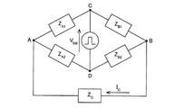
図10に、一般的なブリッジ回路の流れるコモンモード電流Icを示す。インピーダンスの比、すなわちZA1/ZA2とZB1/ZB2の値の相違が小さいほど、ブリッジ回路の平衡条件が満たされ、A点とB点の電位差が小さくなり、コモンモード電流が小さくなる。図9と図10を対比すると、インピーダンスZA1が浮遊容量Cmidに依存するインピーダンスに対応し、インピーダンスZA2が浮遊容量(2Cmid+3Cn+3Cp)に依存するインピーダンスに対応し、インピーダンスZB1が巻線MG_Aに依存するインピーダンスに対応し、インピーダンスZB2が巻線MG_Bと巻線MG_Cに依存するインピーダンスに対応する。また、インピーダンスZは、モータMGの対地浮遊容量Cmに依存したインピーダンスに対応する。一般的に、モータMGは三相対称な構造を有するので、巻線MG_A,MG_B,MG_Cの各々に依存するインピーダンスは等しい。したがって、インピーダンスZB2はインピーダンスZB1の半分となるので、図9においては、ZB1/ZB2が2/1である。このため、三相インバータ1の等価ブリッジ回路の平衡条件を満たすためには、ZA1/ZA2が2/1となるように調整するのが望ましい。 FIG. 10 shows a common mode current Ic flowing through a general bridge circuit. The smaller the impedance ratio, that is, the difference between the values of Z A1 / Z A2 and Z B1 / Z B2 , the more the equilibrium condition of the bridge circuit is satisfied, the smaller the potential difference between point A and point B, and the smaller the common mode current. . Comparing FIG. 9 and FIG. 10, the impedance Z A1 corresponds to the impedance depending on the stray capacitance Cmid, the impedance Z A2 corresponds to the impedance depending on the stray capacitance (2Cmid + 3Cn + 3Cp), and the impedance Z B1 depends on the winding MG_A. The impedance Z B2 corresponds to the impedance depending on the winding MG_B and the winding MG_C. The impedance Z C corresponds to the impedance that depends on ground stray capacitance Cm of the motor MG. In general, since the motor MG has a three-phase symmetrical structure, the impedance depending on each of the windings MG_A, MG_B, and MG_C is equal. Therefore, since the impedance Z B2 is half of the impedance Z B1 , in FIG. 9, Z B1 / Z B2 is 2/1. Therefore, in order to satisfy the equilibrium condition of the equivalent bridge circuit of the three-phase inverter 1, it is desirable to adjust Z A1 / Z A2 to be 2/1.

背景技術で説明した特開2009−273272号公報の技術では、等価ブリッジ回路の平衡条件を満たすために、浮遊容量Cp及び浮遊容量Cnが浮遊容量Cmidに対して十分に小さくなるように調整する(Cn,Cp<<Cmid)。例えば、特開2009−273272号公報の技術では、Cmid/Cn及びCmid/Cpの各々の容量比を100倍以上にする。そのような容量比を実現するためには、図2を参照すると、浮遊容量Cmidに対応した絶縁基板30,60の絶縁体層34,64の厚みを浮遊容量Cp,Cnに対応した絶縁基板40,50の絶縁体層44,54の厚みに対して十分に厚くしなければならない。あるいは、浮遊容量Cmidに対応した絶縁基板30,60の絶縁体層34,64の材料を浮遊容量Cp,Cnに対応した絶縁基板40,50の絶縁体層44,54の材料と異ならせなければならない。しかしながら、そのような設計は、以下の理由により容易なことではない。絶縁基板は、高電圧に耐えるための絶縁性能を保つ必要がある。絶縁基板の絶縁性能は厚みに比例するため、絶縁基板の厚みを100分の1に薄くすると、絶縁基板の絶縁性能を保つことが難しい。また、絶縁基板は、冷却器の冷却性能を阻害しないように低い熱抵抗である必要がある。絶縁基板の熱抵抗は厚みに比例するため、絶縁基板の厚みを100倍にすると、冷却器の冷却性能が阻害される。また、絶縁基板の材料は、絶縁性能、低熱抵抗及び機械的強度等を考慮すると、使用できる種類が限定される。このため、絶縁基板間で誘電率が100倍も異なる材料を使用することは、現実的に不可能である。   In the technique of Japanese Patent Laid-Open No. 2009-273272 described in the background art, the floating capacitance Cp and the floating capacitance Cn are adjusted to be sufficiently smaller than the floating capacitance Cmid in order to satisfy the equilibrium condition of the equivalent bridge circuit ( Cn, Cp << Cmid). For example, in the technique disclosed in Japanese Patent Application Laid-Open No. 2009-273272, the capacity ratio of each of Cmid / Cn and Cmid / Cp is set to 100 times or more. In order to realize such a capacitance ratio, referring to FIG. 2, the thickness of the insulating layers 34 and 64 of the insulating substrates 30 and 60 corresponding to the stray capacitance Cmid is set to the insulating substrate 40 corresponding to the stray capacitances Cp and Cn. , 50 of the insulating layers 44, 54 must be sufficiently thick. Alternatively, the material of the insulating layers 34 and 64 of the insulating substrates 30 and 60 corresponding to the stray capacitance Cmid must be different from the material of the insulating layers 44 and 54 of the insulating substrates 40 and 50 corresponding to the stray capacitances Cp and Cn. Don't be. However, such a design is not easy for the following reasons. The insulating substrate needs to maintain an insulating performance for withstanding a high voltage. Since the insulating performance of the insulating substrate is proportional to the thickness, it is difficult to maintain the insulating performance of the insulating substrate when the thickness of the insulating substrate is reduced to 1/100. The insulating substrate needs to have a low thermal resistance so as not to hinder the cooling performance of the cooler. Since the thermal resistance of the insulating substrate is proportional to the thickness, if the thickness of the insulating substrate is increased 100 times, the cooling performance of the cooler is hindered. Moreover, the material which can be used for the insulating substrate is limited in consideration of insulating performance, low thermal resistance, mechanical strength, and the like. For this reason, it is practically impossible to use materials having dielectric constants different by 100 times between insulating substrates.

以下、本明細書が開示する技術を説明する。本明細書は、製造が容易な構成の半導体モジュールを有するとともに、等価ブリッジ回路の平衡条件を満たすことができる三相インバータを開示する。また、本明細書は、そのような三相インバータ用の半導体モジュールを開示する。   The technology disclosed in this specification will be described below. The present specification discloses a three-phase inverter that has a semiconductor module that can be easily manufactured and that can satisfy the equilibrium condition of an equivalent bridge circuit. The present specification also discloses a semiconductor module for such a three-phase inverter.

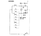
まず、本明細書で開示する技術が適用された三相インバータの回路構成は、図1に示す三相インバータ1と同一である。したがって、その説明を省略する。次に、図11に、本明細書が開示するU相レグ10Uを構成する両面冷却式のU相半導体モジュール200Uの要部断面図を模式的に示す。図2に示す従来のU相半導体モジュール100Uと共通する構成要素については共通の符号を付し、その説明を省略する。なお、他のV相レグ10V及びW相レグ10Wも共通形態の半導体モジュールを有する。   First, the circuit configuration of the three-phase inverter to which the technology disclosed in this specification is applied is the same as that of the three-phase inverter 1 shown in FIG. Therefore, the description is omitted. Next, FIG. 11 schematically shows a cross-sectional view of a main part of a double-sided cooling type U-phase semiconductor module 200U constituting the U-phase leg 10U disclosed in this specification. Constituent elements common to the conventional U-phase semiconductor module 100U shown in FIG. 2 are denoted by common reference numerals, and description thereof is omitted. The other V-phase leg 10V and W-phase leg 10W also have a common type semiconductor module.

図2の従来のU相半導体モジュール100Uと対比すると、図11のU相半導体モジュール200Uは、絶縁基板30,40,50,60の各々の絶縁体層34,44,54,64に中間導体層35,45,55,65が挿入されていることを特徴とする。ここで、絶縁体層34,44,54,64の各々に記載される添字「a」はチップ側であることを示し、添字「b」は冷却器側であることを示す。   Compared with the conventional U-phase semiconductor module 100U of FIG. 2, the U-phase semiconductor module 200U of FIG. 11 has an intermediate conductor layer on each of the insulator layers 34, 44, 54, 64 of the insulating substrates 30, 40, 50, 60. 35, 45, 55, and 65 are inserted. Here, the suffix “a” written on each of the insulator layers 34, 44, 54, 64 indicates the chip side, and the suffix “b” indicates the cooler side.

第1絶縁基板30は、第1スイッチング素子SW1及び第1ダイオードD1を含む半導体チップ2と冷却器20の間に設けられており、チップ側導体層32、チップ側絶縁体層34a、中間導体層35、冷却器側絶縁体層34b及び冷却器側導体層36を有する。チップ側導体層32、チップ側絶縁体層34a、中間導体層35、冷却器側絶縁体層34b及び冷却器側導体層36はこの順でチップ2から冷却器20に向けて積層しており、チップ側絶縁体層34aがチップ側導体層32と中間導体層35を絶縁しており、冷却器側絶縁体層34bが中間導体層35と冷却器側導体層36を絶縁する。   The first insulating substrate 30 is provided between the semiconductor chip 2 including the first switching element SW1 and the first diode D1 and the cooler 20, and includes a chip-side conductor layer 32, a chip-side insulator layer 34a, and an intermediate conductor layer. 35, a cooler side insulator layer 34b and a cooler side conductor layer 36 are provided. The chip side conductor layer 32, the chip side insulator layer 34a, the intermediate conductor layer 35, the cooler side insulator layer 34b, and the cooler side conductor layer 36 are laminated in this order from the chip 2 toward the cooler 20, The chip-side insulator layer 34a insulates the chip-side conductor layer 32 and the intermediate conductor layer 35, and the cooler-side insulator layer 34b insulates the intermediate conductor layer 35 and the cooler-side conductor layer 36.

第2絶縁基板40は、第1スイッチング素子SW1及び第1ダイオードD1を含む半導体チップ2と冷却器20の間に設けられており、チップ側導体層42、チップ側絶縁体層44a、中間導体層45、冷却器側絶縁体層44b及び冷却器側導体層46を有する。チップ側導体層42、チップ側絶縁体層44a、中間導体層45、冷却器側絶縁体層44b及び冷却器側導体層46はこの順でチップ2から冷却器20に向けて積層しており、チップ側絶縁体層44aがチップ側導体層42と中間導体層45を絶縁しており、冷却器側絶縁体層44bが中間導体層45と冷却器側導体層46を絶縁する。   The second insulating substrate 40 is provided between the semiconductor chip 2 including the first switching element SW1 and the first diode D1 and the cooler 20, and includes a chip-side conductor layer 42, a chip-side insulator layer 44a, and an intermediate conductor layer. 45, a cooler side insulator layer 44b and a cooler side conductor layer 46. The chip side conductor layer 42, the chip side insulator layer 44a, the intermediate conductor layer 45, the cooler side insulator layer 44b, and the cooler side conductor layer 46 are laminated in this order from the chip 2 toward the cooler 20, The chip-side insulator layer 44 a insulates the chip-side conductor layer 42 and the intermediate conductor layer 45, and the cooler-side insulator layer 44 b insulates the intermediate conductor layer 45 and the cooler-side conductor layer 46.

第3絶縁基板50は、第2スイッチング素子SW2及び第2ダイオードD2を含む半導体チップ4と冷却器20の間に設けられており、チップ側導体層52、チップ側絶縁体層54a、中間導体層55、冷却器側絶縁体層54b及び冷却器側導体層56を有する。チップ側導体層52、チップ側絶縁体層54a、中間導体層55、冷却器側絶縁体層54b及び冷却器側導体層56はこの順でチップ4から冷却器20に向けて積層しており、チップ側絶縁体層54aがチップ側導体層52と中間導体層55を絶縁しており、冷却器側絶縁体層54bが中間導体層55と冷却器側導体層56を絶縁する。   The third insulating substrate 50 is provided between the semiconductor chip 4 including the second switching element SW2 and the second diode D2 and the cooler 20, and includes a chip-side conductor layer 52, a chip-side insulator layer 54a, and an intermediate conductor layer. 55, a cooler-side insulator layer 54b and a cooler-side conductor layer 56. The chip side conductor layer 52, the chip side insulator layer 54a, the intermediate conductor layer 55, the cooler side insulator layer 54b, and the cooler side conductor layer 56 are laminated in this order from the chip 4 toward the cooler 20, The chip-side insulator layer 54a insulates the chip-side conductor layer 52 and the intermediate conductor layer 55, and the cooler-side insulator layer 54b insulates the intermediate conductor layer 55 and the cooler-side conductor layer 56.

第4絶縁基板60は、第2スイッチング素子SW2及び第2ダイオードD2を含む半導体チップ4と冷却器20の間に設けられており、チップ側導体層62、チップ側絶縁体層64a、中間導体層65、冷却器側絶縁体層64b及び冷却器側導体層66を有する。チップ側導体層62、チップ側絶縁体層64a、中間導体層65、冷却器側絶縁体層64b及び冷却器側導体層66はこの順でチップ4から冷却器20に向けて積層しており、チップ側絶縁体層64aがチップ側導体層62と中間導体層65を絶縁しており、冷却器側絶縁体層64bが中間導体層65と冷却器側導体層66を絶縁する。   The fourth insulating substrate 60 is provided between the semiconductor chip 4 including the second switching element SW2 and the second diode D2 and the cooler 20, and includes a chip-side conductor layer 62, a chip-side insulator layer 64a, and an intermediate conductor layer. 65, a cooler-side insulator layer 64b and a cooler-side conductor layer 66. The chip side conductor layer 62, the chip side insulator layer 64a, the intermediate conductor layer 65, the cooler side insulator layer 64b, and the cooler side conductor layer 66 are laminated in this order from the chip 4 to the cooler 20, The chip-side insulator layer 64a insulates the chip-side conductor layer 62 and the intermediate conductor layer 65, and the cooler-side insulator layer 64b insulates the intermediate conductor layer 65 and the cooler-side conductor layer 66.

第2絶縁基板40のチップ側導体層42が高電圧端子10Pに接続されており、第3絶縁基板50のチップ側導体層52が低電圧端子10Nに接続されている。第1絶縁基板30のチップ側導体層32と第4絶縁基板60のチップ側導体層62は、接続配線72を介して接続されており、U相中点MID_Uを構成する。さらに、第1絶縁基板30のチップ側導体層32と中間導体層35が接続配線82を介して接続されており、第1絶縁基板30の中間導体層35と第3絶縁基板50の中間導体層55が接続配線84を介して接続されており、第4絶縁基板60のチップ側導体層62と中間導体層65が接続配線86を介して接続されており、第4絶縁基板60の中間導体層65と第2絶縁基板40の中間導体層45が接続配線88を介して接続されている。   The chip side conductor layer 42 of the second insulating substrate 40 is connected to the high voltage terminal 10P, and the chip side conductor layer 52 of the third insulating substrate 50 is connected to the low voltage terminal 10N. The chip-side conductor layer 32 of the first insulating substrate 30 and the chip-side conductor layer 62 of the fourth insulating substrate 60 are connected via the connection wiring 72 and constitute the U-phase middle point MID_U. Further, the chip-side conductor layer 32 and the intermediate conductor layer 35 of the first insulating substrate 30 are connected via the connection wiring 82, and the intermediate conductor layer 35 of the first insulating substrate 30 and the intermediate conductor layer of the third insulating substrate 50 are connected. 55 is connected via a connection wiring 84, the chip-side conductor layer 62 of the fourth insulating substrate 60 and the intermediate conductor layer 65 are connected via a connection wiring 86, and the intermediate conductor layer of the fourth insulating substrate 60 is connected. 65 and the intermediate conductor layer 45 of the second insulating substrate 40 are connected via a connection wiring 88.

ここで、第1絶縁基板30のチップ側絶縁体層34a及び第2絶縁基板40のチップ側絶縁体層44aが特許請求の範囲に記載の第1高電圧側絶縁体層の一例であり、第1絶縁基板30の冷却器側絶縁体層34b及び第2絶縁基板40の冷却器側絶縁体層44bが特許請求の範囲に記載の第2高電圧側絶縁体層の一例であり、第1絶縁基板30の中間導体層35及び第2絶縁基板40の中間導体層45が特許請求の範囲に記載の高電圧側中間導体層の一例である。さらに、第3絶縁基板50のチップ側絶縁体層54a及び第4絶縁基板60のチップ側絶縁体層64aが特許請求の範囲に記載の第1低電圧側絶縁体層の一例であり、第3絶縁基板50の冷却器側絶縁体層54b及び第4絶縁基板60の冷却器側絶縁体層64bが特許請求の範囲に記載の第2低電圧側絶縁体層の一例であり、第3絶縁基板50の中間導体層55及び第4絶縁基板60の中間導体層65が特許請求の範囲に記載の低電圧側中間導体層の一例である。   Here, the chip-side insulator layer 34a of the first insulating substrate 30 and the chip-side insulator layer 44a of the second insulating substrate 40 are examples of the first high-voltage-side insulator layer described in the claims, The cooler-side insulator layer 34b of the first insulating substrate 30 and the cooler-side insulator layer 44b of the second insulating substrate 40 are examples of the second high-voltage-side insulator layer described in the claims. The intermediate conductor layer 35 of the substrate 30 and the intermediate conductor layer 45 of the second insulating substrate 40 are examples of the high voltage side intermediate conductor layer described in the claims. Furthermore, the chip-side insulator layer 54a of the third insulating substrate 50 and the chip-side insulator layer 64a of the fourth insulating substrate 60 are examples of the first low-voltage-side insulator layer described in the claims. The cooler-side insulator layer 54b of the insulating substrate 50 and the cooler-side insulator layer 64b of the fourth insulating substrate 60 are examples of the second low-voltage-side insulator layer recited in the claims, and the third insulating substrate 50 intermediate conductor layers 55 and the intermediate conductor layer 65 of the fourth insulating substrate 60 are examples of the low-voltage-side intermediate conductor layer described in the claims.

図12に、U相半導体モジュール200Uの等価回路を示す。また、図13に、図12の等価回路を整理したU相半導体モジュール200Uの等価回路を示す。図12及び図13では、絶縁基板30,40,50,60の各々に存在する浮遊容量を破線で示す。U相半導体モジュール200Uでは、絶縁基板30,40,50,60の各々の絶縁体層34,44,54,64に中間導体層35,45,55,65が挿入されているので、絶縁基板30,40,50,60の各々に2つの浮遊容量が存在する。ここで、浮遊容量に記載される添字「a」はチップ側絶縁体層34a,44a,54a,64aに対応する浮遊容量であることを示し、添字「b」は冷却器側絶縁体層34b,44b,54b,64bに対応する浮遊容量であることを示す。   FIG. 12 shows an equivalent circuit of the U-phase semiconductor module 200U. FIG. 13 shows an equivalent circuit of the U-phase semiconductor module 200U in which the equivalent circuit of FIG. 12 is arranged. 12 and 13, the stray capacitance existing in each of the insulating substrates 30, 40, 50 and 60 is indicated by a broken line. In the U-phase semiconductor module 200U, the intermediate conductor layers 35, 45, 55, 65 are inserted into the insulator layers 34, 44, 54, 64 of the insulating substrates 30, 40, 50, 60, respectively. , 40, 50, 60 each have two stray capacitances. Here, the subscript “a” written in the stray capacitance indicates a stray capacitance corresponding to the chip-side insulator layers 34a, 44a, 54a, 64a, and the subscript “b” indicates the cooler-side insulator layer 34b, The stray capacitances corresponding to 44b, 54b, and 64b are indicated.

図12に示されるように、第1絶縁基板30では、中間導体層35が接続配線82を介してU相中点MID_Uに接続する。このため、第1絶縁基板30のチップ側絶縁体層34aに対応する浮遊容量Cmid_Uaは消失する。第4絶縁基板60では、中間導体層65が接続配線86を介してU相中点MID_Uに接続する。このため、第4絶縁基板60のチップ側絶縁体層64aに対応する浮遊容量Cmid_Uaは消失する。また、第2絶縁基板40では、中間導体層45が接続配線72,86,88を介してU相中点MID_Uに接続する。このため、第2絶縁基板40では、チップ側絶縁体層44aに対応する浮遊容量Cp_Uaがチップ側導体層42とU相中点MID_Uの間に存在することになり、冷却器側絶縁体層44bに対応する浮遊容量Cp_UbがU相中点MID_Uと冷却器20の間に存在することになる。第3絶縁基板50では、中間導体層55が接続配線82,84を介してU相中点MID_Uに接続する。このため、第3絶縁基板50では、チップ側絶縁体層54aに対応する浮遊容量Cn_Uaがチップ側導体層52とU相中点MID_Uの間に存在することになり、冷却器側絶縁体層54bに対応する浮遊容量Cn_UbがU相中点MID_Uと冷却器20の間に存在することになる。このため、図12の等価回路は、図13のU相半導体モジュール200Uの等価回路に整理することができる。   As shown in FIG. 12, in the first insulating substrate 30, the intermediate conductor layer 35 is connected to the U-phase middle point MID_U through the connection wiring 82. For this reason, the stray capacitance Cmid_Ua corresponding to the chip-side insulator layer 34a of the first insulating substrate 30 disappears. In the fourth insulating substrate 60, the intermediate conductor layer 65 is connected to the U-phase middle point MID_U via the connection wiring 86. For this reason, the stray capacitance Cmid_Ua corresponding to the chip-side insulator layer 64a of the fourth insulating substrate 60 disappears. In the second insulating substrate 40, the intermediate conductor layer 45 is connected to the U-phase middle point MID_U via the connection wires 72, 86, 88. Therefore, in the second insulating substrate 40, the stray capacitance Cp_Ua corresponding to the chip-side insulator layer 44a exists between the chip-side conductor layer 42 and the U-phase middle point MID_U, and the cooler-side insulator layer 44b. The stray capacitance Cp_Ub corresponding to is present between the U-phase midpoint MID_U and the cooler 20. In the third insulating substrate 50, the intermediate conductor layer 55 is connected to the U-phase middle point MID_U via the connection wires 82 and 84. Therefore, in the third insulating substrate 50, the stray capacitance Cn_Ua corresponding to the chip-side insulator layer 54a exists between the chip-side conductor layer 52 and the U-phase middle point MID_U, and the cooler-side insulator layer 54b. The stray capacitance Cn_Ub corresponding to is present between the U-phase midpoint MID_U and the cooler 20. For this reason, the equivalent circuit of FIG. 12 can be organized into an equivalent circuit of the U-phase semiconductor module 200U of FIG.

上記したように、レグ10U,10V,10Wを構成する半導体モジュールの各々は共通形態である。このため、図12及び図13で説明したU相レグ10UのU相半導体モジュール100Uと同様に、他のレグ10V,10Wの半導体モジュールの各々にも浮遊容量が存在する。図14に、三相インバータ1を構成する全てのレグ10U,10V,10Wの半導体モジュールに存在する浮遊容量を示すとともに、三相インバータ1が動作したときの等価回路を示す。図14では、U相レグ10Uがスイッチング動作を行う場合を例示する。なお、モータMGを構成する巻線MG_U,MG_V,MG_Wの各々の他端は、対地浮遊容量Cmを介して接地GNDされている。なお、モータの対地浮遊容量は、この例に限らず、モータの種類等に応じて異なる態様で存在し得る。後述するように、本明細書で開示する技術は、モータの対地浮遊容量の態様に制限されずに、効果を発揮することができる。換言すれば、本明細書で開示する技術は、様々な種類のモータに対して適用可能である。   As described above, each of the semiconductor modules constituting the legs 10U, 10V, and 10W has a common form. Therefore, like the U-phase semiconductor module 100U of the U-phase leg 10U described with reference to FIGS. 12 and 13, stray capacitance also exists in each of the other leg 10V, 10W semiconductor modules. FIG. 14 shows stray capacitances present in all the semiconductor modules of the legs 10U, 10V, and 10W constituting the three-phase inverter 1, and an equivalent circuit when the three-phase inverter 1 operates. FIG. 14 illustrates a case where the U-phase leg 10U performs a switching operation. Note that the other end of each of the windings MG_U, MG_V, MG_W constituting the motor MG is grounded via a ground floating capacitance Cm. The ground stray capacitance of the motor is not limited to this example, and may exist in different modes depending on the type of the motor. As will be described later, the technique disclosed in the present specification is not limited to the aspect of the ground floating capacitance of the motor, and can exert an effect. In other words, the technology disclosed in this specification can be applied to various types of motors.

図14において、短絡により消失する浮遊容量を削除すると、図15の等価回路に整理することができる。上記したように、レグ10U,10V,10Wを構成する半導体モジュールの各々は共通形態である。即ち、レグ10U,10V,10Wを構成する半導体モジュール間において、対応する絶縁基板30,40,50,60が共通形態である。このため、レグ10U,10V,10Wの各々の浮遊容量Cn_Ub,Cn_Vb,Cn_Wbは浮遊容量Cnbとして共通表記することができ、浮遊容量Cp_Ub,Cp_Vb,Cp_Wbは浮遊容量Cpbとして共通表記することができ、容量Cmid_Ub,Cmid_Vb,Cmid_Wbは浮遊容量Cmidbとして共通表記することができる。このため、図15に示す等価回路は、図16に示す等価回路に整理することができる。   In FIG. 14, if the stray capacitance that disappears due to a short circuit is deleted, the equivalent circuit of FIG. 15 can be arranged. As described above, each of the semiconductor modules constituting the legs 10U, 10V, and 10W has a common form. That is, the corresponding insulating substrates 30, 40, 50, 60 are common among the semiconductor modules constituting the legs 10 U, 10 V, 10 W. Therefore, the stray capacitances Cn_Ub, Cn_Vb, and Cn_Wb of the legs 10U, 10V, and 10W can be commonly expressed as the stray capacitance Cnb, and the stray capacitances Cp_Ub, Cp_Vb, and Cp_Wb can be commonly expressed as the stray capacitance Cpb. The capacitors Cmid_Ub, Cmid_Vb, and Cmid_Wb can be commonly expressed as stray capacitance Cmidb. For this reason, the equivalent circuit shown in FIG. 15 can be organized into the equivalent circuit shown in FIG.

図16では、U相レグ10Uがスイッチング動作を行う場合を例示する。しかしながら、上記図7〜図9で説明したように、この例でも、V相レグ10Vがスイッチング動作を行う場合、W相レグ10Wがスイッチング動作を行う場合のいずれも、同様の手順により、図16と同様の等価回路が作成される。また、スイッチング動作を行わないレグの各々において、上アームと下アームのいずれか一方が導通状態(短絡)であり他方が非導通状態(開放)である限りにおいて、上アームと下アームの導通状態(短絡)と非導通状態(開放)がどのように選択されていても、同様の手順により、図16と同様の等価回路が作成される。したがって、スイッチング動作を行うレグの中点をMID_Aと表記し、その他のレグの中点をそれぞれMID_B,MID_Cと表記し、スイッチング動作を行うレグの中点に接続される巻線をMG_Aと表記し、その他のレグの中点に接続される巻線をそれぞれMG_B,MG_Cと表記すると、図16の等価回路は図17の等価回路に書き換えられる。図17は、三相インバータ1が動作したときの三相インバータ1の等価回路とみなすことができる。   FIG. 16 illustrates a case where the U-phase leg 10U performs a switching operation. However, as described above with reference to FIGS. 7 to 9, also in this example, when the V-phase leg 10 </ b> V performs the switching operation and when the W-phase leg 10 </ b> W performs the switching operation, the same procedure is used. An equivalent circuit similar to is created. Also, in each leg that does not perform the switching operation, the upper arm and the lower arm are in the conductive state as long as either the upper arm or the lower arm is in the conductive state (short circuit) and the other is in the nonconductive state (open). An equivalent circuit similar to that in FIG. 16 is created by the same procedure regardless of how the (short-circuit) and non-conduction states (open) are selected. Therefore, the midpoint of the leg that performs the switching operation is denoted as MID_A, the midpoints of the other legs are denoted as MID_B and MID_C, respectively, and the winding connected to the midpoint of the leg that performs the switching operation is denoted as MG_A. When the windings connected to the midpoints of the other legs are denoted as MG_B and MG_C, respectively, the equivalent circuit of FIG. 16 is rewritten to the equivalent circuit of FIG. FIG. 17 can be regarded as an equivalent circuit of the three-phase inverter 1 when the three-phase inverter 1 operates.

図17の等価回路を図10の一般的なブリッジ回路と対比すると、インピーダンスZA1が浮遊容量(Cmidb+Cnb+Cpb)に依存するインピーダンスに対応し、インピーダンスZA2が浮遊容量(2Cmidb+2Cnb+2Cpb)に依存するインピーダンスに対応し、インピーダンスZB1が巻線MG_Aに依存するインピーダンスに対応し、インピーダンスZB2が巻線MG_Bと巻線MG_Cに依存するインピーダンスに対応する。また、インピーダンスZは、モータMGの対地浮遊容量Cmに依存したインピーダンスに対応する。ここで、図17においては、ZA1/ZA2が2/1であり、ZB1/ZB2も2/1である。このため、三相インバータ1の等価ブリッジ回路は、平衡条件を満たすように構成されている。 When the equivalent circuit of FIG. 17 is compared with the general bridge circuit of FIG. 10, the impedance Z A1 corresponds to the impedance depending on the stray capacitance (Cmidb + Cnb + Cpb), and the impedance Z A2 corresponds to the impedance depending on the stray capacitance (2Cmidb + 2Cnb + 2Cpb). The impedance Z B1 corresponds to the impedance dependent on the winding MG_A, and the impedance Z B2 corresponds to the impedance dependent on the winding MG_B and the winding MG_C. The impedance Z C corresponds to the impedance that depends on ground stray capacitance Cm of the motor MG. Here, in FIG. 17, Z A1 / Z A2 is 2/1, and Z B1 / Z B2 is also 2/1. For this reason, the equivalent bridge circuit of the three-phase inverter 1 is configured to satisfy the equilibrium condition.

このように、本明細書で開示する三相インバータ1の等価ブリッジ回路は、それ自体が平衡条件を満たすように半導体モジュールに存在する浮遊容量が配分されている。上記したように、三相インバータ1のレグ10U,10V,10Wを構成する半導体モジュールの各々は共通形態である。このため、三相インバータ1の等価ブリッジ回路のインピーダンスの比、すなわちZA1/ZA2とZB1/ZB2の値が極めて良く一致し、コモンモード電流が極めて低減される。なお、三相インバータ1において、レグ10U,10V,10Wを構成する半導体モジュールの各々は共通形態である必要があるが、各レグ10U,10V,10Wを構成する絶縁基板30,40,50,60の各々は共通形態でなくても、絶縁体層34,44,54,64に中間導体層35,45,55,65が挿入されるとともに、その中間導体層35,45,55,65が中点MID_U,MID_V,MID_Wに短絡していれば、平衡条件を満たすような浮遊容量の配分効果によって、コモンモード電流は低下することができる。 As described above, the equivalent bridge circuit of the three-phase inverter 1 disclosed in this specification is allocated with the stray capacitance existing in the semiconductor module so as to satisfy the equilibrium condition itself. As described above, each of the semiconductor modules constituting the legs 10U, 10V, 10W of the three-phase inverter 1 has a common form. Therefore, the impedance ratio of the equivalent bridge circuit of the three-phase inverter 1, that is, the values of Z A1 / Z A2 and Z B1 / Z B2 agree very well, and the common mode current is extremely reduced. In the three-phase inverter 1, each of the semiconductor modules constituting the legs 10U, 10V, 10W needs to have a common form, but the insulating substrates 30, 40, 50, 60 constituting each leg 10U, 10V, 10W are required. Are not in common form, the intermediate conductor layers 35, 45, 55, 65 are inserted into the insulator layers 34, 44, 54, 64, and the intermediate conductor layers 35, 45, 55, 65 are in the middle. If short-circuited to the points MID_U, MID_V, and MID_W, the common mode current can be reduced by the stray capacitance distribution effect that satisfies the equilibrium condition.

上記したように、背景技術で説明した特開2009−273272号公報の技術では、絶縁基板間で容量比を大きくするために、絶縁基板間で厚みを異ならせたり、絶縁基板間で材料を異ならせたりしなければならない。このため、設計の自由度が制限されてしまう。一方、本明細書で開示する三相インバータ1は、平衡条件を満たすような浮遊容量の配分効果を有しているので、そのような設計の自由度の制限を緩和することができる。例えば、半導体モジュールの各々が共通形態であれば、等価ブリッジ回路の平衡条件が満たされるので、半導体モジュールの絶縁基板の厚み及び材料を自由に設計することができる。   As described above, in the technique of Japanese Patent Application Laid-Open No. 2009-273272 described in the background art, in order to increase the capacitance ratio between the insulating substrates, the thickness is different between the insulating substrates, or the materials are different between the insulating substrates. You have to let them. For this reason, the freedom degree of design will be restrict | limited. On the other hand, the three-phase inverter 1 disclosed in the present specification has an effect of stray capacitance distribution that satisfies the equilibrium condition, and therefore, it is possible to relax the restriction on the degree of freedom of design. For example, if each of the semiconductor modules has a common form, the equilibrium condition of the equivalent bridge circuit is satisfied, so that the thickness and material of the insulating substrate of the semiconductor module can be freely designed.

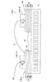
上記では、本明細書で開示する技術を両面冷却式のU相半導体モジュール200Uを例に説明したが、本明細書で開示する技術は、片面冷却式の半導体モジュールを備える三相インバータにも適用できる。図18に、本明細書が開示するU相レグ10Uを構成する片面冷却式のU相半導体モジュール300Uの要部断面図を模式的に示す。図11に示す両面冷却式のU相半導体モジュール200Uと共通する構成要素については共通の符号を付し、その説明を省略する。なお、他のV相レグ10V及びW相レグ10Wも共通形態の半導体モジュールを有する。   In the above, the technology disclosed in this specification has been described by taking the double-sided cooling U-phase semiconductor module 200U as an example. However, the technology disclosed in this specification can also be applied to a three-phase inverter including a single-sided cooling type semiconductor module. it can. FIG. 18 schematically shows a cross-sectional view of a main part of a single-sided cooling U-phase semiconductor module 300U constituting the U-phase leg 10U disclosed in the present specification. Constituent elements common to the double-sided cooling U-phase semiconductor module 200U shown in FIG. The other V-phase leg 10V and W-phase leg 10W also have a common type semiconductor module.

このような片面冷却式の半導体モジュールで構成される三相インバータ1の等価ブリッジ回路は、図17の等価ブリッジ回路から浮遊容量Cp_Ua及び浮遊容量Cpbを除去したものに対応する。この場合も同様に、三相インバータ1の等価ブリッジ回路が平衡条件を満たすように構成されており、コモンモード電流が低下する。   The equivalent bridge circuit of the three-phase inverter 1 constituted by such a single-sided cooling type semiconductor module corresponds to a circuit obtained by removing the stray capacitance Cp_Ua and the stray capacitance Cpb from the equivalent bridge circuit of FIG. In this case as well, the equivalent bridge circuit of the three-phase inverter 1 is configured to satisfy the equilibrium condition, and the common mode current is reduced.

上記したように、本明細書で開示される技術では、絶縁基板30,40,50,60の中間導体層35,45,55,65が中点MID_U,MID_V,MID_Wに短絡することを特徴とする。上記では、短絡する様子が接続配線82,84,86,88を利用して表記されているが、この接続配線82,84,86,88は、短絡している様子を示すことを目的として記載されているのであって、短絡させるためには、様々な形態が採用し得る。例えば、第1絶縁基板30と第3絶縁基板50は、チップ側絶縁体層34a,54a、中間導体層35,55、冷却器側絶縁体層34b,54b及び冷却器側導体層36,56が一体の積層体で構成されていてもよい。この場合、接続配線84は不要である。同様に、第2絶縁基板40と第4絶縁基板60は、チップ側絶縁体層44a,64a、中間導体層45,65、冷却器側絶縁体層44b,64b及び冷却器側導体層46,66が一体の積層体で構成されていてもよい。この場合、接続配線88は不要である。   As described above, the technology disclosed in this specification is characterized in that the intermediate conductor layers 35, 45, 55, 65 of the insulating substrates 30, 40, 50, 60 are short-circuited to the midpoints MID_U, MID_V, MID_W. To do. In the above, the state of short-circuiting is described using the connection wirings 82, 84, 86, and 88, but the connection wirings 82, 84, 86, and 88 are described for the purpose of showing the state of short-circuiting. In order to short-circuit, various forms can be adopted. For example, the first insulating substrate 30 and the third insulating substrate 50 include chip-side insulator layers 34a and 54a, intermediate conductor layers 35 and 55, cooler-side insulator layers 34b and 54b, and cooler-side conductor layers 36 and 56. You may be comprised with the integral laminated body. In this case, the connection wiring 84 is unnecessary. Similarly, the second insulating substrate 40 and the fourth insulating substrate 60 include chip-side insulator layers 44a and 64a, intermediate conductor layers 45 and 65, cooler-side insulator layers 44b and 64b, and cooler-side conductor layers 46 and 66. May be composed of an integral laminate. In this case, the connection wiring 88 is unnecessary.

以上、本発明の実施例について詳細に説明したが、これらは例示に過ぎず、特許請求の範囲を限定するものではない。特許請求の範囲に記載の技術には、以上に例示した具体例を様々に変形、変更したものが含まれる。本明細書または図面に説明した技術要素は、単独であるいは各種の組合せによって技術的有用性を発揮するものであり、出願時の請求項に記載の組合せに限定されるものではない。また、本明細書または図面に例示した技術は複数目的を同時に達成するものであり、そのうちの一つの目的を達成すること自体で技術的有用性を持つものである。   As mentioned above, although the Example of this invention was described in detail, these are only illustrations and do not limit a claim. The technology described in the claims includes various modifications and changes of the specific examples illustrated above. The technical elements described in this specification or the drawings exhibit technical usefulness alone or in various combinations, and are not limited to the combinations described in the claims at the time of filing. In addition, the technology illustrated in the present specification or the drawings achieves a plurality of objects at the same time, and has technical utility by achieving one of the objects.

1:三相インバータ
2:半導体チップ
4:半導体チップ
10N:低電圧端子
10P:高電圧端子
10U:U相レグ
10V:V相レグ
10W:W相レグ
20:冷却器
30:第1絶縁基板
40:第2絶縁基板
50:第3絶縁基板
60:第4絶縁基板
32,42,52,62:チップ側導体層
34a,44a,54a,64a:チップ側絶縁体層
34b,44b,54b,64b:冷却器側絶縁体層
35,45,55,65:中間導体層
36,46,56,66:冷却器側導体層
72,82,84,86,88:接続配線
SW1−6:スイッチング素子
D1−6:ダイオード
MG:モータ
1: three-phase inverter 2: semiconductor chip 4: semiconductor chip 10N: low voltage terminal 10P: high voltage terminal 10U: U phase leg 10V: V phase leg 10W: W phase leg 20: cooler 30: first insulating substrate 40: Second insulating substrate 50: Third insulating substrate 60: Fourth insulating substrates 32, 42, 52, 62: Chip side conductor layers 34a, 44a, 54a, 64a: Chip side insulating layers 34b, 44b, 54b, 64b: Cooling Appliance side insulator layers 35, 45, 55, 65: Intermediate conductor layers 36, 46, 56, 66: Cooler side conductor layers 72, 82, 84, 86, 88: Connection wiring SW1-6: Switching element D1-6 : Diode MG: Motor

Claims (3)

三相インバータであって、
冷却器と、
前記冷却器で冷却して用いられるとともに、U相、V相及びW相を構成する半導体モジュールと、
高電圧端子と、
低電圧端子と、を備えており、
前記半導体モジュールは、各相において、
前記高電圧端子に接続する高電圧側スイッチング素子と、
前記低電圧端子に接続する低電圧側スイッチング素子と、
前記高電圧側スイッチング素子と前記冷却器の間に設けられる高電圧側絶縁基板と、
前記低電圧側スイッチング素子と前記冷却器の間に設けられる低電圧側絶縁基板と、を有しており、
前記高電圧側スイッチング素子と前記低電圧側スイッチング素子は、前記高電圧端子と前記低電圧端子の間に直列に接続されており、
前記高電圧側絶縁基板は、
前記高電圧側スイッチング素子側に配置されている第1高電圧側絶縁体層と、
前記冷却器側に配置されている第2高電圧側絶縁体層と、
前記第1高電圧側絶縁体層と前記第2高電圧側絶縁体層の間に設けられている高電圧側中間導体層と、を含み、
前記低電圧側絶縁基板は、
前記低電圧側スイッチング素子側に配置されている第1低電圧側絶縁体層と、
前記冷却器側に配置されている第2低電圧側絶縁体層と、
前記第1低電圧側絶縁体層と前記第2低電圧側絶縁体層の間に設けられている低電圧側中間導体層と、を含み、
前記高電圧側中間導体層及び前記低電圧側中間導体層が、前記高電圧側スイッチング素子と前記低電圧側スイッチング素子の中点に接続するように構成されている、三相インバータ。
A three-phase inverter,
A cooler,
A semiconductor module which is used after being cooled by the cooler, and which constitutes a U phase, a V phase and a W phase,
A high voltage terminal;
A low voltage terminal, and
The semiconductor module, in each phase,
A high voltage side switching element connected to the high voltage terminal;
A low voltage side switching element connected to the low voltage terminal;
A high voltage side insulating substrate provided between the high voltage side switching element and the cooler;
A low voltage side insulating substrate provided between the low voltage side switching element and the cooler,
The high voltage side switching element and the low voltage side switching element are connected in series between the high voltage terminal and the low voltage terminal,
The high-voltage side insulating substrate is
A first high voltage side insulator layer disposed on the high voltage side switching element side;
A second high voltage side insulator layer disposed on the cooler side;
A high voltage side intermediate conductor layer provided between the first high voltage side insulator layer and the second high voltage side insulator layer,
The low voltage side insulating substrate is:
A first low voltage side insulator layer disposed on the low voltage side switching element side;
A second low voltage side insulator layer disposed on the cooler side;
A low voltage side intermediate conductor layer provided between the first low voltage side insulator layer and the second low voltage side insulator layer,
The three-phase inverter, wherein the high voltage side intermediate conductor layer and the low voltage side intermediate conductor layer are configured to be connected to a midpoint between the high voltage side switching element and the low voltage side switching element.
前記高電圧側絶縁基板は、各相間において共通形態であり、
前記低電圧側絶縁基板は、各相間において共通形態である、請求項1に記載の三相インバータ。
The high voltage side insulating substrate is in a common form between the phases,
The three-phase inverter according to claim 1, wherein the low-voltage side insulating substrate has a common form between the phases.
冷却器で冷却して用いられる三相インバータ用の半導体モジュールであって、
前記三相インバータの高電圧端子に接続する高電圧側スイッチング素子と、
前記三相インバータの低電圧端子に接続する低電圧側スイッチング素子と、
前記高電圧側スイッチング素子と前記冷却器の間に設けられる高電圧側絶縁基板と、
前記低電圧側スイッチング素子と前記冷却器の間に設けられる低電圧側絶縁基板と、を備えており、
前記高電圧側スイッチング素子と前記低電圧側スイッチング素子は、前記高電圧端子と前記低電圧端子の間に直列に接続されるように構成されており、
前記高電圧側絶縁基板は、
前記高電圧側スイッチング素子側に配置されている第1高電圧側絶縁体層と、
前記冷却器側に配置されている第2高電圧側絶縁体層と、
前記第1高電圧側絶縁体層と前記第2高電圧側絶縁体層の間に設けられている高電圧側中間導体層と、を有しており、
前記低電圧側絶縁基板は、
前記低電圧側スイッチング素子側に配置されている第1低電圧側絶縁体層と、
前記冷却器側に配置されている第2低電圧側絶縁体層と、
前記第1低電圧側絶縁体層と前記第2低電圧側絶縁体層の間に設けられている低電圧側中間導体層と、を有しており、
前記高電圧側中間導体層及び前記低電圧側中間導体層が、前記高電圧側スイッチング素子と前記低電圧側スイッチング素子の中点に接続するように構成されている、半導体モジュール。
A semiconductor module for a three-phase inverter that is used after being cooled by a cooler,
A high voltage side switching element connected to a high voltage terminal of the three-phase inverter;
A low voltage side switching element connected to a low voltage terminal of the three-phase inverter;
A high voltage side insulating substrate provided between the high voltage side switching element and the cooler;
A low voltage side insulating substrate provided between the low voltage side switching element and the cooler,
The high voltage side switching element and the low voltage side switching element are configured to be connected in series between the high voltage terminal and the low voltage terminal,
The high-voltage side insulating substrate is
A first high voltage side insulator layer disposed on the high voltage side switching element side;
A second high voltage side insulator layer disposed on the cooler side;
A high voltage side intermediate conductor layer provided between the first high voltage side insulator layer and the second high voltage side insulator layer;
The low voltage side insulating substrate is:
A first low voltage side insulator layer disposed on the low voltage side switching element side;
A second low voltage side insulator layer disposed on the cooler side;
A low voltage side intermediate conductor layer provided between the first low voltage side insulator layer and the second low voltage side insulator layer;
The semiconductor module, wherein the high voltage side intermediate conductor layer and the low voltage side intermediate conductor layer are configured to be connected to a midpoint between the high voltage side switching element and the low voltage side switching element.
JP2016046175A 2016-03-09 2016-03-09 Three-phase inverter and semiconductor module therefor Pending JP2017163709A (en)

Priority Applications (1)

Application Number Priority Date Filing Date Title
JP2016046175A JP2017163709A (en) 2016-03-09 2016-03-09 Three-phase inverter and semiconductor module therefor

Applications Claiming Priority (1)

Application Number Priority Date Filing Date Title
JP2016046175A JP2017163709A (en) 2016-03-09 2016-03-09 Three-phase inverter and semiconductor module therefor

Publications (1)

Publication Number Publication Date
JP2017163709A true JP2017163709A (en) 2017-09-14

Family

ID=59858084

Family Applications (1)

Application Number Title Priority Date Filing Date
JP2016046175A Pending JP2017163709A (en) 2016-03-09 2016-03-09 Three-phase inverter and semiconductor module therefor

Country Status (1)

Country Link
JP (1) JP2017163709A (en)

Cited By (3)

* Cited by examiner, † Cited by third party
Publication number Priority date Publication date Assignee Title
WO2022107809A1 (en) * 2020-11-19 2022-05-27 サンデン・アドバンストテクノロジー株式会社 Power conversion device
WO2023090263A1 (en) * 2021-11-17 2023-05-25 サンデン株式会社 Power conversion device and method for manufacturing same
JP7496434B2 (en) 2020-11-19 2024-06-06 サンデン株式会社 Power Conversion Equipment

Cited By (3)

* Cited by examiner, † Cited by third party
Publication number Priority date Publication date Assignee Title
WO2022107809A1 (en) * 2020-11-19 2022-05-27 サンデン・アドバンストテクノロジー株式会社 Power conversion device
JP7496434B2 (en) 2020-11-19 2024-06-06 サンデン株式会社 Power Conversion Equipment
WO2023090263A1 (en) * 2021-11-17 2023-05-25 サンデン株式会社 Power conversion device and method for manufacturing same

Similar Documents

Publication Publication Date Title
JP3633432B2 (en) Semiconductor device and power conversion device
JP4603956B2 (en) Power converter
US10411589B2 (en) Power conversion apparatus and power semiconductor module
JP5644943B2 (en) Semiconductor module, upper and lower arm kit and 3-level inverter
US10600716B2 (en) Power converter
JP3621659B2 (en) Power conversion system
JP2014533487A (en) Power converter based on H-bridge
KR101686313B1 (en) Power module and 3-level power conversion device using same
JP5851267B2 (en) Inverter and vehicle control device
JP6196853B2 (en) 3 level converter half bridge
JP6962945B2 (en) Power semiconductor module and power converter using it
JP6053668B2 (en) Semiconductor module and power conversion device
JP2014217270A (en) Half bridge for 3-level power conversion device
WO2017141407A1 (en) Power semiconductor module
JP5241421B2 (en) Power converter
JP2017163709A (en) Three-phase inverter and semiconductor module therefor
JP2012222892A (en) Power converter
JP2017143647A (en) Power converter device
JPH10304680A (en) Power converter
JP5341824B2 (en) Semiconductor device
JP2009268165A (en) Inverter module
JP2015133281A (en) Terminal block, and power conversion system with the same
JPWO2018109884A1 (en) Power converter
JP2020092518A (en) Electric power conversion system
JP2013038848A (en) Semiconductor device