JP2017163197A - 電力増幅回路 - Google Patents
電力増幅回路 Download PDFInfo
- Publication number
- JP2017163197A JP2017163197A JP2016043312A JP2016043312A JP2017163197A JP 2017163197 A JP2017163197 A JP 2017163197A JP 2016043312 A JP2016043312 A JP 2016043312A JP 2016043312 A JP2016043312 A JP 2016043312A JP 2017163197 A JP2017163197 A JP 2017163197A
- Authority
- JP
- Japan
- Prior art keywords
- transistor
- circuit
- input
- power amplifier
- gate
- Prior art date
- Legal status (The legal status is an assumption and is not a legal conclusion. Google has not performed a legal analysis and makes no representation as to the accuracy of the status listed.)
- Pending
Links
- 238000006386 neutralization reaction Methods 0.000 claims abstract description 38
- 230000003071 parasitic effect Effects 0.000 claims description 50
- 239000003990 capacitor Substances 0.000 claims description 39
- 230000003472 neutralizing effect Effects 0.000 claims description 7
- 238000010586 diagram Methods 0.000 description 17
- 238000006880 cross-coupling reaction Methods 0.000 description 9
- 238000000034 method Methods 0.000 description 9
- 230000003321 amplification Effects 0.000 description 8
- 238000003199 nucleic acid amplification method Methods 0.000 description 8
- 230000008569 process Effects 0.000 description 8
- 230000007423 decrease Effects 0.000 description 7
- 238000004519 manufacturing process Methods 0.000 description 5
- 238000004891 communication Methods 0.000 description 4
- 230000008878 coupling Effects 0.000 description 4
- 238000010168 coupling process Methods 0.000 description 4
- 238000005859 coupling reaction Methods 0.000 description 4
- 230000000694 effects Effects 0.000 description 4
- 238000002955 isolation Methods 0.000 description 4
- 238000013461 design Methods 0.000 description 3
- 230000006872 improvement Effects 0.000 description 3
- 239000000203 mixture Substances 0.000 description 3
- 239000004065 semiconductor Substances 0.000 description 3
- 239000002184 metal Substances 0.000 description 2
- 230000010355 oscillation Effects 0.000 description 2
- 230000015556 catabolic process Effects 0.000 description 1
- 230000008859 change Effects 0.000 description 1
- 230000000295 complement effect Effects 0.000 description 1
- 230000002079 cooperative effect Effects 0.000 description 1
- 238000011161 development Methods 0.000 description 1
- 230000005672 electromagnetic field Effects 0.000 description 1
- 238000005516 engineering process Methods 0.000 description 1
- 239000000284 extract Substances 0.000 description 1
- 230000010354 integration Effects 0.000 description 1
- 239000000463 material Substances 0.000 description 1
- 238000012545 processing Methods 0.000 description 1
Images


Classifications
-
- H—ELECTRICITY
- H03—ELECTRONIC CIRCUITRY
- H03F—AMPLIFIERS
- H03F1/00—Details of amplifiers with only discharge tubes, only semiconductor devices or only unspecified devices as amplifying elements
- H03F1/02—Modifications of amplifiers to raise the efficiency, e.g. gliding Class A stages, use of an auxiliary oscillation
- H03F1/0205—Modifications of amplifiers to raise the efficiency, e.g. gliding Class A stages, use of an auxiliary oscillation in transistor amplifiers
-
- H—ELECTRICITY
- H03—ELECTRONIC CIRCUITRY
- H03F—AMPLIFIERS
- H03F3/00—Amplifiers with only discharge tubes or only semiconductor devices as amplifying elements
- H03F3/20—Power amplifiers, e.g. Class B amplifiers, Class C amplifiers
- H03F3/21—Power amplifiers, e.g. Class B amplifiers, Class C amplifiers with semiconductor devices only
- H03F3/211—Power amplifiers, e.g. Class B amplifiers, Class C amplifiers with semiconductor devices only using a combination of several amplifiers
-
- H—ELECTRICITY
- H03—ELECTRONIC CIRCUITRY
- H03F—AMPLIFIERS
- H03F1/00—Details of amplifiers with only discharge tubes, only semiconductor devices or only unspecified devices as amplifying elements
- H03F1/08—Modifications of amplifiers to reduce detrimental influences of internal impedances of amplifying elements
- H03F1/14—Modifications of amplifiers to reduce detrimental influences of internal impedances of amplifying elements by use of neutralising means
-
- H—ELECTRICITY
- H03—ELECTRONIC CIRCUITRY
- H03F—AMPLIFIERS
- H03F3/00—Amplifiers with only discharge tubes or only semiconductor devices as amplifying elements
- H03F3/189—High-frequency amplifiers, e.g. radio frequency amplifiers
- H03F3/19—High-frequency amplifiers, e.g. radio frequency amplifiers with semiconductor devices only
- H03F3/193—High-frequency amplifiers, e.g. radio frequency amplifiers with semiconductor devices only with field-effect devices
-
- H—ELECTRICITY
- H03—ELECTRONIC CIRCUITRY
- H03F—AMPLIFIERS
- H03F3/00—Amplifiers with only discharge tubes or only semiconductor devices as amplifying elements
- H03F3/20—Power amplifiers, e.g. Class B amplifiers, Class C amplifiers
- H03F3/21—Power amplifiers, e.g. Class B amplifiers, Class C amplifiers with semiconductor devices only
-
- H—ELECTRICITY
- H03—ELECTRONIC CIRCUITRY
- H03F—AMPLIFIERS
- H03F3/00—Amplifiers with only discharge tubes or only semiconductor devices as amplifying elements
- H03F3/45—Differential amplifiers
- H03F3/45071—Differential amplifiers with semiconductor devices only
- H03F3/45076—Differential amplifiers with semiconductor devices only characterised by the way of implementation of the active amplifying circuit in the differential amplifier
- H03F3/45179—Differential amplifiers with semiconductor devices only characterised by the way of implementation of the active amplifying circuit in the differential amplifier using MOSFET transistors as the active amplifying circuit
-
- H—ELECTRICITY
- H03—ELECTRONIC CIRCUITRY
- H03F—AMPLIFIERS
- H03F2200/00—Indexing scheme relating to amplifiers
- H03F2200/21—Bias resistors are added at the input of an amplifier
-
- H—ELECTRICITY
- H03—ELECTRONIC CIRCUITRY
- H03F—AMPLIFIERS
- H03F2200/00—Indexing scheme relating to amplifiers
- H03F2200/267—A capacitor based passive circuit, e.g. filter, being used in an amplifying circuit
-
- H—ELECTRICITY
- H03—ELECTRONIC CIRCUITRY
- H03F—AMPLIFIERS
- H03F2200/00—Indexing scheme relating to amplifiers
- H03F2200/451—Indexing scheme relating to amplifiers the amplifier being a radio frequency amplifier
-
- H—ELECTRICITY
- H03—ELECTRONIC CIRCUITRY
- H03F—AMPLIFIERS
- H03F2203/00—Indexing scheme relating to amplifiers with only discharge tubes or only semiconductor devices as amplifying elements covered by H03F3/00
- H03F2203/45—Indexing scheme relating to differential amplifiers
- H03F2203/45031—Indexing scheme relating to differential amplifiers the differential amplifier amplifying transistors are compositions of multiple transistors
-
- H—ELECTRICITY
- H03—ELECTRONIC CIRCUITRY
- H03F—AMPLIFIERS
- H03F2203/00—Indexing scheme relating to amplifiers with only discharge tubes or only semiconductor devices as amplifying elements covered by H03F3/00
- H03F2203/45—Indexing scheme relating to differential amplifiers
- H03F2203/45034—One or more added reactive elements, capacitive or inductive elements, to the amplifying transistors in the differential amplifier
-
- H—ELECTRICITY
- H03—ELECTRONIC CIRCUITRY
- H03F—AMPLIFIERS
- H03F2203/00—Indexing scheme relating to amplifiers with only discharge tubes or only semiconductor devices as amplifying elements covered by H03F3/00
- H03F2203/45—Indexing scheme relating to differential amplifiers
- H03F2203/45244—Indexing scheme relating to differential amplifiers the differential amplifier contains one or more explicit bias circuits, e.g. to bias the tail current sources, to bias the load transistors
-
- H—ELECTRICITY
- H03—ELECTRONIC CIRCUITRY
- H03F—AMPLIFIERS
- H03F2203/00—Indexing scheme relating to amplifiers with only discharge tubes or only semiconductor devices as amplifying elements covered by H03F3/00
- H03F2203/45—Indexing scheme relating to differential amplifiers
- H03F2203/45318—Indexing scheme relating to differential amplifiers the AAC comprising a cross coupling circuit, e.g. two extra transistors cross coupled
-
- H—ELECTRICITY
- H03—ELECTRONIC CIRCUITRY
- H03F—AMPLIFIERS
- H03F2203/00—Indexing scheme relating to amplifiers with only discharge tubes or only semiconductor devices as amplifying elements covered by H03F3/00
- H03F2203/45—Indexing scheme relating to differential amplifiers
- H03F2203/45394—Indexing scheme relating to differential amplifiers the AAC of the dif amp comprising FETs whose sources are not coupled, i.e. the AAC being a pseudo-differential amplifier
Landscapes
- Engineering & Computer Science (AREA)
- Power Engineering (AREA)
- Amplifiers (AREA)
Abstract
Description
まず、本開示に至る経緯について説明する。本開示は、100GHzを超える高周波帯で動作する電力増幅回路に関する。
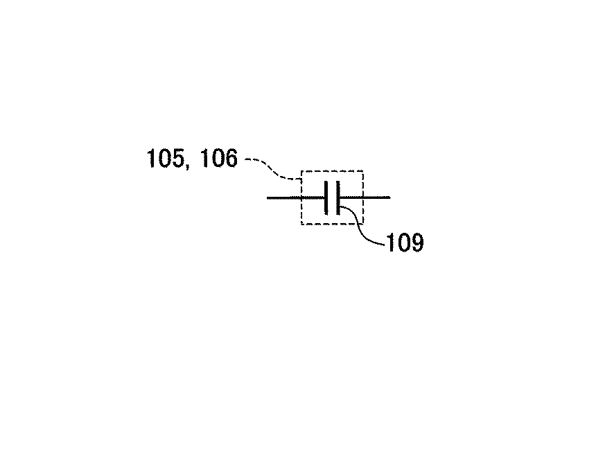
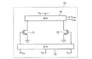
図3は、本開示の実施の形態1に係る電力増幅回路100の構成例を示す回路図である。電力増幅回路100は、入力トランジスタ101、102と、カスコードトランジスタ103、104と、中和回路105、106と、入力回路107と、出力回路108とを有する。
図7は、本開示の実施の形態2に係る電力増幅回路200の構成例を示す回路図である。なお、図7において、図3に示した構成と同様の構成については、同一の符番を付し説明を省略する。
図9は、本開示の実施の形態3に係る電力増幅回路300を示す図である。なお、図9において、図7に示した構成と同様の構成については、同一の符番を付し説明を省略する。
実施の形態3では、カスコードトランジスタを多段構成する例について説明した。カスコードトランジスタを多段構成にすると、カスコードトランジスタの耐圧を超える電圧がかかり、カスコードトランジスタが故障してしまう場合がある。実施の形態4では、カスコードトランジスタのゲートに供給するバイアス電圧を調整することにより、カスコードトランジスタのソースの電位を調整し、カスコードトランジスタにかかる電圧を所望の電圧に抑えることができる構成について説明する。
11、12、101、102 入力トランジスタ
13、107 入力回路
14、108 出力回路
15、16 クロスカップリングキャパシタ
17、18、110、401−1〜401−N、402−1〜402−N 抵抗
103、103−1〜103−N、104、104−1〜104−N カスコードトランジスタ
105、106 中和回路
109、403−1〜403−N、404−1〜404−N キャパシタ
201、201−1〜201−N、202、202−1〜202−N インダクタ
405−1〜405−N、406−1〜406−N コンパレータ
Claims (5)
- 第1位相を有する第1入力信号と前記第1位相を反転させた第2位相を有する第2入力信号が入力される入力回路と、
ソースに第1電圧が供給され、前記入力回路から前記第1入力信号をゲートで受ける第1トランジスタと、
ソースに前記第1電圧が供給され、前記入力回路から前記第2入力信号をゲートで受ける第2トランジスタと、
前記第2トランジスタのゲートと前記第1トランジスタのドレインとの間に接続され、寄生素子を中和する第1中和回路と、
前記第1トランジスタのゲートと前記第2トランジスタのドレインとの間に接続され、寄生素子を中和する第2中和回路と、
前記第1トランジスタのドレインに縦続接続されるN個(Nは1以上の整数)の第3トランジスタと、
前記第2トランジスタのドレインに縦続接続されるN個の第4トランジスタと、
N番目の前記第3トランジスタのドレインとN番目の前記第4トランジスタのドレインに接続され、第3位相を有する第1出力信号と前記第3位相を反転させた第4位相を有する第2出力信号とを出力する出力回路と、
を備える電力増幅回路。 - 前記第1中和回路および前記第2中和回路は、それぞれ、キャパシタを有する、
請求項1に記載の電力増幅回路。 - 前記第1中和回路および前記第2中和回路は、それぞれ、前記キャパシタに直列に接続する抵抗を有する、
請求項2に記載の電力増幅回路。 - 前記N個の第3トランジスタに接続されるN個の第1インダクタと、
前記N個の第4トランジスタに接続されるN個の第2インダクタと、
を更に備え、
前記N個の第3トランジスタのうちi番目(iは1以上N以下の整数)の第3トランジスタのゲートには、互いに異なるN通りのバイアス電圧のうち第iのバイアス電圧が供給され、
前記N個の第4トランジスタのうち前記i番目の第3トランジスタと対を為すi番目の第4トランジスタのゲートには、前記第iのバイアス電圧が供給され、
前記N個の第1インダクタのうちi番目の第1インダクタは、前記i番目の第3トランジスタのゲートに一方の端子が接続され、他方の端子から前記第iのバイアス電圧が供給され、
前記N個の第2インダクタのうちi番目の第2インダクタは、前記i番目の第4トランジスタのゲートに一方の端子が接続され、他方の端子から前記第iのバイアス電圧が供給される、
請求項1から3のいずれか一項に記載の電力増幅回路。 - 前記N個の第3トランジスタのうちi番目(iは1以上N以下の整数)の第3トランジスタのゲートには、互いに異なるN通りのバイアス電圧のうち第iのバイアス電圧が供給され、
前記N個の第4トランジスタうち前記i番目の第3トランジスタと対を為すi番目の第4トランジスタのゲートには、前記第iのバイアス電圧が供給され、
第1および第2の入力端子と1つの出力端子とを有し、前記i番目の第3トランジスタ及び前記i番目の第4トランジスタの少なくとも1つのトランジスタに前記第iのバイアス電圧を供給するコンパレータと、
第1および第2の接続端子を有し、前記第1の接続端子が前記第1の入力端子に接続され、前記第2の接続端子に前記第1電圧が供給されるキャパシタと、
前記第1の入力端子と、前記少なくとも1つのトランジスタのソースとの間に接続される抵抗と、
を更に備え、
前記コンパレータは、前記第2の入力端子に参照電圧が供給され、前記少なくとも1つのトランジスタのソースの電圧と前記第1電圧との差が前記参照電圧と等しくなるように、前記第iのバイアス電圧を制御する、
請求項1から3のいずれか一項に記載の電力増幅回路。
Priority Applications (3)
| Application Number | Priority Date | Filing Date | Title |
|---|---|---|---|
| JP2016043312A JP2017163197A (ja) | 2016-03-07 | 2016-03-07 | 電力増幅回路 |
| CN201611195475.6A CN107171648A (zh) | 2016-03-07 | 2016-12-21 | 功率放大电路 |
| US15/409,506 US9935583B2 (en) | 2016-03-07 | 2017-01-18 | Power amplifier circuit |
Applications Claiming Priority (1)
| Application Number | Priority Date | Filing Date | Title |
|---|---|---|---|
| JP2016043312A JP2017163197A (ja) | 2016-03-07 | 2016-03-07 | 電力増幅回路 |
Publications (1)
| Publication Number | Publication Date |
|---|---|
| JP2017163197A true JP2017163197A (ja) | 2017-09-14 |
Family
ID=59722920
Family Applications (1)
| Application Number | Title | Priority Date | Filing Date |
|---|---|---|---|
| JP2016043312A Pending JP2017163197A (ja) | 2016-03-07 | 2016-03-07 | 電力増幅回路 |
Country Status (3)
| Country | Link |
|---|---|
| US (1) | US9935583B2 (ja) |
| JP (1) | JP2017163197A (ja) |
| CN (1) | CN107171648A (ja) |
Cited By (1)
| Publication number | Priority date | Publication date | Assignee | Title |
|---|---|---|---|---|
| WO2022180762A1 (ja) * | 2021-02-26 | 2022-09-01 | 三菱電機株式会社 | 差動増幅装置 |
Families Citing this family (5)
| Publication number | Priority date | Publication date | Assignee | Title |
|---|---|---|---|---|
| WO2019221175A1 (ja) * | 2018-05-17 | 2019-11-21 | 株式会社村田製作所 | 増幅回路 |
| CN109660213A (zh) * | 2018-12-19 | 2019-04-19 | 上海秦芯信息科技有限公司 | 一种应用于5g毫米波基站的功率放大器 |
| CN109995357A (zh) * | 2019-04-23 | 2019-07-09 | 北京中科格励微科技有限公司 | 线性隔离器 |
| GB2607005A (en) * | 2021-05-14 | 2022-11-30 | Nordic Semiconductor Asa | Rf amplifier with a cascode device |
| US20230238881A1 (en) * | 2022-01-27 | 2023-07-27 | Qualcomm Incorporated | Radio frequency (rf) power amplifier with transformer for improved output power, wideband, and spurious rejection |
Citations (5)
| Publication number | Priority date | Publication date | Assignee | Title |
|---|---|---|---|---|
| JPS60105307A (ja) * | 1984-09-28 | 1985-06-10 | Hitachi Ltd | 増幅回路 |
| JP2003532321A (ja) * | 2000-04-06 | 2003-10-28 | ケイデンス・デザイン・システムズ・インコーポレーテッド | Mosカスコード回路中のホット・エレクトロン・デグラデーション効果を低減するための限圧バイアス回路 |
| US20060057990A1 (en) * | 2004-09-10 | 2006-03-16 | Arya Behzad | Gain boosting RF gain stage with cross-coupled capacitors |
| US20130063210A1 (en) * | 2011-09-09 | 2013-03-14 | Texas Instruments Incorporated | High speed amplifier |
| JP2014175675A (ja) * | 2013-03-05 | 2014-09-22 | Panasonic Corp | 高周波増幅回路、無線通信装置、及び高周波増幅回路の制御方法 |
Family Cites Families (8)
| Publication number | Priority date | Publication date | Assignee | Title |
|---|---|---|---|---|
| US7415286B2 (en) * | 2005-04-08 | 2008-08-19 | Broadcom Corporation | Gain boosting for local oscillation distribution circuitry |
| US7639079B2 (en) * | 2007-02-09 | 2009-12-29 | Agere Systems Inc. | Techniques for designing wide band low noise amplifiers |
| JP5228017B2 (ja) | 2010-09-16 | 2013-07-03 | 株式会社東芝 | 高周波差動増幅回路 |
| US20150236748A1 (en) * | 2013-03-14 | 2015-08-20 | Peregrine Semiconductor Corporation | Devices and Methods for Duplexer Loss Reduction |
| US9294042B2 (en) * | 2013-03-15 | 2016-03-22 | Rf Micro Devices (Cayman Islands), Ltd. | Power amplifier system with supply modulation mitigation circuitry and methods |
| US9490759B2 (en) * | 2014-05-27 | 2016-11-08 | Avago Technologies General Ip (Singapore) Pte. Ltd. | Neutralization of parasitic capacitance using MOS device |
| US9413309B1 (en) * | 2015-03-25 | 2016-08-09 | Analog Devices Global | Apparatus and methods for a cascode amplifier topology for millimeter-wave power application |
| CN104779931A (zh) * | 2015-04-09 | 2015-07-15 | 西安电子科技大学 | 一种高增益线性度的可变增益放大器 |
-
2016
- 2016-03-07 JP JP2016043312A patent/JP2017163197A/ja active Pending
- 2016-12-21 CN CN201611195475.6A patent/CN107171648A/zh active Pending
-
2017
- 2017-01-18 US US15/409,506 patent/US9935583B2/en not_active Expired - Fee Related
Patent Citations (5)
| Publication number | Priority date | Publication date | Assignee | Title |
|---|---|---|---|---|
| JPS60105307A (ja) * | 1984-09-28 | 1985-06-10 | Hitachi Ltd | 増幅回路 |
| JP2003532321A (ja) * | 2000-04-06 | 2003-10-28 | ケイデンス・デザイン・システムズ・インコーポレーテッド | Mosカスコード回路中のホット・エレクトロン・デグラデーション効果を低減するための限圧バイアス回路 |
| US20060057990A1 (en) * | 2004-09-10 | 2006-03-16 | Arya Behzad | Gain boosting RF gain stage with cross-coupled capacitors |
| US20130063210A1 (en) * | 2011-09-09 | 2013-03-14 | Texas Instruments Incorporated | High speed amplifier |
| JP2014175675A (ja) * | 2013-03-05 | 2014-09-22 | Panasonic Corp | 高周波増幅回路、無線通信装置、及び高周波増幅回路の制御方法 |
Cited By (1)
| Publication number | Priority date | Publication date | Assignee | Title |
|---|---|---|---|---|
| WO2022180762A1 (ja) * | 2021-02-26 | 2022-09-01 | 三菱電機株式会社 | 差動増幅装置 |
Also Published As
| Publication number | Publication date |
|---|---|
| US9935583B2 (en) | 2018-04-03 |
| CN107171648A (zh) | 2017-09-15 |
| US20170257067A1 (en) | 2017-09-07 |
Similar Documents
| Publication | Publication Date | Title |
|---|---|---|
| JP2017163197A (ja) | 電力増幅回路 | |
| JP4305472B2 (ja) | 差動増幅器 | |
| DE102016105181B4 (de) | Vorrichtungen und Verfahren für eine Kaskodenverstärkertopologie für Millimeterwellenleistungsanwendung | |
| US9960948B2 (en) | Method and apparatus of an input resistance of a passive mixer to broaden the input matching bandwidth of a common source/gate LNA | |
| US8305151B2 (en) | Resonance type oscillation circuit and semiconductor device | |
| US7663441B2 (en) | Low noise amplifier | |
| US9397714B1 (en) | Radio frequency receiver circuit and the inductor-coupling single-ended input differential-output low-noise amplifier thereof | |
| US10985710B2 (en) | Power amplifier module | |
| JP2014175675A (ja) | 高周波増幅回路、無線通信装置、及び高周波増幅回路の制御方法 | |
| Ben Hammadi et al. | RF and microwave reconfigurable bandpass filter design using optimized active inductor circuit | |
| KR100860794B1 (ko) | 이중대역 저잡음 증폭기 | |
| US10164586B2 (en) | Impedance-matching circuit | |
| US20110148526A1 (en) | Low noise amplifier with variable frequency response | |
| WO2013053661A1 (en) | A low-noise amplifier circuit | |
| US10911007B2 (en) | High-frequency amplifier circuitry and semiconductor device | |
| CN108880481B (zh) | 低噪放大器、用于低噪放大器的接收器和方法 | |
| KR20210130923A (ko) | 트랜지스터 기생성분 매칭을 이용한 저잡음 증폭기 | |
| CN111903054B (zh) | 单端转差分放大器和射频接收机 | |
| Gee et al. | CMOS integrated LC RF bandpass filter with transformer-coupled Q-enhancement and optimized linearity | |
| EP3748848B1 (en) | Variable inductor circuit | |
| Muhamad et al. | Linearity improvement of differential CMOS low noise amplifier | |
| KR102010154B1 (ko) | 무선 주파수 증폭기 및 무선 주파수 증폭기를 이용한 집적회로 | |
| Ghaly et al. | A 9 mw wideband 60 GHz LNA with 3.55 dB NF | |
| Pepe et al. | Millimeter-wave high-Q active inductor in 65nm CMOS | |
| Meharde et al. | Low Voltage CMOS Active Inductor with Bandwidth and Linearity Improvement |
Legal Events
| Date | Code | Title | Description |
|---|---|---|---|
| A621 | Written request for application examination |
Free format text: JAPANESE INTERMEDIATE CODE: A621 Effective date: 20180927 |
|
| A977 | Report on retrieval |
Free format text: JAPANESE INTERMEDIATE CODE: A971007 Effective date: 20190529 |
|
| A131 | Notification of reasons for refusal |
Free format text: JAPANESE INTERMEDIATE CODE: A131 Effective date: 20190611 |
|
| RD02 | Notification of acceptance of power of attorney |
Free format text: JAPANESE INTERMEDIATE CODE: A7422 Effective date: 20190718 |
|
| RD04 | Notification of resignation of power of attorney |
Free format text: JAPANESE INTERMEDIATE CODE: A7424 Effective date: 20191121 |
|
| A02 | Decision of refusal |
Free format text: JAPANESE INTERMEDIATE CODE: A02 Effective date: 20191217 |