JP2017162032A - Display device - Google Patents
Display device Download PDFInfo
- Publication number
- JP2017162032A JP2017162032A JP2016043910A JP2016043910A JP2017162032A JP 2017162032 A JP2017162032 A JP 2017162032A JP 2016043910 A JP2016043910 A JP 2016043910A JP 2016043910 A JP2016043910 A JP 2016043910A JP 2017162032 A JP2017162032 A JP 2017162032A
- Authority
- JP
- Japan
- Prior art keywords
- electrode
- display device
- electrodes
- touch sensor
- detection
- Prior art date
- Legal status (The legal status is an assumption and is not a legal conclusion. Google has not performed a legal analysis and makes no representation as to the accuracy of the status listed.)
- Pending
Links
Images


Classifications
-
- G—PHYSICS
- G06—COMPUTING; CALCULATING OR COUNTING
- G06F—ELECTRIC DIGITAL DATA PROCESSING
- G06F3/00—Input arrangements for transferring data to be processed into a form capable of being handled by the computer; Output arrangements for transferring data from processing unit to output unit, e.g. interface arrangements
- G06F3/01—Input arrangements or combined input and output arrangements for interaction between user and computer
- G06F3/03—Arrangements for converting the position or the displacement of a member into a coded form
- G06F3/041—Digitisers, e.g. for touch screens or touch pads, characterised by the transducing means
- G06F3/044—Digitisers, e.g. for touch screens or touch pads, characterised by the transducing means by capacitive means
- G06F3/0448—Details of the electrode shape, e.g. for enhancing the detection of touches, for generating specific electric field shapes, for enhancing display quality
-
- G—PHYSICS
- G06—COMPUTING; CALCULATING OR COUNTING
- G06F—ELECTRIC DIGITAL DATA PROCESSING
- G06F3/00—Input arrangements for transferring data to be processed into a form capable of being handled by the computer; Output arrangements for transferring data from processing unit to output unit, e.g. interface arrangements
- G06F3/01—Input arrangements or combined input and output arrangements for interaction between user and computer
- G06F3/03—Arrangements for converting the position or the displacement of a member into a coded form
- G06F3/041—Digitisers, e.g. for touch screens or touch pads, characterised by the transducing means
- G06F3/0412—Digitisers structurally integrated in a display
-
- G—PHYSICS
- G06—COMPUTING; CALCULATING OR COUNTING
- G06F—ELECTRIC DIGITAL DATA PROCESSING
- G06F3/00—Input arrangements for transferring data to be processed into a form capable of being handled by the computer; Output arrangements for transferring data from processing unit to output unit, e.g. interface arrangements
- G06F3/01—Input arrangements or combined input and output arrangements for interaction between user and computer
- G06F3/03—Arrangements for converting the position or the displacement of a member into a coded form
- G06F3/041—Digitisers, e.g. for touch screens or touch pads, characterised by the transducing means
- G06F3/044—Digitisers, e.g. for touch screens or touch pads, characterised by the transducing means by capacitive means
- G06F3/0443—Digitisers, e.g. for touch screens or touch pads, characterised by the transducing means by capacitive means using a single layer of sensing electrodes
-
- G—PHYSICS
- G06—COMPUTING; CALCULATING OR COUNTING
- G06F—ELECTRIC DIGITAL DATA PROCESSING
- G06F3/00—Input arrangements for transferring data to be processed into a form capable of being handled by the computer; Output arrangements for transferring data from processing unit to output unit, e.g. interface arrangements
- G06F3/01—Input arrangements or combined input and output arrangements for interaction between user and computer
- G06F3/03—Arrangements for converting the position or the displacement of a member into a coded form
- G06F3/041—Digitisers, e.g. for touch screens or touch pads, characterised by the transducing means
- G06F3/044—Digitisers, e.g. for touch screens or touch pads, characterised by the transducing means by capacitive means
- G06F3/0446—Digitisers, e.g. for touch screens or touch pads, characterised by the transducing means by capacitive means using a grid-like structure of electrodes in at least two directions, e.g. using row and column electrodes
-
- H—ELECTRICITY
- H10—SEMICONDUCTOR DEVICES; ELECTRIC SOLID-STATE DEVICES NOT OTHERWISE PROVIDED FOR
- H10K—ORGANIC ELECTRIC SOLID-STATE DEVICES
- H10K59/00—Integrated devices, or assemblies of multiple devices, comprising at least one organic light-emitting element covered by group H10K50/00
- H10K59/40—OLEDs integrated with touch screens
-
- G—PHYSICS
- G06—COMPUTING; CALCULATING OR COUNTING
- G06F—ELECTRIC DIGITAL DATA PROCESSING
- G06F2203/00—Indexing scheme relating to G06F3/00 - G06F3/048
- G06F2203/041—Indexing scheme relating to G06F3/041 - G06F3/045
- G06F2203/04103—Manufacturing, i.e. details related to manufacturing processes specially suited for touch sensitive devices
-
- G—PHYSICS
- G06—COMPUTING; CALCULATING OR COUNTING
- G06F—ELECTRIC DIGITAL DATA PROCESSING
- G06F2203/00—Indexing scheme relating to G06F3/00 - G06F3/048
- G06F2203/041—Indexing scheme relating to G06F3/041 - G06F3/045
- G06F2203/04111—Cross over in capacitive digitiser, i.e. details of structures for connecting electrodes of the sensing pattern where the connections cross each other, e.g. bridge structures comprising an insulating layer, or vias through substrate
-
- H—ELECTRICITY
- H10—SEMICONDUCTOR DEVICES; ELECTRIC SOLID-STATE DEVICES NOT OTHERWISE PROVIDED FOR
- H10K—ORGANIC ELECTRIC SOLID-STATE DEVICES
- H10K59/00—Integrated devices, or assemblies of multiple devices, comprising at least one organic light-emitting element covered by group H10K50/00
- H10K59/10—OLED displays
- H10K59/12—Active-matrix OLED [AMOLED] displays
- H10K59/131—Interconnections, e.g. wiring lines or terminals
Landscapes
- Engineering & Computer Science (AREA)
- General Engineering & Computer Science (AREA)
- Theoretical Computer Science (AREA)
- Human Computer Interaction (AREA)
- Physics & Mathematics (AREA)
- General Physics & Mathematics (AREA)
- Quality & Reliability (AREA)
- Electroluminescent Light Sources (AREA)
- Position Input By Displaying (AREA)
Abstract
Description
本発明は表示装置に関する。特に有機EL素子を形成した表示領域上にタッチセンサを搭載した表示装置に関する。 The present invention relates to a display device. In particular, the present invention relates to a display device in which a touch sensor is mounted on a display region in which an organic EL element is formed.
モバイル機器用の表示装置は、薄型化、軽量化が要求されており、この観点で液晶表示装置と有機EL表示装置とを比較すると、バックライトを必要としない点において、有機EL表示装置が有利だと考えられる。また、近年ではフレキシブル基板上に画素駆動回路及び有機EL素子を形成する技術の開発が進んでおり、従来のガラス基板を用いたものに比べ、より薄く、軽いディスプレイが実現されている。このような流れにおいて、表示デバイス以外の部材、例えばタッチセンサ、偏光板等についても薄型化が望まれており、特にタッチセンサを別部材として表示装置上に貼り付け実装すると、厚さが増大してしまうために、表示装置への内蔵化が求められている。 Display devices for mobile devices are required to be thinner and lighter. From this point of view, when comparing a liquid crystal display device and an organic EL display device, an organic EL display device is advantageous in that a backlight is not required. It is thought that. In recent years, development of a technique for forming a pixel driving circuit and an organic EL element on a flexible substrate has been progressed, and a thinner and lighter display is realized as compared with a conventional glass substrate. In such a flow, it is desired to reduce the thickness of members other than the display device, such as touch sensors and polarizing plates. Especially, when the touch sensor is attached and mounted on the display device as a separate member, the thickness increases. Therefore, it is required to be built in a display device.
有機EL表示装置にタッチセンサを内蔵させる方式に関しては、例えば、特許文献1に開示されている。この発明では、有機EL素子を形成する電極の一方を帯状にし、タッチセンサの電極として使用することが示されている。一方、特許文献2には、タッチセンサと表示装置との間に低誘電率の層を設ける構成が開示されている。
A method for incorporating a touch sensor in an organic EL display device is disclosed in
有機EL表示装置にタッチセンサを内蔵させることにより、新たな課題が発生する。その1つとして、タッチセンサの電極と有機EL素子との間の距離が接近することにより、有機EL素子を駆動する画素駆動回路への信号入力および回路動作に起因したノイズが大きくなることがある。これによりタッチセンサのS/N比が低下し、センシングの性能が悪化してしまう。有機EL層は複数の層による積層構造になっているが、最上層にはカソードもしくはアノードの導電膜が一様に形成されるのが一般的で、この導電膜との間に働く寄生容量が増大する。 A new problem arises by incorporating a touch sensor in an organic EL display device. For example, when the distance between the electrode of the touch sensor and the organic EL element approaches, noise due to signal input to the pixel driving circuit that drives the organic EL element and circuit operation may increase. . As a result, the S / N ratio of the touch sensor decreases, and the sensing performance deteriorates. The organic EL layer has a laminated structure composed of a plurality of layers, but the cathode or anode conductive film is generally formed uniformly on the top layer, and the parasitic capacitance acting between this conductive film is Increase.
寄生容量の増大は、時定数の増加、検出信号レベルの低下に繋がるため、検出時間増大、S/N比低下によりセンシングの性能が悪化してしまう。特許文献2のように、低誘電率の層を挟むことで寄生容量を削減する構成も考えられるが、薄型化について課題が残るとともに部材の追加が必要になる。 Since the increase in parasitic capacitance leads to an increase in time constant and a decrease in detection signal level, sensing performance deteriorates due to an increase in detection time and a decrease in S / N ratio. As in Patent Document 2, a configuration in which parasitic capacitance is reduced by sandwiching a low dielectric constant layer is also conceivable. However, there remains a problem with thinning, and an additional member is required.
本発明は、上記課題を鑑み、タッチセンサの電極構造を改良することにより寄生容量を好適に削減する構成について考案し、当該構成を有する表示装置を提供するものである。 In view of the above problems, the present invention devised a configuration that suitably reduces parasitic capacitance by improving the electrode structure of a touch sensor, and provides a display device having the configuration.
本発明の表示装置は、発光素子およびトランジスタを有する複数の画素がマトリクス状に配置された表示領域と、前記表示領域上に設けられたタッチセンサと、を有し、前記タッチセンサは、複数の第1電極と、複数の第2電極と、を有し、前記複数の第1電極は、環状形状の電極が連なった形状を有することを特徴とする。 The display device of the present invention includes a display area in which a plurality of pixels each having a light emitting element and a transistor are arranged in a matrix, and a touch sensor provided on the display area. It has a 1st electrode and a some 2nd electrode, The said some 1st electrode has the shape where the cyclic | annular electrode was continued, It is characterized by the above-mentioned.
上記の手段により、タッチセンサ電極の寄生容量を低減させることができ、センシング性能を向上させることができる。 By the above means, the parasitic capacitance of the touch sensor electrode can be reduced, and the sensing performance can be improved.
以下に、本発明の各実施の形態について、図面を参照しつつ説明する。図面は、説明をより明確にするため、実際の態様に比べ、各部の幅、厚さ、形状等について模式的に表される場合があるが、あくまで一例であって、本発明の解釈を限定するものではない。また、本明細書と各図において、既出の図に関して前述したものと同様の要素には、同一の符号を付して詳細な説明を適宜省略することがある。 Hereinafter, embodiments of the present invention will be described with reference to the drawings. In order to make the explanation clearer, the drawings may be schematically represented with respect to the width, thickness, shape, and the like of each part as compared to the actual embodiment, but are merely examples and limit the interpretation of the present invention. Not what you want. In addition, in the present specification and each drawing, elements similar to those described above with reference to the previous drawings may be denoted by the same reference numerals and detailed description thereof may be omitted as appropriate.
また、本発明において、ある構造体の「上に」他の構造体を配置する態様を表現するにあたり、単に「上に」と表記する場合、特に断りの無い限りは、ある構造体に接するように、直上に他の構造体を配置する場合と、ある構造体の上方に、さらに他の構造体を介して他の構造体を配置する場合との両方を含むものとする。 Further, in the present invention, in expressing the mode of disposing another structure “on” a certain structure, when simply describing “on top”, unless otherwise noted, the structure touches a certain structure. In addition, both the case where another structure is arranged directly above and the case where another structure is arranged via another structure above a certain structure are included.
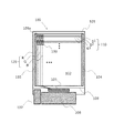
図1は本発明の表示装置の構成例である。表示装置100は、基板101上に、表示領域102、及び走査線駆動回路103、104がそれぞれ形成されており、ドライバIC105、表示用FPC(フレキシブルプリント基板)106、及びタッチ用FPC107が接続されている。ドライバIC105は、図1においては基板101上に実装されているが、表示用FPC106上に実装されていてもよい。また、表示領域102を覆うように、対向基板108が設けられていてもよい。表示領域102には、行方向(図1中、水平方向)に走る走査線、列方向(図1中、垂直方向)に走る映像信号線がそれぞれ複数本配置されている。走査線と映像信号線の交点には、副画素109aが配置されている。副画素109aは、それぞれ異なる色に発光する発光素子を有し、複数が集まって1画素109(図1中、点線枠で表示)を形成することでフルカラー表示を行う。この例では、走査線110は画素1行当たり3本(g1、g2、g3)配置され、映像信号線120は画素1列あたり3本(R、G、B)配置されている。また図示されていないが、表示領域102内には発光素子に一定電圧を供給するための電源線等の配線も存在する。各副画素109aには、ドライバIC105から映像信号線120を介して供給される信号に応じた輝度で発光するように、発光素子の輝度制御を行う画素回路が配置される。
FIG. 1 is a structural example of a display device of the present invention. In the
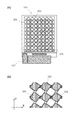
表示装置100は、表示機能に加えてタッチセンサを備える。図1においては、特に表示機能に関する説明を行うためタッチセンサは省略されていたが、図2(A)に示すように、発光素子の上層、つまり発光素子よりも表示面側に配置される。タッチセンサは、例えば2種類の電極より形成され、一方が行方向に走る駆動電極201、他方が列方向に走る検出電極202である。
The
図2(B)に、図2(A)における点線枠210の拡大図を示す。図2(B)において、X方向が行方向、Y方向が列方向に該当する。駆動電極201及び検出電極202は、表示装置100の表示領域上に設けられるため、ITO(インジウムスズ酸化物)、IZO(インジウム亜鉛酸化物)等の透明導電膜により形成される。透明導電膜を形成する他の材料としては、Agナノワイヤ等が考えられる。Agナノワイヤは、溶媒中に微細な繊維状のAgを分散させた材料で、塗布形成が可能なものである。さらに、一方の電極間は、他方を乗り越える構成になるため、ブリッジ配線203等を用いて接続される。図2(B)では、矩形状の電極形状となっているが、駆動電極及び検出電極の形状はこれに限定されない。このタッチセンサは、所定の位置をタッチすることによりその位置での駆動電極と検出電極との間の容量が変化し、その容量変化を検出することでタッチされた位置の検出を行う。それぞれの電極はタッチ用FPC107によりのタッチ駆動回路および検出回路と接続される。
FIG. 2B shows an enlarged view of the dotted
図2(B)に示したタッチセンサは、相互容量方式のタッチセンサである。タッチ駆動回路は、駆動電極に駆動信号を入力する。駆動信号はパルス状の信号で立ち上がり、立ち下がりを有し、当該立ち上がり、立ち下がりによって、駆動電極とのカップリングにより、検出電極の電位が変動する。検出電極の電位の変動は、検出回路によって増幅、検出され、タッチの有無を判断する。 The touch sensor illustrated in FIG. 2B is a mutual capacitive touch sensor. The touch drive circuit inputs a drive signal to the drive electrode. The drive signal is a pulse-like signal, and has a rise and a fall, and the potential of the detection electrode varies due to the coupling with the drive electrode due to the rise and fall. The change in the potential of the detection electrode is amplified and detected by the detection circuit, and the presence or absence of touch is determined.
タッチセンサを搭載した表示装置の断面構造の例を図3に示す。図3では、下から基板101、TFTアレイ301、発光素子層302、封止層303、タッチセンサ304、円偏光板305、カバーガラス306、が配置される。なお、貼り合せ形成する場合に必要となる接着層は記載していない。カバーガラス306は、表示領域のみならず、ドライバIC105、及び表示用FPC106が実装されている領域の上にも延在する。
An example of a cross-sectional structure of a display device equipped with a touch sensor is shown in FIG. In FIG. 3, a
この構造では、TFTアレイ301、発光素子層302の上に、封止層303を介してタッチセンサ304が配置されている。タッチセンサ304を形成する基板を薄型化した場合や、タッチセンサの駆動電極と検出電極とを封止層303上に直接形成した場合、タッチセンサ304と、TFTアレイ301や発光素子層302に含まれる電極とが非常に近接して配置される。結果、両者の間は電気的に強い容量カップリングが形成される。表示動作に伴って、TFTアレイ301には様々な信号が入力されて内部回路が動作するが、これらの信号や回路動作時の電位の変化がノイズとなり、タッチセンサ304のS/N比を低下させる。さらに、この寄生容量により、駆動電極および検出電極の時定数が増加するため、タッチ検出動作自体も時間を要してしまう。
In this structure, a
タッチセンサの検出信号は、1本の駆動電極に駆動信号を印可したとき、容量カップリングによって検出電極に生ずる電位の変化を検出したものである。タッチセンサの検出信号の変化量ΔVsenseは、検出電極に対する寄生容量Cp、駆動電極と検出電極とのカップリング容量Cxy、検出電極と交差する駆動電極の本数n本、駆動電極に印加する駆動信号の振幅をVinとすると、以下の式で表される。 The detection signal of the touch sensor is obtained by detecting a change in potential generated in the detection electrode by capacitive coupling when the drive signal is applied to one drive electrode. The change amount ΔVsense of the detection signal of the touch sensor includes the parasitic capacitance Cp with respect to the detection electrode, the coupling capacitance Cxy between the drive electrode and the detection electrode, the number n of drive electrodes that intersect the detection electrode, and the drive signal applied to the drive electrode. When the amplitude is Vin, it is expressed by the following equation.

寄生容量Cpはこの式の分母にあることから、寄生容量が増大することで検出信号は低下する。 Since the parasitic capacitance Cp is in the denominator of this equation, the detection signal decreases as the parasitic capacitance increases.
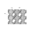
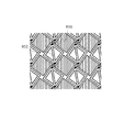
検出電極における寄生容量を好適に削減するため、本発明では、検出電極の新規な構造を考案した。図4に本発明の構成の一例を示す。図4(A)は、図2(B)に示したものと同様、タッチセンサ電極の平面構成を示している。図4(B)は、図4(A)のZ−Z’間の断面構造を示している。 In order to suitably reduce the parasitic capacitance in the detection electrode, a novel structure of the detection electrode has been devised in the present invention. FIG. 4 shows an example of the configuration of the present invention. FIG. 4A shows a planar configuration of the touch sensor electrode, similar to that shown in FIG. FIG. 4B illustrates a cross-sectional structure taken along the line Z-Z ′ in FIG.
図4(B)において、基板101、TFTアレイ301、発光素子層302、封止層303は図3にて示したものと同様であり、タッチセンサ304の構造をより詳細に示している。検出電極401、402と、駆動配線404とは、同層に配置されており、検出電極401と402との間は、駆動配線404を乗り越えるブリッジ配線403によって接続されている。
4B, the
図4(A)に示すように、検出電極401、402はその形状を環状形状としている。具体的には、電極の外周形状はそのままに、内部領域を中空とした環状形状としている。従来のように内部領域が中実となった検出電極と比較して電極面積が縮小しているため、下層の発光素子層302等との間の寄生容量Cpを減少させることができる。
As shown in FIG. 4A, the
ここで、検出電極401、402の形状について述べる。寄生容量低減を目的として検出電極の面積を縮小する際、単に形状を縮小してもその効果は同様である。しかし、タッチ検出動作において重要となる駆動電極と検出電極とのカップリング容量Cxyは、両者が最も近接する領域、すなわち電極の周縁部での寄与が大きい。従って、検出電極の内部領域を中空として面積を縮小することにより、カップリング容量Cxyを減らすことなく、好適に寄生容量Cpを減らすことができる。
Here, the shape of the
検出電極を環状形状とした場合と、従来形状とした場合との、寄生容量Cpとカップリング容量Cxyの変化を図5に示す。図4(A)において、検出電極を環状形状とした場合の環の幅をa、検出電極の全幅をbとし、両者の比a/bとしたものを横軸に取っている。中空部分が無い従来形状の場合、a/b=1/2で最大となる。また、検出電極を環状形状とした場合と従来形状とした場合のカップリング容量の比(Chollow/Csolid)を縦軸に取っている。両者のカップリング容量が等しい場合、(Chollow/Csolid)=1で最大となる。 FIG. 5 shows changes in the parasitic capacitance Cp and the coupling capacitance Cxy when the detection electrode has an annular shape and when the detection electrode has a conventional shape. In FIG. 4A, when the detection electrode has an annular shape, the width of the ring is a, the entire width of the detection electrode is b, and the ratio a / b of both is taken on the horizontal axis. In the case of a conventional shape having no hollow portion, a / b = 1/2 is the maximum. In addition, the vertical axis represents the ratio (Chollow / Csolid) of the coupling capacity when the detection electrode has an annular shape and the conventional shape. When both coupling capacities are equal, (Chollow / Csolid) = 1 is the maximum.
検出電極の全幅bを一定として環の幅aを大きくしていくと、検出電極の面積が大きくなるに従って寄生容量Cpは増大する。一方で、カップリング容量の比は、環の幅aがある程度の値になったところで、ほぼ従来形状に対して1:1に到達する。つまり、このときの環の幅a1を最小値として、これ以上の値を有するように検出電極の形状を決定することで、カップリング容量Cxyを維持したまま寄生容量Cpを好適に減少させることができ、検出信号の振幅を大きくとることができる。 If the entire width b of the detection electrode is kept constant and the ring width a is increased, the parasitic capacitance Cp increases as the area of the detection electrode increases. On the other hand, the ratio of the coupling capacity almost reaches 1: 1 with respect to the conventional shape when the ring width a reaches a certain value. That is, the parasitic capacitance Cp can be suitably reduced while maintaining the coupling capacitance Cxy by determining the shape of the detection electrode so that the ring width a1 at this time is the minimum value and has a value larger than this. The amplitude of the detection signal can be increased.
一例として、図4(A)に示したタッチセンサ上に、比誘電率5.7、板厚700μmのカバーガラスを設けた系において、検出電極の全幅b=3mmとした場合の計算結果によると、a1=800μmが得られた。つまり、3mm□の検出電極内部に1.4mm□の穴を設けた環状構造とすることで、駆動電極とのカップリング容量は従来と同等としつつ、寄生容量を好適に低減する構成を実現できる。 As an example, in the system in which a cover glass having a relative dielectric constant of 5.7 and a plate thickness of 700 μm is provided on the touch sensor shown in FIG. A1 = 800 μm was obtained. In other words, by adopting an annular structure in which a 1.4 mm □ hole is provided inside a 3 mm □ detection electrode, it is possible to realize a configuration in which parasitic capacitance is suitably reduced while the coupling capacitance with the drive electrode is equal to that of the conventional one. .
なお、本構造では、寄生容量の低減に加え、発光素子層302を駆動するTFTアレイ301からのノイズを軽減する効果も併せ持つ。TFTアレイ301の駆動信号によるノイズは、発光素子層302を介して検出電極401、402に伝わるが、電極面積を小さくすることで、容量カップリングを低減でき、ノイズを軽減させることができる。
Note that this structure has the effect of reducing noise from the
ここで、図4に示したタッチセンサの形成方法について説明する。ここでは、TFTアレイ301、発光素子層302、及び封止層303の形成工程については省略する。
Here, a method for forming the touch sensor shown in FIG. 4 will be described. Here, the steps for forming the
封止膜表面に、検出電極401、402、及び駆動電極404を形成する。ここではITO、IZO等の透明導電材料をスパッタリングにて成膜後、フォトリソグラフィプロセスにより形成する。発光素子層302上に形成した封止層303が十分な被覆性と密着性を有しているため、発光素子層302の形成後であっても前述のようなプロセスの適用が可能である。先の透明導電材料に代えて、銀ナノワイヤを含む材料を印刷形成して検出電極401、402、及び駆動電極404を形成してもよい。次に絶縁膜を形成後、検出電極401、402に到達するコンタクトホールを形成し、ブリッジ電極403を形成する。ブリッジ電極403は面積が小さく視認されにくいので、低抵抗化を優先してアルミニウム、銀、銅等の金属を成膜後、フォトリソグラフィプロセスにより形成する。その後、必要であればさらに絶縁膜形成もしくはフィルム貼付等により、電極パターンの保護を行ってもよい。以上の工程により、表示領域上にタッチセンサを形成することができる。
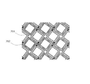
本発明の他の例として、図6、図7のような構造としても良い。図6は、環状とした検出電極601の一部に切り欠きを設け、当該切り欠きを介して、駆動電極602が突出部610を有し、この突出部610が環の内側に入り込む形状としている。検出電極601の寄生容量を小さくすると共に、突出部610と検出電極601との間でさらにカップリング容量を増加することができる。図7は、検出電極701に加えて、駆動電極702も環状形状とした例を示している。駆動電極は低インピーダンスで駆動されるため、検出電極ほど外部の電界変動の影響を受けないが、透明導電材料にて形成されている場合は、金属と比べて抵抗が高いことから、面内の中心領域、すなわち駆動電極を駆動する回路から遠い領域では、TFTアレイ等からのノイズの影響を受けやすくなる。駆動電極702を環状形状とすることで、ノイズの影響を軽減することができ、面内全域において安定したタッチ検出が可能となる。
As another example of the present invention, a structure as shown in FIGS. 6 and 7 may be used. In FIG. 6, a notch is formed in a part of the
図8は、前述とはさらに異なる構成例を示している。環状とした検出電極801の対角線上にリブ802を設けたものであり、環状の検出電極に比べて時定数を低減することができる。
FIG. 8 shows a configuration example further different from the above. The
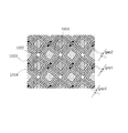
前述のように、検出電極又は駆動電極を環状形状とすることにより、電気的には顕著な機能向上が期待できる反面、駆動電極が設けられた領域と設けられていない領域とに分かれることで、両者の間に屈折率の差が生じ、検出電極の環状形状が視認されてしまう場合がある。そこで、図9に示すように、環状形状を有する検出電極901の内側に、検出電極901と同層の材料で内部電極902を形成する。内部電極902を設けることで、面内の屈折率を均一にすることができるため、検出電極の視認性を下げることができる。
As described above, by making the detection electrode or the drive electrode into an annular shape, it is possible to expect a significant improvement in function electrically, but on the other hand, it is divided into a region where the drive electrode is provided and a region where the drive electrode is not provided. There may be a difference in refractive index between the two, and the annular shape of the detection electrode may be visually recognized. Therefore, as shown in FIG. 9, an
内部電極902は、検出電極901、及び駆動電極903のいずれとも絶縁されており、浮遊状態となっているが、内部電極902と検出電極901との距離が短いと、検出電極901と発光素子層302との間に、内部電極902を介して寄生容量が生ずる場合がある。
The
環状形状の検出電極901と、駆動電極903との間の距離をgap1、環状形状の検出電極901と、内部電極902との間の距離をgap2とすると、gap1は検出電極と駆動電極との間のカップリング容量に影響するため、gap1は狭いことが望ましい。また、環状形状の検出電極の視認性を考えると、gap2は狭いことが望ましい。しかし、gap2を狭くすると、環状形状の検出電極901と発光素子層302との間で、内部電極902を介して寄生容量が増加してしまう。従って、gap2はgap1よりも広くすることが好ましい。
If the distance between the
図10は、図8と同様に、検出電極に設けた環状形状および内部電極を、駆動電極側にも適用した例を示している。環状の検出電極1001の内側に内部電極1002を形成し、環状の駆動電極1003の内側に内部電極1004を形成している。
FIG. 10 shows an example in which the annular shape and the internal electrode provided on the detection electrode are applied to the drive electrode side as in FIG. An
環状の駆動電極1002と、内部電極1004との間の距離をgap3とする。駆動電極1002は検出電極1001に比べて、TFTアレイ301や発光素子層302からのノイズの影響は小さいので、gap3はgap2よりも小さくしても構わない。これらの関係は、例えばgap1<gap3≦gap2等とすればよい。
The distance between the
本発明の思想の範疇において、当業者であれば、各種の変更例及び修正例に想到し得るものであり、それら変更例及び修正例についても本発明の範囲に属するものと了解される。例えば、前述の各実施形態に対して、当業者が適宜、構成要素の追加、削除若しくは設計変更を行ったもの、又は、工程の追加、省略若しくは条件変更を行ったものも、本発明の要旨を備えている限り、本発明の範囲に含まれる。 In the scope of the idea of the present invention, those skilled in the art can conceive various changes and modifications, and it is understood that these changes and modifications also belong to the scope of the present invention. For example, those in which the person skilled in the art has appropriately added, deleted, or changed the design of the above-described embodiments, or those in which processes have been added, omitted, or changed conditions are also the subject matter of the present invention As long as it is provided, it is included in the scope of the present invention.
100:表示装置、101:基板、102:表示領域、103,104:走査線駆動回路、105:ドライバIC、106:表示用FPC、107:タッチ用FPC、108:対向基板、109:画素、109a:副画素、110:走査線、120:映像信号線、201,404,602,702,903,1003:駆動電極、202,401,402,601,701,801,901,1001:検出電極、203,403:ブリッジ配線、301:TFTアレイ、302:発光素子層、303:封止層、304:タッチセンサ、305:円偏光板、306:カバーガラス、610:突出部、802:リブ、902,1002,1004:リブ
100: Display device, 101: Substrate, 102: Display area, 103, 104: Scan line driving circuit, 105: Driver IC, 106: Display FPC, 107: Touch FPC, 108: Counter substrate, 109: Pixel, 109a : Sub-pixel, 110: scanning line, 120: video signal line, 201, 404, 602, 702, 903, 1003: drive electrode, 202, 401, 402, 601, 701, 801, 901, 1001: detection electrode, 203 403: Bridge wiring 301: TFT array 302: Light emitting
Claims (7)
前記タッチセンサは、複数の第1電極と、複数の第2電極と、を有し、
前記複数の第1電極は、環状形状の電極が連なった形状を有することを特徴とする、表示装置。 A display device having a display area in which a plurality of pixels each having a light emitting element and a transistor are arranged in a matrix, and a touch sensor provided on the display area,
The touch sensor has a plurality of first electrodes and a plurality of second electrodes,
The display device according to claim 1, wherein the plurality of first electrodes have a shape in which annular electrodes are connected.
前記第2電極は、突出部を有し、
前記突出部は、前記切り欠き部を通じて、前記環状形状の電極の内側に入り込むことを特徴とする、請求項1記載の表示装置。 The annular electrode has a notch,
The second electrode has a protrusion,
The display device according to claim 1, wherein the protruding portion enters the inside of the annular electrode through the cutout portion.
前記複数の第1電極と、前記複数の第2電極とは、前記封止膜上に形成されていることを特徴とする、請求項1記載の表示装置。
A sealing layer on the display region;
The display device according to claim 1, wherein the plurality of first electrodes and the plurality of second electrodes are formed on the sealing film.
Priority Applications (5)
| Application Number | Priority Date | Filing Date | Title |
|---|---|---|---|
| JP2016043910A JP2017162032A (en) | 2016-03-07 | 2016-03-07 | Display device |
| TW106105792A TWI652616B (en) | 2016-03-07 | 2017-02-21 | Display device |
| US15/446,461 US20170255310A1 (en) | 2016-03-07 | 2017-03-01 | Display device |
| KR1020170027053A KR20170104384A (en) | 2016-03-07 | 2017-03-02 | Display device |
| CN201710128397.6A CN107168592A (en) | 2016-03-07 | 2017-03-06 | Display device |
Applications Claiming Priority (1)
| Application Number | Priority Date | Filing Date | Title |
|---|---|---|---|
| JP2016043910A JP2017162032A (en) | 2016-03-07 | 2016-03-07 | Display device |
Publications (1)
| Publication Number | Publication Date |
|---|---|
| JP2017162032A true JP2017162032A (en) | 2017-09-14 |
Family
ID=59722694
Family Applications (1)
| Application Number | Title | Priority Date | Filing Date |
|---|---|---|---|
| JP2016043910A Pending JP2017162032A (en) | 2016-03-07 | 2016-03-07 | Display device |
Country Status (5)
| Country | Link |
|---|---|
| US (1) | US20170255310A1 (en) |
| JP (1) | JP2017162032A (en) |
| KR (1) | KR20170104384A (en) |
| CN (1) | CN107168592A (en) |
| TW (1) | TWI652616B (en) |
Families Citing this family (5)
| Publication number | Priority date | Publication date | Assignee | Title |
|---|---|---|---|---|
| CN105353931B (en) * | 2015-11-24 | 2019-03-15 | 京东方科技集团股份有限公司 | Touch screen and preparation method thereof, display device |
| CN107994057B (en) * | 2017-11-20 | 2021-09-28 | 武汉华星光电半导体显示技术有限公司 | Manufacturing method of touch sensing layer, display screen and display |
| CN111158533B (en) * | 2019-11-28 | 2024-04-23 | 京东方科技集团股份有限公司 | Detection substrate and display device |
| JP2021148616A (en) * | 2020-03-19 | 2021-09-27 | 株式会社ジャパンディスプレイ | Display device and watch |
| CN115145424A (en) * | 2022-06-28 | 2022-10-04 | 上海天马微电子有限公司 | Sensing unit and sensing device |
Family Cites Families (12)
| Publication number | Priority date | Publication date | Assignee | Title |
|---|---|---|---|---|
| US6879319B2 (en) * | 2002-10-25 | 2005-04-12 | Eastman Kodak Company | Integrated OLED display and touch screen |
| WO2009139205A1 (en) * | 2008-05-13 | 2009-11-19 | シャープ株式会社 | Display device and television reception device |
| KR101634791B1 (en) * | 2008-11-28 | 2016-06-30 | 삼성디스플레이 주식회사 | Touch sensible organic light emitting diode display |
| JP5458443B2 (en) * | 2010-09-14 | 2014-04-02 | 株式会社ジャパンディスプレイ | Display device with touch detection function and electronic device |
| CN102985835B (en) * | 2011-07-15 | 2018-04-13 | 赛普拉斯半导体公司 | Capacitance sensing circuit, method and system with ground connection insertion electrode |
| KR101853025B1 (en) * | 2011-07-27 | 2018-04-27 | 엘지디스플레이 주식회사 | Touch screen panel |
| JP3179159U (en) * | 2012-08-06 | 2012-10-18 | 介面光電股▲ふん▼有限公司 | Capacitive touch detector |
| KR102251870B1 (en) * | 2014-05-12 | 2021-05-14 | 엘지이노텍 주식회사 | Touch window |
| WO2015174688A1 (en) * | 2014-05-12 | 2015-11-19 | Lg Innotek Co., Ltd. | Touch window |
| KR101719397B1 (en) * | 2014-08-14 | 2017-03-24 | 엘지디스플레이 주식회사 | Touch sensor integrated type liquid crystal display device |
| CN104461158A (en) * | 2014-12-26 | 2015-03-25 | 合肥鑫晟光电科技有限公司 | Touch panel and display device |
| KR102362189B1 (en) * | 2015-04-16 | 2022-02-11 | 삼성디스플레이 주식회사 | Organic light emitting diode display |
-
2016
- 2016-03-07 JP JP2016043910A patent/JP2017162032A/en active Pending
-
2017
- 2017-02-21 TW TW106105792A patent/TWI652616B/en active
- 2017-03-01 US US15/446,461 patent/US20170255310A1/en not_active Abandoned
- 2017-03-02 KR KR1020170027053A patent/KR20170104384A/en active Search and Examination
- 2017-03-06 CN CN201710128397.6A patent/CN107168592A/en active Pending
Also Published As
| Publication number | Publication date |
|---|---|
| CN107168592A (en) | 2017-09-15 |
| US20170255310A1 (en) | 2017-09-07 |
| KR20170104384A (en) | 2017-09-15 |
| TW201732536A (en) | 2017-09-16 |
| TWI652616B (en) | 2019-03-01 |
Similar Documents
| Publication | Publication Date | Title |
|---|---|---|
| US10168565B2 (en) | In-cell touch display device | |
| TWI652616B (en) | Display device | |
| US11847274B2 (en) | Touch display device and touch panel | |
| JP5103254B2 (en) | Capacitive touch panel and screen input type display device including the same | |
| US10031626B2 (en) | Display device with integrated touch screen | |
| JP6253923B2 (en) | Organic electroluminescence device with built-in touch sensor | |
| US10732744B2 (en) | Display device including touch sensor | |
| US20180059869A1 (en) | Touch sensor and touch screen | |
| TWI460639B (en) | System for display images | |
| US20170269762A1 (en) | Array substrate, related display panels, and related display apparatus | |
| US10372278B2 (en) | Display device and detection device | |
| JP2018055236A (en) | Touch sensor and display device with touch sensor | |
| TW201738714A (en) | Dual-mode capacitive touch display panel | |
| US11088220B2 (en) | Display device including touch sensor and method of manufacturing the same | |
| US10592028B2 (en) | Touch sensor feedlines for display | |
| KR102649110B1 (en) | Array Substrate For Touch Display Device And Method Of Fabricating The Same | |
| JP6663753B2 (en) | Display device | |
| US10949039B2 (en) | Display device | |
| KR20190048985A (en) | Display device with touch sensor and manufacturing method for the same | |
| CN101819494A (en) | Image display system | |
| JP6742822B2 (en) | Display device | |
| CN112181215B (en) | Touch display panel, touch detection method thereof and electronic equipment | |
| JP2018206350A (en) | Touch display device | |
| CN110291607B (en) | Display device | |
| JP6517910B2 (en) | Touch sensor built-in organic EL device |