JP2017153254A - Parts for semiconductor manufacturing apparatus - Google Patents
Parts for semiconductor manufacturing apparatus Download PDFInfo
- Publication number
- JP2017153254A JP2017153254A JP2016033729A JP2016033729A JP2017153254A JP 2017153254 A JP2017153254 A JP 2017153254A JP 2016033729 A JP2016033729 A JP 2016033729A JP 2016033729 A JP2016033729 A JP 2016033729A JP 2017153254 A JP2017153254 A JP 2017153254A
- Authority
- JP
- Japan
- Prior art keywords
- lead terminal
- semiconductor manufacturing
- manufacturing apparatus
- electrode layer
- substrate
- Prior art date
- Legal status (The legal status is an assumption and is not a legal conclusion. Google has not performed a legal analysis and makes no representation as to the accuracy of the status listed.)
- Granted
Links
Images


Abstract
Description
本発明は、半導体製造装置用部品に関するものである。 The present invention relates to a component for a semiconductor manufacturing apparatus.
半導体製造装置用部品として、例えば、特許文献1に記載の給電端子の接合構造が知られている。特許文献1に記載の給電端子の接合構造は、表面に凹部を有するセラミック部材と、セラミック部材の内部に設けられて凹部の底面に一部が露出した内部電極と、凹部に挿入されるとともに内部電極にろう付けによって接合された給電端子とを備えている。
As a component for a semiconductor manufacturing apparatus, for example, a joint structure of a power feeding terminal described in
しかしながら、特許文献1に開示された給電端子の接合構造においては、ヒートサイクル下において、給電端子とセラミック部材との間に熱応力が生じるおそれがあった。その結果、セラミック部材にクラックが生じるおそれがあった。
However, in the joint structure of the power supply terminal disclosed in
本発明の一態様の半導体製造装置用部品は、セラミックスからなる基体と、該基体の内部に設けられた電極層と、前記基体の表面に導電性の接合材によって接合されるとともに前記電極層に電気的に接続されたリード端子とを備えており、前記基体が、前記表面のうち前記リード端子が接合された領域に、同心円状の複数の溝部を有することを特徴とする。 A component for a semiconductor manufacturing apparatus according to an aspect of the present invention includes a base made of ceramics, an electrode layer provided inside the base, and a surface of the base that is bonded to the surface of the base by a conductive bonding material. And the base has a plurality of concentric grooves in a region of the surface where the lead terminals are joined.
本発明の一態様の半導体製造装置用部品においては、基体が、リード端子が接合された領域に、同心円状の複数の溝部を有することによって、熱応力を周方向に分散させることができる。これにより、特定の部位に熱応力が集中することを低減できる。その結果、基体にクラックが生じるおそれを低減できる。 In the semiconductor manufacturing apparatus component of one embodiment of the present invention, the base has a plurality of concentric grooves in the region where the lead terminals are joined, so that thermal stress can be dispersed in the circumferential direction. Thereby, it can reduce that a thermal stress concentrates on a specific site | part. As a result, the risk of cracks occurring in the substrate can be reduced.
本発明の一実施形態の半導体製造装置用部品10について詳細に説明する。
The semiconductor
図1に示すように、半導体製造装置用部品10は、基体1と、基体1の内部に設けられ
た電極層2とを備えている。半導体製造装置用部品10は、例えば、静電チャックとして用いられる。この場合には、電極層2は、例えば、静電吸着用電極として用いられる。
As shown in FIG. 1, the semiconductor
半導体製造装置用部品10が静電チャックとして用いられる場合には、基体1は試料を保持するための部材である。基体1は、積層体から成る。基体1は、例えば、円板状の部材である。基体1は、例えば、窒化アルミニウム等のセラミック材料から成る。基体1は、例えば、複数のグリーンシートを積層して、これを窒素雰囲気中で焼成することによって得ることができる。基体1の内部には電極層2が設けられている。このような構成にするためには、上述した焼成前の複数のグリーンシートのうち所望のグリーンシートにスクリーン印刷法等を用いて、焼成後に電極層2と成るパターンを印刷しておけばよい。基体1の寸法は、例えば、主面の直径を30〜500mm程度に、厚みを5〜25mm程度に設定できる。
When the semiconductor
半導体製造装置用部品10が静電チャックとして用いられる場合には、電極層2は静電吸着力によって試料を保持するための部材である。電極層2は、例えば、基体1の主面と対向するように円状に設けられている。電極層2は、例えば、タングステン等の金属材料から成る。
When the semiconductor
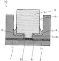
図2に示すように、本実施形態の半導体製造装置用部品10においては、基体1の表面に電極層2と外部の電源(図示せず)との電気的な接続を行なうための凹部5が設けられている。凹部5の内表面には電極層2が露出している。より具体的には、凹部5の底面に電極層2が露出している。基体1の表面にはリード端子3が設けられている。なお、図2は部分断面図であるため、基体1、電極層2およびリード端子3等は接合部分およびその周辺のみを局所的に示している。リード端子3は、電極層2と外部の電源とを電気的に接続するための部材である。
As shown in FIG. 2, in the semiconductor
リード端子3は、電極層2に導電性の接合材4によって接合(固定)されているとともに、電極層2に電気的に接続されている。リード端子3は、基体1の表面から垂直方向に伸びるように設けられている。リード端子3は、例えば、断面の形状が円状の棒状または針金状の部材である。リード端子3の材料としては、例えば、金、銅または黄銅等の銅系合金を用いることができる。また、その他のリード端子3の材料としては、例えば、ニッケル、Fe−Ni−Co合金またはFe−Ni−Cr合金等を用いることができる。
The
本実施形態においては、リード端子3の径は凹部5の径よりも大きい。リード端子3の端面は凹部5の開口部を覆っている。接合材4は凹部5に充填されるとともに、基体1の表面のうち凹部5の周囲にまで広がっている。接合材4は、基体1の表面とリード端子3の端面との間を濡れ広がっている。接合材4としては、例えば、銀銅ろうまたは半田等を用いることができる。
In the present embodiment, the diameter of the
ここで、本実施形態の半導体製造装置用部品10においては、基体1が、表面のうちリード端子3が接合された領域に、同心円状の複数の溝部6を有している。なお、ここでいう「接合された領域」とは、基体1の表面のうち電極層2とリード端子3とを固定する接合材4が濡れ広がっている領域を意味している。
Here, in the semiconductor
このように、リード端子3が接合された領域に、同心円状の複数の溝部6を有することによって、熱応力を周方向に分散させることができる。これにより、特定の部位に熱応力が集中することを低減できる。その結果、基体1にクラックが生じるおそれを低減できる。溝部6の寸法は、例えば、溝部6の幅を0.5mm〜10mm、溝部6同士の間隔を0.05mm〜1mm好ましくは0.1mm〜0.5mm、溝部6の深さを0.01mm〜0.5mm好ましくは0.02mm〜0.2mmに設定できる。
As described above, by having the plurality of
溝部6の断面形状は、例えば、U字状またはV字状等に設定できる。溝部6の形状がU字状である場合には、溝部6の底面の形状が緩やかになるので溝部6においてクラックが生じるおそれを低減できる。
The cross-sectional shape of the
溝部6は、例えば、マニシング加工によって形成することができる。具体的には、ダイヤモンド等からなる加工ツールを用いて、同心円状の溝部6を形成することができる。
The
複数の溝部6のうち、中心側に位置する溝部6よりも外周側に位置する溝部6のほうが幅が大きくなっていてもよい。これにより、ヒートサイクル下において熱応力が生じたとしても、この熱応力をリード端子3の端面の中心側に集中させることができる。リード端子3の中心側は外周側と比較してクラック等が入りにくい。これは、リード端子3の外周側には、リード端子3の端面と外周面とによって形成される角部があることから熱応力が生じたときに、クラック等が生じやすい状態にある。これに対してリード端子3の端面の中心側は角部が存在しないことからクラックの起点となる部分が存在しにくい点が理由として挙げられる。これらの理由により、リード端子3の耐久性を向上させることができる。
Of the plurality of
ここでいう、中心側および外周側とは、例えば、以下のように定義できる。具体的には、リード端子3の端面が円形状の場合には、リード端子3の端面の中心と同じ中心を有しており径が半分の大きさの仮想円を考えたときに、この仮想円の内側を中心側として外側を外周側と見なすことができる。
Here, the center side and the outer peripheral side can be defined as follows, for example. Specifically, when the end face of the
また、複数の溝部6のうち、リード端子3の外周の直下に位置する部分の深さが、リード端子3の直下に位置する他の部分の深さよりも、大きくなっていてもよい。この場合には、リード端子3の外周面に濡れ広がった接合材4が形成するメニスカスの曲率を大きくできる。そのため、リード端子3が傾く方向の力がリード端子3に加わった際の接合の耐久性を向上させることができる。
Moreover, the depth of the part located directly under the outer periphery of the
また、複数の溝部6のうち、リード端子3の外周の直下に位置する部分の幅が、リード端子3の直下に位置する他の部分の幅よりも大きくてもよい。この場合には、リード端子3の外周面に濡れ広がった接合材4が形成するメニスカスの高さ(深さ)を大きくできる。そのため、リード端子3が傾く方向の力がリード端子3に加わった際の接合の耐久性を向上させることができる。
In addition, among the plurality of
また、図3に示すように、リード端子3が内部に空洞32を有していてもよい。空洞32は、リード端子3のうち電極層2に接合される端面に開口している。言い換えると、リード端子3が中空状であってもよい。また、リード端子3が筒状であってもよい。リード端子3が空洞32を有している場合であっても、上述した複数の溝部6を跨って覆うようにリード端子3の端面が位置していれば上述した効果を得ることができる。リード端子3が空洞32を有している場合には、接合材4の一部がリード端子3の内周側に入り込んでいてもよい。これにより、リード端子3をより強固に基体1に固定することができる。
Moreover, as shown in FIG. 3, the
また、図4に示すように、基体1が表面にリード端子3を挿入するための凹部5を有していてもよい。このとき、リード端子3の少なくとも一部が凹部5に挿入されており、凹部5の底面に接合されていてもよい。図4に示す半導体製造装置用部品10においては、底面に電極層2が露出している。この電極層2および接合材4を介して、リード端子3が凹部5の底面に接合されている。
Moreover, as shown in FIG. 4, the base |
基体1が、表面にリード端子3を挿入するための凹部5を有するとともに、リード端子
3が凹部5の底面に接合されていることによって、リード端子3の位置決めを行ないやすくできる。これにより、リード端子3と電極層2との接続の信頼性を向上できる。
The
リード端子3は、凹部5に挿入される先端部分が残部と比較して径が小さくなっている。言い換えると、リード端子3は先端に縮径部31を有している。リード端子3の縮径部31は凹部5に挿入されている。接合材4は、凹部5の内部において縮径部31と電極層2とを固定するとともに、基体1の表面のうち凹部5の周囲にも濡れ広がっている。接合材4のうち凹部5の周囲に濡れ広がった部分は、リード端子3の残部を固定している。さらに言い換えると、リード端子3は先端に凸部31を有しており、この凸部31が基体1の凹部5に挿入されている。接合材4はリード端子3の端面のうち凸部31を含む全体に濡れ広がっている。これにより、リード端子3を強固に固定できる。また、図5に示すように、リード端子3を凹部5に挿入する場合も、リード端子3が空洞32を有していてもよい。
The
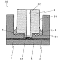
また、図6、7に示すように、凹部5が二重に形成されていてもよい。具体的には、リード端子3の端部の全体が挿入される第1凹部51と、第1凹部51の底面に形成されており、リード端子3の端面に形成された凸部31が挿入される第2凹部52とを有していてもよい。これにより、第1凹部51とリード端子3の外周面との間、および、第2凹部52と凸部31との間に接合材4を濡れ広がらせることができるので、接合強度を向上できる。
Moreover, as shown to FIG. 6, 7, the recessed
また、図6、7に示すように、第1凹部51の底面に複数の溝部6が形成されるとともに、第2凹部52の底面にも複数の溝部6が形成されていてもよい。第2凹部52の底面に複数の溝部6が形成されているとともに、この上に設けられた電極層2もこの複数の溝部6の形状を反映して表面に凹凸が出来ていてもよい。これにより、電極層2とリード端子3とを接合材4で接合したときに、熱応力を周方向に分散させることができる。これにより、特定の部位に熱応力が集中することを低減できる。なお、図4に示す半導体製造装置用部品10においても、凹部5の底面に同様の溝部6が形成されていてもよい。そして、この溝部6の形状を反映して電極層2の表面に凹凸が出来ていてもよい。
As shown in FIGS. 6 and 7, a plurality of
また、図8に示すように、基体1にリード端子3が挿入される凹部5が設けられるとともに、凹部5の底面に複数の溝部6が形成されていてもよい。この場合にも、複数の溝部6の上に設けられた電極層2もこの複数の溝部6の形状を反映して表面に凹凸が出来ていてもよい。これにより、電極層2とリード端子3とを接合材4で接合したときに、熱応力を周方向に分散させることができる。これにより、特定の部位に熱応力が集中することを低減できる。
Further, as shown in FIG. 8, a
また、リード端子3が、接合材4よりも硬度が大きくてもよい。これにより、熱応力が生じたときにリード端子3よりも接合材4に変形を生じさせることができる。これにより、リード端子3の位置の精度を高めることができる。リード端子3が接合材4よりも硬度が大きい場合としては、以下の例が挙げられる。具体的には、接合材4として、例えば、Sn−Ag−Cu系半田、Sn−Zn−Al系またはSn−Zn−Bi系等のSn−Zn系半田を用いる場合には、リード端子3として、例えば、銅、黄銅またはFe−Ni−Co合金等の接合材4よりも高い硬度を有する材料を用いることができる。硬度の比較は以下の方法で行なうことができる。具体的にはJIS Z 2244に基づき、ビッカース硬度Hvを測定することで硬度の比較ができる。
Further, the
1:基体
2:電極層
3:リード端子
31:凸部、縮径部
32:空洞
4:接合材
5:凹部
51:第1凹部
52:第2凹部
6:溝部
10:半導体製造装置用部品
1: Base body 2: Electrode layer 3: Lead terminal 31: Convex part, reduced diameter part 32: Cavity 4: Bonding material 5: Concave material 51: First concavity 52: Second concavity 6: Groove part 10: Parts for semiconductor manufacturing equipment
Claims (7)
前記基体が、前記表面のうち前記リード端子が接合された領域に、同心円状の複数の溝部を有することを特徴とする半導体製造装置用部品。 A substrate made of ceramic, an electrode layer provided inside the substrate, and a lead terminal bonded to the surface of the substrate by a conductive bonding material and electrically connected to the electrode layer. ,
A component for a semiconductor manufacturing apparatus, wherein the base has a plurality of concentric grooves in a region of the surface where the lead terminals are joined.
前記リード端子が前記凹部の底面に接合されていることを特徴とする請求項1に記載の半導体製造装置用部品。 The base has a recess for inserting the lead terminal on the surface;
The component for a semiconductor manufacturing apparatus according to claim 1, wherein the lead terminal is bonded to a bottom surface of the concave portion.
Priority Applications (1)
| Application Number | Priority Date | Filing Date | Title |
|---|---|---|---|
| JP2016033729A JP6591911B2 (en) | 2016-02-25 | 2016-02-25 | Parts for semiconductor manufacturing equipment |
Applications Claiming Priority (1)
| Application Number | Priority Date | Filing Date | Title |
|---|---|---|---|
| JP2016033729A JP6591911B2 (en) | 2016-02-25 | 2016-02-25 | Parts for semiconductor manufacturing equipment |
Publications (2)
| Publication Number | Publication Date |
|---|---|
| JP2017153254A true JP2017153254A (en) | 2017-08-31 |
| JP6591911B2 JP6591911B2 (en) | 2019-10-16 |
Family
ID=59739257
Family Applications (1)
| Application Number | Title | Priority Date | Filing Date |
|---|---|---|---|
| JP2016033729A Active JP6591911B2 (en) | 2016-02-25 | 2016-02-25 | Parts for semiconductor manufacturing equipment |
Country Status (1)
| Country | Link |
|---|---|
| JP (1) | JP6591911B2 (en) |
Cited By (3)
| Publication number | Priority date | Publication date | Assignee | Title |
|---|---|---|---|---|
| WO2020004564A1 (en) * | 2018-06-28 | 2020-01-02 | 京セラ株式会社 | Method for producing member for semiconductor production apparatuses, and member for semiconductor production apparatuses |
| WO2020110850A1 (en) * | 2018-11-30 | 2020-06-04 | 京セラ株式会社 | Ceramic structure and method of manufacturing ceramic structure |
| KR20210047957A (en) * | 2018-09-20 | 2021-04-30 | 램 리써치 코포레이션 | Long life, high power terminals for substrate support with embedded heating elements |
Citations (7)
| Publication number | Priority date | Publication date | Assignee | Title |
|---|---|---|---|---|
| JPH11220011A (en) * | 1998-01-30 | 1999-08-10 | Kyocera Corp | Terminal structure |
| JP2007123601A (en) * | 2005-10-28 | 2007-05-17 | Ngk Insulators Ltd | Ceramic substrate and bonding structure of electrical connector for power supplies |
| WO2008035395A1 (en) * | 2006-09-19 | 2008-03-27 | Creative Technology Corporation | Feeding structure of electrostatic chuck, method for producing the same, and method for regenerating feeding structure of electrostatic chuck |
| JP2008198975A (en) * | 2007-01-17 | 2008-08-28 | Tokyo Electron Ltd | Mounting table structure and processing apparatus |
| JP2010034514A (en) * | 2008-07-01 | 2010-02-12 | Ngk Insulators Ltd | Junction structure, method of manufacturing the same, and electrostatic chuck |
| WO2015146563A1 (en) * | 2014-03-27 | 2015-10-01 | 日本碍子株式会社 | Joined structure between ceramic plate and metallic cylindrical member |
| JP2017212406A (en) * | 2016-05-27 | 2017-11-30 | 京セラ株式会社 | Member for electrostatic attraction |
-
2016
- 2016-02-25 JP JP2016033729A patent/JP6591911B2/en active Active
Patent Citations (7)
| Publication number | Priority date | Publication date | Assignee | Title |
|---|---|---|---|---|
| JPH11220011A (en) * | 1998-01-30 | 1999-08-10 | Kyocera Corp | Terminal structure |
| JP2007123601A (en) * | 2005-10-28 | 2007-05-17 | Ngk Insulators Ltd | Ceramic substrate and bonding structure of electrical connector for power supplies |
| WO2008035395A1 (en) * | 2006-09-19 | 2008-03-27 | Creative Technology Corporation | Feeding structure of electrostatic chuck, method for producing the same, and method for regenerating feeding structure of electrostatic chuck |
| JP2008198975A (en) * | 2007-01-17 | 2008-08-28 | Tokyo Electron Ltd | Mounting table structure and processing apparatus |
| JP2010034514A (en) * | 2008-07-01 | 2010-02-12 | Ngk Insulators Ltd | Junction structure, method of manufacturing the same, and electrostatic chuck |
| WO2015146563A1 (en) * | 2014-03-27 | 2015-10-01 | 日本碍子株式会社 | Joined structure between ceramic plate and metallic cylindrical member |
| JP2017212406A (en) * | 2016-05-27 | 2017-11-30 | 京セラ株式会社 | Member for electrostatic attraction |
Cited By (9)
| Publication number | Priority date | Publication date | Assignee | Title |
|---|---|---|---|---|
| WO2020004564A1 (en) * | 2018-06-28 | 2020-01-02 | 京セラ株式会社 | Method for producing member for semiconductor production apparatuses, and member for semiconductor production apparatuses |
| JPWO2020004564A1 (en) * | 2018-06-28 | 2021-07-15 | 京セラ株式会社 | Manufacturing method of semiconductor manufacturing equipment members and semiconductor manufacturing equipment members |
| KR20210047957A (en) * | 2018-09-20 | 2021-04-30 | 램 리써치 코포레이션 | Long life, high power terminals for substrate support with embedded heating elements |
| JP2022500865A (en) * | 2018-09-20 | 2022-01-04 | ラム リサーチ コーポレーションLam Research Corporation | Long-life high-output terminals for substrate supports with embedded heating elements |
| JP7269327B2 (en) | 2018-09-20 | 2023-05-08 | ラム リサーチ コーポレーション | Long life high power terminals for substrate supports with embedded heating elements |
| KR102570498B1 (en) * | 2018-09-20 | 2023-08-23 | 램 리써치 코포레이션 | Long Life High Power Terminals for Substrate Support with Embedded Heating Elements |
| WO2020110850A1 (en) * | 2018-11-30 | 2020-06-04 | 京セラ株式会社 | Ceramic structure and method of manufacturing ceramic structure |
| JPWO2020110850A1 (en) * | 2018-11-30 | 2021-10-14 | 京セラ株式会社 | Ceramic structure and manufacturing method of ceramic structure |
| JP7195336B2 (en) | 2018-11-30 | 2022-12-23 | 京セラ株式会社 | CERAMIC STRUCTURE AND METHOD FOR MANUFACTURING CERAMIC STRUCTURE |
Also Published As
| Publication number | Publication date |
|---|---|
| JP6591911B2 (en) | 2019-10-16 |
Similar Documents
| Publication | Publication Date | Title |
|---|---|---|
| JP4909704B2 (en) | Electrostatic chuck device | |
| JP6591911B2 (en) | Parts for semiconductor manufacturing equipment | |
| JP4858319B2 (en) | Wafer holder electrode connection structure | |
| CN112771738B (en) | Semiconductor laser device | |
| JP5214414B2 (en) | Connection part for semiconductor manufacturing apparatus and method for forming connection part for semiconductor manufacturing apparatus | |
| WO2018016423A1 (en) | Ceramic-metal structure | |
| JP2007258416A (en) | Power module and substrate therefor and method of manufacturing substrate for power module | |
| JP5064919B2 (en) | Manufacturing method of ceramic heater and ceramic heater | |
| US10092974B2 (en) | Method for producing a circuit carrier and for connecting an electrical conductor to a metallization layer of a circuit carrier | |
| JP7027219B2 (en) | Sample holder | |
| JP4614905B2 (en) | Airtight terminal | |
| JP2006324398A (en) | Wiring board | |
| JP6483892B1 (en) | Tip for soldering iron | |
| KR20180103906A (en) | A corona igniter having a sealing burner at an inner diameter of an insulator | |
| JP2018085421A (en) | Semiconductor device | |
| JP5642722B2 (en) | Connection part for semiconductor manufacturing apparatus and method for forming connection part for semiconductor manufacturing apparatus | |
| JP2020098806A (en) | Chip resistor and manufacturing method thereof | |
| JP2003017604A (en) | Package for housing semiconductor element and semiconductor device | |
| JP7075296B2 (en) | Joining device and joining method | |
| JP6189744B2 (en) | Sample holder | |
| JP7285751B2 (en) | Heater and thermocompression bonding device equipped with the same | |
| JP4476129B2 (en) | Airtight terminal | |
| US20230395310A1 (en) | Coil component and method for manufacturing the same | |
| JP2021138577A (en) | Ceramic structure | |
| JP2021111662A (en) | Holding device |
Legal Events
| Date | Code | Title | Description |
|---|---|---|---|
| A621 | Written request for application examination |
Free format text: JAPANESE INTERMEDIATE CODE: A621 Effective date: 20181025 |
|
| A977 | Report on retrieval |
Free format text: JAPANESE INTERMEDIATE CODE: A971007 Effective date: 20190807 |
|
| TRDD | Decision of grant or rejection written | ||
| A01 | Written decision to grant a patent or to grant a registration (utility model) |
Free format text: JAPANESE INTERMEDIATE CODE: A01 Effective date: 20190820 |
|
| A61 | First payment of annual fees (during grant procedure) |
Free format text: JAPANESE INTERMEDIATE CODE: A61 Effective date: 20190919 |
|
| R150 | Certificate of patent or registration of utility model |
Ref document number: 6591911 Country of ref document: JP Free format text: JAPANESE INTERMEDIATE CODE: R150 |