JP2017134365A - Lens sheet, imaging module, and imaging device - Google Patents
Lens sheet, imaging module, and imaging device Download PDFInfo
- Publication number
- JP2017134365A JP2017134365A JP2016016483A JP2016016483A JP2017134365A JP 2017134365 A JP2017134365 A JP 2017134365A JP 2016016483 A JP2016016483 A JP 2016016483A JP 2016016483 A JP2016016483 A JP 2016016483A JP 2017134365 A JP2017134365 A JP 2017134365A
- Authority
- JP
- Japan
- Prior art keywords
- light
- lens sheet
- lens
- sheet
- imaging
- Prior art date
- Legal status (The legal status is an assumption and is not a legal conclusion. Google has not performed a legal analysis and makes no representation as to the accuracy of the status listed.)
- Pending
Links
Images


Landscapes
- Optical Elements Other Than Lenses (AREA)
- Solid State Image Pick-Up Elements (AREA)
- Studio Devices (AREA)
Abstract
Description
本発明は、2次元画像とともに被写体の奥行情報を取得することも可能であるレンズシート、撮像モジュール、及び撮像装置に関する。 The present invention relates to a lens sheet, an imaging module, and an imaging apparatus that can acquire depth information of a subject together with a two-dimensional image.
近年、スマートフォンやタブレット等の携帯端末へのカメラの搭載、及び、身につけられる小型カメラの需要等により、カメラの小型化、特に当該カメラのレンズ系部分における薄型化が求められている。 In recent years, due to the mounting of cameras on mobile terminals such as smartphones and tablets and the demand for small cameras that can be worn, there has been a demand for downsizing of cameras, particularly in the lens system portion of the cameras.
例えば特許文献1には、結像レンズと、マイクロレンズアレイと、光電変換センサを有する撮像装置に関する技術が開示されている。これはライトフィールドカメラ等と呼ばれ、マイクロレンズアレイにより入射光を分割して複数の方向の光を撮影することにより、撮影後に光の入射方向や強度に基づいて画像処理を行うことで画像の焦点距離や被写界深度を変更することができる。すなわち、この画像には奥行き方向の情報も含むことができ、撮像した後に所定の範囲で画像のピントを任意の位置及び範囲で合わせることが可能である。従って、オートフォーカス機能を用いることなくピントを合わせることができ、奥行き方向の情報が含まれているので相対的な距離を測定することもできる。 For example, Patent Document 1 discloses a technique related to an imaging device having an imaging lens, a microlens array, and a photoelectric conversion sensor. This is called a light field camera, etc., which divides incident light with a microlens array and shoots light in multiple directions, and performs image processing based on the incident direction and intensity of light after shooting. The focal length and depth of field can be changed. That is, this image can also include information in the depth direction, and the image can be focused at an arbitrary position and range within a predetermined range after being imaged. Accordingly, the focus can be achieved without using the autofocus function, and since the information in the depth direction is included, the relative distance can also be measured.
ここで、上記した撮像装置では、マイクロレンズアレイ及び光電変換センサを有しており、ここに含まれる各センサは、どのマイクロレンズからの光を受光すべきかがそれぞれ決められている。従って、予定していないマイクロレンズからの光をセンサが受光してしまうと像の多重が生じてしまう。これに対して従来では、マイクロレンズアレイの入光側に結像光学系(結像レンズ)を配置して光を制御することで像の多重化を防止していた。 Here, the above-described imaging apparatus has a microlens array and a photoelectric conversion sensor, and each sensor included therein determines which microlens the light should be received from. Therefore, if the sensor receives light from an unplanned microlens, image multiplexing occurs. In contrast, conventionally, an image forming optical system (image forming lens) is arranged on the light incident side of the micro lens array to control light, thereby preventing image multiplexing.
しかしながら、このように結像レンズを配置すれば、撮像装置は厚くなる傾向にあり、薄型化に限界があった。 However, if the imaging lens is arranged in this way, the imaging device tends to be thick, and there is a limit to reducing the thickness.
そこで本発明は上記問題点に鑑み、撮像装置や撮像モジュールを薄型化することができるレンズシートを提供することを課題とする。また、これを備える撮像モジュール、及び撮像装置を提供する。 In view of the above problems, it is an object of the present invention to provide a lens sheet that can reduce the thickness of an imaging device or an imaging module. In addition, an imaging module and an imaging apparatus including the same are provided.
以下、本発明について説明する。ここでは分かり易さのため、図面に付した参照符号を括弧書きで併せて記載するが、本発明はこれに限定されるものではない。 The present invention will be described below. Here, for ease of understanding, reference numerals attached to the drawings are described in parentheses, but the present invention is not limited thereto.
請求項1に記載の発明は、画像センサ(11)の受光面側に配置されるレンズシート(20)であって、格子状に形成された光を吸収する光吸収部(23)、及び、光吸収部に囲まれるように配置された光を透過する光透過部(22)と、シートの平面視で複数の光透過部のそれぞれと同じ位置に配置される複数の単位レンズ要素(24)と、を備える、レンズシートである。 The invention according to claim 1 is a lens sheet (20) disposed on the light receiving surface side of the image sensor (11), the light absorbing portion (23) for absorbing light formed in a lattice shape, and A light transmission part (22) that transmits light arranged so as to be surrounded by the light absorption part, and a plurality of unit lens elements (24) that are arranged at the same position as each of the plurality of light transmission parts in a plan view of the sheet And a lens sheet.
請求項2に記載の発明は、請求項1に記載のレンズシート(20)と、レンズシートの一方側に配置された、複数の光電変換素子が配列された画像センサ(11)と、を備える撮像モジュール(10)である。
The invention according to
請求項3に記載の発明は、請求項2に記載の撮像モジュール(10)が筐体(2)の内側に配置される撮像装置(1)である。
Invention of Claim 3 is an imaging device (1) by which the imaging module (10) of
本発明によれば、撮像装置や撮像モジュールを薄型化することができる。そして薄型化した場合でも多重像の発生を防止することが可能である。 According to the present invention, the imaging device and the imaging module can be thinned. Even when the thickness is reduced, it is possible to prevent the generation of multiple images.
以下、本発明を図面に示す形態に基づき説明する。ただし本発明はこれら形態に限定されるものではない。なお、図面では、理解を容易にするため各部の大きさや形状を模式的に変形や誇張して記載することがある。また、見易さのため繰り返しとなる符号は省略することがある。 Hereinafter, the present invention will be described based on embodiments shown in the drawings. However, the present invention is not limited to these forms. In the drawings, the size and shape of each part may be schematically modified or exaggerated for easy understanding. For ease of viewing, repeated symbols may be omitted.
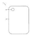
図1は1つの形態を説明するための図で、撮像モジュール10を具備する撮像装置1である携帯型端末1を平面視した図である。このように撮像モジュール10は、携帯型端末、パソコン、小型カメラ等に搭載されて撮像装置とすることができる。本形態の場合、図1に表れた側に窓が設けられ、ここから撮像モジュール10に光を取り込み、その反対側の画面により撮像モジュール10の操作が行われる。従って、撮像モジュール10は携帯型端末1を構成する筐体2に内臓されることにより配置される。
FIG. 1 is a diagram for explaining one embodiment, and is a diagram in plan view of a portable terminal 1 that is an imaging apparatus 1 including an
図2は撮像モジュール10の構成を説明する概念的な断面図である。図2からわかるように、撮像モジュール10は、レンズシート20、画像センサ11、及び画像処理装置12を有して構成されている。
FIG. 2 is a conceptual cross-sectional view illustrating the configuration of the
レンズシート20は、複数の単位レンズ要素24を含み、入射した光を画像センサ11上に集まるべき光線群に分解し、画像センサ11に出光する光学素子である。図2にはレンズシート20のひとつの断面が現れている。また、図3(a)にはレンズシート20の一部の斜視図、図3(b)にはレンズシート20を単位レンズ要素24側から平面視した図を示した。ここで図3(b)には破線で光吸収部23も併せて示している。
図4には図2の一部を拡大してレンズシート20の構造を説明するための図を表した。
The lens sheet 20 is an optical element that includes a plurality of
FIG. 4 shows a diagram for explaining the structure of the lens sheet 20 by enlarging a part of FIG.
レンズシート21は、シート面に平行な方向に沿って光吸収部23が格子状に形成されており、当該格子状の光吸収部23の間に光透過部22が配置されている。そして、レンズシート20の平面視で光透過部22となる位置に単位レンズ要素24が設けられている。また、本形態で光透過部22、及び光吸収部23は略台形又は長方形の断面を有している。
In the lens sheet 21,
光透過部22は光を透過させることを主要の機能とする部位であり、本形態では図2、図4に表れるように断面において、一方のシート面側に長い下底、その反対側である他方のシート面側に短い上底を有する略台形、又は長方形の断面形状を有する要素である。光透過部22は、格子状である光吸収部23の間に配置されており、光吸収部24に囲まれるように構成されている。従って、光透過部22は、頂部を除外した四角錐、又は四角柱状である。
なお、本形態では隣り合う光透過部22は長い下底側で連結され、土台部25とされている。土台部25は可能な限り薄いことが好ましい。これにより迷光を抑制することができ、高い画質を得ることができる。
The
In the present embodiment, the adjacent
光透過部22は屈折率がNtとされている。屈折率Ntの値は特に限定されることはないが、屈折率Ntは1.38以上、1.60以下であることが好ましい。屈折率が1.38より小さい材料は入手性に問題を生じる虞があり、屈折率が1.60より大きくなると割れが発生しやすい材料となる場合が多い。
The
このような光透過部22は例えばウレタンアクリレート、ポリエステルアクリレート、エポキシアクリレート等の紫外線硬化型樹脂、電子線硬化型樹脂、ポリエチレンテレフタレート(PET)などの熱可塑性樹脂等、により形成することができる。
Such a
光吸収部23は光透過部22を囲むようにして格子状に配置された、光を吸収する部位である。そして光透過部22が台形断面の場合には光吸収部23も台形断面となり、光吸収部23の短い上底が光透過部22の下底側を向き、光吸収部23の長い下底が光透過部22の上底側となる。一方光透過部22が長方形断面の場合には光吸収部23も長方形断面となる。
光吸収部23は、屈折率がNrとされるとともに、光を吸収することができるように構成されている。具体的には屈折率がNrであるバインダーに光吸収粒子が分散される。屈折率Nrは、光透過部22の屈折率Nt以上の屈折率であることが好ましい。このように、光吸収部23の屈折率を光透過部22の屈折率以上とすることにより、光透過部22と光吸収部23との界面で全反射することなく光が光吸収部23に入り、適切に光を吸収することができる。
屈折率Nrの値は特に限定されることはなく、光透過部22と同様に考えることができる。
The
The
The value of the refractive index Nr is not particularly limited, and can be considered in the same manner as the
バインダーとして用いられる材料は特に限定されないが、例えば、ウレタン(メタ)アクリレート、ポリエステル(メタ)アクリレート、エポキシ(メタ)アクリレート、およびブタジエン(メタ)アクリレート等の光硬化型樹脂組成物を挙げることができる。 Although the material used as a binder is not specifically limited, For example, photocurable resin compositions, such as urethane (meth) acrylate, polyester (meth) acrylate, epoxy (meth) acrylate, and butadiene (meth) acrylate, can be mentioned. .
本形態で用いられる光吸収粒子は、樹脂微粒子と、その樹脂微粒子の表面を被覆する色材層とからなる。 The light absorbing particles used in this embodiment are composed of resin fine particles and a color material layer covering the surface of the resin fine particles.
樹脂微粒子としては、メラミンビーズ、アクリルビーズ、アクリル−スチレンビーズ、ポリカーボネートビーズ、ポリエチレンビーズ、ポリスチレンビーズ、塩ビビーズ等、特に制限されることなく使用することができる。その中でも特に、アクリル架橋重合体、スチレン架橋重合体、またはアクリル−スチレン共重合体を好適に使用することが可能である。
樹脂微粒子は、透明なものも使用できるが、顔料または染料等で着色された樹脂を用いることが好ましく、必要に応じて特定の波長を選択的に吸収するものであってよいが、好ましくは黒色に着色された樹脂微粒子が用いられる。
As the resin fine particles, melamine beads, acrylic beads, acrylic-styrene beads, polycarbonate beads, polyethylene beads, polystyrene beads, polyvinyl chloride beads and the like can be used without particular limitation. Among these, an acrylic cross-linked polymer, a styrene cross-linked polymer, or an acrylic-styrene copolymer can be preferably used.
The resin fine particles may be transparent, but it is preferable to use a resin colored with a pigment or a dye, which may selectively absorb a specific wavelength as necessary, but preferably black. Colored resin fine particles are used.
色材層を構成して樹脂微粒子の表面を被覆する色材としては、光を吸収するものであれば特に制限されることなく使用することができ、着色されたフィラーやカーボンブラックを挙げることができる。
着色フィラーとしては、例えば、ポリマーに顔料を分散させた着色フィラーを好適に使用することができ、例えば、メタクリル酸メチルやスチレン等のモノマーに顔料を添加し、重合して得られた樹脂等を好適に使用することができる。顔料としては、公知の有機系顔料や無機系顔料を使用でき、例えば、カーボンブラック、アニリンブラック、ペリレンブラック等の有機系黒色顔料や、銅、鉄、クロム、マンガン、コバルト等を含有した無機系黒色顔料やチタンブラック等を好適に使用することができる。
カーボンブラックは、平均粒子径が10nm以上500nm以下のものを好適に使用することができ、例えば、ファーネスブラック、アセチレンブラック、チャンネルブラック、サーマルブラック、カーボンナノチューブ、カーボンファイバー等が使用できる。また、市販のものを使用することもでき、例えば、HCFシリーズ、MCFシリーズ、RCFシリーズ、LFFシリーズ(いずれも三菱化学株式会社製)、バルカンシリーズ(キャボット社製)、ケッチェンシリーズ(ライオン株式会社製)等を好適に使用することができる。
The color material that constitutes the color material layer and covers the surface of the resin fine particles can be used without particular limitation as long as it absorbs light, and includes a colored filler and carbon black. it can.
As the colored filler, for example, a colored filler in which a pigment is dispersed in a polymer can be suitably used. For example, a resin obtained by adding a pigment to a monomer such as methyl methacrylate or styrene and polymerizing it can be used. It can be preferably used. As the pigment, known organic pigments and inorganic pigments can be used. For example, inorganic black pigments such as carbon black, aniline black, perylene black, and inorganic pigments containing copper, iron, chromium, manganese, cobalt, etc. A black pigment, titanium black, or the like can be preferably used.
Carbon black having an average particle diameter of 10 nm to 500 nm can be suitably used. For example, furnace black, acetylene black, channel black, thermal black, carbon nanotube, carbon fiber, and the like can be used. Commercially available products can also be used. For example, HCF series, MCF series, RCF series, LFF series (all manufactured by Mitsubishi Chemical Corporation), Vulcan series (made by Cabot Corporation), Ketjen series (Lion Corporation) Etc.) can be preferably used.
ここで、本形態の光吸収粒子は、その平均粒子径は1μm以上5μm以下であることが好ましい。ここで「平均粒子径」とは、光吸収粒子を100個電子顕微鏡で観察してその直径を計り、算術平均した直径を意味する。
また、バインダーと光吸収粒子との質量部の比は、バインダーが100質量部に対して、光吸収粒子の質量部が10以上20以下であることが好ましい。これにともなって、光吸収の観点から光吸収粒子の光学濃度が2.4以上4.7以下であることが好ましい。
Here, the light-absorbing particles of this embodiment preferably have an average particle size of 1 μm or more and 5 μm or less. Here, the “average particle diameter” means an arithmetic average diameter obtained by observing 100 light absorbing particles with an electron microscope and measuring the diameter.
Moreover, it is preferable that the ratio of the mass part of a binder and light absorption particle | grains is 10-20 mass parts of light absorption particles with respect to 100 mass parts of binders. Accordingly, the optical density of the light-absorbing particles is preferably 2.4 or more and 4.7 or less from the viewpoint of light absorption.
本形態では光透過部22と光吸収部23との界面(台形断面の脚部)が断面において一直線状となる例を示したが、これに限らず折れ線状、凸である曲面状、凹である曲面状等であってもよい。また、複数の光透過部22及び光吸収部23で断面形状が同じであってもよいし、必要に応じて所定の規則性を有して異なる断面形状であってもよい。
また、当該断面は必ずしも等脚台形である必要はなく、一方の脚と他方の脚とが線対称でなく、一方と他方とで傾斜角度や形状が異なるように構成してもよい。
In this embodiment, an example in which the interface (leg part of the trapezoidal cross section) between the light transmitting
Further, the cross section is not necessarily an isosceles trapezoid, and one leg and the other leg are not line-symmetric, and one and the other may be configured such that the inclination angle and shape are different.
次に単位レンズ要素24について説明する。単位レンズ要素24は、図2〜図4よりわかるように、本形態では断面で曲線部を有する凸状であり、土台部25の面のうち、該土台部25を挟んで、光透過部22とは反対側の面に配列されている。図3(a)、図3(b)からわかるように、単位レンズ要素24は各光透過部22に対応するように設けられおり、光透過部22と単位レンズ要素24とはレンズシート20を平面視して同じ位置になるように位置づけられる。
このレンズシート20の単位レンズ要素24はマイクロレンズとして効果を奏するように光を制御する。すなわち、レンズシート20を透過した光が単位レンズ要素24により画像センサ11の受光面に焦点を結ぶように集光される。従って、単位レンズ要素24の曲率半径Rや屈折率はこのように光を制御できるように決められている。
そのための単位レンズ要素24の断面形状は特に限定されることはなく、楕円の一部、円弧、及び多角形状であってもよく、これらが組み合わされた形状であってもよい。
Next, the
The
Therefore, the cross-sectional shape of the
また、単位レンズ要素24の表面には、反射防止機能を有する層が形成されてもよい。この層は、フッ化マグネシウムや二酸化ケイ素、フッ素系コーティング剤などのような反射防止機能を有する材料を所定の膜厚でコーティングすることにより形成することができる。
Further, a layer having an antireflection function may be formed on the surface of the
レンズシート20は、特に限定されることはないが、例えば次のように光透過部22、光吸収部23、及び単位レンズ要素24が形成される。図4に記号を付した。
光透過部22、光吸収部23、及び単位レンズ要素24の配列ピッチPは20μm以上180μm以下とすることが好ましい。
このとき、光透過部22のうち、単位レンズ要素24が配置された側とは反対側のピッチ方向(幅方向)の大きさDtは、20μm以上180μm以下が好ましい。また、単位レンズ要素24が配置された側とは反対側の面における光吸収部23のピッチ方向(幅方向)の大きさWは2μm以上30μm以下であることが好ましい。
単位レンズ要素24の幅方向の大きさDlも20μm以上180μm以下であることが好ましい。
The lens sheet 20 is not particularly limited. For example, the
The arrangement pitch P of the
In this case, among the
The size D 1 in the width direction of the
一方、レンズシート20の厚さTは、単位レンズ要素24の頂部から、その反対側の面までの距離であり、30μm以上480μm以下であることが好ましい。
このうち、光透過部22、及び光吸収部23の厚さT1は20μm以上470μm以下であることが好ましい。
土台部25の厚さT2は1μm以上50μm以下である。これにより、迷光や光透過部22に入射した光が、隣接する他の光透過部22側に進んでしまうことを抑制することができる。
そして単位レンズ要素24の厚さT3は、2μm以上40μm以下であることが好ましい。
On the other hand, the thickness T of the lens sheet 20 is the distance from the top of the
Among these, it is preferable that the thickness T 1 of the
The thickness T 2 of the
And the thickness T 3 of the
また、単位凸レンズ要素24の曲率半径Rは10μm以上180μm以下であることが好ましい。これにより光学密着を抑制することができる。曲率半径Rが10μmより小さいと単位レンズ要素24としての光学的効果(レンズとしての効果)を得られない。一方曲率半径Rが180μmよりも大きいと単位レンズ要素が平坦な形状に近くなり、光学密着が生じやすい。
さらに、光透過部22と光吸収部23との界面がシート面法線(厚さ方向)と成す角θは0度以上10度以下が好ましい。0度では光透過部及び光吸収部が断面において長方形となる。
The radius of curvature R of the unit
Furthermore, the angle θ formed by the interface between the
以上のようなレンズシート20は例えば次のように作製することができる。図5〜図7に説明のための図を示した。
はじめに光吸収部23を形成する。すなわち、図5からわかるように、光吸収部23の形状を転写することができる金型と基材30との間に、光吸収部を構成する硬化前の組成物を供給し、適切な方法により硬化させて第一の中間シート31を得る。この第一の中間シート31は基材30の一方の面に光吸収部23が形成されたシートである。なお、基材30は後で剥離するので、基材30の表面には剥離しやすい加工がなされていることが好ましい。
The lens sheet 20 as described above can be manufactured as follows, for example. The figure for description was shown in FIGS.
First, the
次に、図6に示したように、作製した第一の中間シート31の光吸収部23側から硬化する前の光透過部22を構成する組成物を供給する。これにより光吸収部23に囲まれた凹部に当該組成物を充填する。また、当該凹部を越えて組成物を供給することにより土台部も形成する。組成物の供給方法は特に限定されることはないが、インサート射出成型やインクジェット充填を挙げることができる。
その後、適切は方法で組成物を硬化させることにより光透過部22及び土台部25を形成し、第二の中間シート32を得る。この第二の中間シート32は基材30の一方の面に光吸収部23、光透過部22及び土台部25が形成されたシートである。
Next, as shown in FIG. 6, the composition which comprises the
Then, the
次に、図7に示したように作製した第二の中間シート32のうち土台部25が形成された部位に対して適切な位置に単位レンズ要素24を配置する。これは例えば、単位レンズ要素24を構成する硬化前の組成物をインクジェット方式で供給し、その後に適切な方法で硬化させることにより行うことができる。
Next, the
そして、基材30を剥離して、適切な大きさに裁断することによりレンズシート20を得る。なお、基材30の剥離は第二の中間シート32を得て単位レンズ要素24を形成する前に行ってもよい。
And the lens sheet 20 is obtained by peeling the
以上の方法によれば効率よくレンズシート20を作製することができる。また、この方法にれば、光吸収部に光吸収粒子を確実に適切な場所にのみ配置することができ、意図していない場所に光吸収粒子が残留などすることなどを防止することができる。 According to the above method, the lens sheet 20 can be produced efficiently. Further, according to this method, the light absorbing particles can be surely disposed only in an appropriate place in the light absorbing portion, and the light absorbing particles can be prevented from remaining in an unintended place. .
図2に戻って画像センサ11について説明する。画像センサ11は、受光面で受光した光を電気信号に変換して出力する、いわゆる光電変換素子を複数配列してなるセンサである。画像センサ11には、複数の素子が2次元方向に配列されており、各素子により、その素子に入射した光の強度を検出することができる。そしてこの各素子が各画素を形成する。
画像センサ11を構成する複数の素子は、画像センサ11の受光面である被写体側(レンズシート20側)の表面に2次元方向に配列されている。
このような画像センサ11を構成する素子としては例えばCCDやCMOSを挙げることができる。
Returning to FIG. 2, the
A plurality of elements constituting the
Examples of the elements constituting such an
画像処理装置12は、画像センサ11で得られた電気信号を受信して画像処理をして奥行情報等を生成する手段である。画像処理装置12は、いわゆる演算基板により形成されており、中央演算子(CPU)、ROM、RAM等を有して形成され、ROMに記憶されたプログラムに基づいて中央演算子で演算を行うことで画像処理を行う。
The
以上のような、レンズシート20、画像センサ11、及び画像処理装置12は例えば次のように組み合わされて撮像モジュール10とされている。すなわち、図2に示したように、図2の紙面左側の被写体にレンズシート20の単位レンズ要素24が向くようにレンズシート20を配置する。
The lens sheet 20, the
そして、画像センサ11と画像処理装置12とが電気的に接続されデータを通信することができるように構成されている。
The
撮像モジュール10には、上記に加えて赤外線遮蔽層や反射防止層を設けてもよい。これにより入射光量の向上や、赤外線(特に近赤外線)によるノイズの低減を図ることができる。
In addition to the above, the
以上のような撮像モジュール10を備える撮像装置1は例えば次のように作用する。
被写体からの光は撮像モジュール10のレンズシート20内に進み、単位レンズ要素24により集光される。また、光透過部22内をシート法線方向に対して大きな角度をなす方向に進む光の少なくとも一部は光吸収部23に入射して吸収される。レンズシート20を透過した光は画像センサ11の受光面で焦点を結ぶ。従って、画像センサ11の受光面上には、このマイクロレンズとして単位レンズ要素24により結像された像が、それぞれ重なることなく形成される。
The imaging device 1 including the
Light from the subject travels into the lens sheet 20 of the
本形態では、単位レンズ要素24の1つ1つに対して、画像センサ11の複数の素子のいずれかが対応するように配置されている。そして、撮影時には、各素子には、対応する単位レンズ要素24により分割された光が入射し、各素子により光の強度が検出される。また、各素子と、単位レンズ要素と、の関係から素子に入射した光の入射方向が検出可能となる。
このようにして得られた各素子が検出した入射光の強度及び入射方向の情報は、上記画像処理装置12により演算され、撮影後に焦点距離や被写界深度を変更した画像データを生成可能である。
In this embodiment, one of the plurality of elements of the
Information on the intensity and direction of incident light detected by each element obtained in this way is calculated by the
図8は、本形態の撮像モジュール10における画像センサ11の受光面上での結像の様子を説明する図である。
一般的に、ライトフィールドカメラでは、マイクロレンズアレイの1つのマイクロレンズに対して、画像センサ11の所定の領域内に位置する複数の素子が対応している。そして、それぞれのマイクロレンズによる像が、対応する領域内のみに投影されることが重要である。
このとき、例えば図8(b)に示したように、各マイクロレンズの像が隣の領域等に投影され、像が重なると、被写体面上で異なる位置と角度を有する光が同一の素子に入射するクロストークという現象が生じ、光の入射方向や強度を分解できなくなる。
これを解消するために、従来のライトフィールドカメラでは、マイクロレンズアレイよりも被写体側に結像レンズを設ける必要があった。
FIG. 8 is a diagram for explaining a state of image formation on the light receiving surface of the
In general, in a light field camera, a plurality of elements located in a predetermined region of the
At this time, for example, as shown in FIG. 8B, when the images of the respective microlenses are projected onto an adjacent region or the like and the images overlap, light having different positions and angles on the subject surface is applied to the same element. A phenomenon called incident crosstalk occurs, and the incident direction and intensity of light cannot be decomposed.
In order to solve this problem, in the conventional light field camera, it is necessary to provide an imaging lens closer to the subject side than the microlens array.
これに対して、本形態によれば、光吸収部23が備えられているので、領域外に進行しようとする光をここで吸収し、図8(a)に示したようにクロストークを生じさせることなく単位レンズ要素24により集光された光を画像センサ11の対応する領域の素子に入射させることができる。これにより素子は、入射光の強度と入射方向の情報を高精度で出力することができる。
On the other hand, according to the present embodiment, since the
従って、本形態によれば、結像レンズ等の他の光学系を必要とすることなく、撮像モジュールの厚さを薄く、軽量化を図ることができる。例えば画像処理装置、及び画像センサ以外の光学系において厚さを数10μm以上数100μm以下の程度に抑えることが可能となる。これにより、撮像装置の外観も向上させることができる。
また製造の観点からも、結像光学系が不要となるので製造コストを抑制することが可能となる。
Therefore, according to this embodiment, the thickness of the imaging module can be reduced and the weight can be reduced without requiring another optical system such as an imaging lens. For example, in the optical system other than the image processing apparatus and the image sensor, the thickness can be suppressed to several tens of μm to several hundreds of μm. Thereby, the external appearance of an imaging device can also be improved.
Further, from the viewpoint of manufacturing, the image forming optical system is not necessary, so that the manufacturing cost can be suppressed.
1 撮像装置
2 筐体
10 撮像モジュール
11 画像センサ
12 画像処理装置
20 レンズシート
22 光透過部
23 光吸収部
24 単位レンズ要素
25 土台部
DESCRIPTION OF SYMBOLS 1
Claims (3)
格子状に形成された光を吸収する光吸収部、及び、前記光吸収部に囲まれるように配置された光を透過する光透過部と、
シートの平面視で複数の前記光透過部のそれぞれと同じ位置に配置される複数の単位レンズ要素と、を備える、レンズシート。 A lens sheet disposed on the light receiving surface side of the image sensor,
A light absorbing portion that absorbs light formed in a lattice shape, and a light transmitting portion that transmits light disposed so as to be surrounded by the light absorbing portion;
A lens sheet comprising: a plurality of unit lens elements arranged at the same position as each of the plurality of light transmission parts in a plan view of the sheet.
前記レンズシートの一方側に配置された、複数の光電変換素子が配列された画像センサと、を備える撮像モジュール。 The lens sheet according to claim 1;
An image pickup module comprising: an image sensor arranged on one side of the lens sheet and arranged with a plurality of photoelectric conversion elements.
Priority Applications (1)
| Application Number | Priority Date | Filing Date | Title |
|---|---|---|---|
| JP2016016483A JP2017134365A (en) | 2016-01-29 | 2016-01-29 | Lens sheet, imaging module, and imaging device |
Applications Claiming Priority (1)
| Application Number | Priority Date | Filing Date | Title |
|---|---|---|---|
| JP2016016483A JP2017134365A (en) | 2016-01-29 | 2016-01-29 | Lens sheet, imaging module, and imaging device |
Publications (1)
| Publication Number | Publication Date |
|---|---|
| JP2017134365A true JP2017134365A (en) | 2017-08-03 |
Family
ID=59504853
Family Applications (1)
| Application Number | Title | Priority Date | Filing Date |
|---|---|---|---|
| JP2016016483A Pending JP2017134365A (en) | 2016-01-29 | 2016-01-29 | Lens sheet, imaging module, and imaging device |
Country Status (1)
| Country | Link |
|---|---|
| JP (1) | JP2017134365A (en) |
Cited By (1)
| Publication number | Priority date | Publication date | Assignee | Title |
|---|---|---|---|---|
| CN111902762A (en) * | 2018-02-07 | 2020-11-06 | 洛克希德·马丁公司 | All-optical element imaging system |
Citations (5)
| Publication number | Priority date | Publication date | Assignee | Title |
|---|---|---|---|---|
| JP2003139918A (en) * | 2001-11-01 | 2003-05-14 | Nippon Sheet Glass Co Ltd | Method for manufacturing resin erecting lens array |
| WO2005107243A1 (en) * | 2004-04-28 | 2005-11-10 | Matsushita Electric Industrial Co., Ltd. | Image pickup device and method for manufacturing fine lens array |
| WO2006101064A1 (en) * | 2005-03-24 | 2006-09-28 | Matsushita Electric Industrial Co., Ltd. | Imaging device and lens array used therein |
| KR20140127588A (en) * | 2013-04-25 | 2014-11-04 | 삼성전기주식회사 | Camera module |
| KR101519588B1 (en) * | 2014-12-05 | 2015-05-12 | (주)스마트전자 | mobile terminal, camera module, printed circuit board for camera module and method for manufacturing thereof |
-
2016
- 2016-01-29 JP JP2016016483A patent/JP2017134365A/en active Pending
Patent Citations (6)
| Publication number | Priority date | Publication date | Assignee | Title |
|---|---|---|---|---|
| JP2003139918A (en) * | 2001-11-01 | 2003-05-14 | Nippon Sheet Glass Co Ltd | Method for manufacturing resin erecting lens array |
| WO2005107243A1 (en) * | 2004-04-28 | 2005-11-10 | Matsushita Electric Industrial Co., Ltd. | Image pickup device and method for manufacturing fine lens array |
| US20090141361A1 (en) * | 2004-04-28 | 2009-06-04 | Matsushita Electric Indstrial Co., Ltd. | Imaging Apparatus and Method for Manufacturing Microlens Array |
| WO2006101064A1 (en) * | 2005-03-24 | 2006-09-28 | Matsushita Electric Industrial Co., Ltd. | Imaging device and lens array used therein |
| KR20140127588A (en) * | 2013-04-25 | 2014-11-04 | 삼성전기주식회사 | Camera module |
| KR101519588B1 (en) * | 2014-12-05 | 2015-05-12 | (주)스마트전자 | mobile terminal, camera module, printed circuit board for camera module and method for manufacturing thereof |
Cited By (4)
| Publication number | Priority date | Publication date | Assignee | Title |
|---|---|---|---|---|
| CN111902762A (en) * | 2018-02-07 | 2020-11-06 | 洛克希德·马丁公司 | All-optical element imaging system |
| JP2021513271A (en) * | 2018-02-07 | 2021-05-20 | ロッキード マーティン コーポレイションLockheed Martin Corporation | Plenoptic Cellular Imaging System |
| JP7077411B2 (en) | 2018-02-07 | 2022-05-30 | ロッキード マーティン コーポレイション | Plenoptic Cellular Imaging System |
| CN111902762B (en) * | 2018-02-07 | 2022-12-09 | 洛克希德·马丁公司 | All-optical element imaging system |
Similar Documents
| Publication | Publication Date | Title |
|---|---|---|
| US10566365B2 (en) | Image sensor | |
| US7894139B2 (en) | Imaging apparatus and method for manufacturing microlens array | |
| US20090185291A1 (en) | Lens barrel and image pickup unit | |
| US20160141321A1 (en) | Image sensor | |
| KR102507207B1 (en) | Image Sensor Including A Passing Filter Having A Lower Refractive Index | |
| JP2023168388A (en) | Lens array, imaging module, and imaging apparatus | |
| US20160363673A1 (en) | Method of fabricating integrated digital x-ray image sensor, and integrated digital x-ray image sensor using the same | |
| JP6878817B2 (en) | Imaging module, imaging device | |
| KR102614907B1 (en) | Image sensor and method to produce image sensor | |
| JP2017134365A (en) | Lens sheet, imaging module, and imaging device | |
| JP6910105B2 (en) | Lens sheet, imaging module, and imaging device | |
| JP6686349B2 (en) | Imaging module, imaging device | |
| JP2017134364A (en) | Lens sheet, imaging module, and imaging device | |
| JP6686534B2 (en) | Lens sheet, imaging module, and imaging device | |
| JP2017146527A (en) | Imaging module and imaging apparatus | |
| JP6701716B2 (en) | Lens sheet, imaging module, imaging device | |
| JP6627526B2 (en) | Imaging module, imaging device | |
| JP6693086B2 (en) | Imaging module, imaging device | |
| JP6750216B2 (en) | Imaging module, imaging device | |
| JP7047417B2 (en) | Lens sheet unit, image pickup module, image pickup device | |
| JP6589464B2 (en) | Imaging module, imaging device | |
| CN104950359A (en) | Optical device, original plate, method of manufacturing original plate, and imaging apparatus | |
| JP2007304189A (en) | Method of manufacturing image recording medium | |
| JP2019128509A (en) | Lens sheet unit, and method for manufacturing lens sheet unit | |
| JP6724371B2 (en) | Imaging module, imaging device |
Legal Events
| Date | Code | Title | Description |
|---|---|---|---|
| A621 | Written request for application examination |
Free format text: JAPANESE INTERMEDIATE CODE: A621 Effective date: 20181128 |
|
| A977 | Report on retrieval |
Free format text: JAPANESE INTERMEDIATE CODE: A971007 Effective date: 20191126 |
|
| A131 | Notification of reasons for refusal |
Free format text: JAPANESE INTERMEDIATE CODE: A131 Effective date: 20191203 |
|
| A521 | Request for written amendment filed |
Free format text: JAPANESE INTERMEDIATE CODE: A523 Effective date: 20200127 |
|
| A02 | Decision of refusal |
Free format text: JAPANESE INTERMEDIATE CODE: A02 Effective date: 20200707 |