JP2017118791A - Power feeding control device - Google Patents

Power feeding control device Download PDF

Info

Publication number
JP2017118791A
JP2017118791A JP2015254883A JP2015254883A JP2017118791A JP 2017118791 A JP2017118791 A JP 2017118791A JP 2015254883 A JP2015254883 A JP 2015254883A JP 2015254883 A JP2015254883 A JP 2015254883A JP 2017118791 A JP2017118791 A JP 2017118791A
Authority
JP
Japan
Prior art keywords
voltage
circuit
output
resistance value
load
Prior art date
Legal status (The legal status is an assumption and is not a legal conclusion. Google has not performed a legal analysis and makes no representation as to the accuracy of the status listed.)
Withdrawn
Application number
JP2015254883A
Other languages
Japanese (ja)
Other versions
JP2017118791A5 (en
Inventor
佳祐 眞瀬
Keisuke Mase
佳祐 眞瀬
佑樹 杉沢
Yuki Sugisawa
佑樹 杉沢
康太 小田
Kota Oda
康太 小田
峻一 澤野
Shunichi Sawano
峻一 澤野
Current Assignee (The listed assignees may be inaccurate. Google has not performed a legal analysis and makes no representation or warranty as to the accuracy of the list.)
Sumitomo Wiring Systems Ltd
AutoNetworks Technologies Ltd
Sumitomo Electric Industries Ltd
Original Assignee
Sumitomo Wiring Systems Ltd
AutoNetworks Technologies Ltd
Sumitomo Electric Industries Ltd
Priority date (The priority date is an assumption and is not a legal conclusion. Google has not performed a legal analysis and makes no representation as to the accuracy of the date listed.)
Filing date
Publication date
Application filed by Sumitomo Wiring Systems Ltd, AutoNetworks Technologies Ltd, Sumitomo Electric Industries Ltd filed Critical Sumitomo Wiring Systems Ltd
Priority to JP2015254883A priority Critical patent/JP2017118791A/en
Priority to CN201680073574.9A priority patent/CN108370155A/en
Priority to EP16878765.3A priority patent/EP3396805A4/en
Priority to US15/778,377 priority patent/US20180358806A1/en
Priority to PCT/JP2016/088112 priority patent/WO2017110878A1/en
Publication of JP2017118791A publication Critical patent/JP2017118791A/en
Publication of JP2017118791A5 publication Critical patent/JP2017118791A5/ja
Withdrawn legal-status Critical Current

Links

Images

Classifications

    • HELECTRICITY
    • H02GENERATION; CONVERSION OR DISTRIBUTION OF ELECTRIC POWER
    • H02HEMERGENCY PROTECTIVE CIRCUIT ARRANGEMENTS
    • H02H9/00Emergency protective circuit arrangements for limiting excess current or voltage without disconnection
    • H02H9/02Emergency protective circuit arrangements for limiting excess current or voltage without disconnection responsive to excess current
    • H02H9/025Current limitation using field effect transistors
    • GPHYSICS
    • G05CONTROLLING; REGULATING
    • G05FSYSTEMS FOR REGULATING ELECTRIC OR MAGNETIC VARIABLES
    • G05F1/00Automatic systems in which deviations of an electric quantity from one or more predetermined values are detected at the output of the system and fed back to a device within the system to restore the detected quantity to its predetermined value or values, i.e. retroactive systems
    • G05F1/10Regulating voltage or current
    • G05F1/46Regulating voltage or current wherein the variable actually regulated by the final control device is dc
    • G05F1/56Regulating voltage or current wherein the variable actually regulated by the final control device is dc using semiconductor devices in series with the load as final control devices
    • G05F1/565Regulating voltage or current wherein the variable actually regulated by the final control device is dc using semiconductor devices in series with the load as final control devices sensing a condition of the system or its load in addition to means responsive to deviations in the output of the system, e.g. current, voltage, power factor
    • G05F1/569Regulating voltage or current wherein the variable actually regulated by the final control device is dc using semiconductor devices in series with the load as final control devices sensing a condition of the system or its load in addition to means responsive to deviations in the output of the system, e.g. current, voltage, power factor for protection
    • G05F1/573Regulating voltage or current wherein the variable actually regulated by the final control device is dc using semiconductor devices in series with the load as final control devices sensing a condition of the system or its load in addition to means responsive to deviations in the output of the system, e.g. current, voltage, power factor for protection with overcurrent detector
    • HELECTRICITY
    • H02GENERATION; CONVERSION OR DISTRIBUTION OF ELECTRIC POWER
    • H02HEMERGENCY PROTECTIVE CIRCUIT ARRANGEMENTS
    • H02H3/00Emergency protective circuit arrangements for automatic disconnection directly responsive to an undesired change from normal electric working condition with or without subsequent reconnection ; integrated protection
    • H02H3/24Emergency protective circuit arrangements for automatic disconnection directly responsive to an undesired change from normal electric working condition with or without subsequent reconnection ; integrated protection responsive to undervoltage or no-voltage
    • H02H3/243Emergency protective circuit arrangements for automatic disconnection directly responsive to an undesired change from normal electric working condition with or without subsequent reconnection ; integrated protection responsive to undervoltage or no-voltage for DC systems
    • HELECTRICITY
    • H02GENERATION; CONVERSION OR DISTRIBUTION OF ELECTRIC POWER
    • H02JCIRCUIT ARRANGEMENTS OR SYSTEMS FOR SUPPLYING OR DISTRIBUTING ELECTRIC POWER; SYSTEMS FOR STORING ELECTRIC ENERGY
    • H02J7/00Circuit arrangements for charging or depolarising batteries or for supplying loads from batteries
    • H02J7/0029Circuit arrangements for charging or depolarising batteries or for supplying loads from batteries with safety or protection devices or circuits
    • H02J7/00304Overcurrent protection
    • HELECTRICITY
    • H02GENERATION; CONVERSION OR DISTRIBUTION OF ELECTRIC POWER
    • H02JCIRCUIT ARRANGEMENTS OR SYSTEMS FOR SUPPLYING OR DISTRIBUTING ELECTRIC POWER; SYSTEMS FOR STORING ELECTRIC ENERGY
    • H02J7/00Circuit arrangements for charging or depolarising batteries or for supplying loads from batteries
    • H02J7/0063Circuit arrangements for charging or depolarising batteries or for supplying loads from batteries with circuits adapted for supplying loads from the battery
    • HELECTRICITY
    • H02GENERATION; CONVERSION OR DISTRIBUTION OF ELECTRIC POWER
    • H02JCIRCUIT ARRANGEMENTS OR SYSTEMS FOR SUPPLYING OR DISTRIBUTING ELECTRIC POWER; SYSTEMS FOR STORING ELECTRIC ENERGY
    • H02J7/00Circuit arrangements for charging or depolarising batteries or for supplying loads from batteries
    • H02J7/007Regulation of charging or discharging current or voltage
    • H02J7/00712Regulation of charging or discharging current or voltage the cycle being controlled or terminated in response to electric parameters
    • HELECTRICITY
    • H03ELECTRONIC CIRCUITRY
    • H03KPULSE TECHNIQUE
    • H03K17/00Electronic switching or gating, i.e. not by contact-making and –breaking
    • H03K17/08Modifications for protecting switching circuit against overcurrent or overvoltage
    • H03K17/082Modifications for protecting switching circuit against overcurrent or overvoltage by feedback from the output to the control circuit
    • H03K17/0822Modifications for protecting switching circuit against overcurrent or overvoltage by feedback from the output to the control circuit in field-effect transistor switches
    • HELECTRICITY
    • H03ELECTRONIC CIRCUITRY
    • H03KPULSE TECHNIQUE
    • H03K17/00Electronic switching or gating, i.e. not by contact-making and –breaking
    • H03K17/18Modifications for indicating state of switch
    • HELECTRICITY
    • H02GENERATION; CONVERSION OR DISTRIBUTION OF ELECTRIC POWER
    • H02JCIRCUIT ARRANGEMENTS OR SYSTEMS FOR SUPPLYING OR DISTRIBUTING ELECTRIC POWER; SYSTEMS FOR STORING ELECTRIC ENERGY
    • H02J7/00Circuit arrangements for charging or depolarising batteries or for supplying loads from batteries
    • H02J7/007Regulation of charging or discharging current or voltage
    • H02J7/00712Regulation of charging or discharging current or voltage the cycle being controlled or terminated in response to electric parameters
    • H02J7/007182Regulation of charging or discharging current or voltage the cycle being controlled or terminated in response to electric parameters in response to battery voltage

Abstract

PROBLEM TO BE SOLVED: To provide a power feeding control device capable of preventing conduction of a rush current and an overcurrent with certainty.SOLUTION: In a power feeding control device 11, a control circuit 23 adjusts a voltage of a gate in a semiconductor transistor 20 to adjust a resistance value between a drain and a source of the semiconductor transistor 20. A controller 56 determines whether or not a voltage of the source detected by a voltage detector 21 is equal to or more than a reference voltage after the control circuit 23 reduces the resistance value between the drain and the source. In a case where the controller 56 determines that the voltage of the source is equal to or more than the reference voltage, the control circuit 23 reduces the resistance value between the drain and the source again. In a case where the controller 56 determines that the voltage of the source is less than the predetermined voltage, the control circuit 23 adjusts the resistance value between the drain and the source to be equal to or more than a resistance value at a time point when the determination is performed.SELECTED DRAWING: Figure 1

Description

本発明は、バッテリから負荷への給電を制御する給電制御装置に関する。   The present invention relates to a power supply control device that controls power supply from a battery to a load.

車両には、バッテリから容量性の負荷への電流経路に設けられたスイッチをオン又はオフに切替えることによって、負荷への給電を制御する給電制御装置が搭載されている。この給電制御装置において、負荷が有するキャパシタに蓄えられている電力が低い状態でスイッチをオフからオンに切替えた場合、バッテリと負荷との電圧差が大きく、かつ、スイッチの両端間の抵抗値が小さいため、バッテリから負荷へ一時的に大きな電流が流れる。この電流は、所謂、突入電流である。突入電流が流れた場合、例えば、負荷を構成する部品が焼損する虞がある。   The vehicle is equipped with a power supply control device that controls power supply to the load by switching on or off a switch provided in a current path from the battery to the capacitive load. In this power supply control device, when the switch is switched from OFF to ON while the power stored in the capacitor of the load is low, the voltage difference between the battery and the load is large, and the resistance value between both ends of the switch is Since it is small, a large current temporarily flows from the battery to the load. This current is a so-called inrush current. When an inrush current flows, for example, there is a possibility that parts constituting the load may burn out.

特許文献1には、突入電流の発生を防止する給電制御装置が開示されている。この給電制御装置では、スイッチの一端に、抵抗及び第2スイッチの直列回路の一端が接続され、スイッチの他端にこの直列回路の他端が接続されている。スイッチをオフからオンに切替える前に、第2のスイッチをオフからオンに切替える。これにより、電流が、バッテリから抵抗及び第2のスイッチを介して負荷に流れる。   Patent Document 1 discloses a power supply control device that prevents the occurrence of an inrush current. In this power supply control device, one end of a series circuit of a resistor and a second switch is connected to one end of the switch, and the other end of the series circuit is connected to the other end of the switch. Before switching the switch from off to on, the second switch is switched from off to on. Thereby, current flows from the battery to the load via the resistor and the second switch.

ここで、電流が抵抗を介して負荷に流れるため、負荷のキャパシタに蓄えられている電力が小さい場合であっても、突入電流が流れることはない。キャパシタに一定の電力が蓄えられた後、第2のスイッチをオフに切替え、スイッチをオンに切替える。これにより、直列回路の抵抗で電力が消費されることなく、スイッチを介して電力をバッテリから負荷に供給することができる。   Here, since the current flows to the load via the resistor, the inrush current does not flow even when the electric power stored in the capacitor of the load is small. After a certain amount of power is stored in the capacitor, the second switch is turned off and the switch is turned on. Thereby, electric power can be supplied from a battery to a load via a switch, without consuming electric power by resistance of a series circuit.

特開2004−135389号公報JP 2004-135389 A

特許文献1に記載の給電制御装置のように、突入電流が負荷に流れることを防止する給電制御装置として、半導体トランジスタ、例えばFET(Field Effect Transistor)を備える給電制御装置が考えられる。この給電制御装置では、バッテリの正極と負荷の一端との間に半導体トランジスタが接続され、バッテリの負極及び負荷の他端は接地されている。半導体トランジスタでは、バッテリから入力端に電流が入力され、入力された電流は出力端から負荷に出力される。半導体トランジスタの入力端及び出力端間の抵抗値は、半導体トランジスタの制御端、例えばFETのゲートの電圧を調整することによって調整される。このような給電制御装置では、半導体トランジスタの入力端及び出力端間の抵抗値を徐々に低下させる。これにより、負荷に突入電流が流れることが防止される。   As a power supply control device that prevents an inrush current from flowing into a load, as in the power supply control device described in Patent Document 1, a power supply control device including a semiconductor transistor, for example, an FET (Field Effect Transistor) is conceivable. In this power supply control device, a semiconductor transistor is connected between the positive electrode of the battery and one end of the load, and the negative electrode of the battery and the other end of the load are grounded. In the semiconductor transistor, current is input from the battery to the input terminal, and the input current is output from the output terminal to the load. The resistance value between the input terminal and the output terminal of the semiconductor transistor is adjusted by adjusting the voltage at the control terminal of the semiconductor transistor, for example, the gate of the FET. In such a power supply control device, the resistance value between the input end and the output end of the semiconductor transistor is gradually reduced. This prevents an inrush current from flowing through the load.

半導体トランジスタを介した負荷への給電を制御する給電制御装置には、通常、過電流が半導体トランジスタに流れることを防止する構成が設けられている。例えば、負荷に流れる電流が大きい程、高い電圧を出力する出力回路が設けられている。出力回路が出力した電圧が所定の電圧以上である場合、半導体トランジスタの入力端及び出力端間の抵抗値を上昇させる。これにより、所定の電流以上の電流が半導体トランジスタに流れることはなく、過電流が半導体トランジスタを流れることが防止される。   A power supply control device that controls power supply to a load via a semiconductor transistor is usually provided with a configuration that prevents an overcurrent from flowing through the semiconductor transistor. For example, an output circuit is provided that outputs a higher voltage as the current flowing through the load increases. When the voltage output from the output circuit is equal to or higher than a predetermined voltage, the resistance value between the input terminal and the output terminal of the semiconductor transistor is increased. As a result, current exceeding a predetermined current does not flow through the semiconductor transistor, and overcurrent is prevented from flowing through the semiconductor transistor.

しかしながら、出力回路が半導体トランジスタの出力端の電圧を分圧することによって、出力すべき電圧を生成するように構成されている場合において、半導体トランジスタの出力端の電圧が所定の電圧未満であるとき、出力回路は、所定の電圧を超える電圧を出力することはできない。   However, when the output circuit is configured to generate a voltage to be output by dividing the voltage at the output terminal of the semiconductor transistor, when the voltage at the output terminal of the semiconductor transistor is less than a predetermined voltage, The output circuit cannot output a voltage exceeding a predetermined voltage.

従って、負荷に給電すべく、半導体トランジスタの入力端及び出力端間の抵抗値を低下させている場合において、半導体トランジスタの出力端の電圧が所定の電圧未満である間に所定の電流以上の電流が流れても、半導体トランジスタの入力端及び出力端間の抵抗値を上昇させることはない。このような出力回路を備える給電制御装置には、過電流の通流を確実に防止することができないという問題がある。   Therefore, in the case where the resistance value between the input terminal and the output terminal of the semiconductor transistor is lowered to supply power to the load, a current higher than a predetermined current while the voltage at the output terminal of the semiconductor transistor is less than the predetermined voltage. Does not increase the resistance value between the input terminal and the output terminal of the semiconductor transistor. The power supply control device including such an output circuit has a problem that it is not possible to reliably prevent the overcurrent from flowing.

本発明は斯かる事情に鑑みてなされたものであり、その目的とするところは、突入電流及び過電流の通流を確実に防止することができる給電制御装置を提供することにある。   This invention is made | formed in view of such a situation, The place made into the objective is providing the electric power feeding control apparatus which can prevent the rush current and the flow of an overcurrent reliably.

本発明に係る給電制御装置は、入力端に入力された電流を出力端から容量性の負荷に出力する半導体トランジスタと、該半導体トランジスタの前記入力端及び出力端間の抵抗値を調整する調整部とを備え、該調整部が前記抵抗値を調整することによって前記負荷への給電を制御する給電制御装置において、前記出力端の電圧を検出する検出部と、前記調整部が前記抵抗値を低下させた後、前記検出部が検出した前記出力端の電圧が所定電圧以上である否かを判定する判定部とを備え、前記調整部は、該判定部によって、前記出力端の電圧が前記所定電圧以上であると判定された場合に前記抵抗値を再び低下させ、前記判定部によって、前記出力端の電圧が前記所定電圧未満であると判定された場合、前記抵抗値を、該判定部が判定を行った時点の前記抵抗値以上に調整することを特徴とする。   A power supply control device according to the present invention includes a semiconductor transistor that outputs current input to an input terminal to a capacitive load from an output terminal, and an adjustment unit that adjusts a resistance value between the input terminal and the output terminal of the semiconductor transistor A power supply control device that controls power supply to the load by adjusting the resistance value, and a detection unit that detects a voltage at the output terminal, and the adjustment unit reduces the resistance value. And a determination unit that determines whether or not the voltage at the output end detected by the detection unit is equal to or higher than a predetermined voltage, and the adjustment unit causes the voltage at the output end to be determined by the determination unit. When it is determined that the voltage is equal to or higher than the voltage, the resistance value is decreased again. When the determination unit determines that the voltage at the output terminal is less than the predetermined voltage, the determination unit determines the resistance value. When a judgment is made And adjusting said more than the resistance value of.

本発明にあっては、半導体トランジスタの入力端には、電流が例えば、バッテリから入力され、入力された電流は、半導体トランジスタの出力端から容量性の負荷に出力される。半導体トランジスタの入力端及び出力端間の抵抗値を徐々に上昇させることによって、半導体トランジスタに突入電流が通流することを確実に防止することが可能である。   In the present invention, current is input from, for example, a battery to the input end of the semiconductor transistor, and the input current is output from the output end of the semiconductor transistor to the capacitive load. By gradually increasing the resistance value between the input terminal and the output terminal of the semiconductor transistor, it is possible to reliably prevent an inrush current from flowing through the semiconductor transistor.

負荷に給電すべく、半導体トランジスタの入力端及び出力端間の抵抗値を低下させる。これにより、負荷が有するキャパシタに電力が蓄えられる。抵抗値を低下させた後、検出した出力端の電圧が所定電圧以上であるか否かを判定する。負荷の両端が短絡しており、半導体トランジスタに過電流が流れる可能性がある場合、出力端の電圧は、略ゼロVであるので所定電圧未満となる。負荷の両端が短絡していない場合、出力端の電圧は所定電圧以上となる。   In order to supply power to the load, the resistance value between the input terminal and the output terminal of the semiconductor transistor is reduced. Thereby, electric power is stored in the capacitor of the load. After decreasing the resistance value, it is determined whether or not the detected voltage at the output terminal is equal to or higher than a predetermined voltage. When both ends of the load are short-circuited and there is a possibility that an overcurrent flows through the semiconductor transistor, the voltage at the output end is substantially zero V, and thus becomes less than a predetermined voltage. When both ends of the load are not short-circuited, the voltage at the output end is equal to or higher than a predetermined voltage.

出力端の電圧が所定電圧以上であると判定した場合、半導体トランジスタの入力端及び出力端間の抵抗値を再び低下させ、負荷への給電を行う。出力端の電圧が所定電圧未満であると判定した場合、半導体トランジスタの入力端及び出力端間の抵抗値を、判定を行った時点の抵抗値以上に調整し、半導体トランジスタに過電流が通流することを確実に防止する。   When it is determined that the voltage at the output terminal is equal to or higher than the predetermined voltage, the resistance value between the input terminal and the output terminal of the semiconductor transistor is lowered again to supply power to the load. When it is determined that the voltage at the output terminal is less than the predetermined voltage, the resistance value between the input terminal and output terminal of the semiconductor transistor is adjusted to be equal to or higher than the resistance value at the time of determination, and overcurrent flows through the semiconductor transistor. Make sure to prevent it.

本発明に係る給電制御装置は、前記調整部は、前記判定部が判定を行う前に、前記抵抗値を低下させてから該抵抗値を上昇させ、前記判定部は、前記調整部が前記抵抗値を上昇させた後に判定を行うことを特徴とする。   In the power supply control device according to the present invention, the adjustment unit decreases the resistance value and then increases the resistance value before the determination unit makes a determination. The determination is performed after increasing the value.

本発明にあっては、半導体トランジスタの入力端及び出力端間の抵抗値を低下させて、負荷のキャパシタに電力を供給した後、抵抗値を上昇させ、電力の供給を停止する。その後、半導体トランジスタの出力端の電圧が所定電圧以上であるか否かを判定する。電力の供給を一旦、停止するため、負荷の両端が短絡している場合に電力が無駄に消費されることはない。   In the present invention, the resistance value between the input terminal and the output terminal of the semiconductor transistor is reduced and power is supplied to the capacitor of the load. Then, the resistance value is increased and the supply of power is stopped. Thereafter, it is determined whether or not the voltage at the output terminal of the semiconductor transistor is equal to or higher than a predetermined voltage. Since the supply of electric power is temporarily stopped, electric power is not wasted when both ends of the load are short-circuited.

本発明に係る給電制御装置は、前記負荷に流れる電流が大きい程、高い電圧を出力する出力回路を備え、前記調整部は、該出力回路が出力した電圧が閾値以上である場合に前記抵抗値を上昇させ、前記出力回路が出力する電圧の最大値は、前記出力端の電圧以下であり、該出力端の電圧の上昇と共に上昇することを特徴とする。   The power supply control device according to the present invention includes an output circuit that outputs a higher voltage as the current flowing through the load increases, and the adjustment unit has the resistance value when the voltage output by the output circuit is equal to or greater than a threshold value. The maximum value of the voltage output from the output circuit is equal to or lower than the voltage at the output terminal, and increases as the voltage at the output terminal increases.

本発明にあっては、出力回路が出力した電圧が閾値以上である場合、半導体トランジスタの入力端及び出力端間の抵抗値を上昇させる。半導体トランジスタの出力端の電圧が高い場合、出力回路が出力する電圧の最大値が大きいため、出力回路が出力した電圧に基づいて、抵抗値を上昇させる構成が適正に作用する。このため、過電流の通流が防止される。半導体トランジスタの出力端の電圧が低い場合、出力回路が出力する電圧の最大値が小さいため、出力回路が出力した電圧に基づいて、抵抗値を上昇させる構成が適正に作用しない。しかし、検出した出力端の電圧に基づいて行う抵抗値の調整によって、過電流の通流が防止される。   In the present invention, when the voltage output from the output circuit is equal to or higher than the threshold value, the resistance value between the input terminal and the output terminal of the semiconductor transistor is increased. When the voltage at the output terminal of the semiconductor transistor is high, the maximum value of the voltage output from the output circuit is large, so that the configuration for increasing the resistance value works properly based on the voltage output from the output circuit. For this reason, overcurrent flow is prevented. When the voltage at the output terminal of the semiconductor transistor is low, the maximum value of the voltage output from the output circuit is small, so that the configuration for increasing the resistance value based on the voltage output from the output circuit does not work properly. However, the adjustment of the resistance value based on the detected voltage at the output terminal prevents the overcurrent from flowing.

本発明によれば、突入電流及び過電流の通流を確実に防止することができる。   According to the present invention, inrush current and overcurrent can be reliably prevented.

実施の形態1における電源システムの要部構成を示すブロック図である。1 is a block diagram illustrating a configuration of a main part of a power supply system according to Embodiment 1. FIG. 出力回路の回路図である。It is a circuit diagram of an output circuit. 制御回路の回路図である。It is a circuit diagram of a control circuit. 制御部が実行する開始処理の手順を示すフローチャートである。It is a flowchart which shows the procedure of the start process which a control part performs. 給電制御装置の動作の一例を示すタイミングチャートである。It is a timing chart which shows an example of operation of a feed control device. 給電制御装置の動作の他例を示すタイミングチャートである。It is a timing chart which shows the other example of operation | movement of an electric power feeding control apparatus. 実施の形態2における制御部が実行する開始処理の手順を示すフローチャートである。10 is a flowchart illustrating a procedure of start processing executed by a control unit according to Embodiment 2. 給電制御装置の動作の一例を示すタイミングチャートである。It is a timing chart which shows an example of operation of a feed control device. 給電制御装置の動作の他例を示すタイミングチャートである。It is a timing chart which shows the other example of operation | movement of an electric power feeding control apparatus.

以下、本発明をその実施の形態を示す図面に基づいて詳述する。
(実施の形態1)
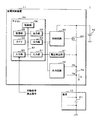
図1は実施の形態1における電源システム1の要部構成を示すブロック図である。電源システム1は、好適に車両に搭載されており、バッテリ10、給電制御装置11及び容量性の負荷12を備える。負荷12はキャパシタC1を有する。バッテリ10の正極と、負荷12が有するキャパシタC1の一端とは給電制御装置11に接続されている。バッテリ10の負極と、負荷12が有するキャパシタC1の他端とは接地されている。
Hereinafter, the present invention will be described in detail with reference to the drawings illustrating embodiments thereof.
(Embodiment 1)
FIG. 1 is a block diagram showing a main configuration of a power supply system 1 according to the first embodiment. The power supply system 1 is preferably mounted on a vehicle and includes a battery 10, a power supply control device 11, and a capacitive load 12. The load 12 has a capacitor C1. The positive electrode of the battery 10 and one end of the capacitor C1 included in the load 12 are connected to the power supply control device 11. The negative electrode of the battery 10 and the other end of the capacitor C1 included in the load 12 are grounded.

給電制御装置11には、負荷12の作動を指示する作動信号と、負荷12の動作の停止を指示する停止信号とが入力される。給電制御装置11は、入力された信号に基づいて、バッテリ10から負荷12への給電を制御する。   The power supply control device 11 receives an operation signal for instructing the operation of the load 12 and a stop signal for instructing the operation of the load 12 to stop. The power supply control device 11 controls power supply from the battery 10 to the load 12 based on the input signal.

負荷12は車両に搭載された電気機器である。負荷12は、バッテリ10から負荷12に給電されている場合に作動する。バッテリ10から負荷12への給電が停止されている場合、負荷12は動作を停止する。   The load 12 is an electric device mounted on the vehicle. The load 12 operates when power is supplied from the battery 10 to the load 12. When power supply from the battery 10 to the load 12 is stopped, the load 12 stops operating.

給電制御装置11は、半導体トランジスタ20、電圧検出部21、出力回路22、制御回路23、マイクロコンピュータ(以下、マイコンという)24及び抵抗Raを有する。半導体トランジスタ20において、ドレインはバッテリ10の正極に接続され、ソースは抵抗Raの一端に接続されている。抵抗Raの他端は、負荷12のキャパシタC1の一端に接続されている。半導体トランジスタ20のゲートは制御回路23に接続されている。制御回路23は、更に、バッテリ10の正極と、出力回路22と、マイコン24とに各別に接続されている。電圧検出部21は、半導体トランジスタ20のソースと、マイコン24とに各別に接続されている。出力回路22は、制御回路23の他に、抵抗Raの一端及び他端に各別に接続されている。   The power supply control device 11 includes a semiconductor transistor 20, a voltage detection unit 21, an output circuit 22, a control circuit 23, a microcomputer (hereinafter referred to as a microcomputer) 24, and a resistor Ra. In the semiconductor transistor 20, the drain is connected to the positive electrode of the battery 10, and the source is connected to one end of the resistor Ra. The other end of the resistor Ra is connected to one end of the capacitor C1 of the load 12. The gate of the semiconductor transistor 20 is connected to the control circuit 23. The control circuit 23 is further connected to the positive electrode of the battery 10, the output circuit 22, and the microcomputer 24. The voltage detector 21 is connected to the source of the semiconductor transistor 20 and the microcomputer 24 separately. In addition to the control circuit 23, the output circuit 22 is connected to one end and the other end of the resistor Ra separately.

バッテリ10の正極から、電流が半導体トランジスタ20のドレインに入力され、ドレインに入力された電流は、半導体トランジスタ20のソースから抵抗Raを介して負荷12に出力される。ドレイン及びソース夫々は入力端及び出力端として機能する。   From the positive electrode of the battery 10, a current is input to the drain of the semiconductor transistor 20, and the current input to the drain is output from the source of the semiconductor transistor 20 to the load 12 via the resistor Ra. The drain and the source function as an input terminal and an output terminal, respectively.

半導体トランジスタ20において、ドレイン及びソース間の抵抗値は、接地電位を基準としたゲートの電圧(以下、ゲート電圧という)に依存する。半導体トランジスタ20において、ゲート電圧が上昇した場合、ドレイン及びソース間の抵抗値は低下する。半導体トランジスタ20のゲートには、制御回路23によって電圧が印加される。制御回路23は、半導体トランジスタ20のゲート電圧を調整することによって、半導体トランジスタ20のドレイン及びソース間の抵抗値を調整する。制御回路23は調整部として機能する。   In the semiconductor transistor 20, the resistance value between the drain and the source depends on the gate voltage with respect to the ground potential (hereinafter referred to as the gate voltage). In the semiconductor transistor 20, when the gate voltage increases, the resistance value between the drain and the source decreases. A voltage is applied to the gate of the semiconductor transistor 20 by the control circuit 23. The control circuit 23 adjusts the resistance value between the drain and the source of the semiconductor transistor 20 by adjusting the gate voltage of the semiconductor transistor 20. The control circuit 23 functions as an adjustment unit.

制御回路23は、半導体トランジスタ20のゲート電圧を上昇させることによって、半導体トランジスタ20のドレイン及びソース間の抵抗値を低下させる。これにより、バッテリ10から半導体トランジスタ20及び抵抗Raを介して負荷12に給電される。
また、制御回路23は、半導体トランジスタ20のゲート電圧を低下させることによって、半導体トランジスタ20のドレイン及びソース間の抵抗値を上昇させる。これにより、バッテリ10から負荷12への給電が停止される。
以上のように、制御回路23は、半導体トランジスタ20のドレイン及びソース間の抵抗値を調整することによって、負荷12への給電を制御する。
The control circuit 23 decreases the resistance value between the drain and source of the semiconductor transistor 20 by increasing the gate voltage of the semiconductor transistor 20. As a result, power is supplied from the battery 10 to the load 12 via the semiconductor transistor 20 and the resistor Ra.
In addition, the control circuit 23 increases the resistance value between the drain and the source of the semiconductor transistor 20 by decreasing the gate voltage of the semiconductor transistor 20. Thereby, the power supply from the battery 10 to the load 12 is stopped.
As described above, the control circuit 23 controls the power supply to the load 12 by adjusting the resistance value between the drain and the source of the semiconductor transistor 20.

電圧検出部21は、接地電位を基準とした半導体トランジスタ20のソースの電圧(以下、ソース電圧という)を検出する。電圧検出部21は、検出したソース電圧を示す電圧情報をマイコン24に出力する。
出力回路22は電圧を制御回路23に出力する。出力回路22が制御回路23に出力する電圧は、抵抗Raを介して負荷12に流れる負荷電流Iaが上昇すると共に上昇するので、負荷電流Iaが大きい程高い。
The voltage detector 21 detects the source voltage of the semiconductor transistor 20 with reference to the ground potential (hereinafter referred to as source voltage). The voltage detector 21 outputs voltage information indicating the detected source voltage to the microcomputer 24.
The output circuit 22 outputs a voltage to the control circuit 23. The voltage output from the output circuit 22 to the control circuit 23 rises as the load current Ia flowing through the load 12 via the resistor Ra rises, so that the voltage increases as the load current Ia increases.

図2は出力回路22の回路図である。出力回路22は、PNP型のバイポーラトランジスタ30、差動増幅器31及び抵抗Rd,Reを有する。抵抗Reの一端は、半導体トランジスタ20のソースに接続されている。抵抗Reの他端は、バイポーラトランジスタ30のエミッタと、差動増幅器31のマイナス端子とに接続されている。差動増幅器31のプラス端子は抵抗Raの負荷12側の一端に接続されている。差動増幅器31の出力端はバイポーラトランジスタ30のベースに接続されている。バイポーラトランジスタ30のコレクタは、制御回路23と、抵抗Rdの一端とに接続されている。抵抗Rdの他端は接地されている。   FIG. 2 is a circuit diagram of the output circuit 22. The output circuit 22 includes a PNP-type bipolar transistor 30, a differential amplifier 31, and resistors Rd and Re. One end of the resistor Re is connected to the source of the semiconductor transistor 20. The other end of the resistor Re is connected to the emitter of the bipolar transistor 30 and the negative terminal of the differential amplifier 31. The positive terminal of the differential amplifier 31 is connected to one end of the resistor Ra on the load 12 side. The output terminal of the differential amplifier 31 is connected to the base of the bipolar transistor 30. The collector of the bipolar transistor 30 is connected to the control circuit 23 and one end of the resistor Rd. The other end of the resistor Rd is grounded.

半導体トランジスタ20のソースから出力された電流の大部分は、抵抗Raを介して負荷12に流れる。半導体トランジスタ20のソースから出力された電流の残りは、抵抗Re、バイポーラトランジスタ30及び抵抗Rdの順に流れる。バイポーラトランジスタ30において、電流はエミッタに入力され、エミッタに入力された電流はコレクタから抵抗Rdに出力される。   Most of the current output from the source of the semiconductor transistor 20 flows to the load 12 via the resistor Ra. The remainder of the current output from the source of the semiconductor transistor 20 flows in the order of the resistor Re, the bipolar transistor 30 and the resistor Rd. In bipolar transistor 30, current is input to the emitter, and the current input to the emitter is output from the collector to resistor Rd.

バイポーラトランジスタ30において、エミッタ及びコレクタ間の抵抗値は、接地電位を基準としたベースの電圧に依存する。バイポーラトランジスタ30のベースの電圧が上昇した場合、バイポーラトランジスタ30のエミッタ及びコレクタ間の抵抗値は上昇する。バイポーラトランジスタ30のベースには、差動増幅器31によって電圧が印加される。   In the bipolar transistor 30, the resistance value between the emitter and the collector depends on the voltage of the base with respect to the ground potential. When the voltage at the base of the bipolar transistor 30 increases, the resistance value between the emitter and collector of the bipolar transistor 30 increases. A voltage is applied to the base of the bipolar transistor 30 by a differential amplifier 31.

半導体トランジスタ20のソース電圧をVsと記載し、バイポーラトランジスタ30のエミッタ及びコレクタ間の抵抗値をrbと記載し、抵抗Rd,Re夫々の抵抗値をrd,reと記載する。バイポーラトランジスタ30のエミッタに入力されるエミッタ電流IeはVs/(rb+rd+re)で算出される。抵抗値rbが低下した場合、エミッタ電流Ieは上昇し、抵抗値rbが上昇した場合、エミッタ電流Ieは低下する。   The source voltage of the semiconductor transistor 20 is described as Vs, the resistance value between the emitter and the collector of the bipolar transistor 30 is described as rb, and the resistance values of the resistors Rd and Re are described as rd and re, respectively. The emitter current Ie input to the emitter of the bipolar transistor 30 is calculated as Vs / (rb + rd + re). When the resistance value rb decreases, the emitter current Ie increases, and when the resistance value rb increases, the emitter current Ie decreases.

差動増幅器31において、出力端からバイポーラトランジスタ30のベースに印加される電圧は、マイナス端子に印加されているエミッタ電圧Veと、プラス端子に印加されている負荷電圧Vaとに依存する。
差動増幅器31は、エミッタ電圧Veが負荷電圧Vaよりも高い場合、バイポーラトランジスタ30のベースに印加する電圧を低下させる。電圧の低下幅は、エミッタ電圧Veと負荷電圧Vaとの差が大きい程大きい。バイポーラトランジスタ30におけるベースの電圧の低下により、バイポーラトランジスタ30のエミッタ及びコレクタ間の抵抗値rbが低下する。結果、エミッタ電流Ieは上昇し、抵抗Reで生じる電圧降下の幅は上昇し、エミッタ電圧Veは低下する。エミッタ電圧Veは負荷電圧Vaに接近する。
In the differential amplifier 31, the voltage applied from the output terminal to the base of the bipolar transistor 30 depends on the emitter voltage Ve applied to the minus terminal and the load voltage Va applied to the plus terminal.
The differential amplifier 31 reduces the voltage applied to the base of the bipolar transistor 30 when the emitter voltage Ve is higher than the load voltage Va. The voltage decrease width increases as the difference between the emitter voltage Ve and the load voltage Va increases. The resistance value rb between the emitter and the collector of the bipolar transistor 30 decreases due to the decrease of the base voltage in the bipolar transistor 30. As a result, the emitter current Ie increases, the width of the voltage drop caused by the resistor Re increases, and the emitter voltage Ve decreases. The emitter voltage Ve approaches the load voltage Va.

また、差動増幅器31は、エミッタ電圧Veが負荷電圧Vaよりも低い場合、バイポーラトランジスタ30のベースに印加する電圧を上昇させる。電圧の上昇幅は、エミッタ電圧Veと負荷電圧Vaとの差が大きい程大きい。バイポーラトランジスタ30におけるベースの電圧の上昇により、バイポーラトランジスタ30のエミッタ及びコレクタ間の抵抗値rbが上昇する。結果、エミッタ電流Ieは低下し、抵抗Reで生じる電圧降下の幅は低下し、エミッタ電圧Veは上昇する。エミッタ電圧Veは負荷電圧Vaに接近する。   Further, the differential amplifier 31 increases the voltage applied to the base of the bipolar transistor 30 when the emitter voltage Ve is lower than the load voltage Va. The increase in voltage increases as the difference between the emitter voltage Ve and the load voltage Va increases. As the voltage at the base of the bipolar transistor 30 increases, the resistance value rb between the emitter and collector of the bipolar transistor 30 increases. As a result, the emitter current Ie decreases, the width of the voltage drop generated by the resistor Re decreases, and the emitter voltage Ve increases. The emitter voltage Ve approaches the load voltage Va.

以上のように、差動増幅器31は、エミッタ電圧Veが負荷電圧Vaと一致するように、半導体トランジスタ20のエミッタ及びコレクタ間の抵抗値rbを調整する。エミッタ電圧Veと負荷電圧Vaとが一致するので、下記の(1)式が成り立つ。
Vs−re×Ie=Vs−ra×Ia・・・(1)
ここで、raは、抵抗Raの抵抗値である。
(1)式を展開すると、下記の(2)式が成り立つ。
Ie=Ia×ra/re・・・(2)
As described above, the differential amplifier 31 adjusts the resistance value rb between the emitter and the collector of the semiconductor transistor 20 so that the emitter voltage Ve matches the load voltage Va. Since the emitter voltage Ve coincides with the load voltage Va, the following equation (1) is established.
Vs−re × Ie = Vs−ra × Ia (1)
Here, ra is the resistance value of the resistor Ra.
When the expression (1) is expanded, the following expression (2) is established.
Ie = Ia × ra / re (2)

例えば、抵抗値reが抵抗値raの1000倍である場合、エミッタ電流Ieは、負荷電流Iaの1000分の1である。このように、エミッタ電流Ieは、負荷電流Iaの所定数分の1であり、所定数は抵抗値ra,reによって決まる。   For example, when the resistance value re is 1000 times the resistance value ra, the emitter current Ie is 1/1000 of the load current Ia. Thus, the emitter current Ie is a predetermined number of the load current Ia, and the predetermined number is determined by the resistance values ra and re.

バイポーラトランジスタ30及び抵抗Rd,Reはソース電圧Vsを分圧し、分圧した電圧は制御回路23に出力される。出力回路22から制御回路23に出力される電圧は、rd×Ieである。エミッタ電流Ieは、前述したようにIa×ra/reで表されるので、出力回路22から制御回路23に出力される電圧は、Ia×ra×rd/reである。抵抗値ra,rd,reは定数であるため、出力回路22から制御回路23に出力される電圧は、負荷電流Iaに比例する。   The bipolar transistor 30 and the resistors Rd and Re divide the source voltage Vs, and the divided voltage is output to the control circuit 23. The voltage output from the output circuit 22 to the control circuit 23 is rd × Ie. Since the emitter current Ie is expressed by Ia × ra / re as described above, the voltage output from the output circuit 22 to the control circuit 23 is Ia × ra × rd / re. Since the resistance values ra, rd, and re are constants, the voltage output from the output circuit 22 to the control circuit 23 is proportional to the load current Ia.

ただし、出力回路22から制御回路23に出力される電圧が負荷電流Iaに比例する負荷電流Iaの範囲は制限されている。
エミッタ電流Ieは、バイポーラトランジスタ30のエミッタ及びコレクタ間の抵抗値rbが略ゼロΩとなった場合に最大となる。エミッタ電流Ieの最大値はVs/(rd+re)である。Vs/(rd+re)で表されるエミッタ電流Ieに対応する負荷電流IaはVs×re/(ra×(rd+re))である。
However, the range of the load current Ia in which the voltage output from the output circuit 22 to the control circuit 23 is proportional to the load current Ia is limited.
The emitter current Ie becomes maximum when the resistance value rb between the emitter and the collector of the bipolar transistor 30 becomes substantially zero Ω. The maximum value of the emitter current Ie is Vs / (rd + re). The load current Ia corresponding to the emitter current Ie represented by Vs / (rd + re) is Vs × re / (ra × (rd + re)).

従って、負荷電流IaがVs×re/(ra×(rd+re))を超えている場合、(2)式は成り立たない。この場合、負荷電流Iaに無関係に抵抗値rbは略ゼロΩであるため、出力回路22から制御回路23に出力される電圧は、一定であり、Vs×rd/(rd+re)で表される。従って、ソース電圧Vsが低い場合、出力回路22が適切な電圧を制御回路23に出力していない可能性がある。   Therefore, when the load current Ia exceeds Vs × re / (ra × (rd + re)), the equation (2) does not hold. In this case, since the resistance value rb is substantially zero Ω regardless of the load current Ia, the voltage output from the output circuit 22 to the control circuit 23 is constant and is expressed by Vs × rd / (rd + re). Therefore, when the source voltage Vs is low, the output circuit 22 may not output an appropriate voltage to the control circuit 23.

図1に示す制御回路23には、出力回路22から電圧が入力されると共に、マイコン24からローレベル電圧又はハイレベル電圧が入力される。制御回路23は、半導体トランジスタ20のゲートに電圧を印加する。制御回路23は、出力回路22及びマイコン24夫々から入力された電圧に基づいて半導体トランジスタ20のゲート電圧を調整する。   The control circuit 23 shown in FIG. 1 receives a voltage from the output circuit 22 and a low level voltage or a high level voltage from the microcomputer 24. The control circuit 23 applies a voltage to the gate of the semiconductor transistor 20. The control circuit 23 adjusts the gate voltage of the semiconductor transistor 20 based on the voltages input from the output circuit 22 and the microcomputer 24, respectively.

図3は制御回路23の回路図である。制御回路23は、コンパレータ40、ラッチ部41、反転器42、AND回路43、OR回路44、充電回路45、放電回路46、コンデンサC2及びダイオードD1,D2を有する。AND回路43及びOR回路44夫々は、2つの入力端子と、1つの出力端子とを有する。   FIG. 3 is a circuit diagram of the control circuit 23. The control circuit 23 includes a comparator 40, a latch unit 41, an inverter 42, an AND circuit 43, an OR circuit 44, a charging circuit 45, a discharging circuit 46, a capacitor C2, and diodes D1 and D2. Each of the AND circuit 43 and the OR circuit 44 has two input terminals and one output terminal.

コンパレータ40のプラス端子には、出力回路22、具体的には、バイポーラトランジスタ30のコレクタが接続されている。コンパレータ40のマイナス端子には参照電圧Vrが印加されている。参照電圧Vrは、一定であり、例えば、レギュレータを用いてバッテリ10の出力電圧から生成される。コンパレータ40の出力端子はラッチ部41の入力端子に接続されている。ラッチ部41の出力端子は、更に、反転器42の入力端子と、OR回路44の一方の入力端子とに接続されている。反転器42の出力端子はAND回路43の一方の入力端子に接続されている。AND回路43及びOR回路44夫々の他方の入力端子は、マイコン24に各別に接続されている。   The output circuit 22, specifically, the collector of the bipolar transistor 30 is connected to the plus terminal of the comparator 40. A reference voltage Vr is applied to the negative terminal of the comparator 40. The reference voltage Vr is constant and is generated from the output voltage of the battery 10 using a regulator, for example. The output terminal of the comparator 40 is connected to the input terminal of the latch unit 41. The output terminal of the latch unit 41 is further connected to the input terminal of the inverter 42 and one input terminal of the OR circuit 44. The output terminal of the inverter 42 is connected to one input terminal of the AND circuit 43. The other input terminal of each of the AND circuit 43 and the OR circuit 44 is connected to the microcomputer 24 separately.

AND回路43の出力端子は、充電回路45に接続されている。充電回路45は、更に、バッテリ10の正極と、ダイオードD1のアノードとに接続されている。充電回路45は接地されている。OR回路44の出力端子は、放電回路46に接続されている。放電回路46は、更に、ダイオードD2のカソードに接続されている。放電回路46は接地されている。   An output terminal of the AND circuit 43 is connected to the charging circuit 45. The charging circuit 45 is further connected to the positive electrode of the battery 10 and the anode of the diode D1. The charging circuit 45 is grounded. The output terminal of the OR circuit 44 is connected to the discharge circuit 46. The discharge circuit 46 is further connected to the cathode of the diode D2. The discharge circuit 46 is grounded.

ダイオードD1のカソードと、ダイオードD2のアノードとは、半導体トランジスタ20のゲートと、キャパシタC2の一端とに接続されている。キャパシタC2の他端は接地されている。   The cathode of the diode D1 and the anode of the diode D2 are connected to the gate of the semiconductor transistor 20 and one end of the capacitor C2. The other end of the capacitor C2 is grounded.

コンパレータ40は、出力回路22から制御回路23に出力された電圧が参照電圧Vr未満である場合、ローレベル電圧をラッチ部41に出力する。コンパレータ40は、出力回路22から制御回路23に出力された電圧が参照電圧Vr以上である場合、ハイレベル電圧をラッチ部41に出力する。   The comparator 40 outputs a low level voltage to the latch unit 41 when the voltage output from the output circuit 22 to the control circuit 23 is less than the reference voltage Vr. The comparator 40 outputs a high level voltage to the latch unit 41 when the voltage output from the output circuit 22 to the control circuit 23 is equal to or higher than the reference voltage Vr.

ラッチ部41は、コンパレータ40からローレベル電圧が入力されている間、ローレベル電圧を、反転器42の入力端子と、OR回路44の一方の入力端子とに出力する。ラッチ部41は、コンパレータ40から入力されている電圧がローレベル電圧からハイレベル電圧に切替わった場合、ハイレベル電圧を、反転器42の入力端子と、OR回路44の一方の入力端子とに出力する。コンパレータ40から入力されている電圧がローレベル電圧からハイレベル電圧に切替わった後においては、ラッチ部41は、コンパレータ40から入力される電圧に無関係にハイレベル電圧を出力し続ける。   While the low level voltage is input from the comparator 40, the latch unit 41 outputs the low level voltage to the input terminal of the inverter 42 and one input terminal of the OR circuit 44. When the voltage input from the comparator 40 is switched from the low level voltage to the high level voltage, the latch unit 41 applies the high level voltage to the input terminal of the inverter 42 and one input terminal of the OR circuit 44. Output. After the voltage input from the comparator 40 is switched from the low level voltage to the high level voltage, the latch unit 41 continues to output the high level voltage regardless of the voltage input from the comparator 40.

反転器42は、ラッチ部41からローレベル電圧が入力された場合、ハイレベル電圧をAND回路43の一方の入力端子に出力し、ラッチ部41からハイレベル電圧が入力された場合、ローレベル電圧をAND回路43の他方の入力端子に出力する。従って、出力回路22から制御回路23に出力される電圧が参照電圧Vr未満である間、AND回路43及びOR回路44夫々の一方の入力端子には、ハイレベル電圧及びローレベル電圧が入力される。出力回路22から制御回路23に出力される電圧が参照電圧Vr以上となった後においては、AND回路43及びOR回路44夫々の一方の入力端子には、ローレベル電圧及びハイレベル電圧が入力され続ける。   The inverter 42 outputs the high level voltage to one input terminal of the AND circuit 43 when the low level voltage is input from the latch unit 41, and the low level voltage when the high level voltage is input from the latch unit 41. Is output to the other input terminal of the AND circuit 43. Therefore, while the voltage output from the output circuit 22 to the control circuit 23 is less than the reference voltage Vr, a high level voltage and a low level voltage are input to one input terminal of each of the AND circuit 43 and the OR circuit 44. . After the voltage output from the output circuit 22 to the control circuit 23 becomes equal to or higher than the reference voltage Vr, a low level voltage and a high level voltage are input to one input terminal of each of the AND circuit 43 and the OR circuit 44. to continue.

AND回路43の他方の入力端子には、マイコン24からハイレベル電圧又はローレベル電圧が入力される。AND回路43は、反転器42から一方の端子にハイレベル電圧が入力されている場合、マイコン24から他方の入力端子に入力された電圧をそのまま充電回路45に出力する。AND回路43は、反転器42から一方の入力端子にローレベル電圧が入力されている場合、マイコン24から他方の入力端子に入力される電圧に無関係に、ローレベル電圧を充電回路45に出力する。   A high level voltage or a low level voltage is input from the microcomputer 24 to the other input terminal of the AND circuit 43. When a high level voltage is input from the inverter 42 to one terminal, the AND circuit 43 outputs the voltage input from the microcomputer 24 to the other input terminal to the charging circuit 45 as it is. When a low level voltage is input from the inverter 42 to one input terminal, the AND circuit 43 outputs the low level voltage to the charging circuit 45 regardless of the voltage input from the microcomputer 24 to the other input terminal. .

従って、出力回路22から制御回路23に出力される電圧が参照電圧Vr未満である間、マイコン24からAND回路43の他方の入力端子に入力された電圧がそのまま充電回路45に出力される。出力回路22から制御回路23に出力される電圧が参照電圧Vr以上となった後においては、マイコン24からAND回路43の他方の入力端子に入力される電圧に無関係にローレベル電圧を充電回路45に出力する。   Therefore, while the voltage output from the output circuit 22 to the control circuit 23 is less than the reference voltage Vr, the voltage input from the microcomputer 24 to the other input terminal of the AND circuit 43 is output to the charging circuit 45 as it is. After the voltage output from the output circuit 22 to the control circuit 23 becomes equal to or higher than the reference voltage Vr, the charging circuit 45 applies the low level voltage regardless of the voltage input from the microcomputer 24 to the other input terminal of the AND circuit 43. Output to.

充電回路45は、AND回路43からハイレベル電圧が入力された場合、バッテリ10を用いて一定の電圧を生成し、生成した電圧を、ダイオードD1を介してキャパシタC2の両端間に印加する。これにより、キャパシタC2は充電される。キャパシタC2の両端間の電圧が半導体トランジスタ20のゲートに印加される。キャパシタC2が充電されるにつれて、キャパシタC2の両端間の電圧が徐々に上昇し、半導体トランジスタ20のゲート電圧が徐々に上昇する。これにより、半導体トランジスタ20のドレイン及びソース間の抵抗値は徐々に低下する。
充電回路45は、AND回路43からローレベル電圧が入力された場合、動作を停止する。このとき、キャパシタC2は充電されることはない。
When a high level voltage is input from the AND circuit 43, the charging circuit 45 generates a constant voltage using the battery 10, and applies the generated voltage across the capacitor C2 via the diode D1. Thereby, the capacitor C2 is charged. A voltage across the capacitor C2 is applied to the gate of the semiconductor transistor 20. As the capacitor C2 is charged, the voltage across the capacitor C2 gradually increases, and the gate voltage of the semiconductor transistor 20 gradually increases. As a result, the resistance value between the drain and source of the semiconductor transistor 20 gradually decreases.
When the low level voltage is input from the AND circuit 43, the charging circuit 45 stops its operation. At this time, the capacitor C2 is not charged.

マイコン24は、ハイレベル電圧をAND回路43の他方の入力端子に出力することによって、充電回路45にキャパシタC2を充電させ、ローレベル電圧をAND回路43の他方の入力端子に出力することによって、充電回路45にキャパシタC2の充電を停止させる。   The microcomputer 24 outputs a high level voltage to the other input terminal of the AND circuit 43, thereby causing the charging circuit 45 to charge the capacitor C2, and outputs a low level voltage to the other input terminal of the AND circuit 43. The charging circuit 45 stops charging the capacitor C2.

OR回路44の他方の入力端子には、マイコン24からハイレベル電圧又はローレベル電圧が入力される。OR回路44は、ラッチ部41から一方の入力端子にローレベル電圧が入力されている場合、マイコン24から他方の入力端子に入力された電圧をそのまま放電回路46に出力する。OR回路44は、ラッチ部41から一方の入力端子にハイレベル電圧が入力されている場合、マイコン24から他方の入力端子に入力される電圧に無関係に、ハイレベル電圧を放電回路46に出力する。   A high level voltage or a low level voltage is input from the microcomputer 24 to the other input terminal of the OR circuit 44. When a low level voltage is input from the latch unit 41 to one input terminal, the OR circuit 44 outputs the voltage input from the microcomputer 24 to the other input terminal to the discharge circuit 46 as it is. The OR circuit 44 outputs the high level voltage to the discharge circuit 46 regardless of the voltage input from the microcomputer 24 to the other input terminal when the high level voltage is input from the latch unit 41 to the one input terminal. .

従って、出力回路22から制御回路23に出力される電圧が参照電圧Vr未満である間、マイコン24からOR回路44の他方の入力端子に入力された電圧がそのまま放電回路46に出力される。出力回路22から制御回路23に出力される電圧が参照電圧Vr以上となった後においては、マイコン24からOR回路44の他方の入力端子に入力される電圧に無関係にハイレベル電圧を放電回路46に出力する。   Accordingly, while the voltage output from the output circuit 22 to the control circuit 23 is less than the reference voltage Vr, the voltage input from the microcomputer 24 to the other input terminal of the OR circuit 44 is output to the discharge circuit 46 as it is. After the voltage output from the output circuit 22 to the control circuit 23 becomes equal to or higher than the reference voltage Vr, the high level voltage is applied to the discharge circuit 46 regardless of the voltage input from the microcomputer 24 to the other input terminal of the OR circuit 44. Output to.

放電回路46は、OR回路44からハイレベル電圧が入力された場合、キャパシタC2に放電させる。このとき、ダイオードD2のカソードは、放電回路46内の図示しない抵抗を介して接地されており、電流は、コンデンサC2からダイオードD2、放電回路46内の抵抗及び接地電位の順に流れる。キャパシタC2の放電により、キャパシタC2の両端間の電圧が低下し、半導体トランジスタ20のゲート電圧が低下する。これにより、半導体トランジスタ20のドレイン及びソース間の抵抗値は上昇する。
放電回路46は、OR回路44からローレベル電圧が入力された場合、動作を停止する。このとき、ダイオードD2のカソードは開放され、キャパシタC2は放電することはない。
When a high level voltage is input from the OR circuit 44, the discharge circuit 46 discharges the capacitor C2. At this time, the cathode of the diode D2 is grounded via a resistor (not shown) in the discharge circuit 46, and the current flows from the capacitor C2 to the diode D2, the resistor in the discharge circuit 46, and the ground potential in this order. Due to the discharge of the capacitor C2, the voltage across the capacitor C2 decreases, and the gate voltage of the semiconductor transistor 20 decreases. As a result, the resistance value between the drain and source of the semiconductor transistor 20 increases.
The discharge circuit 46 stops its operation when a low level voltage is input from the OR circuit 44. At this time, the cathode of the diode D2 is opened, and the capacitor C2 is not discharged.

マイコン24は、ハイレベル電圧をOR回路44の他方の入力端子に出力することによって、放電回路46にキャパシタC2の放電を行わせ、ローレベル電圧をOR回路44の他方の入力端子に出力することによって、放電回路46にキャパシタC2の放電を停止させる。   The microcomputer 24 outputs the high level voltage to the other input terminal of the OR circuit 44, thereby causing the discharge circuit 46 to discharge the capacitor C2, and outputs the low level voltage to the other input terminal of the OR circuit 44. This causes the discharge circuit 46 to stop discharging the capacitor C2.

以上のように構成された制御回路23において、出力回路22から制御回路23に出力されている電圧が参照電圧Vr未満である間、充電回路45及び放電回路46夫々はマイコン24から入力される電圧に従って、充電及び放電を行う。更に、出力回路22から制御回路23に出力されている電圧が参照電圧Vr以上である場合、充電回路45は動作を停止し、放電回路46が作動する。これにより、半導体トランジスタ20のゲート電圧は低下し、半導体トランジスタ20のドレイン及びソース間の抵抗値は上昇する。結果、バッテリ10から負荷12への給電が遮断される。これにより、出力回路22から制御回路23に出力される電圧は参照電圧Vrを超えることはない。参照電圧Vrは閾値に相当する。   In the control circuit 23 configured as described above, while the voltage output from the output circuit 22 to the control circuit 23 is less than the reference voltage Vr, each of the charging circuit 45 and the discharging circuit 46 is a voltage input from the microcomputer 24. According to the above, charging and discharging are performed. Furthermore, when the voltage output from the output circuit 22 to the control circuit 23 is equal to or higher than the reference voltage Vr, the charging circuit 45 stops operating and the discharging circuit 46 operates. As a result, the gate voltage of the semiconductor transistor 20 decreases, and the resistance value between the drain and source of the semiconductor transistor 20 increases. As a result, power supply from the battery 10 to the load 12 is interrupted. Thereby, the voltage output from the output circuit 22 to the control circuit 23 does not exceed the reference voltage Vr. The reference voltage Vr corresponds to a threshold value.

前述したように、出力回路22から制御回路23に出力される電圧は、負荷電流Ia、及び、抵抗Ra,Rd,Reの抵抗値ra,rd,reを用いて、Ia×ra×rd/reで表される。このため、出力回路22から制御回路23に出力される電圧が参照電圧Vr以上であることは、負荷電流Iaが電流閾値Ith(=Vr×re/(ra×rd))以上であることを意味する。従って、給電制御装置11では、負荷電流Iaが電流閾値Ith以上である場合、マイコン24から制御回路23に入力される電圧に無関係にバッテリ10から負荷12への給電が遮断される。結果、負荷電流Iaが電流閾値Ithを超えることはなく、過電流が半導体トランジスタ20を流れることはない。   As described above, the voltage output from the output circuit 22 to the control circuit 23 is Ia × ra × rd / re using the load current Ia and the resistance values ra, rd, and re of the resistors Ra, Rd, and Re. It is represented by Therefore, the voltage output from the output circuit 22 to the control circuit 23 being equal to or higher than the reference voltage Vr means that the load current Ia is equal to or higher than the current threshold Ith (= Vr × re / (ra × rd)). To do. Therefore, in the power supply control device 11, when the load current Ia is equal to or greater than the current threshold value Ith, power supply from the battery 10 to the load 12 is interrupted regardless of the voltage input from the microcomputer 24 to the control circuit 23. As a result, the load current Ia does not exceed the current threshold value Ith, and no overcurrent flows through the semiconductor transistor 20.

前述したように、出力回路22から制御回路23に出力される電圧は、rd×Ieであり、エミッタ電流Ieの最大値はVs/(rd+re)である。従って、出力回路22から制御回路23に出力される電圧の最大値は、Vs×rd/(rd+re)である。このため、この最大値Vs×rd/(rd+re)が参照電圧Vr以上である場合にのみ、給電が適正に遮断される。   As described above, the voltage output from the output circuit 22 to the control circuit 23 is rd × Ie, and the maximum value of the emitter current Ie is Vs / (rd + re). Therefore, the maximum value of the voltage output from the output circuit 22 to the control circuit 23 is Vs × rd / (rd + re). For this reason, power supply is properly cut off only when the maximum value Vs × rd / (rd + re) is equal to or higher than the reference voltage Vr.

出力回路22から制御回路23に出力される電圧の最大値Vs×rd/(rd+re)が参照電圧Vr未満である場合、負荷電流Iaの大きさに無関係に、コンパレータ40はローレベル電圧をラッチ部41に出力し続ける。   When the maximum value Vs × rd / (rd + re) of the voltage output from the output circuit 22 to the control circuit 23 is less than the reference voltage Vr, the comparator 40 latches the low level voltage regardless of the magnitude of the load current Ia. Continue to output to 41.

出力回路22から制御回路23に出力される電圧の最大値Vs×rd/(rd+re)は、ソース電圧Vsの上昇と共に上昇する。更に、rd/(rd+re)<1が成り立つため、Vs×rd/(rd+re)<Vsが成り立つ。このため、出力回路22から制御回路23に出力される電圧の最大値Vs×rd/(rd+re)はソース電圧Vs未満である。   The maximum voltage Vs × rd / (rd + re) output from the output circuit 22 to the control circuit 23 increases as the source voltage Vs increases. Furthermore, since rd / (rd + re) <1 holds, Vs × rd / (rd + re) <Vs holds. For this reason, the maximum value Vs × rd / (rd + re) of the voltage output from the output circuit 22 to the control circuit 23 is less than the source voltage Vs.

キャパシタC2の両端間の電圧がゼロVである場合、半導体トランジスタ20のゲート電圧はゼロVであり、半導体トランジスタ20のドレイン及びソースは開放状態である。このとき、抵抗Raに電流が流れないため、ソース電圧Vsは、負荷12のキャパシタC1の両端間の電圧と略一致しており、低い。放電回路46の動作が停止している状態で充電回路45がキャパシタC2を充電した場合、前述したように、半導体トランジスタ20のドレイン及びソース間の抵抗値は徐々に低下する。半導体トランジスタ20のドレイン及びソース間の抵抗値が徐々に低下するにつれて、ソース電圧Vsは徐々に上昇する。   When the voltage across the capacitor C2 is zero V, the gate voltage of the semiconductor transistor 20 is zero V, and the drain and source of the semiconductor transistor 20 are open. At this time, since no current flows through the resistor Ra, the source voltage Vs is substantially equal to the voltage across the capacitor C1 of the load 12 and is low. When the charging circuit 45 charges the capacitor C2 while the operation of the discharging circuit 46 is stopped, the resistance value between the drain and source of the semiconductor transistor 20 gradually decreases as described above. As the resistance value between the drain and source of the semiconductor transistor 20 gradually decreases, the source voltage Vs gradually increases.

ここで、出力回路22が制御回路23に出力する電圧の最大値Vs×rd/(rd+re)が参照電圧Vr未満である間、即ち、ソース電圧VsがVr×(rd+re)/rd未満である間、負荷電流Iaが電流閾値Ith(=Vr×re/(ra×rd))以上である場合であっても、バッテリ10から負荷12への給電は遮断されない。
そこで、給電制御装置11では、マイコン24は、電圧検出部21から入力される電圧情報に基づいて、制御回路23の充電回路45及び放電回路46の動作を制御することによって、ソース電圧VsがVr×(rd+re)/rd未満である間に負荷電流Iaが過電流となることを防止する。
Here, while the maximum value Vs × rd / (rd + re) of the voltage output from the output circuit 22 to the control circuit 23 is less than the reference voltage Vr, that is, while the source voltage Vs is less than Vr × (rd + re) / rd. Even when the load current Ia is equal to or greater than the current threshold Ith (= Vr × re / (ra × rd)), the power supply from the battery 10 to the load 12 is not interrupted.
Therefore, in the power supply control device 11, the microcomputer 24 controls the operation of the charging circuit 45 and the discharging circuit 46 of the control circuit 23 based on the voltage information input from the voltage detection unit 21, so that the source voltage Vs is Vr. The load current Ia is prevented from becoming an overcurrent while being less than x (rd + re) / rd.

図1に示すマイコン24は、入力部50,51、出力部52,53、タイマ54、記憶部55及び制御部56を有する。これらはバス57に接続されている。入力部51は、更に、電圧検出部21に接続されている。出力部52は、更に、制御回路23のAND回路43の他方の入力端子に接続されている。出力部53は、更に、制御回路23のOR回路44の他方の入力端子に接続されている。   The microcomputer 24 illustrated in FIG. 1 includes input units 50 and 51, output units 52 and 53, a timer 54, a storage unit 55, and a control unit 56. These are connected to the bus 57. The input unit 51 is further connected to the voltage detection unit 21. The output unit 52 is further connected to the other input terminal of the AND circuit 43 of the control circuit 23. The output unit 53 is further connected to the other input terminal of the OR circuit 44 of the control circuit 23.

入力部50には、作動信号又は停止信号が入力される。入力部50は、作動信号又は停止信号が入力された場合、その旨を制御部56に通知する。
入力部51には、電圧検出部21から入力部51に電圧情報が入力される。電圧情報は、制御部56によって入力部51から取得される。制御部56が入力部51から取得した電圧情報が示すソース電圧は、制御部56が電圧情報を取得した時点に電圧検出部21が検出したソース電圧と略一致している。
An operation signal or a stop signal is input to the input unit 50. When the operation signal or the stop signal is input, the input unit 50 notifies the control unit 56 to that effect.
Voltage information is input to the input unit 51 from the voltage detection unit 21 to the input unit 51. The voltage information is acquired from the input unit 51 by the control unit 56. The source voltage indicated by the voltage information acquired by the control unit 56 from the input unit 51 substantially matches the source voltage detected by the voltage detection unit 21 when the control unit 56 acquires the voltage information.

出力部52は、制御回路23のAND回路43の他方の端子にハイレベル電圧又はローレベル電圧を出力している。出力部52は、制御部56の指示に従って、制御回路23のAND回路43の他方の端子に出力している電圧をハイレベル電圧又はローレベル電圧に切替える。
出力部53は、制御回路23のOR回路44の他方の端子にハイレベル電圧又はローレベル電圧を出力している。出力部53は、制御部56の指示に従って、制御回路23のOR回路44の他方の端子に出力している電圧をハイレベル電圧又はローレベル電圧に切替える。
タイマ54は、制御部56の指示に従って、計時の開始及び終了を行う。タイマ54が計時している計時時間は、制御部56によって、タイマ54から読み出される。タイマ54が計時している計時時間は、制御部56によってゼロにリセットされる。
The output unit 52 outputs a high level voltage or a low level voltage to the other terminal of the AND circuit 43 of the control circuit 23. The output unit 52 switches the voltage output to the other terminal of the AND circuit 43 of the control circuit 23 to a high level voltage or a low level voltage in accordance with an instruction from the control unit 56.
The output unit 53 outputs a high level voltage or a low level voltage to the other terminal of the OR circuit 44 of the control circuit 23. The output unit 53 switches the voltage output to the other terminal of the OR circuit 44 of the control circuit 23 to a high level voltage or a low level voltage in accordance with an instruction from the control unit 56.
The timer 54 starts and ends timing in accordance with instructions from the control unit 56. The time measured by the timer 54 is read from the timer 54 by the control unit 56. The time measured by the timer 54 is reset to zero by the control unit 56.

記憶部55は不揮発性のメモリである。記憶部55には制御プログラムが記憶されている。制御部56は、図示しないCPU(Central Processing Unit)を有し、記憶部55に記憶されている制御プログラムを実行することによって、バッテリ10から負荷12への給電を開始する給電開始処理と、バッテリ10から負荷12への給電を終了する給電終了処理とを実行する。   The storage unit 55 is a nonvolatile memory. The storage unit 55 stores a control program. The control unit 56 has a CPU (Central Processing Unit) (not shown), executes a control program stored in the storage unit 55, thereby starting power supply from the battery 10 to the load 12, and a battery A power supply end process for terminating power supply from 10 to the load 12 is executed.

図4は制御部56が実行する給電開始処理の手順を示すフローチャートである。制御部56は、入力部50に作動信号が入力された場合に給電開始処理を実行する。給電開始処理は、出力部52,53夫々が制御回路23のAND回路43及びOR回路44夫々の他方の端子にローレベル電圧を出力している状態、即ち、充電回路45及び放電回路46が動作を停止している状態で開始される。   FIG. 4 is a flowchart illustrating a procedure of power supply start processing executed by the control unit 56. The control unit 56 performs a power feeding start process when an operation signal is input to the input unit 50. In the power feeding start process, the output units 52 and 53 output low level voltages to the other terminals of the AND circuit 43 and OR circuit 44 of the control circuit 23, that is, the charging circuit 45 and the discharging circuit 46 operate. Is started in a stopped state.

まず、制御部56は、出力部52に指示して、出力部52が制御回路23に出力している電圧をハイレベル電圧に切替えさせることによって、充電回路45に制御回路23のキャパシタC2の充電を開始させる(ステップS1)。ステップS1が実行される時点では、負荷電流IaはゼロAであるので、出力回路22から制御回路23に出力している電圧は参照電圧Vr未満である。このため、出力部52がAND回路43の他方の入力端子に出力した電圧がAND回路43の出力端子からそのまま充電回路45に入力される。   First, the control unit 56 instructs the output unit 52 to switch the voltage output from the output unit 52 to the control circuit 23 to a high level voltage, thereby causing the charging circuit 45 to charge the capacitor C2 of the control circuit 23. Is started (step S1). Since the load current Ia is zero A when step S1 is executed, the voltage output from the output circuit 22 to the control circuit 23 is less than the reference voltage Vr. Therefore, the voltage output from the output unit 52 to the other input terminal of the AND circuit 43 is directly input to the charging circuit 45 from the output terminal of the AND circuit 43.

次に、制御部56は、タイマ54に指示して計時を開始させ(ステップS2)、タイマ54が計時している計時時間が充電時間以上であるか否かを判定する(ステップS3)。充電時間は、一定であり、予め記憶部55に記憶されている。制御部56は、計時時間が充電時間未満であると判定した場合(S3:NO)、ステップS3を再び実行し、計時時間が充電時間以上となるまで待機する。   Next, the controller 56 instructs the timer 54 to start measuring time (step S2), and determines whether or not the time measured by the timer 54 is equal to or longer than the charging time (step S3). The charging time is constant and is stored in the storage unit 55 in advance. When it is determined that the timed time is less than the charging time (S3: NO), the control unit 56 executes Step S3 again and waits until the timed time becomes equal to or longer than the charging time.

制御部56は、計時時間が充電時間以上であると判定した場合(S3:YES)、出力部52に指示して、出力部52が制御回路23に出力している電圧をローレベル電圧に切替えさせることによって、充電回路45にキャパシタC2の充電を終了させる(ステップS4)。計時時間が充電時間以上となった時点において、出力回路22が出力している電圧の最大値は参照電圧Vr未満であるため、コンパレータ40はローレベル電圧を出力し続けている。このため、ステップS4では、出力部52がAND回路43の他方の入力端子に出力した電圧がそのまま制御回路23の充電回路45に入力される。   When it is determined that the measured time is equal to or longer than the charging time (S3: YES), the control unit 56 instructs the output unit 52 to switch the voltage output from the output unit 52 to the control circuit 23 to the low level voltage. This causes the charging circuit 45 to finish charging the capacitor C2 (step S4). Since the maximum value of the voltage output from the output circuit 22 is less than the reference voltage Vr when the time measured becomes equal to or longer than the charging time, the comparator 40 continues to output a low level voltage. Therefore, in step S <b> 4, the voltage output from the output unit 52 to the other input terminal of the AND circuit 43 is input to the charging circuit 45 of the control circuit 23 as it is.

次に、制御部56は、出力部53に指示して、出力部53が制御回路23に出力している電圧をハイレベル電圧に切替えさせることによって、放電回路46にキャパシタC2の放電を開始させる(ステップS5)。これにより、半導体トランジスタ20のゲート電圧が低下し、半導体トランジスタ20のドレイン及びソース間の抵抗値が上昇する。   Next, the control unit 56 instructs the output unit 53 to switch the voltage output from the output unit 53 to the control circuit 23 to a high level voltage, thereby causing the discharge circuit 46 to start discharging the capacitor C2. (Step S5). As a result, the gate voltage of the semiconductor transistor 20 decreases, and the resistance value between the drain and source of the semiconductor transistor 20 increases.

次に、制御部56は、タイマ54が計時している計時時間をゼロにリセットし(ステップS6)、タイマ54が計時している計時時間が放電時間以上であるか否かを判定する(ステップS7)。放電時間は、一定であり、予め記憶部55に記憶されている。   Next, the control unit 56 resets the time measured by the timer 54 to zero (step S6), and determines whether or not the time measured by the timer 54 is equal to or longer than the discharge time (step S6). S7). The discharge time is constant and is stored in the storage unit 55 in advance.

制御部56は、計時時間が放電時間未満であると判定した場合(S7:NO)、ステップS7を再び実行し、計時時間が放電時間以上となるまで待機する。制御部56は、計時時間が放電時間以上であると判定した場合(S7:YES)、出力部53に指示して、出力部53が制御回路23に出力している電圧をローレベル電圧に切替えさせることによって、放電回路46にキャパシタC2の放電を終了させる(ステップS8)。制御部56は、ステップS8を実行した後、タイマ54に指示して計時を終了させる(ステップS9)。   When it is determined that the measured time is less than the discharge time (S7: NO), the control unit 56 executes Step S7 again and waits until the measured time becomes equal to or longer than the discharge time. When it is determined that the measured time is equal to or longer than the discharge time (S7: YES), the control unit 56 instructs the output unit 53 to switch the voltage output from the output unit 53 to the control circuit 23 to a low level voltage. This causes the discharge circuit 46 to finish discharging the capacitor C2 (step S8). After executing Step S8, the control unit 56 instructs the timer 54 to end time measurement (Step S9).

次に、制御部56は、電圧検出部21から入力部51に入力された電圧情報を入力部51から取得し(ステップS10)、取得した電圧情報が示すソース電圧が基準電圧以上であるか否かを判定する(ステップS11)。基準電圧は、一定であり、予め記憶部55に記憶されている。後述するように、ステップS11において、ソース電圧が基準電圧以上であることは負荷12のキャパシタC1の両端が短絡していないことを示し、ソース電圧が基準電圧未満であることは負荷12のキャパシタC1の両端が短絡していることを示す。   Next, the control unit 56 acquires voltage information input from the voltage detection unit 21 to the input unit 51 from the input unit 51 (step S10), and whether or not the source voltage indicated by the acquired voltage information is equal to or higher than the reference voltage. Is determined (step S11). The reference voltage is constant and is stored in the storage unit 55 in advance. As will be described later, in step S11, when the source voltage is equal to or higher than the reference voltage, both ends of the capacitor C1 of the load 12 are not short-circuited, and when the source voltage is less than the reference voltage, the capacitor C1 of the load 12 It shows that both ends of are short-circuited.

制御部56は、ソース電圧が基準電圧未満であると判定した場合(S11:NO)、負荷12のキャパシタC1の両端が短絡しているとして、給電開始処理を終了し、キャパシタC1の充電を再開することはない。
なお、制御部56は、ソース電圧が基準電圧未満であると判定した場合において、図示しない出力部にキャパシタC1の短絡を示す短絡信号を出力させ、その後、給電開始処理を終了してもよい。
When it is determined that the source voltage is less than the reference voltage (S11: NO), the control unit 56 determines that both ends of the capacitor C1 of the load 12 are short-circuited, ends the power supply start process, and resumes charging of the capacitor C1. Never do.
When determining that the source voltage is lower than the reference voltage, the control unit 56 may cause the output unit (not shown) to output a short circuit signal indicating a short circuit of the capacitor C1, and then terminate the power supply start process.

制御部56は、ソース電圧が基準電圧以上であると判定した場合(S11:YES)、ステップS1と同様に、充電回路45にキャパシタC2の充電を開始させる(ステップS12)。
制御部56は、ステップS11を実行した後、キャパシタC1の充電が継続している状態で給電開始処理を終了する。
When determining that the source voltage is equal to or higher than the reference voltage (S11: YES), the control unit 56 causes the charging circuit 45 to start charging the capacitor C2 (step S12), similarly to step S1.
After executing Step S11, the control unit 56 ends the power supply start process while the capacitor C1 is continuously charged.

制御部56は、入力部50に停止信号が入力された場合に、給電終了処理を実行する。給電終了処理では、制御部56は、出力部52,53に指示して、出力部52,53夫々が出力している電圧をローレベル電圧及びハイレベル電圧に切替える。これにより、充電回路45がキャパシタC1の充電を終了し、放電回路46がキャパシタC1の放電を開始する。制御部56は、放電回路46にキャパシタC1の放電を一定時間だけ行わせて、半導体トランジスタ20のゲート電圧がゼロVとなった後、出力部53に指示して、出力部53が制御部56に出力している電圧をローレベル電圧に切替えさせる。これにより、放電回路46が行っているキャパシタC1の放電が終了する。制御部56は、出力部53に指示して、出力部53が制御部56に出力している電圧をローレベル電圧に切替えさせ後、給電終了処理を終了する。   When the stop signal is input to the input unit 50, the control unit 56 performs a power supply end process. In the power supply end process, the control unit 56 instructs the output units 52 and 53 to switch the voltage output from each of the output units 52 and 53 to a low level voltage and a high level voltage. Thereby, the charging circuit 45 ends the charging of the capacitor C1, and the discharging circuit 46 starts discharging the capacitor C1. The control unit 56 causes the discharge circuit 46 to discharge the capacitor C1 for a certain period of time, and after the gate voltage of the semiconductor transistor 20 reaches zero V, the control unit 56 instructs the output unit 53 so that the output unit 53 controls the control unit 56. The voltage output to is switched to a low level voltage. Thereby, the discharge of the capacitor C1 performed by the discharge circuit 46 is completed. The control unit 56 instructs the output unit 53 to switch the voltage output from the output unit 53 to the control unit 56 to a low level voltage, and then ends the power supply termination process.

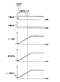
図5は、給電制御装置11の動作の一例を示すタイミングチャートである。図5には、充電回路45及び放電回路46夫々に入力されている電圧の推移と、ゲート電圧、負荷電流Ia及びソース電圧Vs夫々の推移とが示されている。これらの推移は、負荷12の両端が短絡していない場合における推移である。横軸は時間を示す。図5では、ハイレベル電圧を「H」で示し、ローレベル電圧を「L」で示している。   FIG. 5 is a timing chart illustrating an example of the operation of the power supply control device 11. FIG. 5 shows transitions of voltages input to the charging circuit 45 and the discharging circuit 46, and transitions of the gate voltage, the load current Ia, and the source voltage Vs, respectively. These transitions are transitions when both ends of the load 12 are not short-circuited. The horizontal axis indicates time. In FIG. 5, the high level voltage is indicated by “H” and the low level voltage is indicated by “L”.

前述したように、マイコン24の入力部50に作動信号が入力された場合、マイコン24の制御部56は給電開始処理を実行する。給電開始処理では、マイコン24は、まず、放電回路46に入力されている電圧をローレベル電圧に維持している状態で、充電回路45に入力されている電圧をハイレベル電圧に切替え、制御回路23の充電回路45にキャパシタC2の充電を開始させる。これにより、キャパシタC2の両端間の電圧、即ち、ゲート電圧が徐々に上昇し、半導体トランジスタ20のドレイン及びソース間の抵抗値が徐々に低下する。   As described above, when an operation signal is input to the input unit 50 of the microcomputer 24, the control unit 56 of the microcomputer 24 executes a power feeding start process. In the power supply start process, the microcomputer 24 first switches the voltage input to the charging circuit 45 to the high level voltage while maintaining the voltage input to the discharge circuit 46 at the low level voltage, and the control circuit 23 charging circuit 45 starts charging capacitor C2. As a result, the voltage across the capacitor C2, that is, the gate voltage gradually increases, and the resistance value between the drain and source of the semiconductor transistor 20 gradually decreases.

半導体トランジスタ20のドレイン及びソース間の抵抗値が低下した場合、バッテリ10から半導体トランジスタ20を介して負荷12に負荷電流Iaが流れる。半導体トランジスタ20のドレイン及びソース間の抵抗値が徐々に低下するにつれて、負荷電流Iaも徐々に上昇する。
以上のように、半導体トランジスタ20のドレイン及びソース間の抵抗値が徐々に低下するので、突入電流が半導体トランジスタ20を介して負荷12に流れることを確実に防止することができる。
When the resistance value between the drain and source of the semiconductor transistor 20 decreases, a load current Ia flows from the battery 10 to the load 12 via the semiconductor transistor 20. As the resistance value between the drain and source of the semiconductor transistor 20 gradually decreases, the load current Ia also gradually increases.
As described above, since the resistance value between the drain and source of the semiconductor transistor 20 gradually decreases, it is possible to reliably prevent an inrush current from flowing to the load 12 via the semiconductor transistor 20.

負荷12の両端が短絡していない限り、半導体トランジスタ20のドレイン及びソース間の抵抗値が徐々に低下するにつれて、半導体トランジスタ20のソース電圧Vsは徐々に上昇する。また、バッテリ10から負荷12への給電によって、負荷12のキャパシタC1が充電され、キャパシタC1の両端間の電圧も上昇する。   As long as both ends of the load 12 are not short-circuited, the source voltage Vs of the semiconductor transistor 20 gradually increases as the resistance value between the drain and source of the semiconductor transistor 20 gradually decreases. Further, the power supply from the battery 10 to the load 12 charges the capacitor C1 of the load 12, and the voltage across the capacitor C1 also increases.

充電回路45がキャパシタC2の充電を開始してから充電時間が経過した場合、マイコン24は、充電回路45に入力されている電圧をローレベル電圧に切替え、充電回路45にキャパシタC2の充電を終了させる。これにより、ゲート電圧、負荷電流Ia、ソース電圧、及び、キャパシタC1の両端間の電圧夫々の上昇は停止する。   When the charging time has elapsed since the charging circuit 45 started charging the capacitor C2, the microcomputer 24 switches the voltage input to the charging circuit 45 to a low level voltage, and the charging circuit 45 finishes charging the capacitor C2. Let As a result, the increase in the gate voltage, the load current Ia, the source voltage, and the voltage across the capacitor C1 is stopped.

次に、マイコン24は、放電回路46に入力されている電圧をローレベル電圧からハイレベル電圧に切替え、放電回路46にキャパシタC2の放電を開始させる。これにより、キャパシタC2の両端間の電圧が低下し、半導体トランジスタ20のゲート電圧は低下する。ゲート電圧の低下により、半導体トランジスタ20のドレイン及びソース間の抵抗値が上昇し、負荷電流Iaが低下する。負荷電流Iaの低下と共に、ソース電圧VsもキャパシタC1の両端間の電圧まで低下する。   Next, the microcomputer 24 switches the voltage input to the discharge circuit 46 from the low level voltage to the high level voltage, and causes the discharge circuit 46 to start discharging the capacitor C2. As a result, the voltage across the capacitor C2 decreases, and the gate voltage of the semiconductor transistor 20 decreases. As the gate voltage decreases, the resistance value between the drain and source of the semiconductor transistor 20 increases, and the load current Ia decreases. As the load current Ia decreases, the source voltage Vs also decreases to the voltage across the capacitor C1.

放電時間は、放電回路46が行う放電によって、キャパシタC2の両端間の電圧がゼロVとなるために必要な時間よりも十分に長い。このため、放電回路46に入力されている電圧がローレベル電圧からハイレベル電圧に切替わってから放電時間が経過した時点では、ゲート電圧はゼロVであり、半導体トランジスタ20のドレイン及びソースは開放状態である。放電時間が経過した時点において、抵抗Raに電流が流れていないため、ソース電圧VsはキャパシタC1の両端間の電圧と一致している。   The discharge time is sufficiently longer than the time necessary for the voltage across the capacitor C2 to become zero V due to the discharge performed by the discharge circuit 46. Therefore, the gate voltage is zero V and the drain and source of the semiconductor transistor 20 are open when the discharge time elapses after the voltage input to the discharge circuit 46 is switched from the low level voltage to the high level voltage. State. Since no current flows through the resistor Ra when the discharge time has elapsed, the source voltage Vs matches the voltage across the capacitor C1.

負荷12の両端が短絡されていない限り、作動信号が入力部50に入力されてから充電時間が経過するまでに、キャパシタC1の両端間の電圧は基準電圧Vb以上となっている。このため、負荷12の両端が短絡されていない限り、放電時間が経過した時点において、ソース電圧Vsは基準電圧Vb以上である。   As long as both ends of the load 12 are not short-circuited, the voltage between both ends of the capacitor C1 is equal to or higher than the reference voltage Vb until the charging time elapses after the operation signal is input to the input unit 50. For this reason, as long as both ends of the load 12 are not short-circuited, the source voltage Vs is equal to or higher than the reference voltage Vb when the discharge time has elapsed.

放電回路46が制御回路23のキャパシタC2の放電を終了した後、マイコン24の制御部56は、電圧検出部21から入力された電圧情報が示すソース電圧Vsが基準電圧Vb以上であるか否かを判定する。マイコン24は、制御部56によってソース電圧Vsが基準電圧Vb以上であると判定された場合、負荷12の両端が短絡していないとして、充電回路45に入力されている電圧をローレベル電圧からハイレベル電圧に切替え、マイコン24の制御部56は給電開始処理が終了する。制御部56は判定部として機能し、基準電圧Vbは所定電圧に相当する。   After the discharge circuit 46 finishes discharging the capacitor C2 of the control circuit 23, the control unit 56 of the microcomputer 24 determines whether or not the source voltage Vs indicated by the voltage information input from the voltage detection unit 21 is equal to or higher than the reference voltage Vb. Determine. When the control unit 56 determines that the source voltage Vs is equal to or higher than the reference voltage Vb, the microcomputer 24 determines that the both ends of the load 12 are not short-circuited and changes the voltage input to the charging circuit 45 from the low level voltage to the high level voltage. After switching to the level voltage, the control unit 56 of the microcomputer 24 ends the power supply start process. The control unit 56 functions as a determination unit, and the reference voltage Vb corresponds to a predetermined voltage.

この電圧の切替えにより、充電回路45は、制御回路23のキャパシタC2を再び充電し、半導体トランジスタ20のゲート電圧を上昇させ、半導体トランジスタ20のドレイン及びソース間の抵抗値を低下させる。これにより、バッテリ10から負荷12に給電され、負荷電流Ia及びソース電圧Vsは再び上昇する。
このとき、負荷12の両端は短絡していないため、出力回路22から制御回路23に出力している電圧の最大値が参照電圧Vr未満である間に、負荷電流Iaが電流閾値Ith(=Vr×re/(ra×rd))以上となることはない。
By switching the voltage, the charging circuit 45 recharges the capacitor C2 of the control circuit 23, increases the gate voltage of the semiconductor transistor 20, and decreases the resistance value between the drain and source of the semiconductor transistor 20. As a result, power is supplied from the battery 10 to the load 12, and the load current Ia and the source voltage Vs rise again.
At this time, since both ends of the load 12 are not short-circuited, while the maximum value of the voltage output from the output circuit 22 to the control circuit 23 is less than the reference voltage Vr, the load current Ia is the current threshold value Ith (= Vr No more than xre / (ra * rd)).

制御回路23において、充電回路45がコンデンサC2に出力している電圧と、コンデンサC2の両端間の電圧とが一致した場合、ゲート電圧の上昇は停止し、ゲート電圧は安定する。これにより、負荷電流Ia及びソース電圧Vsの上昇も停止し、負荷電流Ia及びソース電圧Vsは安定する。   In the control circuit 23, when the voltage output from the charging circuit 45 to the capacitor C2 matches the voltage across the capacitor C2, the increase in the gate voltage is stopped and the gate voltage is stabilized. Thereby, the rise of the load current Ia and the source voltage Vs is also stopped, and the load current Ia and the source voltage Vs are stabilized.

図6は、給電制御装置11の動作の他例を示すタイミングチャートである。図6には、図5と同様に、充電回路45及び放電回路46夫々に入力されている電圧の推移と、ゲート電圧、負荷電流Ia及びソース電圧Vs夫々の推移とが示されている。これらの推移は、負荷12の両端が短絡している場合における推移である。横軸は時間を示す。図6でも、ハイレベル電圧を「H」で示し、ローレベル電圧を「L」で示している。   FIG. 6 is a timing chart showing another example of the operation of the power supply control device 11. FIG. 6 shows transitions of voltages input to the charging circuit 45 and the discharging circuit 46 and transitions of the gate voltage, the load current Ia, and the source voltage Vs, respectively, as in FIG. These transitions are transitions when both ends of the load 12 are short-circuited. The horizontal axis indicates time. Also in FIG. 6, the high level voltage is indicated by “H”, and the low level voltage is indicated by “L”.

前述したように、マイコン24の入力部50に作動信号が入力された場合、マイコン24の制御部56は給電開始処理を実行する。マイコン24は、放電回路46に入力されている電圧をローレベル電圧に維持している状態で、制御回路23の充電回路45に入力されている電圧をハイレベル電圧に切替え、充電回路45にキャパシタC2の充電を開始させる。これにより、キャパシタC2の両端間の電圧が徐々に上昇し、半導体トランジスタ20のドレイン及びソース間の抵抗値が徐々に低下する。   As described above, when an operation signal is input to the input unit 50 of the microcomputer 24, the control unit 56 of the microcomputer 24 executes a power feeding start process. The microcomputer 24 switches the voltage input to the charging circuit 45 of the control circuit 23 to the high level voltage in a state where the voltage input to the discharging circuit 46 is maintained at the low level voltage. Start charging C2. As a result, the voltage across the capacitor C2 gradually increases, and the resistance value between the drain and source of the semiconductor transistor 20 gradually decreases.

半導体トランジスタ20のドレイン及びソース間の抵抗値が低下した場合、バッテリ10から半導体トランジスタ20を介して負荷12に電流が流れる。ここで、負荷12の両端が短絡しているので、半導体トランジスタ20のドレイン及びソース間の抵抗値が低下するにつれて、抵抗Raを流れる負荷電流Iaは急速に上昇する。また、負荷12の両端が短絡しているので、ソース電圧Vsは略ゼロVである。   When the resistance value between the drain and source of the semiconductor transistor 20 decreases, a current flows from the battery 10 to the load 12 through the semiconductor transistor 20. Here, since both ends of the load 12 are short-circuited, the load current Ia flowing through the resistor Ra rapidly increases as the resistance value between the drain and source of the semiconductor transistor 20 decreases. Further, since both ends of the load 12 are short-circuited, the source voltage Vs is substantially zero V.

充電回路45がキャパシタC2の充電を開始してから充電時間が経過した場合、マイコン24は、充電回路45に入力されている電圧をローレベル電圧に切替え、充電回路45にキャパシタC2の充電を終了させる。これにより、ゲート電圧及び負荷電流Ia夫々の上昇は停止する。   When the charging time has elapsed since the charging circuit 45 started charging the capacitor C2, the microcomputer 24 switches the voltage input to the charging circuit 45 to a low level voltage, and the charging circuit 45 finishes charging the capacitor C2. Let Thereby, the rise of the gate voltage and the load current Ia is stopped.

次に、マイコン24は、放電回路46に入力されている電圧をローレベル電圧からハイレベル電圧に切替え、放電回路46にキャパシタC2の放電を開始させる。これにより、キャパシタC2の両端間の電圧が低下し、半導体トランジスタ20のゲート電圧は低下する。ゲート電圧の低下により、半導体トランジスタ20のドレイン及びソース間の抵抗値が上昇し、負荷電流Iaが低下する。放電回路46に入力されている電圧がローレベル電圧からハイレベル電圧に切替わってから放電時間が経過した場合、マイコン24は放電回路46に入力されている電圧をローレベル電圧に戻し、放電回路46はキャパシタC2の放電を終了する。キャパシタC2の放電を終了した時点では、ゲート電圧はゼロVであり、半導体トランジスタ20のドレイン及びソースは開放状態である。   Next, the microcomputer 24 switches the voltage input to the discharge circuit 46 from the low level voltage to the high level voltage, and causes the discharge circuit 46 to start discharging the capacitor C2. As a result, the voltage across the capacitor C2 decreases, and the gate voltage of the semiconductor transistor 20 decreases. As the gate voltage decreases, the resistance value between the drain and source of the semiconductor transistor 20 increases, and the load current Ia decreases. When the discharge time has elapsed since the voltage input to the discharge circuit 46 is switched from the low level voltage to the high level voltage, the microcomputer 24 returns the voltage input to the discharge circuit 46 to the low level voltage, and the discharge circuit 46 finishes discharging the capacitor C2. When the discharge of the capacitor C2 is completed, the gate voltage is zero V, and the drain and source of the semiconductor transistor 20 are open.

充電回路45及び放電回路46が充電及び放電を行っている間、ソース電圧Vsは、略ゼロVであり、基準電圧Vb未満である。   While the charging circuit 45 and the discharging circuit 46 are charging and discharging, the source voltage Vs is substantially zero V and is lower than the reference voltage Vb.

放電回路46が制御回路23のキャパシタC2の放電を終了した後、マイコン24の制御部56は、電圧検出部21から入力された電圧情報が示すソース電圧Vsが基準電圧Vb以上であるか否かを判定する。制御部56によってソース電圧Vsが基準電圧Vb未満であると判定された場合、充電回路45及び放電回路46に入力されている電圧がローレベル電圧に維持されたまま、給電開始処理が終了する。   After the discharge circuit 46 finishes discharging the capacitor C2 of the control circuit 23, the control unit 56 of the microcomputer 24 determines whether or not the source voltage Vs indicated by the voltage information input from the voltage detection unit 21 is equal to or higher than the reference voltage Vb. Determine. When the control unit 56 determines that the source voltage Vs is lower than the reference voltage Vb, the power supply start process is terminated while the voltages input to the charging circuit 45 and the discharging circuit 46 are maintained at the low level voltage.

このように、制御部56は、ソース電圧Vsが基準電圧Vb未満であると判定した場合、半導体トランジスタ20のドレイン及びソース間の抵抗値を、判定を行った時点の抵抗値に維持し、半導体トランジスタ20に過電流が通流することを確実に防止する。
また、充電回路45がキャパシタC1を充電した後、放電回路46がキャパシタC1の放電を行い、バッテリ10から負荷12への給電を一旦、停止するため、負荷12の両端が短絡している場合に電力が無駄に消費されることはない。
As described above, when the control unit 56 determines that the source voltage Vs is less than the reference voltage Vb, the control unit 56 maintains the resistance value between the drain and the source of the semiconductor transistor 20 at the resistance value at the time of determination, and It is possible to reliably prevent an overcurrent from flowing through the transistor 20.
In addition, after the charging circuit 45 charges the capacitor C1, the discharging circuit 46 discharges the capacitor C1, and temporarily stops the power supply from the battery 10 to the load 12, so that both ends of the load 12 are short-circuited. Electric power is not wasted.

給電制御装置11では、ソース電圧VsがVr×(rd+re)/rd以上である場合、出力回路22から制御回路23に出力される電圧の最大値は参照電圧Vr以上である。このため、出力回路22から制御回路23に出力した電圧に基づいて行う半導体トランジスタ20のドレイン及びソース間の抵抗値の調整によって、半導体トランジスタ20に過電流が流れることを防止する。ソース電圧VsがVr×(rd+re)/rd未満である場合、出力回路22から制御回路23に出力される電圧の最大値は参照電圧Vr未満である。このため、電圧検出部21から入力された電圧情報が示すソース電圧Vsに基づいて行う半導体トランジスタ20のドレイン及びソース間の抵抗値の調整によって過電流の通流を防止する。   In the power supply control device 11, when the source voltage Vs is equal to or higher than Vr × (rd + re) / rd, the maximum value of the voltage output from the output circuit 22 to the control circuit 23 is equal to or higher than the reference voltage Vr. For this reason, the adjustment of the resistance value between the drain and source of the semiconductor transistor 20 based on the voltage output from the output circuit 22 to the control circuit 23 prevents the overcurrent from flowing through the semiconductor transistor 20. When the source voltage Vs is less than Vr × (rd + re) / rd, the maximum value of the voltage output from the output circuit 22 to the control circuit 23 is less than the reference voltage Vr. For this reason, the flow of overcurrent is prevented by adjusting the resistance value between the drain and source of the semiconductor transistor 20 based on the source voltage Vs indicated by the voltage information input from the voltage detector 21.

(実施の形態2)
実施の形態2において、電源システム1は実施の形態1と同様に構成されており、マイコン24の制御部56が実行する給電開始処理の内容が実施の形態1と異なる。
以下では、実施の形態2における制御部56が実行する給電開始処理の内容を説明する。実施の形態1と共通する構成部には実施の形態1と同一の参照符号を付してその説明を省略する。
(Embodiment 2)
In the second embodiment, the power supply system 1 is configured in the same manner as in the first embodiment, and the content of the power supply start process executed by the control unit 56 of the microcomputer 24 is different from that in the first embodiment.
Below, the content of the electric power feeding start process which the control part 56 in Embodiment 2 performs is demonstrated. Components common to those in the first embodiment are denoted by the same reference numerals as those in the first embodiment, and description thereof is omitted.

図7は、実施の形態2における制御部56が実行する給電開始処理の手順を示すフローチャートである。制御部56は、入力部50に作動信号が入力された場合に給電開始処理を実行する。給電開始処理は、出力部52,53夫々が制御回路23のAND回路43及びOR回路44夫々の他方の端子にローレベル電圧を出力している状態、即ち、充電回路45及び放電回路46が動作を停止している状態で開始される。   FIG. 7 is a flowchart illustrating a procedure of power supply start processing executed by the control unit 56 according to the second embodiment. The control unit 56 performs a power feeding start process when an operation signal is input to the input unit 50. In the power feeding start process, the output units 52 and 53 output low level voltages to the other terminals of the AND circuit 43 and OR circuit 44 of the control circuit 23, that is, the charging circuit 45 and the discharging circuit 46 operate. Is started in a stopped state.

まず、制御部56は、実施の形態1における給電開始処理のステップS1と同様に、充電回路45に制御回路23のキャパシタC2の充電を開始させ(ステップS21)、タイマ54に指示して計時を開始させる(ステップS22)。次に、制御部56は、タイマ54が計時している計時時間が充電時間以上であるか否かを判定する(ステップS23)。制御部56は、計時時間が充電時間未満であると判定した場合(S23:NO)、ステップS23を再び実行し、計時時間が充電時間以上となるまで待機する。   First, the control unit 56 causes the charging circuit 45 to start charging the capacitor C2 of the control circuit 23 (step S21) and instructs the timer 54 to measure the time, as in step S1 of the power supply start process in the first embodiment. Start (step S22). Next, the control unit 56 determines whether or not the time measured by the timer 54 is equal to or longer than the charging time (step S23). When it is determined that the timed time is less than the charging time (S23: NO), the control unit 56 executes step S23 again and waits until the timed time becomes equal to or longer than the charging time.

制御部56は、計時時間が充電時間以上であると判定した場合(S23:YES)、タイマ54に指示して計時を終了させ(ステップS24)、電圧検出部21から入力部51に入力された電圧情報を入力部51から取得する(ステップS25)。この時点において、制御回路23のキャパシタC2の充電は継続されている。   When it is determined that the measured time is equal to or longer than the charging time (S23: YES), the control unit 56 instructs the timer 54 to end the time measurement (step S24), and is input from the voltage detection unit 21 to the input unit 51. Voltage information is acquired from the input unit 51 (step S25). At this time, charging of the capacitor C2 of the control circuit 23 is continued.

次に、制御部56は、ステップS25で取得した電圧情報が示すソース電圧が基準電圧以上であるか否かを判定する(ステップS26)。実施の形態2と同様に、負荷12のキャパシタC2の両端が短絡していない限り、キャパシタC1の両端間の電圧は基準電圧以上である。負荷12のキャパシタC2の両端が短絡している場合、キャパシタC1に電力は殆ど蓄えられておらず、キャパシタC1の両端間の電圧は略ゼロVであり、基準電圧未満である。   Next, the control unit 56 determines whether or not the source voltage indicated by the voltage information acquired in step S25 is equal to or higher than the reference voltage (step S26). As in the second embodiment, unless both ends of the capacitor C2 of the load 12 are short-circuited, the voltage across the capacitor C1 is equal to or higher than the reference voltage. When both ends of the capacitor C2 of the load 12 are short-circuited, almost no electric power is stored in the capacitor C1, and the voltage between both ends of the capacitor C1 is substantially zero V, which is less than the reference voltage.

制御部56は、ソース電圧が基準電圧未満であると判定した場合(S26:NO)、実施の形態1における給電開始処理のステップS4と同様に、充電回路45にキャパシタC2の充電を終了させる(ステップS27)。制御部56は、ステップS27を実行した後、実施の形態1における給電開始処理のステップS5と同様に、放電回路46にキャパシタC2の放電を開始させる(ステップS28)。   When it is determined that the source voltage is less than the reference voltage (S26: NO), the control unit 56 causes the charging circuit 45 to finish charging the capacitor C2 as in step S4 of the power supply start process in the first embodiment ( Step S27). After executing step S27, the control unit 56 causes the discharge circuit 46 to start discharging the capacitor C2 as in step S5 of the power feeding start process in the first embodiment (step S28).

次に、制御部56は、タイマ54に指示して計時を開始させ(ステップS29)、タイマ54が計時している計時時間が放電時間以上であるか否かを判定する(ステップS30)。制御部56は、計時時間が放電時間未満であると判定した場合(S30:NO)、ステップS30を再び実行し、計時時間が放電時間以上となるまで待機する。   Next, the control unit 56 instructs the timer 54 to start measuring time (step S29), and determines whether or not the time measured by the timer 54 is equal to or longer than the discharge time (step S30). When it is determined that the timed time is less than the discharge time (S30: NO), the control unit 56 executes Step S30 again and waits until the timed time becomes equal to or longer than the discharge time.

制御部56は、計時時間が放電時間以上であると判定した場合(S30:YES)、実施の形態1における給電開始処理のステップS8と同様に、放電回路46にキャパシタC2の放電を終了させ(ステップS31)、タイマ54に指示して計時を終了させる(ステップS32)。制御部56は、ソース電圧が基準電圧以上であると判定した場合(S26:YES)、又は、ステップS32を実行した後、給電開始処理を終了する。   When it is determined that the timekeeping time is equal to or longer than the discharge time (S30: YES), the control unit 56 causes the discharge circuit 46 to finish discharging the capacitor C2 as in step S8 of the power supply start process in the first embodiment ( In step S31), the timer 54 is instructed to finish timing (step S32). When determining that the source voltage is equal to or higher than the reference voltage (S26: YES), or after executing Step S32, the control unit 56 ends the power supply start process.

制御部56は、ステップS32を実行して給電開始処理を終了した場合、負荷12のキャパシタC1の両端が短絡しているため、キャパシタC1の充電を再開することはない。
制御部56は、ソース電圧が基準電圧以上であると判定して給電開始処理を終了した場合、負荷12のキャパシタC1の両端は短絡していないため、充電回路45がキャパシタC1の充電を継続している状態で給電開始処理を終了する。
When executing the step S32 and ending the power supply start process, the controller 56 does not restart charging of the capacitor C1 because both ends of the capacitor C1 of the load 12 are short-circuited.
When the control unit 56 determines that the source voltage is equal to or higher than the reference voltage and ends the power supply start process, both ends of the capacitor C1 of the load 12 are not short-circuited, so the charging circuit 45 continues to charge the capacitor C1. The power supply start process is terminated in a state where

図8は、給電制御装置11の動作の一例を示すタイミングチャートである。図8には、図5と同様に、充電回路45及び放電回路46夫々に入力されている電圧の推移と、ゲート電圧、負荷電流Ia及びソース電圧Vs夫々の推移とが示されている。これらの推移は、負荷12の両端が短絡していない場合における推移である。横軸は時間を示す。図8でも、ハイレベル電圧を「H」で示し、ローレベル電圧を「L」で示している。   FIG. 8 is a timing chart illustrating an example of the operation of the power supply control device 11. FIG. 8 shows transitions of voltages input to the charging circuit 45 and the discharging circuit 46 and transitions of the gate voltage, the load current Ia, and the source voltage Vs, respectively, as in FIG. These transitions are transitions when both ends of the load 12 are not short-circuited. The horizontal axis indicates time. In FIG. 8, the high level voltage is indicated by “H” and the low level voltage is indicated by “L”.

前述したように、マイコン24の入力部50に作動信号が入力された場合、マイコン24の制御部56は給電開始処理を実行する。給電開始処理では、マイコン24は、まず、実施の形態1と同様に、放電回路46に入力されている電圧をローレベル電圧に維持している状態で、充電回路45に入力されている電圧をハイレベル電圧に切替え、制御回路23の充電回路45はキャパシタC2の充電を開始する。   As described above, when an operation signal is input to the input unit 50 of the microcomputer 24, the control unit 56 of the microcomputer 24 executes a power feeding start process. In the power supply start process, the microcomputer 24 first uses the voltage input to the charging circuit 45 while maintaining the voltage input to the discharge circuit 46 at a low level voltage, as in the first embodiment. Switching to the high level voltage, the charging circuit 45 of the control circuit 23 starts charging the capacitor C2.

これにより、半導体トランジスタ20のゲート電圧が徐々に上昇し、半導体トランジスタ20のドレイン及びソース間の抵抗値が徐々に低下する。この抵抗値の低下に伴って、負荷電流Iaも徐々に上昇する。また、負荷12の両端が短絡していない限り、半導体トランジスタ20のソース電圧Vsも徐々に上昇する。また、バッテリ10から負荷12へ負荷電流Iaが流れることによって、負荷12のキャパシタC1が充電され、キャパシタC1の両端間の電圧も上昇する。
実施の形態1と同様に、半導体トランジスタ20のドレイン及びソース間の抵抗値が徐々に低下するので、突入電流が半導体トランジスタ20を介して負荷12に流れることを確実に防止することができる。
As a result, the gate voltage of the semiconductor transistor 20 gradually increases, and the resistance value between the drain and source of the semiconductor transistor 20 gradually decreases. As the resistance value decreases, the load current Ia also gradually increases. Further, the source voltage Vs of the semiconductor transistor 20 gradually increases as long as both ends of the load 12 are not short-circuited. Further, when the load current Ia flows from the battery 10 to the load 12, the capacitor C1 of the load 12 is charged, and the voltage across the capacitor C1 also increases.
As in the first embodiment, since the resistance value between the drain and source of the semiconductor transistor 20 gradually decreases, it is possible to reliably prevent an inrush current from flowing to the load 12 via the semiconductor transistor 20.

充電回路45がキャパシタC2の充電を開始してから充電時間が経過した後、マイコン24の制御部56は、電圧検出部21から入力された電圧情報が示すソース電圧Vsが基準電圧Vb以上であるか否かを判定する。このとき、充電回路45にはハイレベル電圧が入力されており、充電回路45はキャパシタC2の充電を継続している。
また、負荷12の両端が短絡されていない限り、作動信号が入力部50に入力されてから充電時間が経過するまでに、キャパシタC1の両端間の電圧は基準電圧Vb以上となっている。
After the charging time has elapsed after the charging circuit 45 starts charging the capacitor C2, the control unit 56 of the microcomputer 24 has the source voltage Vs indicated by the voltage information input from the voltage detection unit 21 equal to or higher than the reference voltage Vb. It is determined whether or not. At this time, a high level voltage is input to the charging circuit 45, and the charging circuit 45 continues to charge the capacitor C2.
In addition, as long as both ends of the load 12 are not short-circuited, the voltage between both ends of the capacitor C1 is equal to or higher than the reference voltage Vb until the charging time elapses after the operation signal is input to the input unit 50.

制御部56によってソース電圧Vsが基準電圧Vb以上であると判定された場合、マイコン24は、負荷12の両端が短絡していないとして、充電回路45に入力されている電圧をハイレベル電圧に維持し、継続して半導体トランジスタ20のドレイン及びソース間の抵抗値を低下させる。制御部56は、充電回路45に入力されている電圧をハイレベル電圧に維持した状態で給電開始処理を終了する。   When the control unit 56 determines that the source voltage Vs is equal to or higher than the reference voltage Vb, the microcomputer 24 maintains the voltage input to the charging circuit 45 at a high level voltage, assuming that both ends of the load 12 are not short-circuited. Then, the resistance value between the drain and source of the semiconductor transistor 20 is continuously reduced. The controller 56 ends the power supply start process in a state where the voltage input to the charging circuit 45 is maintained at a high level voltage.

充電回路45が制御回路23のコンデンサC2に出力している電圧と、コンデンサC2の両端間の電圧とが一致した場合、ゲート電圧の上昇は停止し、ゲート電圧は安定する。これにより、負荷電流Ia及びソース電圧Vsの上昇も停止し、負荷電流Ia及びソース電圧Vsは安定する。   When the voltage output from the charging circuit 45 to the capacitor C2 of the control circuit 23 matches the voltage across the capacitor C2, the increase in the gate voltage is stopped and the gate voltage is stabilized. Thereby, the rise of the load current Ia and the source voltage Vs is also stopped, and the load current Ia and the source voltage Vs are stabilized.

図9は、給電制御装置11の動作の他例を示すタイミングチャートである。図9には、図8と同様に、充電回路45及び放電回路46夫々に入力されている電圧の推移と、ゲート電圧、負荷電流Ia及びソース電圧Vs夫々の推移とが示されている。これらの推移は、負荷12の両端が短絡している場合における推移である。横軸は時間を示す。図9でも、ハイレベル電圧を「H」で示し、ローレベル電圧を「L」で示している。   FIG. 9 is a timing chart illustrating another example of the operation of the power supply control device 11. FIG. 9 shows the transitions of the voltages input to the charging circuit 45 and the discharging circuit 46 and the transitions of the gate voltage, the load current Ia, and the source voltage Vs, respectively, as in FIG. These transitions are transitions when both ends of the load 12 are short-circuited. The horizontal axis indicates time. Also in FIG. 9, the high level voltage is indicated by “H” and the low level voltage is indicated by “L”.

前述したように、マイコン24の入力部50に作動信号が入力された場合、マイコン24の制御部56は給電開始処理を実行する。マイコン24は、まず、実施の形態1と同様に、放電回路46に入力されている電圧をローレベル電圧に維持している状態で、制御回路23の充電回路45に入力されている電圧をハイレベル電圧に切替え、充電回路45はキャパシタC2の充電を開始する。   As described above, when an operation signal is input to the input unit 50 of the microcomputer 24, the control unit 56 of the microcomputer 24 executes a power feeding start process. As in the first embodiment, the microcomputer 24 first sets the voltage input to the charging circuit 45 of the control circuit 23 to a high level while maintaining the voltage input to the discharge circuit 46 at a low level voltage. Switching to the level voltage, the charging circuit 45 starts charging the capacitor C2.

これにより、半導体トランジスタ20のゲート電圧が徐々に上昇し、半導体トランジスタ20のドレイン及びソース間の抵抗値が徐々に低下する。この抵抗値の低下により、バッテリ10から半導体トランジスタ20を介して負荷12に電流が流れる。ここで、負荷12の両端が短絡しているので、半導体トランジスタ20のドレイン及びソース間の抵抗値が低下するにつれて、抵抗Raを流れる負荷電流Iaは急速に上昇する。また、負荷12の両端が短絡しているので、ソース電圧Vsは略ゼロVである。   As a result, the gate voltage of the semiconductor transistor 20 gradually increases, and the resistance value between the drain and source of the semiconductor transistor 20 gradually decreases. Due to the decrease in the resistance value, a current flows from the battery 10 to the load 12 through the semiconductor transistor 20. Here, since both ends of the load 12 are short-circuited, the load current Ia flowing through the resistor Ra rapidly increases as the resistance value between the drain and source of the semiconductor transistor 20 decreases. Further, since both ends of the load 12 are short-circuited, the source voltage Vs is substantially zero V.

充電回路45がキャパシタC2の充電を開始してから充電時間が経過した後、マイコン24の制御部56は、電圧検出部21から入力された電圧情報が示すソース電圧Vsが基準電圧Vb以上であるか否かを判定する。このとき、充電回路45にはハイレベル電圧が入力されており、充電回路45はキャパシタC2の充電を継続している。   After the charging time has elapsed after the charging circuit 45 starts charging the capacitor C2, the control unit 56 of the microcomputer 24 has the source voltage Vs indicated by the voltage information input from the voltage detection unit 21 equal to or higher than the reference voltage Vb. It is determined whether or not. At this time, a high level voltage is input to the charging circuit 45, and the charging circuit 45 continues to charge the capacitor C2.

マイコン24は、制御部56によって、ソース電圧Vsが基準電圧Vb未満であると判定された場合、負荷12の両端が短絡しているとして、充電回路45及び放電回路46夫々に入力されている電圧をローレベル電圧及びハイレベル電圧に切替える。これにより、充電回路45はキャパシタC2の充電を終了し、放電回路46はキャパシタC2の放電を開始する。これにより、キャパシタC2の両端間の電圧が低下し、半導体トランジスタ20のゲート電圧は低下する。ゲート電圧の低下により、半導体トランジスタ20のドレイン及びソース間の抵抗値が上昇し、負荷電流Iaが低下する。ソース電圧Vsは略ゼロVのままである。   When the control unit 56 determines that the source voltage Vs is less than the reference voltage Vb, the microcomputer 24 assumes that both ends of the load 12 are short-circuited, and the voltages input to the charging circuit 45 and the discharging circuit 46, respectively. Are switched to a low level voltage and a high level voltage. As a result, the charging circuit 45 ends the charging of the capacitor C2, and the discharging circuit 46 starts discharging the capacitor C2. As a result, the voltage across the capacitor C2 decreases, and the gate voltage of the semiconductor transistor 20 decreases. As the gate voltage decreases, the resistance value between the drain and source of the semiconductor transistor 20 increases, and the load current Ia decreases. The source voltage Vs remains substantially zero V.

マイコン24は、放電回路46に入力されている電圧をローレベル電圧からハイレベル電圧に切替えてから放電時間が経過した場合、放電回路46に入力されている電圧をハイレベル電圧からローレベル電圧に戻し、放電回路46はキャパシタC2の放電を終了する。   When the discharge time elapses after the microcomputer 24 switches the voltage input to the discharge circuit 46 from the low level voltage to the high level voltage, the voltage input to the discharge circuit 46 changes from the high level voltage to the low level voltage. Returning, the discharge circuit 46 finishes discharging the capacitor C2.

このように、制御部56は、ソース電圧Vsが基準電圧Vb未満であると判定した場合、半導体トランジスタ20のドレイン及びソース間の抵抗値を、判定を行った時点の抵抗値よりも高い抵抗値に上昇させ、半導体トランジスタ20に過電流が通流することを確実に防止する。   As described above, when the control unit 56 determines that the source voltage Vs is less than the reference voltage Vb, the resistance value between the drain and the source of the semiconductor transistor 20 is higher than the resistance value at the time of determination. The overcurrent is surely prevented from flowing through the semiconductor transistor 20.

また、実施の形態2における給電制御装置11では、実施の形態1と同様に、ソース電圧VsがVr×(rd+re)/rd以上である場合、出力回路22から制御回路23に出力した電圧に基づいて行う半導体トランジスタ20のドレイン及びソース間の抵抗値の調整によって、半導体トランジスタ20に過電流が流れることを防止する。また、ソース電圧VsがVr×(rd+re)/rd未満である場合、電圧検出部21から入力された電圧情報が示すソース電圧Vsに基づいて行う半導体トランジスタ20のドレイン及びソース間の抵抗値の調整によって過電流の通流を防止する。   In the power supply control device 11 according to the second embodiment, as in the first embodiment, when the source voltage Vs is equal to or higher than Vr × (rd + re) / rd, based on the voltage output from the output circuit 22 to the control circuit 23. Thus, the adjustment of the resistance value between the drain and source of the semiconductor transistor 20 prevents the overcurrent from flowing through the semiconductor transistor 20. When the source voltage Vs is less than Vr × (rd + re) / rd, the resistance value between the drain and the source of the semiconductor transistor 20 is adjusted based on the source voltage Vs indicated by the voltage information input from the voltage detection unit 21. Prevents overcurrent flow.

なお、実施の形態1,2において、制御回路23のキャパシタC2は、一端が半導体トランジスタ20のゲートに接続されているキャパシタであればよい。このため、キャパシタC2の他端は、半導体トランジスタ20のドレイン又はソースに接続されていてもよい。この場合、キャパシタC2は、半導体トランジスタ20の製造と共に形成される入力容量であってもよい。   In the first and second embodiments, the capacitor C2 of the control circuit 23 may be a capacitor whose one end is connected to the gate of the semiconductor transistor 20. For this reason, the other end of the capacitor C <b> 2 may be connected to the drain or source of the semiconductor transistor 20. In this case, the capacitor C <b> 2 may be an input capacitance formed together with the manufacture of the semiconductor transistor 20.

また、半導体トランジスタ20は、Nチャネル型のFETに限定されず、例えば、NPN型のバイポーラトランジスタであってもよい。更に、半導体トランジスタ20は、Pチャネル型のFET又はPNP型のバイポーラトランジスタ等であってもよい。例えば、半導体トランジスタ20がPチャネル型のFETである場合、ドレインを負荷12のキャパシタC1の一端に接続し、ソースをバッテリ10の正極に接続する。制御回路23は、ゲートの電圧を徐々に低下させることによって、半導体トランジスタ20のソース及びドレイン間の抵抗値を徐々に上昇させ、ゲートの電圧を徐々に上昇させることによって、半導体トランジスタ20のソース及びドレイン間の抵抗値を徐々に低下させる。
更に、出力回路22は、PNP型のバイポーラトランジスタ30、差動増幅器31及び抵抗Rd,Reによって構成される回路に限定されない。出力回路22は、負荷電流Iaに比例し、最大値がソース電圧Vs以下である電圧を出力する回路であればよい。
The semiconductor transistor 20 is not limited to an N-channel FET, and may be an NPN bipolar transistor, for example. Furthermore, the semiconductor transistor 20 may be a P-channel FET, a PNP-type bipolar transistor, or the like. For example, when the semiconductor transistor 20 is a P-channel type FET, the drain is connected to one end of the capacitor C 1 of the load 12, and the source is connected to the positive electrode of the battery 10. The control circuit 23 gradually increases the resistance value between the source and drain of the semiconductor transistor 20 by gradually decreasing the gate voltage, and gradually increases the resistance value of the gate of the semiconductor transistor 20 by increasing the gate voltage. Gradually lower the resistance between the drains.
Further, the output circuit 22 is not limited to a circuit constituted by the PNP-type bipolar transistor 30, the differential amplifier 31, and the resistors Rd and Re. The output circuit 22 may be any circuit that outputs a voltage that is proportional to the load current Ia and whose maximum value is equal to or less than the source voltage Vs.

開示された実施の形態1,2は全ての点で例示であって、制限的なものではないと考えられるべきである。本発明の範囲は、上記した意味ではなく、特許請求の範囲によって示され、特許請求の範囲と均等の意味及び範囲内での全ての変更が含まれることが意図される。   The disclosed first and second embodiments are examples in all respects and should be considered not to be restrictive. The scope of the present invention is defined not by the above-mentioned meaning but by the scope of claims for patent, and is intended to include all modifications within the scope and meaning equivalent to the scope of claims for patent.

12 負荷
20 半導体トランジスタ
23 制御回路(調整部)
11 給電制御装置
21 電圧検出部
56 制御部(判定部)
22 出力回路
12 Load 20 Semiconductor transistor 23 Control circuit (adjustment unit)
DESCRIPTION OF SYMBOLS 11 Power supply control apparatus 21 Voltage detection part 56 Control part (determination part)
22 Output circuit

Claims (3)

入力端に入力された電流を出力端から容量性の負荷に出力する半導体トランジスタと、該半導体トランジスタの前記入力端及び出力端間の抵抗値を調整する調整部とを備え、該調整部が前記抵抗値を調整することによって前記負荷への給電を制御する給電制御装置において、
前記出力端の電圧を検出する検出部と、
前記調整部が前記抵抗値を低下させた後、前記検出部が検出した前記出力端の電圧が所定電圧以上である否かを判定する判定部と
を備え、
前記調整部は、
該判定部によって、前記出力端の電圧が前記所定電圧以上であると判定された場合に前記抵抗値を再び低下させ、
前記判定部によって、前記出力端の電圧が前記所定電圧未満であると判定された場合、前記抵抗値を、該判定部が判定を行った時点の前記抵抗値以上に調整すること
を特徴とする給電制御装置。
A semiconductor transistor that outputs a current input to the input terminal from the output terminal to a capacitive load; and an adjustment unit that adjusts a resistance value between the input terminal and the output terminal of the semiconductor transistor, In a power supply control device that controls power supply to the load by adjusting a resistance value,
A detector for detecting the voltage at the output end;
A determination unit that determines whether or not the voltage of the output terminal detected by the detection unit is equal to or higher than a predetermined voltage after the adjustment unit reduces the resistance value;
The adjustment unit is
When the determination unit determines that the voltage at the output terminal is equal to or higher than the predetermined voltage, the resistance value is decreased again,
When the determination unit determines that the voltage at the output terminal is less than the predetermined voltage, the resistance value is adjusted to be equal to or higher than the resistance value at the time when the determination unit performs the determination. Power supply control device.
前記調整部は、前記判定部が判定を行う前に、前記抵抗値を低下させてから該抵抗値を上昇させ、
前記判定部は、前記調整部が前記抵抗値を上昇させた後に判定を行うこと
を特徴とする請求項1に記載の給電制御装置。
The adjusting unit lowers the resistance value and then increases the resistance value before the determination unit makes a determination,
The power supply control device according to claim 1, wherein the determination unit performs determination after the adjustment unit increases the resistance value.
前記負荷に流れる電流が大きい程、高い電圧を出力する出力回路を備え、
前記調整部は、該出力回路が出力した電圧が閾値以上である場合に前記抵抗値を上昇させ、
前記出力回路が出力する電圧の最大値は、前記出力端の電圧以下であり、該出力端の電圧の上昇と共に上昇すること
を特徴とする請求項1又は請求項2に記載の給電制御装置。
An output circuit that outputs a higher voltage as the current flowing through the load increases,
The adjustment unit increases the resistance value when the voltage output by the output circuit is equal to or higher than a threshold value.
The power supply control device according to claim 1, wherein a maximum value of a voltage output from the output circuit is equal to or less than a voltage at the output terminal, and increases with an increase in the voltage at the output terminal.
JP2015254883A 2015-12-25 2015-12-25 Power feeding control device Withdrawn JP2017118791A (en)

Priority Applications (5)

Application Number Priority Date Filing Date Title
JP2015254883A JP2017118791A (en) 2015-12-25 2015-12-25 Power feeding control device
CN201680073574.9A CN108370155A (en) 2015-12-25 2016-12-21 Power supply control apparatus
EP16878765.3A EP3396805A4 (en) 2015-12-25 2016-12-21 Power feed control device
US15/778,377 US20180358806A1 (en) 2015-12-25 2016-12-21 Power supply control apparatus
PCT/JP2016/088112 WO2017110878A1 (en) 2015-12-25 2016-12-21 Power feed control device

Applications Claiming Priority (1)

Application Number Priority Date Filing Date Title
JP2015254883A JP2017118791A (en) 2015-12-25 2015-12-25 Power feeding control device

Publications (2)

Publication Number Publication Date
JP2017118791A true JP2017118791A (en) 2017-06-29
JP2017118791A5 JP2017118791A5 (en) 2018-05-24

Family

ID=59089458

Family Applications (1)

Application Number Title Priority Date Filing Date
JP2015254883A Withdrawn JP2017118791A (en) 2015-12-25 2015-12-25 Power feeding control device

Country Status (5)

Country Link
US (1) US20180358806A1 (en)
EP (1) EP3396805A4 (en)
JP (1) JP2017118791A (en)
CN (1) CN108370155A (en)
WO (1) WO2017110878A1 (en)

Cited By (3)

* Cited by examiner, † Cited by third party
Publication number Priority date Publication date Assignee Title
CN107482708A (en) * 2017-07-28 2017-12-15 惠州华阳通用电子有限公司 A kind of under-voltage control method and device of onboard system
DE102019102535A1 (en) 2018-02-21 2019-08-22 Autonetworks Technologies, Ltd. Power control means
WO2021033527A1 (en) * 2019-08-22 2021-02-25 株式会社オートネットワーク技術研究所 Output device

Families Citing this family (2)

* Cited by examiner, † Cited by third party
Publication number Priority date Publication date Assignee Title
JP6323485B2 (en) * 2016-03-24 2018-05-16 株式会社オートネットワーク技術研究所 Power supply control device
JP6760215B2 (en) * 2017-06-22 2020-09-23 株式会社オートネットワーク技術研究所 Voltage detector and signal output device

Family Cites Families (9)

* Cited by examiner, † Cited by third party
Publication number Priority date Publication date Assignee Title
JP3989352B2 (en) 2002-10-08 2007-10-10 本田技研工業株式会社 Motor drive device
JP4263685B2 (en) * 2004-04-08 2009-05-13 矢崎総業株式会社 Protection circuit
US7468874B1 (en) * 2005-11-08 2008-12-23 Yazaki North America, Inc. Protection circuit for digital power module
JP4948846B2 (en) * 2006-02-08 2012-06-06 株式会社東芝 Power supply device with inrush current suppression circuit
JP4621231B2 (en) * 2007-06-29 2011-01-26 富士通テン株式会社 Power supply protection device and electronic control device
JP5044448B2 (en) * 2008-03-03 2012-10-10 ルネサスエレクトロニクス株式会社 Power switch circuit
US7760479B2 (en) * 2008-04-09 2010-07-20 Fairchild Semiconductor Corporation Technique for combining in-rush current limiting and short circuit current limiting
JP5608544B2 (en) * 2010-12-22 2014-10-15 ルネサスエレクトロニクス株式会社 Output circuit
EP2690784B1 (en) * 2012-07-26 2018-12-26 Hamilton Sundstrand Corporation Self-test of over-current fault detection

Cited By (8)

* Cited by examiner, † Cited by third party
Publication number Priority date Publication date Assignee Title
CN107482708A (en) * 2017-07-28 2017-12-15 惠州华阳通用电子有限公司 A kind of under-voltage control method and device of onboard system
DE102019102535A1 (en) 2018-02-21 2019-08-22 Autonetworks Technologies, Ltd. Power control means
CN110176791A (en) * 2018-02-21 2019-08-27 株式会社自动网络技术研究所 Power supply control apparatus
JP2019146385A (en) * 2018-02-21 2019-08-29 株式会社オートネットワーク技術研究所 Power supply control device
JP2021184696A (en) * 2018-02-21 2021-12-02 株式会社オートネットワーク技術研究所 Power supply control device
CN110176791B (en) * 2018-02-21 2023-03-21 株式会社自动网络技术研究所 Power supply control device
WO2021033527A1 (en) * 2019-08-22 2021-02-25 株式会社オートネットワーク技術研究所 Output device
JP2021034838A (en) * 2019-08-22 2021-03-01 株式会社オートネットワーク技術研究所 Output device

Also Published As

Publication number Publication date
WO2017110878A1 (en) 2017-06-29
US20180358806A1 (en) 2018-12-13
EP3396805A1 (en) 2018-10-31
EP3396805A4 (en) 2018-10-31
CN108370155A (en) 2018-08-03

Similar Documents

Publication Publication Date Title
WO2017110878A1 (en) Power feed control device
US11309721B2 (en) Battery charger with segmented power path switch
KR100871947B1 (en) Overcurrent detecting circuit and power supply device provided with it
US9018921B2 (en) Battery charger architecture
JP5958317B2 (en) Overcurrent detection device and semiconductor drive device including the same
KR20090029266A (en) Switching regulator and operations control method thereof
EP3116129B1 (en) Preventive apparatus
KR20140111611A (en) Charging/discharging control circuit, charging/discharging control device, and battery device
JP2021142979A (en) Power supply control device
JP6613908B2 (en) Power supply control device
US9374077B2 (en) Switch circuit, semiconductor device, and battery device
US20120206110A1 (en) Reverse current prevention circuit, charging circuit incorporating reverse current prevention circuit, and constant-voltage circuit incorporating reverse current prevention circuit
JP2017118791A5 (en)
JP6705706B2 (en) Battery device
JP6620674B2 (en) Power supply control device, power supply control method, and computer program
JP2019115166A (en) Semiconductor device
JP6624339B2 (en) Power supply
US20190165561A1 (en) Power supply control apparatus, power supply control method, and computer program
JP2016201897A (en) Power storage device and electrical power system
WO2018147102A1 (en) Switch control device
TW201607207A (en) Charge and discharge control circuit and battery device
JP7196826B2 (en) SWITCH DEVICE, CURRENT DETERMINATION METHOD AND COMPUTER PROGRAM
AU2019202248A1 (en) Power management integrated circuit
CN108292851B (en) Power supply control device
JP2019146462A (en) Monitoring system and monitoring method

Legal Events

Date Code Title Description
A621 Written request for application examination

Free format text: JAPANESE INTERMEDIATE CODE: A621

Effective date: 20180328

A521 Request for written amendment filed

Free format text: JAPANESE INTERMEDIATE CODE: A523

Effective date: 20180405

A761 Written withdrawal of application

Free format text: JAPANESE INTERMEDIATE CODE: A761

Effective date: 20190110