EP3396805A1 - Power feed control device - Google Patents
Power feed control device Download PDFInfo
- Publication number
- EP3396805A1 EP3396805A1 EP16878765.3A EP16878765A EP3396805A1 EP 3396805 A1 EP3396805 A1 EP 3396805A1 EP 16878765 A EP16878765 A EP 16878765A EP 3396805 A1 EP3396805 A1 EP 3396805A1
- Authority
- EP
- European Patent Office
- Prior art keywords
- voltage
- circuit
- output
- resistance
- input
- Prior art date
- Legal status (The legal status is an assumption and is not a legal conclusion. Google has not performed a legal analysis and makes no representation as to the accuracy of the status listed.)
- Withdrawn
Links
Images


Classifications
-
- H—ELECTRICITY
- H02—GENERATION; CONVERSION OR DISTRIBUTION OF ELECTRIC POWER
- H02H—EMERGENCY PROTECTIVE CIRCUIT ARRANGEMENTS
- H02H9/00—Emergency protective circuit arrangements for limiting excess current or voltage without disconnection
- H02H9/02—Emergency protective circuit arrangements for limiting excess current or voltage without disconnection responsive to excess current
- H02H9/025—Current limitation using field effect transistors
-
- G—PHYSICS
- G05—CONTROLLING; REGULATING
- G05F—SYSTEMS FOR REGULATING ELECTRIC OR MAGNETIC VARIABLES
- G05F1/00—Automatic systems in which deviations of an electric quantity from one or more predetermined values are detected at the output of the system and fed back to a device within the system to restore the detected quantity to its predetermined value or values, i.e. retroactive systems
- G05F1/10—Regulating voltage or current
- G05F1/46—Regulating voltage or current wherein the variable actually regulated by the final control device is dc
- G05F1/56—Regulating voltage or current wherein the variable actually regulated by the final control device is dc using semiconductor devices in series with the load as final control devices
- G05F1/565—Regulating voltage or current wherein the variable actually regulated by the final control device is dc using semiconductor devices in series with the load as final control devices sensing a condition of the system or its load in addition to means responsive to deviations in the output of the system, e.g. current, voltage, power factor
- G05F1/569—Regulating voltage or current wherein the variable actually regulated by the final control device is dc using semiconductor devices in series with the load as final control devices sensing a condition of the system or its load in addition to means responsive to deviations in the output of the system, e.g. current, voltage, power factor for protection
- G05F1/573—Regulating voltage or current wherein the variable actually regulated by the final control device is dc using semiconductor devices in series with the load as final control devices sensing a condition of the system or its load in addition to means responsive to deviations in the output of the system, e.g. current, voltage, power factor for protection with overcurrent detector
-
- H—ELECTRICITY
- H02—GENERATION; CONVERSION OR DISTRIBUTION OF ELECTRIC POWER
- H02H—EMERGENCY PROTECTIVE CIRCUIT ARRANGEMENTS
- H02H3/00—Emergency protective circuit arrangements for automatic disconnection directly responsive to an undesired change from normal electric working condition with or without subsequent reconnection ; integrated protection
- H02H3/24—Emergency protective circuit arrangements for automatic disconnection directly responsive to an undesired change from normal electric working condition with or without subsequent reconnection ; integrated protection responsive to undervoltage or no-voltage
- H02H3/243—Emergency protective circuit arrangements for automatic disconnection directly responsive to an undesired change from normal electric working condition with or without subsequent reconnection ; integrated protection responsive to undervoltage or no-voltage for DC systems
-
- H—ELECTRICITY
- H02—GENERATION; CONVERSION OR DISTRIBUTION OF ELECTRIC POWER
- H02J—CIRCUIT ARRANGEMENTS OR SYSTEMS FOR SUPPLYING OR DISTRIBUTING ELECTRIC POWER; SYSTEMS FOR STORING ELECTRIC ENERGY
- H02J7/00—Circuit arrangements for charging or depolarising batteries or for supplying loads from batteries
- H02J7/0029—Circuit arrangements for charging or depolarising batteries or for supplying loads from batteries with safety or protection devices or circuits
- H02J7/00304—Overcurrent protection
-
- H—ELECTRICITY
- H02—GENERATION; CONVERSION OR DISTRIBUTION OF ELECTRIC POWER
- H02J—CIRCUIT ARRANGEMENTS OR SYSTEMS FOR SUPPLYING OR DISTRIBUTING ELECTRIC POWER; SYSTEMS FOR STORING ELECTRIC ENERGY
- H02J7/00—Circuit arrangements for charging or depolarising batteries or for supplying loads from batteries
- H02J7/0063—Circuit arrangements for charging or depolarising batteries or for supplying loads from batteries with circuits adapted for supplying loads from the battery
-
- H—ELECTRICITY
- H02—GENERATION; CONVERSION OR DISTRIBUTION OF ELECTRIC POWER
- H02J—CIRCUIT ARRANGEMENTS OR SYSTEMS FOR SUPPLYING OR DISTRIBUTING ELECTRIC POWER; SYSTEMS FOR STORING ELECTRIC ENERGY
- H02J7/00—Circuit arrangements for charging or depolarising batteries or for supplying loads from batteries
- H02J7/007—Regulation of charging or discharging current or voltage
- H02J7/00712—Regulation of charging or discharging current or voltage the cycle being controlled or terminated in response to electric parameters
-
- H—ELECTRICITY
- H03—ELECTRONIC CIRCUITRY
- H03K—PULSE TECHNIQUE
- H03K17/00—Electronic switching or gating, i.e. not by contact-making and –breaking
- H03K17/08—Modifications for protecting switching circuit against overcurrent or overvoltage
- H03K17/082—Modifications for protecting switching circuit against overcurrent or overvoltage by feedback from the output to the control circuit
- H03K17/0822—Modifications for protecting switching circuit against overcurrent or overvoltage by feedback from the output to the control circuit in field-effect transistor switches
-
- H—ELECTRICITY
- H03—ELECTRONIC CIRCUITRY
- H03K—PULSE TECHNIQUE
- H03K17/00—Electronic switching or gating, i.e. not by contact-making and –breaking
- H03K17/18—Modifications for indicating state of switch
-
- H—ELECTRICITY
- H02—GENERATION; CONVERSION OR DISTRIBUTION OF ELECTRIC POWER
- H02J—CIRCUIT ARRANGEMENTS OR SYSTEMS FOR SUPPLYING OR DISTRIBUTING ELECTRIC POWER; SYSTEMS FOR STORING ELECTRIC ENERGY
- H02J7/00—Circuit arrangements for charging or depolarising batteries or for supplying loads from batteries
- H02J7/007—Regulation of charging or discharging current or voltage
- H02J7/00712—Regulation of charging or discharging current or voltage the cycle being controlled or terminated in response to electric parameters
- H02J7/007182—Regulation of charging or discharging current or voltage the cycle being controlled or terminated in response to electric parameters in response to battery voltage
Definitions
- the present invention relates to a power supply control apparatus for controlling power supply from a battery to a load.
- Vehicles are equipped with a power supply control apparatus for controlling power supply to a capacitive load by turning ON or OFF a switch that is provided on a current path from a battery to the load.
- a power supply control apparatus for controlling power supply to a capacitive load by turning ON or OFF a switch that is provided on a current path from a battery to the load.
- this power supply control apparatus if the switch is turned ON from the OFF state with a small amount of power being stored in a capacitor that is included in the load, a large current temporarily flows from the battery to the load since there is a large voltage difference between the battery and the load, and the resistance between both ends of the switch is small. This current is called "inrush current". If an inrush current flows, for example, there is a concern that constituent components of the load will be burn out.
- Patent Document 1 discloses a power supply control apparatus that prevents the occurrence of an inrush current.
- this power supply control apparatus one end of a series circuit of a resistor and a second switch is connected to one end of a switch, the other end of this series circuit is connected to the other end of the switch, and a current flows from a battery to a load via the switch or the series circuit.
- the second switch is turned ON from the OFF state before turning ON the switch from the OFF state. Thus, a current flows from the battery to the load via the resistor and the second switch.
- Patent Document 1 JP 2004-135389A
- a power supply control apparatus that includes a semiconductor transistor, e.g. an FET (Field Effect Transistor) is conceivable as a power supply control apparatus that prevents an inrush current from flowing through a load, such as the power supply control apparatus described in Patent Document 1.
- a semiconductor transistor is connected between a positive electrode of a battery and one end of a load, and a negative electrode of the battery and the other end of the load are grounded.
- a current is input from the battery to an input terminal, and the input current is output from an output terminal to the load.
- a resistance between the input terminal and the output terminal of the semiconductor transistor is adjusted by adjusting a voltage at a control end of the semiconductor transistor, e.g. a gate of an FET.
- the resistance between the input terminal and the output terminal of the semiconductor transistor is gradually lowered. Thus, an inrush current is prevented from flowing through the load.
- a power supply control apparatus for controlling power supply to a load via a semiconductor transistor is provided with a configuration in which an overcurrent is prevented from flowing through the semiconductor transistor.
- an output circuit is provided that outputs a higher voltage as the current flowing through the load is larger. If the voltage output by the output circuit is larger than or equal to a predetermined voltage, the resistance between the input terminal and the output terminal of the semiconductor transistor is increased. Thus, a current that is larger than or equal to a predetermined current does not flow through the semiconductor transistor, and an overcurrent is prevented from flowing through the semiconductor transistor.
- the output circuit is configured to generate the voltage to be output by dividing the voltage at the output terminal of the semiconductor transistor, the output circuit cannot output a voltage that exceeds the predetermined voltage when the voltage at the output terminal of the semiconductor transistor is smaller than the predetermined voltage.
- the resistance between the input terminal and the output terminal of the semiconductor transistor is lowered to supply power to the load, even if a current that is larger than or equal to the predetermined current flows while the voltage at the output terminal of the semiconductor transistor is smaller than the predetermined voltage, the resistance between the input terminal and the output terminal of the semiconductor transistor is not increased.
- the power supply control apparatus that includes such an output circuit has a problem in that a flow of an overcurrent cannot be reliably prevented.
- the present invention has been made in view of the foregoing situation, and aims to provide a power supply control apparatus capable of reliably preventing a flow of an inrush current and an overcurrent.
- a power supply control apparatus is A power supply control apparatus that includes a semiconductor transistor for outputting a current that is input to its input terminal, from its output terminal to a capacitive load, and an adjusting portion for adjusting a resistance between the input terminal and the output terminal of the semiconductor transistor, and controls power supply to the load by adjusting the resistance with the adjusting portion, the power supply control apparatus including: a detecting portion for detecting a voltage at the output terminal; and a determining portion for determining whether or not the voltage at the output terminal detected by the detecting portion is larger than or equal to a predetermined voltage, after the adjusting portion has lowered the resistance, wherein the adjusting portion again lowers the resistance if it is determined by the determining portion that the voltage at the output terminal is larger than or equal to the predetermined voltage, and if it is determined by the determining portion that the voltage at the output terminal is smaller than the predetermined voltage, adjusts the resistance to at least the resistance at the time when the determining portion performed the determination.
- a current is input to the input terminal of the semiconductor transistor from the battery, and the input current is output from the output terminal of the semiconductor transistor to the capacitive load.
- the resistance between the input terminal and the output terminal of the semiconductor transistor is lowered to supply power to the load.
- power is stored in the capacitor in the load.
- the resistance between the input terminal and the output terminal of the semiconductor transistor is lowered again, and power is supplied to the load. If it is determined that the voltage at the output terminal is smaller than the predetermined voltage, the resistance between the input terminal and the output terminal of the semiconductor transistor is adjusted to a resistance at the time when the determination was performed or larger, and an overcurrent is reliably prevented from flowing through the semiconductor transistor.
- the adjusting portion lowers the resistance and thereafter increases the resistance before the determining portion performs the determination, and the determining portion performs the determination after the adjusting portion has increased the resistance.
- the resistance between the input terminal and the output terminal of the semiconductor transistor is lowered, and power is supplied to the capacitor in the load. Then, the resistance is increased, and power supply is stopped. Thereafter, it is determined whether or not the voltage at the output terminal of the semiconductor transistor is larger than or equal to the predetermined voltage. Since power supply temporarily stops, power is not needlessly consumed when both ends of the load are shorted.
- the power supply control apparatus further includes an output circuit that outputs a higher voltage the larger a current flowing through the load is, wherein the adjusting portion increases the resistance if the voltage output by the output circuit is larger than or equal to a threshold, and the largest value of the voltage output by the output circuit is smaller than or equal to the voltage at the output terminal, and increases with an increase in the voltage at the output terminal.
- the resistance between the input terminal and the output terminal of the semiconductor transistor is increased. If the voltage at the output terminal of the semiconductor transistor is high, the largest value of the voltage output by the output circuit is large. For this reason, a configuration in which the resistance is increased based on the voltage output by the output circuit appropriately works. Accordingly, a flow of an overcurrent is prevented. If the voltage at the output terminal of the semiconductor transistor is low, the smallest value of the voltage output by the output circuit is small. For this reason, the configuration in which the resistance is increased based on the voltage output by the output circuit does not appropriately work. A flow of an overcurrent is prevented by resistance adjustment that is performed based on the detected voltage at the output terminal.
- a flow of an inrush current and an overcurrent can be reliably prevented.
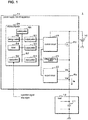
- FIG. 1 is a block diagram showing a configuration of essential parts of a power supply system 1 according to Embodiment 1.
- the power supply system 1 is favorably mounted in a vehicle, and includes a battery 10, a power supply control apparatus 11, and a capacitive load 12.
- the load 12 has a capacitor C1.
- a positive electrode of the battery 10 and one end of a capacitor C1, which is included in the load 12, are connected to the power supply control apparatus 11.
- a negative electrode of the battery 10 and the other end of the capacitor C1 included in the load 12 are grounded.
- An operation signal for giving an instruction to operate the load 12 and a stop signal for giving an instruction to stop operation of the load 12 are input to the power supply control apparatus 11.
- the power supply control apparatus 11 controls power supply from the battery 10 to the load 12 based on the input signal.
- the load 12 is an electric device that is mounted in the vehicle.
- the load 12 operates while power is supplied from the battery 10 to the load 12.
- the load 12 stops its operation while power supply from the battery 10 to the load 12 is stopped.
- the power supply control apparatus 11 has a semiconductor transistor 20, a voltage detecting portion 21, an output circuit 22, a control circuit 23, a microcomputer 24, and a resistor Ra.
- a drain is connected to the positive electrode of the battery 10, and a source is connected to one end of the resistor Ra.
- the other end of the resistor Ra is connected to one end of the capacitor C1 in the load 12.
- a gate of the semiconductor transistor 20 is connected to the control circuit 23.
- the control circuit 23 is also connected to the positive electrode of the battery 10, the output circuit 22, and the microcomputer 24.
- a voltage detecting portion 21 is connected to the source of the semiconductor transistor 20 and the microcomputer 24.
- the output circuit 22 is connected to one end and the other end of the resistor Ra, in addition to control circuit 23.
- a current is input from the positive electrode of the battery 10 to the drain of the semiconductor transistor 20, and the current input to the drain is output from the source of the semiconductor transistor 20 to the load 12 via the resistor Ra.
- the drain and the source function as an input terminal and an output terminal, respectively.
- the resistance between the drain and the source depends on the voltage at the gate (hereinafter referred to as gate voltage), which is based on a ground potential serving as a reference.
- gate voltage the voltage at the gate
- the resistance between the drain and the source decreases if the gate voltage increases.
- a voltage is applied to the gate of the semiconductor transistor 20 by the control circuit 23.
- the control circuit 23 adjusts the resistance between the drain and the source of the semiconductor transistor 20 by adjusting the gate voltage of the semiconductor transistor 20.
- the control circuit 23 functions as an adjusting portion.
- the control circuit 23 lowers the resistance between the drain and the source of the semiconductor transistor 20 by increasing the gate voltage of the semiconductor transistor 20. Thus, power is supplied from the battery 10 to the load 12 via the semiconductor transistor 20 and the resistor Ra.
- control circuit 23 increases the resistance between the drain and the source of the semiconductor transistor 20 by lowering the gate voltage of the semiconductor transistor 20. Thus, power supply from the battery 10 to the load 12 is stopped.
- control circuit 23 controls power supply to the load 12 by adjusting the resistance between the drain and the source of the semiconductor transistor 20.
- the voltage detecting portion 21 detects the voltage at the source (hereinafter referred to as source voltage) of the semiconductor transistor 20, which is based on the ground potential serving as a reference.
- the voltage detecting portion 21 outputs voltage information, which indicates the detected source voltage, to the microcomputer 24.
- the output circuit 22 outputs a voltage to the control circuit 23.
- the voltage output to the control circuit 23 by the output circuit 22 increases with an increase in a load current Ia, which is a current flowing through the load 12 via the resistor Ra, and accordingly is higher the larger the load current Ia is.
- FIG. 2 is a circuit diagram of the output circuit 22.
- the output circuit 22 has a PNP bipolar transistor 30, a differential amplifier 31, and resistors Rd and Re.
- One end of the resistor Re is connected to the source of the semiconductor transistor 20.
- the other end of the resistor Re is connected to an emitter of the bipolar transistor 30 and a minus terminal of the differential amplifier 31.
- a plus terminal of the differential amplifier 31 is connected to one end of the resistor Ra on the load 12 side.
- An output terminal of the differential amplifier 31 is connected to a base of the bipolar transistor 30.
- a collector of the bipolar transistor 30 is connected to the control circuit 23 and one end of the resistor Rd. The other end of the resistor Rd is grounded.
- the resistance between the emitter and the collector depends on the voltage at the base, which is based on the ground potential serving as a reference. If the voltage at the base of the bipolar transistor 30 increases, the resistance between the emitter and the collector of the bipolar transistor 30 increases. A voltage is applied to the base of the bipolar transistor 30 by the differential amplifier 31.
- the source voltage of the semiconductor transistor 20 will be denoted as Vs.
- the resistance between the emitter and the collector of the bipolar transistor 30 will be denoted as rb.
- the resistance values of the resistors Rd and Re will be denoted as rd and re, respectively.
- An emitter current Ie that is input to the emitter of the bipolar transistor 30 is calculated by Vs/(rb+rd+re). If the resistance value rb decreases, the emitter current Ie increases. If the resistance value rb increases, the emitter current Ie decreases.
- the voltage applied from the output terminal to the base of the bipolar transistor 30 depends on an emitter voltage Ve that is applied to the minus terminal, and on a load voltage Va that is applied to the plus terminal.
- the differential amplifier 31 lowers the voltage that is applied to the base of the bipolar transistor 30.
- the voltage decreases more the greater the difference between the emitter voltage Ve and the load voltage Va is.
- the resistance value rb between the emitter and the collector of the bipolar transistor 30 decreases due to the decrease in the voltage at the base of the bipolar transistor 30.
- the emitter current Ie increases, the magnitude of the voltage drop that occurs at the resistor Re increases, and the emitter voltage Ve decreases.
- the emitter voltage Ve comes to approximate the load voltage Va.
- the differential amplifier 31 increases the voltage applied to the base of the bipolar transistor 30.
- the voltage increases more as the difference between the emitter voltage Ve and the load voltage Va is greater.
- the resistance value rb between the emitter and the collector of the bipolar transistor 30 increases with the increase in the voltage at the base of the bipolar transistor 30.
- the emitter current Ie decreases, the magnitude of the voltage drop that occurs at the resistor Re decreases, and the emitter voltage Ve increases.
- the emitter voltage Ve comes to approximate the load voltage Va.
- ra denotes the resistance value of the resistor Ra.
- the emitter current Ie is one-thousandth of the load current Ia.
- the emitter current Ie is a fraction of a predetermined number of the load current Ia, and the predetermined number is determined by the resistance values ra and re.
- the bipolar transistor 30 and the resistors Rd and Re divide the source voltage Vs, and the divided voltage is output to the control circuit 23.
- the voltage output from the output circuit 22 to the control circuit 23 is rd ⁇ Ie. Since the emitter current Ie is expressed as Ia ⁇ ra/re as mentioned above, the voltage output from the output circuit 22 to the control circuit 23 is Ia ⁇ ra ⁇ rd/re. Since the resistance values ra, rd, and re are constants, the voltage output from the output circuit 22 to the control circuit 23 is proportional to the load current Ia.
- the emitter current Ie is largest when the resistance value rb between the emitter and the collector of the bipolar transistor 30 becomes substantially 0 ⁇ .
- the largest value of the emitter current Ie is Vs/(rd+re).
- the load current Ia that corresponds to the emitter current Ie, which is expressed as Vs/(rd+re), is Vs ⁇ re/(ra ⁇ (rd+re)).
- the equation (2) does not hold.
- the resistance value rb is substantially 0 ⁇ regardless of the load current Ia, and therefore, the voltage output from the output circuit 22 to the control circuit 23 is constant and is expressed as Vs ⁇ rd/(rd+re). Accordingly, if the source voltage Vs is low, there is a possibility that the output circuit 22 is not outputting an appropriate voltage to the control circuit 23.
- the voltage is input from the output circuit 22, and a low-level voltage or a high-level voltage is input from the microcomputer 24, to the control circuit 23 shown in FIG. 1 .
- the control circuit 23 applies a voltage to the gate of the semiconductor transistor 20.
- the control circuit 23 adjusts the gate voltage of the semiconductor transistor 20 based on the voltages input from the output circuit 22 and the microcomputer 24.
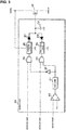
- FIG. 3 is a circuit diagram of the control circuit 23.
- the control circuit 23 has a comparator 40, a latch portion 41, an inverter 42, an AND circuit 43, an OR circuit 44, a charging circuit 45, a discharging circuit 46, a capacitor C2, and diodes D1 and D2.
- the AND circuit 43 and the OR circuit 44 each have two input terminals and one output terminal.
- the output circuit 22, or more specifically, the collector of the bipolar transistor 30 is connected to a plus terminal of the comparator 40.
- a reference voltage Vr is applied to a minus terminal of the comparator 40.
- the reference voltage Vr is constant, and is generated based on the output voltage of the battery 10 by using a regulator, for example.
- An output terminal of the comparator 40 is connected to an input terminal of the latch portion 41.
- An output terminal of the latch portion 41 is connected to an input terminal of the inverter 42 and a first input terminal of the OR circuit 44.
- An output terminal of the inverter 42 is connected to a first input terminal of the AND circuit 43. Second input terminals of the AND circuit 43 and the OR circuit 44 are separately connected to the microcomputer 24.
- the output terminal of the AND circuit 43 is connected to the charging circuit 45.
- the charging circuit 45 is also connected to the positive electrode of the battery 10 and an anode of the diode D1.
- the charging circuit 45 is grounded.
- the output terminal of the OR circuit 44 is connected to the discharging circuit 46.
- the discharging circuit 46 is also connected to a cathode of the diode D2. The discharging circuit 46 is grounded.
- a cathode of the diode D1 and an anode of the diode D2 are connected to the gate of the semiconductor transistor 20 and one end of the capacitor C2. The other end of the capacitor C2 is grounded.
- the comparator 40 If the voltage output from the output circuit 22 to the control circuit 23 is smaller than the reference voltage Vr, the comparator 40 outputs a low-level voltage to the latch portion 41. If the voltage output from the output circuit 22 to the control circuit 23 is greater than or equal to the reference voltage Vr, the comparator 40 outputs a high-level voltage to the latch portion 41.
- the latch portion 41 outputs a low-level voltage to the input terminal of the inverter 42 and the first input terminal of the OR circuit 44 while the low-level voltage is input from the comparator 40. If the voltage input from the comparator 40 switches from the low-level voltage to the high-level voltage, the latch portion 41 outputs a high-level voltage to the input terminal of the inverter 42 and the first input terminal of the OR circuit 44. After the voltage input from the comparator 40 has switched from the low-level voltage to the high-level voltage, the latch portion 41 continues to output the high-level voltage regardless of the voltage input from the comparator 40.
- the inverter 42 If the low-level voltage is input from the latch portion 41, the inverter 42 outputs a high-level voltage to the first input terminal of the AND circuit 43. If the high-level voltage is input from the latch portion 41, the inverter 42 outputs a low-level voltage to the second input terminal of the AND circuit 43. Accordingly, while the voltage output from the output circuit 22 to the control circuit 23 is smaller than the reference voltage Vr, the high-level voltage and the low-level voltage are input to the first input terminals of the AND circuit 43 and the OR circuit 44, respectively. After the voltage output from the output circuit 22 to the control circuit 23 has become larger than or equal to the reference voltage Vr, the low-level voltage and the high-level voltage continue to be input to the first input terminals of the AND circuit 43 and the OR circuit 44, respectively.
- a high-level voltage or a low-level voltage is input from the microcomputer 24 to the second input terminal of the AND circuit 43. If the high-level voltage is input to the first terminal from the inverter 42, the AND circuit 43 outputs the voltage input from the microcomputer 24 to the second input terminal, as-is, to the charging circuit 45. If the low-level voltage is input to the first terminal from the inverter 42, the AND circuit 43 outputs a low-level voltage to the charging circuit 45 regardless of the voltage input from the microcomputer 24 to the second input terminal.
- the voltage input from the microcomputer 24 to the second input terminal of the AND circuit 43 is output, as-is, to the charging circuit 45.
- the low-level voltage is output to the charging circuit 45 regardless of the voltage input from the microcomputer 24 to the second input terminal of the AND circuit 43.
- the charging circuit 45 If the high-level voltage is input from the AND circuit 43, the charging circuit 45 generates a constant voltage using the battery 10, and applies the generated voltage between both ends of the capacitor C2 via the diode D1. Thus, the capacitor C2 is charged. The voltage across both ends of the capacitor C2 is applied to the gate of the semiconductor transistor 20. As the capacitor C2 is charged, the voltage across both ends of the capacitor C2 gradually increases, and the gate voltage of the semiconductor transistor 20 gradually increases. As a result, the resistance between the drain and the source of the semiconductor transistor 20 gradually decreases.
- the charging circuit 45 stops its operation. At this time, the capacitor C2 is not charged.
- the microcomputer 24 causes the charging circuit 45 to charge the capacitor C2 by outputting the high-level voltage to the second input terminal of the AND circuit 43, and causes the charging circuit 45 to stop charging of the capacitor C2 by outputting the low-level voltage to the second input terminal of the AND circuit 43.
- a high-level voltage or a low-level voltage is input from the microcomputer 24 to the second input terminal of the OR circuit 44. If the low-level voltage is input from the latch portion 41 to the first input terminal, the OR circuit 44 outputs the voltage input from the microcomputer 24 to the second input terminal, as-is, to the discharging circuit 46. If the high-level voltage is input from the latch portion 41 to the first input terminal, the OR circuit 44 outputs a high-level voltage to the discharging circuit 46 regardless of the voltage input from the microcomputer 24 to the second input terminal.
- the voltage input from the microcomputer 24 to the second input terminal of the OR circuit 44 is output, as-is, to the discharging circuit 46.
- the high-level voltage is output to the discharging circuit 46 regardless of the voltage input from the microcomputer 24 to the second input terminal of the OR circuit 44.
- the discharging circuit 46 causes the capacitor C2 to be discharged. At this time, the cathode of the diode D2 is grounded via a resistor (not shown) in the discharging circuit 46, and a current flows from the capacitor C2 to the diode D2, the resistor in the discharging circuit 46, to the ground potential in this order. As a result of the capacitor C2 being discharged, the voltage across both ends of the capacitor C2 decreases, and the gate voltage of the semiconductor transistor 20 decreases. Thus, the resistance between the drain and the source of the semiconductor transistor 20 increases.
- the discharging circuit 46 stops its operation. At this time, the cathode of the diode D2 is open, and the capacitor C2 is not charged.
- the microcomputer 24 causes the discharging circuit 46 to discharge the capacitor C2 by outputting the high-level voltage to the second input terminal of the OR circuit 44, and causes the discharging circuit 46 to stop discharging of the capacitor C2 by outputting the low-level voltage to the second input terminal of the OR circuit 44.
- the charging circuit 45 and the discharging circuit 46 perform charging and discharging, respectively, in accordance with the voltage input from the microcomputer 24, while the voltage output from the output circuit 22 to the control circuit 23 is smaller than the reference voltage Vr. Furthermore, if the voltage output from the output circuit 22 to the control circuit 23 is larger than or equal to the reference voltage Vr, the charging circuit 45 stops its operation, and the discharging circuit 46 operates. Thus, the gate voltage of the semiconductor transistor 20 decreases, and the resistance between the drain and the source of the semiconductor transistor 20 increases. As a result, power supply from the battery 10 to the load 12 is interrupted. As a result, the voltage output from the output circuit 22 to the control circuit 23 does not exceed the reference voltage Vr.
- the reference voltage Vr corresponds to a threshold.
- the voltage output from the output circuit 22 to the control circuit 23 is expressed as Ia ⁇ ra ⁇ rd/re, where Ia denotes the load current, and ra, rd, and re denote the resistance values of the resistors Ra, Rd, and Re, respectively.
- the voltage output from the output circuit 22 to the control circuit 23 is rd ⁇ Ie, and the largest value of the emitter current Ie is Vs/(rd+re). Accordingly, the largest value of the voltage output from the output circuit 22 to the control circuit 23 is Vs ⁇ rd/(rd+re). Thus, power supply is appropriately interrupted only if this largest value Vs ⁇ rd/(rd+re) is larger than or equal to the reference voltage Vr.
- the comparator 40 continues to output the low-level voltage to the latch portion 41 regardless of the magnitude of the load current Ia.
- Vs ⁇ rd/(rd+re) of the voltage output from the output circuit 22 to the control circuit 23 increases with an increase in the source voltage Vs. Furthermore, since rd/(rd+re) ⁇ 1 holds, Vs ⁇ rd/(rd+re) ⁇ Vs holds. For this reason, the largest value Vs ⁇ rd/(rd+re) of the voltage output from the output circuit 22 to the control circuit 23 is smaller than the source voltage Vs.
- the gate voltage of the semiconductor transistor 20 is 0 V, and the drain and the source of the semiconductor transistor 20 is in an open state. At this time, no current flows through the resistor Ra, and accordingly, the source voltage Vs substantially coincides with the voltage across both ends of the capacitor C1 in the load 12, and is low. If the charging circuit 45 charges the capacitor C2 with the operation of the discharging circuit 46 stopped, the resistance between the drain and the source of the semiconductor transistor 20 gradually decreases, as mentioned above. As the resistance between the drain and the source between the semiconductor transistor 20 gradually decreases, the source voltage Vs gradually increases.
- the microcomputer 24 controls the operation of the charging circuit 45 and the discharging circuit 46 in the control circuit 23 based on the voltage information input from the voltage detecting portion 21, thereby preventing the load current Ia becoming an overcurrent while the source voltage Vs is smaller than Vr ⁇ (rd+re)/rd.
- the microcomputer 24 shown in FIG. 1 has input portions 50 and 51, output portions 52 and 53, a timer 54, a storage portion 55, and a control portion 56. These are connected to a bus 57.
- the input portion 51 is also connected to the voltage detecting portion 21.
- the output portion 52 is also connected to the second input terminal of the AND circuit 43 in the control circuit 23.
- the output portion 53 is also connected to the second input terminal of the OR circuit 44 in the control circuit 23.
- An operation signal or stop signal is input to the input portion 50. If the operation signal or stop signal is input to the input portion 50, the input portion 50 notifies the control portion 56 of this signal input.
- the voltage information is input to the input portion 51 from the voltage detecting portion 21.
- the voltage information is acquired by the control portion 56 from the input portion 51.
- the source voltage indicated by the voltage information acquired by the control portion 56 from the input portion 51 substantially coincides with the source voltage detected by the voltage detecting portion 21 when the control portion 56 acquires the voltage information.
- the output portion 52 outputs the high-level voltage or the low-level voltage to the second terminal of the AND circuit 43 in the control circuit 23.
- the output portion 52 switches the voltage output to the second terminal of the AND circuit 43 in the control circuit 23 to the high-level voltage or the low-level voltage in accordance with an instruction from the control portion 56.
- the output portion 53 outputs the high-level voltage or the low-level voltage to the second terminal of the OR circuit 44 in the control circuit 23.
- the output portion 53 switches the voltage output to the second terminal of the OR circuit 44 in the control circuit 23 to the high-level voltage or the low-level voltage in accordance with an instruction from the control portion 56.
- the timer 54 starts to measure time and ends time measurement in accordance with an instruction from the control portion 56.
- the measured time that is measured by the timer 54 is read out by the control portion 56 from the timer 54.
- the measured time that is measured by the timer 54 is reset to zero by the control portion 56.
- the storage unit 55 is a nonvolatile memory.
- a control program is stored in the storage portion 55.
- the control portion 56 includes a CPU (Central Processing Unit; not shown), and executes power supply start processing to start to supply power from the battery 10 to the load 12 and power supply end processing to end power supply from the battery 10 to the load 12, by executing the control program stored in the storage portion 55.
- CPU Central Processing Unit
- FIG. 4 is a flowchart showing a procedure of the power supply start processing executed by the control portion 56.
- the control portion 56 executes the power supply start processing if the operation signal is input to the input portion 50.
- the power supply start processing starts in a state where the output portions 52 and 53 output the low-level voltage to the second terminals of the AND circuit 43 and the OR circuit 44, respectively, in the control circuit 23, i.e. in a state where the charging circuit 45 and the discharging circuit 46 stop operation.
- step S1 the control portion 56 instructs the output portion 52 to switch the voltage output to the control circuit 23 by the output portion 52 to the high-level voltage, and thus causes the charging circuit 45 to start to charge the capacitor C2 in the control circuit 23 (step S1).
- step S1 the load current Ia is 0 A, and accordingly, the voltage output from the output circuit 22 to the control circuit 23 is smaller than the reference voltage Vr. For this reason, the voltage output to the second input terminal of the AND circuit 43 by the output portion 52 is input, as-is, from the output terminal of the AND circuit 43 to the charging circuit 45.
- control portion 56 instructs the timer 54 to start to measure time (step S2), and determines whether or not the measured time that is measured by the timer 54 is longer than or equal to charging time (step S3).
- the charging time is constant and is stored in advance in the storage portion 55. If it is determined that the measured time is shorter than the charging time (S3: NO), the control portion 56 executes step S3 again and waits until the measured time becomes longer than or equal to the charging time.
- step S4 the control portion 56 instructs the output portion 52 to switch the voltage output to the control circuit 23 by the output portion 52 to the low-level voltage, and thus causes the charging circuit 45 to end the charging of the capacitor C2 (step S4).
- the control portion 56 instructs the output portion 52 to switch the voltage output to the control circuit 23 by the output portion 52 to the low-level voltage, and thus causes the charging circuit 45 to end the charging of the capacitor C2 (step S4).
- the control portion 56 instructs the output portion 52 to switch the voltage output to the control circuit 23 by the output portion 52 to the low-level voltage, and thus causes the charging circuit 45 to end the charging of the capacitor C2 (step S4).
- the comparator 40 continues to output the low-level voltage. For this reason, in step S4, the voltage output to the second input terminal of the AND circuit 43 by the output portion 52 is input, as-is, to the charging circuit 45 in the control circuit 23.
- control portion 56 instructs the output portion 53 to switch the voltage output to the control circuit 23 by the output portion 53 to the high-level voltage, and thus causes the discharging circuit 46 to start to discharge the capacitor C2 (step S5).
- the gate voltage of the semiconductor transistor 20 decreases, and the resistance between the drain and the source of the semiconductor transistor 20 increases.
- control portion 56 resets the measured time that is measured by the timer 54 to zero (step S6), and determines whether or not the measured time that is measured by the timer 54 is longer than or equal to the discharging time (step S7).
- the discharging time is constant and is stored in advance in the storage portion 55.
- step S7 If it is determined that the measured time is shorter than the discharging time (S7: NO), the control portion 56 executes step S7 again and waits until the measured time becomes longer than or equal to the discharging time or longer. If it is determined that the measured time is longer than or equal to the discharging time (S7: YES), the control portion 56 instructs the output portion 53 to switch the voltage output to the control circuit 23 by the output portion 53 to the low-level voltage, and thus causes the discharging circuit 46 to end the discharging of the capacitor C2 (step S8). After executing step S8, the control portion 56 instructs the timer 54 to end time measurement (step S9).
- control portion 56 acquires, from the input portion 51, the voltage information input from the voltage detecting portion 21 to the input portion 51 (step S10), and determines whether or not the source voltage indicated by the acquired voltage information is larger than or equal to a standard voltage (step S11).
- the standard voltage is constant and is stored in advance in the storage portion 55.
- the source voltage being larger than or equal to the standard voltage in step S11 indicates that both ends of the capacitor C1 in the load 12 are not shorted, and the source voltage being smaller than the standard voltage indicates that both ends of the capacitor C1 in the load 12 are shorted.
- control portion 56 regards both ends of the capacitor C1 in the load 12 as being shorted and ends the power supply start processing, and does not resume charging of the capacitor C1.
- control portion 56 may also output a short circuit signal that indicates a short circuit of the capacitor C1 to an output portion (not shown), and thereafter end the power supply start processing.
- control portion 56 causes the charging circuit 45 to start to charge the capacitor C2, similarly to step S1 (step S12).
- control portion 56 After executing step S11, the control portion 56 ends the power supply start processing in a state where the charging of the capacitor C1 is continued.
- the control portion 56 performs the power supply end processing if the stop signal is input to the input portion 50.
- the control portion 56 instructs the output portions 52 and 53 to switch the voltages output by the output portions 52 and 53 to the low-level voltage and the high-level voltage, respectively.
- the charging circuit 45 ends the charging of the capacitor C1
- the discharging circuit 46 starts to discharge the capacitor C1.
- the control portion 56 instructs the output portion 53 to switch the voltage output to the control portion 56 by the output portion 53 to the low-level voltage.
- the discharging of the capacitor C1 performed by the discharging circuit 46 ends.
- the control portion 56 instructs the output portion 53 to switch the voltage output to the control portion 56 by the output portion 53 to the low-level voltage, and thereafter ends the power supply end processing.
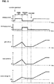
- FIG. 5 is a timing chart showing an example of operations in the power supply control apparatus 11.
- FIG. 5 shows graphs of the voltages input to the charging circuit 45 and the discharging circuit 46, and graphs of the gate voltage, load current Ia, and the source voltage Vs. These graphs occur in the case where both ends of the load 12 are not shorted.
- the horizontal axis indicates time.
- a high-level voltage is denoted as "H”
- a low-level voltage is denoted as "L”.
- the control portion 56 in the microcomputer 24 executes the power supply start processing if the operation signal is input to the input portion 50 in the microcomputer 24.
- the microcomputer 24 switches the voltage input to the charging circuit 45 to the high-level voltage while keeping the voltage input to the discharging circuit 46 to the low-level voltage, and causes the charging circuit 45 in the control circuit 23 to start to charge the capacitor C2.
- the voltage across both ends of the capacitor C2, i.e. the gate voltage gradually increases, and the resistance between the drain and the source of the semiconductor transistor 20 gradually decreases.
- the load current Ia flows from the battery 10 to the load 12 via the semiconductor transistor 20. As the resistance between the drain and the source of the semiconductor transistor 20 gradually decreases, the load current Ia also gradually increases.
- the source voltage Vs of the semiconductor transistor 20 gradually increases as the resistance between the drain and the source of the semiconductor transistor 20 gradually decreases. Also, as a result of power being supplied from the battery 10 to the load 12, the capacitor C1 in the load 12 is charged, and the voltage across both ends of the capacitor C1 also increases.
- the microcomputer 24 switches the voltage input to the charging circuit 45 to the low-level voltage, and causes the charging circuit 45 to end the charging of the capacitor C2.
- the increase in the gate voltage, the load current Ia, the source voltage, and the voltage across both ends of the capacitor C1 stop.
- the microcomputer 24 switches the voltage input to the discharging circuit 46 from the low-level voltage to the high-level voltage, and causes the discharging circuit 46 to start to discharge the capacitor C2.
- the voltage across both ends of the capacitor C2 decreases, and the gate voltage of the semiconductor transistor 20 decreases.
- the resistance between the drain and the source of the semiconductor transistor 20 increases, and the load current Ia decreases.
- the source voltage Vs also decreases to the voltage across both ends of the capacitor C1.
- the discharging time is sufficiently longer than the time required for the voltage across both ends of the capacitor C2 to become 0 V due to the discharging performed by the discharging circuit 46. For this reason, when the discharging time has elapsed since the voltage input to the discharging circuit 46 was switched from the low-level voltage to the high-level voltage, the gate voltage is 0 V, and the drain and the source of the semiconductor transistor 20 are in an open state. When the discharging time has elapsed, no current is flowing through the resistor Ra, and accordingly, the source voltage Vs coincides with the voltage across both ends of the capacitor C1.
- the voltage across both ends of the capacitor C1 becomes larger than or equal to a standard voltage Vb until the charging time has elapsed since the operation signal was input to the input portion 50. Accordingly, unless both ends of the load 12 are shorted, the source voltage Vs is larger than or equal to the standard voltage Vb when the discharging time has elapsed.
- the control portion 56 in the microcomputer 24 determines whether or not the source voltage Vs indicated by the voltage information input from the voltage detecting portion 21 is larger than or equal to the standard voltage Vb. If it is determined by the control portion 56 that the source voltage Vs is larger than or equal to the standard voltage Vb, the microcomputer 24 regards both ends of the load 12 as not being shorted, and switches the voltage input to the charging circuit 45 from the low-level voltage to the high-level voltage, and the control portion 56 in the microcomputer 24 ends the power supply start processing.
- the control portion 56 functions as a determining portion, and the standard voltage Vb corresponds to a predetermined voltage.
- the charging circuit 45 again charges the capacitor C2 in the control circuit 23, increases the gate voltage of the semiconductor transistor 20, and decreases the resistance between the drain and the source of the semiconductor transistor 20. As a result, power is supplied from the battery 10 to the load 12, and the load current Ia and the source voltage Vs increase again.
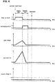
- FIG. 6 is a timing chart showing another example of operations of the power supply control apparatus 11. Similar to FIG. 5 , FIG. 6 shows graphs of the voltages input to the charging circuit 45 and the discharging circuit 46, and graphs of the gate voltage, the load current Ia, and the source voltage Vs. These graphs are for the case where both ends of the load 12 are shorted. The horizontal axis indicates time. In FIG. 6 as well, a high-level voltage is denoted as "H”, and a low-level voltage is denoted as "L".
- control portion 56 in the microcomputer 24 executes the power supply start processing if the operation signal is input to the input portion 50 in the microcomputer 24.
- the microcomputer 24 switches the voltage input to the charging circuit 45 in the control circuit 23 to the high-level voltage while keeping the voltage input to the discharging circuit 46 to the low-level voltage, and causes the charging circuit 45 to start to charge the capacitor C2.
- the voltage across both ends of the capacitor C2 gradually increases, and the resistance between the drain and the source of the semiconductor transistor 20 gradually decreases.
- the load current Ia that flows through the resistor Ra sharply increases as the resistance between the drain and the source of the semiconductor transistor 20 decreases. Also, since both ends of the load 12 are shorted, the source voltage Vs is substantially 0 V.
- the microcomputer 24 switches the voltage input to the charging circuit 45 to the low-level voltage, and causes the charging circuit 45 to end the charging of the capacitor C2.
- the gate voltage and the load current Ia stop increasing.
- the microcomputer 24 switches the voltage input to the discharging circuit 46 from the low-level voltage to the high-level voltage, and causes the discharging circuit 46 to start to discharge the capacitor C2.
- the voltage across both ends of the capacitor C2 decreases, and the gate voltage of the semiconductor transistor 20 decreases.
- the resistance between the drain and the source of the semiconductor transistor 20 increases, and the load current Ia decreases.
- the microcomputer 24 restores the voltage input to the discharging circuit 46 to the low-level voltage, and the discharging circuit 46 ends the discharging of the capacitor C2.
- the gate voltage is 0 V
- the drain and the source of the semiconductor transistor 20 are in an open state.
- the source voltage Vs is substantially 0 V, and is smaller than the standard voltage Vb.
- the control portion 56 in the microcomputer 24 determines whether or not the source voltage Vs indicated by the voltage information input from the voltage detecting portion 21 is larger than or equal to the standard voltage Vb. If it is determined by the control portion 56 that the source voltage Vs is smaller than the standard voltage Vb, the power supply start processing ends while the voltages input to the charging circuit 45 and the discharging circuit 46 are kept to the low-level voltage.
- the control portion 56 keeps the resistance between the drain and the source of the semiconductor transistor 20 to the resistance at the time when the determination was performed, and reliably prevents an overcurrent from flowing through the semiconductor transistor 20.
- the discharging circuit 46 discharges the capacitor C1 to temporarily stop power supply from the battery 10 to the load 12. Accordingly, power is not needlessly consumed when both ends of the load 12 are shorted.
- the source voltage Vs is larger than or equal to Vr ⁇ (rd+re)/rd
- the largest value of the voltage output from the output circuit 22 to the control circuit 23 is larger than or equal to the reference voltage Vr. For this reason, an overcurrent is prevented from flowing through the semiconductor transistor 20 by adjusting the resistance between the drain and the source of the semiconductor transistor 20 based on the voltage output from the output circuit 22 to the control circuit 23.
- the source voltage Vs is smaller than Vr ⁇ (rd+re)/rd
- the largest value of the voltage output from the output circuit 22 to the control circuit 23 is smaller than the reference voltage Vr. For this reason, a flow of an overcurrent is prevented by adjusting the resistance between the drain and the source of the semiconductor transistor 20 based on the source voltage Vs indicated by the voltage information input from the voltage detecting portion 21.
- the power supply system 1 is configured similarly to Embodiment 1, whereas the content of the power supply start processing executed by the control portion 56 in the microcomputer 24 differs from Embodiment 1.
- Embodiment 2 the content of the power supply start processing executed by the control portion 56 according to Embodiment 2 will be described.
- the structures that are common to Embodiment 1 are assigned the same reference signs as those in Embodiment 1, and a description thereof will be omitted accordingly.
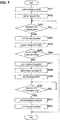
- FIG. 7 is a flowchart showing a procedure of the power supply start processing executed by a control portion 56 according to Embodiment 2.
- the control portion 56 executes the power supply start processing if the operation signal is input to the input portion 50.
- the power supply start processing starts in a state where the output portions 52 and 53 output the low-level voltage to the second terminals of the AND circuit 43 and the OR circuit 44, respectively, in the control circuit 23, i.e. in a state where the charging circuit 45 and the discharging circuit 46 stop operation.
- the control portion 56 causes the charging circuit 45 to start to charge the capacitor C2 in the control circuit 23 (step S21), and instructs the timer 54 to start to measure time (step S22).
- the control portion 56 determines whether or not the measured time that is measured by the timer 54 is longer than or equal to the charging time (step S23). If it is determined that the measured time is shorter than the charging time (S23: NO), the control portion 56 again executes step S23 and waits until the measured time becomes longer than or equal to the charging time.
- the control portion 56 instructs the timer 54 to end time measurement (step S24), and acquires, from the input portion 51, the voltage information input from the voltage detecting portion 21 to the input portion 51 (step S25). At this point, the charging of the capacitor C2 in the control circuit 23 is continued.
- control portion 56 determines whether or not the source voltage indicated by the voltage information acquired in step S25 is larger than or equal to the standard voltage (step S26). Unless both ends of the capacitor C2 in the load 12 are shorted, the voltage across both ends of the capacitor C1 is larger than or equal to the standard voltage, similarly to Embodiment 2. If both ends of the capacitor C2 in the load 12 are shorted, hardly any power is stored in the capacitor C1, and the voltage across both ends of the capacitor C1 is substantially 0 V and is smaller than the standard voltage.
- control portion 56 causes the charging circuit 45 to end the charging of the capacitor C2 (step S27), similarly to step S4 in the power supply start processing according to Embodiment 1. After executing step S27, the control portion 56 causes the discharging circuit 46 to start to discharge the capacitor C2 (step S28), similarly to step S5 in the power supply start processing according to Embodiment 1.
- control portion 56 instructs the timer 54 to measure time (step S29), and determines whether or not the measured time that is measured by the timer 54 is longer than or equal to the discharging time (step S30). If it is determined that the measured time is shorter than the discharging time (S30: NO), the control portion 56 again executes step S30 and waits until the measured time becomes longer than or equal to the discharging time.
- the control portion 56 causes the discharging circuit 46 to end the discharging of the capacitor C2 (step S31) similarly to step S8 in the power supply start processing according to Embodiment 1, and instructs the timer 54 to end time measurement (step S32). If it is determined that the source voltage is larger than or equal to the standard voltage (S26: YES), or after the control portion 56 has executed step S32, the control portion 56 ends the power supply start processing.
- control portion 56 executes step S32 and ends the power supply start processing, the control portion 56 does not resume the charging of the capacitor C1 since both ends of the capacitor C1 in the load 12 are shorted.
- control portion 56 determines that the source voltage is larger than or equal to the standard voltage and ends the power supply start processing, the control portion 56 ends the power supply start processing in a state where the charging circuit 45 continues to charge the capacitor C1, since both ends of the capacitor C1 in the load 12 are not shorted.
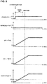
- FIG. 8 is a timing chart showing an example of operations of the power supply control apparatus 11. Similar to FIG. 5 , FIG. 8 shows graphs of the voltages input to the charging circuit 45 and the discharging circuit 46, and graphs of the gate voltage, the load current Ia, and the source voltage Vs. These graphs occur in the case where both ends of the load 12 are not shorted. The horizontal axis indicates time. In FIG. 8 as well, a high-level voltage is denoted as "H”, and a low-level voltage is denoted as "L".
- control portion 56 in the microcomputer 24 executes the power supply start processing if the operation signal is input to the input portion 50 in the microcomputer 24.
- the microcomputer 24 switches the voltage input to the charging circuit 45 to the high-level voltage while keeping the voltage input to the discharging circuit 46 to the low-level voltage, and the charging circuit 45 in the control circuit 23 starts to charge the capacitor C2, similarly to Embodiment 1.
- the gate voltage of the semiconductor transistor 20 gradually increases, and the resistance between the drain and the source of the semiconductor transistor 20 gradually decreases. With this decrease in the resistance, the load current Ia also gradually increases. Unless both ends of the load 12 are shorted, the source voltage Vs of the semiconductor transistor 20 also gradually increases. Also, as a result of the load current Ia flowing from the battery 10 to the load 12, the capacitor C1 in the load 12 is charged, and the voltage across both ends of the capacitor C1 also increases.
- the control portion 56 in the microcomputer 24 determines whether or not the source voltage Vs indicated by the voltage information input from the voltage detecting portion 21 is larger than or equal to the standard voltage Vb. At this time, the high-level voltage is input to the charging circuit 45, and the charging circuit 45 continues to charge the capacitor C2.
- the microcomputer 24 regards both ends of the load 12 as not being shorted, keeps the voltage input to the charging circuit 45 to the high-level voltage, and continues to lower the resistance between the drain and the source of the semiconductor transistor 20.
- the control portion 56 ends the power supply start processing while keeping the voltage input to the charging circuit 45 to the high-level voltage.
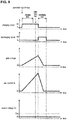
- FIG. 9 is a timing chart showing another example of operations of the power supply control apparatus 11. Similar to FIG. 8 , FIG. 9 shows graphs of the voltages input to the charging circuit 45 and the discharging circuit 46, and graphs of the gate voltage, the load current Ia, and the source voltage Vs. These graphs are for the case where both ends of the load 12 are shorted. The horizontal axis indicates time. In FIG. 9 as well, a high-level voltage is denoted as "H”, and a low-level voltage is denoted as "L".
- control portion 56 in the microcomputer 24 executes the power supply start processing if the operation signal is input to the input portion 50 in the microcomputer 24. Initially, the microcomputer 24 switches the voltage input to the charging circuit 45 in the control circuit 23 to the high-level voltage while keeping the voltage input to the discharging circuit 46 to the low-level voltage, and the charging circuit 45 starts to charge the capacitor C2, similarly to Embodiment 1.
- the gate voltage of the semiconductor transistor 20 gradually increases, and the resistance between the drain and the source of the semiconductor transistor 20 gradually decreases.
- a current flows from the battery 10 to the load 12 via the semiconductor transistor 20.
- the load current Ia that flows through the resistor Ra sharply increases as the resistance between the drain and the source of the semiconductor transistor 20 decreases.
- the source voltage Vs is substantially 0 V.
- the control portion 56 in the microcomputer 24 determines whether or not the source voltage Vs indicated by the voltage information input from the voltage detecting portion 21 is larger than or equal to the standard voltage Vb. At this time, the high-level voltage is input to the charging circuit 45, and the charging circuit 45 continues to charge the capacitor C2.
- the microcomputer 24 regards both ends of the load 12 as being shorted, and switches the voltages input to the charging circuit 45 and the discharging circuit 46 to the low-level voltage and the high-level voltage, respectively.
- the charging circuit 45 ends the charging of the capacitor C2
- the discharging circuit 46 starts to discharge the capacitor C2.
- the voltage across both ends of the capacitor C2 decreases, and the gate voltage of the semiconductor transistor 20 decreases.
- the resistance between the drain and the source of the semiconductor transistor 20 increases, and the load current Ia decreases.
- the source voltage Vs remains substantially 0 V.
- the microcomputer 24 restores the voltage input to the discharging circuit 46 from the high-level voltage to the low-level voltage, and the discharging circuit 46 ends the discharging of the capacitor C2.
- the control portion 56 increases the resistance between the drain and the source of the semiconductor transistor 20 to a resistance higher than the resistance at the time when the determination was performed, and reliably prevents an overcurrent from flowing through the semiconductor transistor 20.
- the source voltage Vs is larger than or equal to Vr ⁇ (rd+re)/rd
- an overcurrent is prevented from flowing through the semiconductor transistor 20 by adjusting the resistance between the drain and the source of the semiconductor transistor 20 based on the voltage output from the output circuit 22 to the control circuit 23, similarly to Embodiment 1.
- the source voltage Vs is smaller than Vr ⁇ (rd+re)/rd
- a flow of an overcurrent is prevented by adjusting the resistance between the drain and the source of the semiconductor transistor 20 based on the source voltage Vs indicated by the voltage information input from the voltage detecting portion 21.
- the capacitor C2 in the control circuit 23 need only be a capacitor whose one end is connected to the gate of the semiconductor transistor 20. Accordingly, the other end of the capacitor C2 may also be connected to the drain or the source of the semiconductor transistor 20. In this case, the capacitor C2 may also be an input capacitance that is formed when the semiconductor transistor 20 is manufactured.
- the semiconductor transistor 20 is not limited to an N-channel FET, and may also be an NPN bipolar transistor, for example. Furthermore, the semiconductor transistor 20 may also be a P-channel FET, a PNP bipolar transistor, or the like. For example, if the semiconductor transistor 20 is a P-channel FET, the drain is connected to one end of the capacitor C1 in the load 12, and the source is connected to the positive electrode of the battery 10.
- the control circuit 23 gradually increases the resistance between the source and the drain of the semiconductor transistor 20 by gradually lowering the voltage at the gate, and gradually lowers the resistance between the source and the drain of the semiconductor transistor 20 by gradually increasing the voltage at the gate.
- the output circuit 22 is not limited to a circuit that is constituted by the PNP bipolar transistor 30, the differential amplifier 31, and the resistors Rd and Re.
- the output circuit 22 need only be a circuit that outputs a voltage that is proportional to the load current Ia and whose largest value is smaller than or equal to the source voltage Vs.
- Embodiments 1 and 2 disclosed above are examples in all aspects, and should be considered to be non-restrictive.
- the scope of the present invention is indicated not by the above-stated meanings but by the claims, and is intended to include all modifications within the meanings and scope equivalent to the claims.
Landscapes
- Engineering & Computer Science (AREA)
- Power Engineering (AREA)
- Physics & Mathematics (AREA)
- Electromagnetism (AREA)
- General Physics & Mathematics (AREA)
- Radar, Positioning & Navigation (AREA)
- Automation & Control Theory (AREA)
- Direct Current Feeding And Distribution (AREA)
- Charge And Discharge Circuits For Batteries Or The Like (AREA)
- Emergency Protection Circuit Devices (AREA)
Abstract
Description
- The present invention relates to a power supply control apparatus for controlling power supply from a battery to a load.
- Vehicles are equipped with a power supply control apparatus for controlling power supply to a capacitive load by turning ON or OFF a switch that is provided on a current path from a battery to the load. In this power supply control apparatus, if the switch is turned ON from the OFF state with a small amount of power being stored in a capacitor that is included in the load, a large current temporarily flows from the battery to the load since there is a large voltage difference between the battery and the load, and the resistance between both ends of the switch is small. This current is called "inrush current". If an inrush current flows, for example, there is a concern that constituent components of the load will be burn out.
-
Patent Document 1 discloses a power supply control apparatus that prevents the occurrence of an inrush current. In this power supply control apparatus, one end of a series circuit of a resistor and a second switch is connected to one end of a switch, the other end of this series circuit is connected to the other end of the switch, and a current flows from a battery to a load via the switch or the series circuit. The second switch is turned ON from the OFF state before turning ON the switch from the OFF state. Thus, a current flows from the battery to the load via the resistor and the second switch. - Here, since a current flows through the load via the resistor, an inrush current does not flow even if the amount of power stored in a capacitor in the load is small. After a certain amount of power is stored in the capacitor, the second switch is turned OFF, and the switch is turned ON. Thus, power can be supplied from the battery to the load via the switch, while no power is consumed by the resistor in the series circuit.
- Patent Document 1:
JP 2004-135389A - A power supply control apparatus that includes a semiconductor transistor, e.g. an FET (Field Effect Transistor) is conceivable as a power supply control apparatus that prevents an inrush current from flowing through a load, such as the power supply control apparatus described in
Patent Document 1. In this power supply control apparatus, a semiconductor transistor is connected between a positive electrode of a battery and one end of a load, and a negative electrode of the battery and the other end of the load are grounded. In the semiconductor transistor, a current is input from the battery to an input terminal, and the input current is output from an output terminal to the load. A resistance between the input terminal and the output terminal of the semiconductor transistor is adjusted by adjusting a voltage at a control end of the semiconductor transistor, e.g. a gate of an FET. In this power supply control apparatus, the resistance between the input terminal and the output terminal of the semiconductor transistor is gradually lowered. Thus, an inrush current is prevented from flowing through the load. - Usually, a power supply control apparatus for controlling power supply to a load via a semiconductor transistor is provided with a configuration in which an overcurrent is prevented from flowing through the semiconductor transistor. For example, an output circuit is provided that outputs a higher voltage as the current flowing through the load is larger. If the voltage output by the output circuit is larger than or equal to a predetermined voltage, the resistance between the input terminal and the output terminal of the semiconductor transistor is increased. Thus, a current that is larger than or equal to a predetermined current does not flow through the semiconductor transistor, and an overcurrent is prevented from flowing through the semiconductor transistor.
- However, if the output circuit is configured to generate the voltage to be output by dividing the voltage at the output terminal of the semiconductor transistor, the output circuit cannot output a voltage that exceeds the predetermined voltage when the voltage at the output terminal of the semiconductor transistor is smaller than the predetermined voltage.
- Accordingly, when the resistance between the input terminal and the output terminal of the semiconductor transistor is lowered to supply power to the load, even if a current that is larger than or equal to the predetermined current flows while the voltage at the output terminal of the semiconductor transistor is smaller than the predetermined voltage, the resistance between the input terminal and the output terminal of the semiconductor transistor is not increased. The power supply control apparatus that includes such an output circuit has a problem in that a flow of an overcurrent cannot be reliably prevented.
- The present invention has been made in view of the foregoing situation, and aims to provide a power supply control apparatus capable of reliably preventing a flow of an inrush current and an overcurrent.
- A power supply control apparatus according to the present invention is A power supply control apparatus that includes a semiconductor transistor for outputting a current that is input to its input terminal, from its output terminal to a capacitive load, and an adjusting portion for adjusting a resistance between the input terminal and the output terminal of the semiconductor transistor, and controls power supply to the load by adjusting the resistance with the adjusting portion, the power supply control apparatus including: a detecting portion for detecting a voltage at the output terminal; and a determining portion for determining whether or not the voltage at the output terminal detected by the detecting portion is larger than or equal to a predetermined voltage, after the adjusting portion has lowered the resistance, wherein the adjusting portion again lowers the resistance if it is determined by the determining portion that the voltage at the output terminal is larger than or equal to the predetermined voltage, and if it is determined by the determining portion that the voltage at the output terminal is smaller than the predetermined voltage, adjusts the resistance to at least the resistance at the time when the determining portion performed the determination.
- In the present invention, for example, a current is input to the input terminal of the semiconductor transistor from the battery, and the input current is output from the output terminal of the semiconductor transistor to the capacitive load. By gradually increasing the resistance between the input terminal and the output terminal of the semiconductor transistor, an inrush current can be reliably prevented from flowing through the semiconductor transistor.
- The resistance between the input terminal and the output terminal of the semiconductor transistor is lowered to supply power to the load. Thus, power is stored in the capacitor in the load. After the resistance is lowered, it is determined whether or not the detected voltage at the output terminal is larger than or equal to the predetermined voltage. If both ends of the load are shorted and there is a possibility that an overcurrent will flow through the semiconductor transistor, the voltage at the output terminal is substantially 0 V, and accordingly is smaller than the predetermined voltage. If both ends of the load are not shorted, the voltage at the output terminal is larger than or equal to the predetermined voltage.
- If it is determined that the voltage at the output terminal is larger than or equal to the predetermined voltage, the resistance between the input terminal and the output terminal of the semiconductor transistor is lowered again, and power is supplied to the load. If it is determined that the voltage at the output terminal is smaller than the predetermined voltage, the resistance between the input terminal and the output terminal of the semiconductor transistor is adjusted to a resistance at the time when the determination was performed or larger, and an overcurrent is reliably prevented from flowing through the semiconductor transistor.
- In the power supply control apparatus according to the present invention, the adjusting portion lowers the resistance and thereafter increases the resistance before the determining portion performs the determination, and the determining portion performs the determination after the adjusting portion has increased the resistance.
- In the present invention, the resistance between the input terminal and the output terminal of the semiconductor transistor is lowered, and power is supplied to the capacitor in the load. Then, the resistance is increased, and power supply is stopped. Thereafter, it is determined whether or not the voltage at the output terminal of the semiconductor transistor is larger than or equal to the predetermined voltage. Since power supply temporarily stops, power is not needlessly consumed when both ends of the load are shorted.
- The power supply control apparatus according to the present invention further includes an output circuit that outputs a higher voltage the larger a current flowing through the load is, wherein the adjusting portion increases the resistance if the voltage output by the output circuit is larger than or equal to a threshold, and the largest value of the voltage output by the output circuit is smaller than or equal to the voltage at the output terminal, and increases with an increase in the voltage at the output terminal.
- In the present invention, if the voltage output by the output circuit is larger than or equal to the threshold, the resistance between the input terminal and the output terminal of the semiconductor transistor is increased. If the voltage at the output terminal of the semiconductor transistor is high, the largest value of the voltage output by the output circuit is large. For this reason, a configuration in which the resistance is increased based on the voltage output by the output circuit appropriately works. Accordingly, a flow of an overcurrent is prevented. If the voltage at the output terminal of the semiconductor transistor is low, the smallest value of the voltage output by the output circuit is small. For this reason, the configuration in which the resistance is increased based on the voltage output by the output circuit does not appropriately work. A flow of an overcurrent is prevented by resistance adjustment that is performed based on the detected voltage at the output terminal.
- According to the present invention, a flow of an inrush current and an overcurrent can be reliably prevented.
-
-
FIG. 1 is a block diagram showing a configuration of essential parts of a power supply system according toEmbodiment 1. -
FIG. 2 is a circuit diagram of an output circuit. -
FIG. 3 is a circuit diagram of a control circuit. -
FIG. 4 is a flowchart showing a procedure of start processing executed by a control portion. -
FIG. 5 is a timing chart showing an example of operations in a power supply control apparatus. -
FIG. 6 is a timing chart showing another example of operations in the power supply control apparatus. -
FIG. 7 is a flowchart showing a procedure of start processing executed by a control portion according to Embodiment 2. -
FIG. 8 is a timing chart showing an example of operations of the power supply control apparatus. -
FIG. 9 is a timing chart showing another example of operations of the power supply control apparatus. - Hereinafter, the present invention will be described in detail based on the drawings illustrating the embodiments.
-
FIG. 1 is a block diagram showing a configuration of essential parts of apower supply system 1 according toEmbodiment 1. Thepower supply system 1 is favorably mounted in a vehicle, and includes abattery 10, a powersupply control apparatus 11, and acapacitive load 12. Theload 12 has a capacitor C1. A positive electrode of thebattery 10 and one end of a capacitor C1, which is included in theload 12, are connected to the powersupply control apparatus 11. A negative electrode of thebattery 10 and the other end of the capacitor C1 included in theload 12 are grounded. - An operation signal for giving an instruction to operate the
load 12 and a stop signal for giving an instruction to stop operation of theload 12 are input to the powersupply control apparatus 11. The powersupply control apparatus 11 controls power supply from thebattery 10 to theload 12 based on the input signal. - The
load 12 is an electric device that is mounted in the vehicle. Theload 12 operates while power is supplied from thebattery 10 to theload 12. Theload 12 stops its operation while power supply from thebattery 10 to theload 12 is stopped. - The power
supply control apparatus 11 has asemiconductor transistor 20, avoltage detecting portion 21, anoutput circuit 22, acontrol circuit 23, amicrocomputer 24, and a resistor Ra. Of thesemiconductor transistor 20, a drain is connected to the positive electrode of thebattery 10, and a source is connected to one end of the resistor Ra. The other end of the resistor Ra is connected to one end of the capacitor C1 in theload 12. A gate of thesemiconductor transistor 20 is connected to thecontrol circuit 23. Thecontrol circuit 23 is also connected to the positive electrode of thebattery 10, theoutput circuit 22, and themicrocomputer 24. Avoltage detecting portion 21 is connected to the source of thesemiconductor transistor 20 and themicrocomputer 24. Theoutput circuit 22 is connected to one end and the other end of the resistor Ra, in addition tocontrol circuit 23. - A current is input from the positive electrode of the
battery 10 to the drain of thesemiconductor transistor 20, and the current input to the drain is output from the source of thesemiconductor transistor 20 to theload 12 via the resistor Ra. The drain and the source function as an input terminal and an output terminal, respectively. - In the
semiconductor transistor 20, the resistance between the drain and the source depends on the voltage at the gate (hereinafter referred to as gate voltage), which is based on a ground potential serving as a reference. In thesemiconductor transistor 20, the resistance between the drain and the source decreases if the gate voltage increases. A voltage is applied to the gate of thesemiconductor transistor 20 by thecontrol circuit 23. Thecontrol circuit 23 adjusts the resistance between the drain and the source of thesemiconductor transistor 20 by adjusting the gate voltage of thesemiconductor transistor 20. Thecontrol circuit 23 functions as an adjusting portion. - The
control circuit 23 lowers the resistance between the drain and the source of thesemiconductor transistor 20 by increasing the gate voltage of thesemiconductor transistor 20. Thus, power is supplied from thebattery 10 to theload 12 via thesemiconductor transistor 20 and the resistor Ra. - Also, the
control circuit 23 increases the resistance between the drain and the source of thesemiconductor transistor 20 by lowering the gate voltage of thesemiconductor transistor 20. Thus, power supply from thebattery 10 to theload 12 is stopped. - As described above, the
control circuit 23 controls power supply to theload 12 by adjusting the resistance between the drain and the source of thesemiconductor transistor 20. - The
voltage detecting portion 21 detects the voltage at the source (hereinafter referred to as source voltage) of thesemiconductor transistor 20, which is based on the ground potential serving as a reference. Thevoltage detecting portion 21 outputs voltage information, which indicates the detected source voltage, to themicrocomputer 24. - The
output circuit 22 outputs a voltage to thecontrol circuit 23. The voltage output to thecontrol circuit 23 by theoutput circuit 22 increases with an increase in a load current Ia, which is a current flowing through theload 12 via the resistor Ra, and accordingly is higher the larger the load current Ia is. -
FIG. 2 is a circuit diagram of theoutput circuit 22. Theoutput circuit 22 has a PNPbipolar transistor 30, adifferential amplifier 31, and resistors Rd and Re. One end of the resistor Re is connected to the source of thesemiconductor transistor 20. The other end of the resistor Re is connected to an emitter of thebipolar transistor 30 and a minus terminal of thedifferential amplifier 31. A plus terminal of thedifferential amplifier 31 is connected to one end of the resistor Ra on theload 12 side. An output terminal of thedifferential amplifier 31 is connected to a base of thebipolar transistor 30. A collector of thebipolar transistor 30 is connected to thecontrol circuit 23 and one end of the resistor Rd. The other end of the resistor Rd is grounded. - Most of the current output from the source of the
semiconductor transistor 20 flows through theload 12 via the resistor Ra. The remainder of the current output from the source of thesemiconductor transistor 20 flows to the resistor Re, thebipolar transistor 30, and the resistor Rd in this order. In thebipolar transistor 30, the current is input to the emitter, and the current input to the emitter is output from the collector to the resistor Rd. - In the
bipolar transistor 30, the resistance between the emitter and the collector depends on the voltage at the base, which is based on the ground potential serving as a reference. If the voltage at the base of thebipolar transistor 30 increases, the resistance between the emitter and the collector of thebipolar transistor 30 increases. A voltage is applied to the base of thebipolar transistor 30 by thedifferential amplifier 31. - The source voltage of the
semiconductor transistor 20 will be denoted as Vs. The resistance between the emitter and the collector of thebipolar transistor 30 will be denoted as rb. The resistance values of the resistors Rd and Re will be denoted as rd and re, respectively. An emitter current Ie that is input to the emitter of thebipolar transistor 30 is calculated by Vs/(rb+rd+re). If the resistance value rb decreases, the emitter current Ie increases. If the resistance value rb increases, the emitter current Ie decreases. - In the
differential amplifier 31, the voltage applied from the output terminal to the base of thebipolar transistor 30 depends on an emitter voltage Ve that is applied to the minus terminal, and on a load voltage Va that is applied to the plus terminal. - If the emitter voltage Ve is higher than the load voltage Va, the
differential amplifier 31 lowers the voltage that is applied to the base of thebipolar transistor 30. The voltage decreases more the greater the difference between the emitter voltage Ve and the load voltage Va is. The resistance value rb between the emitter and the collector of thebipolar transistor 30 decreases due to the decrease in the voltage at the base of thebipolar transistor 30. As a result, the emitter current Ie increases, the magnitude of the voltage drop that occurs at the resistor Re increases, and the emitter voltage Ve decreases. The emitter voltage Ve comes to approximate the load voltage Va. - If the emitter voltage Ve is lower than the load voltage Va, the
differential amplifier 31 increases the voltage applied to the base of thebipolar transistor 30. The voltage increases more as the difference between the emitter voltage Ve and the load voltage Va is greater. The resistance value rb between the emitter and the collector of thebipolar transistor 30 increases with the increase in the voltage at the base of thebipolar transistor 30. As a result, the emitter current Ie decreases, the magnitude of the voltage drop that occurs at the resistor Re decreases, and the emitter voltage Ve increases. The emitter voltage Ve comes to approximate the load voltage Va. - As described above, the
differential amplifier 31 adjusts the resistance value rb between the emitter and the collector of thesemiconductor transistor 20 so that the emitter voltage Ve coincides with the load voltage Va. Since the emitter voltage Ve coincides with the load voltage Va, the following equation (1) holds.
- Here, ra denotes the resistance value of the resistor Ra.
- The following equation (2) holds as a result of expanding the equation (1).

- For example, if the resistance value re is 1000 times the resistance value ra, the emitter current Ie is one-thousandth of the load current Ia. Thus, the emitter current Ie is a fraction of a predetermined number of the load current Ia, and the predetermined number is determined by the resistance values ra and re.
- The
bipolar transistor 30 and the resistors Rd and Re divide the source voltage Vs, and the divided voltage is output to thecontrol circuit 23. The voltage output from theoutput circuit 22 to thecontrol circuit 23 is rd×Ie. Since the emitter current Ie is expressed as Ia×ra/re as mentioned above, the voltage output from theoutput circuit 22 to thecontrol circuit 23 is Ia×ra×rd/re. Since the resistance values ra, rd, and re are constants, the voltage output from theoutput circuit 22 to thecontrol circuit 23 is proportional to the load current Ia. - However, the range of the load current Ia in which the voltage output from the
output circuit 22 to thecontrol circuit 23 is proportional to the load current Ia is limited. - The emitter current Ie is largest when the resistance value rb between the emitter and the collector of the
bipolar transistor 30 becomes substantially 0 Ω. The largest value of the emitter current Ie is Vs/(rd+re). The load current Ia that corresponds to the emitter current Ie, which is expressed as Vs/(rd+re), is Vs×re/(ra×(rd+re)). - Accordingly, if the load current Ia exceeds Vs×re/(ra×(rd+re)), the equation (2) does not hold. In this case, the resistance value rb is substantially 0 Ω regardless of the load current Ia, and therefore, the voltage output from the
output circuit 22 to thecontrol circuit 23 is constant and is expressed as Vs×rd/(rd+re). Accordingly, if the source voltage Vs is low, there is a possibility that theoutput circuit 22 is not outputting an appropriate voltage to thecontrol circuit 23. - The voltage is input from the
output circuit 22, and a low-level voltage or a high-level voltage is input from themicrocomputer 24, to thecontrol circuit 23 shown inFIG. 1 . Thecontrol circuit 23 applies a voltage to the gate of thesemiconductor transistor 20. Thecontrol circuit 23 adjusts the gate voltage of thesemiconductor transistor 20 based on the voltages input from theoutput circuit 22 and themicrocomputer 24. -
FIG. 3 is a circuit diagram of thecontrol circuit 23. Thecontrol circuit 23 has acomparator 40, alatch portion 41, aninverter 42, an ANDcircuit 43, an ORcircuit 44, a chargingcircuit 45, a dischargingcircuit 46, a capacitor C2, and diodes D1 and D2. The ANDcircuit 43 and theOR circuit 44 each have two input terminals and one output terminal. - The
output circuit 22, or more specifically, the collector of thebipolar transistor 30 is connected to a plus terminal of thecomparator 40. A reference voltage Vr is applied to a minus terminal of thecomparator 40. The reference voltage Vr is constant, and is generated based on the output voltage of thebattery 10 by using a regulator, for example. An output terminal of thecomparator 40 is connected to an input terminal of thelatch portion 41. An output terminal of thelatch portion 41 is connected to an input terminal of theinverter 42 and a first input terminal of theOR circuit 44. An output terminal of theinverter 42 is connected to a first input terminal of the ANDcircuit 43. Second input terminals of the ANDcircuit 43 and theOR circuit 44 are separately connected to themicrocomputer 24. - The output terminal of the AND
circuit 43 is connected to the chargingcircuit 45. The chargingcircuit 45 is also connected to the positive electrode of thebattery 10 and an anode of the diode D1. The chargingcircuit 45 is grounded. The output terminal of theOR circuit 44 is connected to the dischargingcircuit 46. The dischargingcircuit 46 is also connected to a cathode of the diode D2. The dischargingcircuit 46 is grounded. - A cathode of the diode D1 and an anode of the diode D2 are connected to the gate of the
semiconductor transistor 20 and one end of the capacitor C2. The other end of the capacitor C2 is grounded. - If the voltage output from the
output circuit 22 to thecontrol circuit 23 is smaller than the reference voltage Vr, thecomparator 40 outputs a low-level voltage to thelatch portion 41. If the voltage output from theoutput circuit 22 to thecontrol circuit 23 is greater than or equal to the reference voltage Vr, thecomparator 40 outputs a high-level voltage to thelatch portion 41. - The
latch portion 41 outputs a low-level voltage to the input terminal of theinverter 42 and the first input terminal of theOR circuit 44 while the low-level voltage is input from thecomparator 40. If the voltage input from thecomparator 40 switches from the low-level voltage to the high-level voltage, thelatch portion 41 outputs a high-level voltage to the input terminal of theinverter 42 and the first input terminal of theOR circuit 44. After the voltage input from thecomparator 40 has switched from the low-level voltage to the high-level voltage, thelatch portion 41 continues to output the high-level voltage regardless of the voltage input from thecomparator 40. - If the low-level voltage is input from the
latch portion 41, theinverter 42 outputs a high-level voltage to the first input terminal of the ANDcircuit 43. If the high-level voltage is input from thelatch portion 41, theinverter 42 outputs a low-level voltage to the second input terminal of the ANDcircuit 43. Accordingly, while the voltage output from theoutput circuit 22 to thecontrol circuit 23 is smaller than the reference voltage Vr, the high-level voltage and the low-level voltage are input to the first input terminals of the ANDcircuit 43 and theOR circuit 44, respectively. After the voltage output from theoutput circuit 22 to thecontrol circuit 23 has become larger than or equal to the reference voltage Vr, the low-level voltage and the high-level voltage continue to be input to the first input terminals of the ANDcircuit 43 and theOR circuit 44, respectively. - A high-level voltage or a low-level voltage is input from the
microcomputer 24 to the second input terminal of the ANDcircuit 43. If the high-level voltage is input to the first terminal from theinverter 42, the ANDcircuit 43 outputs the voltage input from themicrocomputer 24 to the second input terminal, as-is, to the chargingcircuit 45. If the low-level voltage is input to the first terminal from theinverter 42, the ANDcircuit 43 outputs a low-level voltage to the chargingcircuit 45 regardless of the voltage input from themicrocomputer 24 to the second input terminal. - Accordingly, while the voltage output from the
output circuit 22 to thecontrol circuit 23 is smaller than the reference voltage Vr, the voltage input from themicrocomputer 24 to the second input terminal of the ANDcircuit 43 is output, as-is, to the chargingcircuit 45. After the voltage output from theoutput circuit 22 to thecontrol circuit 23 has become larger than or equal to the reference voltage Vr, the low-level voltage is output to the chargingcircuit 45 regardless of the voltage input from themicrocomputer 24 to the second input terminal of the ANDcircuit 43. - If the high-level voltage is input from the AND
circuit 43, the chargingcircuit 45 generates a constant voltage using thebattery 10, and applies the generated voltage between both ends of the capacitor C2 via the diode D1. Thus, the capacitor C2 is charged. The voltage across both ends of the capacitor C2 is applied to the gate of thesemiconductor transistor 20. As the capacitor C2 is charged, the voltage across both ends of the capacitor C2 gradually increases, and the gate voltage of thesemiconductor transistor 20 gradually increases. As a result, the resistance between the drain and the source of thesemiconductor transistor 20 gradually decreases. - If the low-level voltage is input from the AND
circuit 43, the chargingcircuit 45 stops its operation. At this time, the capacitor C2 is not charged. - The
microcomputer 24 causes the chargingcircuit 45 to charge the capacitor C2 by outputting the high-level voltage to the second input terminal of the ANDcircuit 43, and causes the chargingcircuit 45 to stop charging of the capacitor C2 by outputting the low-level voltage to the second input terminal of the ANDcircuit 43. - A high-level voltage or a low-level voltage is input from the
microcomputer 24 to the second input terminal of theOR circuit 44. If the low-level voltage is input from thelatch portion 41 to the first input terminal, theOR circuit 44 outputs the voltage input from themicrocomputer 24 to the second input terminal, as-is, to the dischargingcircuit 46. If the high-level voltage is input from thelatch portion 41 to the first input terminal, theOR circuit 44 outputs a high-level voltage to the dischargingcircuit 46 regardless of the voltage input from themicrocomputer 24 to the second input terminal. - Accordingly, while the voltage output from the
output circuit 22 to thecontrol circuit 23 is smaller than the reference voltage Vr, the voltage input from themicrocomputer 24 to the second input terminal of theOR circuit 44 is output, as-is, to the dischargingcircuit 46. After the voltage output from theoutput circuit 22 to thecontrol circuit 23 has become larger than or equal to the reference voltage Vr, the high-level voltage is output to the dischargingcircuit 46 regardless of the voltage input from themicrocomputer 24 to the second input terminal of theOR circuit 44. - If the high-level voltage is input from the
OR circuit 44, the dischargingcircuit 46 causes the capacitor C2 to be discharged. At this time, the cathode of the diode D2 is grounded via a resistor (not shown) in the dischargingcircuit 46, and a current flows from the capacitor C2 to the diode D2, the resistor in the dischargingcircuit 46, to the ground potential in this order. As a result of the capacitor C2 being discharged, the voltage across both ends of the capacitor C2 decreases, and the gate voltage of thesemiconductor transistor 20 decreases. Thus, the resistance between the drain and the source of thesemiconductor transistor 20 increases. - If the low-level voltage is input from the
OR circuit 44, the dischargingcircuit 46 stops its operation. At this time, the cathode of the diode D2 is open, and the capacitor C2 is not charged. - The
microcomputer 24 causes the dischargingcircuit 46 to discharge the capacitor C2 by outputting the high-level voltage to the second input terminal of theOR circuit 44, and causes the dischargingcircuit 46 to stop discharging of the capacitor C2 by outputting the low-level voltage to the second input terminal of theOR circuit 44. - In the
control circuit 23 that is configured as described above, the chargingcircuit 45 and the dischargingcircuit 46 perform charging and discharging, respectively, in accordance with the voltage input from themicrocomputer 24, while the voltage output from theoutput circuit 22 to thecontrol circuit 23 is smaller than the reference voltage Vr. Furthermore, if the voltage output from theoutput circuit 22 to thecontrol circuit 23 is larger than or equal to the reference voltage Vr, the chargingcircuit 45 stops its operation, and the dischargingcircuit 46 operates. Thus, the gate voltage of thesemiconductor transistor 20 decreases, and the resistance between the drain and the source of thesemiconductor transistor 20 increases. As a result, power supply from thebattery 10 to theload 12 is interrupted. As a result, the voltage output from theoutput circuit 22 to thecontrol circuit 23 does not exceed the reference voltage Vr. The reference voltage Vr corresponds to a threshold. - As mentioned above, the voltage output from the
output circuit 22 to thecontrol circuit 23 is expressed as Ia×ra×rd/re, where Ia denotes the load current, and ra, rd, and re denote the resistance values of the resistors Ra, Rd, and Re, respectively. For this reason, the voltage output from theoutput circuit 22 to thecontrol circuit 23 being larger than or equal to the reference voltage Vr means that the load current Ia is larger than or equal to the current threshold Ith (=Vr×re/(ra×rd)). Accordingly, in the powersupply control apparatus 11, if the load current Ia is larger than or equal to the current threshold Ith, power supply from thebattery 10 to theload 12 is interrupted regardless of the voltage input from themicrocomputer 24 to thecontrol circuit 23. As a result, the load current Ia does not exceed the current threshold Ith, and an overcurrent does not flow through thesemiconductor transistor 20. - As mentioned above, the voltage output from the
output circuit 22 to thecontrol circuit 23 is rd×Ie, and the largest value of the emitter current Ie is Vs/(rd+re). Accordingly, the largest value of the voltage output from theoutput circuit 22 to thecontrol circuit 23 is Vs×rd/(rd+re). Thus, power supply is appropriately interrupted only if this largest value Vs×rd/(rd+re) is larger than or equal to the reference voltage Vr. - If the largest value Vs×rd/(rd+re) of the voltage output from the
output circuit 22 to thecontrol circuit 23 is smaller than the reference voltage Vr, thecomparator 40 continues to output the low-level voltage to thelatch portion 41 regardless of the magnitude of the load current Ia. - The largest value Vs×rd/(rd+re) of the voltage output from the
output circuit 22 to thecontrol circuit 23 increases with an increase in the source voltage Vs. Furthermore, since rd/(rd+re)<1 holds, Vs×rd/(rd+re)<Vs holds. For this reason, the largest value Vs×rd/(rd+re) of the voltage output from theoutput circuit 22 to thecontrol circuit 23 is smaller than the source voltage Vs. - If the voltage across both ends of the capacitor C2 is 0 V, the gate voltage of the
semiconductor transistor 20 is 0 V, and the drain and the source of thesemiconductor transistor 20 is in an open state. At this time, no current flows through the resistor Ra, and accordingly, the source voltage Vs substantially coincides with the voltage across both ends of the capacitor C1 in theload 12, and is low. If the chargingcircuit 45 charges the capacitor C2 with the operation of the dischargingcircuit 46 stopped, the resistance between the drain and the source of thesemiconductor transistor 20 gradually decreases, as mentioned above. As the resistance between the drain and the source between thesemiconductor transistor 20 gradually decreases, the source voltage Vs gradually increases. - Here, while the largest value Vs×rd/(rd+re) of the voltage output to the
control circuit 23 by theoutput circuit 22 is smaller than the reference voltage Vr, i.e. while the source voltage Vs is smaller than Vr×(rd+re)/rd, power supply from thebattery 10 to theload 12 is not interrupted even if the load current Ia is larger than or equal to the current threshold Ith (=Vr×re/(ra×rd)). - Thus, in the power
supply control apparatus 11, themicrocomputer 24 controls the operation of the chargingcircuit 45 and the dischargingcircuit 46 in thecontrol circuit 23 based on the voltage information input from thevoltage detecting portion 21, thereby preventing the load current Ia becoming an overcurrent while the source voltage Vs is smaller than Vr×(rd+re)/rd. - The
microcomputer 24 shown inFIG. 1 hasinput portions output portions timer 54, astorage portion 55, and acontrol portion 56. These are connected to abus 57. Theinput portion 51 is also connected to thevoltage detecting portion 21. Theoutput portion 52 is also connected to the second input terminal of the ANDcircuit 43 in thecontrol circuit 23. Theoutput portion 53 is also connected to the second input terminal of theOR circuit 44 in thecontrol circuit 23. - An operation signal or stop signal is input to the
input portion 50. If the operation signal or stop signal is input to theinput portion 50, theinput portion 50 notifies thecontrol portion 56 of this signal input. - The voltage information is input to the
input portion 51 from thevoltage detecting portion 21. The voltage information is acquired by thecontrol portion 56 from theinput portion 51. The source voltage indicated by the voltage information acquired by thecontrol portion 56 from theinput portion 51 substantially coincides with the source voltage detected by thevoltage detecting portion 21 when thecontrol portion 56 acquires the voltage information. - The
output portion 52 outputs the high-level voltage or the low-level voltage to the second terminal of the ANDcircuit 43 in thecontrol circuit 23. Theoutput portion 52 switches the voltage output to the second terminal of the ANDcircuit 43 in thecontrol circuit 23 to the high-level voltage or the low-level voltage in accordance with an instruction from thecontrol portion 56. - The
output portion 53 outputs the high-level voltage or the low-level voltage to the second terminal of theOR circuit 44 in thecontrol circuit 23. Theoutput portion 53 switches the voltage output to the second terminal of theOR circuit 44 in thecontrol circuit 23 to the high-level voltage or the low-level voltage in accordance with an instruction from thecontrol portion 56. - The
timer 54 starts to measure time and ends time measurement in accordance with an instruction from thecontrol portion 56. The measured time that is measured by thetimer 54 is read out by thecontrol portion 56 from thetimer 54. The measured time that is measured by thetimer 54 is reset to zero by thecontrol portion 56. - The
storage unit 55 is a nonvolatile memory. A control program is stored in thestorage portion 55. Thecontrol portion 56 includes a CPU (Central Processing Unit; not shown), and executes power supply start processing to start to supply power from thebattery 10 to theload 12 and power supply end processing to end power supply from thebattery 10 to theload 12, by executing the control program stored in thestorage portion 55. -
FIG. 4 is a flowchart showing a procedure of the power supply start processing executed by thecontrol portion 56. Thecontrol portion 56 executes the power supply start processing if the operation signal is input to theinput portion 50. The power supply start processing starts in a state where theoutput portions circuit 43 and theOR circuit 44, respectively, in thecontrol circuit 23, i.e. in a state where the chargingcircuit 45 and the dischargingcircuit 46 stop operation. - Initially, the
control portion 56 instructs theoutput portion 52 to switch the voltage output to thecontrol circuit 23 by theoutput portion 52 to the high-level voltage, and thus causes the chargingcircuit 45 to start to charge the capacitor C2 in the control circuit 23 (step S1). When step S1 is executed, the load current Ia is 0 A, and accordingly, the voltage output from theoutput circuit 22 to thecontrol circuit 23 is smaller than the reference voltage Vr. For this reason, the voltage output to the second input terminal of the ANDcircuit 43 by theoutput portion 52 is input, as-is, from the output terminal of the ANDcircuit 43 to the chargingcircuit 45. - Next, the
control portion 56 instructs thetimer 54 to start to measure time (step S2), and determines whether or not the measured time that is measured by thetimer 54 is longer than or equal to charging time (step S3). The charging time is constant and is stored in advance in thestorage portion 55. If it is determined that the measured time is shorter than the charging time (S3: NO), thecontrol portion 56 executes step S3 again and waits until the measured time becomes longer than or equal to the charging time. - If it is determined that the measured time is longer than or equal to the charging time (S3: YES), the
control portion 56 instructs theoutput portion 52 to switch the voltage output to thecontrol circuit 23 by theoutput portion 52 to the low-level voltage, and thus causes the chargingcircuit 45 to end the charging of the capacitor C2 (step S4). When the measured time becomes longer than or equal to the charging time or longer, the largest value of the voltage output by theoutput circuit 22 is smaller than the reference voltage Vr, and accordingly, thecomparator 40 continues to output the low-level voltage. For this reason, in step S4, the voltage output to the second input terminal of the ANDcircuit 43 by theoutput portion 52 is input, as-is, to the chargingcircuit 45 in thecontrol circuit 23. - Next, the
control portion 56 instructs theoutput portion 53 to switch the voltage output to thecontrol circuit 23 by theoutput portion 53 to the high-level voltage, and thus causes the dischargingcircuit 46 to start to discharge the capacitor C2 (step S5). Thus, the gate voltage of thesemiconductor transistor 20 decreases, and the resistance between the drain and the source of thesemiconductor transistor 20 increases. - Next, the
control portion 56 resets the measured time that is measured by thetimer 54 to zero (step S6), and determines whether or not the measured time that is measured by thetimer 54 is longer than or equal to the discharging time (step S7). The discharging time is constant and is stored in advance in thestorage portion 55. - If it is determined that the measured time is shorter than the discharging time (S7: NO), the
control portion 56 executes step S7 again and waits until the measured time becomes longer than or equal to the discharging time or longer. If it is determined that the measured time is longer than or equal to the discharging time (S7: YES), thecontrol portion 56 instructs theoutput portion 53 to switch the voltage output to thecontrol circuit 23 by theoutput portion 53 to the low-level voltage, and thus causes the dischargingcircuit 46 to end the discharging of the capacitor C2 (step S8). After executing step S8, thecontrol portion 56 instructs thetimer 54 to end time measurement (step S9). - Next, the
control portion 56 acquires, from theinput portion 51, the voltage information input from thevoltage detecting portion 21 to the input portion 51 (step S10), and determines whether or not the source voltage indicated by the acquired voltage information is larger than or equal to a standard voltage (step S11). The standard voltage is constant and is stored in advance in thestorage portion 55. As will be described later, the source voltage being larger than or equal to the standard voltage in step S11 indicates that both ends of the capacitor C1 in theload 12 are not shorted, and the source voltage being smaller than the standard voltage indicates that both ends of the capacitor C1 in theload 12 are shorted. - If it is determined that the source voltage is smaller than the standard voltage (S11: NO), the
control portion 56 regards both ends of the capacitor C1 in theload 12 as being shorted and ends the power supply start processing, and does not resume charging of the capacitor C1. - Note that, if it is determined that the source voltage is smaller than the standard voltage, the
control portion 56 may also output a short circuit signal that indicates a short circuit of the capacitor C1 to an output portion (not shown), and thereafter end the power supply start processing. - If it is determined that the source voltage is larger than or equal to the standard voltage (S11: YES), the
control portion 56 causes the chargingcircuit 45 to start to charge the capacitor C2, similarly to step S1 (step S12). - After executing step S11, the
control portion 56 ends the power supply start processing in a state where the charging of the capacitor C1 is continued. - The
control portion 56 performs the power supply end processing if the stop signal is input to theinput portion 50. In the power supply end processing, thecontrol portion 56 instructs theoutput portions output portions circuit 45 ends the charging of the capacitor C1, and the dischargingcircuit 46 starts to discharge the capacitor C1. After thecontrol portion 56 has caused the dischargingcircuit 46 to discharge the capacitor C1 only for a fixed time and the gate voltage of thesemiconductor transistor 20 has become 0 V, thecontrol portion 56 instructs theoutput portion 53 to switch the voltage output to thecontrol portion 56 by theoutput portion 53 to the low-level voltage. Thus, the discharging of the capacitor C1 performed by the dischargingcircuit 46 ends. Thecontrol portion 56 instructs theoutput portion 53 to switch the voltage output to thecontrol portion 56 by theoutput portion 53 to the low-level voltage, and thereafter ends the power supply end processing. -
FIG. 5 is a timing chart showing an example of operations in the powersupply control apparatus 11.FIG. 5 shows graphs of the voltages input to the chargingcircuit 45 and the dischargingcircuit 46, and graphs of the gate voltage, load current Ia, and the source voltage Vs. These graphs occur in the case where both ends of theload 12 are not shorted. The horizontal axis indicates time. InFIG. 5 , a high-level voltage is denoted as "H", and a low-level voltage is denoted as "L". - As mentioned above, the
control portion 56 in themicrocomputer 24 executes the power supply start processing if the operation signal is input to theinput portion 50 in themicrocomputer 24. In the power supply start processing, initially, themicrocomputer 24 switches the voltage input to the chargingcircuit 45 to the high-level voltage while keeping the voltage input to the dischargingcircuit 46 to the low-level voltage, and causes the chargingcircuit 45 in thecontrol circuit 23 to start to charge the capacitor C2. As a result, the voltage across both ends of the capacitor C2, i.e. the gate voltage gradually increases, and the resistance between the drain and the source of thesemiconductor transistor 20 gradually decreases. - If the resistance between the drain and the source of the
semiconductor transistor 20 decreases, the load current Ia flows from thebattery 10 to theload 12 via thesemiconductor transistor 20. As the resistance between the drain and the source of thesemiconductor transistor 20 gradually decreases, the load current Ia also gradually increases. - Since the resistance between the drain and the source of the
semiconductor transistor 20 gradually decreases as described above, an inrush current can be reliably prevented from flowing through theload 12 via thesemiconductor transistor 20. - Unless both ends of the
load 12 are shorted, the source voltage Vs of thesemiconductor transistor 20 gradually increases as the resistance between the drain and the source of thesemiconductor transistor 20 gradually decreases. Also, as a result of power being supplied from thebattery 10 to theload 12, the capacitor C1 in theload 12 is charged, and the voltage across both ends of the capacitor C1 also increases. - If the charging time has elapsed since the charging
circuit 45 started to charge the capacitor C2, themicrocomputer 24 switches the voltage input to the chargingcircuit 45 to the low-level voltage, and causes the chargingcircuit 45 to end the charging of the capacitor C2. As a result, the increase in the gate voltage, the load current Ia, the source voltage, and the voltage across both ends of the capacitor C1 stop. - Next, the
microcomputer 24 switches the voltage input to the dischargingcircuit 46 from the low-level voltage to the high-level voltage, and causes the dischargingcircuit 46 to start to discharge the capacitor C2. As a result, the voltage across both ends of the capacitor C2 decreases, and the gate voltage of thesemiconductor transistor 20 decreases. As a result of the decrease in the gate voltage, the resistance between the drain and the source of thesemiconductor transistor 20 increases, and the load current Ia decreases. With the decrease in the load current Ia, the source voltage Vs also decreases to the voltage across both ends of the capacitor C1. - The discharging time is sufficiently longer than the time required for the voltage across both ends of the capacitor C2 to become 0 V due to the discharging performed by the discharging
circuit 46. For this reason, when the discharging time has elapsed since the voltage input to the dischargingcircuit 46 was switched from the low-level voltage to the high-level voltage, the gate voltage is 0 V, and the drain and the source of thesemiconductor transistor 20 are in an open state. When the discharging time has elapsed, no current is flowing through the resistor Ra, and accordingly, the source voltage Vs coincides with the voltage across both ends of the capacitor C1. - Unless both ends of the
load 12 are shorted, the voltage across both ends of the capacitor C1 becomes larger than or equal to a standard voltage Vb until the charging time has elapsed since the operation signal was input to theinput portion 50. Accordingly, unless both ends of theload 12 are shorted, the source voltage Vs is larger than or equal to the standard voltage Vb when the discharging time has elapsed. - After the discharging
circuit 46 ends the discharging of the capacitor C2 in thecontrol circuit 23, thecontrol portion 56 in themicrocomputer 24 determines whether or not the source voltage Vs indicated by the voltage information input from thevoltage detecting portion 21 is larger than or equal to the standard voltage Vb. If it is determined by thecontrol portion 56 that the source voltage Vs is larger than or equal to the standard voltage Vb, themicrocomputer 24 regards both ends of theload 12 as not being shorted, and switches the voltage input to the chargingcircuit 45 from the low-level voltage to the high-level voltage, and thecontrol portion 56 in themicrocomputer 24 ends the power supply start processing. Thecontrol portion 56 functions as a determining portion, and the standard voltage Vb corresponds to a predetermined voltage. - As a result of thus switching the voltage, the charging
circuit 45 again charges the capacitor C2 in thecontrol circuit 23, increases the gate voltage of thesemiconductor transistor 20, and decreases the resistance between the drain and the source of thesemiconductor transistor 20. As a result, power is supplied from thebattery 10 to theload 12, and the load current Ia and the source voltage Vs increase again. - At this time, since both ends of the
load 12 are not shorted, the load current Ia does not become larger than or equal to the current threshold Ith (=Vr×re/(ra×rd)) while the largest value of the voltage output from theoutput circuit 22 to thecontrol circuit 23 is smaller than the reference voltage Vr. - In the
control circuit 23, if the voltage output to the capacitor C2 by the chargingcircuit 45 coincides with the voltage across both ends of the capacitor C2, the gate voltage stops increasing and is stabilized. As a result, the load current Ia and the source voltage Vs also stop increasing and are stabilized. -
FIG. 6 is a timing chart showing another example of operations of the powersupply control apparatus 11. Similar toFIG. 5 ,FIG. 6 shows graphs of the voltages input to the chargingcircuit 45 and the dischargingcircuit 46, and graphs of the gate voltage, the load current Ia, and the source voltage Vs. These graphs are for the case where both ends of theload 12 are shorted. The horizontal axis indicates time. InFIG. 6 as well, a high-level voltage is denoted as "H", and a low-level voltage is denoted as "L". - As mentioned above, the
control portion 56 in themicrocomputer 24 executes the power supply start processing if the operation signal is input to theinput portion 50 in themicrocomputer 24. Themicrocomputer 24 switches the voltage input to the chargingcircuit 45 in thecontrol circuit 23 to the high-level voltage while keeping the voltage input to the dischargingcircuit 46 to the low-level voltage, and causes the chargingcircuit 45 to start to charge the capacitor C2. As a result, the voltage across both ends of the capacitor C2 gradually increases, and the resistance between the drain and the source of thesemiconductor transistor 20 gradually decreases. - If the resistance between the drain and the source of the
semiconductor transistor 20 decreases, a current flows from thebattery 10 to theload 12 via thesemiconductor transistor 20. Here, since both ends of theload 12 are shorted, the load current Ia that flows through the resistor Ra sharply increases as the resistance between the drain and the source of thesemiconductor transistor 20 decreases. Also, since both ends of theload 12 are shorted, the source voltage Vs is substantially 0 V. - If the charging time has elapsed since the charging
circuit 45 started to charge the capacitor C2, themicrocomputer 24 switches the voltage input to the chargingcircuit 45 to the low-level voltage, and causes the chargingcircuit 45 to end the charging of the capacitor C2. Thus, the gate voltage and the load current Ia stop increasing. - Next, the
microcomputer 24 switches the voltage input to the dischargingcircuit 46 from the low-level voltage to the high-level voltage, and causes the dischargingcircuit 46 to start to discharge the capacitor C2. As a result, the voltage across both ends of the capacitor C2 decreases, and the gate voltage of thesemiconductor transistor 20 decreases. As a result of the decrease in the gate voltage, the resistance between the drain and the source of thesemiconductor transistor 20 increases, and the load current Ia decreases. If the discharging time has elapsed since the voltage input to the dischargingcircuit 46 switched from the low-level voltage to the high-level voltage, themicrocomputer 24 restores the voltage input to the dischargingcircuit 46 to the low-level voltage, and the dischargingcircuit 46 ends the discharging of the capacitor C2. When the discharging of the capacitor C2 ends, the gate voltage is 0 V, and the drain and the source of thesemiconductor transistor 20 are in an open state. - While the charging
circuit 45 and the dischargingcircuit 46 are performing the charging and discharging, the source voltage Vs is substantially 0 V, and is smaller than the standard voltage Vb. - After the discharging
circuit 46 ends the discharging of the capacitor C2 in thecontrol circuit 23, thecontrol portion 56 in themicrocomputer 24 determines whether or not the source voltage Vs indicated by the voltage information input from thevoltage detecting portion 21 is larger than or equal to the standard voltage Vb. If it is determined by thecontrol portion 56 that the source voltage Vs is smaller than the standard voltage Vb, the power supply start processing ends while the voltages input to the chargingcircuit 45 and the dischargingcircuit 46 are kept to the low-level voltage. - Thus, if it is determined that the source voltage Vs is smaller than the standard voltage Vb, the
control portion 56 keeps the resistance between the drain and the source of thesemiconductor transistor 20 to the resistance at the time when the determination was performed, and reliably prevents an overcurrent from flowing through thesemiconductor transistor 20. - In addition, after the charging
circuit 45 has charged the capacitor C1, the dischargingcircuit 46 discharges the capacitor C1 to temporarily stop power supply from thebattery 10 to theload 12. Accordingly, power is not needlessly consumed when both ends of theload 12 are shorted. - In the power
supply control apparatus 11, if the source voltage Vs is larger than or equal to Vr×(rd+re)/rd, the largest value of the voltage output from theoutput circuit 22 to thecontrol circuit 23 is larger than or equal to the reference voltage Vr. For this reason, an overcurrent is prevented from flowing through thesemiconductor transistor 20 by adjusting the resistance between the drain and the source of thesemiconductor transistor 20 based on the voltage output from theoutput circuit 22 to thecontrol circuit 23. If the source voltage Vs is smaller than Vr×(rd+re)/rd, the largest value of the voltage output from theoutput circuit 22 to thecontrol circuit 23 is smaller than the reference voltage Vr. For this reason, a flow of an overcurrent is prevented by adjusting the resistance between the drain and the source of thesemiconductor transistor 20 based on the source voltage Vs indicated by the voltage information input from thevoltage detecting portion 21. - In Embodiment 2, the
power supply system 1 is configured similarly toEmbodiment 1, whereas the content of the power supply start processing executed by thecontrol portion 56 in themicrocomputer 24 differs fromEmbodiment 1. - In the following description, the content of the power supply start processing executed by the
control portion 56 according to Embodiment 2 will be described. The structures that are common toEmbodiment 1 are assigned the same reference signs as those inEmbodiment 1, and a description thereof will be omitted accordingly. -
FIG. 7 is a flowchart showing a procedure of the power supply start processing executed by acontrol portion 56 according to Embodiment 2. Thecontrol portion 56 executes the power supply start processing if the operation signal is input to theinput portion 50. The power supply start processing starts in a state where theoutput portions circuit 43 and theOR circuit 44, respectively, in thecontrol circuit 23, i.e. in a state where the chargingcircuit 45 and the dischargingcircuit 46 stop operation. - Initially, similarly to step S1 in the power supply start processing according to
Embodiment 1, thecontrol portion 56 causes the chargingcircuit 45 to start to charge the capacitor C2 in the control circuit 23 (step S21), and instructs thetimer 54 to start to measure time (step S22). Next, thecontrol portion 56 determines whether or not the measured time that is measured by thetimer 54 is longer than or equal to the charging time (step S23). If it is determined that the measured time is shorter than the charging time (S23: NO), thecontrol portion 56 again executes step S23 and waits until the measured time becomes longer than or equal to the charging time. - If it is determined that the measured time is longer than or equal to the charging time (S23: YES), the
control portion 56 instructs thetimer 54 to end time measurement (step S24), and acquires, from theinput portion 51, the voltage information input from thevoltage detecting portion 21 to the input portion 51 (step S25). At this point, the charging of the capacitor C2 in thecontrol circuit 23 is continued. - Next, the
control portion 56 determines whether or not the source voltage indicated by the voltage information acquired in step S25 is larger than or equal to the standard voltage (step S26). Unless both ends of the capacitor C2 in theload 12 are shorted, the voltage across both ends of the capacitor C1 is larger than or equal to the standard voltage, similarly to Embodiment 2. If both ends of the capacitor C2 in theload 12 are shorted, hardly any power is stored in the capacitor C1, and the voltage across both ends of the capacitor C1 is substantially 0 V and is smaller than the standard voltage. - If it is determined that the source voltage is smaller than the standard voltage (S26: NO), the
control portion 56 causes the chargingcircuit 45 to end the charging of the capacitor C2 (step S27), similarly to step S4 in the power supply start processing according toEmbodiment 1. After executing step S27, thecontrol portion 56 causes the dischargingcircuit 46 to start to discharge the capacitor C2 (step S28), similarly to step S5 in the power supply start processing according toEmbodiment 1. - Next, the
control portion 56 instructs thetimer 54 to measure time (step S29), and determines whether or not the measured time that is measured by thetimer 54 is longer than or equal to the discharging time (step S30). If it is determined that the measured time is shorter than the discharging time (S30: NO), thecontrol portion 56 again executes step S30 and waits until the measured time becomes longer than or equal to the discharging time. - If it is determined that the measured time is longer than or equal to the discharging time (S30: YES), the
control portion 56 causes the dischargingcircuit 46 to end the discharging of the capacitor C2 (step S31) similarly to step S8 in the power supply start processing according toEmbodiment 1, and instructs thetimer 54 to end time measurement (step S32). If it is determined that the source voltage is larger than or equal to the standard voltage (S26: YES), or after thecontrol portion 56 has executed step S32, thecontrol portion 56 ends the power supply start processing. - If the
control portion 56 executes step S32 and ends the power supply start processing, thecontrol portion 56 does not resume the charging of the capacitor C1 since both ends of the capacitor C1 in theload 12 are shorted. - If the
control portion 56 determines that the source voltage is larger than or equal to the standard voltage and ends the power supply start processing, thecontrol portion 56 ends the power supply start processing in a state where the chargingcircuit 45 continues to charge the capacitor C1, since both ends of the capacitor C1 in theload 12 are not shorted. -
FIG. 8 is a timing chart showing an example of operations of the powersupply control apparatus 11. Similar toFIG. 5 ,FIG. 8 shows graphs of the voltages input to the chargingcircuit 45 and the dischargingcircuit 46, and graphs of the gate voltage, the load current Ia, and the source voltage Vs. These graphs occur in the case where both ends of theload 12 are not shorted. The horizontal axis indicates time. InFIG. 8 as well, a high-level voltage is denoted as "H", and a low-level voltage is denoted as "L". - As mentioned above, the
control portion 56 in themicrocomputer 24 executes the power supply start processing if the operation signal is input to theinput portion 50 in themicrocomputer 24. In the power supply start processing, initially, themicrocomputer 24 switches the voltage input to the chargingcircuit 45 to the high-level voltage while keeping the voltage input to the dischargingcircuit 46 to the low-level voltage, and the chargingcircuit 45 in thecontrol circuit 23 starts to charge the capacitor C2, similarly toEmbodiment 1. - Thus, the gate voltage of the
semiconductor transistor 20 gradually increases, and the resistance between the drain and the source of thesemiconductor transistor 20 gradually decreases. With this decrease in the resistance, the load current Ia also gradually increases. Unless both ends of theload 12 are shorted, the source voltage Vs of thesemiconductor transistor 20 also gradually increases. Also, as a result of the load current Ia flowing from thebattery 10 to theload 12, the capacitor C1 in theload 12 is charged, and the voltage across both ends of the capacitor C1 also increases. - Since the resistance between the drain and the source of the
semiconductor transistor 20 gradually decreases similarly toEmbodiment 1, an inrush current can be reliably prevented from flowing through theload 12 via thesemiconductor transistor 20. - After the charging time has elapsed since the charging
circuit 45 started to charge the capacitor C2, thecontrol portion 56 in themicrocomputer 24 determines whether or not the source voltage Vs indicated by the voltage information input from thevoltage detecting portion 21 is larger than or equal to the standard voltage Vb. At this time, the high-level voltage is input to the chargingcircuit 45, and the chargingcircuit 45 continues to charge the capacitor C2. - Also, unless both ends of the
load 12 are shorted, the voltage across both ends of the capacitor C1 becomes larger than or equal to the standard voltage Vb until the charging time has elapsed since the operation signal was input to theinput portion 50. - If it is determined by the
control portion 56 that the source voltage Vs is larger than or equal to the standard voltage Vb, themicrocomputer 24 regards both ends of theload 12 as not being shorted, keeps the voltage input to the chargingcircuit 45 to the high-level voltage, and continues to lower the resistance between the drain and the source of thesemiconductor transistor 20. Thecontrol portion 56 ends the power supply start processing while keeping the voltage input to the chargingcircuit 45 to the high-level voltage. - If the voltage output to the capacitor C2 in the
control circuit 23 by the chargingcircuit 45 coincides with the voltage across both ends of the capacitor C2, the gate voltage stops increasing and is stabilized. As a result, the load current Ia and the source voltage Vs also stop increasing and are stabilized. -
FIG. 9 is a timing chart showing another example of operations of the powersupply control apparatus 11. Similar toFIG. 8 ,FIG. 9 shows graphs of the voltages input to the chargingcircuit 45 and the dischargingcircuit 46, and graphs of the gate voltage, the load current Ia, and the source voltage Vs. These graphs are for the case where both ends of theload 12 are shorted. The horizontal axis indicates time. InFIG. 9 as well, a high-level voltage is denoted as "H", and a low-level voltage is denoted as "L". - As mentioned above, the
control portion 56 in themicrocomputer 24 executes the power supply start processing if the operation signal is input to theinput portion 50 in themicrocomputer 24. Initially, themicrocomputer 24 switches the voltage input to the chargingcircuit 45 in thecontrol circuit 23 to the high-level voltage while keeping the voltage input to the dischargingcircuit 46 to the low-level voltage, and the chargingcircuit 45 starts to charge the capacitor C2, similarly toEmbodiment 1. - Thus, the gate voltage of the
semiconductor transistor 20 gradually increases, and the resistance between the drain and the source of thesemiconductor transistor 20 gradually decreases. As a result of this decrease in the resistance, a current flows from thebattery 10 to theload 12 via thesemiconductor transistor 20. Here, since both ends of theload 12 are shorted, the load current Ia that flows through the resistor Ra sharply increases as the resistance between the drain and the source of thesemiconductor transistor 20 decreases. Also, since both ends of theload 12 are shorted, the source voltage Vs is substantially 0 V. - After the charging time has elapsed since the charging
circuit 45 started to charge the capacitor C2, thecontrol portion 56 in themicrocomputer 24 determines whether or not the source voltage Vs indicated by the voltage information input from thevoltage detecting portion 21 is larger than or equal to the standard voltage Vb. At this time, the high-level voltage is input to the chargingcircuit 45, and the chargingcircuit 45 continues to charge the capacitor C2. - If it is determined by the
control portion 56 that the source voltage Vs is smaller than the standard voltage Vb, themicrocomputer 24 regards both ends of theload 12 as being shorted, and switches the voltages input to the chargingcircuit 45 and the dischargingcircuit 46 to the low-level voltage and the high-level voltage, respectively. Thus, the chargingcircuit 45 ends the charging of the capacitor C2, and the dischargingcircuit 46 starts to discharge the capacitor C2. As a result, the voltage across both ends of the capacitor C2 decreases, and the gate voltage of thesemiconductor transistor 20 decreases. As a result of the decrease in the gate voltage, the resistance between the drain and the source of thesemiconductor transistor 20 increases, and the load current Ia decreases. The source voltage Vs remains substantially 0 V. - If the discharging time has elapsed since the voltage input to the discharging
circuit 46 was switched from the low-level voltage to the high-level voltage, themicrocomputer 24 restores the voltage input to the dischargingcircuit 46 from the high-level voltage to the low-level voltage, and the dischargingcircuit 46 ends the discharging of the capacitor C2. - Thus, if it is determined that the source voltage Vs is smaller than the standard voltage Vb, the
control portion 56 increases the resistance between the drain and the source of thesemiconductor transistor 20 to a resistance higher than the resistance at the time when the determination was performed, and reliably prevents an overcurrent from flowing through thesemiconductor transistor 20. - In the power
supply control apparatus 11 according to Embodiment 2, if the source voltage Vs is larger than or equal to Vr×(rd+re)/rd, an overcurrent is prevented from flowing through thesemiconductor transistor 20 by adjusting the resistance between the drain and the source of thesemiconductor transistor 20 based on the voltage output from theoutput circuit 22 to thecontrol circuit 23, similarly toEmbodiment 1. If the source voltage Vs is smaller than Vr×(rd+re)/rd, a flow of an overcurrent is prevented by adjusting the resistance between the drain and the source of thesemiconductor transistor 20 based on the source voltage Vs indicated by the voltage information input from thevoltage detecting portion 21. - Note that, in
Embodiments 1 and 2, the capacitor C2 in thecontrol circuit 23 need only be a capacitor whose one end is connected to the gate of thesemiconductor transistor 20. Accordingly, the other end of the capacitor C2 may also be connected to the drain or the source of thesemiconductor transistor 20. In this case, the capacitor C2 may also be an input capacitance that is formed when thesemiconductor transistor 20 is manufactured. - The
semiconductor transistor 20 is not limited to an N-channel FET, and may also be an NPN bipolar transistor, for example. Furthermore, thesemiconductor transistor 20 may also be a P-channel FET, a PNP bipolar transistor, or the like. For example, if thesemiconductor transistor 20 is a P-channel FET, the drain is connected to one end of the capacitor C1 in theload 12, and the source is connected to the positive electrode of thebattery 10. Thecontrol circuit 23 gradually increases the resistance between the source and the drain of thesemiconductor transistor 20 by gradually lowering the voltage at the gate, and gradually lowers the resistance between the source and the drain of thesemiconductor transistor 20 by gradually increasing the voltage at the gate. - Furthermore, the
output circuit 22 is not limited to a circuit that is constituted by the PNPbipolar transistor 30, thedifferential amplifier 31, and the resistors Rd and Re. Theoutput circuit 22 need only be a circuit that outputs a voltage that is proportional to the load current Ia and whose largest value is smaller than or equal to the source voltage Vs. - Embodiments 1 and 2 disclosed above are examples in all aspects, and should be considered to be non-restrictive. The scope of the present invention is indicated not by the above-stated meanings but by the claims, and is intended to include all modifications within the meanings and scope equivalent to the claims.
-
- 12
- Load
- 20
- Semiconductor transistor
- 23
- Control circuit (adjusting portion)
- 11
- Power supply control apparatus
- 21
- Voltage detecting portion
- 56
- Control portion (determining portion)
- 22
- Output circuit
Claims (3)
- A power supply control apparatus that includes a semiconductor transistor for outputting a current that is input to its input terminal, from its output terminal to a capacitive load, and an adjusting portion for adjusting a resistance between the input terminal and the output terminal of the semiconductor transistor, and controls power supply to the load by adjusting the resistance with the adjusting portion, the power supply control apparatus comprising:a detecting portion for detecting a voltage at the output terminal; anda determining portion for determining whether or not the voltage at the output terminal detected by the detecting portion is larger than or equal to a predetermined voltage, after the adjusting portion has lowered the resistance,wherein the adjusting portionagain lowers the resistance if it is determined by the determining portion that the voltage at the output terminal is larger than or equal to the predetermined voltage, andif it is determined by the determining portion that the voltage at the output terminal is smaller than the predetermined voltage, adjusts the resistance to at least the resistance at the time when the determining portion performed the determination.
- The power supply control apparatus according to claim 1,
wherein the adjusting portion lowers the resistance and thereafter increases the resistance before the determining portion performs the determination, and
the determining portion performs the determination after the adjusting portion has increased the resistance. - The power supply control apparatus according to claim 1 or 2, further comprising:an output circuit that outputs a higher voltage the larger a current flowing through the load is,wherein the adjusting portion increases the resistance if the voltage output by the output circuit is larger than or equal to a threshold, andthe largest value of the voltage output by the output circuit is smaller than or equal to the voltage at the output terminal, and increases with an increase in the voltage at the output terminal.
Applications Claiming Priority (2)
| Application Number | Priority Date | Filing Date | Title |
|---|---|---|---|
| JP2015254883A JP2017118791A (en) | 2015-12-25 | 2015-12-25 | Power feeding control device |
| PCT/JP2016/088112 WO2017110878A1 (en) | 2015-12-25 | 2016-12-21 | Power feed control device |
Publications (2)
| Publication Number | Publication Date |
|---|---|
| EP3396805A1 true EP3396805A1 (en) | 2018-10-31 |
| EP3396805A4 EP3396805A4 (en) | 2018-10-31 |
Family
ID=59089458
Family Applications (1)
| Application Number | Title | Priority Date | Filing Date |
|---|---|---|---|
| EP16878765.3A Withdrawn EP3396805A4 (en) | 2015-12-25 | 2016-12-21 | Power feed control device |
Country Status (5)
| Country | Link |
|---|---|
| US (1) | US20180358806A1 (en) |
| EP (1) | EP3396805A4 (en) |
| JP (1) | JP2017118791A (en) |
| CN (1) | CN108370155A (en) |
| WO (1) | WO2017110878A1 (en) |
Families Citing this family (6)
| Publication number | Priority date | Publication date | Assignee | Title |
|---|---|---|---|---|
| JP6323485B2 (en) * | 2016-03-24 | 2018-05-16 | 株式会社オートネットワーク技術研究所 | Power supply control device |
| JP6760215B2 (en) * | 2017-06-22 | 2020-09-23 | 株式会社オートネットワーク技術研究所 | Voltage detector and signal output device |
| CN107482708B (en) * | 2017-07-28 | 2021-03-23 | 惠州华阳通用电子有限公司 | Vehicle-mounted system under-voltage control method and device |
| JP6958418B2 (en) * | 2018-02-21 | 2021-11-02 | 株式会社オートネットワーク技術研究所 | Power supply control device |
| JP2021034838A (en) * | 2019-08-22 | 2021-03-01 | 株式会社オートネットワーク技術研究所 | Output device |
| JP7347316B2 (en) * | 2020-04-20 | 2023-09-20 | 株式会社オートネットワーク技術研究所 | Power supply control device |
Family Cites Families (9)
| Publication number | Priority date | Publication date | Assignee | Title |
|---|---|---|---|---|
| JP3989352B2 (en) | 2002-10-08 | 2007-10-10 | 本田技研工業株式会社 | Motor drive device |
| JP4263685B2 (en) * | 2004-04-08 | 2009-05-13 | 矢崎総業株式会社 | Protection circuit |
| US7468874B1 (en) * | 2005-11-08 | 2008-12-23 | Yazaki North America, Inc. | Protection circuit for digital power module |
| JP4948846B2 (en) * | 2006-02-08 | 2012-06-06 | 株式会社東芝 | Power supply device with inrush current suppression circuit |
| JP4621231B2 (en) * | 2007-06-29 | 2011-01-26 | 富士通テン株式会社 | Power supply protection device and electronic control device |
| JP5044448B2 (en) * | 2008-03-03 | 2012-10-10 | ルネサスエレクトロニクス株式会社 | Power switch circuit |
| US7760479B2 (en) * | 2008-04-09 | 2010-07-20 | Fairchild Semiconductor Corporation | Technique for combining in-rush current limiting and short circuit current limiting |
| JP5608544B2 (en) * | 2010-12-22 | 2014-10-15 | ルネサスエレクトロニクス株式会社 | Output circuit |
| EP2690784B1 (en) * | 2012-07-26 | 2018-12-26 | Hamilton Sundstrand Corporation | Self-test of over-current fault detection |
-
2015
- 2015-12-25 JP JP2015254883A patent/JP2017118791A/en not_active Withdrawn
-
2016
- 2016-12-21 WO PCT/JP2016/088112 patent/WO2017110878A1/en active Application Filing
- 2016-12-21 EP EP16878765.3A patent/EP3396805A4/en not_active Withdrawn
- 2016-12-21 US US15/778,377 patent/US20180358806A1/en not_active Abandoned
- 2016-12-21 CN CN201680073574.9A patent/CN108370155A/en active Pending
Also Published As
| Publication number | Publication date |
|---|---|
| CN108370155A (en) | 2018-08-03 |
| JP2017118791A (en) | 2017-06-29 |
| EP3396805A4 (en) | 2018-10-31 |
| US20180358806A1 (en) | 2018-12-13 |
| WO2017110878A1 (en) | 2017-06-29 |
Similar Documents
| Publication | Publication Date | Title |
|---|---|---|
| EP3396805A1 (en) | Power feed control device | |
| US8896268B2 (en) | Charge/discharge control circuit and battery assembly | |
| KR102358437B1 (en) | power supply and a battery pack including the same | |
| JP5958317B2 (en) | Overcurrent detection device and semiconductor drive device including the same | |
| US7840819B2 (en) | Automatic switch method and apparatus for a USB | |
| US9825555B2 (en) | Semiconductor control device, switching device, inverter, and control system | |
| US11031771B2 (en) | Power supply control apparatus | |
| EP3116129B1 (en) | Preventive apparatus | |
| CN108736536B (en) | Charge-discharge control circuit and battery device | |
| US9748789B2 (en) | Charging/discharging control circuit, charging/discharging control device, and battery device | |
| JP2009131020A (en) | Overcurrent protection circuit and battery pack | |
| EP3264549B1 (en) | Load drive circuit and load short-circuit detection circuit | |
| US10965145B2 (en) | Charge control device, charging system, and charge control method | |
| CN107689650B (en) | Charge/discharge control circuit and battery device provided with same | |
| CN102195318A (en) | Battery state monitoring circuit and battery device | |
| US9374077B2 (en) | Switch circuit, semiconductor device, and battery device | |
| JP2019142377A (en) | Power supply control device | |
| KR20150093415A (en) | Apparatus and method for balancing battery cells | |
| WO2015019627A1 (en) | Overcurrent protector | |
| US11709514B2 (en) | Voltage regulator and in-vehicle backup power supply | |
| US20230307904A1 (en) | Encoder having overvoltage breakdown prevention circuit | |
| EP3386063B1 (en) | Power supply control device | |
| US20180183246A1 (en) | Charge/discharge control circuit and battery device |
Legal Events
| Date | Code | Title | Description |
|---|---|---|---|
| STAA | Information on the status of an ep patent application or granted ep patent |
Free format text: STATUS: THE INTERNATIONAL PUBLICATION HAS BEEN MADE |
|
| PUAI | Public reference made under article 153(3) epc to a published international application that has entered the european phase |
Free format text: ORIGINAL CODE: 0009012 |
|
| STAA | Information on the status of an ep patent application or granted ep patent |
Free format text: STATUS: REQUEST FOR EXAMINATION WAS MADE |
|
| 17P | Request for examination filed |
Effective date: 20180619 |
|
| A4 | Supplementary search report drawn up and despatched |
Effective date: 20180911 |
|
| AK | Designated contracting states |
Kind code of ref document: A1 Designated state(s): AL AT BE BG CH CY CZ DE DK EE ES FI FR GB GR HR HU IE IS IT LI LT LU LV MC MK MT NL NO PL PT RO RS SE SI SK SM TR |
|
| AX | Request for extension of the european patent |
Extension state: BA ME |
|
| STAA | Information on the status of an ep patent application or granted ep patent |
Free format text: STATUS: THE APPLICATION HAS BEEN WITHDRAWN |
|
| DAV | Request for validation of the european patent (deleted) | ||
| DAX | Request for extension of the european patent (deleted) | ||
| 18W | Application withdrawn |
Effective date: 20190306 |