JP2017118065A - Solid-state imaging element and method of manufacturing the same - Google Patents
Solid-state imaging element and method of manufacturing the same Download PDFInfo
- Publication number
- JP2017118065A JP2017118065A JP2015255061A JP2015255061A JP2017118065A JP 2017118065 A JP2017118065 A JP 2017118065A JP 2015255061 A JP2015255061 A JP 2015255061A JP 2015255061 A JP2015255061 A JP 2015255061A JP 2017118065 A JP2017118065 A JP 2017118065A
- Authority
- JP
- Japan
- Prior art keywords
- color
- microlens
- solid
- state imaging
- resist
- Prior art date
- Legal status (The legal status is an assumption and is not a legal conclusion. Google has not performed a legal analysis and makes no representation as to the accuracy of the status listed.)
- Pending
Links
Images


Abstract
Description
本発明は、固体撮像素子およびその製造方法に関する。 The present invention relates to a solid-state imaging device and a manufacturing method thereof.
ビデオカメラやデジタルカメラは、高画素化が進んでいる。そのため、ビデオカメラやデジタルカメラに組み込まれる固体撮像素子も高画素となり、その画素サイズは、1μm以下まで微細化が進むものと予想されている。画素サイズの微細化が進めば、画素面積の低下に応じて画素に入射する光の量が減り、フォトダイオードの感度が低くなる。加えて、配線の線幅が小さくなり誘電層が薄くなると、画素へのノイズの影響も受けやすくなる。これらの問題を解消するために、固体撮像素子となる半導体基板に形成されたフォトダイオードに対応して形成されたカラーフィルタの上方にマイクロレンズを配置し、入射光を集光することにより光感度を高めている。 Video cameras and digital cameras are increasing in pixel count. Therefore, a solid-state image sensor incorporated in a video camera or a digital camera also has high pixels, and the pixel size is expected to be reduced to 1 μm or less. As the pixel size is further miniaturized, the amount of light incident on the pixel is reduced as the pixel area is reduced, and the sensitivity of the photodiode is lowered. In addition, when the line width of the wiring is reduced and the dielectric layer is thinned, the pixel is easily affected by noise. In order to solve these problems, a microlens is placed above the color filter formed corresponding to the photodiode formed on the semiconductor substrate that will be a solid-state image sensor, and the light sensitivity is collected by collecting the incident light. Is increasing.
しかしながら、マイクロレンズを配置したとしても、マイクロレンズと受光素子としてのCMOSやCCDからなるフォトダイオードとの距離が大きいと、入射光を効率よく集光できない。例えば、画素サイズが1.5μm、マイクロレンズからフォトダイオードまでの距離が5μmであれば、カメラレンズから入射する光が20°の角度を持っていたとしても、マイクロレンズからフォトダイオードには10°程度の角度の範囲の光しか取り込むことができず、集光効率が悪くなって固体撮像素子の感度の低下につながるため、カラーフィルタ層の薄膜化が求められている。 However, even if a microlens is disposed, incident light cannot be efficiently collected if the distance between the microlens and a photodiode made of CMOS or CCD as a light receiving element is large. For example, if the pixel size is 1.5 μm and the distance from the microlens to the photodiode is 5 μm, even if the light incident from the camera lens has an angle of 20 °, the angle from the microlens to the photodiode is 10 °. Only light within a range of a certain angle can be taken in, and the light collection efficiency is deteriorated, leading to a decrease in sensitivity of the solid-state imaging device. Therefore, a thin color filter layer is required.
オンチップカラーフィルタ(フォトダイオードが形成された半導体基板に形成し、対応するフォトダイオードに所定の波長の光を入射させるカラーフィルタ)を有する従来の固体撮像素子は、半導体基板に複数のフォトダイオードが形成され、半導体基板の表面にはシリコン酸化膜またはシリコン窒素酸化膜が形成されている。半導体基板上には、透明樹脂からなる透明平坦化層(PL)が形成されている。透明平坦化層(PL)上には、フォトダイオードに対応して、顔料や染料等の色素を分散させた樹脂からなる緑色カラーフィルタ、青色カラーフィルタおよび赤色カラーフィルタが形成されている。これらのカラーフィルタ上に透明樹脂からなる平滑化層(FL)が形成され、その上にフォトダイオードに対応して複数のマイクロレンズが形成されている。 A conventional solid-state imaging device having an on-chip color filter (a color filter that is formed on a semiconductor substrate on which a photodiode is formed and makes light of a predetermined wavelength incident on the corresponding photodiode) has a plurality of photodiodes on the semiconductor substrate. A silicon oxide film or a silicon nitrogen oxide film is formed on the surface of the semiconductor substrate. A transparent planarization layer (PL) made of a transparent resin is formed on the semiconductor substrate. On the transparent planarization layer (PL), a green color filter, a blue color filter, and a red color filter made of a resin in which a pigment such as a pigment or a dye is dispersed are formed corresponding to the photodiode. A smoothing layer (FL) made of a transparent resin is formed on these color filters, and a plurality of microlenses are formed thereon corresponding to the photodiodes.
また、マイクロレンズとしては、例えば、透明樹脂層を使用せずに顔料分散型カラーレジストや染料系カラーレジストで形状するカラーマイクロレンズが特許文献1に開示されている。この特許文献1に記載の技術によれば、マイクロレンズに通常使用する透明樹脂の材料や塗布工程を削減することができる。また、レンズとフォトダイオードとの間の距離を短くすることができるため、量子効率を向上することができる。
As a microlens, for example,
しかしながら、カラーマイクロレンズは、透明樹脂からなるマイクロレンズと違い、集光性能が各色で異なる。それゆえ、各色で量子効率に大きな差を生じる可能性があった。
本発明は、上記の点に着目し、量子効率を向上しつつ、各色の量子効率の差を低減可能な固体撮像素子およびその製造方法を提供することを目的とする。
However, the color microlens is different from the microlens made of transparent resin in that the condensing performance is different for each color. Therefore, there is a possibility that a large difference in quantum efficiency is caused between colors.
An object of the present invention is to provide a solid-state imaging device capable of reducing the difference in quantum efficiency of each color and a method of manufacturing the same while improving the quantum efficiency.
本発明の一態様は、複数のフォトダイオードが配置された半導体基板上に、透明平坦化層と、複数のフォトダイオードそれぞれに対応して形成された複数色のカラーマイクロレンズとがこの順に積層された固体撮像素子であって、複数色のカラーマイクロレンズのそれぞれの高さが色毎に異なっていることを特徴とする。 In one embodiment of the present invention, a transparent planarization layer and a plurality of color microlenses formed in correspondence with each of the plurality of photodiodes are stacked in this order on a semiconductor substrate on which the plurality of photodiodes are arranged. The solid-state imaging device is characterized in that the heights of the color microlenses of different colors are different for each color.
本発明によれば、カラーマイクロレンズを用いるため、レンズとフォトダイオードとの距離を短くすることができ、量子効率を向上できる。また、カラーマイクロレンズの高さを色毎に調整することで、各色の集光特性の差を低減でき、各色の量子効率の差を低減できる。これにより、量子効率を向上しつつ、各色の量子効率の差を低減できる。 According to the present invention, since the color microlens is used, the distance between the lens and the photodiode can be shortened, and the quantum efficiency can be improved. Further, by adjusting the height of the color microlens for each color, it is possible to reduce the difference in the condensing characteristics of each color and to reduce the difference in quantum efficiency of each color. Thereby, the difference in the quantum efficiency of each color can be reduced while improving the quantum efficiency.
以下、本発明の実施形態について図面を参照して説明する。
(第1実施形態)
(構成)
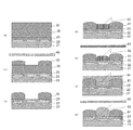
図1は、固体撮像素子の構造を表す端面図である。
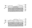
図1(a)(b)に示すように、固体撮像素子は、複数のフォトダイオード22が形成された半導体基板21上に、半導体基板21表面の凹凸を平坦化するための透明平坦化層23、および複数のフォトダイオード22それぞれに対応して形成された複数色のカラーマイクロレンズ61、62、63がこの順に積層されている。複数色のカラーマイクロレンズ61、62、63としては、例えば、緑色の光を透過する緑色カラーマイクロレンズ61、青色の光を透過する青色カラーマイクロレンズ62、赤色の光を透過する赤色カラーマイクロレンズ63がある。カラーマイクロレンズ61、62、63のそれぞれは、フォトダイオード22から遠い側の端部が半球状もしくは放物面状の凸状に形成されている。
Embodiments of the present invention will be described below with reference to the drawings.
(First embodiment)
(Constitution)
FIG. 1 is an end view showing the structure of a solid-state imaging device.
As shown in FIGS. 1A and 1B, the solid-state imaging device has a
また、複数色のカラーマイクロレンズ61、62、63のそれぞれは、色毎(緑、青、赤)に高さが異なっている。具体的には、赤色カラーマイクロレンズ63の高さ>緑色カラーマイクロレンズ61の高さ>青色カラーマイクロレンズ62の高さとなっている。
図2は、カラーフィルタ配列20を表す平面図である。図2に示す配列は、一画素おきにG(緑)フィルタ(緑色カラーマイクロレンズ61)が設けられ、隣り合うGフィルタの間に一行おきにR(赤)フィルタ(赤色カラーマイクロレンズ63)とB(青)フィルタ(青色カラーマイクロレンズ62)とが設けられた、いわゆるベイヤー配列である。
In addition, each of the
FIG. 2 is a plan view showing the
また、カラーマイクロレンズ61、62、63は、透明平坦化層23上に配置されたマイクロレンズ本体部64と、マイクロレンズ本体部64上に形成された直方体状の凸レンズ部65とを備える。凸レンズ部65は、フォトダイオード22の法線方向に凸面を向けた凸レンズ形状に形成されている。これにより、フォトダイオード22から遠い側の端部が半球状もしくは放物面状の凸状、つまり、凸レンズ形状となっている直方体形状を形成している。また、カラーマイクロレンズ61、62、63の高さは、0.2μm以上0.8μm以下とする。さらに、凸レンズ部65の高さは、0.1μm以上0.7μm以下とする。
The
(製造方法)
次に、固体撮像素子の製造方法について説明する。第1実施形態では、カラーマイクロレンズ61、62、63をフォトリソグラフィ方式によって形成する。
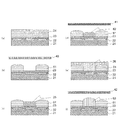
まず、図3(a)に示すように、半導体基板21に複数のフォトダイオード22を形成する。次に、半導体基板21上にシリコン酸化膜またはシリコン窒素酸化膜を形成する。
次に、半導体基板21上に、透明樹脂からなる透明平坦化層(PL)23を形成する。透明平坦化層(PL)23は、半導体基板21表面の凹凸を平坦化するとともに、カラーマイクロレンズ61、62、63と半導体基板21との接着層としての機能を有する。
(Production method)
Next, the manufacturing method of a solid-state image sensor is demonstrated. In the first embodiment, the
First, as shown in FIG. 3A, a plurality of
Next, a transparent planarization layer (PL) 23 made of a transparent resin is formed on the
次に、透明平坦化層23上に、感光性成分を含む緑色カラーレジスト24を塗布する。緑色カラーレジスト24の色材としては、例えば、ピグメントグリーン(PG)36またはPG58とピグメントイエロー(PY)150とを用い、緑色カラーレジスト24の顔料濃度は、例えば50%以上となるように調整することが好ましい。緑色カラーレジスト24の膜厚は、例えば、塗布装置の塗布回転数を1200rpmとすることで500nmとする。また、緑色カラーレジスト24を150度以下(例えば、70度)の温度で加熱することで、完全に硬化はさせないが、ある程度の溶剤耐性を緑色カラーレジスト24に付与する。
Next, a green color resist 24 containing a photosensitive component is applied on the
次に、図3(b)に示すように、半球状または放物面状の凸状に形成可能な透過率分布10を有した緑色領域用のフォトマスク40を用いて、緑色カラーレジスト24にパターン露光および現像を行う。次に、フォトダイオード22の光電変換特性に影響の出ない温度である300度以下(例えば、200度)の温度で熱硬化を行って、緑色カラーマイクロレンズ61を形成する。その際、青色カラーマイクロレンズ62および赤色カラーマイクロレンズ63を形成するための場所から、緑色カラーレジスト24を除去する。
Next, as shown in FIG. 3B, a
図4は、フォトマスク40の1画素辺りの透過率分布10を表す平面図である。
フォトマスク40は、実際に形成するパターンの4倍の寸法を有し、1/4に縮小してパターン露光を行なう。また、フォトマスク40は、同心円で区切られた円形領域、円環状領域毎に濃淡の段階が設定された同心円状の階調(グレースケール)を有する。同心円状の階調は、例えば、1/4縮小時に露光光の波長以下の寸法になる微細な黒ドット(または白ドット)の単位面積当たりの個数をフォトマスク40上で調整して形成する。黒ドットの個数は、中心部に近い領域(円形領域、円環状領域)ほど多くする。これにより、中心部に近い領域(円形領域、円環状領域)ほど透過率が減少する。例えば、中心部の領域(円形領域11)は透過率20〜25%、中心部から2番目の領域(円環状領域12)は透過率25〜30%、3番目の円環状領域13は透過率30〜35%、4番目の円環状領域14は透過率35〜40%、5番目の円環状領域15は透過率40〜45%とする。
FIG. 4 is a plan view showing the
The
なお、青色領域用のフォトマスク41、赤色領域用のフォトマスク42も同様とする。
次に、図3(c)に示すように、透明平坦化層23上に、感光性成分を含む青色カラーレジスト25を塗布する。青色カラーレジスト25の膜厚は、例えば、塗布装置の塗布回転数を2000rpmとすることで400nmとする。また、塗布した青色カラーレジスト25を150度以下(例えば、70度)の温度で加熱することで、完全に硬化はさせないが、ある程度の溶剤耐性を付与する。次に、図3(d)に示すように、半球状または放物面状の凸状に形成可能な透過率分布10を有した青色領域用のフォトマスク41を用いて、青色カラーレジスト25にパターン露光および現像を行う。次に、フォトダイオード22の光電変換特性に影響の出ない温度である300度以下(例えば、200度)の温度で熱硬化を行って、青色カラーマイクロレンズ62を形成する。青色カラーマイクロレンズ62の高さは、緑色カラーマイクロレンズ61よりも低くする。その際、赤色カラーマイクロレンズ63を形成するための場所から、青色カラーレジスト25を除去する。
The same applies to the
Next, as shown in FIG. 3C, a blue color resist 25 containing a photosensitive component is applied on the
次に、図3(e)に示すように、透明平坦化層23上に、感光性成分を含む赤色カラーレジスト26を塗布する。赤色カラーレジスト26の膜厚は、例えば、塗布装置の塗布回転数を800rpmとすることで600nmとする。また、塗布した赤色カラーレジスト26を150度以下(例えば、70度)の温度で加熱することで、完全に硬化はさせないが、ある程度の溶剤耐性を赤色カラーレジスト26に付与する。次に、図3(f)に示すように、半球状または放物面状の凸状に形成可能な透過率分布10を有した赤色領域用のフォトマスク42を用いて、赤色カラーレジスト26にパターン露光および現像を行う。次に、フォトダイオード22の光電変換特性に影響の出ない温度である300度以下(例えば、200度)の温度で熱硬化を行って、赤色カラーマイクロレンズ63を形成する。赤色カラーマイクロレンズ63の高さは、緑色カラーマイクロレンズ61よりも高くする。
Next, as shown in FIG. 3E, a red color resist 26 containing a photosensitive component is applied on the
これにより、色毎に高さの異なるカラーマイクロレンズ61、62、63を作製する。
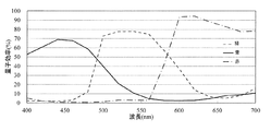
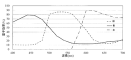
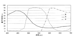
図5は、緑色、青色および赤色といった色の違いに関わらず、高さが全て同じカラーマイクロレンズの各波長に対する各色の量子効率の計測結果を表すグラフである。また、図6は、上述したフォトリソグラフィ方式で形成した、色毎に高さが異なるカラーマイクロレンズ61、62、63の各波長に対する各色の量子効率の計測結果を表すグラフである。図5、図6より、高さが全て同じカラーマイクロレンズの量子効率は各色で差が大きかったが、カラーマイクロレンズの高さを調整することで量子効率の差が小さくなることが確認できた。これにより、第1実施形態の固体撮像素子によれば、3色のカラーマイクロレンズ61、62、63の高さを調整することで、量子効率を制御できることを確認できた。
Thereby, the
FIG. 5 is a graph showing the measurement result of the quantum efficiency of each color for each wavelength of the color microlens having the same height regardless of the difference in color such as green, blue and red. FIG. 6 is a graph showing the measurement results of the quantum efficiencies of the respective colors with respect to the respective wavelengths of the
(第1実施形態の効果)
第1実施形態に係る発明は、以下の効果を奏する。
(1)第1実施形態に係る固体撮像素子は、複数のフォトダイオード22が配置された半導体基板21上に、透明平坦化層23と、複数のフォトダイオード22それぞれに対応して形成された複数色のカラーマイクロレンズ61、62、63とがこの順に積層され、複数色のカラーマイクロレンズ61、62、63のそれぞれの高さが色毎に異なる。
(Effect of 1st Embodiment)
The invention according to the first embodiment has the following effects.
(1) The solid-state imaging device according to the first embodiment includes a plurality of transparent planarization layers 23 and a plurality of
このような構成によれば、カラーマイクロレンズ61、62、63を用いるため、レンズとフォトダイオード22との距離を短くすることができ、量子効率を向上できる。また、カラーマイクロレンズ61、62、63の高さを色毎に調整することで、各色の集光特性の差を低減でき、各色の量子効率の差を低減できる。これにより、量子効率を向上しつつ、各色の量子効率の差を低減可能な固体撮像素子を提供することができる。
According to such a configuration, since the
(2)第1実施形態に係る固体撮像素子は、カラーマイクロレンズ61、62、63は、透明平坦化層23上に配置されたマイクロレンズ本体部64と、マイクロレンズ本体部64上に形成された凸レンズ部65とを備える。そして、カラーマイクロレンズ61、62、63の高さは、0.2μm以上0.8μm以下であり、凸レンズ部65の高さは、0.1μm以上0.7μm以下である。
このような構成によれば、各色の量子効率の差をより適切に低減できる。
(2) In the solid-state imaging device according to the first embodiment, the
According to such a configuration, the difference in quantum efficiency of each color can be reduced more appropriately.
(3)第1実施形態に係る固体撮像素子の製造方法は、カラーマイクロレンズ61、62、63を、感光性成分を含むカラーレジストを用いて、パターン露光、現像および熱硬化を行って形成することを特徴とする。
このような構成によれば、カラーマイクロレンズ61〜63をより容易に形成できる。
(4)第1実施形態に係る固体撮像素子の製造方法は、露光時に、半球状または放物面状の凸状に形成可能な透過率分布10を有したフォトマスク40、41、42を用いる。
このような構成によれば、レンズ形状をより容易に形成できる。
(3) In the method of manufacturing the solid-state imaging device according to the first embodiment, the
According to such a configuration, the
(4) The manufacturing method of the solid-state imaging device according to the first embodiment uses
According to such a configuration, the lens shape can be formed more easily.
(第2実施形態)
次に、本発明の第2実施形態について図面を参照しつつ説明する。なお、第1実施形態と同様な構成等については同一の符号を使用して、その詳細は省略する。
図7は、第2実施形態の固体撮像素子の製造方法を表す端面図である。
図7に示すように、第2実施形態は、固体撮像素子の製造時に、カラーマイクロレンズ61、62、63をエッチング方式で形成する点が第1実施形態と異なる。
(Second Embodiment)
Next, a second embodiment of the present invention will be described with reference to the drawings. In addition, about the structure similar to 1st Embodiment, the same code | symbol is used and the detail is abbreviate | omitted.
FIG. 7 is an end view illustrating the method for manufacturing the solid-state imaging device according to the second embodiment.
As shown in FIG. 7, the second embodiment is different from the first embodiment in that the
(製造方法)
第2実施形態における、固体撮像素子の製造方法について説明する。
まず、図7(a)に示すように、半導体基板21に複数のフォトダイオード22を形成する。次に、半導体基板21上にシリコン酸化膜またはシリコン窒素酸化膜を形成する。次に、半導体基板21上に、透明樹脂からなる透明平坦化層(PL)23を形成する。
(Production method)
The manufacturing method of the solid-state image sensor in 2nd Embodiment is demonstrated.
First, as shown in FIG. 7A, a plurality of
次に、透明平坦化層23上に、感光性成分を含まない緑色顔料分散樹脂液31を塗布する。緑色顔料分散樹脂液31の色材としては、例えば、ピグメントグリーン(PG)36またはPG58と、ピグメントイエロー(PY)150とを用い、緑色顔料分散樹脂液31の顔料濃度が、50%以上となるように調整することが好ましい。緑色顔料分散樹脂液31の膜厚は、例えば、塗布装置の塗布回転数を1000rpmとすることで400nmとする。次に、実デバイスに影響の出ない温度である300度以下(例えば、200度)の温度で加熱することで、熱硬化させ、緑色カラーフィルタ層35を形成する。
Next, a green pigment dispersed resin liquid 31 not containing a photosensitive component is applied on the
次に、緑色カラーフィルタ層35上に、ポジ型レジスト32を塗布する。ポジ型レジスト32の膜厚は、例えば、塗布装置の塗布回転数を1200rpmとすることで1000nmとする。またポジ型レジスト32を90度で加熱する。次に、図7(b)に示すように、半球状または放物面状の凸状に形成可能な透過率分布10を有した緑色領域用のフォトマスク40を用いて、ポジ型レジスト32にパターン露光および現像を行って、半球状または放物面状のレジストパターンを形成する。レジストパターンは、緑色カラーマイクロレンズ61のレンズ母型とする。次に、図7(c)に示すように、半球状または放物面状にパターニングされたポジ型レジスト32をマスクとして緑色カラーフィルタ層35にドライエッチングを行い、シクロヘキサノン等の溶剤によってサンプルを洗浄して、緑色カラーマイクロレンズ61を形成する。その際、青色カラーマイクロレンズ62および赤色カラーマイクロレンズ63を形成するための場所から、緑色顔料分散樹脂液31を除去する。
Next, a positive resist 32 is applied on the green
次に、図7(d)に示すように、透明平坦化層23上に、感光性成分を含む青色カラーレジスト33を塗布する。青色カラーレジスト33の膜厚は、例えば、塗布装置の塗布回転数を1900rpmとすることで400nmとする。また、塗布した青色カラーレジスト33を150度以下(例えば、70度)の温度で加熱することで、完全に硬化はさせないが、ある程度の溶剤耐性を付与する。次に、図7(e)に示すように、半球状または放物面状の凸状に形成可能な透過率分布10を有した青色領域用のフォトマスク41を用いて、青色カラーレジスト33にパターン露光および現像を行う。次に、青色カラーレジスト33に、実デバイスに影響の出ない温度である300度以下(例えば、230度)の温度で熱硬化を行って、青色カラーマイクロレンズ62を形成する。青色カラーマイクロレンズ62の高さは、緑色カラーマイクロレンズ61よりも低くする。その際、赤色カラーマイクロレンズ63を形成するための場所から、青色カラーレジスト33を除去する。
Next, as shown in FIG. 7D, a blue color resist 33 containing a photosensitive component is applied on the
次に、図7(f)に示すように、透明平坦化層23上に、感光性成分を含む赤色カラーレジスト34を塗布する。赤色カラーレジスト34の膜厚は、例えば、塗布装置の塗布回転数を850rpmとすることで600nmとする。また、塗布した赤色カラーレジスト34を150度以下(例えば、70度)の温度で加熱することで、完全に硬化はさせないが、ある程度の溶剤耐性を付与する。次に、図7(g)に示すように、半球状または放物面状の凸状に形成可能な透過率分布10を有した赤色領域用のフォトマスク42を用いて、赤色カラーレジスト34にパターン露光および現像を行う。次に、赤色カラーレジスト34に、実デバイスに影響の出ない温度である300度以下(例えば、230度)の温度で熱硬化を行って、赤色カラーマイクロレンズ63を形成する。赤色カラーマイクロレンズ63の高さは、緑色カラーマイクロレンズ61よりも高くする。
Next, as shown in FIG. 7F, a red color resist 34 containing a photosensitive component is applied on the
これにより、色毎に高さの異なるカラーマイクロレンズ61、62、63を作製する。
なお、その他の構成は第1実施形態と同様である。
このように、第2実施形態では、緑色カラーマイクロレンズ61のみをドライエッチングで形成する例を示したが、同様の手順で、青色カラーマイクロレンズ62、赤色カラーマイクロレンズ63もドライエッチングで形成することもできる。ドライエッチングでパターニングすることにより、顔料分散樹脂液に感光性成分を含まなくてよいため、その分、顔料濃度を増大でき、カラーマイクロレンズ61、62、63の薄膜化が可能となる。
Thereby, the
Other configurations are the same as those in the first embodiment.
As described above, in the second embodiment, an example in which only the
図5は、緑色、青色および赤色といった色の違いに関わらず、高さが全て同じカラーマイクロレンズの各波長に対する各色の量子効率の計測結果を表すグラフである。また、図8は、上述したドライエッチング方式で形成した、色毎に高さが異なるカラーマイクロレンズ61、62、63の各波長に対する各色の量子効率の測定結果を表すグラフである。図5、図8より、高さが全て同じカラーマイクロレンズの量子効率は各色で差が大きかったが、カラーマイクロレンズの高さを調整することで量子効率の差が小さくなることが確認できた。これにより、第2実施形態の固体撮像素子によれば、3色のカラーマイクロレンズ61〜63の高さを調整することで、量子効率を制御できることを確認できた。
FIG. 5 is a graph showing the measurement result of the quantum efficiency of each color for each wavelength of the color microlens having the same height regardless of the difference in color such as green, blue and red. FIG. 8 is a graph showing the measurement results of the quantum efficiencies of the respective colors with respect to the respective wavelengths of the
(第2実施形態の効果)
第2実施形態に係る発明は、第1実施形態の効果に加え、以下の効果を奏する。
(1)第2実施形態に係る固体撮像素子では、複数色のカラーマイクロレンズは、PG36またはPG58とPY150とを有する緑色顔料分散樹脂液31によって形成された緑色カラーマイクロレンズ61を含み、緑色顔料分散樹脂液31の顔料濃度は、50%以上である。
このような構成によれば、感光性成分を含まない緑色顔料分散樹脂液31を用いるため、顔料濃度を増大でき、カラーマイクロレンズ61、62、63を薄膜化できる。
(Effect of 2nd Embodiment)
The invention according to the second embodiment has the following effects in addition to the effects of the first embodiment.
(1) In the solid-state imaging device according to the second embodiment, the color microlenses of a plurality of colors include a
According to such a configuration, since the green pigment dispersion resin liquid 31 containing no photosensitive component is used, the pigment concentration can be increased, and the
(2)第2実施形態に係る固体撮像素子の製造方法は、透明平坦化層23上に感光性成分を含まない顔料分散樹脂液によってカラーフィルタ層(緑色カラーフィルタ層35)を形成し、形成したカラーフィルタ層(緑色カラーフィルタ層35)上にレジストを塗布し、塗布したレジストにパターン露光および現像を行ってレジストパターンを形成し、パターニングされたレジストをマスクとしてカラーフィルタ層(緑色カラーフィルタ層35)にドライエッチングを行うことで、カラーマイクロレンズ61を形成する。
このような構成によれば、カラーマイクロレンズ61〜63をより容易に形成できる。
(3)第2実施形態に係る固体撮像素子の製造方法では、レジストパターンは、カラーマイクロレンズ(緑色カラーマイクロレンズ61)のレンズ母型である。
このような構成によれば、レンズ形状をより容易に形成できる。
(2) In the method of manufacturing the solid-state imaging device according to the second embodiment, the color filter layer (green color filter layer 35) is formed on the
According to such a configuration, the
(3) In the method for manufacturing a solid-state imaging device according to the second embodiment, the resist pattern is a lens matrix of a color microlens (green color microlens 61).
According to such a configuration, the lens shape can be formed more easily.
(第3実施形態)
次に、本発明の第3実施形態について図面を参照しつつ説明する。なお、第1実施形態と同様な構成等については同一の符号を使用して、その詳細は省略する。
図9は、第3実施形態の固体撮像素子の製造方法を表す端面図である。
図9に示すように、第2実施形態は、固体撮像素子の製造時に、互いに隣接するカラーマイクロレンズ61、62、63の境界の半導体基板21側に形成され、屈折率が1.4以上である隔壁53を形成する点が第1実施形態と異なる。
(Third embodiment)
Next, a third embodiment of the present invention will be described with reference to the drawings. In addition, about the structure similar to 1st Embodiment, the same code | symbol is used and the detail is abbreviate | omitted.
FIG. 9 is an end view illustrating the method for manufacturing the solid-state imaging device according to the third embodiment.
As shown in FIG. 9, the second embodiment is formed on the
(製造方法)
次に、第3実施形態における、固体撮像素子の製造方法について説明する。
まず、図9(a)に示すように、半導体基板21に複数のフォトダイオード22を形成する。次に、半導体基板21上にシリコン酸化膜またはシリコン窒素酸化膜を形成する。
次に、半導体基板21上に、物理蒸着(PVD)法によって、合成石英51を膜厚500nmほど蒸着する。合成石英51としては、屈折率が1.4以上のものを採用する。続いて、合成石英51上に、ポジ型レジスト52を塗布する。ポジ型レジスト52の膜厚は、例えば、塗布装置の塗布回転数を800rpmとすることで2000nmとする。次に、図9(b)に示すように、各色のカラーマイクロレンズ61、62、63の境界の半導体基板21側に線幅50nmの格子パターンが転写されるように設計したフォトマスク70を用いて、ポジ型レジスト52を露光および現像し、格子状のレジストパターンを形成する。
(Production method)
Next, the manufacturing method of the solid-state image sensor in 3rd Embodiment is demonstrated.
First, as shown in FIG. 9A, a plurality of
Next,
次に、図9(c)に示すように、格子状にパターニングされたポジ型レジスト52をマスクとして合成石英51にドライエッチングを行い、図9(d)に示すように、シクロヘキサノン等の溶剤によってレジストを洗浄して、合成石英51の隔壁53を形成する。
次に、図9(e)に示すように、形成した隔壁53間の半導体基板21上に、透明樹脂からなる透明平坦化層(PL)23を形成する。次に、透明平坦化層23および隔壁53上に、感光性成分を含む緑色カラーレジスト24を塗布する。緑色カラーレジスト24の色材としては、例えば、ピグメントグリーン(PG)36またはPG58と、ピグメントイエロー(PY)150とを用い、緑色カラーレジスト24の顔料濃度が、50%以上となるように調整することが好ましい。緑色カラーレジスト24の膜厚は、例えば、塗布装置の塗布回転数を1100rpmとすることで550nmとする。また、塗布した緑色カラーレジスト24を150度以下(例えば、70度)の温度で加熱することで、完全に硬化はさせないが、ある程度の溶剤耐性を緑色カラーレジスト24に付与する。
Next, as shown in FIG. 9C, the
Next, as shown in FIG. 9E, a transparent planarization layer (PL) 23 made of a transparent resin is formed on the
次に、図9(f)に示すように、半球状または放物面状の凸状に形成可能な透過率分布10を有した緑色領域用のフォトマスク40を用いて、緑色カラーレジスト24にパターン露光および現像を行う。次に、フォトダイオード22の光電変換特性に影響の出ない温度である300度以下(例えば、200度)の温度で熱硬化を行って、緑色カラーマイクロレンズ61を形成する。その際、青色カラーマイクロレンズ62および赤色カラーマイクロレンズ63を形成するための場所から、緑色カラーレジスト24を除去する。
Next, as shown in FIG. 9F, a
次に、図9(g)に示すように、透明平坦化層23上に、感光性成分を含む青色カラーレジスト25を塗布する。青色カラーレジスト25の膜厚は、例えば、塗布装置の塗布回転数を1900rpmとすることで450nmとする。また、塗布した青色カラーレジスト25を150度以下(例えば、70度)の温度で加熱することで、完全に硬化はさせないが、ある程度の溶剤耐性を付与する。次に、図9(h)に示すように、半球状または放物面状の凸状に形成可能な透過率分布10を有した青色領域用のフォトマスク41を用いて、青色カラーレジスト25にパターン露光および現像を行う。次に、フォトダイオード22の光電変換特性に影響の出ない温度である300度以下(例えば、200度)の温度で熱硬化を行って、青色カラーマイクロレンズ62を形成する。青色カラーマイクロレンズ62の高さは、緑色カラーマイクロレンズ61よりも低くする。その際、赤色カラーマイクロレンズ63を形成するための場所から、青色カラーレジスト25を除去する。
Next, as shown in FIG. 9G, a blue color resist 25 containing a photosensitive component is applied on the
次に、図9(i)に示すように、透明平坦化層23上に、感光性成分を含む赤色カラーレジスト26を塗布する。赤色カラーレジスト26の膜厚は、例えば、塗布装置の塗布回転数を750rpmとすることで650nmとする。また、塗布した赤色カラーレジスト26を150度以下(例えば、70度)の温度で加熱することで、完全に硬化はさせないが、ある程度の溶剤耐性を付与する。次に、図9(j)に示すように、半球状または放物面状の凸状に形成可能な透過率分布10を有した赤色領域用のフォトマスク42を用いて、赤色カラーレジスト26にパターン露光および現像を行う。次に、フォトダイオード22の光電変換特性に影響の出ない温度である300度以下(例えば、200度)の温度で熱硬化を行って、赤色カラーマイクロレンズ63を形成する。赤色カラーマイクロレンズ63の高さは、緑色カラーマイクロレンズ61よりも高くする。
Next, as shown in FIG. 9 (i), a red color resist 26 containing a photosensitive component is applied on the
これにより、色毎に高さの異なるカラーマイクロレンズ61、62、63を作製する。
Thereby, the
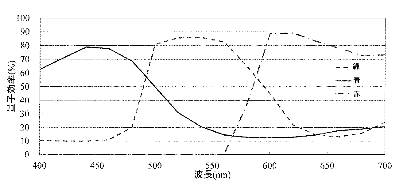
表1は、隔壁53を有する緑色カラーマイクロレンズ61の波長550nmに対する量子効率の計測結果を表すものである。隔壁53は、屈折率が1.1〜1.5の合成石英51を用いて形成した。透明なマイクロレンズと緑色カラーフィルタとを組み合わせからなる従来の構成では、波長550nmに対する量子効率は、77%になった。それゆえ、隔壁53の屈折率は1.4以上が望ましい。これにより、第3実施形態の固体撮像素子は、屈折率1.4以上の隔壁53を有することで、量子効率を向上できることを確認できた。
Table 1 shows the measurement result of the quantum efficiency with respect to the
(第3実施形態の効果)
第3実施形態に係る発明は、第1実施形態の効果に加え、以下の効果を奏する。
(1)本実施形態に係る固体撮像素子は、互いに隣接するカラーマイクロレンズ61、62、63の境界の半導体基板21側に形成され、屈折率が1.4以上である隔壁53を備える。
このような構成によれば、量子効率をより向上することができる。
(Effect of the third embodiment)
The invention according to the third embodiment has the following effects in addition to the effects of the first embodiment.
(1) The solid-state imaging device according to this embodiment includes a
According to such a configuration, the quantum efficiency can be further improved.
10 フォトマスクの透過率分布
11 透過率20〜25%の領域
12 透過率25〜30%の領域
13 透過率30〜35%の領域
14 透過率35〜40%の領域
15 透過率40〜45%の領域
20 カラーフィルタ配列
21 半導体基板
22 フォトダイオード
23 透明平坦化層(PL)
24 緑色カラーレジスト
25 青色カラーレジスト
26 赤色カラーレジスト
31 緑色顔料分散樹脂液
32 ポジ型レジスト
33 青色カラーレジスト
34 赤色カラーレジスト
40 緑色領域用のフォトマスク
41 青色領域用のフォトマスク
42 赤色領域用のフォトマスク
51 合成石英
52 ポジ型レジスト
70 フォトマスク
DESCRIPTION OF
24 Green color resist 25 Blue color resist 26 Red color resist 31 Green pigment
Claims (8)
前記複数色のカラーマイクロレンズのそれぞれの高さが色毎に異なっていることを特徴とする固体撮像素子。 A solid-state imaging device in which a transparent flattening layer and a plurality of color microlenses formed corresponding to each of the plurality of photodiodes are stacked in this order on a semiconductor substrate on which a plurality of photodiodes are arranged. And
A solid-state imaging device, wherein the color microlenses of the plurality of colors have different heights for each color.
前記カラーマイクロレンズの高さは、0.2μm以上0.8μm以下であり、
前記凸レンズ部の高さは、0.1μm以上0.7μm以下であることを特徴とする請求項1に記載の固体撮像素子。 The color microlens includes a microlens main body disposed on the transparent planarization layer, and a convex lens formed on the microlens main body.
The height of the color microlens is 0.2 μm or more and 0.8 μm or less,
2. The solid-state imaging device according to claim 1, wherein a height of the convex lens portion is not less than 0.1 μm and not more than 0.7 μm.
前記緑色顔料分散樹脂液の顔料濃度は、50%以上であることを特徴とする請求項1または2に記載の固体撮像素子。 The multi-color color microlens includes a green color microlens formed of a green pigment dispersion resin liquid having PG36 or PG58 and PY150,
3. The solid-state imaging device according to claim 1, wherein the green pigment-dispersed resin liquid has a pigment concentration of 50% or more.
前記カラーマイクロレンズを、感光性成分を含むカラーレジストを用いて、パターン露光、現像および熱硬化を行って形成することを特徴とする固体撮像素子の製造方法。 It is a manufacturing method of the solid-state image sensing device according to any one of claims 1 to 4,
A method of manufacturing a solid-state imaging device, wherein the color microlens is formed by performing pattern exposure, development, and thermosetting using a color resist containing a photosensitive component.
前記透明平坦化層上に感光性成分を含まない顔料分散樹脂液によってカラーフィルタ層を形成し、形成した前記カラーフィルタ層上にレジストを塗布し、塗布した前記レジストにパターン露光および現像を行ってレジストパターンを形成し、パターニングされた前記レジストをマスクとして前記カラーフィルタ層にドライエッチングを行うことで、前記カラーマイクロレンズを形成することを特徴とする固体撮像素子の製造方法。 It is a manufacturing method of the solid-state image sensing device according to any one of claims 1 to 4,
A color filter layer is formed with a pigment-dispersed resin liquid not containing a photosensitive component on the transparent planarizing layer, a resist is applied on the formed color filter layer, and pattern exposure and development are performed on the applied resist. A method of manufacturing a solid-state imaging device, wherein the color microlens is formed by forming a resist pattern and performing dry etching on the color filter layer using the patterned resist as a mask.
Priority Applications (1)
| Application Number | Priority Date | Filing Date | Title |
|---|---|---|---|
| JP2015255061A JP2017118065A (en) | 2015-12-25 | 2015-12-25 | Solid-state imaging element and method of manufacturing the same |
Applications Claiming Priority (1)
| Application Number | Priority Date | Filing Date | Title |
|---|---|---|---|
| JP2015255061A JP2017118065A (en) | 2015-12-25 | 2015-12-25 | Solid-state imaging element and method of manufacturing the same |
Publications (1)
| Publication Number | Publication Date |
|---|---|
| JP2017118065A true JP2017118065A (en) | 2017-06-29 |
Family
ID=59234610
Family Applications (1)
| Application Number | Title | Priority Date | Filing Date |
|---|---|---|---|
| JP2015255061A Pending JP2017118065A (en) | 2015-12-25 | 2015-12-25 | Solid-state imaging element and method of manufacturing the same |
Country Status (1)
| Country | Link |
|---|---|
| JP (1) | JP2017118065A (en) |
Cited By (1)
| Publication number | Priority date | Publication date | Assignee | Title |
|---|---|---|---|---|
| JP7356184B2 (en) | 2022-02-18 | 2023-10-04 | 有限会社アキュラス | Manufacturing method of light absorber |
-
2015
- 2015-12-25 JP JP2015255061A patent/JP2017118065A/en active Pending
Cited By (1)
| Publication number | Priority date | Publication date | Assignee | Title |
|---|---|---|---|---|
| JP7356184B2 (en) | 2022-02-18 | 2023-10-04 | 有限会社アキュラス | Manufacturing method of light absorber |
Similar Documents
| Publication | Publication Date | Title |
|---|---|---|
| WO2013121742A1 (en) | Image pickup element | |
| JP2006295125A (en) | Solid-state imaging apparatus, its manufacturing method and camera | |
| JP2010272654A (en) | Solid-state image pickup device and manufacturing method thereof | |
| JP2016046510A (en) | Image sensing device and method of manufacturing the same | |
| TW201724479A (en) | Solid-state imaging element and method for manufacturing same | |
| JP2013012518A (en) | Solid state imaging device | |
| TWI467248B (en) | Color filter structure and method for fabricating the same | |
| US20050045805A1 (en) | Solid-state image sensor and a manufacturing method thereof | |
| JP4304987B2 (en) | Solid-state imaging device and manufacturing method thereof | |
| JP2006186203A (en) | Solid-state image pick-up device, manufacturing method therefor, and camera | |
| JP5564751B2 (en) | Manufacturing method of image sensor | |
| JP5027081B2 (en) | Color imaging device and method for manufacturing color imaging device | |
| JP2017118065A (en) | Solid-state imaging element and method of manufacturing the same | |
| WO2013046531A1 (en) | Solid-state image pickup device | |
| JP4175169B2 (en) | Solid-state imaging device and manufacturing method thereof | |
| JP2016219703A (en) | Solid-state imaging element and method for manufacturing solid-state imaging element | |
| JP4497076B2 (en) | Solid-state imaging device and manufacturing method thereof | |
| JP2018110147A (en) | Solid state imaging device and manufacturing method thereof | |
| JP6413700B2 (en) | Solid-state imaging device | |
| JP2009152315A (en) | Image sensor and its manufacturing method | |
| JP4997907B2 (en) | Solid-state imaging device, manufacturing method thereof, and camera | |
| JP2015138918A (en) | Solid state image pickup device, method for manufacturing the same, and camera | |
| JP4547894B2 (en) | Manufacturing method of solid-state imaging device | |
| JP7098912B2 (en) | Solid-state image sensor and its manufacturing method | |
| JP2011165923A (en) | Color solid-state imaging element, and method of manufacturing the same |