JP2017108592A - Switching electric power supply - Google Patents
Switching electric power supply Download PDFInfo
- Publication number
- JP2017108592A JP2017108592A JP2015242584A JP2015242584A JP2017108592A JP 2017108592 A JP2017108592 A JP 2017108592A JP 2015242584 A JP2015242584 A JP 2015242584A JP 2015242584 A JP2015242584 A JP 2015242584A JP 2017108592 A JP2017108592 A JP 2017108592A
- Authority
- JP
- Japan
- Prior art keywords
- switching
- power supply
- voltage
- switching element
- period
- Prior art date
- Legal status (The legal status is an assumption and is not a legal conclusion. Google has not performed a legal analysis and makes no representation as to the accuracy of the status listed.)
- Granted
Links
- 230000001629 suppression Effects 0.000 claims abstract description 28
- 238000004804 winding Methods 0.000 claims description 22
- 230000007704 transition Effects 0.000 claims description 7
- 230000003247 decreasing effect Effects 0.000 claims description 6
- 239000004065 semiconductor Substances 0.000 claims description 5
- 229910002601 GaN Inorganic materials 0.000 claims description 2
- JMASRVWKEDWRBT-UHFFFAOYSA-N Gallium nitride Chemical compound [Ga]#N JMASRVWKEDWRBT-UHFFFAOYSA-N 0.000 claims description 2
- 239000010432 diamond Substances 0.000 claims description 2
- 229910003460 diamond Inorganic materials 0.000 claims description 2
- AJNVQOSZGJRYEI-UHFFFAOYSA-N digallium;oxygen(2-) Chemical compound [O-2].[O-2].[O-2].[Ga+3].[Ga+3] AJNVQOSZGJRYEI-UHFFFAOYSA-N 0.000 claims description 2
- 229910001195 gallium oxide Inorganic materials 0.000 claims description 2
- HBMJWWWQQXIZIP-UHFFFAOYSA-N silicon carbide Chemical compound [Si+]#[C-] HBMJWWWQQXIZIP-UHFFFAOYSA-N 0.000 claims description 2
- 229910010271 silicon carbide Inorganic materials 0.000 claims description 2
- 239000000463 material Substances 0.000 claims 2
- 230000009467 reduction Effects 0.000 abstract description 2
- 239000003990 capacitor Substances 0.000 description 16
- 238000010586 diagram Methods 0.000 description 8
- 238000009499 grossing Methods 0.000 description 3
- 230000004044 response Effects 0.000 description 3
- 238000001514 detection method Methods 0.000 description 2
- XUIMIQQOPSSXEZ-UHFFFAOYSA-N Silicon Chemical compound [Si] XUIMIQQOPSSXEZ-UHFFFAOYSA-N 0.000 description 1
- 230000000295 complement effect Effects 0.000 description 1
- 238000007599 discharging Methods 0.000 description 1
- 238000000034 method Methods 0.000 description 1
- 230000004048 modification Effects 0.000 description 1
- 238000012986 modification Methods 0.000 description 1
- 230000005855 radiation Effects 0.000 description 1
- 230000000630 rising effect Effects 0.000 description 1
- 229910052710 silicon Inorganic materials 0.000 description 1
- 239000010703 silicon Substances 0.000 description 1
- 239000000725 suspension Substances 0.000 description 1
Images


Abstract
Description
本発明は、高効率化のため特に軽負荷状態で適用される間欠動作において、ノイズ低減を図ることのできる簡易な構成のスイッチング電源装置に関する。 The present invention relates to a switching power supply device having a simple configuration capable of reducing noise particularly in intermittent operation applied in a light load state for high efficiency.
スイッチング電源装置は、概略的には直流入力電圧が印加されるトランスの一次巻線に流れる電流を制御する主スイッチング素子と、前記トランスの二次巻線に誘起された電圧を整流・平滑化して所定の直流出力電圧を生成する電圧出力回路を備える。スイッチング電源装置は、更に直流出力電圧に応じたフィードバック信号を入力して前記主スイッチング素子のオン・オフを制御し、これによって直流出力電圧を一定化するスイッチング制御回路を備えて構成される。 The switching power supply generally includes a main switching element that controls a current flowing in a primary winding of a transformer to which a DC input voltage is applied, and a rectifying / smoothing voltage induced in the secondary winding of the transformer. A voltage output circuit for generating a predetermined DC output voltage is provided. The switching power supply device further includes a switching control circuit that inputs a feedback signal corresponding to a DC output voltage to control on / off of the main switching element, thereby making the DC output voltage constant.
ここでスイッチング電源装置の回路方式には、フォワード方式、フライバック方式、電流共振方式、或いは電圧共振方式がある。例として、電流共振型のスイッチング電源装置は図8に示すように構成される。このスイッチング電源装置は、直列に接続された2つのスイッチング素子13,14を主スイッチング素子として備える。スイッチング素子13は、共振用コンデンサ15を介してトランス16の一次巻線に並列接続されており、またスイッチング素子14はトランス16の一次巻線に直列に接続されている。これらのスイッチング素子13,14は、例えばMOS-FETからなり、一般的には集積回路化されたスイッチング制御回路2からのゲート信号を受けて相補的にオン・オフされる。
Here, the circuit system of the switching power supply device includes a forward system, a flyback system, a current resonance system, or a voltage resonance system. As an example, a current resonance type switching power supply device is configured as shown in FIG. This switching power supply device includes two
トランス16の一次巻線には、直流電源から共振用コンデンサ15およびスイッチング素子14を介して直流入力電圧Vinが印加される。前記直流電源は、例えば商用交流電源を整流して直流入力電圧Vinを生成するもので、該直流入力電圧Vinは入力コンデンサ1を介して平滑化されてスイッチング電源装置に与えられる。
A DC input voltage Vin is applied to the primary winding of the
ここでスイッチング素子14は、オン時に共振用コンデンサ15を介してトランス16の一次巻線に電流Icrを流すと共に、共振用コンデンサ15とトランス16の共振インダクタンスとからなる共振回路にエネルギーを蓄積する役割を担う。またスイッチング素子13は、オン時に前記共振回路に蓄えられたエネルギーをトランス16の一次巻線を介して放出させ、該一次巻線に逆向きの電流Icrを流す役割を担う。結果、トランス16の一次巻線を介して流れる電流Icrは、共振の弧を描く正弦波状の波形となる。
Here, when the
このようにしてトランス16の一次巻線に流れる電流Icrにより、該トランスの二次巻線に所定の電圧が誘起される。そしてトランス16の二次巻線にそれぞれ誘起された電圧はダイオード17,18を介して両波整流された後、出力コンデンサ27によって平滑化される。即ち、ダイオード17,18および出力コンデンサ27は、トランス16の二次巻線に誘起された電圧から負荷RLに供給する直流出力電圧Voutを生成する電圧出力回路を構成する。
In this way, a predetermined voltage is induced in the secondary winding of the transformer by the current Icr flowing through the primary winding of the
このように構成されるスイッチング電源装置については、例えば特許文献1等に詳しく紹介される通りである。 The switching power supply configured in this way is as described in detail in, for example, Patent Document 1 and the like.
ところで上述したスイッチング電源装置においては、その定格負荷である100%負荷時には、前記スイッチング素子13,14の相補的なオン・オフに伴ってトランス16の一次巻線に流れる電流Icrがほぼ正弦波となり、効率ηが最大となるように設計される。これに対して軽負荷時には、100%負荷時に比較して電流Icrのピーク値が大きく減少し、トランス16の一次巻線に流れる電流Icrの波形は正弦波の一部を交互に組み合わせた鋸歯状波的なものとなる。このときのトランスの励磁電流自体は、負荷に依らず殆ど変化することはない。この励磁電流は、スイッチング電源装置における、いわゆる無効電流であり、該スイッチング電源装置を構成する回路のインピーダンスに起因する損失の要因となる。これ故、定格負荷において効率ηが最大となるようにスイッチング電源装置を設計しても、軽負荷時の効率ηが低下するという問題がある。
By the way, in the above-described switching power supply device, when the rated load is 100%, the current Icr flowing through the primary winding of the
このような軽負荷時の効率低下を改善する手法として、軽負荷時にはスイッチング素子13,14のオン・オフを所定の停止期間を挟んで間欠的に行わせ、これによってスイッチング損失および導通損失を低減することが行われている。
As a technique for improving the efficiency reduction at such a light load, the
このスイッチング素子13,14の間欠動作は、例えば次のような構成で実現できる。まずスイッチング制御回路2内において、トランス16の二次側に設けられた負荷検出用抵抗Rsを介して取り込んだ電圧信号DETから負荷電力を演算する。スイッチング制御回路2内には、図9に示すように当該負荷電力に応じてスイッチング期間と停止期間の所定のデューティ比を有するスイッチング期間信号VTswを生成する間欠動作制御回路31と駆動回路32を設ける。そして駆動回路32は、間欠動作制御回路31の出力であるスイッチング期間信号VTswなどを入力して、スイッチング期間の間だけスイッチング素子13,14をオン・オフするゲート信号HO,LOを生成する。
The intermittent operation of the
この結果、前記スイッチング素子13,14のオン・オフ動作の停止期間における該スイッチング素子13,14のスイッチング損失等がなくなり、これによって軽負荷時における全体的な効率ηの低下が防止される。間欠動作制御回路については、例えば特許文献2〜5に詳しく紹介されている。
As a result, there is no switching loss or the like of the
しかしながら、上述した特許文献に代表される従来の間欠動作は、例えば図10において、ローサイドスイッチング素子14のドレイン電流IDLの波形に見られるように、スイッチング素子のドレイン−ソース間電圧VSが高いタイミングで、停止期間からスイッチング期間に移行するためハードスイッチングとなる。このため、このタイミングでサージ電流が発生しEMIノイズを発生させるという問題があった。
However, the conventional intermittent operation typified by the above-described patent document, for example, at the timing when the drain-source voltage VS of the switching element is high as seen in the waveform of the drain current IDL of the low-
一方で、CISPR等に代表されるEMC規格の要求から、スイッチング電源の低ノイズ化が求められている。低ノイズ化の実現のためには、チョークコイルやコンデンサ等の受動部品を用いることが考えられるが、装置の大型化や部品点数の増加を招き、また高コスト化の要因にもなるという問題がある。 On the other hand, the noise of switching power supplies is required to meet the requirements of EMC standards represented by CISPR and the like. To realize low noise, it is conceivable to use passive components such as choke coils and capacitors. However, there is a problem that the size of the device is increased, the number of components is increased, and the cost is increased. is there.
本発明はかかる従来の事情に対処してなされたものであり、間欠動作で生じるEMIノイズの低減を安価に実現することのできるスイッチング電源装置を提供することを目的とする。 The present invention has been made in response to such a conventional situation, and an object of the present invention is to provide a switching power supply apparatus that can reduce EMI noise caused by intermittent operation at low cost.
上記目的を達成するため、本発明のスイッチング電源装置は、間欠動作時において、スイッチング期間から停止期間に移行したタイミングで主スイッチング素子のゲート抵抗値(駆動抵抗値)をスイッチング動作時の通常のゲート抵抗値よりも大きくしておき、スイッチング期間移行後の最初のスイッチング動作の途中で前記通常の抵抗値に戻して、ゲート電流(駆動電流)を増加させる回路を備える。これにより、スイッチング期間開始後の最初のスイッチング動作ではゲート電圧が緩やかに上昇するため、ドレイン電流、または、コレクタ電流のサージを抑制することができる。なお、ゲート抵抗の切換は、ドレイン電圧、または、コレクタ電圧を検出し、その値が充分に低くなったときにゲート抵抗値を低減し、主スイッチング素子をフルオンすることでソフトスイッチングを実現する。
具体的には、本発明に係るスイッチング電源装置は、直流入力電圧が印加されるトランスの一次巻線に流れる電流を制御する主スイッチング素子、並びに前記トランスの二次巻線に誘起された電圧を整流して所定の直流出力電圧を生成する電圧出力回路を備えたスイッチング電源本体と、
前記直流出力電圧に応じたフィードバック信号を入力して前記主スイッチング素子をオン・オフするスイッチング信号の周波数を制御して前記直流出力電圧を一定化するスイッチング制御回路とを具備するスイッチング電源装置であって、
前記主スイッチング素子のドレイン−ソース間電圧信号またはコレクタ−エミッタ間電圧信号を取りこみ、取り込んだ前記電圧信号の電圧値と予め設定した閾値とを比較するコンパレータの出力、および、前記スイッチング信号でスイッチングを行うスイッチング期間とスイッチングを行わない停止期間とを切り換えるスイッチング期間信号を用いて、前記主スイッチング素子の駆動電流値または駆動抵抗値を切り換えるサージ電流抑制回路を備え、
当該サージ電流抑制回路は、前記停止期間から前記スイッチング期間に移行後、前記電圧信号の電圧値が前記閾値以下に低下したことを検出して、前記主スイッチング素子の駆動電流値を増加、または、駆動抵抗値を減少させ、その後、前記スイッチング期間から前記停止期間に移行したことを検出し、前記主スイッチング素子の駆動電流値を減少、または、駆動抵抗値を増加させることを特徴とする。
In order to achieve the above object, the switching power supply device of the present invention is configured such that the gate resistance value (drive resistance value) of the main switching element is changed to the normal gate during the switching operation at the timing when the switching period is shifted to the stop period during the intermittent operation. A circuit that increases the gate current (driving current) by setting the resistance value higher than the resistance value and returning to the normal resistance value during the first switching operation after the transition to the switching period is provided. Thereby, in the first switching operation after the start of the switching period, the gate voltage gradually rises, so that the surge of the drain current or the collector current can be suppressed. The switching of the gate resistance is realized by detecting the drain voltage or the collector voltage, reducing the gate resistance value when the value becomes sufficiently low, and realizing the soft switching by fully turning on the main switching element.
Specifically, the switching power supply according to the present invention includes a main switching element that controls a current flowing in a primary winding of a transformer to which a DC input voltage is applied, and a voltage induced in the secondary winding of the transformer. A switching power supply body including a voltage output circuit that rectifies and generates a predetermined DC output voltage;
A switching power supply device comprising: a switching control circuit that inputs a feedback signal corresponding to the DC output voltage and controls the frequency of a switching signal for turning on and off the main switching element to make the DC output voltage constant. And
The drain-source voltage signal or the collector-emitter voltage signal of the main switching element is taken in, the output of the comparator that compares the voltage value of the fetched voltage signal with a preset threshold value, and switching is performed by the switching signal. Using a switching period signal that switches between a switching period to perform and a stop period in which switching is not performed, and a surge current suppression circuit that switches a driving current value or a driving resistance value of the main switching element,
The surge current suppression circuit detects that the voltage value of the voltage signal has dropped below the threshold after the transition from the stop period to the switching period, or increases the drive current value of the main switching element, or The drive resistance value is decreased, and then the transition from the switching period to the stop period is detected, and the drive current value of the main switching element is decreased or the drive resistance value is increased.
前記主スイッチング素子や、前記トランスの二次巻線の誘起電圧を整流する素子の一部は、ワイドバンドギャップ半導体で形成することもできる。 The main switching element and a part of the element that rectifies the induced voltage of the secondary winding of the transformer may be formed of a wide band gap semiconductor.
以上、本発明のスイッチング電源装置は、間欠動作における停止期間からスイッチング期間に移行後、主スイッチング素子のドレイン−ソース間電圧またはコレクタ−エミッタ間電圧が閾値以下に低下したことを検出して、主スイッチング素子の駆動電流値を増加させ、または駆動抵抗値を減少させている。このため本発明のスイッチング電源装置は、スイッチング期間の開始時に生じる急峻なサージ電流を抑制することができ、このサージ電流に起因する伝導ノイズや放射ノイズの低減を図ることができる。 As described above, the switching power supply device according to the present invention detects that the drain-source voltage or the collector-emitter voltage of the main switching element has dropped below the threshold value after the transition from the stop period in the intermittent operation to the switching period. The drive current value of the switching element is increased or the drive resistance value is decreased. Therefore, the switching power supply device of the present invention can suppress a steep surge current generated at the start of the switching period, and can reduce conduction noise and radiation noise caused by the surge current.
以下、本発明の実施の形態について図面を参照しながら説明する。なお本実施の形態では、ハーフブリッジ電流共振回路を例にとって説明するが、例えばフライバック、フォワード、フルブリッジ電流共振回路、電圧共振回路等の他の方式のスイッチング電源装置についても同様に適用できる。 Hereinafter, embodiments of the present invention will be described with reference to the drawings. In this embodiment, a half-bridge current resonance circuit will be described as an example. However, the present invention can be similarly applied to other types of switching power supply devices such as flyback, forward, full-bridge current resonance circuit, and voltage resonance circuit.
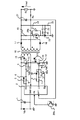
図1は本発明の第1の実施の形態によるスイッチング電源装置の構成を示す回路図である。図8に示す従来の回路との違いは、抵抗器8とスイッチ7とを並列接続したサージ電流抑制回路40aを、スイッチング制御回路2のローサイドゲート信号出力端子LOからローサイドスイッチング素子14のゲートへ至る信号路に介挿したことである。また、スイッチング制御回路2には、図2に示すようにサージ電流抑制回路(制御側)40bを追加した。サージ電流抑制回路(制御側)40bの出力信号Rgによってスイッチ7の導通・開放状態を切り換える。このスイッチ7を有しスイッチング素子14の駆動電流を切り換えるサージ電流抑制回路40aと、スイッチ7への切換信号(Rg)を生成するサージ電流抑制回路(制御側)40bとでサージ電流抑制回路40を構成する。その他は図8、図9と同様であるので、同一要素には同一符号を付して説明を省略する。なお、本実施の形態では、サージ電流抑制回路(制御側)40bをスイッチング制御回路2に内蔵する構成としているが、スイッチング制御回路2の外部に設けるようにしても良い。
FIG. 1 is a circuit diagram showing a configuration of a switching power supply device according to a first embodiment of the present invention. The difference from the conventional circuit shown in FIG. 8 is that a surge current suppressing
また、本実施の形態では、間欠動作時に必ずローサイドスイッチング素子14からターンオンさせることを前提としているため、サージ電流抑制回路40aはローサイド側のみに適用している。したがって、例えばハイサイドスイッチング素子13から必ずターンオンさせるように回路構成する場合は、ハイサイド側のみにサージ電流抑制回路40aを介挿すれば良い。一方、ターンオン開始がハイサイド/ローサイドのどちらかに規定されていないような場合、即ちスイッチング期間への移行時にハイサイド/ローサイドのいずれのスイッチング素子から動作を開始するのか不定の場合には、ハイサイド/ローサイド共にサージ電流抑制回路40aを介挿する必要がある。
In the present embodiment, since it is assumed that the low-
スイッチング制御回路2の内蔵するサージ電流抑制回路(制御側)40bは、図3に示すように、ローサイドのドレイン−ソース間電圧VSと予め設定された閾値電圧VSthとを比較し、比較結果を出力するコンパレータ60と、間欠動作制御回路31からの出力信号VTswと前記コンパレータ60からの出力信号を入力して、サージ電流抑制回路40aへの切換信号Rgを出力する駆動電流値/抵抗値切換回路50から構成されている。
As shown in FIG. 3, the surge current suppression circuit (control side) 40b built in the switching
サージ電流抑制回路(制御側)40bの論理回路図の一例を図4に示す。この図において、コンパレータ60は、ローサイドのドレイン−ソース間電圧VSが閾値電圧VSthを下回ったときに論理「1」を出力する。コンパレータ60の出力と、スイッチング期間信号VTswは、論理積を演算する第1のAND回路55の入力端子に夫々接続されている。また、スイッチング期間信号VTswの立ち下がりで時間Tの間のみ論理「1」となるパルスを出力する単安定マルチ回路51を備える。この単安定マルチ回路51の出力端子Qは、第2のAND回路54の入力端子に接続され、また当該出力端子Qは抵抗器52を介して第2のAND回路54の他の入力端子に接続されている。また第2のAND回路54の抵抗器52側の入力端子は、コンデンサ53を介して基準電位に接続されている。この抵抗器52とコンデンサ53は、時定数τのRCフィルタを構成する。なお、前記単安定マルチ回路51の1ショットパルス幅Tは、時定数τで設定される遅延時間よりも若干大きく設定される。
An example of a logic circuit diagram of the surge current suppression circuit (control side) 40b is shown in FIG. In this figure, the
第1のAND回路55の出力端子はRSフリップフロップ56のセット入力端子Sに接続され、第2のAND回路54の出力端子は、RSフリップフロップ56のリセット入力端子Rに夫々接続されている。RSフリップフロップ56の否定出力Q*(ここで「*」は否定を表す。)は、スイッチ7を制御する切換信号Rgとして出力される。
The output terminal of the first AND
サージ電流抑制回路40aは、切換信号Rgが論理「1」の時に、スイッチ7が開放状態となり、スイッチング制御回路2のLO出力は、抵抗器8、抵抗器11を介してローサイドスイッチング素子14のゲート端子に供給される。切換信号Rgが論理「0」の時には、スイッチ7は導通状態となり、スイッチング制御回路2のLO出力は抵抗器8を介さずにローサイドスイッチング素子14のゲート端子に供給される。
In the surge
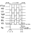
図5は間欠動作時の主回路、及び各部の動作を示したタイミングチャートである。VTswはスイッチング期間信号、HO、LOは間欠動作時のハイサイド/ローサイドスイッチング素子13,14の駆動信号、VgH、VgLはハイサイド/ローサイドスイッチング素子13,14のゲート電圧信号、IDLはローサイドスイッチング素子14のドレイン電流、VSはローサイドスイッチング素子14のドレイン−ソース間電圧信号、Rgはサージ電流抑制回路(制御側)40bから出力されるスイッチ切換信号である。
FIG. 5 is a timing chart showing the operation of the main circuit and each part during intermittent operation. VTsw is a switching period signal, HO and LO are driving signals for the high-side / low-
以下、図5のタイミングチャートを参照しながら、本実施の形態によるスイッチング電源装置の動作を説明する。図5において、t1は間欠動作時のスイッチング期間の再開タイミングである。同タイミングでローサイドスイッチング素子14のゲート抵抗は抵抗器8と抵抗器11の直列抵抗となる。このため、例えば抵抗器8の抵抗値を抵抗器11の抵抗値に対し10倍程度とすれば、ローサイドスイッチング素子14のスイッチング応答をほぼ10倍鈍化させることができる。したがって、VgLの立ち上がり速度は抵抗器8を介さない場合に比べて鈍くなる。
Hereinafter, the operation of the switching power supply according to the present embodiment will be described with reference to the timing chart of FIG. In FIG. 5, t1 is the restart timing of the switching period during intermittent operation. At the same timing, the gate resistance of the low-
その後、t2のタイミングでVgLがミラー領域に達して徐々にIDLが流れ始める。その結果、VSが徐々に下がり続け、予め設定した閾値電圧VSthと交差する。このタイミングt3で、コンパレータ60の出力は論理「1」になる。このとき、スイッチング期間信号VTswも論理「1」(スイッチング期間)である。よって、第1のAND回路55の出力は論理「1」になる。したがって、RSフリップフロップ56のセット入力が論理「1」になり、RSフリップフロップ56の否定出力である切換信号Rgは論理「0」になる。これにより、スイッチ7は導通状態になり、ローサイドスイッチング素子14のゲート抵抗値は抵抗器11の抵抗値(抵抗器8の抵抗値のほぼ1/10)となり、その結果VgLが急峻に立ち上がる。このとき、VS=VSthであるため、実用的にはVSthを数V〜数十Vに設定すればハードスイッチングを避けることができる。
Thereafter, VgL reaches the mirror region at the timing of t2, and IDL begins to flow gradually. As a result, VS continues to decrease gradually and crosses a preset threshold voltage VSth. At this timing t3, the output of the
その後、サージ電流抑制回路(制御側)40bは、タイミングt4においてスイッチング期間信号VTswが論理「0」、即ちスイッチング期間が終了したことを検出すると、上記単安定マルチ回路51はパルス幅Tの1ショットパルスを出力する。すると、第2のAND回路54は時定数τで設定された遅延時間後にRSフリップフロップ56にリセットパルスを出力する。これにより、切換信号Rgは時定数τで設定された遅延時間後(タイミングt5)に論理「1」となり、スイッチ7は開放状態になる。すると、ゲート抵抗値は小さい値(抵抗器11のみの抵抗値)から大きい値(抵抗器8と抵抗器11の合計抵抗値)に切り換わる。なお前記遅延時間は、スイッチング素子が確実にターンオフしてから切換信号Rgが立ち上がるように設定される。
Thereafter, when the surge current suppression circuit (control side) 40b detects that the switching period signal VTsw is logic “0” at timing t4, that is, the switching period has ended, the monostable multi-circuit 51 performs one shot of the pulse width T. Output a pulse. Then, the second AND
以上、本実施の形態によるスイッチング電源装置によれば、従来回路では間欠動作におけるスイッチング期間の開始タイミングt1において発生していたサージ電流(図10参照)を抑制した間欠動作が可能となり、低ノイズと効率改善の両立を図ることができる。 As described above, according to the switching power supply according to the present embodiment, the conventional circuit can perform the intermittent operation while suppressing the surge current (see FIG. 10) generated at the start timing t1 of the switching period in the intermittent operation. Both efficiency improvements can be achieved.
次に本発明の第2の実施の形態について説明する。
本実施の形態によるスイッチ電源装置は、サージ電流抑制回路40aを、従来のゲート抵抗と一体として構成したものである。即ち本実施の形態によるサージ電流抑制回路40aは、図6に示すように、抵抗器11と直列に、かつ抵抗器9とダイオード10の直列回路と並列になるように挿入されている。この回路構成により、LO出力が論理「1」になったときには駆動電流が抑制され、LO出力が論理「0」になったときには、並列に接続された抵抗器9によってゲート電流の引き込み能力を十分に確保することが可能になる。このため、第2の実施形態は、第1の実施の形態における時定数τによる切換信号Rgの戻り時間の調整を行う必要がない。すなわち、本実施の形態のサージ電流抑制回路40aを適用することにより、図7に示すように駆動電流値/抵抗値切換回路50のRC回路を省くことができる。これにより、より簡易な構成でスイッチング制御回路を実現することができる。
Next, a second embodiment of the present invention will be described.
The switch power supply according to the present embodiment is configured such that the surge
本発明は、上述の実施の形態に限定されることなく、その要旨を逸脱しない範囲で種々変形して実施することができる。例えば、高速スイッチングによりスイッチング損失を低減し、効率を改善するため、従来多用されているシリコンの半導体の代わりに、主スイッチング素子、または二次巻線の誘起電圧を整流する素子の一部、若しくはその全てを炭化珪素、窒化ガリウム、酸化ガリウム、ダイヤモンド等のワイドバンドギャップ半導体で構成した素子とすることも勿論可能である。 The present invention is not limited to the above-described embodiments, and can be implemented with various modifications without departing from the scope of the invention. For example, in order to reduce switching loss and improve efficiency by high-speed switching, instead of a silicon semiconductor that has been widely used in the past, a part of the main switching element or an element that rectifies the induced voltage of the secondary winding, or Of course, it is possible to make all of these elements composed of wide band gap semiconductors such as silicon carbide, gallium nitride, gallium oxide, and diamond.
1 平滑コンデンサ(入力コンデンサ)
2 スイッチング制御回路
3 ハイサイドスイッチング素子ターンオフ抵抗
4 ハイサイドスイッチング素子ターンオフダイオード
5 ハイサイドスイッチング素子ターンオン抵抗
6 ハイサイドスイッチング素子ゲート−ソース間抵抗
7 スイッチ(サージ電流抑制回路40の一部)
8 抵抗(サージ電流抑制回路40の一部)
9 ローサイドスイッチング素子ターンオフ抵抗
10 ローサイドスイッチング素子ターンオフダイオード
11 ローサイドスイッチング素子ターンオン抵抗
12 ハイサイドスイッチング素子ゲート−ソース間抵抗
13 ハイサイドスイッチング素子
14 ローサイドスイッチング素子
15 共振コンデンサ
16 トランス
17,18 整流ダイオード
19,21,22,24,26,52 抵抗器
20a、20b フォトカプラ
23 シャントレギュレータ
25,53 コンデンサ
27 2次側平滑コンデンサ(出力コンデンサ)
31 間欠動作制御回路
32 駆動回路
40 サージ電流抑制回路
50 駆動電流値/抵抗値切換回路
51 単安定マルチ回路(単安定マルチバイブレータ)
56 RSフリップフロップ
54,55 AND回路
60 コンパレータ
Rs 負荷検出用抵抗
RL 負荷
1 Smoothing capacitor (input capacitor)
2 switching
8 Resistance (part of surge current suppression circuit 40)
9 Low-side switching element turn-off
31 intermittent
56 RS flip-
Claims (5)
前記直流出力電圧に応じたフィードバック信号を入力して前記主スイッチング素子をオン・オフするスイッチング信号の周波数を制御して前記直流出力電圧を一定化するスイッチング制御回路とを具備するスイッチング電源装置であって、
前記主スイッチング素子のドレイン−ソース間電圧信号またはコレクタ−エミッタ間電圧信号を取りこみ、取り込んだ前記電圧信号の電圧値と予め設定した閾値とを比較するコンパレータの出力、および、前記スイッチング信号でスイッチングを行うスイッチング期間とスイッチングを行わない停止期間とを切り換えるスイッチング期間信号を用いて、前記主スイッチング素子の駆動電流値または駆動抵抗値を切り換えるサージ電流抑制回路を備え、
当該サージ電流抑制回路は、前記停止期間から前記スイッチング期間に移行後、前記電圧信号の電圧値が前記閾値以下に低下したことを検出して、前記主スイッチング素子の駆動電流値を増加、または、駆動抵抗値を減少させ、その後、前記スイッチング期間から前記停止期間に移行したことを検出し、前記主スイッチング素子の駆動電流値を減少、または、駆動抵抗値を増加させることを特徴とするスイッチング電源装置。 A main switching element that controls a current flowing in a primary winding of a transformer to which a DC input voltage is applied, and a voltage output circuit that rectifies a voltage induced in the secondary winding of the transformer and generates a predetermined DC output voltage A switching power supply body with
A switching power supply device comprising: a switching control circuit that inputs a feedback signal corresponding to the DC output voltage and controls the frequency of a switching signal for turning on and off the main switching element to make the DC output voltage constant. And
The drain-source voltage signal or the collector-emitter voltage signal of the main switching element is taken in, the output of the comparator that compares the voltage value of the fetched voltage signal with a preset threshold value, and switching is performed by the switching signal. Using a switching period signal that switches between a switching period to perform and a stop period in which switching is not performed, and a surge current suppression circuit that switches a driving current value or a driving resistance value of the main switching element,
The surge current suppression circuit detects that the voltage value of the voltage signal has dropped below the threshold after the transition from the stop period to the switching period, or increases the drive current value of the main switching element, or A switching power supply characterized in that the drive resistance value is decreased, and then the transition from the switching period to the stop period is detected, and the drive current value of the main switching element is decreased or the drive resistance value is increased. apparatus.
Priority Applications (1)
| Application Number | Priority Date | Filing Date | Title |
|---|---|---|---|
| JP2015242584A JP6607018B2 (en) | 2015-12-11 | 2015-12-11 | Switching power supply |
Applications Claiming Priority (1)
| Application Number | Priority Date | Filing Date | Title |
|---|---|---|---|
| JP2015242584A JP6607018B2 (en) | 2015-12-11 | 2015-12-11 | Switching power supply |
Publications (2)
| Publication Number | Publication Date |
|---|---|
| JP2017108592A true JP2017108592A (en) | 2017-06-15 |
| JP6607018B2 JP6607018B2 (en) | 2019-11-20 |
Family
ID=59061097
Family Applications (1)
| Application Number | Title | Priority Date | Filing Date |
|---|---|---|---|
| JP2015242584A Active JP6607018B2 (en) | 2015-12-11 | 2015-12-11 | Switching power supply |
Country Status (1)
| Country | Link |
|---|---|
| JP (1) | JP6607018B2 (en) |
Cited By (2)
| Publication number | Priority date | Publication date | Assignee | Title |
|---|---|---|---|---|
| CN109449878A (en) * | 2018-10-24 | 2019-03-08 | 湖南大学 | Low-voltage direct intelligent switch control system |
| JP2020058213A (en) * | 2018-10-02 | 2020-04-09 | 富士電機株式会社 | Control device of switching power supply device |
Citations (5)
| Publication number | Priority date | Publication date | Assignee | Title |
|---|---|---|---|---|
| JP2002315333A (en) * | 2001-04-10 | 2002-10-25 | Shindengen Electric Mfg Co Ltd | Switching power supply device |
| JP2008109766A (en) * | 2006-10-25 | 2008-05-08 | Sanken Electric Co Ltd | Power conversion device and control method therefor |
| JP2015077007A (en) * | 2013-10-09 | 2015-04-20 | コーセル株式会社 | Switching power supply device |
| US20150263629A1 (en) * | 2014-03-17 | 2015-09-17 | Semiconductor Components Industries, Llc | Method and apparatus for dedicated skip mode for resonant converters |
| WO2015138880A1 (en) * | 2014-03-14 | 2015-09-17 | Avogy, Inc. | Adaptive synchronous switching in a resonant converter |
-
2015
- 2015-12-11 JP JP2015242584A patent/JP6607018B2/en active Active
Patent Citations (5)
| Publication number | Priority date | Publication date | Assignee | Title |
|---|---|---|---|---|
| JP2002315333A (en) * | 2001-04-10 | 2002-10-25 | Shindengen Electric Mfg Co Ltd | Switching power supply device |
| JP2008109766A (en) * | 2006-10-25 | 2008-05-08 | Sanken Electric Co Ltd | Power conversion device and control method therefor |
| JP2015077007A (en) * | 2013-10-09 | 2015-04-20 | コーセル株式会社 | Switching power supply device |
| WO2015138880A1 (en) * | 2014-03-14 | 2015-09-17 | Avogy, Inc. | Adaptive synchronous switching in a resonant converter |
| US20150263629A1 (en) * | 2014-03-17 | 2015-09-17 | Semiconductor Components Industries, Llc | Method and apparatus for dedicated skip mode for resonant converters |
Cited By (3)
| Publication number | Priority date | Publication date | Assignee | Title |
|---|---|---|---|---|
| JP2020058213A (en) * | 2018-10-02 | 2020-04-09 | 富士電機株式会社 | Control device of switching power supply device |
| JP7400188B2 (en) | 2018-10-02 | 2023-12-19 | 富士電機株式会社 | Control device |
| CN109449878A (en) * | 2018-10-24 | 2019-03-08 | 湖南大学 | Low-voltage direct intelligent switch control system |
Also Published As
| Publication number | Publication date |
|---|---|
| JP6607018B2 (en) | 2019-11-20 |
Similar Documents
| Publication | Publication Date | Title |
|---|---|---|
| JP6287473B2 (en) | Bridgeless power factor correction converter | |
| CN106059304B (en) | Switch with efficient voltage reduction using secondary switches | |
| US9614448B2 (en) | Switching power-supply device | |
| US8335097B2 (en) | Semiconductor device that converts input direct current voltage to regulated output voltage by intermittently switching on and off the input direct current voltage | |
| US6366476B1 (en) | Switching power supply apparatus with active clamp circuit | |
| US9906147B2 (en) | Adaptive dead time control apparatus and method for switching power converters | |
| JP4701749B2 (en) | DC converter | |
| JP4626338B2 (en) | DC converter | |
| TWI542131B (en) | Switchable buck converter with?zero voltage switching capability operating with a stabilized switching frequency | |
| US10581318B2 (en) | Resonant converter including capacitance addition circuits | |
| JP2008109775A (en) | Dc-dc converter and control method therefor | |
| US9887634B2 (en) | Circuits and methods for synchronous rectification in resonant converters | |
| WO1995034120A1 (en) | Pulse width modulated dc-to-dc boost converter | |
| JP2008289336A (en) | Switching power supply apparatus | |
| JP5549659B2 (en) | Switching power supply | |
| JP6698157B2 (en) | Resonant system controller and predictive soft switching per cycle | |
| JP6607018B2 (en) | Switching power supply | |
| JP5516055B2 (en) | Power converter | |
| JP6783738B2 (en) | converter | |
| WO2015178106A1 (en) | Power supply device | |
| JP2015228760A (en) | Switching power supply | |
| CN113812076A (en) | Mode operation detection for controlling power converter with active clamp switch | |
| US20190207530A1 (en) | Power supply circuit | |
| JP6366558B2 (en) | Switching power supply | |
| JP2011041387A (en) | Dc-dc conversion circuit |
Legal Events
| Date | Code | Title | Description |
|---|---|---|---|
| A621 | Written request for application examination |
Free format text: JAPANESE INTERMEDIATE CODE: A621 Effective date: 20181114 |
|
| A977 | Report on retrieval |
Free format text: JAPANESE INTERMEDIATE CODE: A971007 Effective date: 20190904 |
|
| TRDD | Decision of grant or rejection written | ||
| A01 | Written decision to grant a patent or to grant a registration (utility model) |
Free format text: JAPANESE INTERMEDIATE CODE: A01 Effective date: 20190924 |
|
| A61 | First payment of annual fees (during grant procedure) |
Free format text: JAPANESE INTERMEDIATE CODE: A61 Effective date: 20191007 |
|
| R150 | Certificate of patent or registration of utility model |
Ref document number: 6607018 Country of ref document: JP Free format text: JAPANESE INTERMEDIATE CODE: R150 |
|
| R250 | Receipt of annual fees |
Free format text: JAPANESE INTERMEDIATE CODE: R250 |
|
| R250 | Receipt of annual fees |
Free format text: JAPANESE INTERMEDIATE CODE: R250 |